WO2014174804A1 - El表示装置の製造方法 - Google Patents
El表示装置の製造方法 Download PDFInfo
- Publication number
- WO2014174804A1 WO2014174804A1 PCT/JP2014/002158 JP2014002158W WO2014174804A1 WO 2014174804 A1 WO2014174804 A1 WO 2014174804A1 JP 2014002158 W JP2014002158 W JP 2014002158W WO 2014174804 A1 WO2014174804 A1 WO 2014174804A1
- Authority
- WO
- WIPO (PCT)
- Prior art keywords
- light emitting
- display device
- substrate
- thin film
- mask
- Prior art date
- Legal status (The legal status is an assumption and is not a legal conclusion. Google has not performed a legal analysis and makes no representation as to the accuracy of the status listed.)
- Ceased
Links
Images


Classifications
-
- C—CHEMISTRY; METALLURGY
- C23—COATING METALLIC MATERIAL; COATING MATERIAL WITH METALLIC MATERIAL; CHEMICAL SURFACE TREATMENT; DIFFUSION TREATMENT OF METALLIC MATERIAL; COATING BY VACUUM EVAPORATION, BY SPUTTERING, BY ION IMPLANTATION OR BY CHEMICAL VAPOUR DEPOSITION, IN GENERAL; INHIBITING CORROSION OF METALLIC MATERIAL OR INCRUSTATION IN GENERAL
- C23C—COATING METALLIC MATERIAL; COATING MATERIAL WITH METALLIC MATERIAL; SURFACE TREATMENT OF METALLIC MATERIAL BY DIFFUSION INTO THE SURFACE, BY CHEMICAL CONVERSION OR SUBSTITUTION; COATING BY VACUUM EVAPORATION, BY SPUTTERING, BY ION IMPLANTATION OR BY CHEMICAL VAPOUR DEPOSITION, IN GENERAL
- C23C16/00—Chemical coating by decomposition of gaseous compounds, without leaving reaction products of surface material in the coating, i.e. chemical vapour deposition [CVD] processes
- C23C16/04—Coating on selected surface areas, e.g. using masks
- C23C16/042—Coating on selected surface areas, e.g. using masks using masks
-
- H—ELECTRICITY
- H10—SEMICONDUCTOR DEVICES; ELECTRIC SOLID-STATE DEVICES NOT OTHERWISE PROVIDED FOR
- H10K—ORGANIC ELECTRIC SOLID-STATE DEVICES
- H10K50/00—Organic light-emitting devices
- H10K50/80—Constructional details
- H10K50/84—Passivation; Containers; Encapsulations
- H10K50/841—Self-supporting sealing arrangements
-
- H—ELECTRICITY
- H10—SEMICONDUCTOR DEVICES; ELECTRIC SOLID-STATE DEVICES NOT OTHERWISE PROVIDED FOR
- H10K—ORGANIC ELECTRIC SOLID-STATE DEVICES
- H10K50/00—Organic light-emitting devices
- H10K50/80—Constructional details
- H10K50/84—Passivation; Containers; Encapsulations
- H10K50/842—Containers
- H10K50/8426—Peripheral sealing arrangements, e.g. adhesives, sealants
-
- H—ELECTRICITY
- H10—SEMICONDUCTOR DEVICES; ELECTRIC SOLID-STATE DEVICES NOT OTHERWISE PROVIDED FOR
- H10K—ORGANIC ELECTRIC SOLID-STATE DEVICES
- H10K50/00—Organic light-emitting devices
- H10K50/80—Constructional details
- H10K50/84—Passivation; Containers; Encapsulations
- H10K50/844—Encapsulations
-
- H—ELECTRICITY
- H10—SEMICONDUCTOR DEVICES; ELECTRIC SOLID-STATE DEVICES NOT OTHERWISE PROVIDED FOR
- H10K—ORGANIC ELECTRIC SOLID-STATE DEVICES
- H10K59/00—Integrated devices, or assemblies of multiple devices, comprising at least one organic light-emitting element covered by group H10K50/00
- H10K59/80—Constructional details
- H10K59/87—Passivation; Containers; Encapsulations
- H10K59/871—Self-supporting sealing arrangements
-
- H—ELECTRICITY
- H10—SEMICONDUCTOR DEVICES; ELECTRIC SOLID-STATE DEVICES NOT OTHERWISE PROVIDED FOR
- H10K—ORGANIC ELECTRIC SOLID-STATE DEVICES
- H10K59/00—Integrated devices, or assemblies of multiple devices, comprising at least one organic light-emitting element covered by group H10K50/00
- H10K59/80—Constructional details
- H10K59/87—Passivation; Containers; Encapsulations
- H10K59/873—Encapsulations
-
- H—ELECTRICITY
- H10—SEMICONDUCTOR DEVICES; ELECTRIC SOLID-STATE DEVICES NOT OTHERWISE PROVIDED FOR
- H10K—ORGANIC ELECTRIC SOLID-STATE DEVICES
- H10K71/00—Manufacture or treatment specially adapted for the organic devices covered by this subclass
-
- H—ELECTRICITY
- H10—SEMICONDUCTOR DEVICES; ELECTRIC SOLID-STATE DEVICES NOT OTHERWISE PROVIDED FOR
- H10K—ORGANIC ELECTRIC SOLID-STATE DEVICES
- H10K59/00—Integrated devices, or assemblies of multiple devices, comprising at least one organic light-emitting element covered by group H10K50/00
- H10K59/10—OLED displays
- H10K59/12—Active-matrix OLED [AMOLED] displays
-
- H—ELECTRICITY
- H10—SEMICONDUCTOR DEVICES; ELECTRIC SOLID-STATE DEVICES NOT OTHERWISE PROVIDED FOR
- H10K—ORGANIC ELECTRIC SOLID-STATE DEVICES
- H10K59/00—Integrated devices, or assemblies of multiple devices, comprising at least one organic light-emitting element covered by group H10K50/00
- H10K59/10—OLED displays
- H10K59/12—Active-matrix OLED [AMOLED] displays
- H10K59/1201—Manufacture or treatment
Definitions
- This technology relates to a method for manufacturing an EL display device.
- EL Electrode
- a first electrode, a plurality of organic layers including a light emitting layer, and a second electrode are sequentially stacked on a driving substrate.
- the EL display device is a self-luminous type, it has a wide viewing angle and does not require a backlight, so that it can be expected to save power, has high responsiveness, and can reduce the thickness of the device. Therefore, application to a large screen display device such as a television is strongly desired.
- red, blue, and green are the most common, and red, blue, green, and white, red, blue, green, and light blue for power saving and reliability.
- Various companies are also developing display technologies using four-color pixels.
- an organic EL light emitting element it is necessary to form an organic EL light emitting unit in three colors of red, blue, and green and four colors such as red, blue, green, and white for each pixel.
- the most common method for forming individual organic EL portions is to form an organic EL portion by vapor deposition only on the hole using a fine metal mask with fine holes.
- an organic EL part that develops red color with a red fine metal mask is formed by vapor deposition
- an organic EL part that produces green color with a fine metal mask for green is formed by vapor deposition
- a blue color is produced with a blue fine metal mask.
- An organic EL part is formed by vapor deposition to form red, green, and blue light emitting parts.
- the first method is a method in which a white organic EL element is formed over the entire display region and is colored and displayed with four color filters of red, green, blue and white. This method is an effective method for forming a large screen or creating a high-definition display.
- Another method that is attracting attention as a method for forming an organic EL light-emitting element using a large substrate is a method of forming an organic EL light-emitting portion by a coating method.
- Various coating methods have been studied as coating methods, but broadly divided into those using letterpress printing, flexographic printing, screen printing, and gravure printing, and those using an ink jet method (see Patent Document 1).
- the present technology includes a light emitting unit in which a plurality of pixels are arranged and a thin film transistor array device that controls light emission of the light emitting unit, and a panel unit including the light emitting unit and the thin film transistor array device is formed on a substrate.
- the step of forming the sealing layer is performed by arranging a mask on the substrate and forming a film for forming the sealing layer.
- the mask has a contact portion that contacts the substrate and an end portion that is disposed with a gap between the panel portion and the mask portion.
- FIG. 1 is a perspective view illustrating a schematic configuration of an organic EL display device according to an embodiment of the present technology.
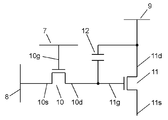
- FIG. 2 is an electric circuit diagram showing a circuit configuration of a pixel circuit for driving the pixel.
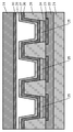
- FIG. 3 is a cross-sectional view showing a cross-sectional structure of the RGB sub-pixel portion in the EL display device.
- FIG. 4 is a diagram illustrating a schematic configuration of a plasma CVD apparatus for forming a sealing layer in a method for manufacturing an EL display device according to an embodiment of the present technology.
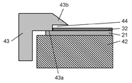
- FIG. 5 is an enlarged view of a portion A in FIG.
- FIG. 1 is a perspective view showing a schematic configuration of an organic EL display device according to an embodiment of the present technology
- FIG. 2 is a diagram showing a circuit configuration of a pixel circuit for driving a pixel.
- the EL display device includes a thin film transistor array device 1 in which a plurality of thin film transistors are arranged from the lower layer, an anode 2 as a lower electrode, a light emitting layer 3 made of an organic material, and a transparent upper electrode.
- the light emitting part is configured to have a laminated structure with a light emitting part composed of the cathode 4, and the light emitting part is controlled by the thin film transistor array device 1.
- the light emitting part has a configuration in which a light emitting layer 3 is disposed between a pair of electrodes, an anode 2 and a cathode 4, and a hole transport layer is formed between the anode 2 and the light emitting layer 3 so as to emit light.
- An electron transport layer is laminated between the layer 3 and the transparent cathode 4.
- the thin film transistor array device 1 has a plurality of pixels 5 arranged in a matrix.
- the thin film transistor array device 1 includes a plurality of gate wirings 7 arranged in a row, a plurality of signal wirings 8 arranged in a row so as to cross the gate wirings 7, and a parallel to the source wiring 8. And a plurality of power supply wires 9 (not shown in FIG. 1).
- the gate wiring 7 connects the gate electrode 10g of the thin film transistor 10 operating as a switching element included in each pixel circuit 6 for each row.
- the source wiring 8 connects the source electrodes 10 s of the thin film transistors 10 that operate as switching elements included in each of the pixel circuits 6 for each column.
- the power supply wiring 9 connects the drain electrode 11d of the thin film transistor 11 operating as a driving element included in each of the pixel circuits 6 for each column.
- the pixel circuit 6 includes a thin film transistor 10 that operates as a switching element, a thin film transistor 11 that operates as a driving element, and a capacitor 12 that stores data to be displayed on the corresponding pixel.
- the thin film transistor 10 includes a gate electrode 10g connected to the gate wiring 7, a source electrode 10s connected to the source wiring 8, a drain electrode 10d connected to the gate electrode 11g of the capacitor 12 and the thin film transistor 11, and a semiconductor film (FIG. Not shown).
- the thin film transistor 10 stores the voltage value applied to the source wiring 8 in the capacitor 12 as display data.
- the thin film transistor 11 includes a gate electrode 11g connected to the drain electrode 10d of the thin film transistor 10, a drain electrode 11d connected to the power supply wiring 9 and the capacitor 12, a source electrode 11s connected to the anode 2, and a semiconductor film (not shown). Z).
- the thin film transistor 11 supplies a current corresponding to the voltage value held by the capacitor 12 from the power supply wiring 9 to the anode 2 through the source electrode 11s. That is, the EL display device having the above configuration employs an active matrix system in which display control is performed for each pixel 5 located at the intersection of the gate line 7 and the source line 8.
- the light-emitting portion that emits at least red, green, and blue light-emitting colors has a matrix of a plurality of sub-pixels having at least red (R), green (G), and blue (B) light-emitting layers.
- a plurality of pixels are formed in an array.
- the sub-pixels constituting each pixel are separated from each other by a bank.
- This bank is provided by forming a ridge extending in parallel with the gate wiring 7 and a ridge extending in parallel with the source wiring 8 so as to intersect each other.
- a subpixel having an RGB light emitting layer is formed in a portion surrounded by the protrusions, that is, an opening of the bank.
- FIG. 3 is a cross-sectional view showing the cross-sectional structure of the RGB sub-pixel portion in the EL display device.
- a thin film transistor array device 22 constituting the pixel circuit 6 described above is formed on a base substrate 21 such as a glass substrate or a flexible resin substrate.
- an anode 23 which is a lower electrode, is formed through a planarization insulating film (not shown).
- a hole transport layer 24, an RGB light emitting layer 25 made of an organic material, an electron transport layer 26, and a cathode 27, which is a transparent upper electrode, are sequentially stacked.
- An EL light emitting unit is configured.
- the light emitting layer 25 of the light emitting part is formed in a region partitioned by the bank 28 which is an insulating layer.
- the bank 28 is for ensuring insulation between the anode 23 and the cathode 27 and partitioning the light emitting region into a predetermined shape, and is made of, for example, a photosensitive resin such as silicon oxide or polyimide.
- the hole transport layer 24 and the electron transport layer 26 are shown, but the hole transport layer 24 and the electron transport layer 26 are laminated with a hole injection layer and an electron injection layer, respectively. Is formed.
- the light emitting portion configured in this manner is covered with a sealing layer 29 such as silicon nitride, and further, a sealing substrate such as a transparent glass substrate or flexible resin substrate via an adhesive layer 30 on the sealing layer 29. 31 is sealed by being bonded over the entire surface.
- a sealing layer 29 such as silicon nitride
- a sealing substrate such as a transparent glass substrate or flexible resin substrate via an adhesive layer 30 on the sealing layer 29. 31 is sealed by being bonded over the entire surface.
- the shape, material, size and the like of the base substrate 21 are not particularly limited, and can be appropriately selected according to the purpose.
- a glass material such as alkali-free glass or soda glass, a silicon substrate, or a metal substrate may be used.
- Polyethylene terephthalate, polycarbonate, polyethylene naphthalate, polyamide, polyimide, etc. are suitable as the polymer material, but other known polymers such as acetate resin, acrylic resin, polyethylene, polypropylene, polyvinyl chloride resin, etc.
- a substrate material may be used.
- an organic EL light emitting element is formed after forming a polymer substrate on a rigid base material such as glass by a coating method or pasting, and then a rigid material such as glass is formed.
- a manufacturing method is used to remove a substrate.
- the anode 23 is a metal material having good electrical conductivity such as aluminum, aluminum alloy or copper, or a metal oxide or metal sulfide having high electrical conductivity such as light-transmitting IZO, ITO, tin oxide, indium oxide or zinc oxide. Etc.
- a thin film forming method such as a vacuum deposition method, a sputtering method, or an ion plating method is used.
- a polyvinyl carbazole material, a polysilane material, a polysiloxane derivative, a phthalocyanine compound such as copper phthalocyanine, an aromatic amine compound, or the like is used.
- a film forming method various coating methods can be used, and the film is formed to a thickness of about 10 nm to 200 nm.
- the hole injection layer stacked on the hole transport layer 24 is a layer that enhances hole injection from the anode 23, and is a metal oxide such as molybdenum oxide, vanadium oxide, or aluminum oxide, metal nitride, or metal oxide. Nitride is formed by sputtering.
- the light emitting layer 25 is mainly composed of an organic material that emits fluorescence, phosphorescence, and the like, and a dopant is added as necessary to improve the characteristics.
- a dopant is added as necessary to improve the characteristics.
- a high molecular weight organic material suitable for the printing method a polyvinyl carbazole derivative, a polyparaphenylin derivative, a polyfluorene derivative, a polyphenylene vinylene derivative, or the like is used.
- the dopant is used for shifting the emission wavelength and improving the light emission efficiency, and many dye-based and metal complex-based dopants have been developed.
- a printing method is suitable. Among various printing methods, an ink jet method is used, and the light emitting layer 25 having a thickness of about 20 nm to 200 nm is formed.
- the electron transport layer 26 is made of a material such as a benzoquinone derivative, a polyquinoline derivative, or an oxadiazole derivative.
- a film forming method a vacuum deposition method or a coating method is used, and the film is usually formed to a thickness of about 10 nm to 200 nm.
- the electron injection layer is made of a material such as barium, phthalocyanine, or lithium fluoride, and is formed by a vacuum deposition method or a coating method.
- the material of the cathode 27 differs depending on the light extraction direction.
- a light-transmitting conductive material such as ITO, IZO, tin oxide, or zinc oxide is used.
- materials such as platinum, gold, silver, copper, tungsten, aluminum, and aluminum alloy are used.
- a film forming method a sputtering method or a vacuum evaporation method is used, and the film is formed to a thickness of about 50 nm to 500 nm.
- the bank 28 is a structure necessary for filling a sufficient amount of a solution containing the material of the light emitting layer 25 in the region, and is formed in a predetermined shape by a photolithography method.
- the shape of the sub-pixels of the organic EL light emitting unit can be controlled by the shape of the bank 28.
- the sealing layer 29 is formed by forming a silicon nitride film, and a CVD (chemical vapor deposition) method is used as a film forming method.
- CVD chemical vapor deposition
- FIG. 4 is a diagram illustrating a schematic configuration of a plasma CVD apparatus for forming a sealing layer in the method for manufacturing an EL display device according to an embodiment of the present technology.
- the CVD apparatus introduces a reaction gas into the vacuum processing tank 41 and seals it on the panel portion 32 of the base substrate 21 disposed on the susceptor 42 by a CVD method through a mask 43.
- a silicon nitride film is formed as the stop layer 29.
- the panel section 32 is composed of a light emitting section on the base substrate 21 and a thin film transistor array device. In the configuration shown in FIG. 3, panel components up to the cathode 27 are formed.
- the CVD apparatus includes a mask support mechanism, a CCD camera, an alignment control unit, and the like in addition to the above-described components.
- the mask 43 is separated from the base substrate 21.
- an image of the overlapping portion of the base substrate 21 and the mask 43 is captured by the CCD camera, and the driving unit is operated based on the result obtained from the alignment control unit to align the mask 43.
- FIG. 5 is an enlarged view of part A of FIG. Specifically, in the method for manufacturing an EL display device according to an embodiment of the present technology, a schematic cross-sectional view illustrating a state in which a mask is aligned and installed on a base substrate disposed on a susceptor.
- the mask 43 has a gap 44 between the panel portion 32 and the contact portion 43 a that contacts the end portion of the base substrate 21 disposed on the susceptor 42. And an end 43b to be arranged. That is, the mask 43 is configured to be installed on the base substrate 21 with a gap 44 provided between the mask 43 and the panel unit 32 during film formation.
- the top emission type which is a structure that can easily achieve higher definition, is used, but the present technology is also effective for the bottom emission structure.
- the above embodiment has been described as an example of the present technology.
- the present technology is not limited to this, and can be applied to embodiments in which changes, replacements, additions, omissions, and the like are made.
Landscapes
- Chemical & Material Sciences (AREA)
- Engineering & Computer Science (AREA)
- Physics & Mathematics (AREA)
- Optics & Photonics (AREA)
- General Chemical & Material Sciences (AREA)
- Chemical Kinetics & Catalysis (AREA)
- Materials Engineering (AREA)
- Mechanical Engineering (AREA)
- Metallurgy (AREA)
- Organic Chemistry (AREA)
- Manufacturing & Machinery (AREA)
- Electroluminescent Light Sources (AREA)
Abstract
複数個の画素を配列して配置した発光部と、発光部の発光を制御する薄膜トランジスタアレイ装置とを備え、基板上に、発光部と薄膜トランジスタアレイ装置からなるパネル部を形成した後、パネル部を封止層により被覆するEL表示装置の製造方法において、封止層を形成する工程は、ベース基板(21)上にマスク(43)を配置して封止層を形成する膜を成膜することにより実施し、かつマスク(43)は、ベース基板(21)に当接する当接部(43a)と、パネル部(32)との間にギャップ(44)をあけて配置される端部(43b)とを有している。
Description
本技術は、EL表示装置の製造方法に関するものである。
近年、次世代の表示装置が盛んに開発されており、駆動用基板に、第1電極、発光層を含む複数の有機層および第2電極を順に積層したEL(Electroluminescence)表示装置が注目されている。EL表示装置は、自発光型であるので視野角が広く、バックライトを必要としないので省電力が期待でき、応答性が高く、装置の厚みを薄くできるなどの特徴を有している。そのため、テレビ等の大画面表示装置への応用が強く望まれている。
カラーディスプレイ用としては赤と青と緑の三色の画素による表示が最も一般的であり、省電力化や信頼性などを目的として赤と青と緑と白や赤と青と緑と薄青などの四色の画素による表示技術も各社で開発が進んでいる。
有機EL発光素子においては画素ごとに赤と青と緑の三色や赤と青と緑と白などの四色に有機EL発光部を形成する必要がある。
個別の有機EL部を形成する工法として最も一般的な工法は微細な穴の開いたファインメタルマスクを用いて、穴の部分だけに蒸着により有機EL部を形成する工法である。例えば、赤用ファインメタルマスクにより赤色に発色する有機EL部を蒸着により形成し、緑用ファインメタルマスクにより緑色に発色する有機EL部を蒸着により形成し、青用ファインメタルマスクにより青色に発色する有機EL部を蒸着により形成して、赤と緑と青の発光部が形成される。
一方大型の有機EL発光素子の作成やコストダウンには大型基板による有機EL発光素子技術の開発が重要である。
近年、大型基板による有機EL発光素子を形成する方法として二つの方法が注目されている。
一つ目の工法は白色有機EL素子を表示領域全域に形成し、赤と緑と青と白の四色のカラーフィルターにより着色表示させる方法である。この方法は大画面を形成したり、高精細ディスプレイを作成したりするには有効な方法である。
大型基板による有機EL発光素子の形成方法として注目されているもうひとつの工法は、塗布法により有機EL発光部を形成する方法である。塗布法としては様々な工法が検討されてきたが、大きく分けると凸版印刷やフレキソ印刷やスクリーン印刷やグラビア印刷などを用いるものとインクジェット法を用いるものである(特許文献1参照)。
本技術は、複数個の画素を配列して配置した発光部と、発光部の発光を制御する薄膜トランジスタアレイ装置とを備え、基板上に、発光部と薄膜トランジスタアレイ装置からなるパネル部を形成した後、パネル部を封止層により被覆するEL表示装置の製造方法において、封止層を形成する工程は、基板上にマスクを配置して封止層を形成する膜を成膜することにより実施し、かつマスクは、基板に当接する当接部と、パネル部との間にギャップをあけて配置される端部とを有していることを特徴とする。
本技術によれば、EL表示装置を製造する際に、歩留まりを向上させることが可能となる。
以下、本技術の一実施の形態によるEL表示装置の製造方法について、図1~図5の図面を用いて説明する。但し、必要以上に詳細な説明は省略する場合がある。例えば、既によく知られた事項の詳細説明や実質的に同一の構成に対する重複説明を省略する場合がある。これは、以下の説明が不必要に冗長になるのを避け、当業者の理解を容易にするためである。
なお、添付図面および以下の説明は、当業者が本開示を十分に理解するために、提供されるのであって、これらにより請求の範囲に記載の主題を限定することは意図されていない。
図1は本技術の一実施の形態による有機EL表示装置の概略構成を示す斜視図、図2は画素を駆動する画素回路の回路構成を示す図である。
図1、図2に示すように、EL表示装置は、下層より、複数個の薄膜トランジスタを配置した薄膜トランジスタアレイ装置1と、下部電極である陽極2、有機材料からなる発光層3及び透明な上部電極である陰極4からなる発光部との積層構造により構成され、発光部は薄膜トランジスタアレイ装置1により発光制御される。また、発光部は、一対の電極である陽極2と陰極4との間に発光層3を配置した構成であり、陽極2と発光層3の間には正孔輸送層が積層形成され、発光層3と透明な陰極4の間には電子輸送層が積層形成されている。薄膜トランジスタアレイ装置1には、複数の画素5がマトリックス状に配置されている。
各画素5は、それぞれに設けられた画素回路6によって駆動される。また、薄膜トランジスタアレイ装置1は、行状に配置される複数のゲート配線7と、ゲート配線7と交差するように列状に配置される複数の信号配線としてのソース配線8と、ソース配線8に平行に延びる複数の電源配線9(図1では省略)とを備える。
ゲート配線7は、画素回路6のそれぞれに含まれるスイッチング素子として動作する薄膜トランジスタ10のゲート電極10gを行毎に接続する。ソース配線8は、画素回路6のそれぞれに含まれるスイッチング素子として動作する薄膜トランジスタ10のソース電極10sを列毎に接続する。電源配線9は、画素回路6のそれぞれに含まれる駆動素子として動作する薄膜トランジスタ11のドレイン電極11dを列毎に接続する。
図2に示すように、画素回路6は、スイッチ素子として動作する薄膜トランジスタ10と、駆動素子として動作する薄膜トランジスタ11と、対応する画素に表示するデータを記憶するキャパシタ12とで構成される。
薄膜トランジスタ10は、ゲート配線7に接続されるゲート電極10gと、ソース配線8に接続されるソース電極10sと、キャパシタ12及び薄膜トランジスタ11のゲート電極11gに接続されるドレイン電極10dと、半導体膜(図示せず)とで構成される。この薄膜トランジスタ10は、接続されたゲート配線7及びソース配線8に電圧が印加されると、当該ソース配線8に印加された電圧値を表示データとしてキャパシタ12に保存する。
薄膜トランジスタ11は、薄膜トランジスタ10のドレイン電極10dに接続されるゲート電極11gと、電源配線9及びキャパシタ12に接続されるドレイン電極11dと、陽極2に接続されるソース電極11sと、半導体膜(図示せず)とで構成される。この薄膜トランジスタ11は、キャパシタ12が保持している電圧値に対応する電流を電源配線9からソース電極11sを通じて陽極2に供給する。すなわち、上記構成のEL表示装置は、ゲート配線7とソース配線8との交点に位置する画素5毎に表示制御を行うアクティブマトリックス方式を採用している。
また、EL表示装置において、少なくとも赤色、緑色および青色の発光色で発光する発光部は、少なくとも赤色(R)、緑色(G)、青色(B)の発光層を有するサブピクセルが複数個マトリクス状に配列されて複数個の画素が形成されている。各画素を構成するサブピクセルは、バンクによって互いに分離されている。このバンクは、ゲート配線7に平行に延びる突条と、ソース配線8に平行に延びる突条とが互いに交差するように形成することにより設けられる。そして、この突条で囲まれる部分、すなわちバンクの開口部にRGBの発光層を有するサブピクセルが形成されている。
図3は、EL表示装置において、RGBのサブピクセル部分の断面構造を示す断面図である。図3に示すように、EL表示装置は、ガラス基板、フレキシブル樹脂基板などのベース基板21上に、上述した画素回路6を構成する薄膜トランジスタアレイ装置22を形成している。また、薄膜トランジスタアレイ装置22には、平坦化絶縁膜(図示せず)を介して下部電極である陽極23が形成されている。そして、陽極23上には、正孔輸送層24、有機材料からなるRGBに発光する発光層25、電子輸送層26、透明な上部電極である陰極27が順に積層形成され、これによりRGBの有機EL発光部が構成されている。
また、発光部の発光層25は、絶縁層であるバンク28により区画された領域に形成されている。バンク28は、陽極23と陰極27との絶縁性を確保するとともに、発光領域を所定の形状に区画するためのものであり、例えば酸化シリコンまたはポリイミドなどの感光性樹脂により構成されている。
なお、上記実施の形態においては、正孔輸送層24、電子輸送層26のみを示しているが、正孔輸送層24、電子輸送層26それぞれには、正孔注入層、電子注入層が積層形成されている。
このように構成された発光部は、窒化ケイ素などの封止層29により被覆され、さらにこの封止層29上に接着層30を介して透明なガラス基板、フレキシブル樹脂基板などの封止用基板31が全面にわたって貼り合わされることにより封止されている。
ここで、ベース基板21としては、その形状、材質、大きさ等については、特に制限はなく、目的に応じて適宜選択することができる。例えば、無アルカリガラス、ソーダガラスなどのガラス材料やシリコン基板でも金属基板でも良い。また、軽量化やフレキシブル化を目的として高分子系材料を用いても良い。高分子系材料としては、ポリエチレンテレフタレート、ポリカーボネート、ポリエチレンナフタレート、ポリアミド、ポリイミドなどが適しているが、その他のアセテート系樹脂やアクリル系樹脂やポリエチレンやポリプロピレンやポリ塩化ビニル樹脂などの既知の高分子基板材料を用いても良い。高分子系材料を基板として用いるときには、ガラスなどの剛性のある基材の上に高分子基板を塗布法や貼り付けなどで形成した後、有機EL発光素子を形成し、その後ガラスなどの剛性のある基材を除去する製造方法が用いられる。
陽極23は、アルミニウムやアルミニウム合金や銅などの導電性の良い金属材料や、光透過性のIZO、ITO、酸化スズ、酸化インジウム、酸化亜鉛などの電気伝導度の高い金属酸化物や金属硫化物などにより構成される。成膜方法としては、真空蒸着法やスパッタリング法やイオンプレーティング法などの薄膜形成法が用いられる。
正孔輸送層24は、ポリビニルカルバゾール系材料、ポリシラン系材料、ポリシロキサン誘導体、銅フタロシアニンなどのフタロシアニン系化合物や芳香族アミン系化合物等などが用いられる。成膜方法としては、各種の塗布工法を用いることが可能であり、10nm~200nm程度の厚みに形成される。また、正孔輸送層24に積層される正孔注入層は、陽極23からの正孔注入を高める層であり、酸化モリブデンや酸化バナジウムや酸化アルミニウムなどの金属酸化物、金属窒化物、金属酸化窒化物をスパッタ法により形成される。
発光層25は、蛍光や燐光などを発光する有機系材料を主成分とし、必要に応じてドーパントを添加して特性を改善する。印刷法に適した高分子系有機材料としては、ポリビニルカルバゾール誘導体、ポリパラフェニリン誘導体、ポリフルオレン誘導体、ポリフェニレンビニレン誘導体などが用いられる。ドーパントは、発光波長のシフトや発光効率の改善のために用いられるものであり、色素系および金属錯体系のドーパントが数多く開発されている。また、大型基板に発光層25を形成する場合には印刷法が適しており、各種の印刷法の中でもインクジェット法が用いられ、20nm~200nm程度の厚みの発光層25が形成される。
電子輸送層26は、ベンゾキノン誘導体、ポリキノリン誘導体、オキサジアゾール誘導体などの材料が用いられる。成膜方法としては、真空蒸着法や塗布法が用いられ、通常10nm~200nm程度の厚みに形成される。また、電子注入層は、バリウム、フタロシアニン、フッ化リチウムなどの材料が用いられ、真空蒸着法や塗布法により形成される。
陰極27は、光の取り出し方向により材料が異なり、陰極27側から光を取り出す場合は、ITO、IZO、酸化スズ、酸化亜鉛などの光透光性の導電材料を用いる。陽極23側から光を取り出す場合は、白金、金、銀、銅、タングステン、アルミニウム及びアルミニウム合金などの材料を用いる。成膜方法としては、スパッタ法や真空蒸着法が用いられ、50nm~500nm程度の厚みに形成される。
バンク28は、領域内に発光層25の材料を含む溶液を十分な量で充填するために必要な構造物で、フォトリソ法によって所定の形状に形成される。バンク28の形状により、有機EL発光部のサブピクセルの形状を制御することができる。
封止層29は、窒化ケイ素膜を成膜することにより形成され、成膜法としてはCVD(化学気相成長)法が用いられる。
図4は、本技術の一実施の形態によるEL表示装置の製造方法において、封止層を成膜するためのプラズマCVD装置の概略構成を示す図である。図4に示すように、CVD装置は、真空処理槽41内に反応ガスを導入し、サセプタ42上に配置されたベース基板21のパネル部32上に、マスク43を介してCVD法により、封止層29としての窒化ケイ素膜を成膜するものである。パネル部32は、ベース基板21上の発光部と薄膜トランジスタアレイ装置から構成され、上記図3に示す構成において、陰極27までのパネル構成要素を形成したものである。
また、図示していないが、CVD装置は、上記構成部以外に、マスク支持機構、CCDカメラ、アライメント制御部などを備え、マスク43をアライメントするときは、マスク43をベース基板21から離間させた状態で、ベース基板21とマスク43との重なり部分の像をCCDカメラで取り込み、アライメント制御部から得られた結果に基づき、駆動部を動作させて、マスク43のアライメントを行う。
図5は、図4のA部の拡大図である。具体的には、本技術の一実施の形態によるEL表示装置の製造方法において、サセプタ上に配置されたベース基板にマスクをアライメントして設置した状態を示す概略断面図である。
図5に示すように、本技術においては、マスク43は、サセプタ42上に配置されたベース基板21の端部に当接する当接部43aと、パネル部32との間にギャップ44をあけて配置される端部43bとを有している。すなわち、マスク43は、成膜時、パネル部32との間にギャップ44を設けてベース基板21に設置されるように構成されている。
これにより、マスク43のアライメントを行い、ベース基板にマスク43を重ねて成膜を行うときに、ベース基板21のパネル部32にキズが発生するのを防止することができる。
なお、上記実施の形態においては、より高精細化を実現しやすい構造であるトップエミッション型で作成したが、本技術はボトムエミッション構造にも有効な技術である。
以上のように、本技術の例示として、上記の実施の形態を説明した。しかしながら、本技術は、これに限定されず、変更、置き換え、付加、省略などを行った実施の形態にも適用できる。
以上のように本技術によれば、EL表示装置を製造する際の歩留まりを向上させる上で有用である。
1,22 薄膜トランジスタアレイ装置
2,23 陽極
3,25 発光層
4,27 陰極
5 画素
6 画素回路
7 ゲート配線
8 ソース配線
9 電源配線
10,11 薄膜トランジスタ
21 ベース基板
24 正孔輸送層
26 電子輸送層
28 バンク
29 封止層
30 接着層
31 封止用基板
32 パネル部
41 真空処理槽
42 サセプタ
43 マスク
44 ギャップ
2,23 陽極
3,25 発光層
4,27 陰極
5 画素
6 画素回路
7 ゲート配線
8 ソース配線
9 電源配線
10,11 薄膜トランジスタ
21 ベース基板
24 正孔輸送層
26 電子輸送層
28 バンク
29 封止層
30 接着層
31 封止用基板
32 パネル部
41 真空処理槽
42 サセプタ
43 マスク
44 ギャップ
Claims (2)
- 複数個の画素を配列して配置した発光部と、前記発光部の発光を制御する薄膜トランジスタアレイ装置とを備え、基板上に、前記発光部と薄膜トランジスタアレイ装置からなるパネル部を形成した後、パネル部を封止層により被覆するEL表示装置の製造方法において、
前記封止層を形成する工程は、前記基板上にマスクを配置して封止層を形成する膜を成膜することにより実施し、かつ前記マスクは、前記基板に当接する当接部と、前記パネル部との間にギャップをあけて配置される端部とを有していることを特徴とするEL表示装置の製造方法。 - 前記封止層を形成する工程は、CVD法を用いて行うことを特徴とする請求項1に記載のEL表示装置の製造方法。
Priority Applications (2)
| Application Number | Priority Date | Filing Date | Title |
|---|---|---|---|
| JP2015513550A JPWO2014174804A1 (ja) | 2013-04-22 | 2014-04-16 | El表示装置の製造方法 |
| US14/584,997 US9293740B2 (en) | 2013-04-22 | 2014-12-29 | Method of manufacturing EL display device |
Applications Claiming Priority (2)
| Application Number | Priority Date | Filing Date | Title |
|---|---|---|---|
| JP2013-089022 | 2013-04-22 | ||
| JP2013089022 | 2013-04-22 |
Related Child Applications (1)
| Application Number | Title | Priority Date | Filing Date |
|---|---|---|---|
| US14/584,997 Continuation US9293740B2 (en) | 2013-04-22 | 2014-12-29 | Method of manufacturing EL display device |
Publications (1)
| Publication Number | Publication Date |
|---|---|
| WO2014174804A1 true WO2014174804A1 (ja) | 2014-10-30 |
Family
ID=51791393
Family Applications (1)
| Application Number | Title | Priority Date | Filing Date |
|---|---|---|---|
| PCT/JP2014/002158 Ceased WO2014174804A1 (ja) | 2013-04-22 | 2014-04-16 | El表示装置の製造方法 |
Country Status (3)
| Country | Link |
|---|---|
| US (1) | US9293740B2 (ja) |
| JP (1) | JPWO2014174804A1 (ja) |
| WO (1) | WO2014174804A1 (ja) |
Families Citing this family (2)
| Publication number | Priority date | Publication date | Assignee | Title |
|---|---|---|---|---|
| CN108231824B (zh) * | 2016-12-16 | 2024-04-23 | 京东方科技集团股份有限公司 | 一种oled显示面板及其制备方法 |
| CN113675247B (zh) * | 2021-07-29 | 2022-01-07 | 北京京东方技术开发有限公司 | 显示面板、显示面板的制造方法和显示装置 |
Citations (4)
| Publication number | Priority date | Publication date | Assignee | Title |
|---|---|---|---|---|
| JP2007005189A (ja) * | 2005-06-24 | 2007-01-11 | Tokki Corp | 有機膜形成用マスク,封止膜形成装置並びに封止膜の形成方法 |
| JP2007273274A (ja) * | 2006-03-31 | 2007-10-18 | Canon Inc | 有機el素子及びその製造方法 |
| JP2011076759A (ja) * | 2009-09-29 | 2011-04-14 | Toppan Printing Co Ltd | 有機エレクトロルミネッセンスパネルの製造方法およびパッシベーション層成膜用マスク |
| JP2011249301A (ja) * | 2010-05-28 | 2011-12-08 | Samsung Mobile Display Co Ltd | 有機発光表示装置およびその製造方法 |
Family Cites Families (2)
| Publication number | Priority date | Publication date | Assignee | Title |
|---|---|---|---|---|
| JP2011249089A (ja) | 2010-05-25 | 2011-12-08 | Panasonic Corp | 有機el表示パネルとその製造方法、および有機el表示装置 |
| JP2013109836A (ja) * | 2011-11-17 | 2013-06-06 | Mitsubishi Heavy Ind Ltd | 有機elパネルの製造方法及び有機elパネルの封止装置 |
-
2014
- 2014-04-16 JP JP2015513550A patent/JPWO2014174804A1/ja active Pending
- 2014-04-16 WO PCT/JP2014/002158 patent/WO2014174804A1/ja not_active Ceased
- 2014-12-29 US US14/584,997 patent/US9293740B2/en active Active
Patent Citations (4)
| Publication number | Priority date | Publication date | Assignee | Title |
|---|---|---|---|---|
| JP2007005189A (ja) * | 2005-06-24 | 2007-01-11 | Tokki Corp | 有機膜形成用マスク,封止膜形成装置並びに封止膜の形成方法 |
| JP2007273274A (ja) * | 2006-03-31 | 2007-10-18 | Canon Inc | 有機el素子及びその製造方法 |
| JP2011076759A (ja) * | 2009-09-29 | 2011-04-14 | Toppan Printing Co Ltd | 有機エレクトロルミネッセンスパネルの製造方法およびパッシベーション層成膜用マスク |
| JP2011249301A (ja) * | 2010-05-28 | 2011-12-08 | Samsung Mobile Display Co Ltd | 有機発光表示装置およびその製造方法 |
Also Published As
| Publication number | Publication date |
|---|---|
| US9293740B2 (en) | 2016-03-22 |
| JPWO2014174804A1 (ja) | 2017-02-23 |
| US20150118768A1 (en) | 2015-04-30 |
Similar Documents
| Publication | Publication Date | Title |
|---|---|---|
| WO2014136149A1 (ja) | El表示装置 | |
| US9536933B2 (en) | Display device having a light emitting layer on the auxiliary layer | |
| US20100193778A1 (en) | Organic light emitting diode display and method of manufacturing the same | |
| GB2430801A (en) | Dual substrate organic electroluminescent display | |
| KR20130093187A (ko) | 유기 발광 표시 장치 및 그 제조 방법 | |
| US9190624B2 (en) | Organic light emitting diode display | |
| JP2004101948A (ja) | 表示装置およびその製造方法 | |
| JP2015049949A (ja) | 有機el表示装置及び有機el表示装置の製造方法 | |
| JP6111487B2 (ja) | El表示装置 | |
| KR20110023996A (ko) | 유기전계발광 표시장치 | |
| WO2020056887A1 (zh) | 有机发光二极管显示屏及电子设备 | |
| US9502652B2 (en) | Method of manufacturing EL display device | |
| KR102242982B1 (ko) | 유기전계 발광표시장치 및 그 제조방법 | |
| US9293740B2 (en) | Method of manufacturing EL display device | |
| KR101717075B1 (ko) | 유기전기발광소자 | |
| US9209402B2 (en) | Method of manufacturing EL display device | |
| KR20080075262A (ko) | 유기전계발광표시장치 및 그 제조 방법 | |
| US9343710B2 (en) | Method of manufacturing EL display device | |
| WO2015087461A1 (ja) | 表示装置 | |
| US12593567B2 (en) | Organic light emitting display device and method for manufacturing the same | |
| JP2020027883A (ja) | 有機el表示装置および有機el表示装置の製造方法 | |
| KR101222985B1 (ko) | 유기 발광 소자 | |
| JP2004101945A (ja) | 表示装置 | |
| JP2014212087A (ja) | El表示装置の製造方法 |
Legal Events
| Date | Code | Title | Description |
|---|---|---|---|
| 121 | Ep: the epo has been informed by wipo that ep was designated in this application |
Ref document number: 14788198 Country of ref document: EP Kind code of ref document: A1 |
|
| ENP | Entry into the national phase |
Ref document number: 2015513550 Country of ref document: JP Kind code of ref document: A |
|
| NENP | Non-entry into the national phase |
Ref country code: DE |
|
| 122 | Ep: pct application non-entry in european phase |
Ref document number: 14788198 Country of ref document: EP Kind code of ref document: A1 |