WO2014171202A1 - 液晶表示装置 - Google Patents
液晶表示装置 Download PDFInfo
- Publication number
- WO2014171202A1 WO2014171202A1 PCT/JP2014/055434 JP2014055434W WO2014171202A1 WO 2014171202 A1 WO2014171202 A1 WO 2014171202A1 JP 2014055434 W JP2014055434 W JP 2014055434W WO 2014171202 A1 WO2014171202 A1 WO 2014171202A1
- Authority
- WO
- WIPO (PCT)
- Prior art keywords
- electrode
- liquid crystal
- substrate
- pixel
- display device
- Prior art date
- Legal status (The legal status is an assumption and is not a legal conclusion. Google has not performed a legal analysis and makes no representation as to the accuracy of the status listed.)
- Ceased
Links
Images


















Classifications
-
- G—PHYSICS
- G02—OPTICS
- G02F—OPTICAL DEVICES OR ARRANGEMENTS FOR THE CONTROL OF LIGHT BY MODIFICATION OF THE OPTICAL PROPERTIES OF THE MEDIA OF THE ELEMENTS INVOLVED THEREIN; NON-LINEAR OPTICS; FREQUENCY-CHANGING OF LIGHT; OPTICAL LOGIC ELEMENTS; OPTICAL ANALOGUE/DIGITAL CONVERTERS
- G02F1/00—Devices or arrangements for the control of the intensity, colour, phase, polarisation or direction of light arriving from an independent light source, e.g. switching, gating or modulating; Non-linear optics
- G02F1/01—Devices or arrangements for the control of the intensity, colour, phase, polarisation or direction of light arriving from an independent light source, e.g. switching, gating or modulating; Non-linear optics for the control of the intensity, phase, polarisation or colour
- G02F1/13—Devices or arrangements for the control of the intensity, colour, phase, polarisation or direction of light arriving from an independent light source, e.g. switching, gating or modulating; Non-linear optics for the control of the intensity, phase, polarisation or colour based on liquid crystals, e.g. single liquid crystal display cells
- G02F1/133—Constructional arrangements; Operation of liquid crystal cells; Circuit arrangements
- G02F1/1333—Constructional arrangements; Manufacturing methods
- G02F1/1343—Electrodes
- G02F1/134309—Electrodes characterised by their geometrical arrangement
- G02F1/134363—Electrodes characterised by their geometrical arrangement for applying an electric field parallel to the substrate, i.e. in-plane switching [IPS]
-
- G—PHYSICS
- G02—OPTICS
- G02F—OPTICAL DEVICES OR ARRANGEMENTS FOR THE CONTROL OF LIGHT BY MODIFICATION OF THE OPTICAL PROPERTIES OF THE MEDIA OF THE ELEMENTS INVOLVED THEREIN; NON-LINEAR OPTICS; FREQUENCY-CHANGING OF LIGHT; OPTICAL LOGIC ELEMENTS; OPTICAL ANALOGUE/DIGITAL CONVERTERS
- G02F1/00—Devices or arrangements for the control of the intensity, colour, phase, polarisation or direction of light arriving from an independent light source, e.g. switching, gating or modulating; Non-linear optics
- G02F1/01—Devices or arrangements for the control of the intensity, colour, phase, polarisation or direction of light arriving from an independent light source, e.g. switching, gating or modulating; Non-linear optics for the control of the intensity, phase, polarisation or colour
- G02F1/13—Devices or arrangements for the control of the intensity, colour, phase, polarisation or direction of light arriving from an independent light source, e.g. switching, gating or modulating; Non-linear optics for the control of the intensity, phase, polarisation or colour based on liquid crystals, e.g. single liquid crystal display cells
- G02F1/133—Constructional arrangements; Operation of liquid crystal cells; Circuit arrangements
- G02F1/1333—Constructional arrangements; Manufacturing methods
- G02F1/1335—Structural association of cells with optical devices, e.g. polarisers or reflectors
- G02F1/133528—Polarisers
-
- G—PHYSICS
- G02—OPTICS
- G02F—OPTICAL DEVICES OR ARRANGEMENTS FOR THE CONTROL OF LIGHT BY MODIFICATION OF THE OPTICAL PROPERTIES OF THE MEDIA OF THE ELEMENTS INVOLVED THEREIN; NON-LINEAR OPTICS; FREQUENCY-CHANGING OF LIGHT; OPTICAL LOGIC ELEMENTS; OPTICAL ANALOGUE/DIGITAL CONVERTERS
- G02F1/00—Devices or arrangements for the control of the intensity, colour, phase, polarisation or direction of light arriving from an independent light source, e.g. switching, gating or modulating; Non-linear optics
- G02F1/01—Devices or arrangements for the control of the intensity, colour, phase, polarisation or direction of light arriving from an independent light source, e.g. switching, gating or modulating; Non-linear optics for the control of the intensity, phase, polarisation or colour
- G02F1/13—Devices or arrangements for the control of the intensity, colour, phase, polarisation or direction of light arriving from an independent light source, e.g. switching, gating or modulating; Non-linear optics for the control of the intensity, phase, polarisation or colour based on liquid crystals, e.g. single liquid crystal display cells
- G02F1/133—Constructional arrangements; Operation of liquid crystal cells; Circuit arrangements
- G02F1/1333—Constructional arrangements; Manufacturing methods
- G02F1/1337—Surface-induced orientation of the liquid crystal molecules, e.g. by alignment layers
- G02F1/133707—Structures for producing distorted electric fields, e.g. bumps, protrusions, recesses, slits in pixel electrodes
-
- G—PHYSICS
- G02—OPTICS
- G02F—OPTICAL DEVICES OR ARRANGEMENTS FOR THE CONTROL OF LIGHT BY MODIFICATION OF THE OPTICAL PROPERTIES OF THE MEDIA OF THE ELEMENTS INVOLVED THEREIN; NON-LINEAR OPTICS; FREQUENCY-CHANGING OF LIGHT; OPTICAL LOGIC ELEMENTS; OPTICAL ANALOGUE/DIGITAL CONVERTERS
- G02F1/00—Devices or arrangements for the control of the intensity, colour, phase, polarisation or direction of light arriving from an independent light source, e.g. switching, gating or modulating; Non-linear optics
- G02F1/01—Devices or arrangements for the control of the intensity, colour, phase, polarisation or direction of light arriving from an independent light source, e.g. switching, gating or modulating; Non-linear optics for the control of the intensity, phase, polarisation or colour
- G02F1/13—Devices or arrangements for the control of the intensity, colour, phase, polarisation or direction of light arriving from an independent light source, e.g. switching, gating or modulating; Non-linear optics for the control of the intensity, phase, polarisation or colour based on liquid crystals, e.g. single liquid crystal display cells
- G02F1/133—Constructional arrangements; Operation of liquid crystal cells; Circuit arrangements
- G02F1/1333—Constructional arrangements; Manufacturing methods
- G02F1/1343—Electrodes
- G02F1/134309—Electrodes characterised by their geometrical arrangement
-
- G—PHYSICS
- G02—OPTICS
- G02F—OPTICAL DEVICES OR ARRANGEMENTS FOR THE CONTROL OF LIGHT BY MODIFICATION OF THE OPTICAL PROPERTIES OF THE MEDIA OF THE ELEMENTS INVOLVED THEREIN; NON-LINEAR OPTICS; FREQUENCY-CHANGING OF LIGHT; OPTICAL LOGIC ELEMENTS; OPTICAL ANALOGUE/DIGITAL CONVERTERS
- G02F1/00—Devices or arrangements for the control of the intensity, colour, phase, polarisation or direction of light arriving from an independent light source, e.g. switching, gating or modulating; Non-linear optics
- G02F1/01—Devices or arrangements for the control of the intensity, colour, phase, polarisation or direction of light arriving from an independent light source, e.g. switching, gating or modulating; Non-linear optics for the control of the intensity, phase, polarisation or colour
- G02F1/13—Devices or arrangements for the control of the intensity, colour, phase, polarisation or direction of light arriving from an independent light source, e.g. switching, gating or modulating; Non-linear optics for the control of the intensity, phase, polarisation or colour based on liquid crystals, e.g. single liquid crystal display cells
- G02F1/133—Constructional arrangements; Operation of liquid crystal cells; Circuit arrangements
- G02F1/1333—Constructional arrangements; Manufacturing methods
- G02F1/1343—Electrodes
- G02F1/13439—Electrodes characterised by their electrical, optical, physical properties; materials therefor; method of making
-
- G—PHYSICS
- G02—OPTICS
- G02F—OPTICAL DEVICES OR ARRANGEMENTS FOR THE CONTROL OF LIGHT BY MODIFICATION OF THE OPTICAL PROPERTIES OF THE MEDIA OF THE ELEMENTS INVOLVED THEREIN; NON-LINEAR OPTICS; FREQUENCY-CHANGING OF LIGHT; OPTICAL LOGIC ELEMENTS; OPTICAL ANALOGUE/DIGITAL CONVERTERS
- G02F1/00—Devices or arrangements for the control of the intensity, colour, phase, polarisation or direction of light arriving from an independent light source, e.g. switching, gating or modulating; Non-linear optics
- G02F1/01—Devices or arrangements for the control of the intensity, colour, phase, polarisation or direction of light arriving from an independent light source, e.g. switching, gating or modulating; Non-linear optics for the control of the intensity, phase, polarisation or colour
- G02F1/13—Devices or arrangements for the control of the intensity, colour, phase, polarisation or direction of light arriving from an independent light source, e.g. switching, gating or modulating; Non-linear optics for the control of the intensity, phase, polarisation or colour based on liquid crystals, e.g. single liquid crystal display cells
- G02F1/133—Constructional arrangements; Operation of liquid crystal cells; Circuit arrangements
- G02F1/1333—Constructional arrangements; Manufacturing methods
- G02F1/1335—Structural association of cells with optical devices, e.g. polarisers or reflectors
- G02F1/133528—Polarisers
- G02F1/133531—Polarisers characterised by the arrangement of polariser or analyser axes
-
- G—PHYSICS
- G02—OPTICS
- G02F—OPTICAL DEVICES OR ARRANGEMENTS FOR THE CONTROL OF LIGHT BY MODIFICATION OF THE OPTICAL PROPERTIES OF THE MEDIA OF THE ELEMENTS INVOLVED THEREIN; NON-LINEAR OPTICS; FREQUENCY-CHANGING OF LIGHT; OPTICAL LOGIC ELEMENTS; OPTICAL ANALOGUE/DIGITAL CONVERTERS
- G02F1/00—Devices or arrangements for the control of the intensity, colour, phase, polarisation or direction of light arriving from an independent light source, e.g. switching, gating or modulating; Non-linear optics
- G02F1/01—Devices or arrangements for the control of the intensity, colour, phase, polarisation or direction of light arriving from an independent light source, e.g. switching, gating or modulating; Non-linear optics for the control of the intensity, phase, polarisation or colour
- G02F1/13—Devices or arrangements for the control of the intensity, colour, phase, polarisation or direction of light arriving from an independent light source, e.g. switching, gating or modulating; Non-linear optics for the control of the intensity, phase, polarisation or colour based on liquid crystals, e.g. single liquid crystal display cells
- G02F1/133—Constructional arrangements; Operation of liquid crystal cells; Circuit arrangements
- G02F1/1333—Constructional arrangements; Manufacturing methods
- G02F1/1343—Electrodes
- G02F1/134309—Electrodes characterised by their geometrical arrangement
- G02F1/134345—Subdivided pixels, e.g. for grey scale or redundancy
Definitions
- the present invention relates to a liquid crystal display device. More specifically, the present invention relates to a horizontal electric field type liquid crystal display device.
- a liquid crystal display device is a device that controls transmission / blocking of light (display on / off) by controlling the orientation of liquid crystal molecules having birefringence.
- the liquid crystal alignment mode of the liquid crystal display device includes a TN (Twisted Nematic) mode in which liquid crystal molecules having positive dielectric anisotropy are aligned in a twisted state of 90 ° when viewed from the substrate normal direction, and a negative dielectric constant.
- VA Vertical alignment
- VA liquid crystal molecules having anisotropy are vertically aligned with respect to the substrate surface, and liquid crystal molecules having positive or negative dielectric anisotropy are horizontally aligned with respect to the substrate surface. Examples include an in-plane switching (IPS) mode in which a lateral electric field is applied to the layer and a fringe field switching (FFS) mode.
- IPS in-plane switching
- FFS fringe field switching
- an active matrix driving method is widely used in which an active element such as a thin film transistor (TFT) is arranged for each pixel to realize high image quality.
- TFT thin film transistor
- an array substrate including a plurality of TFTs and pixel electrodes, a plurality of scanning signal lines and a plurality of data signal lines are formed so as to intersect each other, and a TFT is provided at each of these intersections.
- the TFT is connected to the pixel electrode, and the supply of an image signal to the pixel electrode is controlled by the switching function of the TFT.
- the array substrate or the counter substrate is further provided with a common electrode, and a voltage is applied to the liquid crystal layer through the pair of electrodes.
- the pixel electrode and the common electrode are formed on the same substrate, and both electrodes are formed to have a plurality of comb teeth.
- the comb teeth of the pixel electrode and the comb teeth of the common electrode in one pixel are parallel to each other, and the orientation of the liquid crystal molecules is controlled based on the potential difference between the comb teeth of the pixel electrode and the comb teeth of the common electrode.
- the comb teeth of each electrode may be configured such that a part thereof is bent, whereby excellent viewing angle characteristics can be obtained (see, for example, Patent Documents 1 to 3).
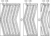
- FIG. 59 is a schematic plan view showing an example of electrode arrangement of a conventional IPS mode liquid crystal display device.
- a pixel electrode 111 and a common electrode 115 are arranged in one pixel, and each of them is a bent (V-shaped) comb.
- V-shaped bent
- the wide viewing angle characteristic can be obtained by arranging the longitudinal directions of the comb teeth of the electrodes 111 and 115 to be oblique with respect to the wirings.
- the pixel size is sufficiently large, even if a dark region occurs in some part, it is possible to obtain a bright display as a whole by supplementing the brightness in other regions, but as the pixel size decreases, Since the ratio of the area occupied by the dark region to the entire pixel becomes large, the influence of a decrease in transmittance appears more remarkably when the pixel has a higher definition.
- the present invention has been made in view of the above situation, and an object of the present invention is to provide a liquid crystal display device capable of obtaining good display characteristics even when the pixel size is reduced.
- the present inventors paid attention to the structure of the pixel electrode and the common electrode, and by simply changing the shape of the comb teeth of the pixel electrode and the common electrode as in the prior art, both high transmittance and wide viewing angle characteristics can be achieved. Judged difficult.
- attention is paid to the fact that one pixel is constituted by a combination of a pixel electrode and a common electrode each having a plurality of comb teeth, and when the substrate is viewed in plan view, Adjust the shape of each of the common electrodes so that they are partly square-shaped, and arrange these electrodes so that the inner lines of the corners of the pair of bowl-shaped electrodes face each other.
- the alignment of liquid crystal molecules is controlled by a pair of saddle-shaped electrodes.
- the present inventors provide a plurality of electrode pairs including a pair of saddle-shaped electrodes, and each saddle-like electrode included in each of two adjacent electrode pairs is connected to a wiring passing between each electrode pair as a reference axis. As shown in FIG. 3, the wirings are arranged symmetrically with each other and are connected to the saddle electrodes on the side close to the wiring, which are included in two adjacent electrode pairs. It was found that can be obtained.
- one aspect of the present invention includes a first substrate, a second substrate, and a liquid crystal layer sandwiched between the first substrate and the second substrate, the first substrate being independent from each other.
- a plurality of electrode pairs including a pair of saddle-shaped electrodes and a second bowl-shaped electrode, and the first bowl-shaped electrodes included in each of the two adjacent electrode pairs are connected to each other via the first connection wiring.
- the first saddle-shaped electrode and the second saddle-shaped electrode respectively included in are arranged so as to be symmetrical with respect to each other with the second connection wiring passing between each electrode pair as a reference axis,
- the inner line of the first saddle electrode and the second saddle electrode The the inner hull line, a liquid crystal display device which are opposed to each other.
- the liquid crystal display device includes a first substrate, a second substrate, and a liquid crystal layer sandwiched between the first substrate and the second substrate.
- the first substrate has a plurality of electrode pairs each including a first bowl-shaped electrode and a second bowl-shaped electrode which are independent from each other.
- An electric field is formed in the liquid crystal layer based on the potential difference between the first and second bowl-shaped electrodes. Then, the orientation of the liquid crystal molecules changes according to the strength of the electric field, the amount of light transmission is adjusted, and the on / off of the display is adjusted.
- the magnitude of the potential supplied to the first and second saddle-shaped electrodes is not particularly limited and can be appropriately adjusted depending on the design.
- the “saddle-shaped electrode” refers to an electrode having a bent part (corner part) and parts (end parts) located on both sides so as to sandwich the corner part. Further, when the first substrate is viewed in a plane, a line constituting the outer edge of the side (acute angle side) bent to the inside of the “saddle electrode” is referred to as an “inner line”, The line that forms the outer edge of the side that is bent outward (obtuse angle side) is referred to as the “outline”.
- the first saddle-shaped electrodes included in each of the two adjacent electrode pairs are connected to each other via a first connection wiring, and the second electrode included in each of the two adjacent electrode pairs.
- the saddle-shaped electrodes are connected to each other via the second connection wiring.
- the first and second saddle-shaped electrodes included in the two adjacent electrode pairs are symmetrical with respect to each other with the second connection wiring passing between the electrode pairs as a reference axis. It is arranged to be.
- a saddle-like electrode located farther than the second connection wiring is referred to as a “first saddle-like electrode”
- a saddle-like electrode located closer is referred to as a “second saddle-like electrode”. Electrode ".
- signals having the same potential are supplied to the first saddle-shaped electrodes included in the two electrode pairs adjacent to each other, and the second electrodes included in the two electrode pairs adjacent to each other are supplied. Signals having the same potential are supplied to the bowl-shaped electrodes.
- the electric field formed between each electrode pair can be symmetrical, and the wide field of view can be achieved without reducing the transmittance. Angular characteristics can be obtained.
- the configuration of the liquid crystal display device is not particularly limited by other components as long as such components are essential.
- an electrode different from the first and second saddle-shaped electrodes for example, third and fourth electrodes
- the other electrode is a saddle-shaped electrode.
- the second saddle-shaped electrode included in each of the two electrode pairs adjacent to each other and the second connection wiring are arranged on the same layer, and the second connection wiring is formed by planarizing the first substrate.
- the second saddle-like electrodes included in the two adjacent electrode pairs are disposed so as to fill in between the second electrode pairs, and the second electrode included in the two adjacent electrode pairs.
- the bowl-shaped electrode and the second connection wiring are preferably integrated. Thereby, it becomes an efficient arrangement configuration without an extra blank space, and contributes to the improvement of the aperture ratio.
- the tip of at least one end of the first saddle-shaped electrode is pointed when the first substrate is viewed in plan. It is more preferable that the tip of the end portion of the is sharp. Further, when the first substrate is viewed in plan, it is preferable that the tip of at least one end of the second bowl-shaped electrode is sharp, and the tips of both ends are sharp. Is more preferable. Thereby, the alignment disorder of the liquid crystal hardly occurs in the vicinity of the end portion of each saddle-shaped electrode, and thereby, highly uniform liquid crystal orientation can be obtained in the entire region surrounded by the pair of saddle-shaped electrodes.
- the inner line of the first saddle-shaped electrode is composed of at least three lines having different angles. Preferably it is.
- the inner lines of the second bowl-shaped electrode are composed of at least three lines having different angles. This makes it difficult for liquid crystal alignment to occur in the vicinity of the corners of each saddle-shaped electrode, whereby highly uniform liquid crystal alignment can be obtained in the entire region surrounded by the pair of saddle-shaped electrodes.
- any one of at least three lines having different angles of the first saddle-shaped electrode and the second saddle-shaped The electrode is preferably parallel to any one of at least three lines having different angles.
- the inner contour line of the first saddle-shaped electrode is curved when the first substrate is viewed in plan.
- the contour line of the second bowl-shaped electrode is curved. This makes it difficult for liquid crystal alignment to occur in the vicinity of the corners of each saddle-shaped electrode, whereby highly uniform liquid crystal alignment can be obtained in the entire region surrounded by the pair of saddle-shaped electrodes.
- the first saddle-like electrode and the second saddle-like electrode are the first saddle-like shape. It is preferable that they have a line-symmetric relationship with respect to a straight line passing between the electrode and the second saddle electrode. Thereby, the symmetry of the electric field formed by the pair of bowl-shaped electrodes is improved, and highly uniform liquid crystal alignment can be obtained.
- the first saddle-like electrode and the second saddle-like electrode are the first saddle-like shape. It is preferable that they have a point-symmetric relationship with respect to a point located between the electrode and the second saddle electrode. Thereby, the symmetry of the electric field formed by the pair of bowl-shaped electrodes is improved, and highly uniform liquid crystal alignment can be obtained.
- the first hook-shaped electrode and the second hook-shaped electrode are arranged on the same layer. Even when the first saddle-shaped electrode and the second saddle-shaped electrode are formed on different layers, it is possible to form a horizontal electric field, but the vertical component is partially included. In fact, an oblique electric field is formed. In this case, some liquid crystal molecules may rotate obliquely according to the electric field, thereby reducing the transmittance and viewing angle characteristics. By arranging the first saddle-shaped electrode and the second saddle-shaped electrode on the same layer, it becomes difficult to form such an oblique component electric field, so that a more uniform lateral electric field can be formed. It is possible to prevent a decrease in transmittance and viewing angle characteristics.
- the first substrate further includes a first polarizing plate
- the second substrate further includes a second polarizing plate, the polarization axis of the first polarizing plate, and the second polarizing plate
- the polarization axis is orthogonal, and when the first substrate is viewed in plan, the inner line of the first saddle-shaped electrode is the polarization axis of the first polarizing plate and the second polarization axis.
- the polarizing plate is disposed so as to form an angle with the polarization axis of the polarizing plate, and when the first substrate is viewed in plan, the inner line of the second bowl-shaped electrode is It is preferable that the polarizing plate is disposed so as to form an angle with the polarizing axis of the polarizing plate and the polarizing axis of the second polarizing plate. That is, in this embodiment, the first polarizing plate and the second polarizing plate are in a crossed Nicols arrangement relationship with each other. Since an electric field is formed between the first bowl-shaped electrode and the second bowl-shaped electrode, by adjusting the axis of each polarizing plate so as to form an angle with respect to the direction of the electric field, Good gradation display and white display can be obtained.
- the present invention it is possible to obtain a liquid crystal display device capable of obtaining good display characteristics even when the pixel size is reduced.
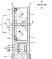
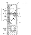
- FIG. 3 is a schematic plan view of a TFT substrate of the liquid crystal display device of Embodiment 1.
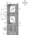
- FIG. FIG. 3 is a schematic plan view in which the position of a black matrix is added to the schematic plan view of the TFT substrate of Embodiment 1.
- FIG. 15 is a schematic cross-sectional view taken along the line AB in FIG. 3 or FIG. 14.
- FIG. 2 is a schematic diagram illustrating a configuration of a pixel assumed in Example 1 and represents a TFT substrate side.
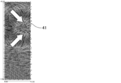
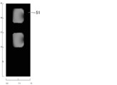
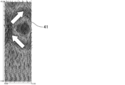
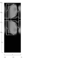
- Example 2 is a schematic diagram illustrating a configuration of a pixel assumed in Example 1 and represents a counter substrate side. It is an image showing the simulation result of Example 1, and represents a cross-sectional image when no voltage is applied (0 V). It is an image showing the simulation result of Example 1, and represents a planar image when no voltage is applied (0 V). It is an image showing the simulation result of Example 1, and represents the cross-sectional image at the time of white voltage application (9.7V). It is an image showing the simulation result of Example 1, and represents the planar image at the time of white voltage application (9.7V). In Example 1, it is the plane image which represented the light transmittance with the monochrome gradation. 3 is a graph showing viewing angle characteristics in Example 1.
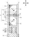
- FIG. 6 is a schematic plan view of a TFT substrate of a liquid crystal display device of Embodiment 2.
- FIG. It is a cross-sectional image showing the simulation image which shows the behavior of a liquid crystal molecule at the time of white voltage application (8.0V) of Example 2.
- It is a plane image showing the simulation image which shows the behavior of the liquid crystal molecule at the time of the white voltage application (8.0V) of Example 2.
- Example 2 it is the plane image which represented the light transmittance with the monochrome gradation.
- the black matrix in FIG. 17 is excluded, and the position of the electrode is added.
- 10 is a graph showing viewing angle characteristics in Example 2.
- 6 is a schematic plan view of a TFT substrate of a liquid crystal display device according to Embodiment 3.
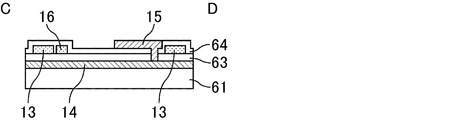
- Example 28 is a schematic sectional view taken along line CD in FIG. 20 or FIG. 27. It is a cross-sectional image showing the simulation image which shows the behavior of the liquid crystal molecule at the time of the white voltage application (8.4V) of Example 3. It is a plane image showing the simulation image which shows the behavior of the liquid crystal molecule at the time of the white voltage application (8.4V) of Example 3. In Example 3, it is the plane image which represented the light transmittance with the monochrome gradation. The black matrix in FIG. 24 is excluded, and the position of the electrode is added. 10 is a graph showing viewing angle characteristics in Example 3. 6 is a schematic plan view of a TFT substrate of a liquid crystal display device of Embodiment 4. FIG.
- Example 4 It is a cross-sectional image showing the simulation image which shows the behavior of the liquid crystal molecule at the time of the white voltage application (10.5V) of Example 4. It is a plane image showing the simulation image which shows the behavior of the liquid crystal molecule at the time of the white voltage application (10.5V) of Example 4. In Example 4, it is the plane image which represented the transmittance
- Example 5 It is a cross-sectional image showing the simulation image which shows the behavior of the liquid crystal molecule at the time of white voltage application (8.9V) of Example 5. It is a plane image showing the simulation image which shows the behavior of the liquid crystal molecule at the time of white voltage application (8.9V) of Example 5. In Example 5, it is the plane image which represented the light transmittance with the monochrome gradation. It is the plane image which excluded the black matrix in FIG. 37, and added the position of the electrode. 10 is a graph showing viewing angle characteristics in Example 5. 7 is a schematic plan view of a TFT substrate of a liquid crystal display device according to Embodiment 6. FIG.
- FIG. 10 is a graph showing viewing angle characteristics in Example 6.
- FIG. 10 is a schematic plan view of a TFT substrate of a liquid crystal display device according to a seventh embodiment.
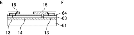
- FIG. 54 is a schematic sectional view taken along line EF in FIG. 46 or FIG.
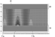
- FIG. 10 is a cross-sectional image showing a simulation image showing the behavior of liquid crystal molecules when white voltage is applied (10.8 V) in Example 7.
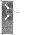
- FIG. It is a plane image showing the simulation image which shows the behavior of the liquid crystal molecule at the time of the white voltage application (10.8V) of Example 7.
- FIG. 51 is a planar image obtained by removing the black matrix in FIG. 50 and adding electrode positions.
- FIG. 10 is a graph showing viewing angle characteristics in Example 7.
- FIG. 10 is a schematic plan view of a TFT substrate of a liquid crystal display device according to an eighth embodiment.
- Example 8 It is a cross-sectional image showing the simulation image which shows the behavior of the liquid crystal molecule at the time of white voltage application (14.0V) of Example 8. It is a plane image showing the simulation image which shows the behavior of the liquid crystal molecule at the time of the white voltage application (14.0V) of Example 8. In Example 8, it is the plane image which represented the light transmittance with the monochrome gradation.
- FIG. 57 is a planar image obtained by removing the black matrix in FIG. 56 and adding electrode positions.
- FIG. 10 is a graph showing viewing angle characteristics in Example 8. It is a plane schematic diagram which shows an example of the electrode arrangement
- liquid crystal display devices of the following embodiments 1 to 8 are specifically applicable to televisions, personal computers, mobile phones, car navigation systems, information displays, and the like.
- a region in which the orientation of liquid crystal molecules is controlled by a pixel electrode controlled by one switching element and a common electrode facing the pixel electrode is defined as one “pixel”.
- the orientation of liquid crystal molecules is controlled by each of the plurality of pixel electrodes and each of the common electrodes facing each of the plurality of pixel electrodes. The entire area becomes one “pixel”.
- the effect of the present invention is noticeable when the pixel size is small.
- the present invention may be applied when the pixel size is large by providing a plurality of electrode pairs in one pixel.
- the pixel size that can efficiently obtain the effect of the present invention, there is a case where at least one side of the pixel is 20 ⁇ m or less, and further, 17 ⁇ m or less.
- electrode is a concept including so-called “wiring”.
- Embodiment 1 1 and 2 are schematic cross-sectional views of the liquid crystal display device of Embodiment 1.
- FIG. FIG. 1 shows the time when no voltage is applied
- FIG. 2 shows the time when a white voltage is applied.
- 3 and 4 are schematic plan views of the liquid crystal display device according to the first embodiment.
- FIG. 3 is a schematic plan view of the TFT substrate
- FIG. 4 is a schematic plan view of the TFT substrate with the position of the black matrix added.
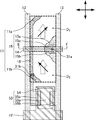
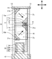
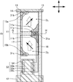
- FIG. 5 is a schematic sectional view taken along line AB in FIG.
- the liquid crystal display device of Embodiment 1 includes a TFT substrate (first substrate) 10, a counter substrate (second substrate) 20, and a liquid crystal layer 40 sandwiched between the TFT substrate 10 and the counter substrate 20.
- the liquid crystal layer 40 contains liquid crystal molecules 41 having negative dielectric anisotropy, and the liquid crystal molecules 41 are horizontal to the surfaces of the substrates 10 and 20 when no voltage is applied and when a voltage is applied. Oriented in various directions.
- the TFT substrate 10 includes a support substrate 61, a TFT (switching element) 53, a scanning signal line 12, a data signal line 13, a common signal line 14, a pixel electrode (first bowl-shaped electrode) 11, and a common electrode (second bowl).
- the counter substrate 20 includes a support substrate 62, a color filter, a black matrix, an alignment film, and the like.
- the pixel electrode 11 and the common electrode 15 are independent electrodes, and signals having different potentials are supplied to the pixel electrode 11 and the common electrode 15, respectively. Thereby, a voltage can be applied in the liquid crystal layer 40.
- the pixel electrode 11 is further divided into a first pixel electrode 11a and a second pixel electrode 11b.
- the first pixel electrode 11a and the second pixel electrode 11b are arranged on the same layer.
- the first pixel electrode 11a and the second pixel electrode 11b are connected to each other via a pixel electrode wiring (first connection wiring) 16, and each has an image signal (pixel potential) having the same potential. ) Is supplied.
- the pixel electrode wiring 16 is disposed on a layer different from the layer on which the first pixel electrode 11a and the second pixel electrode 11b are formed.
- the common electrode is further divided into a first common electrode 15a and a second common electrode 15b.
- the first common electrode 15a and the second common electrode 15b are arranged on the same layer.
- the first common electrode 15a and the second common electrode 15b are connected to each other via a common signal line (second connection wiring) 14, and a common signal having the same potential is supplied to each of them.
- the common signal line 14 is disposed so as to fill a space between the first common electrode 15a and the second common electrode 15b, whereby the first common electrode 15a, the second common electrode 15b, and
- the common signal line 14 is integrated.
- these are collectively referred to simply as a common electrode portion.
- the first pixel electrode 11a, the second pixel electrode 11b, the first common electrode 15a, and the second common electrode 15b are all disposed on the same layer. This makes it difficult to form an oblique electric field with respect to the substrate surface, so that a uniform lateral electric field can be formed, and deterioration of transmittance and viewing angle characteristics can be prevented.
- Examples of the member positioned in the lower layer include an insulating film formed on the support substrate 61.
- the insulating film may be formed of an organic material or an inorganic material, and may be a single film. There may be a plurality of films.
- a polarizing plate On the surface of the TFT substrate 10 opposite to the liquid crystal layer 40 side, a polarizing plate (first polarizing plate) is attached. A polarizing plate (second polarizing plate) is attached to the surface of the counter substrate 20 opposite to the liquid crystal layer 40 side.
- the first polarizing plate attached on the surface of the TFT substrate 10 and the second polarizing plate attached on the surface of the counter substrate 20 are arranged so that their polarization axes are orthogonal to each other. Yes.
- the first polarizing plate and the second polarizing plate have respective polarization axes that are the first pixel electrode 11a, the second pixel electrode 11b, the first common electrode 15a, and the second common electrode 15b. It arrange
- the scanning signal lines 12 and the data signal lines 13 are arranged so as to cross each other.
- a TFT (thin film transistor) 53 is provided near the contact point between the scanning signal line 12 and the data signal line 13.
- a common signal line 14 extending in parallel with the scanning signal line 12 is provided between the scanning signal lines 12.
- the orientation of the initial alignment of the liquid crystal molecules 41 is parallel to the extending direction of the data signal lines 13 and is orthogonal to the extending directions of the scanning signal lines 12 and the common signal lines 14.
- the double-headed arrow in FIG. 3 represents the direction of the polarization axis of the polarizing plate.
- each data signal line 13 and pixel electrode wiring 16 are formed on a support substrate 61.
- each data signal line 13 and the pixel electrode wiring 16 can be simultaneously formed using the same kind of wiring material.
- a first insulating film 63 is formed on the data signal line 13, the pixel electrode wiring 16 and the support substrate 61.
- the common signal line 14 is disposed on the first insulating film 63.
- the TFT 53 is a switching element including a semiconductor layer 54, a gate electrode 55a, a source electrode 55b, and a drain electrode 55c.
- a part of the scanning signal line 12 is used as it is for the gate electrode 55a.
- the source electrode 55 b is branched from the data signal line 13.
- the gate electrode 55a and the semiconductor layer 54 overlap each other with a gate insulating film interposed therebetween.
- the source electrode 55 b is connected to the drain electrode 55 c through the semiconductor layer 54.
- the pixel electrode wiring 16 is drawn out from the drain electrode 55c, and each of the first pixel electrode 11a and the second pixel electrode 11b is connected to the pixel via contact portions 31a and 31b penetrating the first insulating film 63.
- the electrode wiring 16 is connected to each other.
- the amount of current flowing through the semiconductor layer 54 is adjusted by a scanning signal input to the gate electrode 55a through the scanning signal line 12, and the source electrode 55b, the semiconductor layer 54, the drain electrode 55c, the pixel electrode wiring 16, through the data signal line 13 are adjusted. Transmission of the input image signal is controlled in the order of the first pixel electrode 11a or the second pixel electrode 11b.
- each of the first pixel electrode 11a and the second pixel electrode 11b has a bowl shape, and each has a line-symmetric shape with respect to an axis. Further, both the first pixel electrode 11a and the second pixel electrode 11b have pointed tips. Further, in both the first pixel electrode 11a and the second pixel electrode 11b, the inner line is composed of at least three lines (five lines in FIG. 3) having different angles, and is located in the middle. The line to be cut is orthogonal to the bisector (axisymmetric axis of symmetry) of each electrode.
- the first common electrode 15a and the second common electrode 15b are both bowl-shaped, and each has a line-symmetric shape with respect to a certain axis.
- both the first common electrode 15a and the second common electrode 15b have pointed ends.
- the inner line of each of the first common electrode 15a and the second common electrode 15b is composed of at least three lines (five lines in FIG. 3) having different angles, and is located in the middle. The line to be cut is orthogonal to the bisector (axisymmetric axis of symmetry) of each electrode.
- the first pixel electrode 11 a and the first common electrode 15 a are opposed to each other, and the respective contour lines have portions parallel to each other.
- the second pixel electrode 11b and the second common electrode 15b are opposed to each other in outline lines, and each outline line has a portion parallel to each other.
- the shape of the contour line is important for controlling the alignment of the liquid crystal molecules, and the shape of the contour line is not particularly limited.
- the first common electrode 15a and the second common electrode 15b are arranged so as to be line-symmetric with respect to each other with the common signal line 14 passing therebetween as a reference axis.
- the common signal line 14 is formed in a straight line regardless of pixel boundaries. That is, the common signal line 14 extends so as to cross each pixel, and one common signal line 14 corresponds to each of the common electrodes 15a and 15b included in the pixels arranged in the same direction as the extending direction. Supply the same common signal.
- the pixel electrode wiring 16 that connects the first pixel electrode 11 a and the second pixel electrode 11 b is formed to extend in parallel with the data signal line 13. That is, the pixel electrode wiring 16 is formed so as to intersect the common signal line 14.
- the first pixel electrode 11a, the second pixel electrode 11b, the first common electrode 15a, and the second common electrode 15b are all disposed on the same layer.
- the first common electrode 15a, the second common electrode 15b, and the common signal line 14 are all arranged on the same layer.
- the pixel electrode wiring 16 that connects the first pixel electrode 11a and the second pixel electrode 11b is disposed on a layer different from these electrodes. Thereby, it can prevent that each pixel electrode 11a, 11b and each common electrode 15a, 15b conduct
- the combination of the first pixel electrode 11a and the first common electrode 15a and the combination of the second pixel electrode 11b and the second common electrode 15b each constitute one set of electrode pairs.
- a plurality of such electrode pairs are formed on the TFT substrate 10.
- the combination of the first pixel electrode 11a and the first common electrode 15a is in a line-symmetric relationship with respect to a straight line passing between the electrodes 11a and 15a, and between the electrodes 11a and 15a. They are point-symmetric with respect to the point located.
- the combination of the second pixel electrode 11b and the second common electrode 15b is in a line symmetrical relationship with respect to a straight line passing between the electrodes 11b and 15b, and between the electrodes 11b and 15b. They are point-symmetric with respect to the point located.
- the first pixel electrode 11a, the second pixel electrode 11a, the second pixel electrode 11a, and the second pixel electrode 11b are symmetrical with respect to each other about a straight line passing between the first pixel electrode 11a and the second pixel electrode 11b.
- the arrangement of the pixel electrode 11b, the first common electrode 15a, and the second common electrode 15b is determined.
- only the shape or direction of the outline is different for each of the first pixel electrode 11a, the second pixel electrode 11b, the first common electrode 15a, and the second common electrode 15b. The dimensions are the same.
- each of the first pixel electrode 11a, the second pixel electrode 11b, the first common electrode 15a, and the second common electrode 15b (the length of the outline) Is different depending on the size of the pixel to be set, but is set in the range of 10 to 20 ⁇ m, for example. Further, the width of each of the first pixel electrode 11a, the second pixel electrode 11b, the first common electrode 15a, and the second common electrode 15b varies depending on the size and location of the pixel to be set. The part is set in a range of 2 ⁇ m.
- each pixel includes an outline of the first pixel electrode 11a, an extended line from both ends of the first pixel electrode 11a, an outline of the first common electrode 15a, A region surrounded by the extended lines from both ends of the common electrode 15a (hereinafter also referred to as the first divided region D1), the outline of the second pixel electrode 11b, and the second pixel electrode 11b A region surrounded by an extension line from both ends, a contour line of the second common electrode 15b, and an extension line from both ends of the second common electrode 15b (hereinafter also referred to as a second divided region D2). Is included.
- a region below the first divided region D1 and the second divided region D2 (hereinafter also referred to as a blank region D3) is also a part of the pixel.
- the area of the blank area D3 is approximately the same as the area of each of the first divided area D1 and the second divided area D2, but is not particularly limited, and is reduced as necessary. Can do.
- the first pixel electrode 11a is located at the upper left of the first divided region D1
- the first common electrode 15a is located at the lower right of the first divided region D1
- the second pixel electrode 11b is located at the upper right of the second divided region D2.
- the position is not particularly limited as long as the contour lines face each other.
- the scanning signal line 12 is formed in the blank area D3 below the pixel electrodes 11a and 11b and the common electrodes 15a and 15b.
- the scanning signal line 12 is also formed in a straight line regardless of the pixel boundary. That is, the scanning signal line 12 is extended so as to cross each pixel, and one scanning signal line 12 supplies the same scanning signal to the TFTs included in the pixels arranged in the same direction as the extending direction. is doing.
- the arrangement location of the scanning signal lines 12 is not particularly limited, and a design with a high degree of freedom is possible.
- the TFT 53 is formed in the blank region D3 below the pixel electrodes 11a and 11b and the common electrodes 15a and 15b.
- the arrangement location of the TFT 53 is not particularly limited, and a design with a high degree of freedom is possible. As will be described later, when an oxide semiconductor such as IGZO is used as the material of the semiconductor layer 54 of the TFT 53, the size of the entire TFT 53 can be reduced.
- the black matrix 51 is provided with openings in accordance with regions where the orientation of liquid crystal molecules is controlled by the respective electrodes. That is, the black matrix 51 is formed so that the outer edge of the opening is formed along the first divided region D1 and the second divided region D2. As a result, the black matrix 51 forms a lattice shape when viewed as a whole.
- the blank area D3 is covered with the black matrix 51.
- the plurality of openings formed so as to be surrounded by the black matrix 51 thus serve as a region that transmits display light.
- each corner of the opening of the black matrix 51 has an outline of the adjacent first pixel electrode 11a, first common electrode 15a, second pixel electrode 11b, or second common electrode 15b. It has a part parallel to. In other words, the shape of each of the openings is a polygon with chamfered square corners.
- the opening of the black matrix 51 is set slightly smaller than the first divided region D1 and the second divided region D2.
- the length of one side of the first divided region D1 and the second divided region D2 is not less than 110% and not less than one side of the opening formed along these.
- the liquid crystal molecules 41 are composed of the first pixel electrode 11a, the second pixel electrode 11b, the first common electrode 15a, and the second common electrode. It is oriented to form an angle with respect to each bisector of 15b. 3 and 4, the white dotted arrow indicates the orientation direction (major axis direction) of the liquid crystal molecules when no voltage is applied.
- the liquid crystal molecules are the first pixel electrode 11a, the second pixel electrode 11b, the first common electrode 15a, and the second common electrode.
- the electrodes 15b are oriented in directions parallel or perpendicular to the bisectors.
- the black arrows in FIGS. 3 and 4 indicate the orientation direction (major axis direction) of the liquid crystal molecules when a white voltage is applied.
- both the first divided region D1 and the second divided region D2 have a rectangular shape or a square shape as a whole. Thereby, excellent transmittance and wide viewing angle characteristics can be obtained.
- each electrode itself has a line-symmetric shape with respect to a certain axis
- the inner line of each electrode is composed of at least three lines having different angles, and the line located in the middle is orthogonal to the bisector of each electrode,
- Pixel The combination of the electrode and the common electrode has a symmetrical structure (specifically, line symmetry, point symmetry), (v) the electrode pair constituting the first divided region D1, and the second divided The electrode pair constituting the region D2 has a symmetrical structure (specifically, line symmetry), (vi) the size of each electrode constituting one pixel is the same, etc. It contributes to high transmittance and wide viewing angle characteristics.
- Example 1 are schematic diagrams illustrating the configuration of the pixel assumed in the first embodiment.
- FIG. 6 illustrates the TFT substrate side
- FIG. 7 illustrates the counter substrate side.
- the simulation conditions of Example 1 were set as follows.
- the pixel size was 15 ⁇ m ⁇ 45 ⁇ m.
- Each inner line of the pixel electrode and the common electrode is composed of five lines having different angles, and the angles formed by the lines are all obtuse. Thereby, the area
- the angle formed by the line positioned in the middle (hereinafter also referred to as the inner contour line of the corner) and the lines positioned on both sides thereof was 152 °.
- the distance between the pixel electrode and the common electrode (specifically, the length of a straight line connecting the innermost corner of the pixel electrode and the innermost corner of the common electrode) was 10.1 ⁇ m. .
- a margin of 2 ⁇ m was taken from the outer edge of the pixel to the outline of each electrode.
- the length of the vertical sides of the first divided region D1 and the second divided region D2 was 13 ⁇ m, and the length of the horizontal side was 11 ⁇ m. Therefore, the aspect ratio of each divided region D1 and D2 is 13:11.
- the size of the opening of the black matrix was 9 ⁇ m ⁇ 7 ⁇ m, and the four corners were chamfered with right-angled isosceles triangles having a base of 1 ⁇ m. That is, the aspect ratio of the black matrix opening is 9: 7.
- the pixel electrode and the common electrode are shaped like bowls, and are arranged in the vicinity of the corners of the openings so as to surround the openings of the black matrix with a certain interval, Controls the direction of the electric field in a desired direction while preventing the generation of a local electric field in a virtual region formed by being surrounded by the common electrode and a line formed by connecting the tips of these ends. be able to. Furthermore, by gradually changing the inclinations of the inner lines of the pixel electrode and the common electrode, the rate of change in the direction of the electric field can be reduced, and the occurrence of liquid crystal alignment disorder can be suppressed.
- FIG. 8 to 13 are images or graphs showing the simulation results of Example 1.
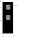
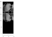
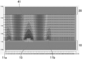
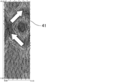
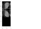
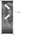
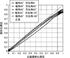
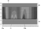
- FIG. As the liquid crystal material, a material having negative dielectric anisotropy is used. 8 and 9 show the case when no voltage is applied (0 V), and FIGS. 10 and 11 show the case when a white voltage is applied (9.7 V). 8 and 10 represent cross-sectional images, and FIGS. 9 and 11 represent planar images. 12 is a plane image in which light transmittance is expressed in monochrome gradation in Example 1, and FIG. 13 is a graph showing the viewing angle characteristics in Example 1, with the display screen as a reference plane. Each brightness is shown when the polar angle is fixed at 45 ° and the value of the azimuth is changed.
- the liquid crystal molecules 41 are uniformly aligned in the long side direction of the pixel.
- FIGS. 10 and 11 when a voltage higher than the threshold is applied, the initial alignment of the liquid crystal molecules 41 is maintained in the vicinity of the TFT substrate 10, but the alignment of the liquid crystal molecules 41 is changed in other cases.
- the liquid crystal molecules 41 positioned between the pixel electrodes 11a and 11b and the common electrodes 15a and 15b facing the pixel electrodes 11a and 11b have different angles depending on the distance from each electrode, but are oblique to the long side direction of the pixel. Oriented to face the direction of. In FIG. 10 and FIG. 11, each region is indicated by gradation according to the strength of the electric field.
- liquid crystal molecules included in the second divided region D2 have different angles depending on the region, most of them are orthogonal to the inner line of each electrode, that is, in a direction of about 45 ° with respect to the initial alignment.
- the angle change is smooth and uniform.
- a characteristic point here is that the alignment distribution (director distribution) of the liquid crystal molecules 41 passes between the first common electrode 15a and the second common electrode 15b, that is, a common signal line. This is a point that is line-symmetric with respect to the axis 14. Another feature is that even if the initial orientation direction is one direction, the orientation direction is automatically set in a different direction in a region corresponding to one pixel in the liquid crystal layer. As a result, two regions (multi-domains) including a plurality of liquid crystal molecules having a symmetrical alignment pattern around a certain reference axis can be formed.
- the alignment of the liquid crystal molecules can be made uniform in the portion used as the display region, and two regions having alignment orientations in different directions can be formed. Therefore, it is possible to efficiently use light and obtain excellent viewing angle characteristics.
- the configuration of the first embodiment even if the pixel size is designed to be small, an excellent effect that the characteristics are not deteriorated can be exhibited.
- the transmittance As shown in FIG. 12, it can be seen that light is uniformly transmitted through the entire area serving as the opening of the black matrix 51, and a high transmittance can be secured.
- the viewing angle characteristics As shown in FIG. 13, there is no great difference in luminance depending on the angle, and the end portion of each curve converges at the same place. Even if it is tilted, it can be seen that there is no change in appearance and that excellent viewing angle characteristics can be obtained.
- the aspect ratio of the first divided region D1 and the second divided region D2 and the aspect ratio of the opening of the black matrix 51 are not necessarily matched.
- the shape of the opening of the black matrix 51 may be determined according to a region suitable for display, and is not limited to a rectangle or a square. Further, the magnitude relationship between the size of the first divided region D1 and the second divided region D2 and the size of the opening of the black matrix 51 is not particularly limited.
- a transparent material such as glass or plastic is preferably used.
- a material of the insulating film for example, the first insulating film 63 and the second insulating film 64
- a transparent material such as silicon nitride, silicon oxide, or photosensitive acrylic resin is preferably used.
- a color filter may be disposed instead of these insulating films.
- a silicon nitride film is formed by a plasma-enhanced chemical vapor deposition (PECVD) method, and a photosensitive acrylic resin film is formed on the silicon nitride film by a die coating (coating) method. It is formed by film formation. Holes provided in each insulating film for forming the contact portions 31a, 31b, and 31c can be formed by performing dry etching (channel etching).
- the scanning signal line 12, the data signal line 13, the common signal line 14, the pixel electrode wiring 16, and the various electrodes constituting the TFT 53 are made of a metal such as titanium, chromium, aluminum, molybdenum, or the like by sputtering or the like.
- the alloy can be formed by depositing a single layer or a plurality of layers, followed by patterning by a photolithography method or the like.
- the same material is used to make the manufacturing more efficient.
- the common signal line 14 is formed integrally with the common electrode 15
- the same material may be used, thereby increasing the production efficiency.
- the same material may be used for the pixel electrode wiring 16 when the pixel electrode wiring 16 is formed integrally with the pixel electrode 11, for example, thereby increasing the production efficiency.
- the semiconductor layer 54 of the TFT 53 for example, a high resistance semiconductor layer (i layer) made of amorphous silicon, polysilicon or the like, and a low resistance semiconductor layer made of n + amorphous silicon or the like in which amorphous silicon is doped with an impurity such as phosphorus or the like ( n + layer), but the can be used as a laminate of, as the other, IGZO (indium - gallium - zinc - oxygen) oxide semiconductor such as is preferably used.
- IGZO indium - gallium - zinc - oxygen
- an oxide semiconductor such as IGZO as the material of the semiconductor layer 54, the electron mobility is high and the size of the TFT 53 can be reduced, so that a large aperture ratio can be secured. Therefore, an oxide semiconductor using IGZO is advantageous when reducing the size of a pixel. In addition, since the off-leakage characteristic is low, the charge can be held for a long time, and the advantage that low frequency driving is possible can be obtained.
- the pixel electrode 11 and the common electrode 15 are formed by sputtering a transparent conductive material such as indium tin oxide (ITO), indium zinc oxide (IZO), zinc oxide (ZnO), tin oxide (SnO), or an alloy thereof. After a single layer or a plurality of layers are formed by a method or the like, patterning can be performed using a photolithography method or the like.
- a transparent conductive material such as indium tin oxide (ITO), indium zinc oxide (IZO), zinc oxide (ZnO), tin oxide (SnO), or an alloy thereof.
- a photosensitive resin (color resist) that transmits light corresponding to each color is preferably used.
- the material of the black matrix 51 is not particularly limited as long as it has a light shielding property, and a resin material containing a black pigment or a metal material having a light shielding property is preferably used.
- the color filter and the black matrix 51 may be arranged not on the counter substrate 20 side but on the TFT substrate 10 side.
- the TFT substrate 10 and the counter substrate 20 manufactured in this way are provided with a plurality of columnar spacers made of an insulating material on one substrate, and then bonded to each other using a sealing material.
- a liquid crystal layer 40 is formed between the TFT substrate 10 and the counter substrate 20, but when the dropping method is used, the liquid crystal material is dropped before the substrates are bonded, and the vacuum injection method is used. The liquid crystal material is injected after the substrates are bonded.
- a liquid crystal display device is completed by affixing a polarizing plate, retardation film, etc. on the surface on the opposite side to the liquid crystal layer 40 side of each board
- Embodiment 2 The second embodiment is the same as the first embodiment except that the initial alignment direction of the liquid crystal molecules is different, the dielectric anisotropy of the liquid crystal material is different, and the shapes of the pixel electrode and the common electrode are different. . Specifically, the orientation of the initial alignment of the liquid crystal molecules in the second embodiment is set to be parallel to the extending directions of the scanning signal line and the common signal line. As the dielectric anisotropy of the liquid crystal material, a positive type is used.
- FIG. 14 is a schematic plan view of a TFT substrate of the liquid crystal display device according to the second embodiment. A cross-sectional view along the line AB in FIG. 14 is the same as FIG.
- Example 2 When simulation was performed assuming the liquid crystal display device of Embodiment 2, the following results were obtained (Example 2).
- the simulation conditions of Example 2 are the same as those of the simulation of Example 1 except for the orientation direction of liquid crystal molecules, the dielectric anisotropy of the liquid crystal material, and the shape of each electrode.
- the initial orientation is 90 ° different from that in Example 1, and what was set in the upward direction in Example 1 is set in the right direction. That is, in Example 2, the initial alignment direction of the liquid crystal molecules 41 is parallel to the extending directions of the scanning signal lines 12 and the common signal lines 14 and orthogonal to the extending direction of the data signal lines 13. Yes.
- each inner line of the pixel electrode and the common electrode is composed of five lines having different angles, and the angles formed by the lines are all obtuse. More specifically, among the five lines, the angle formed by the line positioned in the middle (hereinafter also referred to as the inner contour line of the corner) and the lines positioned on both sides thereof was 157 °.
- the distance between the pixel electrode and the common electrode (specifically, the length of a straight line connecting the innermost corner of the pixel electrode and the innermost corner of the common electrode) was 10.1 ⁇ m. .
- the optimal electrode shape varies depending on the initial orientation direction of the liquid crystal molecules to be used and the dielectric anisotropy of the liquid crystal material.
- FIG. 15 and 16 show simulation images showing the behavior of liquid crystal molecules when white voltage is applied (8.0 V) in Example 2, FIG. 15 is a cross-sectional image, and FIG. 16 is a planar image.
- FIG. 17 is a planar image in which light transmittance is expressed in monochrome gradation in Example 2, and FIG. 18 is obtained by excluding the black matrix in FIG. 17 and adding electrode positions.
- FIG. 19 is a graph showing viewing angle characteristics in Example 2, and represents each luminance when the polar angle is fixed at 45 ° and the value of the azimuth angle is changed with the display screen as a reference plane.
- the initial alignment of the liquid crystal molecules 41 is maintained in the vicinity of the TFT substrate 10, but the alignment of the liquid crystal molecules 41 is changed in other cases.
- the liquid crystal molecules 41 positioned between the pixel electrodes 11a and 11b and the common electrodes 15a and 15b facing the pixel electrodes 11a and 11b have different angles depending on the distance from each electrode, but are oblique to the long side direction of the pixel. It is oriented to face the direction.
- each region is indicated by gradation according to the strength of the electric field.
- the alignment distribution (director distribution) of the liquid crystal molecules 41 is a straight line passing between the first common electrode 15a and the second common electrode 15b, that is, These are symmetrical with respect to the common signal line 14 as an axis.
- two regions including a plurality of liquid crystal molecules having alignment orientations in different directions and having a symmetrical alignment pattern around a certain reference axis can be formed.
- the pixel electrode and the common electrode can be formed in a desired shape even if the orientation of the initial alignment and the dielectric anisotropy of the liquid crystal material are different. By doing so, similar characteristics can be obtained.
- two electrode pairs consisting of a pixel electrode and a common electrode are used, it is possible to form two regions with orientation orientations in different directions, efficiently using light, and excellent viewing angle characteristics Can be obtained. Further, even if the pixel size is designed to be small, an excellent effect that the characteristics are not deteriorated can be exhibited.
- the transmittance As shown in FIG. 17, it can be seen that light is uniformly transmitted through the entire region serving as the opening of the black matrix 51, and a high transmittance can be secured. Further, as shown in FIG. 18, even if the black matrix is not taken into consideration, a sufficiently wide transmission region occupying a certain range is formed. As shown in FIG. 19, the viewing angle characteristics are different in tendency, but as in Example 1, there is no significant difference in luminance depending on the angle, and the end portions of the curves converge to the same place. Therefore, it can be seen that the viewing angle does not change regardless of the viewing angle, and excellent viewing angle characteristics can be obtained.
- Embodiment 3 The third embodiment is the same as the second embodiment except that the shape of the common electrode and the pixel electrode, the common electrode, and the common signal line are provided on different layers.
- FIG. 20 is a schematic plan view of a TFT substrate of the liquid crystal display device according to the third embodiment.
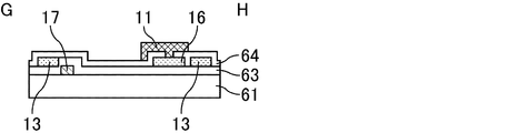
- FIG. 21 is a schematic cross-sectional view taken along the line CD of FIG.
- the common signal line 14 is formed on the support substrate 61.
- a first insulating film 63 is formed on the common signal line 14 and the support substrate 61.
- Each data signal line 13 and pixel electrode wiring 16 are arranged on the first insulating film 63.
- a second insulating film 64 is formed on each data signal line 13 and the pixel electrode wiring 16.
- the common electrode 15 is disposed on the second insulating film 64.
- the first common electrode 15a and the second common electrode 15b are not the common signal line 14 but the first common electrode. They are connected to each other via a connection electrode (second connection wiring) 15c located between 15a and the second common electrode 15b. That is, the first common electrode 15a, the second common electrode 15b, and the connection electrode 15c are integrated to form a common electrode portion.
- the common signal line 14 and the connection electrode 15 c are connected to each other via a contact portion 31 c that penetrates the first insulating film 63 and the second insulating film 64. Thereby, a common signal can be transmitted from the common signal line 14 to the first common electrode 15a and the second common electrode 15b via the connection electrode 15c.
- a step is likely to occur on the surface of the TFT substrate 10 as compared with the first and second embodiments because the electrodes and the wirings are arranged in different layers as described above. Yes.
- Example 3 When a specific simulation was actually performed assuming the liquid crystal display device of Embodiment 3, the following results were obtained (Example 3).
- the simulation conditions of Example 3 are the same as those of Example 2 except that the shape of the common electrode and the pixel electrode, the common electrode, and the common signal line are provided on different layers.
- 22 and 23 show simulation images showing the behavior of liquid crystal molecules when white voltage is applied in Example 3 (8.4 V: increase of 0.4 V compared to Example 2), and FIG. 22 is a cross-sectional image.
- FIG. 23 is a planar image.
- FIG. 24 is a planar image in which light transmittance is expressed in monochrome gradation in Example 3, and FIG. 25 is obtained by excluding the black matrix in FIG. 24 and adding electrode positions.
- FIG. 26 is a graph showing viewing angle characteristics in Example 3, and represents each luminance when the polar angle is fixed at 45 ° and the value of the azimuth angle is changed with the display screen as a reference plane.
- the initial alignment of the liquid crystal molecules 41 is maintained in the vicinity of the TFT substrate 10, but the alignment of the liquid crystal molecules 41 is changed in other cases.
- the liquid crystal molecules 41 positioned between the pixel electrodes 11a and 11b and the common electrodes 15a and 15b facing the pixel electrodes 11a and 11b have different angles depending on the distance from each electrode, but are oblique to the long side direction of the pixel. It is oriented to face the direction.
- each region is indicated by gradation according to the strength of the electric field.
- the orientation distribution (director distribution) of the liquid crystal molecules 41 is a straight line passing between the first common electrode 15a and the second common electrode 15b, that is, the connection electrode 15c or the common signal line.
- Axis 14 is symmetrical with respect to each other.
- the connection electrode 15c is formed for each pixel, but the common signal line 14 is formed in a straight line regardless of the boundary of the pixel.
- two regions including a plurality of liquid crystal molecules having alignment orientations in different directions and having a symmetrical alignment pattern around a certain reference axis Multidomain
- the pixel electrode and the common electrode are desired even if the pixel electrode, the common electrode, and the common signal line are provided on different layers.
- the same characteristics can be obtained.
- two electrode pairs consisting of a pixel electrode and a common electrode are used, it is possible to form two regions with orientation orientations in different directions, efficiently using light, and excellent viewing angle characteristics Can be obtained. Further, even if the pixel size is designed to be small, an excellent effect that the characteristics are not deteriorated can be exhibited.
- the transmittance As shown in FIG. 24, it can be seen that light is uniformly transmitted through the entire area of the black matrix 51, and a high transmittance can be secured. Further, as shown in FIG. 25, even if the black matrix is not taken into consideration, a sufficiently wide transmission region occupying a certain range is formed. Actually, there is a slight decrease in the transmittance (specifically, -1%) due to the difference in level on the surface of the TFT substrate compared to Example 2. I understood, but there is almost no effect. As shown in FIG. 26, the viewing angle characteristics are almost the same as those in the second embodiment, the luminance does not vary greatly depending on the angle, and the end portions of the curves converge at the same place. Thus, it can be seen that no matter what angle the viewing angle is tilted, there is no change in the appearance and excellent viewing angle characteristics can be obtained.
- Embodiment 4 is the same as the first embodiment except that the shape of the common electrode and the pixel electrode, the common electrode, and the common signal line are provided on different layers. Therefore, in other words, the fourth embodiment is different from the first embodiment except that the initial alignment direction of the liquid crystal molecules is different, the dielectric anisotropy of the liquid crystal material is different, and the shapes of the pixel electrode and the common electrode are different. Same as 3.
- FIG. 27 is a schematic plan view of a TFT substrate of the liquid crystal display device of Embodiment 4, and a cross-sectional view along the line CD in FIG. 27 is the same as FIG.
- Example 4 When a specific simulation was actually performed assuming the liquid crystal display device of Embodiment 4, the following results were obtained (Example 4).
- FIG. 28 and 29 show simulation images showing the behavior of liquid crystal molecules when white voltage is applied in Example 4 (10.5 V: increased by 0.8 V compared to Example 1), and FIG. 28 is a cross-sectional image.
- FIG. 29 is a planar image.
- FIG. 30 is a planar image in which light transmittance is expressed in monochrome gradation in Example 4, and FIG. 31 is obtained by excluding the black matrix in FIG. 30 and adding the electrode positions.
- FIG. 32 is a graph showing the viewing angle characteristics in Example 4, and shows each luminance when the polar angle is fixed at 45 ° and the value of the azimuth is changed with the display screen as a reference plane.
- the initial alignment of the liquid crystal molecules 41 is maintained in the vicinity of the TFT substrate 10, but the alignment of the liquid crystal molecules 41 is changed in other cases.
- the liquid crystal molecules 41 positioned between the pixel electrodes 11a and 11b and the common electrodes 15a and 15b facing the pixel electrodes 11a and 11b have different angles depending on the distance from each electrode, but are oblique to the long side direction of the pixel. It is oriented to face the direction.
- each region is indicated by gradation according to the strength of the electric field.
- the alignment distribution (director distribution) of the liquid crystal molecules 41 is a straight line passing between the first common electrode 15a and the second common electrode 15b, that is, These are symmetrical with respect to each other about the connection electrode 15c or the common signal line 14.
- the connection electrode 15c is formed for each pixel, and the common signal line 14 is formed in a straight line regardless of the boundary of the pixels.
- two regions including a plurality of liquid crystal molecules having alignment orientations in different directions and having a symmetrical alignment pattern around a certain reference axis Multidomain
- Example 4 As can be seen by comparing the result of Example 1 with the result of Example 4, even if the pixel electrode, the common electrode, and the common signal line are arranged on different layers, the pixel electrode and the common electrode are By adopting the shape, similar characteristics can be obtained. In addition, since two electrode pairs consisting of a pixel electrode and a common electrode are used, it is possible to form two regions with orientation orientations in different directions, efficiently using light, and excellent viewing angle characteristics Can be obtained. Further, even if the pixel size is designed to be small, an excellent effect that the characteristics are not deteriorated can be exhibited.
- the transmittance As shown in FIG. 30, it can be seen that light is uniformly transmitted through the entire area of the black matrix 51, and a high transmittance can be secured. Further, as shown in FIG. 31, even if the black matrix is not taken into consideration, a sufficiently wide transmission region occupying a certain range is formed. Note that, as in Example 3, in practice, a slight decrease in transmittance (specifically, ⁇ 2%) due to the occurrence of a step on the surface of the TFT substrate compared to Example 1 ) Has occurred, but has little effect. As shown in FIG. 32, the viewing angle characteristics are almost the same as those in the first embodiment, the luminance does not vary greatly depending on the angle, and the end portions of the curves converge at the same place. Thus, it can be seen that no matter what angle the viewing angle is tilted, there is no change in the appearance and excellent viewing angle characteristics can be obtained.
- Embodiment 5 In the fifth embodiment, the pixel electrode and the pixel electrode wiring are provided on the same layer and integrated, the pixel electrode wiring and the data signal line are provided on different layers, and the pixel electrode And the common electrode are the same as in the third embodiment except that the common electrode and the common electrode are provided on the same layer.
- FIG. 33 is a schematic plan view of a TFT substrate of the liquid crystal display device according to the fifth embodiment.
- FIG. 34 is a schematic sectional view taken along line EF in FIG.
- the common signal line 14 is formed on the support substrate 61.
- a first insulating film 63 is formed on the common signal line 14 and the support substrate 61.
- Each data signal line 13 is arranged on the first insulating film 63.
- a second insulating film 64 is formed on each data signal line 13.
- the pixel electrode wiring 16 and the common electrode 15 are disposed on the second insulating film 64.
- the first common electrode 15a and the second common electrode 15b are not the common signal line 14 but the first common electrode. They are connected to each other via a connection electrode (second connection wiring) 15c located between 15a and the second common electrode 15b. That is, the first common electrode 15a, the second common electrode 15b, and the connection electrode 15c are integrated to form a common electrode portion.
- the common signal line 14 and the connection electrode 15 c are connected to each other via a contact portion 31 a that penetrates the first insulating film 63 and the second insulating film 64. Thereby, a common signal can be transmitted from the common signal line 14 to the first common electrode 15a and the second common electrode 15b via the connection electrode 15c.
- a step is more likely to occur on the surface of the TFT substrate 10 than in the first and second embodiments due to the fact that each electrode and wiring are arranged in different layers as described above. Yes.
- Example 5 When a specific simulation was actually performed assuming the liquid crystal display device of Embodiment 5, the following results were obtained (Example 5).
- the shape of the electrode an electrode in which the lengths of the contour lines at both ends and corners of each electrode were shorter than that used in Example 1 was used.
- FIG. 35 and 36 show simulation images showing the behavior of liquid crystal molecules when white voltage is applied in Example 5 (8.9 V: an increase of 0.9 V compared to Example 2), and FIG. 35 is a cross-sectional image.
- FIG. 36 is a planar image.
- FIG. 37 is a planar image in which light transmittance is expressed in monochrome gradation in Example 5, and FIG. 38 is obtained by excluding the black matrix in FIG. 37 and adding electrode positions.
- FIG. 39 is a graph showing the viewing angle characteristics in Example 5, and shows each luminance when the polar angle is fixed at 45 ° and the value of the azimuth angle is changed with the display screen as a reference plane.
- the initial alignment of the liquid crystal molecules 41 is maintained in the vicinity of the TFT substrate 10, but the alignment of the liquid crystal molecules 41 changes in other cases.
- the liquid crystal molecules 41 positioned between the pixel electrodes 11a and 11b and the common electrodes 15a and 15b facing the pixel electrodes 11a and 11b have different angles depending on the distance from each electrode, but are oblique to the long side direction of the pixel. It is oriented to face the direction.
- each region is indicated by gradation according to the strength of the electric field.
- the alignment distribution (director distribution) of the liquid crystal molecules 41 is a straight line passing between the first common electrode 15a and the second common electrode 15b, that is, These are symmetrical with respect to each other about the connection electrode 15c or the common signal line 14.
- the connection electrode 15c is formed for each pixel, and the common signal line 14 is formed in a straight line regardless of the boundary of the pixels.
- two regions including a plurality of liquid crystal molecules having alignment orientations in different directions and having a symmetrical alignment pattern around a certain reference axis Multidomain
- the pixel electrode and the common electrode can be formed in a desired shape. Characteristics can be obtained.
- two electrode pairs consisting of a pixel electrode and a common electrode are used, it is possible to form two regions with orientation orientations in different directions, efficiently using light, and excellent viewing angle characteristics Can be obtained. Further, even if the pixel size is designed to be small, an excellent effect that the characteristics are not deteriorated can be exhibited.
- the transmittance As shown in FIGS. 37 and 38, a dark region is generated in a part of the region serving as the opening of the black matrix 51, and the transmittance is lowered. Actually, it was found that the transmittance was reduced by 24% compared to Example 2. As shown in FIG. 39, the viewing angle characteristics are almost the same as those in the second embodiment, the luminance does not vary greatly depending on the angle, and the end portions of the curves converge at the same place. Thus, it can be seen that no matter what angle the viewing angle is tilted, there is no change in the appearance and excellent viewing angle characteristics can be obtained.
- Embodiment 6 In the sixth embodiment, the pixel electrode and the pixel electrode wiring are provided on the same layer and integrated, the pixel electrode wiring and the data signal line are provided on different layers, and the pixel electrode And the common electrode are the same as in the fourth embodiment except that the common electrode and the common electrode are provided on the same layer. Therefore, in other words, the sixth embodiment is different from the sixth embodiment except that the initial alignment direction of the liquid crystal molecules is different, the dielectric anisotropy of the liquid crystal material is different, and the shapes of the pixel electrode and the common electrode are different. Same as 5.
- FIG. 40 is a schematic plan view of the TFT substrate of the liquid crystal display device of Embodiment 6, and a cross-sectional view along the line EF in FIG. 40 is the same as FIG.
- Example 6 When a specific simulation was actually performed assuming the liquid crystal display device of Embodiment 6, the following results were obtained (Example 6).
- the same electrode shape as that used in Example 1 was used.
- FIG. 41 and 42 show simulation images showing the behavior of liquid crystal molecules when white voltage is applied in Example 6 (10.5 V: increased by 0.8 V compared to Example 1), and FIG. 41 is a cross-sectional image. 42 is a plane image.
- FIG. 43 is a plane image in which light transmittance is expressed in monochrome gradation in Example 6, and FIG. 44 is obtained by excluding the black matrix in FIG. 43 and adding electrode positions.
- FIG. 45 is a graph showing the viewing angle characteristics in Example 6, and shows each luminance when the polar angle is fixed at 45 ° with the display screen as a reference plane and the value of the azimuth is changed.
- the initial alignment of the liquid crystal molecules 41 is maintained in the vicinity of the TFT substrate 10, but the alignment of the liquid crystal molecules 41 is changed in other cases.
- the liquid crystal molecules 41 positioned between the pixel electrodes 11a and 11b and the common electrodes 15a and 15b facing the pixel electrodes 11a and 11b have different angles depending on the distance from each electrode, but are oblique to the long side direction of the pixel. It is oriented to face the direction.
- each region is shown in gradation according to the strength of the electric field.
- the alignment distribution (director distribution) of the liquid crystal molecules 41 is a straight line passing between the first common electrode 15a and the second common electrode 15b. These are symmetrical with respect to each other about the connection electrode 15c or the common signal line 14.
- the connection electrode 15c is formed for each pixel, and the common signal line 14 is formed in a straight line regardless of the boundary of the pixels.
- two regions including a plurality of liquid crystal molecules having alignment orientations in different directions and having a symmetrical alignment pattern around a certain reference axis Multidomain
- Example 4 As can be seen by comparing the result of Example 4 and the result of Example 6, even if the pixel electrode wiring is provided on the same layer as the pixel electrode, the pixel electrode and the common electrode have a desired shape. Thus, similar characteristics can be obtained. In addition, since two electrode pairs consisting of a pixel electrode and a common electrode are used, it is possible to form two regions with orientation orientations in different directions, efficiently using light, and excellent viewing angle characteristics Can be obtained. Further, even if the pixel size is designed to be small, an excellent effect that the characteristics are not deteriorated can be exhibited.
- the transmittance As shown in FIG. 43, it can be seen that light is uniformly transmitted through the entire region serving as the opening of the black matrix 51, and a high transmittance can be secured. Further, as shown in FIG. 44, even if the black matrix is not taken into consideration, a sufficiently wide transmission region occupying a certain range is formed. Actually, there is a slight decrease in the transmittance (specifically, -2%) due to a difference in level on the surface of the TFT substrate as compared with Example 1. I understood, but there is almost no effect. With respect to the viewing angle characteristics, as shown in FIG.
- Embodiment 7 is the same as Embodiment 2 except that the position of the pixel electrode and the position of the common electrode are interchanged and the positions of the wirings for supplying signals to these electrodes are different. It is the same.
- the pixel electrode and the common electrode are provided on the same layer, but the pixel electrode wiring that connects the pixel electrodes and the common electrode wiring that connects the common electrodes are on different layers. Is provided.
- FIG. 46 is a schematic plan view of a TFT substrate of the liquid crystal display device according to the seventh embodiment.
- FIG. 47 is a schematic sectional view taken along the line GH in FIG.
- the common electrode wiring 17 is formed on the support substrate 61.
- the pixel electrode wiring (first connection wiring) 16 can be used as it is by extending the wiring drawn from the drain electrode 55 c of the TFT 53.
- a first insulating film 63 is formed on the common electrode wiring 17 and the support substrate 61.
- Each data signal line 13 and pixel electrode wiring 16 are arranged on the first insulating film 63.
- a second insulating film 64 is formed on each data signal line 13, the pixel electrode wiring 16 and the first insulating film 63.
- the pixel electrode 11 is disposed on the second insulating film 64.
- the first pixel electrode 11a and the second pixel electrode 11b are connected to each other via a connection electrode (second connection wiring) 11c located between the first pixel electrode 11a and the second pixel electrode 11b. It is connected. That is, the first pixel electrode 11a, the second pixel electrode 11b, and the connection electrode 11c are integrated to form a pixel electrode portion.
- the drain electrode 55 c extended from the TFT 53 is extended as it is to constitute the pixel electrode wiring 16. Further, the pixel electrode wiring 16 is connected to the connection electrode 11 c through a contact portion 31 a that penetrates the second insulating film 64. Thereby, the image signal is supplied in the order of the drain electrode 55c, the pixel electrode wiring 16, the connection electrode 11c, and the first pixel electrode 11a or the second pixel electrode 11b.
- a common signal line 14 extending in parallel with the scanning signal line 12 is disposed above the pixel.
- the common signal line 14 is formed integrally with the common electrode wiring 17.
- the common electrode wiring 17 is connected to the first common electrode 15a through a contact portion 31b penetrating the first insulating film 63 and the second insulating film 64, and is connected to the first insulating film 63 and the second insulating film 63. It is connected to the second common electrode 15b through a contact portion 31c that penetrates the insulating film 64.
- a common signal is supplied in the order of the common signal line 14, the common electrode wiring 17, and the first common electrode 15a or the second common electrode 15b.
- Example 7 When a specific simulation was actually performed assuming the liquid crystal display device of Embodiment 7, the following results were obtained (Example 7).
- FIG. 48 and 49 show simulation images showing the behavior of liquid crystal molecules when white voltage is applied in Example 7 (10.8 V: increased by 2.8 V compared to Example 2), and FIG. 48 is a cross-sectional image. 49 is a planar image.
- FIG. 50 is a planar image in which light transmittance is expressed in monochrome gradation in Example 7, and FIG. 51 is obtained by excluding the black matrix in FIG. 50 and adding electrode positions.
- FIG. 52 is a graph showing viewing angle characteristics in Example 7, and shows each luminance when the polar angle is fixed at 45 ° and the value of the azimuth angle is changed with the display screen as a reference plane.
- the initial alignment of the liquid crystal molecules 41 is maintained in the vicinity of the TFT substrate 10, but the alignment of the liquid crystal molecules 41 is changed in other cases.
- the liquid crystal molecules 41 positioned between the pixel electrodes 11a and 11b and the common electrodes 15a and 15b facing the pixel electrodes 11a and 11b have different angles depending on the distance from each electrode, but are oblique to the long side direction of the pixel. It is oriented to face the direction.
- each region is indicated by gradation according to the strength of the electric field.
- the alignment distribution (director distribution) of the liquid crystal molecules 41 is a straight line passing between the first pixel electrode 11a and the second pixel electrode 11b, that is, a connection.
- the electrodes 11c are axis-symmetric with respect to each other.
- the connection electrode 11c is formed for each pixel.
- Example 7 As can be seen by comparing the result of Example 2 and the result of Example 7, when the positions of the electrodes and the wirings are switched, a difference occurs in the orientation of the liquid crystal molecules. However, since two electrode pairs consisting of a pixel electrode and a common electrode are used, it is possible to form two regions with orientation orientations in different directions, efficiently using light, and good viewing angle characteristics Can be obtained.
- the transmittance As shown in FIGS. 50 and 51, a dark region is generated in a part of the region serving as the opening of the black matrix 51, and the transmittance is lowered. Actually, it was found that the transmittance was reduced by 33% compared to Example 2. As shown in FIG. 52, the viewing angle characteristics are slightly different from those in Example 2, but there is no large difference in luminance depending on the angle, and the end portions of the curves converge to the same place. Thus, it can be seen that sufficient viewing angle characteristics can be obtained.
- Embodiment 8 is the same as Embodiment 1 except that the position of the pixel electrode and the position of the common electrode are interchanged and the positions of the wirings for supplying signals to these electrodes are different. It is the same. Therefore, in other words, Embodiment 8 is different from Embodiment 8 except that the initial alignment direction of the liquid crystal molecules is different, the dielectric anisotropy of the liquid crystal material is different, and the shapes of the pixel electrode and the common electrode are different. 7 is the same.
- FIG. 53 is a schematic plan view of the TFT substrate of the liquid crystal display device of Embodiment 8, and the cross-sectional view along the line GH in FIG. 53 is the same as FIG.
- Example 8 When a specific simulation was actually performed assuming the liquid crystal display device of Embodiment 8, the following results were obtained (Example 8).
- FIG. 54 and 55 show simulation images showing the behavior of liquid crystal molecules when white voltage is applied in Example 8 (14.0 V: 4.3 V increase compared to Example 1), and FIG. 54 is a cross-sectional image.
- FIG. 55 is a planar image.
- FIG. 56 is a plane image in which light transmittance is expressed in monochrome gradation in Example 8, and FIG. 57 is obtained by excluding the black matrix in FIG. 56 and adding electrode positions.
- FIG. 58 is a graph showing viewing angle characteristics in Example 8, and shows each luminance when the polar angle is fixed at 45 ° with the display screen as a reference plane and the value of the azimuth is changed.
- the initial alignment of the liquid crystal molecules 41 is maintained in the vicinity of the TFT substrate 10, but the alignment of the liquid crystal molecules 41 changes in other cases.
- the liquid crystal molecules 41 positioned between the pixel electrodes 11a and 11b and the common electrodes 15a and 15b facing the pixel electrodes 11a and 11b have different angles depending on the distance from each electrode, but are oblique to the long side direction of the pixel. It is oriented to face the direction.
- each region is shown in gradation according to the strength of the electric field.
- the alignment distribution (director distribution) of the liquid crystal molecules 41 is a straight line passing between the first pixel electrode 11a and the second pixel electrode 11b, that is, connection.
- the electrodes 11c are axis-symmetric with respect to each other.
- the connection electrode 11c is formed for each pixel.
- Example 8 As can be seen by comparing the result of Example 1 and the result of Example 8, when the positions of the electrodes and the wirings are switched, a difference occurs in the orientation of the liquid crystal molecules. However, since two electrode pairs consisting of a pixel electrode and a common electrode are used, it is possible to form two regions with orientation orientations in different directions, efficiently using light, and good viewing angle characteristics Can be obtained.
- the transmittance As shown in FIGS. 56 and 57, a dark region is generated in a part of the region serving as the opening of the black matrix 51, and the transmittance is lowered. Actually, it was found that the transmittance was reduced by 31% compared to Example 1. With respect to the viewing angle characteristics, as shown in FIG. 58, the end portions of the curves are slightly different from those in Example 1, but there is no significant difference in luminance depending on the angle, and the viewing angle is determined at which angle. Even if it is tilted, it does not change so much in appearance, and it can be seen that sufficient viewing angle characteristics can be obtained.
Landscapes
- Physics & Mathematics (AREA)
- Nonlinear Science (AREA)
- Mathematical Physics (AREA)
- Chemical & Material Sciences (AREA)
- Crystallography & Structural Chemistry (AREA)
- General Physics & Mathematics (AREA)
- Optics & Photonics (AREA)
- Geometry (AREA)
- Spectroscopy & Molecular Physics (AREA)
- Liquid Crystal (AREA)
Abstract
Description
図1及び図2は、実施形態1の液晶表示装置の断面模式図である。図1は、電圧無印加時を表し、図2は、白電圧印加時を表す。図3及び図4は、実施形態1の液晶表示装置の平面模式図である。図3は、TFT基板の平面模式図であり、図4は、TFT基板の平面模式図にブラックマトリクスの位置を追加したものである。また、図5は、図3のA-B線に沿った断面模式図である。
実施形態2は、液晶分子の初期配向の向きが異なる点、液晶材料の誘電率異方性が異なる点、及び、画素電極及び共通電極の形状が異なる点以外は、実施形態1と同様である。具体的には、実施形態2における液晶分子の初期配向の向きは、走査信号線及び共通信号線の延伸方向に対して平行となるように設定されている。また、液晶材料の誘電率異方性としては、ポジ型のものが用いられている。図14は、実施形態2の液晶表示装置のTFT基板の平面模式図である。図14のA-B線に沿った断面図は、図5と同じである。
実施形態3は、共通電極の形状、及び、画素電極と共通電極と共通信号線とがそれぞれ異なる層上に設けられる点以外は、実施形態2と同様である。図20は、実施形態3の液晶表示装置のTFT基板の平面模式図である。また、図21は、図20のC-D線に沿った断面模式図である。
実施形態4は、共通電極の形状、及び、画素電極と共通電極と共通信号線とがそれぞれ異なる層上に設けられる点以外は、実施形態1と同様である。したがって、言い換えると、実施形態4は、液晶分子の初期配向の向きが異なる点、液晶材料の誘電率異方性が異なる点、及び、画素電極及び共通電極の形状が異なる点以外は、実施形態3と同様である。図27は、実施形態4の液晶表示装置のTFT基板の平面模式図であり、図27のC-D線に沿った断面図は、図21と同じである。
実施形態5は、画素電極と画素電極配線とが同一層上に設けられて一体化されている点、画素電極配線とデータ信号線とが異なる層上に設けられている点、及び、画素電極と共通電極とが同一層上に設けられている点以外は、実施形態3と同様である。図33は、実施形態5の液晶表示装置のTFT基板の平面模式図である。図34は、図33のE-F線に沿った断面模式図である。
実施形態6は、画素電極と画素電極配線とが同一層上に設けられて一体化されている点、画素電極配線とデータ信号線とが異なる層上に設けられている点、及び、画素電極と共通電極とが同一層上に設けられている点以外は、実施形態4と同様である。したがって、言い換えると、実施形態6は、液晶分子の初期配向の向きが異なる点、液晶材料の誘電率異方性が異なる点、及び、画素電極及び共通電極の形状が異なる点以外は、実施形態5と同様である。図40は、実施形態6の液晶表示装置のTFT基板の平面模式図であり、図40のE-F線に沿った断面図は、図34と同じである。
実施形態7は、画素電極の位置と共通電極の位置とが入れ替わっている点、及び、これらの電極に対して信号を供給するための各配線の位置が異なっている点以外は、実施形態2と同様である。実施形態7では、画素電極と共通電極とは、同一層上に設けられているが、画素電極同士を接続する画素電極配線、及び、共通電極同士を接続する共通電極配線とはそれぞれ異なる層上に設けられている。図46は、実施形態7の液晶表示装置のTFT基板の平面模式図である。図47は、図46のG-H線に沿った断面模式図である。
実施形態8は、画素電極の位置と共通電極の位置とが入れ替わっている点、及び、これらの電極に対して信号を供給するための各配線の位置が異なっている点以外は、実施形態1と同様である。したがって、言い換えると、実施形態8は、液晶分子の初期配向の向きが異なる点、液晶材料の誘電率異方性が異なる点、及び、画素電極及び共通電極の形状が異なる点以外は、実施形態7と同様である。図53は、実施形態8の液晶表示装置のTFT基板の平面模式図であり、図53におけるG-H線に沿った断面図は、図47と同じである。
11:画素電極(第一の鉤状電極)
11a:第一の画素電極
11b:第二の画素電極
11c:接続電極
12:走査信号線
13:データ信号線
14:共通信号線
15:共通電極(第二の鉤状電極)
15a:第一の共通電極
15b:第二の共通電極
15c:接続電極
16:画素電極配線(第一の接続配線)
17:共通電極配線(第二の接続配線)
20:対向基板(第二基板)
31a、31b、31c:コンタクト部
40:液晶層
41:液晶分子
51:ブラックマトリクス
53:TFT
54:半導体層
55a:ゲート電極
55b:ソース電極
55c:ドレイン電極
61、62:支持基板
63:第一の絶縁膜
64:第二の絶縁膜
111:画素電極(櫛歯状)
115:共通電極(櫛歯状)
D1:第一の分割領域
D2:第二の分割領域
D3:空白領域
Claims (13)
- 第一基板、第二基板、並びに、該第一基板及び該第二基板の間に挟持された液晶層を備え、
該第一基板は、互いに独立した第一の鉤状電極と第二の鉤状電極とを含む電極対を複数組有し、
該互いに隣り合う二つの電極対にそれぞれ含まれる第一の鉤状電極同士は、第一の接続配線を介して互いに接続されており、
該互いに隣り合う二つの電極対にそれぞれ含まれる第二の鉤状電極同士は、第二の接続配線を介して互いに接続されており、
該互いに隣り合う二つの電極対にそれぞれ含まれる第一の鉤状電極及び第二の鉤状電極は、各電極対の間を通る該第二の接続配線を基準軸として、互いに線対称となるように配置されており、
該第一基板を平面的に見たときに、該第一の鉤状電極の内郭線と、該第二の鉤状電極の内郭線とは、互いに対向している
ことを特徴とする液晶表示装置。 - 前記互いに隣り合う二つの電極対にそれぞれ含まれる第二の鉤状電極と、前記第二の接続配線とは、同一層上に配置され、
前記第二の接続配線は、前記第一基板を平面的に見たときに、前記互いに隣り合う二つの電極対にそれぞれ含まれる第二の鉤状電極同士の間を埋めるように配置され、
前記互いに隣り合う二つの電極対にそれぞれ含まれる第二の鉤状電極及び前記第二の接続配線は、一体化されている
ことを特徴とする請求項1記載の液晶表示装置。 - 前記第一基板を平面的に見たときに、前記第一の鉤状電極の少なくとも一方の端部の先端は、尖っていることを特徴とする請求項1又は2記載の液晶表示装置。
- 前記第一基板を平面的に見たときに、前記第二の鉤状電極の少なくとも一方の端部の先端は、尖っていることを特徴とする請求項1~3のいずれかに記載の液晶表示装置。
- 前記第一基板を平面的に見たときに、前記第一の鉤状電極の内郭線は、異なる角度を持つ少なくとも三つの線で構成されていることを特徴とする請求項1~4のいずれかに記載の液晶表示装置。
- 前記第一基板を平面的に見たときに、前記第二の鉤状電極の内郭線は、異なる角度を持つ少なくとも三つの線で構成されていることを特徴とする請求項1~5のいずれかに記載の液晶表示装置。
- 前記第一基板を平面的に見たときに、
前記第一の鉤状電極の内郭線は、異なる角度を持つ少なくとも三つの線で構成されており、
前記第二の鉤状電極の内郭線は、異なる角度を持つ少なくとも三つの線で構成されており、
前記第一の鉤状電極の内郭線の、異なる角度を持つ少なくとも三つの線のうちの任意の一つの線と、前記第二の鉤状電極の内郭線の、異なる角度を持つ少なくとも三つの線のうちの任意の一つの線とは、平行である
ことを特徴とする請求項1~4のいずれかに記載の液晶表示装置。 - 前記第一基板を平面的に見たときに、前記第一の鉤状電極の内郭線は、湾曲していることを特徴とする請求項1~4のいずれかに記載の液晶表示装置。
- 前記第一基板を平面的に見たときに、前記第二の鉤状電極の内郭線は、湾曲していることを特徴とする請求項1~4、8のいずれかに記載の液晶表示装置。
- 前記第一基板を平面的に見たときに、前記第一の鉤状電極と、前記第二の鉤状電極とは、前記第一の鉤状電極及び前記第二の鉤状電極の間を通る直線を軸として、互いに線対称の関係にあることを特徴とする請求項1~9のいずれかに記載の液晶表示装置。
- 前記第一基板を平面的に見たときに、前記第一の鉤状電極と、前記第二の鉤状電極とは、前記第一の鉤状電極及び前記第二の鉤状電極の間に位置する点を中心として、互いに点対称の関係にあることを特徴とする請求項1~10のいずれかに記載の液晶表示装置。
- 前記第一の鉤状電極と前記第二の鉤状電極とは、同一層上に配置されていることを特徴とする請求項1~11のいずれかに記載の液晶表示装置。
- 前記第一基板は、更に第一の偏光板を有し、前記第二基板は、更に第二の偏光板を有し、
該第一の偏光板の偏光軸と、該第二の偏光板の偏光軸とは、直交しており、
前記第一基板を平面的に見たときに、前記第一の鉤状電極の内郭線は、該第一の偏光板の偏光軸及び該第二の偏光板の偏光軸と角度をなすように配置されており、
前記第一基板を平面的に見たときに、前記第二の鉤状電極の内郭線は、該第一の偏光板の偏光軸及び該第二の偏光板の偏光軸と角度をなすように配置されている
ことを特徴とする請求項1~12のいずれかに記載の液晶表示装置。
Priority Applications (3)
| Application Number | Priority Date | Filing Date | Title |
|---|---|---|---|
| US14/782,802 US20160033831A1 (en) | 2013-04-19 | 2014-03-04 | Liquid crystal display device |
| CN201480017682.5A CN105051595A (zh) | 2013-04-19 | 2014-03-04 | 液晶显示装置 |
| JP2015512347A JP5961752B2 (ja) | 2013-04-19 | 2014-03-04 | 液晶表示装置 |
Applications Claiming Priority (2)
| Application Number | Priority Date | Filing Date | Title |
|---|---|---|---|
| JP2013088595 | 2013-04-19 | ||
| JP2013-088595 | 2013-04-19 |
Publications (1)
| Publication Number | Publication Date |
|---|---|
| WO2014171202A1 true WO2014171202A1 (ja) | 2014-10-23 |
Family
ID=51731163
Family Applications (1)
| Application Number | Title | Priority Date | Filing Date |
|---|---|---|---|
| PCT/JP2014/055434 Ceased WO2014171202A1 (ja) | 2013-04-19 | 2014-03-04 | 液晶表示装置 |
Country Status (4)
| Country | Link |
|---|---|
| US (1) | US20160033831A1 (ja) |
| JP (1) | JP5961752B2 (ja) |
| CN (1) | CN105051595A (ja) |
| WO (1) | WO2014171202A1 (ja) |
Families Citing this family (1)
| Publication number | Priority date | Publication date | Assignee | Title |
|---|---|---|---|---|
| KR20180033347A (ko) * | 2016-09-23 | 2018-04-03 | 삼성디스플레이 주식회사 | 액정 표시 장치 |
Citations (2)
| Publication number | Priority date | Publication date | Assignee | Title |
|---|---|---|---|---|
| JPH07191336A (ja) * | 1993-12-27 | 1995-07-28 | Toshiba Corp | 液晶表示装置 |
| WO2010137427A1 (ja) * | 2009-05-28 | 2010-12-02 | シャープ株式会社 | 液晶表示装置 |
Family Cites Families (8)
| Publication number | Priority date | Publication date | Assignee | Title |
|---|---|---|---|---|
| TW454101B (en) * | 1995-10-04 | 2001-09-11 | Hitachi Ltd | In-plane field type liquid crystal display device comprising liquid crystal molecules with more than two different kinds of reorientation directions and its manufacturing method |
| JP2001051294A (ja) * | 1999-08-05 | 2001-02-23 | Internatl Business Mach Corp <Ibm> | 高精細tft液晶表示装置 |
| JP2002182036A (ja) * | 2000-04-06 | 2002-06-26 | Fujitsu Ltd | 視角補償フィルム及び液晶表示装置 |
| KR100961695B1 (ko) * | 2003-06-12 | 2010-06-10 | 엘지디스플레이 주식회사 | 횡전계 방식 액정표시장치용 어레이기판과 그 제조방법 |
| JP2005107489A (ja) * | 2003-09-12 | 2005-04-21 | Seiko Epson Corp | 電気光学装置及びその製造方法 |
| JP4731206B2 (ja) * | 2005-05-30 | 2011-07-20 | シャープ株式会社 | 液晶表示装置 |
| KR20080001941A (ko) * | 2006-06-30 | 2008-01-04 | 삼성전자주식회사 | 표시패널 |
| KR20100038561A (ko) * | 2008-10-06 | 2010-04-15 | 인하대학교 산학협력단 | 카이럴 도펀트를 갖는 액정 모드의 전산모사 방법 |
-
2014
- 2014-03-04 CN CN201480017682.5A patent/CN105051595A/zh active Pending
- 2014-03-04 US US14/782,802 patent/US20160033831A1/en not_active Abandoned
- 2014-03-04 WO PCT/JP2014/055434 patent/WO2014171202A1/ja not_active Ceased
- 2014-03-04 JP JP2015512347A patent/JP5961752B2/ja not_active Expired - Fee Related
Patent Citations (2)
| Publication number | Priority date | Publication date | Assignee | Title |
|---|---|---|---|---|
| JPH07191336A (ja) * | 1993-12-27 | 1995-07-28 | Toshiba Corp | 液晶表示装置 |
| WO2010137427A1 (ja) * | 2009-05-28 | 2010-12-02 | シャープ株式会社 | 液晶表示装置 |
Also Published As
| Publication number | Publication date |
|---|---|
| US20160033831A1 (en) | 2016-02-04 |
| CN105051595A (zh) | 2015-11-11 |
| JPWO2014171202A1 (ja) | 2017-02-16 |
| JP5961752B2 (ja) | 2016-08-02 |
Similar Documents
| Publication | Publication Date | Title |
|---|---|---|
| JP4543006B2 (ja) | 液晶表示素子及びその製造方法 | |
| CN107272272B (zh) | 液晶显示装置 | |
| JP5552518B2 (ja) | 液晶表示装置 | |
| CN103529607B (zh) | 一种液晶显示面板、显示装置及其驱动方法 | |
| CN202710885U (zh) | 液晶显示装置 | |
| CN106932969B (zh) | 显示器 | |
| JP2004198846A (ja) | 画像表示装置 | |
| JP4354944B2 (ja) | Ipsモード液晶表示素子 | |
| US20100045915A1 (en) | Liquid crystal display | |
| US20080084528A1 (en) | Liquid crystal display device | |
| JP5078176B2 (ja) | 液晶表示装置 | |
| US8773604B2 (en) | Horizontal electric field type liquid crystal display wherein a pixel common electrode is contacted with a common electrode pattern in a non-display pixel area where a width of a gate line narrows | |
| US7688411B2 (en) | Multi-domain liquid crystal display device | |
| US9612488B2 (en) | Liquid crystal display device | |
| KR20140037688A (ko) | 프린지 필드형 액정표시장치 및 그 제조방법 | |
| JP5961752B2 (ja) | 液晶表示装置 | |
| CN100407026C (zh) | 共平面开关模式液晶显示器件 | |
| WO2014050672A1 (ja) | 液晶表示装置 | |
| US20130329177A1 (en) | Liquid-crystal display | |
| US9927665B2 (en) | Liquid crystal display | |
| US10401684B2 (en) | Liquid crystal display device | |
| CN101082751A (zh) | 显示面板 | |
| KR101297737B1 (ko) | 액정 표시 장치 | |
| WO2014097979A1 (ja) | 液晶表示装置 | |
| KR100853770B1 (ko) | 멀티도메인 액정표시소자 |
Legal Events
| Date | Code | Title | Description |
|---|---|---|---|
| WWE | Wipo information: entry into national phase |
Ref document number: 201480017682.5 Country of ref document: CN |
|
| 121 | Ep: the epo has been informed by wipo that ep was designated in this application |
Ref document number: 14785579 Country of ref document: EP Kind code of ref document: A1 |
|
| ENP | Entry into the national phase |
Ref document number: 2015512347 Country of ref document: JP Kind code of ref document: A |
|
| WWE | Wipo information: entry into national phase |
Ref document number: 14782802 Country of ref document: US |
|
| NENP | Non-entry into the national phase |
Ref country code: DE |
|
| 122 | Ep: pct application non-entry in european phase |
Ref document number: 14785579 Country of ref document: EP Kind code of ref document: A1 |