WO2014171127A1 - 駆動制御回路および内燃機関点火装置 - Google Patents
駆動制御回路および内燃機関点火装置 Download PDFInfo
- Publication number
- WO2014171127A1 WO2014171127A1 PCT/JP2014/002113 JP2014002113W WO2014171127A1 WO 2014171127 A1 WO2014171127 A1 WO 2014171127A1 JP 2014002113 W JP2014002113 W JP 2014002113W WO 2014171127 A1 WO2014171127 A1 WO 2014171127A1
- Authority
- WO
- WIPO (PCT)
- Prior art keywords
- signal input
- voltage
- input line
- signal
- noise
- Prior art date
- Legal status (The legal status is an assumption and is not a legal conclusion. Google has not performed a legal analysis and makes no representation as to the accuracy of the status listed.)
- Ceased
Links
Images




Classifications
-
- F—MECHANICAL ENGINEERING; LIGHTING; HEATING; WEAPONS; BLASTING
- F02—COMBUSTION ENGINES; HOT-GAS OR COMBUSTION-PRODUCT ENGINE PLANTS
- F02P—IGNITION, OTHER THAN COMPRESSION IGNITION, FOR INTERNAL-COMBUSTION ENGINES; TESTING OF IGNITION TIMING IN COMPRESSION-IGNITION ENGINES
- F02P3/00—Other installations
- F02P3/02—Other installations having inductive energy storage, e.g. arrangements of induction coils
- F02P3/04—Layout of circuits
- F02P3/055—Layout of circuits with protective means to prevent damage to the circuit, e.g. semiconductor devices or the ignition coil
-
- F—MECHANICAL ENGINEERING; LIGHTING; HEATING; WEAPONS; BLASTING
- F02—COMBUSTION ENGINES; HOT-GAS OR COMBUSTION-PRODUCT ENGINE PLANTS
- F02P—IGNITION, OTHER THAN COMPRESSION IGNITION, FOR INTERNAL-COMBUSTION ENGINES; TESTING OF IGNITION TIMING IN COMPRESSION-IGNITION ENGINES
- F02P3/00—Other installations
- F02P3/02—Other installations having inductive energy storage, e.g. arrangements of induction coils
- F02P3/04—Layout of circuits
- F02P3/0407—Opening or closing the primary coil circuit with electronic switching means
- F02P3/0435—Opening or closing the primary coil circuit with electronic switching means with semiconductor devices
-
- F—MECHANICAL ENGINEERING; LIGHTING; HEATING; WEAPONS; BLASTING
- F02—COMBUSTION ENGINES; HOT-GAS OR COMBUSTION-PRODUCT ENGINE PLANTS
- F02P—IGNITION, OTHER THAN COMPRESSION IGNITION, FOR INTERNAL-COMBUSTION ENGINES; TESTING OF IGNITION TIMING IN COMPRESSION-IGNITION ENGINES
- F02P7/00—Arrangements of distributors, circuit-makers or -breakers, e.g. of distributor and circuit-breaker combinations or pick-up devices
- F02P7/06—Arrangements of distributors, circuit-makers or -breakers, e.g. of distributor and circuit-breaker combinations or pick-up devices of circuit-makers or -breakers, or pick-up devices adapted to sense particular points of the timing cycle
- F02P7/077—Circuits therefor, e.g. pulse generators
-
- H—ELECTRICITY
- H03—ELECTRONIC CIRCUITRY
- H03K—PULSE TECHNIQUE
- H03K17/00—Electronic switching or gating, i.e. not by contact-making and –breaking
- H03K17/51—Electronic switching or gating, i.e. not by contact-making and –breaking characterised by the components used
- H03K17/56—Electronic switching or gating, i.e. not by contact-making and –breaking characterised by the components used by the use, as active elements, of semiconductor devices
- H03K17/567—Circuits characterised by the use of more than one type of semiconductor device, e.g. BIMOS, composite devices such as IGBT
Definitions
- the present disclosure relates to a drive control circuit that generates a drive signal of a switching element that cuts off a current flowing through a load, and an internal combustion engine ignition device.
- the internal combustion engine ignition device (hereinafter referred to as an ignition device) disclosed in Patent Document 1 and the like is becoming smaller.
- This type of ignition device drives the switching element on and off in accordance with a switching element that cuts off the current flowing through the ignition coil (load) and a rectangular wave ignition signal (input signal) input from the engine ECU (electronic control unit). Control IC.
- the ignition signal input line (signal input line) may be subjected to a high-frequency and high-voltage surge due to electrostatic discharge (ESD)
- ESD electrostatic discharge
- a surge protection circuit is provided.
- the protection circuit using the diode If the protection circuit using the diode is employed, sufficient protection against negative polarity surge and AC noise can be obtained in a normal use mode. However, when a test was performed in a more severe noise environment with the aim of establishing more reliable protection, a phenomenon that the voltage level in the control IC of the ignition signal input at a binary level (for example, 0V / 5V) rises may occur. Observed. When the level of the ignition signal rises as a whole, a margin for the threshold voltage (particularly a margin for the L level) when the comparator determines the level of the ignition signal is lowered, and noise resistance may be lowered.
- a binary level for example, 0V / 5V
- the present disclosure has been made in view of the above circumstances, and a purpose thereof is a drive control circuit and an internal combustion engine ignition capable of normally driving a switching element without adding a bypass capacitor even in a more severe noise environment. To provide an apparatus.
- the drive control circuit generates a drive signal for a switching element that cuts off a current flowing through a load according to an input signal.
- the drive control circuit includes first and second protection circuits and a drive signal generation circuit.
- the first protection circuit is connected between the signal input line of the input signal and the ground line, and clamps the voltage of the AC noise superimposed on the signal input line at the level of + Vp (+ Vp> 0).
- the second protection circuit is connected between the signal input line and the ground line, and clamps the voltage of the AC noise superimposed on the signal input line at a level of ⁇ Vn ( ⁇ Vn ⁇ 0).
- the drive signal generation circuit generates a drive signal based on a comparison between the voltage of the signal input line and the threshold voltage Vt.
- the input signal has a binary level of an L level voltage VL and an H level voltage VH.
- the clamp levels + Vp and ⁇ Vn are such that the average voltage of the AC noise clamped at the clamp levels + Vp and ⁇ Vn is lower than the difference voltage (Vt ⁇ VL) between the threshold voltage Vt and the L level voltage VL, and
- the threshold voltage Vt and the H level voltage VH are set to be higher than the difference voltage (Vt ⁇ VH).
- the inventor of the present application has clarified that the voltage level of the input signal described above varies due to the following action.
- a diode connected with a signal input line side as a cathode between a signal input line and a ground line clamps a negative voltage of AC noise induced in the signal input line, but clamps a positive voltage of AC noise.
- a protection circuit against a positive surge may be provided between the signal input line and the ground line.
- this positive surge protection circuit often acts on a surge voltage having a voltage higher than that of AC noise and does not have a clamping action on AC noise.
- the AC noise superimposed on the signal input line has a positive / negative asymmetric waveform, and the average voltage of the AC noise increases in the positive direction.
- the drive signal generation circuit compares the input signal shifted in the positive direction by the average voltage with the threshold voltage Vt.
- the threshold voltage Vt for example, when a diode for clamping a positive voltage of AC noise is provided, the average voltage of AC noise increases in the negative direction.
- the drive signal generation circuit compares the input signal shifted in the negative direction by the average voltage with the threshold voltage Vt. As a result, the margin of the L level voltage VL or the H level voltage VH with respect to the threshold voltage Vt decreases.
- the first protection circuit clamps AC noise with a positive voltage + Vp
- the second protection circuit clamps AC noise with a negative voltage ⁇ Vn.
- the positive / negative asymmetry of the noise waveform superimposed on the signal input line is improved, so that the average voltage level of the AC noise can be reduced, and fluctuations in the voltage level of the input signal caused by the AC noise can be suppressed.
- the noise resistance can be improved as compared with the conventional configuration.
- the drive signal generation circuit since the drive signal generation circuit operates so as to satisfy the condition of (Vt ⁇ VH) ⁇ average voltage of clamped AC noise ⁇ (Vt ⁇ VL), the drive signal generation circuit does not erroneously determine the level of the input signal. Therefore, even in a more severe noise environment, the switching element can be normally driven without adding a bypass capacitor.
- a current-carrying terminal (eg, between collector and emitter) is connected between a signal input line and a ground line, and a current-carrying terminal connected to the ground line and a control terminal (eg, base-emitter). Between the signal input line and the transistor control terminal, and the transistor connected between the transistor control terminal and the ground line. You may comprise and comprise a resistive element. According to this configuration, when AC noise changes in a positive direction, a voltage drop occurs in the resistive element via the capacitive element due to the series configuration of the capacitive element and the resistive element, and the transistor is turned on. Thereby, the voltage of the AC noise superimposed on the signal input line is clamped at the level of + Vp.
- a resistor may be interposed between the signal input line and the capacitive element.
- the clamp level can be adjusted by appropriately setting this resistance value.
- a diode having the signal input line side as an anode may be interposed between the signal input line and the capacitive element. Since the diode has a substantially constant forward voltage, the clamp level can be adjusted according to the voltage.
- the first protection circuit may be configured such that a diode having an anode on the signal input line side and a Zener diode having a cathode on the signal input line side are connected in series between the signal input line and the ground line. Good. According to this configuration, the positive voltage of the AC noise superimposed on the signal input line is clamped at a level obtained by adding the forward voltage of the diode and the Zener voltage of the Zener diode.
- the second protection circuit is connected between the energization terminals between the signal input line and the ground line, and is turned on / off according to a control voltage applied between the energization terminal connected to the signal input line and the control terminal.
- a transistor, a capacitive element connected between the control terminal of the transistor and the ground line, and a resistive element connected between the signal input line and the control terminal of the transistor may be included. According to this configuration, the AC noise voltage superimposed on the signal input line is clamped at the level of ⁇ Vn.
- a resistor may be interposed between the capacitive element and the ground line.
- the clamp level can be adjusted by appropriately setting this resistance value.
- a diode having the ground line side as an anode may be interposed between the capacitive element and the ground line. Since the diode has a substantially constant forward voltage, the clamp level can be adjusted according to the voltage.
- the second protection circuit may be configured such that a diode having the signal input line side as a cathode and a Zener diode having the signal input line side as an anode are connected in series between the signal input line and the ground line. Good. According to this configuration, the negative voltage of the AC noise superimposed on the signal input line is clamped at a level obtained by adding the forward voltage of the diode and the Zener voltage of the Zener diode.
- a Zener diode connected in series so as to have opposite polarities may be connected in parallel to the capacitive element. According to this configuration, the capacitive element can be protected from a high-frequency surge due to ESD or the like. Further, since the Zener diodes connected in series have a Zener capacitance, the clamping action can be maintained against AC noise in a wider frequency band by complementing the frequency characteristics with the capacitive element.
- An internal combustion engine ignition device includes a switching element that cuts off a current flowing through an ignition coil (load), and the above-described drive control circuit that generates a drive signal for the switching element. Yes.
- the ignition coil can be normally driven even in a more severe noise environment.
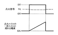
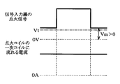
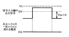
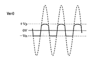
- the block diagram of the ignition device which shows 1st Embodiment of this indication Waveform diagram of ignition signal on signal input line and current flowing in primary coil of ignition coil Waveform diagram of ignition signal on signal input line and current flowing in primary coil of ignition coil Waveform diagram of ignition signal on signal input line and current flowing in primary coil of ignition coil Waveform diagram of clamped AC noise Waveform diagram of clamped AC noise Waveform diagram of clamped AC noise Waveform diagram of clamped AC noise
- the block diagram of the ignition device which shows 2nd Embodiment of this indication The block diagram of the ignition device which shows 3rd Embodiment of this indication
- the block diagram of the ignition device which shows 4th Embodiment of this indication The block diagram of the ignition device which shows 5th Embodiment of this indication
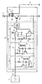
- An ignition device 1 (internal combustion engine ignition device) shown in FIG. 1 includes a control IC 2, an IGBT 3, and an ignition coil 4.
- the control IC 2 is a drive control circuit that outputs a drive signal (gate signal) for driving the IGBT 3 on and off in accordance with an ignition signal (input signal) sent from the engine ECU 5 via the wire line W.
- the IGBT 3 is a switching element that performs energization and interruption of the current flowing through the ignition coil 4 (load), and is provided separately from the control IC 2. Between the power supply line 6 to which the battery voltage + B is supplied and the ground line 7, the primary coil 4p of the ignition coil 4 and the collector and emitter of the IGBT 3 are connected in series. The secondary coil 4 s of the ignition coil 4 is connected to the plug 8. A diode 9 is connected between the coil ends of the primary coil 4p and the secondary coil 4s.
- the control IC 2 inputs an ignition signal from the input terminal Tin and outputs a drive signal from the output terminal Tout.
- the control IC 2 is a power supply circuit (not shown) that generates a control power supply voltage Vcc (for example, 5 V) from the battery voltage + B, and a positive noise protection connected between the signal input line 10 for the ignition signal and the ground line 7.
- Vcc control power supply voltage
- a circuit 11, a negative noise protection circuit 12, and a drive signal generation circuit 13 are provided.
- the positive noise protection circuit 11 is a first protection circuit that clamps the voltage of AC noise superimposed on the signal input line 10 at a level of + Vp (+ Vp> 0). Between the signal input line 10 and the ground line 7, the collector and emitter (between energization terminals) of the transistor 15 are connected. A resistor 14 is connected between the signal input line 10 and the collector of the transistor 15. A capacitor 16 (capacitive element) is connected between the signal input line 10 and the base (control terminal) of the transistor 15, and a resistor 17 (resistive element) is connected between the base of the transistor 15 and the ground line 7. ) Is connected. Zener diodes 18 and 19 connected in series so as to have opposite polarities are connected in parallel to the capacitor 16. In the signal input line 10, a resistor 20 is provided between a connection node of the resistor 14 and a connection node of the capacitor 16 and the Zener diode 18.
- the negative noise protection circuit 12 is a second protection circuit that clamps the voltage of AC noise superimposed on the signal input line 10 at a level of ⁇ Vn ( ⁇ Vn ⁇ 0).
- the negative noise protection circuit 12 includes diodes 21 to 23 connected in series between the signal input line 10 and the ground line 7 with the signal input line 10 side as a cathode. The number of diodes connected in series can be changed as appropriate.
- the drive signal generation circuit 13 generates a drive signal based on the comparison between the voltage Vs of the signal input line 10 and the threshold voltage Vt.
- the signal voltage Vs of the signal input line 10 is input to the non-inverting input terminal of the comparator 24 via the resistor 25, and the threshold voltage Vt is input from the threshold setting circuit 26 to the inverting input terminal.
- the threshold setting circuit 26 includes resistors 27 and 28 for dividing the power supply voltage Vcc, and a resistor 29 and a transistor 30 connected in series between the voltage dividing node and the ground line 7.
- the transistor 30 When the signal voltage Vs becomes lower than the threshold voltage Vt, the transistor 30 is turned off, so that the divided voltage by the resistors 27 and 28 becomes the threshold voltage Vt. When the signal voltage Vs becomes higher than the threshold voltage Vt, the transistor 30 is turned on, and the divided voltage by the resistors 27, 28, and 29 becomes the threshold voltage Vt. That is, the comparator 24 has a hysteresis characteristic.
- the drive circuit 31 amplifies the output signal of the comparator 24 and outputs a drive signal (gate signal).
- a positive polarity and a negative polarity are established between the signal input line 10 and the ground line 7 when a surge is applied. If necessary, a surge protection circuit is provided.
- the ignition signal output from the engine ECU 5 to the wire line W has a binary level voltage waveform, for example, the L level voltage VL is 0V and the H level voltage VH is 5V. If there is no influence of AC noise and a surge intrusion described later, when the ignition signal becomes H level, the signal voltage Vs of the signal input line 10 becomes higher than the threshold voltage Vt, and the IGBT 3 is turned on. Thereby, the current of the primary coil 4p of the ignition coil 4 increases.
- the ignition signal becomes L level
- the signal voltage Vs becomes lower than the threshold voltage Vt
- the IGBT 3 is turned off.
- the energy accumulated in the primary coil 4p is transferred to the secondary coil 4s, and ignition is performed by the plug 8.
- AC noise is likely to be induced in the wire line W arranged in the vehicle.
- the AC noise has a frequency of about 1 MHz to 500 MHz, for example.
- This AC noise also enters the control IC 2 of the ignition device 1 through the signal input line 10.
- the positive noise protection circuit 11 when the voltage Vs of the signal input line 10 rises due to AC noise, a current flows to the resistor 17 through the capacitor 16, and the transistor 15 is turned on by the voltage drop of the resistor 17. As a result, the positive noise protection circuit 11 clamps AC noise at a level of approximately + Vp (+ Vp> 0).
- the negative noise protection circuit 12 clamps at the level of ⁇ Vn ( ⁇ Vn ⁇ 0).
- Vn 3Vf (Vf: forward voltage of the diode).
- Vf forward voltage of the diode
- the comparator 24 compares the shifted signal voltage Vs with the threshold voltage Vt. As a result, when the average voltage Vm is equal to or higher than the threshold voltage Vt, the IGBT 3 is turned on even if the ignition signal is at the L level. Conversely, when the average voltage Vm is equal to or lower than (threshold voltage Vt ⁇ 5V), the IGBT 3 is turned off even if the ignition signal is at the H level.
- the clamp characteristic (clamp level: + Vp) of the positive noise protection circuit 11 is determined so that the H level of the ignition signal superimposed with the AC noise is higher than the threshold voltage Vt.
- the clamp characteristic (clamp level: ⁇ Vn) of the negative noise protection circuit 12 is determined so that the L level of the ignition signal on which AC noise is superimposed is lower than the threshold voltage Vt.
- the clamp level + Vp of the positive noise protection circuit 11 is set by adjusting the base current of the transistor 15 and thus the collector current.
- the adjustment factor for this is the impedance of the capacitor 16 and the resistors 17 and 20 at the frequency of the AC noise.
- the clamp level ⁇ Vn of the negative noise protection circuit 12 is set by adjusting the number of diodes connected in series.
- the average voltage Vm can be brought close to zero by adjusting at least one of the clamp levels + Vp and ⁇ Vn.
- the positive noise protection circuit 11 temporarily turns on the transistor 15.
- the circuit constant of the positive noise protection circuit 11 is set according to the frequency band of AC noise. The repetition frequency of the ignition signal is much lower than the frequency of AC noise. For this reason, after the ignition signal rises to the H level, the transistor 15 is turned off and the clamping action does not occur on the ignition signal.
- the ignition device 1 of the present embodiment includes the positive noise protection circuit 11 and the negative noise protection circuit 12, and clamps both the positive voltage and negative voltage of AC noise superimposed on the signal input line 10.
- the positive / negative asymmetry of the clamped alternating current noise waveform is improved, the average voltage Vm of the clamped alternating current noise can be reduced.
- fluctuations in the voltage level of the ignition signal due to AC noise can be suppressed.
- the clamp level + Vp of the positive noise protection circuit 11 and the clamp level ⁇ Vn of the negative noise protection circuit 12 are set so as to satisfy the above-described expression (1).
- the drive signal generation circuit 13 can perform normal ignition drive without erroneously determining the level of the ignition signal.
- the average voltage Vm of the clamped AC noise becomes zero by setting the clamp levels + Vp and ⁇ Vn equal to each other. Even when the AC noise has positive and negative asymmetry, the average voltage Vm of AC noise can be brought close to zero by individually adjusting the magnitudes of the clamp levels + Vp and ⁇ Vn. As a result, the decrease in the margin of the L level voltage VL or the H level voltage VH with respect to the threshold voltage Vt can be made zero.
- the ignition device 1 of the present embodiment is superior in noise resistance than the conventional configuration, and can prevent malfunction even in a more severe noise environment.
- the capacitor 16 can be protected from a high-frequency surge due to ESD or the like. Since the Zener diodes 18 and 19 have a Zener capacitance, by complementing the frequency characteristics with the capacitor 16, the clamping action can be maintained against AC noise in a wider frequency band.
- a capacitance value of about several ⁇ F is required. Met.
- the capacitor 16 included in the positive noise protection circuit 11 has a capacitance value of several tens of pF, the positive noise protection circuit 11 can be built in the control IC 2. Thereby, the enlargement of the ignition device 1 and the complication of assembly work can be avoided.
- the ignition device 41 shown in FIG. 4 differs from the ignition device 1 shown in FIG. 1 only in the configuration of the positive noise protection circuit 43 of the control IC 42. That is, in the positive noise protection circuit 43, the resistor 44 and the capacitor 16 are connected in series between the collector and base of the transistor 15, and the resistor 20 is removed from the signal input line 10. Zener diodes 18 and 19 connected in series are connected to the capacitor 16 in parallel.
- the capacitor 16 is connected between the signal input line 10 and the base of the transistor 15 via the resistors 14 and 44.
- Other configurations of the positive noise protection circuit 43 are the same as those of the positive noise protection circuit 11.
- the resistors 14 and 44 serve as adjustment elements for the base current of the transistor 15 and thus the collector current. Also according to the present embodiment, the same operations and effects as those of the first embodiment can be obtained.
- the ignition device 51 shown in FIG. 5 differs from the ignition device 1 shown in FIG. 1 in the configurations of the positive noise protection circuit 53 and the negative noise protection circuit 54 of the control IC 52.
- a diode 55 having an anode on the signal input line 10 side and a Zener diode 56 having a cathode on the signal input line 10 side are connected in series between the signal input line 10 and the ground line 7. It has the structure which was made.
- a diode 57 having a cathode on the signal input line 10 side and a Zener diode 58 having an anode on the signal input line 10 side are connected in series between the signal input line 10 and the ground line 7. It has the structure which was made.
- the clamp level + Vp of the positive noise protection circuit 53 is a voltage obtained by adding the forward voltage Vf of the diode 55 to the Zener voltage of the Zener diode 56.
- the clamp level ⁇ Vn of the negative noise protection circuit 54 is also a voltage obtained by adding the forward voltage Vf of the diode 57 to the Zener voltage of the Zener diode 58.
- the average voltage Vm of the clamped AC noise can be made zero by setting the Zener voltages of the Zener diodes 56 and 58 equal. Also according to the present embodiment, the same operations and effects as those of the first embodiment can be obtained.
- An ignition device 61 shown in FIG. 6 includes a positive noise protection circuit 43 shown in FIG. 4 and a circuit identical to the positive noise protection circuit 43 in the control IC 62 in the opposite direction with respect to the signal input line 10 and the ground line 7. And a negative noise protection circuit 63 connected thereto.
- Other configurations are the same as those of the ignition device 1.
- the negative noise protection circuit 63 acts on the negative voltage of the AC noise in the same manner as the positive noise protection circuit 43.
- the same operation and effect as the first and second embodiments can be obtained. Further, if the same circuit constant is used in the positive noise protection circuit 43 and the negative noise protection circuit 63, the magnitudes of the clamp levels + Vp and -Vn become equal.
- the ignition device 71 shown in FIG. 7 differs from the ignition device 61 shown in FIG. 6 in the configurations of the positive noise protection circuit 73 and the negative noise protection circuit 74 of the control IC 72.
- the positive noise protection circuit 73 and the negative noise protection circuit 74 are obtained by replacing the resistor 14 of the positive noise protection circuit 43 and the negative noise protection circuit 63 with a diode 75, respectively.
- the voltage applied between the collector and emitter (or between the collector and base) of the transistor 15 changes according to the current.
- the diode 75 the voltage applied between the collector and emitter (or between the collector and base) of the transistor 15 is reduced by a constant voltage regardless of the magnitude of the current. For this reason, the prospects of adjusting the clamp levels + Vp and ⁇ Vn are improved, and the adjustment becomes easy.
- operations and effects similar to those of the first and second embodiments can be obtained.
- the circuit selected from the positive noise protection circuits 11, 43, 53, 73 and the circuit selected from the negative noise protection circuits 12, 54, 63, 74 may be arbitrarily combined.
- a capacitive element such as a series circuit of a capacitor and a resistor may be provided.
- a resistive element such as a series circuit of a resistor and a capacitor may be provided.
- the resistor 44 may be provided as necessary.
- the Zener diodes 18 and 19 may be provided as necessary.
- the average voltage Vm can be brought close to zero by adjusting at least one of the clamp levels + Vp and ⁇ Vn.
- the drive signal generation circuit 13 may have hysteresis characteristics as necessary.
- transistor 15 having an energization terminal (collector, emitter) and a control terminal (base)
- an FET having an energization terminal (drain, source) and a control terminal (gate) may be used.
- the IGBT 3 may be configured as a semiconductor chip or may be configured by a discrete element. Instead of configuring the IGBT 3 and the control ICs 2, 42, 52, 62, and 72 as separate semiconductor chips (multi-chip configuration), the IGBT 3 and the control ICs 2, 42, 52, 62, and 72 are combined into one semiconductor chip. It is good also as a structure (single-chip structure).
- the drive control circuit according to the present disclosure is not limited to an internal combustion engine ignition device, and can be widely applied to devices that generate a drive signal for a switching element according to an input signal.
Landscapes
- Engineering & Computer Science (AREA)
- Chemical & Material Sciences (AREA)
- Combustion & Propulsion (AREA)
- Mechanical Engineering (AREA)
- General Engineering & Computer Science (AREA)
- Ignition Installations For Internal Combustion Engines (AREA)
Abstract
Description
以下、本開示の第1の実施形態について図1から図3Cを参照しながら説明する。図1に示す点火装置1(内燃機関点火装置)は、制御IC2、IGBT3および点火コイル4を備えている。制御IC2は、エンジンECU5からワイヤラインWを介して送られてくる点火信号(入力信号)に従って、IGBT3をオンオフ駆動する駆動信号(ゲート信号)を出力する駆動制御回路である。
すなわち、正ノイズ保護回路11のクランプ特性(クランプレベル:+Vp)は、交流ノイズが重畳した点火信号のHレベルがしきい値電圧Vtより高くなるように決定されている。負ノイズ保護回路12のクランプ特性(クランプレベル:-Vn)は、交流ノイズが重畳した点火信号のLレベルがしきい値電圧Vtより低くなるように決定されている。
図4に示す点火装置41は、図1に示した点火装置1に対し、制御IC42の正ノイズ保護回路43の構成のみが相違する。すなわち、正ノイズ保護回路43において、トランジスタ15のコレクタ・ベース間に抵抗44とコンデンサ16とが直列に接続されており、信号入力線10から抵抗20が除かれている。コンデンサ16には、直列に接続されたツェナーダイオード18、19が並列に接続されている。
図5に示す点火装置51は、図1に示した点火装置1に対し、制御IC52の正ノイズ保護回路53および負ノイズ保護回路54の構成が相違する。正ノイズ保護回路53は、信号入力線10とグランド線7との間に、信号入力線10側をアノードとするダイオード55と、信号入力線10側をカソードとするツェナーダイオード56とが直列に接続された構成を備えている。負ノイズ保護回路54は、信号入力線10とグランド線7との間に、信号入力線10側をカソードとするダイオード57と、信号入力線10側をアノードとするツェナーダイオード58とが直列に接続された構成を備えている。
図6に示す点火装置61は、制御IC62内に、図4に示した正ノイズ保護回路43と、この正ノイズ保護回路43と同一の回路を信号入力線10とグランド線7に対し逆向きに接続した負ノイズ保護回路63とを備えている。その他の構成は点火装置1と同様である。当然のことながら、負ノイズ保護回路63は、交流ノイズの負電圧に対して正ノイズ保護回路43と同様に作用する。本実施形態によっても、第1、第2の実施形態と同様の作用および効果が得られる。また、正ノイズ保護回路43と負ノイズ保護回路63とで同じ回路定数を用いれば、クランプレベル+Vpと-Vnの大きさが等しくなる。
図7に示す点火装置71は、図6に示した点火装置61に対し、制御IC72の正ノイズ保護回路73および負ノイズ保護回路74の構成が相違する。正ノイズ保護回路73、負ノイズ保護回路74は、それぞれ正ノイズ保護回路43、負ノイズ保護回路63の抵抗14をダイオード75で置き替えたものである。
以上、本開示の好適な実施形態について説明したが、本開示は上述した実施形態に限定されるものではなく、開示の要旨を逸脱しない範囲内で種々の変形、拡張を行うことができる。
Claims (12)
- 入力信号に従って、負荷(4)に流れる電流を通断電するスイッチング素子(3)の駆動信号を生成する駆動制御回路(2,42,52,62,72)であって、
前記入力信号の信号入力線(10)とグランド線(7)との間に接続され、前記信号入力線に重畳する交流ノイズの電圧を+Vp(+Vp>0)のレベルでクランプする第1の保護回路(11,43,53,73)と、
前記信号入力線と前記グランド線との間に接続され、前記信号入力線に重畳する交流ノイズの電圧を-Vn(-Vn<0)のレベルでクランプする第2の保護回路(12,54,63,74)と、
前記信号入力線の電圧としきい値電圧Vtとの比較に基づいて前記駆動信号を生成する駆動信号生成回路(13)とを備え、
前記入力信号がLレベル電圧VLとHレベル電圧VHの2値レベルを持ち、前記クランプレベル+Vpと-Vnとでクランプされた交流ノイズの平均電圧が、前記しきい値電圧Vtと前記Lレベル電圧VLとの差電圧(Vt-VL)よりも低く、且つ、前記しきい値電圧Vtと前記Hレベル電圧VHとの差電圧(Vt-VH)よりも高くなるように、前記クランプレベル+Vpと-Vnが設定されている駆動制御回路。 - 前記第1の保護回路(11,43,73)は、
前記信号入力線と前記グランド線との間に通電端子間が接続され、前記グランド線に接続された通電端子と制御端子との間に与えられる制御電圧に応じてオンオフ動作するトランジスタ(15)と、
前記信号入力線と前記トランジスタの制御端子との間に接続された容量性素子(16)と、
前記トランジスタの制御端子と前記グランド線との間に接続された抵抗性素子(17)とを備えて構成されている請求項1記載の駆動制御回路。 - 前記信号入力線と前記容量性素子との間に抵抗(14,44)が介在している請求項2記載の駆動制御回路。
- 前記信号入力線と前記容量性素子との間に、前記信号入力線側をアノードとするダイオード(75)が介在している請求項2記載の駆動制御回路。
- 前記第1の保護回路(53)は、前記信号入力線と前記グランド線との間に、前記信号入力線側をアノードとするダイオード(55)と、前記信号入力線側をカソードとするツェナーダイオード(56)とが直列に接続されて構成されている請求項1記載の駆動制御回路。
- 前記第2の保護回路(12)は、前記信号入力線と前記グランド線との間に、前記信号入力線側をカソードとして接続された1または複数直列のダイオード(21~23)を備えて構成されている請求項1から5の何れか一項に記載の駆動制御回路。
- 前記第2の保護回路(63)は、
前記信号入力線と前記グランド線との間に通電端子間が接続され、前記信号入力線に接続された通電端子と制御端子との間に与えられる制御電圧に応じてオンオフ動作するトランジスタ(15)と、
前記トランジスタの制御端子と前記グランド線との間に接続された容量性素子(16)と、
前記信号入力線と前記トランジスタの制御端子との間に接続された抵抗性素子(17)とを備えて構成されている請求項1から5の何れか一項に記載の駆動制御回路。 - 前記容量性素子と前記グランド線との間に抵抗(14,44)が介在している請求項7記載の駆動制御回路。
- 前記容量性素子と前記グランド線との間に、前記グランド線側をアノードとするダイオード(75)が介在している請求項7記載の駆動制御回路。
- 前記第2の保護回路(54)は、前記信号入力線と前記グランド線との間に、前記信号入力線側をカソードとするダイオード(57)と、前記信号入力線側をアノードとするツェナーダイオード(58)とが直列に接続されて構成されている請求項1から5の何れか一項に記載の駆動制御回路。
- 前記容量性素子に、互いに逆極性となるように直列に接続されたツェナーダイオード(18,19)が並列に接続されている請求項2、3、4、7、8、9の何れか一項に記載の駆動制御回路。
- 点火コイル(4)に流れる電流の通断電を行うスイッチング素子(3)と、
前記スイッチング素子の駆動信号を生成する請求項1から11の何れか一項に記載の駆動制御回路(2,42,52,62,72)とを備えている内燃機関点火装置。
Priority Applications (2)
| Application Number | Priority Date | Filing Date | Title |
|---|---|---|---|
| US14/781,098 US9920735B2 (en) | 2013-04-16 | 2014-04-15 | Drive control circuit, and ignition device for internal combustion engine |
| CN201480021364.6A CN105143662B (zh) | 2013-04-16 | 2014-04-15 | 驱动控制电路以及内燃机点火装置 |
Applications Claiming Priority (2)
| Application Number | Priority Date | Filing Date | Title |
|---|---|---|---|
| JP2013-085720 | 2013-04-16 | ||
| JP2013085720A JP5929817B2 (ja) | 2013-04-16 | 2013-04-16 | 駆動制御回路および内燃機関点火装置 |
Publications (1)
| Publication Number | Publication Date |
|---|---|
| WO2014171127A1 true WO2014171127A1 (ja) | 2014-10-23 |
Family
ID=51731090
Family Applications (1)
| Application Number | Title | Priority Date | Filing Date |
|---|---|---|---|
| PCT/JP2014/002113 Ceased WO2014171127A1 (ja) | 2013-04-16 | 2014-04-15 | 駆動制御回路および内燃機関点火装置 |
Country Status (4)
| Country | Link |
|---|---|
| US (1) | US9920735B2 (ja) |
| JP (1) | JP5929817B2 (ja) |
| CN (1) | CN105143662B (ja) |
| WO (1) | WO2014171127A1 (ja) |
Families Citing this family (3)
| Publication number | Priority date | Publication date | Assignee | Title |
|---|---|---|---|---|
| JP7143398B2 (ja) * | 2018-03-13 | 2022-09-28 | ローム株式会社 | スイッチ制御回路、イグナイタ |
| JP7293736B2 (ja) * | 2019-03-07 | 2023-06-20 | 富士電機株式会社 | 半導体集積回路 |
| JP7676933B2 (ja) * | 2021-05-17 | 2025-05-15 | 富士電機株式会社 | 集積回路 |
Citations (4)
| Publication number | Priority date | Publication date | Assignee | Title |
|---|---|---|---|---|
| JPH0310631U (ja) * | 1989-06-15 | 1991-01-31 | ||
| JPH0522099A (ja) * | 1991-07-11 | 1993-01-29 | Nissan Motor Co Ltd | 半導体入力保護回路 |
| JP2006046255A (ja) * | 2004-08-06 | 2006-02-16 | Denso Corp | 内燃機関用点火装置 |
| JP2007303317A (ja) * | 2006-05-10 | 2007-11-22 | Diamond Electric Mfg Co Ltd | 内燃機関の失火検出装置 |
Family Cites Families (10)
| Publication number | Priority date | Publication date | Assignee | Title |
|---|---|---|---|---|
| GB1562319A (en) * | 1975-11-26 | 1980-03-12 | Beckman Instruments Inc | Ignition analyzer for use with electronic ignition systems |
| JPS5440941A (en) | 1977-09-07 | 1979-03-31 | Automob Antipollut & Saf Res Center | Ignition apparatus for internal combustion engine |
| US5636097A (en) * | 1991-05-09 | 1997-06-03 | Consorzio Per La Ricerca Sulla Microelettronica | Protective circuit for semiconductor power device |
| JP3505197B2 (ja) * | 1993-04-12 | 2004-03-08 | 三菱電機株式会社 | 波形整形回路 |
| JP3110242B2 (ja) * | 1994-03-24 | 2000-11-20 | 三菱電機株式会社 | 点火検出装置 |
| JP4360299B2 (ja) * | 2004-08-06 | 2009-11-11 | 株式会社デンソー | 内燃機関用点火装置 |
| JP4455972B2 (ja) * | 2004-10-08 | 2010-04-21 | 三菱電機株式会社 | 半導体装置 |
| JP4924705B2 (ja) * | 2009-04-15 | 2012-04-25 | 株式会社デンソー | 内燃機関点火装置 |
| CN105144580B (zh) * | 2013-04-02 | 2017-12-19 | 三菱电机株式会社 | 半导体装置 |
| JP6672816B2 (ja) * | 2016-01-15 | 2020-03-25 | 富士電機株式会社 | スイッチ装置 |
-
2013
- 2013-04-16 JP JP2013085720A patent/JP5929817B2/ja not_active Expired - Fee Related
-
2014
- 2014-04-15 WO PCT/JP2014/002113 patent/WO2014171127A1/ja not_active Ceased
- 2014-04-15 US US14/781,098 patent/US9920735B2/en not_active Expired - Fee Related
- 2014-04-15 CN CN201480021364.6A patent/CN105143662B/zh not_active Expired - Fee Related
Patent Citations (4)
| Publication number | Priority date | Publication date | Assignee | Title |
|---|---|---|---|---|
| JPH0310631U (ja) * | 1989-06-15 | 1991-01-31 | ||
| JPH0522099A (ja) * | 1991-07-11 | 1993-01-29 | Nissan Motor Co Ltd | 半導体入力保護回路 |
| JP2006046255A (ja) * | 2004-08-06 | 2006-02-16 | Denso Corp | 内燃機関用点火装置 |
| JP2007303317A (ja) * | 2006-05-10 | 2007-11-22 | Diamond Electric Mfg Co Ltd | 内燃機関の失火検出装置 |
Also Published As
| Publication number | Publication date |
|---|---|
| US9920735B2 (en) | 2018-03-20 |
| US20160061178A1 (en) | 2016-03-03 |
| JP2014208975A (ja) | 2014-11-06 |
| JP5929817B2 (ja) | 2016-06-08 |
| CN105143662A (zh) | 2015-12-09 |
| CN105143662B (zh) | 2017-05-24 |
Similar Documents
| Publication | Publication Date | Title |
|---|---|---|
| US10236677B2 (en) | Semiconductor device | |
| JP2020036530A (ja) | スイッチング素子の駆動制御装置 | |
| TWI571031B (zh) | 保護裝置、系統及維持閘極驅動器端子上的穩定輸出的方法 | |
| US9350142B2 (en) | Signal detection circuit, igniter, and vehicle using the same | |
| WO2014097486A1 (ja) | スイッチング素子駆動回路、パワーモジュールおよび自動車 | |
| US10122191B2 (en) | Battery protection circuit | |
| JP7271933B2 (ja) | 絶縁ゲート型デバイス駆動装置 | |
| JP4961977B2 (ja) | 過電流保護回路 | |
| US8901967B2 (en) | Comparator | |
| JP5929817B2 (ja) | 駆動制御回路および内燃機関点火装置 | |
| TWI595628B (zh) | 靜電放電防護電路及積體電路 | |
| CN102057573B (zh) | 负载电路的过电流保护装置 | |
| CN110166031B (zh) | 半导体装置 | |
| JP2016092534A (ja) | イグナイタおよび車両、イグニッションコイルの制御方法 | |
| JP2015092790A (ja) | 半導体スイッチング素子の保護回路および電力変換装置 | |
| AU2010244995B2 (en) | Method and apparatus for protecting transistors | |
| CN205377651U (zh) | 一种耐浪涌保护电路 | |
| JP2016131465A (ja) | ゲート駆動回路 | |
| CN109991466A (zh) | 检测装置,保护系统及保护方法 | |
| CN103973236B (zh) | 输入保护电路 | |
| JP7676933B2 (ja) | 集積回路 | |
| JP6712537B2 (ja) | 差動増幅器 | |
| CN107528310B (zh) | 具有负载突降保护的电子装置 | |
| WO2015060095A1 (ja) | センサ装置 | |
| CN105429124A (zh) | 用于高压集成电路的输入过压保护电路 |
Legal Events
| Date | Code | Title | Description |
|---|---|---|---|
| WWE | Wipo information: entry into national phase |
Ref document number: 201480021364.6 Country of ref document: CN |
|
| 121 | Ep: the epo has been informed by wipo that ep was designated in this application |
Ref document number: 14786068 Country of ref document: EP Kind code of ref document: A1 |
|
| WWE | Wipo information: entry into national phase |
Ref document number: 14781098 Country of ref document: US |
|
| NENP | Non-entry into the national phase |
Ref country code: DE |
|
| 122 | Ep: pct application non-entry in european phase |
Ref document number: 14786068 Country of ref document: EP Kind code of ref document: A1 |