WO2014170969A1 - 基板処理システム - Google Patents
基板処理システム Download PDFInfo
- Publication number
- WO2014170969A1 WO2014170969A1 PCT/JP2013/061355 JP2013061355W WO2014170969A1 WO 2014170969 A1 WO2014170969 A1 WO 2014170969A1 JP 2013061355 W JP2013061355 W JP 2013061355W WO 2014170969 A1 WO2014170969 A1 WO 2014170969A1
- Authority
- WO
- WIPO (PCT)
- Prior art keywords
- substrate
- carrier
- substrate carrier
- processing
- processing system
- Prior art date
- Legal status (The legal status is an assumption and is not a legal conclusion. Google has not performed a legal analysis and makes no representation as to the accuracy of the status listed.)
- Ceased
Links
Images





Classifications
-
- H—ELECTRICITY
- H10—SEMICONDUCTOR DEVICES; ELECTRIC SOLID-STATE DEVICES NOT OTHERWISE PROVIDED FOR
- H10P—GENERIC PROCESSES OR APPARATUS FOR THE MANUFACTURE OR TREATMENT OF DEVICES COVERED BY CLASS H10
- H10P72/00—Handling or holding of wafers, substrates or devices during manufacture or treatment thereof
- H10P72/06—Apparatus for monitoring, sorting, marking, testing or measuring
- H10P72/0606—Position monitoring, e.g. misposition detection or presence detection
Definitions
- the present invention relates to a substrate processing system in which a substrate to be processed is mounted on a substrate carrier and stored in a processing apparatus.
- a substrate to be processed is mounted on a substrate carrier and carried into a processing apparatus in processing steps such as film formation and etching in manufacturing a semiconductor device such as a solar battery cell.
- a substrate processing system using a substrate carrier the substrate carrier on which the substrate is mounted is transported between the transfer device and the processing device (see, for example, Patent Document 1).
- the substrate is moved between the substrate tray storing the substrate and the substrate carrier by the transfer device. That is, the unprocessed substrate taken out from the substrate tray by the transfer device is mounted on the substrate carrier. After the processing step, the processed substrate is recovered from the substrate carrier by the transfer device and stored in the substrate tray.
- substrate transfer the mounting of the substrate on the substrate carrier and the recovery of the substrate from the substrate carrier are collectively referred to as “substrate transfer”.
- the entire substrate processing system is automated in response to a request to increase the processing capacity (throughput). For this reason, in transferring the substrate on the substrate carrier, the substrate is transferred between the substrate tray and the substrate carrier, for example, using a robot arm.
- the substrate when the substrate is transferred by the substrate carrier, the substrate may not be mounted at a normal position or the substrate may not be mounted in a normal posture.
- the substrate carrier When the substrate carrier is carried into the processing apparatus in such a state, there may be a problem that the processing apparatus fails.
- the substrate may be detached from the substrate carrier or the posture of the substrate may be disturbed during the processing process in the processing apparatus.
- the substrate carrier is carried into the transfer device in such a state and a transfer operation is performed, problems such as failure of the transfer device may occur.
- the substrate may be damaged due to the substrate falling from the substrate carrier or due to the substrate not being mounted in a normal position, the substrate contacting a component in the processing apparatus, or the like.
- an object of the present invention is to provide a substrate processing system capable of suppressing failures caused by a substrate not being normally mounted on a substrate carrier.
- a transfer device for transferring a substrate to a substrate carrier, (b) a processing device for processing a substrate mounted on the substrate carrier, and (c) a transfer device. And a transfer device for transferring the substrate carrier between the processing device and (d) a substrate processing sensor for detecting whether or not the substrate is normally mounted on the substrate carrier between the transfer device and the processing device.
- the present invention it is possible to provide a substrate processing system capable of suppressing failures caused by the substrate not being normally mounted on the substrate carrier.
- the substrate 100 to be processed is mounted on the substrate carrier 10 and carried into the processing apparatus 30.
- the substrate processing system 1 includes a transfer device 20 for transferring the substrate 100 to the substrate carrier 10, a processing device 30 for processing the substrate 100 mounted on the substrate carrier 10, and the transfer device 20 and the processing device 30. And a substrate mounting sensor 50 that detects whether or not the substrate 100 is normally mounted on the substrate carrier 10 between the transfer device 20 and the processing device 30.
- the substrate carrier 10 on which the substrate 100 is mounted circulates between the transfer device 20 and the processing device 30 by the transport device 40.
- an arrow attached to the substrate carrier 10 on the transfer device 40 indicates the transfer direction of the substrate carrier 10.
- the transport apparatus 40 includes a first transport path 41 that transports the substrate carrier 10 from the transfer apparatus 20 to the processing apparatus 30, and a second transport path 42 that transports the substrate carrier 10 from the processing apparatus 30 to the transfer apparatus 20. Is provided.
- the several substrate carrier 10 may be conveyed simultaneously by the conveying apparatus 40, and the substrate carrier 10 used in the substrate processing system 1 may be one.
- the substrate mounting sensor 50 has a position where the substrate carrier 10 is unloaded from the transfer device 20 in the first transfer path 41 and the transfer device 20 in the second transfer path 42. Are arranged at positions where the substrate carrier 10 is loaded.
- the substrate mounting sensor 50 disposed on the first transport path 41 is referred to as a “carrying-out side substrate mounting sensor 51”, and the substrate mounting sensor 50 disposed on the second transport path 42. Is referred to as a “load-in side substrate mounting sensor 52”.
- the substrate carrier 10 includes a cart type in which the substrate 100 is mounted horizontally and a boat type in which the substrate 100 is mounted vertically.
- the boat-type substrate carrier 10 includes a cart type in which the substrate 100 is mounted horizontally and a boat type in which the substrate 100 is mounted vertically.
- it is effective to increase the number of substrates 100 that can be processed simultaneously using the boat-type substrate carrier 10. That is, by using a boat-type substrate carrier 10 having a plurality of substrate plates 11 on which the substrates 100 are mounted as shown in FIG. 2, the footprint of the processing apparatus 30 that simultaneously processes a large number of substrates 100 is reduced. be able to.
- a plurality of substrate plates 11 each having a bottom portion fixed to one bottom plate 12 are usually arranged along the surface normal direction of the substrate mounting surface 110.
- a case where the substrate carrier 10 is a boat type will be described as an example.
- a substrate mounting area 111 on which the substrate 100 is mounted is defined by being arranged in the horizontal direction.
- One substrate 100 is mounted on one substrate mounting area 111.
- the number of substrates 100 mounted on one substrate mounting surface 110 can be arbitrarily set.
- the number of substrate mounting areas 111 defined on one substrate mounting surface 110 may be one.
- two opposing main surfaces of the substrate plate 11 may be used as the substrate mounting surface 110, respectively.
- the substrate 100 is supported on the substrate mounting region 111 by a fixing pin (not shown) disposed on the substrate mounting surface 110.
- the substrate 100 is a substrate used for a semiconductor device or a solar battery cell such as a silicon substrate or a glass substrate.
- the transfer apparatus 20 collects the processed substrate 100 processed by the processing apparatus 30 from the substrate carrier 10 and mounts the unprocessed substrate 100 to be processed by the processing apparatus 30 on the substrate carrier 10.
- the substrate tray 200 in which the unprocessed substrate 100 is stored is carried into the transfer device 20. Then, the substrate 100 is transferred from the substrate tray 200 to the substrate carrier 10. Further, the processed substrate 100 is collected from the substrate carrier 10 and stored in the substrate tray 200. As described above, the transfer apparatus 20 exchanges the processed substrate 100 and the unprocessed substrate 100 in the substrate carrier 10.
- the transfer operation of the substrate 100 in the transfer apparatus 20 is performed by, for example, a robot arm 21 as shown in FIG. That is, at the time of substrate recovery, the substrate 100 mounted on the substrate carrier 10 is held by the robot arm 21 by vacuum suction or the like. Thereafter, the robot arm 21 is moved to recover the substrate 100 from the substrate carrier 10, and the substrate 100 is stored in the substrate tray 200. Further, when the substrate is mounted, the substrate 100 is taken out from the substrate tray 200 by the robot arm 21. Then, after placing the substrate 100 on the substrate carrier 10, the robot arm 21 releases the substrate 100, and the substrate 100 is mounted on the substrate carrier 10. As shown in FIG. 4, the transfer apparatus 20 can simultaneously mount a plurality of substrates 100 on the substrate mounting surface 110.
- the processing apparatus 30 is, for example, an in-line manufacturing apparatus including a substrate taking-in chamber 31, a processing chamber 32, and a substrate taking-out chamber 33 as shown in FIG.
- a film forming process, an etching process, a sputtering process, and the like are performed in the processing chamber 32.
- the substrate carrier 10 on which the substrate 100 is mounted is taken into the substrate take-in chamber 31. Then, the substrate carrier 10 is transferred from the substrate take-in chamber 31 to the processing chamber 32, and predetermined processing is performed in the processing chamber 32. For example, after a thin film is formed on the substrate 100 in the processing chamber 32, the substrate carrier 10 is transferred from the processing chamber 32 to the substrate extraction chamber 33. Thereafter, the substrate carrier 10 is taken out from the substrate take-out chamber 33.
- the processing apparatus 30 may have a structure including the substrate take-in chamber 31 and the process chamber 32 without the substrate take-out chamber 33.
- the substrate carrier 10 is used as an anode electrode. After introducing the source gas into the processing chamber 32, electric power is supplied between the substrate carrier 10 and the cathode electrode to bring the source gas into a plasma state. By exposing the substrate 100 to the formed plasma, a desired thin film mainly composed of the raw material contained in the raw material gas is formed on the exposed surface of the substrate 100. By appropriately selecting the source gas, a desired thin film such as a silicon semiconductor thin film, a silicon nitride thin film, a silicon oxide thin film, a silicon oxynitride thin film, or a carbon thin film can be formed on the substrate 100.
- a desired thin film such as a silicon semiconductor thin film, a silicon nitride thin film, a silicon oxide thin film, a silicon oxynitride thin film, or a carbon thin film can be formed on the substrate 100.
- a silicon nitride (SiN) film as an antireflection film or an insulating film is formed on the substrate 100 using a mixed gas of ammonia (NH 3 ) gas and silane (SiH 4 ) gas. Can be formed.
- NH 3 ammonia
- SiH 4 silane
- a film is formed on the substrate 100 in a state where the temperature of the substrate 100 to be processed is set to a predetermined temperature. For this reason, when the film forming process is performed by the processing apparatus 30, the substrate 100 is preheated in the substrate taking-in chamber 31 before being carried into the processing chamber 32. That is, the substrate taking-in chamber 31 also serves as a preheating chamber. Then, the substrate 100 that has reached the set temperature is carried into the processing chamber 32 and a film forming process is performed.
- the substrate mounting sensor 50 detects that the substrate 100 is mounted in a normal posture on the substrate carrier 10 and that the substrate 100 is mounted at a normal position of the substrate carrier 10.
- the substrate mounting sensor 50 is based on an image acquisition device 501 that captures a substrate mounting surface 110 of the substrate plate 11 on which the substrate 100 is mounted and acquires a determination image, and the determination image. And a determination device 502 that determines whether or not the substrate 100 is normally mounted on the substrate mounting surface 110.
- the image acquisition device 501 captures an image including the substrate mounting area 111 on the substrate mounting surface 110 when the substrate carrier 10 on which the substrate 100 is mounted moves on the transport device 40 and enters the imaging range. Thereby, an image that can determine the position and orientation of the position substrate 100 with respect to the substrate mounting region 111 is taken.
- the determination device 502 performs image processing on the image captured by the image acquisition device 501 to determine the position and orientation of the substrate 100. When the substrate 100 is not disposed at the set position of the substrate mounting area 111, the determination device 502 determines that the substrate 100 is not normally mounted on the substrate mounting surface 110.
- the determination device 502 determines that the substrate 100 is not normally mounted on the substrate carrier 10 when the image of the substrate 100 does not exist at a predetermined position of the determination image, for example.
- a CCD (Charge Coupled Device) camera or a CMOS (Complementary Metal Oxide Semiconductor) camera can be used as the image acquisition device 501.
- FIG. 6 shows an example in which the substrate mounting sensor 50 includes two image acquisition devices 501 and images two substrate mounting surfaces 110 facing each other on the substrate plate 11 at the same time. Thereby, mounting of the substrate 100 can be detected simultaneously on both surfaces of the substrate plate 11. On the other hand, when only one main surface of the substrate plate 11 is the substrate mounting surface 110, the mounting of the substrate 100 is detected on the substrate mounting surface 110 by one image acquisition device 501.
- the substrate mounting sensor 50 may determine whether or not the substrate 100 is normally mounted on the substrate mounting surface 110 by using means other than the imaging device.
- a detection device such as a reflective optical sensor can also be used for the substrate mounting sensor 50.
- the substrate carrier 10 When the substrate mounting sensor 50 detects that the substrate 100 is not normally mounted on the substrate carrier 10, for example, the substrate carrier 10 is taken out from the transfer device 40 and the substrate 100 is transferred again.
- the substrate carrier 10 detected by the carry-out substrate mounting sensor 51 that the substrate 100 is not normally mounted is transferred from the transfer device 40 via the first correction transfer path 61. It is taken out.
- the substrate carrier 10 detected by the carry-in substrate mounting sensor 52 that the substrate 100 is not normally mounted is taken out from the transport apparatus 40 via the second correction transport path 62.
- the transfer of the substrate 100 is performed again by an operator, for example.
- the substrate processing system 1 it is possible to prevent the substrate carrier 10 on which the substrate 100 is not normally mounted from being carried into the transfer device 20 or the processing device 30.
- FIG. 7 shows an example in which the substrate 100a is mounted on the substrate mounting surface 110 in a normal posture and the substrates 100b and 100c are not mounted on the substrate mounting surface 110 in a normal posture.
- FIG. 8 shows an example of the substrate 100e that is not in close contact with the substrate mounting surface 110 and the substrate 100f that is detached from the substrate mounting surface 110 with respect to the substrate 100d that is mounted at a normal position on the substrate mounting surface 110. Show.
- the substrate 100 When the substrate 100 is not normally mounted on the substrate carrier 10, for example, when the substrate 100 falls from the substrate carrier 10 in the processing apparatus 30, the substrate 100 is damaged or the transport mechanism in the processing apparatus 30 is It can be destroyed. Further, when the processing apparatus 30 is a film forming apparatus in which a film forming gas is injected from below, the gas outlet is blocked by the dropped substrate 100 or the gas flow is disturbed. Depending on the situation, normal processing may not be performed. Furthermore, normal processing may not be performed if the distance between the substrate 100 and the adjacent substrate plate 11 deviates from the set value.
- the substrate 100 is normally mounted on the substrate carrier 10 before the unload-side substrate mounting sensor 51 is unloaded from the transfer device 20 and loaded into the processing device 30. Is detected. Thereby, the failure
- the carry-out side substrate mounting sensor 51 is disposed at a position where the substrate mounting surface 110 of the substrate carrier 10 transported on the first transport path 41 can be photographed.
- the substrate carrier 10 is arranged around the first conveyance path 41 while the substrate carrier 10 is being conveyed from the transfer apparatus 10 to the processing apparatus 30. Since the carry-out side substrate mounting sensor 51 is not disposed in the processing apparatus 30, it is not necessary to consider that the surroundings are in a vacuum state. In addition, since the substrate carrier 10 moves along the first conveyance path 41, the substrate mounting surface 110 of the substrate carrier 10 can be sequentially photographed even if the position of the substrate mounting sensor 50 is fixed.
- the substrate carrier 10 is used for the film forming process in a state where the substrate 100 is not mounted in the substrate mounting region 111 or in a state where the substrate 100 is not mounted normally and a part of the substrate mounting region 111 is exposed. As a result, a film is formed in the substrate mounting region 111.
- the substrate 100 is supported by fixing pins arranged on the substrate mounting surface 110, but a portion of the fixed pins exposed on the substrate mounting region 111 is formed by cumulatively forming a film on the substrate mounting region 111. The length of is shortened. For this reason, the substrate 100 cannot be supported by the fixing pins, and the substrate 100 cannot be mounted on the substrate carrier 10.
- the surface of the substrate carrier 10 is insulated by the film in a plasma film forming apparatus using the substrate carrier 10 as an electrode. Electrical connection is degraded. This causes the substrate 100 to be in an electrically floating state, causing problems such as a decrease in film formation rate and a decrease in film thickness uniformity.
- the substrate mounting sensor 50 detects that the substrate is mounted on all the substrate mounting regions 111 defined in the substrate carrier 10, it is possible to prevent a film from being formed in the substrate mounting region 111.
- the substrate mounting sensor 50 detects that the substrates are mounted on all the substrate mounting areas 111 of the substrate carrier 10, for example, at the timing when each of the substrate mounting areas 111 enters the imaging range of the image acquisition device 501, Images are taken one by one for the region 111.
- a wide-angle lens may be used for the image acquisition device 501 to photograph all the board mounting areas 111 at the same time.
- the substrate 100 may be detached from the substrate carrier 10 or the posture of the substrate 100 on the substrate mounting surface 110 may be disturbed.
- the heated substrate 100 may be warped during processing in the processing apparatus 30, and the position of the substrate 100 may be displaced from the substrate mounting region 111 or the posture of the substrate 100 may be disturbed. If the substrate carrier 10 is carried into the transfer device 20 in this state and a transfer operation is performed, the substrate 100 may fall from the substrate carrier 10 and be damaged, or the robot arm 21 may hold the substrate 100 accurately. Can not.
- the robot arm 21 moves the substrate mounting area 111 where the substrate 100 is not mounted. May be adsorbed. As a result, the substrate carrier 10 is pulled by the robot arm 21 and the substrate carrier 10 is detached from the transfer device 40 or a failure such as the substrate 100 dropping from the substrate carrier 10 occurs.
- the substrate 100 is normally mounted on the substrate carrier 10 before the carry-in substrate mounting sensor 52 is unloaded from the processing apparatus 30 and loaded into the transfer apparatus 20. Is detected. Thereby, it is possible to prevent a failure of the transfer apparatus 20 and a stop of the automatic operation due to the substrate 100 not being normally mounted on the substrate carrier 10.
- the carry-in substrate mounting sensor 52 is disposed at a position where the substrate mounting surface 110 of the substrate carrier 10 transported on the second transport path 42 can be photographed.
- the substrate carrier 10 is arranged around the second conveyance path 42 while the substrate carrier 10 is being conveyed from the processing apparatus 30 to the transfer apparatus 10.
- the carry-in side substrate mounting sensor 52 is not arranged in the processing apparatus 30, and therefore it is not necessary to consider that the surroundings are in a vacuum state. Further, since the substrate carrier 10 moves along the second conveyance path 42, the substrate mounting surface 110 of the substrate carrier 10 can be sequentially photographed even if the position of the image acquisition device 501 is fixed.
- the substrate 100 is normally placed on the substrate carrier 10 immediately after being unloaded from the transfer device 20 or just before being loaded into the transfer device 20. It is detected that it is attached. As a result, according to the substrate processing system 1 shown in FIG. 1, it is possible to suppress a failure caused by the substrate 100 not being normally mounted on the substrate carrier 10.
- FIG. 1 shows a case where the substrate processing system 1 includes a carry-out side substrate mounting sensor 51 and a carry-in side substrate mounting sensor 52.
- the substrate mounting sensor 50 may be arranged only in one of the position where the substrate carrier 10 is carried into the transfer device 20 and the position where the substrate carrier 10 is carried out from the transfer device 20.
- the substrate mounting sensor 50 is not disposed at a position where the substrate carrier 10 is carried into the transfer apparatus 20. May be.
- the substrate carrier 10 is a boat type in which the substrate 100 is mounted vertically, but the present invention can also be applied to other types of substrate carriers 10.
- the substrate carrier 10 may be a cart type in which the substrate 100 is horizontally mounted on the substrate mounting surface 110 extending in the horizontal direction.
- the substrate 100 is normally mounted on the substrate carrier 10 by photographing the substrate mounting surface 110 from above with the image acquisition device 501. Is detected by the substrate mounting sensor 50.
- the present invention is applicable to a substrate processing system using a substrate carrier.
Landscapes
- Container, Conveyance, Adherence, Positioning, Of Wafer (AREA)
- Photovoltaic Devices (AREA)
- Physical Vapour Deposition (AREA)
- Chemical Vapour Deposition (AREA)
- Drying Of Semiconductors (AREA)
Abstract
基板を基板キャリアに移載する移載装置と、基板キャリアに装着された基板を処理対象とする処理装置と、移載装置と処理装置間で基板キャリアを搬送する搬送装置と、移載装置と処理装置間において、基板キャリアに基板が正常に装着されているか否かを検出する基板装着センサとを備える。
Description
本発明は、処理対象の基板が基板キャリアに装着されて処理装置に格納される基板処理システムに関する。
太陽電池セルなどの半導体装置の製造における成膜やエッチングなどの処理工程において、処理対象の基板が基板キャリアに装着されて処理装置に搬入される方式がある。基板キャリアを用いるこのような基板処理システムでは、基板を装着した基板キャリアが移載装置と処理装置の間で搬送される(例えば、特許文献1参照。)。
この基板処理システムでは、移載装置によって、基板が格納される基板トレイと基板キャリア間で基板が移動される。即ち、移載装置によって基板トレイから取り出された未処理の基板が基板キャリアに装着される。そして処理工程後に、移載装置によって処理済の基板が基板キャリアから回収され、基板トレイに格納される。以下において、基板キャリアでの基板の装着及び基板キャリアからの基板の回収を総称して、「基板の移載」という。
処理枚数能力(スループット)を高くする要求から、基板処理システムの全体が自動化されることも多い。このため、基板キャリアでの基板の移載において、例えばロボットアームを用いて基板トレイと基板キャリア間での基板の移載が行われる。
しかしながら、基板キャリアでの基板の移載時に、基板が正常な位置に装着されなかったり、基板が正常な姿勢で装着されなかったりすることがある。このような状態で基板キャリアが処理装置に搬入されると、処理装置が故障するなどの問題が生じる場合がある。
また、処理装置での処理工程中に、基板キャリアから基板が外れたり、基板の姿勢が乱れたりすることがある。このような状態で基板キャリアが移載装置に搬入されて移載作業が行われると、移載装置が故障するなどの問題が生じる場合がある。
更に、基板が基板キャリアから落下したり、基板が正常な位置に装着されていないことによって処理装置内の構成部品に基板が接触するなどしたりして、基板が破損する場合がある。
上記問題点に鑑み、本発明は、基板が正常に基板キャリアに装着されていないことに起因する障害を抑制可能な基板処理システムを提供することを目的とする。
本発明の一態様によれば、(イ)基板を基板キャリアに移載する移載装置と、(ロ)基板キャリアに装着された基板を処理対象とする処理装置と、(ハ)移載装置と処理装置間で基板キャリアを搬送する搬送装置と、(ニ)移載装置と処理装置間において、基板キャリアに基板が正常に装着されているか否かを検出する基板装着センサとを備える基板処理システム提供される。
本発明によれば、基板が正常に基板キャリアに装着されていないことに起因する障害を抑制可能な基板処理システムを提供できる。
次に、図面を参照して、本発明の実施形態を説明する。以下の図面の記載において、同一又は類似の部分には同一又は類似の符号を付している。ただし、図面は模式的なものであることに留意すべきである。又、以下に示す実施形態は、この発明の技術的思想を具体化するための装置や方法を例示するものであって、この発明の実施形態は、構成部品の構造、配置などを下記のものに特定するものでない。この発明の実施形態は、請求の範囲において、種々の変更を加えることができる。
図1に示す本発明の実施形態に係る基板処理システム1では、処理対象の基板100が基板キャリア10に装着されて処理装置30に搬入される。基板処理システム1は、基板100を基板キャリア10に移載する移載装置20と、基板キャリア10に装着された基板100を処理対象とする処理装置30と、移載装置20と処理装置30間で基板キャリア10を搬送する搬送装置40と、移載装置20と処理装置30間において、基板キャリア10に基板100が正常に装着されているか否かを検出する基板装着センサ50とを備える。
図1に示すように、基板100が装着された基板キャリア10が、搬送装置40によって移載装置20と処理装置30を巡回する。図1において搬送装置40上の基板キャリア10に付した矢印は、基板キャリア10の搬送方向を示す。搬送装置40は、移載装置20から処理装置30に基板キャリア10を搬送する第1の搬送路41と、処理装置30から移載装置20に基板キャリア10を搬送する第2の搬送路42とを備える。なお、搬送装置40によって複数の基板キャリア10が同時に搬送されてもよいし、基板処理システム1内で使用される基板キャリア10が1つであってもよい。
図1に示した基板処理システム1では、基板装着センサ50が、第1の搬送路41における移載装置20から基板キャリア10が搬出される位置と、第2の搬送路42における移載装置20に基板キャリア10が搬入される位置に、それぞれ配置されている。図1に示したように、第1の搬送路41上に配置された基板装着センサ50を「搬出側基板装着センサ51」といい、第2の搬送路42上に配置された基板装着センサ50を「搬入側基板装着センサ52」という。
ここで、基板キャリア10について説明する。基板キャリア10には、基板100を水平に装着するカートタイプや、基板100を垂直に装着するボートタイプなどがある。処理効率を向上させるために、ボートタイプの基板キャリア10を用いて同時に処理できる基板100の数を増やすことが有効である。即ち、図2に示すような、基板100が装着される基板プレート11を複数有するボートタイプの基板キャリア10を使用することにより、多数の基板100を同時に処理する処理装置30のフットプリントを小さくすることができる。ボートタイプの基板キャリア10では、通常、それぞれの底部が1つの底板12に固定された複数の基板プレート11が、基板装着面110の面法線方向に沿って配列されている。以下では、基板キャリア10がボートタイプである場合を例示的に説明する。
基板プレート11の基板装着面110には、例えば図3に示すように、基板100が装着される基板装着領域111が水平方向に配列して定義されている。1つの基板装着領域111に1枚の基板100が装着される。
なお、図3では基板装着面110に4つの基板装着領域111が定義されている例を示したが、1つの基板装着面110に装着される基板100の枚数は任意に設定可能である。例えば、1つの基板装着面110に定義される基板装着領域111が1つでもよい。また、基板プレート11の対向する2つの主面をそれぞれ基板装着面110としてもよい。なお、基板装着面110に配置した図示を省略した固定ピンなどによって、基板装着領域111上で基板100が支持される。
基板100は、例えばシリコン基板やガラス基板などの、半導体装置や太陽電池セルに使用される基板である。
移載装置20は、処理装置30での処理が行われた処理済の基板100を基板キャリア10から回収し、処理装置30での処理を行う未処理の基板100を基板キャリア10に装着する。例えば、未処理の基板100が格納された基板トレイ200が移載装置20内に搬入される。そして、基板トレイ200から基板キャリア10に基板100が移載される。また、処理済の基板100が基板キャリア10から回収されて、基板トレイ200に格納される。上記のように、移載装置20によって、基板キャリア10において処理済の基板100と未処理の基板100とが交換される。
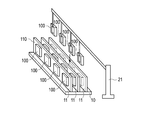
移載装置20における基板100の移載作業は、例えば図4に示すようなロボットアーム21によって行われる。即ち、基板回収時においては、基板キャリア10に装着された基板100を真空吸着などによってロボットアーム21で保持する。その後、ロボットアーム21を移動させて基板キャリア10から基板100を回収し、基板100を基板トレイ200に格納する。また、基板装着時においては、ロボットアーム21によって基板100を基板トレイ200から取り出す。そして、基板100を基板キャリア10上に配置した後にロボットアーム21が基板100を離して、基板キャリア10に基板100が装着される。なお、図4に示したように、移載装置20は、複数の基板100を基板装着面110に同時に装着することが可能である。
処理装置30は、例えば図5に示すような、基板取込室31、処理室32、基板取出室33からなるインライン式製造装置などである。処理室32において、例えば成膜処理、エッチング処理、スパッタ処理などが行われる。
図5に示した処理装置30では、基板100が装着された基板キャリア10が基板取込室31に取り込まれる。そして、基板キャリア10が基板取込室31から処理室32に搬送され、処理室32において所定の処理が行われる。例えば処理室32において基板100に薄膜が形成された後、基板キャリア10は処理室32から基板取出室33に搬送される。その後、基板取出室33から基板キャリア10が取り出される、なお、処理装置30が、基板取出室33を備えない、基板取込室31と処理室32からなる構造であってもよい。
例えば処理装置30がプラズマ化学気相成長(CVD)成膜装置である場合には、基板キャリア10はアノード電極として使用される。処理室32内に原料ガスを導入後、基板キャリア10とカソード電極間に電力を供給して原料ガスをプラズマ状態にする。形成されたプラズマに基板100を曝すことにより、原料ガスに含まれる原料を主成分とする所望の薄膜が基板100の露出した表面に形成される。原料ガスを適宜選択することによって、シリコン半導体薄膜、シリコン窒化薄膜、シリコン酸化薄膜、シリコン酸窒化薄膜、カーボン薄膜などの所望の薄膜を基板100上に形成することができる。例えば、基板100が太陽電池セルである場合に、アンモニア(NH3)ガスとシラン(SiH4)ガスの混合ガスを用いて、基板100上に反射防止膜や絶縁膜として窒化シリコン(SiN)膜を形成できる。
太陽電池反射防止膜の成膜処理などでは、処理対象の基板100の温度を予め決められた設定温度にした状態で、基板100に膜を形成する。このため、処理装置30で成膜処理する場合には、処理室32に搬入される前に、基板取込室31において基板100は予備加熱される。つまり、基板取込室31は予備加熱室を兼ねる。そして、設定温度に達した基板100が処理室32に搬入され、成膜処理が行われる。
基板装着センサ50は、基板キャリア10に基板100が正常な姿勢で装着されていることや、基板キャリア10の正常な位置に基板100が装着されていることを検出する。
基板装着センサ50は、例えば図6に示すように、基板100が装着された基板プレート11の基板装着面110を撮影して判定用画像を取得する画像取得装置501と、判定用画像に基づいて基板100が基板装着面110に正常に装着されているか否かを判定する判定装置502とを備える。
画像取得装置501は、基板100が搭載された基板キャリア10について、搬送装置40上を移動して撮影範囲に入ったときに、基板装着面110上の基板装着領域111を含む画像を撮影する。これにより、基板装着領域111に対する位置基板100の位置や姿勢を判別できる画像が撮影される。判定装置502は、画像取得装置501が撮影した画像について画像処理を行って基板100の位置や姿勢を判別する。そして、設定された基板装着領域111の位置に基板100が配置されていない場合に、判定装置502は基板100が基板装着面110に正常に装着されていないと判定する。
判定装置502は、例えば判定用画像の所定の位置に基板100の画像が存在していない場合に、基板キャリア10に基板100が正常に装着されていないと判定する。画像取得装置501には、例えばCCD(電荷結合素子)カメラやCMOS(相補型金属酸化膜半導体)カメラなどを採用可能である。
なお、図6では、基板装着センサ50が2つの画像取得装置501を有し、基板プレート11の対向する2つの基板装着面110を同時に撮影する例を示した。これにより、基板プレート11の両面において基板100の装着を同時に検出できる。一方、基板プレート11の片方の主面のみが基板装着面110である場合には、1つの画像取得装置501によって、その基板装着面110において基板100の装着を検出する。
また、基板装着センサ50が、撮像装置以外の手段を用いて、基板100が基板装着面110に正常に装着されているか否かを判定してもよい。例えば、反射型の光センサなどの検出装置も基板装着センサ50に採用可能である。
基板キャリア10に基板100が正常に装着されていないことが基板装着センサ50によって検出された場合には、例えば搬送装置40から基板キャリア10を取り出して基板100の移載をやり直す。図1に示した例では、基板100が正常に装着されていないことが搬出側基板装着センサ51によって検出された基板キャリア10は、第1の修正用搬送路61を経由して搬送装置40から取り出される。また、基板100が正常に装着されていないことが搬入側基板装着センサ52によって検出された基板キャリア10は、第2の修正用搬送路62を経由して搬送装置40から取り出される。搬送装置40から取り出された基板キャリア10については、例えば作業者によって基板100の移載のやり直しが行われる。
上記のように、基板処理システム1によれば、基板100が正常に装着されていない基板キャリア10が移載装置20や処理装置30に搬入されることを防止できる。
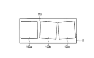
基板キャリア10での基板100の移載時において基板100が正常な位置に装着されなかったり、基板100が正常な姿勢で装着されなかったりした場合には、処理装置30で不具合が生じるおそれがある。図7に、基板100aが基板装着面110に正常な姿勢で装着され、基板100b、100cが基板装着面110に正常な姿勢で装着されていない例を示した。また、図8に、基板装着面110の正常な位置に装着されている基板100dに対し、基板装着面110に密着していない基板100eや基板装着面110から脱落している基板100fの例を示す。
基板キャリア10に基板100が正常に装着されなかった場合には、例えば処理装置30内で基板100が基板キャリア10から落下することによって、基板100が破損したり、処理装置30内の搬送機構が破壊されることがある。また、処理装置30が下方から成膜用のガスが内部に噴射される成膜装置である場合に、ガスの吹き出し口が落下した基板100によって塞がれたり、ガスの流れが乱されたりすることによって、正常な処理を行えないことがある。更に、基板100と隣接する基板プレート11間の距離が設定された値からずれることによって、正常な処理が行えない場合がある。
これに対し、基板処理システム1では、搬出側基板装着センサ51が、移載装置20から搬出されて処理装置30に搬入される前の基板キャリア10について、基板100が正常に装着されていることを検出する。これにより、基板100が基板キャリア10に正常に装着されていないことに起因する処理装置30の故障や自動運転の停止を防止できる。
なお、搬出側基板装着センサ51は、第1の搬送路41上を搬送される基板キャリア10の基板装着面110を撮影可能な位置に配置される。例えば、移載装置10から処理装置30に基板キャリア10が搬送される途中で第1の搬送路41の周囲に配置される。搬出側基板装着センサ51は処理装置30内に配置されるのではないため、周囲が真空状態になることなどを考慮する必要はない。また、基板キャリア10が第1の搬送路41を移動してくるため、基板装着センサ50の位置を固定しておいても、基板キャリア10の基板装着面110を順次撮影することができる。
また、基板装着領域111に基板100が装着されていない状態や、基板100が正常に装着されずに基板装着領域111の一部が露出している状態で基板キャリア10が成膜処理に使用されると、基板装着領域111に膜が形成される。通常、基板100は基板装着面110に配置された固定ピンによって支持されるが、基板装着領域111上に膜が累積的に形成されることによって、固定ピンの基板装着領域111上に露出した部分の長さが短くなる。このため、固定ピンによって基板100を支持できなくなって、基板100を基板キャリア10に装着できない状態になる。
また、基板装着領域111上に膜が形成されると、基板キャリア10を電極として用いるプラズマ成膜装置などでは、基板キャリア10の表面が膜によって絶縁される結果、基板キャリア10と基板100間の電気的接続が劣化する。これにより基板100が電気的にフローティング状態となって、成膜速度の低下、膜厚の均一性の低下などの問題が生じる。
しかし、基板装着センサ50が、基板キャリア10に定義されたすべての基板装着領域111に基板が装着されていることを検出することにより、基板装着領域111に膜が形成されることを防止できる。基板キャリア10のすべての基板装着領域111に基板が装着されていることを検出するためには、例えば、基板装着領域111のそれぞれが画像取得装置501の撮影範囲に入ってきたタイミングで、基板装着領域111について一つずつ画像を撮影する。或いは、画像取得装置501に広角レンズを使用して、すべての基板装着領域111を同時に撮影してもよい。
また、処理装置30での処理工程において、基板キャリア10から基板100が外れたり、基板装着面110上の基板100の姿勢が乱れたりすることがある。例えば、処理装置30での処理において加熱された基板100に反りが生じて、基板100の位置が基板装着領域111からずれたり、基板100の姿勢が乱れたりする場合がある。この状態で基板キャリア10が移載装置20に搬入されて移載作業が行われると、基板100が基板キャリア10から落下して破損したり、ロボットアーム21が基板100を正確に保持することができない。
また、基板装着領域111に基板100が装着されていない状態で基板キャリア10が処理装置30から移載装置20に搬送された場合に、基板100が装着されていない基板装着領域111をロボットアーム21が吸着することがある。その結果、ロボットアーム21によって基板キャリア10が引っ張られ、基板キャリア10が搬送装置40から外れたり、基板キャリア10から基板100が落下するなどの障害が発生したりする。
これに対し、基板処理システム1では、搬入側基板装着センサ52が、処理装置30から搬出されて移載装置20に搬入される前の基板キャリア10について、基板100が正常に装着されていることを検出する。これにより、基板100が基板キャリア10に正常に装着されていないことに起因する移載装置20の故障や自動運転の停止を防止できる。搬入側基板装着センサ52は、第2の搬送路42上を搬送される基板キャリア10の基板装着面110を撮影可能な位置に配置される。例えば、処理装置30から移載装置10に基板キャリア10が搬送される途中で第2の搬送路42の周囲に配置される。搬出側基板装着センサ51と同様に搬入側基板装着センサ52は処理装置30内に配置されるのではないため、周囲が真空状態になることなどを考慮する必要はない。また、基板キャリア10が第2の搬送路42を移動してくるため、画像取得装置501の位置を固定しておいても、基板キャリア10の基板装着面110を順次撮影することができる。
以上に説明したように、本発明の実施形態に係る基板処理システム1では、移載装置20から搬出された直後や移載装置20に搬入される直前において、基板キャリア10に基板100が正常に装着されていることが検出される。その結果、図1に示した基板処理システム1によれば、基板100が正常に基板キャリア10に装着されていないことに起因する障害を抑制することができる。
なお、図1では基板処理システム1が、搬出側基板装着センサ51と搬入側基板装着センサ52を備える場合を示した。しかし、移載装置20に基板キャリア10が搬入される位置と、移載装置20から基板キャリア10が搬出される位置の、いずれか一方だけに基板装着センサ50を配置してもよい。例えば、処理装置30内において基板装着面110上で基板100の位置が変動するおそれがない場合には、移載装置20に基板キャリア10が搬入される位置には基板装着センサ50を配置しなくてもよい。
(その他の実施形態)
上記のように、本発明は実施形態によって記載したが、この開示の一部をなす論述及び図面はこの発明を限定するものであると理解すべきではない。この開示から当業者には様々な代替実施形態、実施例及び運用技術が明らかとなろう。
上記のように、本発明は実施形態によって記載したが、この開示の一部をなす論述及び図面はこの発明を限定するものであると理解すべきではない。この開示から当業者には様々な代替実施形態、実施例及び運用技術が明らかとなろう。
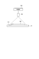
上記では、基板キャリア10が基板100を垂直に装着するボートタイプである例を示したが、他のタイプの基板キャリア10にも本発明を適用することが可能である。例えば基板キャリア10が、水平方向に延伸する基板装着面110に基板100を水平に装着するカートタイプであってもよい。カートタイプの基板キャリア10の場合には、例えば図9に示すように、上方から画像取得装置501によって基板装着面110を撮影することにより、基板キャリア10に基板100が正常に装着されていることを基板装着センサ50が検出する。
このように、本発明はここでは記載していない様々な実施形態等を含むことは勿論である。したがって、本発明の技術的範囲は上記の説明から妥当な請求の範囲に係る発明特定事項によってのみ定められるものである。
本発明は、基板キャリアを用いる基板処理システムに利用可能である。
Claims (7)
- 基板を基板キャリアに移載する移載装置と、
前記基板キャリアに装着された前記基板を処理対象とする処理装置と、
前記移載装置と前記処理装置間で前記基板キャリアを搬送する搬送装置と、
前記移載装置と前記処理装置間において、前記基板キャリアに前記基板が正常に装着されているか否かを検出する基板装着センサと
を備えることを特徴とする基板処理システム。 - 前記基板装着センサが、前記移載装置から前記基板キャリアが搬出される位置及び前記移載装置に前記基板キャリアが搬入される位置の少なくともいずれかに配置されていることを特徴とする請求項1に記載の基板処理システム。
- 前記基板装着センサが、前記基板キャリアに前記基板が正常な姿勢で装着されていることを検出することを特徴とする請求項1に記載の基板処理システム。
- 前記基板装着センサが、前記基板キャリアの正常な位置に前記基板が装着されていることを検出することを特徴とする請求項1に記載の基板処理システム。
- 前記基板装着センサが、前記基板キャリアに定義されたすべての基板装着領域に前記基板が装着されていることを検出することを特徴とする請求項1に記載の基板処理システム。
- 前記移載装置が、
前記処理装置での処理が行われた処理済の前記基板を前記基板キャリアから回収し、
前記処理装置での処理が行われていない未処理の前記基板を前記基板キャリアに装着する
ことを特徴とする請求項1に記載の基板処理システム。 - 前記処理装置が、前記基板上に膜を形成する成膜装置であることを特徴とする請求項1に記載の基板処理システム。
Priority Applications (2)
| Application Number | Priority Date | Filing Date | Title |
|---|---|---|---|
| JP2015512233A JP6103043B2 (ja) | 2013-04-17 | 2013-04-17 | 基板処理システム |
| PCT/JP2013/061355 WO2014170969A1 (ja) | 2013-04-17 | 2013-04-17 | 基板処理システム |
Applications Claiming Priority (1)
| Application Number | Priority Date | Filing Date | Title |
|---|---|---|---|
| PCT/JP2013/061355 WO2014170969A1 (ja) | 2013-04-17 | 2013-04-17 | 基板処理システム |
Publications (1)
| Publication Number | Publication Date |
|---|---|
| WO2014170969A1 true WO2014170969A1 (ja) | 2014-10-23 |
Family
ID=51730942
Family Applications (1)
| Application Number | Title | Priority Date | Filing Date |
|---|---|---|---|
| PCT/JP2013/061355 Ceased WO2014170969A1 (ja) | 2013-04-17 | 2013-04-17 | 基板処理システム |
Country Status (2)
| Country | Link |
|---|---|
| JP (1) | JP6103043B2 (ja) |
| WO (1) | WO2014170969A1 (ja) |
Citations (3)
| Publication number | Priority date | Publication date | Assignee | Title |
|---|---|---|---|---|
| JPH03270253A (ja) * | 1990-03-20 | 1991-12-02 | Tokyo Electron Sagami Ltd | ウエハ処理方法およびウエハ処理装置 |
| JPH073947A (ja) * | 1993-06-16 | 1995-01-06 | Kajima Corp | 炭素繊維強化プラスチック製ストランドの定着方法 |
| JPH1012707A (ja) * | 1996-06-24 | 1998-01-16 | Kokusai Electric Co Ltd | ボートに於けるウェーハ位置ずれ補正装置 |
Family Cites Families (7)
| Publication number | Priority date | Publication date | Assignee | Title |
|---|---|---|---|---|
| JPS629204A (ja) * | 1985-07-05 | 1987-01-17 | Sumitomo Electric Ind Ltd | プリント基板の位置決め方法 |
| JPH0473947A (ja) * | 1990-07-16 | 1992-03-09 | Tokyo Electron Sagami Ltd | ウエハ移し換え方法 |
| DE19814046C1 (de) * | 1998-03-30 | 1999-11-18 | Jenoptik Jena Gmbh | Anordnung zur Detektion von scheibenförmigen Objekten in einer Kassette |
| JP2000174103A (ja) * | 1998-12-01 | 2000-06-23 | Yamatake Corp | 板状部材存在状態検出装置 |
| JP2001185502A (ja) * | 1999-12-22 | 2001-07-06 | Mitsubishi Electric Corp | 半導体素子製造工程における不純物拡散方法、同方法に用いる不純物拡散装置および同方法から製造された半導体素子 |
| JP5343326B2 (ja) * | 2007-05-29 | 2013-11-13 | 株式会社ニコン | 基板接合装置および基板接合方法 |
| JP2009302392A (ja) * | 2008-06-16 | 2009-12-24 | Kawasaki Heavy Ind Ltd | 基板検出装置および方法 |
-
2013
- 2013-04-17 WO PCT/JP2013/061355 patent/WO2014170969A1/ja not_active Ceased
- 2013-04-17 JP JP2015512233A patent/JP6103043B2/ja not_active Expired - Fee Related
Patent Citations (3)
| Publication number | Priority date | Publication date | Assignee | Title |
|---|---|---|---|---|
| JPH03270253A (ja) * | 1990-03-20 | 1991-12-02 | Tokyo Electron Sagami Ltd | ウエハ処理方法およびウエハ処理装置 |
| JPH073947A (ja) * | 1993-06-16 | 1995-01-06 | Kajima Corp | 炭素繊維強化プラスチック製ストランドの定着方法 |
| JPH1012707A (ja) * | 1996-06-24 | 1998-01-16 | Kokusai Electric Co Ltd | ボートに於けるウェーハ位置ずれ補正装置 |
Also Published As
| Publication number | Publication date |
|---|---|
| JPWO2014170969A1 (ja) | 2017-02-16 |
| JP6103043B2 (ja) | 2017-03-29 |
Similar Documents
| Publication | Publication Date | Title |
|---|---|---|
| JP7678077B2 (ja) | 処理システムのアライナステーションの較正 | |
| CN110690095B (zh) | 处理边缘环的方法、基底处理系统和图像传感器 | |
| JP6156513B2 (ja) | 基板処理システム | |
| US11414740B2 (en) | Processing system for forming layers | |
| KR20160124965A (ko) | 웨이퍼 이송 장치 | |
| CN110678962A (zh) | 处理条件设定方法、存储介质和基板处理系统 | |
| CN115326817B (zh) | 基板检查方法和基板检查装置 | |
| CN109273385A (zh) | 基于机械臂的晶圆缺陷检测方法、机械臂、半导体设备 | |
| KR102947111B1 (ko) | 기판 반송 시스템 및 화상 보정 방법 | |
| JP6103043B2 (ja) | 基板処理システム | |
| TWI853051B (zh) | 放置載體的載體前開式晶圓傳送盒及方法 | |
| JP5606546B2 (ja) | ワーク処理装置 | |
| CN113871329A (zh) | 基板处理装置和基板处理方法 | |
| JP5999268B2 (ja) | 基板装着姿勢判定装置及び基板装着姿勢判定方法 | |
| KR102344253B1 (ko) | 사이드 스토리지 유닛 및 이를 구비하는 기판 처리 시스템 | |
| CN110416137B (zh) | 用于半导体工艺的基板传送机构及成膜系统 | |
| JP2022042669A (ja) | 搬送システム | |
| KR102304254B1 (ko) | 영상 기법을 이용한 트레이 검사 장치 | |
| JP6065110B2 (ja) | 基板処理システム | |
| JP2000252335A (ja) | 半導体製造装置 | |
| TW202534853A (zh) | 基板移動系統 | |
| KR100837546B1 (ko) | 피브이디장비의 웨이퍼 확인장치 및 확인 방법 | |
| KR20260056961A (ko) | 기판 반송 시스템 및 화상 보정 방법 | |
| WO2023176442A1 (ja) | 監視用基板及び監視方法 | |
| KR20250108330A (ko) | 기판 이송 시스템 및 이의 기판 적재 상태 모니터링 방법 |
Legal Events
| Date | Code | Title | Description |
|---|---|---|---|
| 121 | Ep: the epo has been informed by wipo that ep was designated in this application |
Ref document number: 13882112 Country of ref document: EP Kind code of ref document: A1 |
|
| ENP | Entry into the national phase |
Ref document number: 2015512233 Country of ref document: JP Kind code of ref document: A |
|
| NENP | Non-entry into the national phase |
Ref country code: DE |
|
| 122 | Ep: pct application non-entry in european phase |
Ref document number: 13882112 Country of ref document: EP Kind code of ref document: A1 |