WO2014170958A1 - Ledランプ点灯装置、および、ledランプ点灯装置の制御方法 - Google Patents
Ledランプ点灯装置、および、ledランプ点灯装置の制御方法 Download PDFInfo
- Publication number
- WO2014170958A1 WO2014170958A1 PCT/JP2013/061309 JP2013061309W WO2014170958A1 WO 2014170958 A1 WO2014170958 A1 WO 2014170958A1 JP 2013061309 W JP2013061309 W JP 2013061309W WO 2014170958 A1 WO2014170958 A1 WO 2014170958A1
- Authority
- WO
- WIPO (PCT)
- Prior art keywords
- lamp
- circuit
- switch
- contact
- external terminal
- Prior art date
- Legal status (The legal status is an assumption and is not a legal conclusion. Google has not performed a legal analysis and makes no representation as to the accuracy of the status listed.)
- Ceased
Links
Images






















Classifications
-
- H—ELECTRICITY
- H05—ELECTRIC TECHNIQUES NOT OTHERWISE PROVIDED FOR
- H05B—ELECTRIC HEATING; ELECTRIC LIGHT SOURCES NOT OTHERWISE PROVIDED FOR; CIRCUIT ARRANGEMENTS FOR ELECTRIC LIGHT SOURCES, IN GENERAL
- H05B45/00—Circuit arrangements for operating light-emitting diodes [LED]
- H05B45/40—Details of LED load circuits
- H05B45/44—Details of LED load circuits with an active control inside an LED matrix
- H05B45/48—Details of LED load circuits with an active control inside an LED matrix having LEDs organised in strings and incorporating parallel shunting devices
Definitions
- the present invention relates to an LED lamp lighting device and a method for controlling the LED lamp lighting device.
- LED (Light Emitting Diode) lamps can be driven at a low voltage and have longer life, lower power consumption, faster reaction speed, and higher impact resistance than filament lamps (bulb lamps). Therefore, the size and weight can be reduced.
- the LED lamp can be suitably used for, for example, a vehicle headlamp.
- LED lamp driving device for example, there is an LED lighting control device as disclosed in JP 2012-160413 A.
- the LED lighting control device described in Japanese Patent Application Laid-Open No. 2012-160413 can detect an LED open error with a simple circuit configuration and determine an LED voltage that does not cause the LED open error.
- An LED lamp lighting device Connected between a first power supply terminal on the low potential side and a second power supply terminal on the high potential side of the lamp drive power supply, receives a drive current from the lamp drive power supply, and is connected in series by the drive current.
- An LED lamp lighting device for lighting a plurality of LED lamps, A first external terminal connected to the first power supply terminal; A second external terminal connected to the second power supply terminal; A first lamp circuit comprising one LED lamp or a plurality of LED lamps connected in series, one end of which is connected to the first external terminal; A second lamp circuit composed of one LED lamp or a plurality of LED lamps connected in series, one end of which is connected to the other end of the first lamp circuit; A third lamp having one LED lamp or a plurality of LED lamps connected in series, one end connected to the other end of the second lamp circuit and the other end connected to the second external terminal Circuit, Between a first reference node and a first contact connected to the first external terminal, or a second reference node and a second contact connected to the other end of the first ramp circuit.
- a first switch circuit that conducts only one of the contacts of Between a second reference node connected to the other end of the first ramp circuit and a third contact connected to the first reference node, or between the second reference node and a fourth A second switch circuit that conducts only one of the contacts; Between the third reference node connected to the first reference node and the fifth contact connected to the second external terminal, between the third reference node and the sixth contact Or a third switch circuit that conducts only one of the third reference node and a seventh contact connected to the other end of the second ramp circuit; A diode having a cathode connected to the other end of the second ramp circuit and an anode connected to the fourth contact; A switching element having one end connected to the fourth contact and the other end connected to the second external terminal; A switch control circuit for controlling the switch element in accordance with a potential difference between the fourth contact and the second external terminal;
- the switch control circuit includes: When the magnitude of the potential difference between the fourth contact and the second external terminal is equal to or higher than a preset reference voltage, the switch
- the first lamp circuit, the second lamp circuit, and the third lamp circuit are extinguished by short-circuiting between the first external terminal and the second external terminal.
- the switch element is a thyristor having a cathode connected to the fourth contact and an anode connected to the second external terminal.
- the switch control circuit includes: A first resistor having one end connected to the fourth contact and the other end connected to the gate of the thyristor; A second resistor having one end connected to the other end of the first resistor; A Zener diode having an anode connected to the other end of the second resistor and a cathode connected to the second external terminal.
- the lamp driving power source is A first input terminal connected to one end of the alternator; A second input terminal connected to the other end of the AC generator; A power switch element having one end connected to the first input terminal and the other end connected to the first power terminal; A capacitor having one end connected to the other end of the power switch element and the other end connected to the second input terminal; A detection resistor having one end connected to the second input terminal and the other end connected to the second power supply terminal; When the current flows through the detection resistor, the power switch element is controlled so that the current flowing through the detection resistor is constant. On the other hand, when the current does not flow through the detection resistor, the first resistor A drive control circuit that controls the power switch element so that a voltage between a power supply terminal and the second power supply terminal is a predetermined voltage set in advance.
- the power switch element is a thyristor having a cathode connected to the first input terminal, an anode connected to the first power supply terminal, and a gate to which a control signal is input from the drive control circuit.
- the lamp driving power source is It has a constant voltage control function and a constant current control function, When a current can be supplied to any one of the first lamp circuit, the second lamp circuit, and the third lamp circuit, a constant current is supplied to the LED lamp by the constant current control function. , When no current can flow through any of the LED lamps in the first lamp circuit, the second lamp circuit, and the third lamp circuit, the constant voltage control function causes the first power supply terminal to The output voltage output between the second power supply terminal is raised to a predetermined voltage set in advance and limited to a constant voltage.
- the one end of the first lamp circuit is a cathode side of the LED lamp of the first lamp circuit;
- the other end of the first lamp circuit is an anode side of the LED lamp of the first lamp circuit;
- the one end of the second lamp circuit is a cathode side of the LED lamp of the second lamp circuit;
- the other end of the second lamp circuit is an anode side of the LED lamp of the second lamp circuit;
- the one end of the third lamp circuit is a cathode side of the LED lamp of the third lamp circuit;
- the other end of the third lamp circuit is an anode side of the LED lamp of the third lamp circuit.
- the first switch circuit, the second switch circuit, and the third switch circuit are manually controlled by a user.
- the LED lamp of the first lamp circuit is a high beam lamp of a vehicle headlamp
- the LED lamp of the second lamp circuit is a low beam lamp of the headlamp
- the LED lamp of the third lamp circuit is a position lamp of the vehicle.
- the control method of the LED lamp lighting device includes: Connected between a first power supply terminal on the low potential side and a second power supply terminal on the high potential side of the lamp drive power supply, receives a drive current from the lamp drive power supply, and is connected in series by the drive current.
- An LED lamp lighting device for lighting a plurality of LED lamps, a first external terminal connected to the first power supply terminal, a second external terminal connected to the second power supply terminal, A first lamp circuit composed of one LED lamp or a plurality of LED lamps connected in series, one end of which is connected to the first external terminal, and one LED lamp or a plurality of LEDs connected in series A second lamp circuit having one end connected to the other end of the first lamp circuit, and one LED lamp or a plurality of LED lamps connected in series, and one end being the second lamp circuit.
- Lamp circuit Between a third ramp circuit connected to the other end, the other end connected to the second external terminal, a first reference node, and a first contact connected to the first external terminal Or a first switch circuit that conducts only one of the first reference node and a second contact connected to the other end of the first ramp circuit, and the first switch circuit. Between the second reference node connected to the other end of the ramp circuit and the third contact connected to the first reference node, or between the second reference node and the fourth contact A second switch circuit that conducts only one of them, a third reference node connected to the first reference node, and a fifth contact connected to the second external terminal. Or between the third reference node and the sixth contact, or between the third reference node and the second ramp circuit.
- a third switch circuit that conducts only one of the seventh contact connected to the other end, a cathode connected to the other end of the second ramp circuit, and an anode connected to the fourth contact
- a switch element having one end connected to the fourth contact and the other end connected to the second external terminal; and between the fourth contact and the second external terminal.
- a switch control circuit for controlling the switch element in accordance with the potential difference of the LED lamp lighting device comprising: When the magnitude of the potential difference between the fourth contact and the second external terminal is equal to or higher than a preset reference voltage, the switch element is turned on, When the magnitude of the potential difference between the fourth contact and the second external terminal is less than the reference voltage, the switch element is turned off.
- An LED lamp driving device is connected between a low-potential-side first power supply terminal and a high-potential-side second power supply terminal of a lamp drive power supply.
- the plurality of LED lamps connected in series with the drive current are turned on by the supply.
- the LED lamp lighting device includes a first external terminal connected to the first power supply terminal, a second external terminal connected to the second power supply terminal, and a plurality of LED lamps connected in series.
- the first lamp circuit is composed of an LED lamp, one end of which is connected to the first external terminal, and one LED lamp or a plurality of LED lamps connected in series, and one end of the first lamp circuit.
- a second lamp circuit connected to the other end and one LED lamp or a plurality of LED lamps connected in series, with one end connected to the other end of the second lamp circuit and the other end being the second.
- a third ramp circuit connected to the external terminal of the first, a first reference node, and a first contact connected to the first external terminal, or a first reference node, Any one between the second contact point connected to the other end of the ramp circuit Between a first switch circuit conducting only one, a second reference node connected to the other end of the first ramp circuit, and a third contact connected to the first reference node, or ,
- a second switch circuit that conducts only one of the second reference node and the fourth contact point, a third reference node connected to the first reference node, and a second external Between the fifth contact connected to the terminal, between the third reference node and the sixth contact, or between the third reference node and the other end of the second ramp circuit.
- a third switch circuit that conducts only one of the first and second contacts, a diode having a cathode connected to the other end of the second lamp circuit, an anode connected to the fourth contact, and one end Is connected to the fourth contact and the other end is connected to the second external terminal, the fourth contact and the second contact According to the potential difference between the external terminal comprises a switch control circuit for controlling the switching element.
- the switch control circuit turns on the switch element when the magnitude of the potential difference between the fourth contact and the second external terminal is equal to or higher than a preset reference voltage, When the magnitude of the potential difference with the second external terminal is less than the reference voltage, the switch element is turned off.
- the LED lamp lighting device according to the present invention can operate in the same manner as a conventional general bulb lamp lighting device.
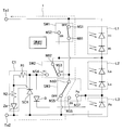
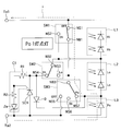
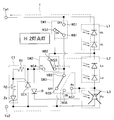
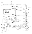
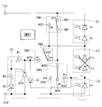
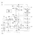
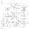
- FIG. 1 is a circuit diagram illustrating an example of a configuration of an LED lamp lighting device according to a first embodiment which is an aspect of the present invention.
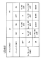
- FIG. 2 is a diagram showing a relationship between on / off of each switch of a general bulb lamp lighting device and lighting of each bulb lamp.
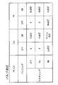
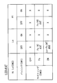
- FIG. 3 is a diagram illustrating a relationship between on / off of each switch of the lamp lighting device 100 according to the first embodiment illustrated in FIG. 1 and lighting of each LED lamp.
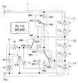
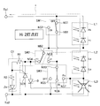
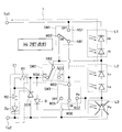
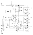
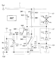
- FIG. 4 is a circuit diagram illustrating an example of an operation during a normal operation in which the LED lamp of the lamp lighting device 100 according to the first embodiment illustrated in FIG. 1 has not failed.
- FIG. 1 is a circuit diagram illustrating an example of a configuration of an LED lamp lighting device according to a first embodiment which is an aspect of the present invention.
- FIG. 2 is a diagram showing a relationship between on / off of each switch of a general bulb lamp lighting device and lighting of each bulb lamp.
- FIG. 3 is a diagram illustrating a relationship
- FIG. 5 is a circuit diagram illustrating an example of an operation during a normal operation in which the LED lamp of the lamp lighting device 100 according to the first embodiment illustrated in FIG. 1 is not malfunctioning.
- FIG. 6 is a circuit diagram illustrating an example of an operation during normal operation in which the LED lamp of the lamp lighting device 100 according to the first embodiment illustrated in FIG.
- FIG. 7 is a circuit diagram illustrating an example of an operation during a normal operation in which the LED lamp of the lamp lighting device 100 according to the first embodiment illustrated in FIG. 1 is not malfunctioning.
- FIG. 8 is a circuit diagram illustrating an example of an operation during a normal operation in which the LED lamp of the lamp lighting device 100 according to the first embodiment illustrated in FIG. FIG.
- FIG. 9 is a circuit diagram illustrating an example of an operation during a normal operation in which the LED lamp of the lamp lighting device 100 according to the first embodiment illustrated in FIG. 1 is not malfunctioning.
- FIG. 10 is a circuit diagram illustrating an example of an operation during a normal operation in which the LED lamp of the lamp lighting device 100 according to the first embodiment illustrated in FIG.
- FIG. 11 is a circuit diagram illustrating an example of operation during normal operation in which the LED lamp of the lamp lighting device 100 according to the first embodiment illustrated in FIG.
- FIG. 12 is a circuit diagram illustrating an example of an operation during a normal operation in which the LED lamp of the lamp lighting device 100 according to the first embodiment illustrated in FIG. FIG.
- FIG. 13 is a circuit diagram illustrating an example of an operation during a normal operation in which the LED lamp of the lamp lighting device 100 according to the first embodiment illustrated in FIG. 1 is not malfunctioning.
- FIG. 14 is a circuit diagram illustrating an example of an operation during a normal operation in which the LED lamp of the lamp lighting device 100 according to the first embodiment illustrated in FIG. 1 is not malfunctioning.
- FIG. 15 is a circuit diagram illustrating an example of operation during normal operation in which the LED lamp of the lamp lighting device 100 according to the first embodiment illustrated in FIG.
- FIG. 16 is a diagram showing a relationship between on / off of each switch of a general bulb lamp lighting device and lighting of each bulb lamp when the position lamp Po is out of order.
- FIG. 17 is a diagram illustrating a relationship between on / off of each switch of the lamp lighting device 100 according to the first embodiment illustrated in FIG. 1 and lighting of each LED lamp when the position lamp Po is out of order.
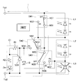
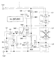
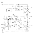
- FIG. 18 is a circuit diagram illustrating an example of an operation when the position lamp Po of the lamp lighting device 100 according to the first embodiment illustrated in FIG. 1 is out of order.
- FIG. 19 is a circuit diagram showing an example of the operation when the position lamp Po of the lamp lighting device 100 according to the first embodiment shown in FIG. 1 is out of order.
- FIG. 20 is a circuit diagram illustrating an example of the operation when the position lamp Po of the lamp lighting device 100 according to the first embodiment illustrated in FIG. 1 is out of order.
- FIG. 20 is a circuit diagram illustrating an example of the operation when the position lamp Po of the lamp lighting device 100 according to the first embodiment illustrated in FIG. 1 is out of order.
- FIG. 21 is a circuit diagram showing an example of the operation when the position lamp Po of the lamp lighting device 100 according to the first embodiment shown in FIG. 1 is out of order.
- FIG. 22 is a circuit diagram illustrating an example of an operation when the position lamp Po of the lamp lighting device 100 according to the first embodiment illustrated in FIG. 1 is out of order.
- FIG. 23 is a circuit diagram illustrating an example of the operation when the position lamp Po of the lamp lighting device 100 according to the first embodiment illustrated in FIG. 1 is out of order.
- FIG. 24 is a circuit diagram illustrating an example of an operation when the position lamp Po of the lamp lighting device 100 according to the first embodiment illustrated in FIG. 1 is out of order.
- FIG. 22 is a circuit diagram illustrating an example of an operation when the position lamp Po of the lamp lighting device 100 according to the first embodiment illustrated in FIG. 1 is out of order.
- FIG. 23 is a circuit diagram illustrating an example of the operation when the position lamp Po of the lamp lighting device 100 according to the first embodiment illustrated in FIG. 1 is out of order
- FIG. 25 is a circuit diagram illustrating an example of an operation when the position lamp Po of the lamp lighting device 100 according to the first embodiment illustrated in FIG. 1 is out of order.
- FIG. 26 is a circuit diagram illustrating an example of the operation when the position lamp Po of the lamp lighting device 100 according to the first embodiment illustrated in FIG. 1 is out of order.
- FIG. 27 is a circuit diagram showing an example of the operation when the position lamp Po of the lamp lighting device 100 according to the first embodiment shown in FIG. 1 is out of order.
- FIG. 28 is a circuit diagram illustrating an example of the operation when the position lamp Po of the lamp lighting device 100 according to the first embodiment illustrated in FIG. 1 is out of order.
- FIG. 28 is a circuit diagram illustrating an example of the operation when the position lamp Po of the lamp lighting device 100 according to the first embodiment illustrated in FIG. 1 is out of order.
- FIG. 29 is a circuit diagram illustrating an example of an operation when the position lamp Po of the lamp lighting device 100 according to the first embodiment illustrated in FIG. 1 is out of order.
- FIG. 30 is a diagram showing a relationship between on / off of each switch of a general bulb lamp lighting device and lighting of each bulb lamp when the low beam lamp Lo is out of order.
- FIG. 31 is a diagram illustrating a relationship between on / off of each switch of the lamp lighting device 100 according to the first embodiment illustrated in FIG. 1 and lighting of each LED lamp when the low beam lamp Lo is malfunctioning. .
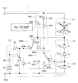
- FIG. 32 is a circuit diagram illustrating an example of the operation when the low beam lamp Lo of the lamp lighting device 100 according to the first embodiment illustrated in FIG. 1 is out of order.
- FIG. 30 is a diagram showing a relationship between on / off of each switch of a general bulb lamp lighting device and lighting of each bulb lamp when the low beam lamp Lo is out of order.
- FIG. 31 is a diagram illustrating a relationship between on / off of each
- FIG. 33 is a circuit diagram showing an example of the operation when the low beam lamp Lo of the lamp lighting device 100 according to the first embodiment shown in FIG. 1 is out of order.
- FIG. 34 is a circuit diagram showing an example of the operation when the low beam lamp Lo of the lamp lighting device 100 according to the first embodiment shown in FIG. 1 is out of order.
- FIG. 35 is a circuit diagram illustrating an example of the operation when the low beam lamp Lo of the lamp lighting device 100 according to the first embodiment illustrated in FIG. 1 is out of order.
- FIG. 36 is a circuit diagram showing an example of the operation when the low beam lamp Lo of the lamp lighting device 100 according to the first embodiment shown in FIG. 1 is out of order.
- FIG. 34 is a circuit diagram showing an example of the operation when the low beam lamp Lo of the lamp lighting device 100 according to the first embodiment shown in FIG. 1 is out of order.
- FIG. 35 is a circuit diagram illustrating an example of the operation when the low beam lamp Lo of the lamp lighting device 100 according to the first embodiment illustrated in FIG. 1 is
- FIG. 37 is a circuit diagram showing an example of the operation when the low beam lamp Lo of the lamp lighting device 100 according to the first embodiment shown in FIG. 1 is out of order.
- FIG. 38 is a circuit diagram illustrating an example of an operation when the low beam lamp Lo of the lamp lighting device 100 according to the first embodiment illustrated in FIG. 1 is out of order.
- FIG. 39 is a circuit diagram showing an example of the operation when the low beam lamp Lo of the lamp lighting device 100 according to the first embodiment shown in FIG. 1 is out of order.
- FIG. 40 is a circuit diagram illustrating an example of the operation when the low beam lamp Lo of the lamp lighting device 100 according to the first embodiment illustrated in FIG. 1 is out of order.
- FIG. 38 is a circuit diagram illustrating an example of an operation when the low beam lamp Lo of the lamp lighting device 100 according to the first embodiment illustrated in FIG. 1 is out of order.
- FIG. 39 is a circuit diagram showing an example of the operation when the low beam lamp Lo of the lamp lighting device 100 according to the first embodiment shown in FIG. 1
- FIG. 41 is a circuit diagram illustrating an example of the operation when the low beam lamp Lo of the lamp lighting device 100 according to the first embodiment illustrated in FIG. 1 is out of order.
- FIG. 42 is a circuit diagram illustrating an example of the operation when the low beam lamp Lo of the lamp lighting device 100 according to the first embodiment illustrated in FIG. 1 is out of order.
- FIG. 43 is a circuit diagram illustrating an example of the operation when the low beam lamp Lo of the lamp lighting device 100 according to the first embodiment illustrated in FIG. 1 is out of order.
- FIG. 44 is a diagram showing a relationship between on / off of each switch of a general bulb lamp lighting device and lighting of each bulb lamp when the high beam lamp Hi is out of order.
- FIG. 42 is a circuit diagram illustrating an example of the operation when the low beam lamp Lo of the lamp lighting device 100 according to the first embodiment illustrated in FIG. 1 is out of order.
- FIG. 43 is a circuit diagram illustrating an example of the operation when the low beam lamp Lo of the lamp lighting device 100 according to the first embodiment
- FIG. 45 is a diagram illustrating a relationship between on / off of each switch of the lamp lighting device 100 according to the first embodiment illustrated in FIG. 1 and lighting of each LED lamp when the high beam lamp Hi is out of order.
- FIG. 46 is a circuit diagram showing an example of the operation when the high beam lamp Hi of the lamp lighting device 100 according to the first embodiment shown in FIG. 1 is out of order.
- FIG. 47 is a circuit diagram showing an example of the operation when the high beam lamp Hi of the lamp lighting device 100 according to the first embodiment shown in FIG. 1 is out of order.
- FIG. 48 is a circuit diagram showing an example of operation when the high beam lamp Hi of the lamp lighting device 100 according to the first embodiment shown in FIG. 1 is out of order.
- FIG. 46 is a circuit diagram showing an example of the operation when the high beam lamp Hi of the lamp lighting device 100 according to the first embodiment shown in FIG. 1 is out of order.
- FIG. 49 is a circuit diagram showing an example of the operation when the high beam lamp Hi of the lamp lighting device 100 according to the first embodiment shown in FIG. 1 is out of order.
- FIG. 50 is a circuit diagram illustrating an example of an operation when the high beam lamp Hi of the lamp lighting device 100 according to the first embodiment illustrated in FIG. 1 is out of order.
- FIG. 51 is a circuit diagram showing an example of the operation when the high beam lamp Hi of the lamp lighting device 100 according to the first embodiment shown in FIG. 1 is out of order.
- FIG. 52 is a circuit diagram showing an example of the operation when the high beam lamp Hi of the lamp lighting device 100 according to the first embodiment shown in FIG. 1 is out of order.
- FIG. 50 is a circuit diagram illustrating an example of an operation when the high beam lamp Hi of the lamp lighting device 100 according to the first embodiment illustrated in FIG. 1 is out of order.
- FIG. 51 is a circuit diagram showing an example of the operation when the high beam lamp Hi of the lamp lighting device 100 according to the first embodiment shown in FIG. 1 is
- FIG. 53 is a circuit diagram showing an example of the operation when the high beam lamp Hi of the lamp lighting device 100 according to the first embodiment shown in FIG. 1 is out of order.
- FIG. 54 is a circuit diagram showing an example of the operation when the high beam lamp Hi of the lamp lighting device 100 according to the first embodiment shown in FIG. 1 is out of order.
- FIG. 55 is a circuit diagram showing an example of operation when the high beam lamp Hi of the lamp lighting device 100 according to the first embodiment shown in FIG. 1 is out of order.
- FIG. 56 is a circuit diagram showing an example of operation when the high beam lamp Hi of the lamp lighting device 100 according to the first embodiment shown in FIG. 1 is out of order.
- FIG. 57 is a circuit diagram showing an example of the operation when the high beam lamp Hi of the lamp lighting device 100 according to the first embodiment shown in FIG. 1 is out of order.
- FIG. 1 is a circuit diagram showing an example of the configuration of an LED lamp lighting device according to a first embodiment which is an aspect of the present invention.
- the example shown in FIG. 1 is an example of a headlamp of a vehicle, for example.
- a lamp driving power source 10 is connected to the LED lamp lighting device 100.
- An AC generator G is connected to the lamp driving power source 10.
- the AC generator G is a single-phase AC generator, and is configured to generate AC power by rotating in conjunction with an engine of a vehicle, for example.
- One end G1 of the AC generator G is connected to the first input terminal TI1 of the lamp driving power source 10, and the other end G2 is grounded.
- the AC generator G is configured to output the generated AC voltage VA to the lamp driving power source 10.
- the first power supply terminal TS1 on the negative voltage side (low potential side) of the lamp driving power supply 10 is connected to the external terminal Ta1 of the LED lamp lighting device 100, and the positive voltage side (high potential side) of the lamp driving power supply 10 is connected.
- the second power supply terminal TS2 is connected to the external terminal Ta2 of the LED lamp lighting device 100.
- the lamp driving power supply 10 supplies the LED lamp driving current to the LED lamp lighting device 100.
- the LED lamp lighting device 100 is connected between the low-potential-side first power supply terminal TS1 and the high-potential-side second power supply terminal TS2 of the lamp drive power supply 10, and the drive current from the lamp drive power supply 10 is reduced.
- a plurality of LED lamps connected in series are lit by the drive current when supplied.
- the LED lamp lighting device 100 includes a first external terminal Ta1, a second external terminal Ta2, a first lamp circuit L1, a second lamp circuit L2, 3 lamp circuit L3, first switch circuit SW1, second switch circuit SW2, third switch circuit SW3, switch element SCR, diode D, and switch control circuit C1.
- the first external terminal Ta1 is connected to the first power supply terminal TS1.
- the second external terminal Ta2 is connected to the second power supply terminal TS2.
- the first lamp circuit L1 includes one LED lamp or a plurality of LED lamps connected in series, and one end is connected to the first external terminal Ta1.
- the first lamp circuit L1 is configured by connecting two LED lamps in series.
- one end of the first lamp circuit L1 is the cathode side of the LED lamp of the first lamp circuit L1.
- the other end of the first lamp circuit L1 is the anode side of the LED lamp of the first lamp circuit L1.
- the LED lamp of the first lamp circuit L1 is, for example, a high beam lamp (for example, a driving headlamp) Hi of a vehicle headlamp.
- the second lamp circuit L2 includes one LED lamp or a plurality of LED lamps connected in series, and one end is connected to the other end of the first lamp circuit L1.
- the second lamp circuit L2 is configured by connecting two LED lamps in series.
- one end of the second lamp circuit L2 is the cathode side of the LED lamp of the second lamp circuit L2.
- the other end of the second lamp circuit L2 is the anode side of the LED lamp of the second lamp circuit L2.
- the LED lamp of the second lamp circuit L2 is, for example, a low beam lamp (for example, a headlight for passing) Lo of the headlamp.
- the third lamp circuit L3 includes one LED lamp or a plurality of LED lamps connected in series, one end connected to the other end of the second lamp circuit L2, and the other end to the second external terminal Ta2. It is connected to the.
- the third lamp circuit L3 is composed of one LED lamp.
- one end of the third lamp circuit L3 is the cathode side of the LED lamp of the third lamp circuit L3.
- the other end of the third lamp circuit L3 is the anode side of the LED lamp of the third lamp circuit L3.
- the LED lamp of the third lamp circuit L3 is, for example, the position lamp Po of the vehicle.
- the first switch circuit SW1 includes a first reference node NB1 and the first contact NS1 connected to the first external terminal Ta1, or the first reference node NB1 and the first reference node NB1. Only one of the second contacts NS2 connected to the other end of the lamp circuit L1 is conducted.
- the first switch circuit SW1 is a switch for turning on (passing) the high lamp of the headlamp of the vehicle described above.
- the second switch circuit SW2 is between the second reference node NB2 connected to the other end of the first ramp circuit L1 and the third contact NS3 connected to the first reference node NB1, or Only one of the second reference node NB2 and the fourth contact NS4 is conducted.
- the second switch circuit SW2 is a switch for switching between the high beam and the low beam of the vehicle headlamp described above.
- the third switch circuit SW3 includes a third reference node between the third reference node NB3 connected to the first reference node NB1 and the fifth contact NS5 connected to the second external terminal Ta2. Between NB3 and the sixth contact NS6, or only between the third reference node NB3 and the seventh contact NS7 connected to the other end of the second ramp circuit L2. It is designed to conduct.
- the third switch circuit SW3 is a switch for controlling the lighting of the vehicle position lamp and the lighting or extinguishing of each lamp.
- first switch circuit SW1, the second switch circuit SW2, and the third switch circuit SW3 are manually controlled by the user.
- the diode D has a cathode connected to the other end of the second ramp circuit L2, and an anode connected to the fourth contact NS4.
- the switch element SCR has one end connected to the fourth contact NS4 and the other end connected to the second external terminal Ta2. As shown in FIG. 1, the switch element SCR is a thyristor having a cathode connected to the fourth contact NS4 and an anode connected to the second external terminal Ta2.
- the switch control circuit C1 controls the switch element SCR according to the potential difference between the fourth contact NS4 and the second external terminal Ta2.
- the switch control circuit C1 is configured such that the magnitude (absolute value) of the potential difference between the fourth contact NS4 (one end (cathode) of the switch element SCR) and the second external terminal Ta2 is a preset reference voltage.
- the switch element SCR is turned on.
- the reference voltage is compared with the magnitude (absolute value) of the value (the same applies hereinafter).
- the switch control circuit C1 is configured such that the magnitude (absolute value) of the potential difference between the fourth contact NS4 (one end (cathode) of the switch element SCR) and the second external terminal Ta2 is less than the reference voltage.
- the switch element SCR is turned off.
- the switch control circuit C1 includes, for example, a first resistor R1, a second resistor R2, and a Zener diode Ze.
- the first resistor R1 has one end connected to the fourth contact NS4 and the other end connected to the gate of the thyristor (switch element) SCR.
- the second resistor R2 has one end connected to the other end of the first resistor R1.
- the Zener diode Ze has an anode connected to the other end of the second resistor R2 and a cathode connected to the second external terminal Ta2.
- the switch control circuit C1 is configured to monitor the voltage of the fourth contact NS4 by the first resistor R1, the second resistor R2, and the Zener diode Ze.
- the Zener diode Ze is turned on, and a current flows through the second resistor R2. It is configured to flow.
- Zener diode Ze is turned on, and a current flows through the second resistor R2, whereby a voltage is generated between the anode and the gate of the switch element (thyristor) SCR. This voltage causes a gate current to flow through the gate of the switch element SCR, and the switch element SCR is turned on.
- the reference voltage can be set to a desired value based on the resistance values of the first resistor R1 and the second resistor R2 and the breakdown voltage of the Zener diode Ze.
- the lamp driving power supply 10 described above includes, for example, a first input terminal TI1, a second input terminal TI2, a first power supply terminal TS1, and a second power supply terminal, as shown in FIG. TS2, a power switch element X, a capacitor CX, a detection resistor RX, and a drive control circuit CON are included.
- the first input terminal TI1 is connected to one end G1 of the AC generator G.
- the second input terminal TI2 is connected to the other end G2 of the AC generator G via a ground.
- the power switch element X has one end connected to the first input terminal TI1 and the other end connected to the first power terminal TS1.
- the power switch element X has, for example, a cathode connected to the first input terminal TI1, an anode connected to the first power terminal TS1, and a gate having a control signal from the drive control circuit CON. Is a thyristor to which is input.
- the capacitor CX has one end connected to the other end of the power switch element X and the other end connected to the second input terminal TI2.
- This capacitor CX is a smoothing capacitor (electrolytic capacitor).
- the detection resistor RX has one end connected to the second input terminal TI2 and the other end connected to the second power supply terminal TS2.
- the drive control circuit CON controls the power switch element X so that the current flowing through the detection resistor RX is constant.
- the power switch element (thyristor) X rectifies the negative-side voltage of the AC voltage VA output from the AC generator G by half-wave rectification based on the control of the drive control circuit CON, and supplies it to the LED lamp lighting device 100. A drive current is supplied.
- the power switch element (thyristor) X charges the capacitor CX during the conduction period.
- the capacitor CX serves as a rectifying and smoothing capacitor for supplying current to the LED lamp lighting device 100 during the non-conduction period of the power switch element (thyristor) X.
- the drive control circuit CON controls the conduction timing (ignition phase) of the power switch element (thyristor) X so that the effective value or average value of the current flowing through the LED lamp lighting device 100 is constant.
- the drive control circuit CON is configured so that the potential difference between the first power supply terminal TS1 and the second power supply terminal TS2 becomes a preset specified voltage.
- the power switch element X is controlled.
- the lamp driving power source 10 has a constant voltage control function and a constant current control function.
- the lamp driving power source 10 can supply a current to any of the LED lamps in the first lamp circuit L1, the second lamp circuit L2, and the third lamp circuit L3, the constant current control function Then, a constant current is passed through the LED lamp (a constant current is output from the second power supply terminal TS2).
- the case where the current can be supplied to the LED lamp is a case where the LED lamp is not broken (conducted).
- the lamp driving power source 10 cannot pass current (fails) to any of the LED lamps in the first lamp circuit L1, the second lamp circuit L2, and the third lamp circuit L3.
- the output voltage output between the first power supply terminal TS1 and the second power supply terminal TS2 is raised to a preset specified voltage to be a constant voltage.
- the case where the current cannot be supplied to the LED lamp is a case where the LED lamp is broken (disconnected) and is in an open load state.
- FIG. 2 is a diagram showing a relationship between on / off of each switch of a general bulb lamp lighting device and lighting of each bulb lamp.
- FIG. 3 is a diagram illustrating a relationship between on / off of each switch of the lamp lighting device 100 according to the first embodiment illustrated in FIG. 1 and lighting of each LED lamp.
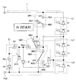
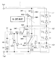
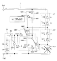
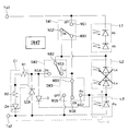
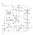
- FIGS. 4 to 15 are circuit diagrams showing an example of operation during normal operation in which the LED lamp of the lamp lighting device 100 according to the first embodiment shown in FIG.
- the first switch circuit SW1 is electrically connected between the first reference node NB1 and the first contact NS1. Further, the second switch circuit SW2 conducts between the second reference node NB2 and the third contact NS3. The third switch circuit SW3 is electrically connected between the third reference node NB3 and the fifth contact NS5.
- the user switches the first switch circuit SW1 to turn off the passing, the second switch circuit SW2 to switch the low beam lamp Lo, and the third switch to turn off the lighting.
- the switch circuit SW3 is switched.
- the first switch circuit SW1 is electrically connected between the first reference node NB1 and the second contact NS2. Further, the second switch circuit SW2 conducts between the second reference node NB2 and the third contact NS3. The third switch circuit SW3 is electrically connected between the third reference node NB3 and the fifth contact NS5.
- the user switches the first switch circuit SW1 to turn on the passing, the second switch circuit SW2 to switch the low beam lamp Lo, and the third switch to turn off the lighting.
- the switch circuit SW3 is switched.
- the first switch circuit SW1 is electrically connected between the first reference node NB1 and the first contact NS1. Further, the second switch circuit SW2 conducts between the second reference node NB2 and the fourth contact NS4. The third switch circuit SW3 is electrically connected between the third reference node NB3 and the fifth contact NS5.
- the first switch circuit SW1 is switched by the user to turn off the passing, the second switch circuit SW2 is switched so that the high beam lamp Hi is selected, and the third switch is turned off to turn off the lighting.
- the switch circuit SW3 is switched.
- the first switch circuit SW1 is electrically connected between the first reference node NB1 and the second contact NS2. Further, the second switch circuit SW2 conducts between the second reference node NB2 and the fourth contact NS4. The third switch circuit SW3 is electrically connected between the third reference node NB3 and the fifth contact NS5.
- the user switches the first switch circuit SW1 to turn on the passing, the second switch circuit SW2 to switch the high beam lamp Hi, and the third switch to turn off the lighting.
- the switch circuit SW3 is switched.
- the first switch circuit SW1 is electrically connected between the first reference node NB1 and the first contact NS1. Further, the second switch circuit SW2 conducts between the second reference node NB2 and the third contact NS3. The third switch circuit SW3 conducts between the third reference node NB3 and the seventh contact NS7.
- the user switches the first switch circuit SW1 so as to turn off the passing, the second switch circuit SW2 is switched so that the low beam lamp Lo is selected, and the position lamp Po is turned on.
- the third switch circuit SW3 is switched.
- the first switch circuit SW1 is electrically connected between the first reference node NB1 and the second contact NS2. Further, the second switch circuit SW2 conducts between the second reference node NB2 and the third contact NS3. The third switch circuit SW3 conducts between the third reference node NB3 and the seventh contact NS7.
- the user switches the first switch circuit SW1 so as to turn on the passing, the second switch circuit SW2 is switched so that the low beam lamp Lo is selected, and the position lamp Po is turned on.
- the third switch circuit SW3 is switched.
- the first switch circuit SW1 is electrically connected between the first reference node NB1 and the first contact NS1. Further, the second switch circuit SW2 conducts between the second reference node NB2 and the fourth contact NS4. The third switch circuit SW3 conducts between the third reference node NB3 and the seventh contact NS7.
- the first switch circuit SW1 is switched by the user so as to turn off the passing, the second switch circuit SW2 is switched so that the high beam lamp Hi is selected, and the position lamp Po is turned on.
- the third switch circuit SW3 is switched.
- the first switch circuit SW1 is electrically connected between the first reference node NB1 and the second contact NS2. Further, the second switch circuit SW2 conducts between the second reference node NB2 and the fourth contact NS4. The third switch circuit SW3 conducts between the third reference node NB3 and the seventh contact NS7.
- the user switches the first switch circuit SW1 so as to turn on the passing, the second switch circuit SW2 is switched so that the high beam lamp Hi is selected, and the position lamp Po is turned on.
- the third switch circuit SW3 is switched.
- the first switch circuit SW1 is electrically connected between the first reference node NB1 and the first contact NS1. Further, the second switch circuit SW2 conducts between the second reference node NB2 and the third contact NS3. The third switch circuit SW3 conducts between the third reference node NB3 and the sixth contact NS6.
- the first switch circuit SW1 is switched by the user to turn off the passing, the second switch circuit SW2 is switched so that the low beam lamp Lo is selected, and the third switch is turned on to turn on the lighting.
- the switch circuit SW3 is switched.
- the first switch circuit SW1 is electrically connected between the first reference node NB1 and the second contact NS2. Further, the second switch circuit SW2 conducts between the second reference node NB2 and the third contact NS3. The third switch circuit SW3 conducts between the third reference node NB3 and the sixth contact NS6.
- the user switches the first switch circuit SW1 to turn on the passing, the second switch circuit SW2 to switch the low beam lamp Lo, and the third switch to turn on the lighting.
- the switch circuit SW3 is switched.
- the first switch circuit SW1 is electrically connected between the first reference node NB1 and the first contact NS1. Further, the second switch circuit SW2 conducts between the second reference node NB2 and the fourth contact NS4. The third switch circuit SW3 conducts between the third reference node NB3 and the sixth contact NS6.
- the user switches the first switch circuit SW1 to turn off the passing, the second switch circuit SW2 to switch the high beam lamp Hi, and the third switch to turn on the lighting.
- the switch circuit SW3 is switched.
- the first lamp circuit L1, the second lamp circuit L2, and the first 3 lamp circuit L3 is extinguished (for example, the state of FIG. 6 with lighting turned OFF).
- the third switch circuit SW3 is switched to turn the lighting from OFF (for example, the state of FIG. 6) to ON (for example, the state of FIG. 14).
- a current is supplied to the first ramp circuit L1, the second ramp circuit L2, and the third ramp circuit L3 from a state where the first external terminal Ta1 and the second external terminal Ta2 are short-circuited. Flows, and the potential difference between the first external terminal Ta1 and the second external terminal Ta2 gradually increases. Thereby, the rush current when the lighting is switched from OFF to ON can be suppressed.
- the first switch circuit SW1 is electrically connected between the first reference node NB1 and the second contact NS2. Further, the second switch circuit SW2 conducts between the second reference node NB2 and the fourth contact NS4. The third switch circuit SW3 conducts between the third reference node NB3 and the sixth contact NS6.
- the user switches the first switch circuit SW1 so as to turn on the passing, the second switch circuit SW2 is switched so that the high beam lamp Hi is selected, and the third switch so as to turn on the lighting.
- the switch circuit SW3 is switched.
- the switch control circuit C1 does not operate, and the switch control circuit C1 does not affect the current i.
- the operation (FIG. 3) in the normal operation in which the LED lamp of the lamp lighting device 100 according to the first embodiment has not failed is the lighting state when the high beam lamp Hi is selected and the lighting is turned on. Except for the difference, the operation is the same as that of the general bulb lamp lighting device shown in FIG.
- FIG. 16 is a diagram showing a relationship between on / off of each switch of a general bulb lamp lighting device and lighting of each bulb lamp when the position lamp Po is out of order.
- FIG. 17 is a diagram showing a relationship between on / off of each switch of the lamp lighting device 100 according to the first embodiment shown in FIG. 1 and lighting of each LED lamp when the position lamp Po is out of order. is there.
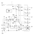
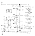
- FIGS. 18 to 29 are circuit diagrams showing an example of the operation when the position lamp Po of the lamp lighting device 100 according to the first embodiment shown in FIG. 1 is out of order.
- the states of the first to third switch circuits SW1 to SW3 are the same as the state shown in FIG.
- the user switches the first switch circuit SW1 to turn off the passing, the second switch circuit SW2 to switch the low beam lamp Lo, and the third switch to turn off the lighting.
- the switch circuit SW3 is switched.
- the user switches the first switch circuit SW1 to turn on the passing, the second switch circuit SW2 to switch the low beam lamp Lo, and the third switch to turn off the lighting.
- the switch circuit SW3 is switched.
- the first switch circuit SW1 is switched by the user to turn off the passing, the second switch circuit SW2 is switched so that the high beam lamp Hi is selected, and the third switch is turned off to turn off the lighting.
- the switch circuit SW3 is switched.
- the user switches the first switch circuit SW1 to turn on the passing, the second switch circuit SW2 to switch the high beam lamp Hi, and the third switch to turn off the lighting.
- the switch circuit SW3 is switched.
- the switch control circuit C1 does not operate and the switch control circuit C1 does not affect the current i.
- the user switches the first switch circuit SW1 so as to turn off the passing, the second switch circuit SW2 is switched so that the low beam lamp Lo is selected, and the position lamp Po is turned on.
- the third switch circuit SW3 is switched.
- the lamp drive power supply 10 is preset with an output voltage to be output between the first power supply terminal TS1 and the second power supply terminal TS2 by the constant voltage control function.
- the voltage is raised to a specified voltage and limited to a certain voltage.
- the user switches the first switch circuit SW1 so as to turn on the passing, the second switch circuit SW2 is switched so that the low beam lamp Lo is selected, and the position lamp Po is turned on.
- the third switch circuit SW3 is switched.
- the switch control circuit C1 turns on the switch element SCR according to the operation principle described with reference to FIG.
- the first switch circuit SW1 is switched by the user so as to turn off the passing, the second switch circuit SW2 is switched so that the high beam lamp Hi is selected, and the position lamp Po is turned on.
- the third switch circuit SW3 is switched.
- the switch control circuit C1 turns on the switch element SCR according to the operation principle described with reference to FIG.
- the user switches the first switch circuit SW1 so as to turn on the passing, the second switch circuit SW2 is switched so that the high beam lamp Hi is selected, and the position lamp Po is turned on.
- the third switch circuit SW3 is switched.
- the switch control circuit C1 turns on the switch element SCR according to the operation principle described with reference to FIG.
- the first switch circuit SW1 is switched by the user to turn off the passing, the second switch circuit SW2 is switched so that the low beam lamp Lo is selected, and the third switch is turned on to turn on the lighting.
- the switch circuit SW3 is switched.
- the switch control circuit C1 turns on the switch element SCR according to the operation principle described with reference to FIG.
- the user switches the first switch circuit SW1 to turn on the passing, the second switch circuit SW2 to switch the low beam lamp Lo, and the third switch to turn on the lighting.
- the switch circuit SW3 is switched.
- the switch control circuit C1 turns on the switch element SCR according to the operation principle described with reference to FIG.
- the user switches the first switch circuit SW1 to turn off the passing, the second switch circuit SW2 to switch the high beam lamp Hi, and the third switch to turn on the lighting.
- the switch circuit SW3 is switched.
- the switch control circuit C1 turns on the switch element SCR according to the operation principle described with reference to FIG.
- the user switches the first switch circuit SW1 so as to turn on the passing, the second switch circuit SW2 is switched so that the high beam lamp Hi is selected, and the third switch so as to turn on the lighting.
- the switch circuit SW3 is switched.
- the switch control circuit C1 turns on the switch element SCR according to the operation principle described with reference to FIG.
- FIG. 30 is a diagram showing a relationship between ON / OFF of each switch of a general bulb lamp lighting device and lighting of each bulb lamp when the low beam lamp Lo is out of order.
- FIG. 31 is a diagram showing a relationship between on / off of each switch of the lamp lighting device 100 according to the first embodiment shown in FIG. 1 and lighting of each LED lamp when the low beam lamp Lo is out of order. It is.
- FIGS. 32 to 43 are circuit diagrams showing an example of the operation when the low beam lamp Lo of the lamp lighting device 100 according to the first embodiment shown in FIG. 1 is out of order.
- the states of the first to third switch circuits SW1 to SW3 are the same as the state shown in FIG. 32.
- the user switches the first switch circuit SW1 to turn off the passing, the second switch circuit SW2 to switch the low beam lamp Lo, and the third switch to turn off the lighting.
- the switch circuit SW3 is switched.
- the user switches the first switch circuit SW1 to turn on the passing, the second switch circuit SW2 to switch the low beam lamp Lo, and the third switch to turn off the lighting.
- the switch circuit SW3 is switched.
- the first switch circuit SW1 is switched by the user to turn off the passing, the second switch circuit SW2 is switched so that the high beam lamp Hi is selected, and the third switch is turned off to turn off the lighting.
- the switch circuit SW3 is switched.
- the user switches the first switch circuit SW1 to turn on the passing, the second switch circuit SW2 to switch the high beam lamp Hi, and the third switch to turn off the lighting.
- the switch circuit SW3 is switched.
- the user switches the first switch circuit SW1 so as to turn off the passing, the second switch circuit SW2 is switched so that the low beam lamp Lo is selected, and the position lamp Po is turned on.
- the third switch circuit SW3 is switched.
- the user switches the first switch circuit SW1 so as to turn on the passing, the second switch circuit SW2 is switched so that the low beam lamp Lo is selected, and the position lamp Po is turned on.
- the third switch circuit SW3 is switched.
- the user switches the first switch circuit SW1 so as to turn off the passing, the second switch circuit SW2 is switched so that the high beam lamp Hi is selected, and the position lamp Po is turned on.
- the third switch circuit SW3 is switched.
- the user switches the first switch circuit SW1 so as to turn on the passing, the second switch circuit SW2 is switched so that the high beam lamp Hi is selected, and the position lamp Po is turned on.
- the third switch circuit SW3 is switched.
- the first switch circuit SW1 is switched by the user to turn off the passing, the second switch circuit SW2 is switched so that the low beam lamp Lo is selected, and the third switch is turned on to turn on the lighting.
- the switch circuit SW3 is switched.
- the user switches the first switch circuit SW1 to turn on the passing, the second switch circuit SW2 to switch the low beam lamp Lo, and the third switch to turn on the lighting.
- the switch circuit SW3 is switched.
- the switch control circuit C1 does not operate, and the switch control circuit C1 does not affect the current i.
- the user switches the first switch circuit SW1 to turn off the passing, the second switch circuit SW2 to switch the high beam lamp Hi, and the third switch to turn on the lighting.
- the switch circuit SW3 is switched.
- the lamp drive power supply 10 is preset with an output voltage to be output between the first power supply terminal TS1 and the second power supply terminal TS2 by the constant voltage control function.
- the voltage is raised to a specified voltage and limited to a certain voltage.
- the user switches the first switch circuit SW1 to turn on the passing, the second switch circuit SW2 to switch the high beam lamp Hi, and the third switch to turn on the lighting.
- the switch circuit SW3 is switched.
- the switch control circuit C1 turns on the switch element SCR according to the operation principle described with reference to FIG.
- the operation when the low beam lamp Lo of the lamp lighting device 100 according to the first embodiment is out of order is the lighting state when the low beam lamp Lo is selected and lighting is turned on. Except for the difference, the operation is the same as when the low-beam lamp Lo of the general bulb lamp lighting device shown in FIG. 30 is out of order.
- FIG. 44 is a diagram showing a relationship between on / off of each switch of a general bulb lamp lighting device and lighting of each bulb lamp when the high beam lamp Hi is out of order.
- FIG. 45 is a diagram showing a relationship between on / off of each switch of the lamp lighting device 100 according to the first embodiment shown in FIG. 1 and lighting of each LED lamp when the high beam lamp Hi is out of order.
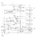
- It is. 46 to 57 are circuit diagrams showing an example of the operation when the high beam lamp Hi of the lamp lighting device 100 according to the first embodiment shown in FIG. 1 is out of order.
- the states of the first to third switch circuits SW1 to SW3 are the same as the state shown in FIG.
- the user switches the first switch circuit SW1 to turn off the passing, the second switch circuit SW2 to switch the low beam lamp Lo, and the third switch to turn off the lighting.
- the switch circuit SW3 is switched.
- the user switches the first switch circuit SW1 to turn on the passing, the second switch circuit SW2 to switch the low beam lamp Lo, and the third switch to turn off the lighting.
- the switch circuit SW3 is switched.
- the first switch circuit SW1 is switched by the user to turn off the passing, the second switch circuit SW2 is switched so that the high beam lamp Hi is selected, and the third switch is turned off to turn off the lighting.
- the switch circuit SW3 is switched.
- the user switches the first switch circuit SW1 to turn on the passing, the second switch circuit SW2 to switch the high beam lamp Hi, and the third switch to turn off the lighting.
- the switch circuit SW3 is switched.
- the user switches the first switch circuit SW1 so as to turn off the passing, the second switch circuit SW2 is switched so that the low beam lamp Lo is selected, and the position lamp Po is turned on.
- the third switch circuit SW3 is switched.
- the user switches the first switch circuit SW1 so as to turn on the passing, the second switch circuit SW2 is switched so that the low beam lamp Lo is selected, and the position lamp Po is turned on.
- the third switch circuit SW3 is switched.
- the first switch circuit SW1 is switched by the user so as to turn off the passing, the second switch circuit SW2 is switched so that the high beam lamp Hi is selected, and the position lamp Po is turned on.
- the third switch circuit SW3 is switched.
- the user switches the first switch circuit SW1 so as to turn on the passing, the second switch circuit SW2 is switched so that the high beam lamp Hi is selected, and the position lamp Po is turned on.
- the third switch circuit SW3 is switched.
- the first switch circuit SW1 is switched by the user to turn off the passing, the second switch circuit SW2 is switched so that the low beam lamp Lo is selected, and the third switch is turned on to turn on the lighting.
- the switch circuit SW3 is switched.
- the user switches the first switch circuit SW1 to turn on the passing, the second switch circuit SW2 to switch the low beam lamp Lo, and the third switch to turn on the lighting.
- the switch circuit SW3 is switched.
- the user switches the first switch circuit SW1 to turn off the passing, the second switch circuit SW2 to switch the high beam lamp Hi, and the third switch to turn on the lighting.
- the switch circuit SW3 is switched.
- the user switches the first switch circuit SW1 so as to turn on the passing, the second switch circuit SW2 is switched so that the high beam lamp Hi is selected, and the third switch so as to turn on the lighting.
- the switch circuit SW3 is switched.
- the switch control circuit C1 does not operate, and the switch control circuit C1 does not affect the current i.
- the operation (FIG. 45) in the case where the high beam lamp Hi of the lamp lighting device 100 according to the first embodiment is out of order is turned on when the high beam lamp Hi is selected and the position lamp Po is turned on. Except for a part of the state being different, the operation is the same as when the high beam lamp Hi of the general bulb lamp lighting device shown in FIG. 44 is out of order.
- the user can control the lighting of each LED lamp by operating each switch circuit.
- the operation of the high beam lamp Hi / low beam lamp Lo is less affected at the time of failure.
- the first external terminal Ta1 and the second external terminal Ta2 are short-circuited, whereby the first lamp circuit L1 and the second lamp circuit. L2 and the third lamp circuit L3 are turned off. Then, for example, the first lamp is switched from the state in which the first external terminal Ta1 and the second external terminal Ta2 are short-circuited by switching the third switch circuit SW3 to turn the lighting from OFF to ON.
- a current flows through the circuit L1, the second ramp circuit L2, and the third ramp circuit L3, and the potential difference between the first external terminal Ta1 and the second external terminal Ta2 gradually increases. Thereby, the rush current when the lighting is switched from OFF to ON can also be suppressed.
- Lamp drive power supply 100 LED lamp lighting device Ta1 First external terminal Ta2 Second external terminal L1 First lamp circuit L2 Second lamp circuit L3 Third lamp circuit SW1 First switch circuit SW2 Second switch circuit SW3 Third switch circuit SCR Switch element D Diode C1 Switch control circuit
Landscapes
- Lighting Device Outwards From Vehicle And Optical Signal (AREA)
- Circuit Arrangement For Electric Light Sources In General (AREA)
Abstract
LEDランプ点灯装置100は、ランプ駆動電源10の低電位側の第1の電源端子TS1と高電位側の第2の電源端子TS2との間に接続され、ランプ駆動電源10から駆動電流の供給を受け、この駆動電流により直列に接続された複数のLEDランプを点灯する。
Description
本発明は、LEDランプ点灯装置、および、LEDランプ点灯装置の制御方法に関する。
一般に、LED (Light Emitting Diode) ランプは、低電圧で駆動することができ、フィラメント灯(バルブランプ)などと比較して長寿命、低消費電力、素早い反応速度、及び耐衝撃性を有しており、小型、軽量化を図ることができる。
このため、LEDランプは、例えば、車両のヘッドランプなどに好適に用いることができる。
このような、LEDランプの駆動装置の一例として、例えば、特開2012-160413号公報に示すようなLED点灯制御装置がある。
この特開2012-160413号公報に記載のLED点灯制御装置は、簡単な回路構成でLEDオープンエラーを検知し、LEDオープンエラーを生じないLED電圧を決定することができる。
しかし、上述した特開2012-160413号公報のLED点灯制御装置のように、直列に接続された複数のLED ランプを1つのドライバ回路で駆動する場合、何れか1灯のLEDランプが破壊(断線) すると全てのLEDランプが消灯するという問題がある。そして、上述した特開2012-160413号公報のLED点灯制御装置は、従来の一般的なバルブランプ点灯装置と同様の動作ができない。
本発明の一態様に係る実施例に従ったLEDランプ点灯装置は、
ランプ駆動電源の低電位側の第1の電源端子と高電位側の第2の電源端子との間に接続され、前記ランプ駆動電源から駆動電流の供給を受け、前記駆動電流により直列に接続された複数のLEDランプを点灯するLEDランプ点灯装置であって、
前記第1の電源端子に接続される第1の外部端子と、
前記第2の電源端子に接続される第2の外部端子と、
1つのLEDランプ又は直列に接続された複数のLEDランプで構成され、一端が前記第1の外部端子に接続された第1のランプ回路と、
1つのLEDランプ又は直列に接続された複数のLEDランプで構成され、一端が前記第1のランプ回路の他端に接続された第2のランプ回路と、
1つのLEDランプ又は直列に接続された複数のLEDランプで構成され、一端が前記第2のランプ回路の他端に接続され、他端が前記第2の外部端子に接続された第3のランプ回路と、
第1の基準ノードと、前記第1の外部端子に接続された第1の接点との間、又は、前記第1の基準ノードと、前記第1のランプ回路の他端に接続された第2の接点との間の何れか一つのみを導通する第1のスイッチ回路と、
前記第1のランプ回路の他端に接続された第2の基準ノードと、前記第1の基準ノードに接続された第3の接点との間、又は、前記第2の基準ノードと第4の接点との間の何れか一つのみを導通する第2のスイッチ回路と、
前記第1の基準ノードに接続された第3の基準ノードと、前記第2の外部端子に接続された第5の接点との間、前記第3の基準ノードと、第6の接点との間、又は、前記第3の基準ノードと、前記第2のランプ回路の他端に接続された第7の接点との間の何れか一つのみを導通する第3のスイッチ回路と、
カソードが第2のランプ回路の他端に接続され、アノードが前記第4の接点に接続されたダイオードと、
一端が前記第4の接点に接続され、他端が前記第2の外部端子に接続されたスイッチ素子と、
前記第4の接点と前記第2の外部端子との間の電位差に応じて、前記スイッチ素子を制御するスイッチ制御回路と、を備え、
前記スイッチ制御回路は、
前記第4の接点と前記第2の外部端子との間の電位差の大きさが、予め設定された基準電圧以上の場合には、前記スイッチ素子をオンし、
前記第4の接点と前記第2の外部端子との間の電位差の大きさが、前記基準電圧未満の場合には、前記スイッチ素子をオフする
ことを特徴とする。
ランプ駆動電源の低電位側の第1の電源端子と高電位側の第2の電源端子との間に接続され、前記ランプ駆動電源から駆動電流の供給を受け、前記駆動電流により直列に接続された複数のLEDランプを点灯するLEDランプ点灯装置であって、
前記第1の電源端子に接続される第1の外部端子と、
前記第2の電源端子に接続される第2の外部端子と、
1つのLEDランプ又は直列に接続された複数のLEDランプで構成され、一端が前記第1の外部端子に接続された第1のランプ回路と、
1つのLEDランプ又は直列に接続された複数のLEDランプで構成され、一端が前記第1のランプ回路の他端に接続された第2のランプ回路と、
1つのLEDランプ又は直列に接続された複数のLEDランプで構成され、一端が前記第2のランプ回路の他端に接続され、他端が前記第2の外部端子に接続された第3のランプ回路と、
第1の基準ノードと、前記第1の外部端子に接続された第1の接点との間、又は、前記第1の基準ノードと、前記第1のランプ回路の他端に接続された第2の接点との間の何れか一つのみを導通する第1のスイッチ回路と、
前記第1のランプ回路の他端に接続された第2の基準ノードと、前記第1の基準ノードに接続された第3の接点との間、又は、前記第2の基準ノードと第4の接点との間の何れか一つのみを導通する第2のスイッチ回路と、
前記第1の基準ノードに接続された第3の基準ノードと、前記第2の外部端子に接続された第5の接点との間、前記第3の基準ノードと、第6の接点との間、又は、前記第3の基準ノードと、前記第2のランプ回路の他端に接続された第7の接点との間の何れか一つのみを導通する第3のスイッチ回路と、
カソードが第2のランプ回路の他端に接続され、アノードが前記第4の接点に接続されたダイオードと、
一端が前記第4の接点に接続され、他端が前記第2の外部端子に接続されたスイッチ素子と、
前記第4の接点と前記第2の外部端子との間の電位差に応じて、前記スイッチ素子を制御するスイッチ制御回路と、を備え、
前記スイッチ制御回路は、
前記第4の接点と前記第2の外部端子との間の電位差の大きさが、予め設定された基準電圧以上の場合には、前記スイッチ素子をオンし、
前記第4の接点と前記第2の外部端子との間の電位差の大きさが、前記基準電圧未満の場合には、前記スイッチ素子をオフする
ことを特徴とする。
前記LEDランプ点灯装置において、
前記第1の外部端子と前記第2の外部端子との間が短絡されることにより、前記第1のランプ回路、前記第2のランプ回路、および、前記第3のランプ回路が消灯する
ことを特徴とする。
前記第1の外部端子と前記第2の外部端子との間が短絡されることにより、前記第1のランプ回路、前記第2のランプ回路、および、前記第3のランプ回路が消灯する
ことを特徴とする。
前記LEDランプ点灯装置において、
前記スイッチ素子は、カソードが前記第4の接点に接続され、アノードが前記第2の外部端子に接続されたサイリスタである
ことを特徴とする。
前記スイッチ素子は、カソードが前記第4の接点に接続され、アノードが前記第2の外部端子に接続されたサイリスタである
ことを特徴とする。
前記LEDランプ点灯装置において、
前記スイッチ制御回路は、
一端が前記第4の接点に接続され、他端が前記サイリスタのゲートに接続された第1の抵抗と、
一端が前記第1の抵抗の他端に接続された第2の抵抗と、
アノードが前記第2の抵抗の他端に接続され、カソードが前記第2の外部端子に接続されたツェナーダイオードと、を有する
ことを特徴とする。
前記スイッチ制御回路は、
一端が前記第4の接点に接続され、他端が前記サイリスタのゲートに接続された第1の抵抗と、
一端が前記第1の抵抗の他端に接続された第2の抵抗と、
アノードが前記第2の抵抗の他端に接続され、カソードが前記第2の外部端子に接続されたツェナーダイオードと、を有する
ことを特徴とする。
前記LEDランプ点灯装置において、
前記ランプ駆動電源は、
交流発電機の一端に接続された第1の入力端子と、
前記交流発電機の他端に接続された第2の入力端子と、
一端が前記第1の入力端子に接続され、他端が前記第1の電源端子に接続された電源用スイッチ素子と、
一端が前記電源用スイッチ素子の他端に接続され、他端が前記第2の入力端子に接続されたコンデンサと、
一端が前記第2の入力端子に接続され、他端が前記第2の電源端子に接続された検出抵抗と、
前記検出抵抗に電流が流れる場合には、前記検出抵抗に流れる電流が一定になるように前記電源用スイッチ素子を制御し、一方、前記検出抵抗に電流が流れない場合には、前記第1の電源端子と前記第2の電源端子との間の電圧が予め設定された規定電圧になるように、前記電源用スイッチ素子を制御する駆動制御回路と、を有する
ことを特徴とする。
前記ランプ駆動電源は、
交流発電機の一端に接続された第1の入力端子と、
前記交流発電機の他端に接続された第2の入力端子と、
一端が前記第1の入力端子に接続され、他端が前記第1の電源端子に接続された電源用スイッチ素子と、
一端が前記電源用スイッチ素子の他端に接続され、他端が前記第2の入力端子に接続されたコンデンサと、
一端が前記第2の入力端子に接続され、他端が前記第2の電源端子に接続された検出抵抗と、
前記検出抵抗に電流が流れる場合には、前記検出抵抗に流れる電流が一定になるように前記電源用スイッチ素子を制御し、一方、前記検出抵抗に電流が流れない場合には、前記第1の電源端子と前記第2の電源端子との間の電圧が予め設定された規定電圧になるように、前記電源用スイッチ素子を制御する駆動制御回路と、を有する
ことを特徴とする。
前記LEDランプ点灯装置において、
前記電源用スイッチ素子は、カソードが前記第1の入力端子に接続され、アノードが前記第1の電源端子に接続され、ゲートに前記駆動制御回路から制御信号が入力されるサイリスタである
ことを特徴とする。
前記電源用スイッチ素子は、カソードが前記第1の入力端子に接続され、アノードが前記第1の電源端子に接続され、ゲートに前記駆動制御回路から制御信号が入力されるサイリスタである
ことを特徴とする。
前記LEDランプ点灯装置において、
前記ランプ駆動電源は、
定電圧制御機能と定電流制御機能を有して構成されており、
前記第1のランプ回路、第2のランプ回路、および前記第3のランプ回路中の何れかのLEDランプに電流を流せる場合には、前記定電流制御機能により、前記LEDランプに定電流を流し、
前記第1のランプ回路、第2のランプ回路、および前記第3のランプ回路中の何れのLEDランプにも電流を流せない場合には、前記定電圧制御機能により、前記第1の電源端子と前記第2の電源端子との間に出力する出力電圧を、予め設定された規定電圧まで上昇させて一定の電圧に制限する
ことを特徴とする。
前記ランプ駆動電源は、
定電圧制御機能と定電流制御機能を有して構成されており、
前記第1のランプ回路、第2のランプ回路、および前記第3のランプ回路中の何れかのLEDランプに電流を流せる場合には、前記定電流制御機能により、前記LEDランプに定電流を流し、
前記第1のランプ回路、第2のランプ回路、および前記第3のランプ回路中の何れのLEDランプにも電流を流せない場合には、前記定電圧制御機能により、前記第1の電源端子と前記第2の電源端子との間に出力する出力電圧を、予め設定された規定電圧まで上昇させて一定の電圧に制限する
ことを特徴とする。
前記LEDランプ点灯装置において、
前記第1のランプ回路の前記一端は、前記第1のランプ回路の前記LEDランプのカソード側であり、
前記第1のランプ回路の前記他端は、前記第1のランプ回路の前記LEDランプのアノード側であり、
前記第2のランプ回路の前記一端は、前記第2のランプ回路の前記LEDランプのカソード側であり、
前記第2のランプ回路の前記他端は、前記第2のランプ回路の前記LEDランプのアノード側であり、
前記第3のランプ回路の前記一端は、前記第3のランプ回路の前記LEDランプのカソード側であり、
前記第3のランプ回路の前記他端は、前記第3のランプ回路の前記LEDランプのアノード側である
ことを特徴とする。
前記第1のランプ回路の前記一端は、前記第1のランプ回路の前記LEDランプのカソード側であり、
前記第1のランプ回路の前記他端は、前記第1のランプ回路の前記LEDランプのアノード側であり、
前記第2のランプ回路の前記一端は、前記第2のランプ回路の前記LEDランプのカソード側であり、
前記第2のランプ回路の前記他端は、前記第2のランプ回路の前記LEDランプのアノード側であり、
前記第3のランプ回路の前記一端は、前記第3のランプ回路の前記LEDランプのカソード側であり、
前記第3のランプ回路の前記他端は、前記第3のランプ回路の前記LEDランプのアノード側である
ことを特徴とする。
前記LEDランプ点灯装置において、
前記第1のスイッチ回路、前記第2のスイッチ回路、および、前記第3のスイッチ回路は、使用者により手動で制御されるようになっている
ことを特徴とする。
前記第1のスイッチ回路、前記第2のスイッチ回路、および、前記第3のスイッチ回路は、使用者により手動で制御されるようになっている
ことを特徴とする。
前記LEDランプ点灯装置において、
前記第1のランプ回路のLEDランプは、車両のヘッドランプのハイビーム用ランプであり、
前記第2のランプ回路のLEDランプは、前記ヘッドランプのロービーム用ランプであり、
前記第3のランプ回路のLEDランプは、前記車両のポジションランプであることを特徴とする。
前記第1のランプ回路のLEDランプは、車両のヘッドランプのハイビーム用ランプであり、
前記第2のランプ回路のLEDランプは、前記ヘッドランプのロービーム用ランプであり、
前記第3のランプ回路のLEDランプは、前記車両のポジションランプであることを特徴とする。
本発明の一態様に係るLED ランプ点灯装置の制御方法は、
ランプ駆動電源の低電位側の第1の電源端子と高電位側の第2の電源端子との間に接続され、前記ランプ駆動電源から駆動電流の供給を受け、前記駆動電流により直列に接続された複数のLEDランプを点灯するLEDランプ点灯装置であって、前記第1の電源端子に接続される第1の外部端子と、前記第2の電源端子に接続される第2の外部端子と、1つのLEDランプ又は直列に接続された複数のLEDランプで構成され、一端が前記第1の外部端子に接続された第1のランプ回路と、1つのLEDランプ又は直列に接続された複数のLEDランプで構成され、一端が前記第1のランプ回路の他端に接続された第2のランプ回路と、1つのLEDランプ又は直列に接続された複数のLEDランプで構成され、一端が前記第2のランプ回路の他端に接続され、他端が前記第2の外部端子に接続された第3のランプ回路と、第1の基準ノードと、前記第1の外部端子に接続された第1の接点との間、又は、前記第1の基準ノードと、前記第1のランプ回路の他端に接続された第2の接点との間の何れか一つのみを導通する第1のスイッチ回路と、前記第1のランプ回路の他端に接続された第2の基準ノードと、前記第1の基準ノードに接続された第3の接点との間、又は、前記第2の基準ノードと第4の接点との間の何れか一つのみを導通する第2のスイッチ回路と、前記第1の基準ノードに接続された第3の基準ノードと、前記第2の外部端子に接続された第5の接点との間、前記第3の基準ノードと、第6の接点との間、又は、前記第3の基準ノードと、前記第2のランプ回路の他端に接続された第7の接点との間の何れか一つのみを導通する第3のスイッチ回路と、カソードが第2のランプ回路の他端に接続され、アノードが前記第4の接点に接続されたダイオードと、一端が前記第4の接点に接続され、他端が前記第2の外部端子に接続されたスイッチ素子と、前記第4の接点と前記第2の外部端子との間の電位差に応じて、前記スイッチ素子を制御するスイッチ制御回路と、を備えるLEDランプ点灯装置の制御方法であって、
前記第4の接点と前記第2の外部端子との間の電位差の大きさが、予め設定された基準電圧以上の場合には、前記スイッチ素子をオンし、
前記第4の接点と前記第2の外部端子との間の電位差の大きさが、前記基準電圧未満の場合には、前記スイッチ素子をオフする
ことを特徴とする。
ランプ駆動電源の低電位側の第1の電源端子と高電位側の第2の電源端子との間に接続され、前記ランプ駆動電源から駆動電流の供給を受け、前記駆動電流により直列に接続された複数のLEDランプを点灯するLEDランプ点灯装置であって、前記第1の電源端子に接続される第1の外部端子と、前記第2の電源端子に接続される第2の外部端子と、1つのLEDランプ又は直列に接続された複数のLEDランプで構成され、一端が前記第1の外部端子に接続された第1のランプ回路と、1つのLEDランプ又は直列に接続された複数のLEDランプで構成され、一端が前記第1のランプ回路の他端に接続された第2のランプ回路と、1つのLEDランプ又は直列に接続された複数のLEDランプで構成され、一端が前記第2のランプ回路の他端に接続され、他端が前記第2の外部端子に接続された第3のランプ回路と、第1の基準ノードと、前記第1の外部端子に接続された第1の接点との間、又は、前記第1の基準ノードと、前記第1のランプ回路の他端に接続された第2の接点との間の何れか一つのみを導通する第1のスイッチ回路と、前記第1のランプ回路の他端に接続された第2の基準ノードと、前記第1の基準ノードに接続された第3の接点との間、又は、前記第2の基準ノードと第4の接点との間の何れか一つのみを導通する第2のスイッチ回路と、前記第1の基準ノードに接続された第3の基準ノードと、前記第2の外部端子に接続された第5の接点との間、前記第3の基準ノードと、第6の接点との間、又は、前記第3の基準ノードと、前記第2のランプ回路の他端に接続された第7の接点との間の何れか一つのみを導通する第3のスイッチ回路と、カソードが第2のランプ回路の他端に接続され、アノードが前記第4の接点に接続されたダイオードと、一端が前記第4の接点に接続され、他端が前記第2の外部端子に接続されたスイッチ素子と、前記第4の接点と前記第2の外部端子との間の電位差に応じて、前記スイッチ素子を制御するスイッチ制御回路と、を備えるLEDランプ点灯装置の制御方法であって、
前記第4の接点と前記第2の外部端子との間の電位差の大きさが、予め設定された基準電圧以上の場合には、前記スイッチ素子をオンし、
前記第4の接点と前記第2の外部端子との間の電位差の大きさが、前記基準電圧未満の場合には、前記スイッチ素子をオフする
ことを特徴とする。
本発明の一態様に係るLED ランプ点灯装置は、ランプ駆動電源の低電位側の第1の電源端子と高電位側の第2の電源端子との間に接続され、ランプ駆動電源から駆動電流の供給を受け、駆動電流により直列に接続された複数のLEDランプを点灯する。LEDランプ点灯装置は、第1の電源端子に接続される第1の外部端子と、第2の電源端子に接続される第2の外部端子と、1つのLEDランプ又は直列に接続された複数のLEDランプで構成され、一端が第1の外部端子に接続された第1のランプ回路と、1つのLEDランプ又は直列に接続された複数のLEDランプで構成され、一端が第1のランプ回路の他端に接続された第2のランプ回路と、1つのLEDランプ又は直列に接続された複数のLEDランプで構成され、一端が第2のランプ回路の他端に接続され、他端が第2の外部端子に接続された第3のランプ回路と、第1の基準ノードと、第1の外部端子に接続された第1の接点との間、又は、第1の基準ノードと、第1のランプ回路の他端に接続された第2の接点との間の何れか一つのみを導通する第1のスイッチ回路と、第1のランプ回路の他端に接続された第2の基準ノードと、第1の基準ノードに接続された第3の接点との間、又は、第2の基準ノードと第4の接点との間の何れか一つのみを導通する第2のスイッチ回路と、第1の基準ノードに接続された第3の基準ノードと、第2の外部端子に接続された第5の接点との間、第3の基準ノードと、第6の接点との間、又は、第3の基準ノードと、第2のランプ回路の他端に接続された第7の接点との間の何れか一つのみを導通する第3のスイッチ回路と、カソードが第2のランプ回路の他端に接続され、アノードが第4の接点に接続されたダイオードと、一端が第4の接点に接続され、他端が第2の外部端子に接続されたスイッチ素子と、第4の接点と第2の外部端子との間の電位差に応じて、スイッチ素子を制御するスイッチ制御回路と、を備える。
そして、スイッチ制御回路は、第4の接点と第2の外部端子との間の電位差の大きさが、予め設定された基準電圧以上の場合には、スイッチ素子をオンし、第4の接点と第2の外部端子との間の電位差の大きさが、基準電圧未満の場合には、スイッチ素子をオフする。
これにより、本発明に係るLED ランプ点灯装置は、従来の一般的なバルブランプ点灯装置と同等の動作が可能となる。
以下、本発明に係る各実施例について図面に基づいて説明する。
図1は、本発明の一態様である実施例1に係るLEDランプ点灯装置の構成の一例を示す回路図である。この図1に示す例は、例えば、車両のヘッドランプの例である。
図1に示すように、LEDランプ点灯装置100には、ランプ駆動電源10が接続される。このランプ駆動電源10には、交流発電機Gが接続される。
ここで、交流発電機Gは、単相交流発電機であり、例えば、車両等のエンジンに連動して回転することにより、交流で発電するようになっている。
この交流発電機Gの一端G1は、ランプ駆動電源10の第1の入力端子TI1に接続され、他端G2は接地されている。交流発電機Gは、発電した交流電圧VAをランプ駆動電源10に出力するようになっている。
そして、ランプ駆動電源10の負電圧側(低電位側)の第1の電源端子TS1は、LEDランプ点灯装置100の外部端子Ta1に接続され、ランプ駆動電源10の正電圧側(高電位側)の第2の電源端子TS2は、LEDランプ点灯装置100の外部端子Ta2に接続される。そして、このランプ駆動電源10は、LEDランプの駆動電流をLEDランプ点灯装置100に供給するようになっている。
すなわち、LEDランプ点灯装置100は、ランプ駆動電源10の低電位側の第1の電源端子TS1と高電位側の第2の電源端子TS2との間に接続され、ランプ駆動電源10から駆動電流の供給を受け、該駆動電流により直列に接続された複数のLEDランプを点灯するようになっている。
このLEDランプ点灯装置100は、例えば、図1に示すように、第1の外部端子Ta1と、第2の外部端子Ta2と、第1のランプ回路L1と、第2のランプ回路L2と、第3のランプ回路L3と、第1のスイッチ回路SW1と、第2のスイッチ回路SW2と、第3のスイッチ回路SW3と、スイッチ素子SCRと、ダイオードDと、スイッチ制御回路C1と、を備える。
第1の外部端子Ta1は、第1の電源端子TS1に接続されるようになっている。
第2の外部端子Ta2は、第2の電源端子TS2に接続されるようになっている。
第1のランプ回路L1は、1つのLEDランプ又は直列に接続された複数のLEDランプで構成され、一端が第1の外部端子Ta1に接続されている。図1の例では、第1のランプ回路L1は、2つのLEDランプが直列に接続されて構成されている。
なお、図1に示すように、第1のランプ回路L1の一端は、第1のランプ回路L1のLEDランプのカソード側である。また、第1のランプ回路L1の他端は、第1のランプ回路L1のLEDランプのアノード側である。
この第1のランプ回路L1のLEDランプは、例えば、車両のヘッドランプのハイビーム用ランプ(例えば、走行用前照灯)Hiである。
第2のランプ回路L2は、1つのLEDランプ又は直列に接続された複数のLEDランプで構成され、一端が第1のランプ回路L1の他端に接続されている。図1の例では、第2のランプ回路L2は、2つのLEDランプが直列に接続されて構成されている。
なお、図1に示すように、第2のランプ回路L2の一端は、第2のランプ回路L2のLEDランプのカソード側である。また、第2のランプ回路L2の他端は、第2のランプ回路L2のLEDランプのアノード側である。
この第2のランプ回路L2のLEDランプは、例えば、該ヘッドランプのロービーム用ランプ(例えば、すれ違い用前照灯)Loである。
第3のランプ回路L3は、1つのLEDランプ又は直列に接続された複数のLEDランプで構成され、一端が第2のランプ回路L2の他端に接続され、他端が第2の外部端子Ta2に接続されている。図1の例では、第3のランプ回路L3は、1つのLEDランプで構成されている。
なお、図1に示すように、第3のランプ回路L3の一端は、第3のランプ回路L3のLEDランプのカソード側である。また、第3のランプ回路L3の他端は、第3のランプ回路L3のLEDランプのアノード側である。
この第3のランプ回路L3のLEDランプは、例えば、該車両のポジションランプPoである。
また、第1のスイッチ回路SW1は、第1の基準ノードNB1と、第1の外部端子Ta1に接続された第1の接点NS1との間、又は、第1の基準ノードNB1と、第1のランプ回路L1の他端に接続された第2の接点NS2との間の何れか一つのみを導通するようになっている。
この第1のスイッチ回路SW1は、既述の車両のヘッドランプのハイランプを点灯(パッシング)させるためのスイッチである。
第2のスイッチ回路SW2は、第1のランプ回路L1の他端に接続された第2の基準ノードNB2と、第1の基準ノードNB1に接続された第3の接点NS3との間、又は、第2の基準ノードNB2と第4の接点NS4との間の何れか一つのみを導通するようになっている。
この第2のスイッチ回路SW2は、既述の車両のヘッドランプのハイビームとロービームとを切り替えるためのスイッチである。
第3のスイッチ回路SW3は、第1の基準ノードNB1に接続された第3の基準ノードNB3と、第2の外部端子Ta2に接続された第5の接点NS5との間、第3の基準ノードNB3と、第6の接点NS6との間、又は、第3の基準ノードNB3と、第2のランプ回路L2の他端に接続された第7の接点NS7との間の何れか一つのみを導通するようになっている。
この第3のスイッチ回路SW3は、既述の車両のポジションランプの点灯、各ランプの点灯又は消灯を制御するためのスイッチである。
なお、上記第1のスイッチ回路SW1、第2のスイッチ回路SW2、および、第3のスイッチ回路SW3は、使用者により手動で制御されるようになっている。
また、ダイオードDは、カソードが第2のランプ回路L2の他端に接続され、アノードが第4の接点NS4に接続されている。
スイッチ素子SCRは、一端が第4の接点NS4に接続され、他端が第2の外部端子Ta2に接続されている。このスイッチ素子SCRは、図1に示すように、カソードが第4の接点NS4に接続され、アノードが第2の外部端子Ta2に接続されたサイリスタである。
スイッチ制御回路C1は、第4の接点NS4と第2の外部端子Ta2との間の電位差に応じて、スイッチ素子SCRを制御するようになっている。
例えば、スイッチ制御回路C1は、第4の接点NS4(スイッチ素子SCRの一端(カソード))と第2の外部端子Ta2との間の電位差の大きさ(絶対値)が、予め設定された基準電圧以上の場合には、スイッチ素子SCRをオンするようになっている。なお、該基準電圧は、その値の大きさ(絶対値)で比較される(以下同様)。
一方、スイッチ制御回路C1は、第4の接点NS4(スイッチ素子SCRの一端(カソード))と第2の外部端子Ta2との間の電位差の大きさ(絶対値)が、該基準電圧未満の場合には、スイッチ素子SCRをオフするようになっている。
このスイッチ制御回路C1は、図1に示すように、例えば、第1の抵抗R1と、第2の抵抗R2と、ツェナーダイオードZeと、を有する。
第1の抵抗R1は、一端が第4の接点NS4に接続され、他端がサイリスタ(スイッチ素子)SCRのゲートに接続されている。
第1の抵抗R1は、一端が第4の接点NS4に接続され、他端がサイリスタ(スイッチ素子)SCRのゲートに接続されている。
第2の抵抗R2は、一端が第1の抵抗R1の他端に接続されている。
ツェナーダイオードZeは、アノードが第2の抵抗R2の他端に接続され、カソードが第2の外部端子Ta2に接続されている。
このスイッチ制御回路C1は、第1の抵抗R1と、第2の抵抗R2と、ツェナーダイオードZeとにより、第4の接点NS4の電圧を監視するように構成されている。
つまり、第4の接点と第2の外部端子Ta2との間の電位差(絶対値)が、該基準電圧よりも大きくなった場合に、ツェナーダイオードZeが導通し、第2の抵抗R2に電流が流れるように構成されている。
そして、ツェナーダイオードZeが導通し、第2の抵抗R2に電流が流れることにより、スイッチ素子(サイリスタ)SCRのアノードとゲートとの間に電圧が発生する。この電圧によりスイッチ素子SCRのゲートにゲート電流が流れて、スイッチ素子SCRがターンオンする。
なお、該基準電圧は、第1の抵抗R1と第2の抵抗R2の抵抗値と、ツェナーダイオードZeの降伏電圧により、所望の値に設定することができる。
ここで、既述のランプ駆動電源10は、図1に示すように、例えば、第1の入力端子TI1と、第2の入力端子TI2と、第1の電源端子TS1と、第2の電源端子TS2と、電源用スイッチ素子Xと、コンデンサCXと、検出抵抗RXと、駆動制御回路CONと、を有する。
第1の入力端子TI1は、交流発電機Gの一端G1に接続されている。
第2の入力端子TI2は、交流発電機Gの他端G2に接地を介して接続されている。
電源用スイッチ素子Xは、一端が第1の入力端子TI1に接続され、他端が第1の電源端子TS1に接続されている。
この電源用スイッチ素子Xは、図1に示すように、例えば、カソードが第1の入力端子TI1に接続され、アノードが第1の電源端子TS1に接続され、ゲートに駆動制御回路CONから制御信号が入力されるサイリスタである。
コンデンサCXは、一端が電源用スイッチ素子Xの他端に接続され、他端が第2の入力端子TI2に接続されている。このコンデンサCXは、平滑用コンデンサ(電解コンデンサ)である。
検出抵抗RXは、一端が第2の入力端子TI2に接続され、他端が第2の電源端子TS2に接続されている。
駆動制御回路CONは、検出抵抗RXに電流が流れる場合には、検出抵抗RXに流れる電流が一定になるように電源用スイッチ素子Xを制御するようになっている。
これにより、電源用スイッチ素子(サイリスタ)Xは、交流発電機Gが出力する交流電圧VAの負相側の電圧を、駆動制御回路CONの制御に基づき半波整流し、LEDランプ点灯装置100に駆動電流が供給される。また、電源用スイッチ素子(サイリスタ)Xは、導通期間中にコンデンサCXを充電する。このコンデンサCXは、電源用スイッチ素子(サイリスタ)Xの非導通期間において、LEDランプ点灯装置100に電流を供給するための整流平滑用コンデンサとなる。
すなわち、駆動制御回路CONは、LEDランプ点灯装置100に流れる電流の実効値又は平均値が一定になるように、電源用スイッチ素子(サイリスタ)Xの導通タイミング(点弧位相)を制御する。
一方、駆動制御回路CONは、検出抵抗RXに電流が流れない場合には、第1の電源端子TS1と第2の電源端子TS2との間の電位差が予め設定された規定電圧になるように、電源用スイッチ素子Xを制御するようになっている。
以上のように、ランプ駆動電源10は、定電圧制御機能と定電流制御機能を有して構成されている。
すなわち、ランプ駆動電源10は、第1のランプ回路L1、第2のランプ回路L2、および第3のランプ回路L3中の何れかのLEDランプに電流を流せる場合には、該定電流制御機能により、LEDランプに定電流を流す(第2の電源端子TS2から一定の電流を出力する)。
なお、ここでは、LEDランプに電流を流せる場合とは、LEDランプが故障していない(導通している)場合である。
一方、ランプ駆動電源10は、第1のランプ回路L1、第2のランプ回路L2、および第3のランプ回路L3中の何れのLEDランプにも電流を流せない(故障している)場合には、該定電圧制御機能により、第1の電源端子TS1と第2の電源端子TS2との間に出力する出力電圧を、予め設定された規定電圧まで上昇させて一定の電圧にする。
なお、ここでは、LEDランプに電流を流せない場合とは、LEDランプが故障している(断線している)場合であり、負荷オープン状態である。
ここで、以上のような構成を有するLEDランプ点灯装置100の動作について説明する。
先ず、ランプ点灯装置100のLEDランプが故障していない通常動作時における動作について説明する。
図2は、一般的なバルブランプ点灯装置の各スイッチのオン/オフと、各バルブランプの点灯との関係を示す図である。また、図3は、図1に示す実施例1に係るランプ点灯装置100の各スイッチのオン/オフと、各LEDランプの点灯との関係を示す図である。また、図4から図15は、図1に示す実施例1に係るランプ点灯装置100のLEDランプが故障していない通常動作時における動作の例を示す回路図である。
例えば、図4の例では、第1のスイッチ回路SW1は、第1の基準ノードNB1と第1の接点NS1との間を導通している。また、第2のスイッチ回路SW2は、第2の基準ノードNB2と第3の接点NS3との間を導通している。第3のスイッチ回路SW3は、第3の基準ノードNB3と第5の接点NS5との間を導通している。
すなわち、使用者により、パッシングをOFFするように第1のスイッチ回路SW1が切り替えられ、ロービーム用ランプLoが選択されるように第2のスイッチ回路SW2が切り替えられ、ライティングをOFFするように第3のスイッチ回路SW3が切り替えられている。
これにより、ランプ駆動電源10から供給される電流iが、「第3のスイッチ回路SW3→第1のスイッチ回路SW1」の経路で流れる。すなわち、第1の外部端子Ta1と第2の外部端子Ta2との間が短絡される。これにより、第1から第3のランプ回路L1~L3は消灯する(図3)。
次に、図5の例では、第1のスイッチ回路SW1は、第1の基準ノードNB1と第2の接点NS2との間を導通している。また、第2のスイッチ回路SW2は、第2の基準ノードNB2と第3の接点NS3との間を導通している。第3のスイッチ回路SW3は、第3の基準ノードNB3と第5の接点NS5との間を導通している。
すなわち、使用者により、パッシングをONするように第1のスイッチ回路SW1が切り替えられ、ロービーム用ランプLoが選択されるように第2のスイッチ回路SW2が切り替えられ、ライティングをOFFするように第3のスイッチ回路SW3が切り替えられている。
これにより、ランプ駆動電源10から供給される電流iが、「第3のスイッチ回路SW3→第2のスイッチ回路SW2→第1のランプ回路L1」の経路で流れる。これにより、ハイビーム用ランプHiの合計2灯が点灯する(図3)。
次に、図6の例では、第1のスイッチ回路SW1は、第1の基準ノードNB1と第1の接点NS1との間を導通している。また、第2のスイッチ回路SW2は、第2の基準ノードNB2と第4の接点NS4との間を導通している。第3のスイッチ回路SW3は、第3の基準ノードNB3と第5の接点NS5との間を導通している。
すなわち、使用者により、パッシングをOFFするように第1のスイッチ回路SW1が切り替えられ、ハイビーム用ランプHiが選択されるように第2のスイッチ回路SW2が切り替えられ、ライティングをOFFするように第3のスイッチ回路SW3が切り替えられている。
これにより、ランプ駆動電源10から供給される電流iが、「第3のスイッチ回路SW3→第1のランプ回路L1」の経路で流れる。すなわち、第1の外部端子Ta1と第2の外部端子Ta2との間が短絡される。これにより、第1から第3のランプ回路L1~L3は消灯する(図3)。
次に、図7の例では、第1のスイッチ回路SW1は、第1の基準ノードNB1と第2の接点NS2との間を導通している。また、第2のスイッチ回路SW2は、第2の基準ノードNB2と第4の接点NS4との間を導通している。第3のスイッチ回路SW3は、第3の基準ノードNB3と第5の接点NS5との間を導通している。
すなわち、使用者により、パッシングをONするように第1のスイッチ回路SW1が切り替えられ、ハイビーム用ランプHiが選択されるように第2のスイッチ回路SW2が切り替えられ、ライティングをOFFするように第3のスイッチ回路SW3が切り替えられている。
これにより、ランプ駆動電源10から供給される電流iが、「第3のスイッチ回路SW3→第1のスイッチ回路SW1→第1のランプ回路L1」の経路で流れる。これにより、ハイビーム用ランプHiの合計2灯が点灯する(図3)。
次に、図8の例では、第1のスイッチ回路SW1は、第1の基準ノードNB1と第1の接点NS1との間を導通している。また、第2のスイッチ回路SW2は、第2の基準ノードNB2と第3の接点NS3との間を導通している。第3のスイッチ回路SW3は、第3の基準ノードNB3と第7の接点NS7との間を導通している。
すなわち、使用者により、パッシングをOFFするように第1のスイッチ回路SW1が切り替えられ、ロービーム用ランプLoが選択されるように第2のスイッチ回路SW2が切り替えられ、ポジションランプPoが点灯するように第3のスイッチ回路SW3が切り替えられている。
これにより、ランプ駆動電源10から供給される電流iが、「第3のランプ回路L3→第3のスイッチ回路SW3→第1のスイッチ回路SW1」の経路で流れる。これにより、ポジションランプPoの合計1灯が点灯する(図3)。
次に、図9の例では、第1のスイッチ回路SW1は、第1の基準ノードNB1と第2の接点NS2との間を導通している。また、第2のスイッチ回路SW2は、第2の基準ノードNB2と第3の接点NS3との間を導通している。第3のスイッチ回路SW3は、第3の基準ノードNB3と第7の接点NS7との間を導通している。
すなわち、使用者により、パッシングをONするように第1のスイッチ回路SW1が切り替えられ、ロービーム用ランプLoが選択されるように第2のスイッチ回路SW2が切り替えられ、ポジションランプPoが点灯するように第3のスイッチ回路SW3が切り替えられている。
これにより、ランプ駆動電源10から供給される電流iが、「第3のランプ回路L3→第3のスイッチ回路SW3→第2のスイッチ回路SW2→第1のランプ回路L1」の経路で流れる。これにより、ハイビーム用ランプHiおよびポジションランプPoの合計3灯が点灯する(図3)。
次に、図10の例では、第1のスイッチ回路SW1は、第1の基準ノードNB1と第1の接点NS1との間を導通している。また、第2のスイッチ回路SW2は、第2の基準ノードNB2と第4の接点NS4との間を導通している。第3のスイッチ回路SW3は、第3の基準ノードNB3と第7の接点NS7との間を導通している。
すなわち、使用者により、パッシングをOFFするように第1のスイッチ回路SW1が切り替えられ、ハイビーム用ランプHiが選択されるように第2のスイッチ回路SW2が切り替えられ、ポジションランプPoが点灯するように第3のスイッチ回路SW3が切り替えられている。
これにより、ランプ駆動電源10から供給される電流iが、「第3のランプ回路L3→第3のスイッチ回路SW3→第1のランプ回路L1」の経路で流れる。これにより、ポジションランプPoの合計1灯が点灯する(図3)。
次に、図11の例では、第1のスイッチ回路SW1は、第1の基準ノードNB1と第2の接点NS2との間を導通している。また、第2のスイッチ回路SW2は、第2の基準ノードNB2と第4の接点NS4との間を導通している。第3のスイッチ回路SW3は、第3の基準ノードNB3と第7の接点NS7との間を導通している。
すなわち、使用者により、パッシングをONするように第1のスイッチ回路SW1が切り替えられ、ハイビーム用ランプHiが選択されるように第2のスイッチ回路SW2が切り替えられ、ポジションランプPoが点灯するように第3のスイッチ回路SW3が切り替えられている。
これにより、ランプ駆動電源10から供給される電流iが、「第3のランプ回路L3→第3のスイッチ回路SW3→第1のスイッチ回路SW1→第1のランプ回路L1」の経路で流れる。これにより、ハイビーム用ランプHiおよびポジションランプPoの合計3灯が点灯する(図3)。
次に、図12の例では、第1のスイッチ回路SW1は、第1の基準ノードNB1と第1の接点NS1との間を導通している。また、第2のスイッチ回路SW2は、第2の基準ノードNB2と第3の接点NS3との間を導通している。第3のスイッチ回路SW3は、第3の基準ノードNB3と第6の接点NS6との間を導通している。
すなわち、使用者により、パッシングをOFFするように第1のスイッチ回路SW1が切り替えられ、ロービーム用ランプLoが選択されるように第2のスイッチ回路SW2が切り替えられ、ライティングをONするように第3のスイッチ回路SW3が切り替えられている。
これにより、ランプ駆動電源10から供給される電流iが、「第3のランプ回路L3→第2のランプ回路L2→第2のスイッチ回路SW2→第1のスイッチ回路SW1」の経路で流れる。これにより、ロービーム用ランプLoおよびポジションランプPoの合計3灯が点灯する(図3)。
次に、図13の例では、第1のスイッチ回路SW1は、第1の基準ノードNB1と第2の接点NS2との間を導通している。また、第2のスイッチ回路SW2は、第2の基準ノードNB2と第3の接点NS3との間を導通している。第3のスイッチ回路SW3は、第3の基準ノードNB3と第6の接点NS6との間を導通している。
すなわち、使用者により、パッシングをONするように第1のスイッチ回路SW1が切り替えられ、ロービーム用ランプLoが選択されるように第2のスイッチ回路SW2が切り替えられ、ライティングをONするように第3のスイッチ回路SW3が切り替えられている。
これにより、ランプ駆動電源10から供給される電流iが、「第3のランプ回路L3→第2のランプ回路L2→第1のランプ回路L1」の経路で流れる。これにより、ハイビーム用ランプHi、ロービーム用ランプLoおよびポジションランプPoの全灯が点灯する(図3)。
次に、図14の例では、第1のスイッチ回路SW1は、第1の基準ノードNB1と第1の接点NS1との間を導通している。また、第2のスイッチ回路SW2は、第2の基準ノードNB2と第4の接点NS4との間を導通している。第3のスイッチ回路SW3は、第3の基準ノードNB3と第6の接点NS6との間を導通している。
すなわち、使用者により、パッシングをOFFするように第1のスイッチ回路SW1が切り替えられ、ハイビーム用ランプHiが選択されるように第2のスイッチ回路SW2が切り替えられ、ライティングをONするように第3のスイッチ回路SW3が切り替えられている。
これにより、ランプ駆動電源10から供給される電流iが、「第3のランプ回路L3→第2のランプ回路L2→第1のランプ回路L1」の経路で流れる。これにより、ハイビーム用ランプHi、ロービーム用ランプLoおよびポジションランプPoの全灯が点灯する(図3)。
ここで、LEDランプ点灯装置100において、第1の外部端子Ta1と第2の外部端子Ta2との間が短絡されることにより、第1のランプ回路L1、第2のランプ回路L2、および、第3のランプ回路L3が消灯する(例えば、ライティングをOFFした図6の状態)。そして、例えば、第3のスイッチ回路SW3を切り替えてライティングをOFF(例えば、図6の状態)からON(例えば、図14の状態)にする。この場合、第1の外部端子Ta1と第2の外部端子Ta2との間が短絡された状態から、第1のランプ回路L1、第2のランプ回路L2、および、第3のランプ回路L3に電流が流れて、第1の外部端子Ta1と第2の外部端子Ta2との間の電位差が徐々に大きくなる。これにより、ライティングをOFFからONにした場合のラッシュ電流を抑制できる。
次に、図15の例では、第1のスイッチ回路SW1は、第1の基準ノードNB1と第2の接点NS2との間を導通している。また、第2のスイッチ回路SW2は、第2の基準ノードNB2と第4の接点NS4との間を導通している。第3のスイッチ回路SW3は、第3の基準ノードNB3と第6の接点NS6との間を導通している。
すなわち、使用者により、パッシングをONするように第1のスイッチ回路SW1が切り替えられ、ハイビーム用ランプHiが選択されるように第2のスイッチ回路SW2が切り替えられ、ライティングをONするように第3のスイッチ回路SW3が切り替えられている。
これにより、ランプ駆動電源10から供給される電流iが、「第3のランプ回路L3→第2のランプ回路L2→第1のランプ回路L1」の経路で流れる。これにより、ハイビーム用ランプHi、ロービーム用ランプLoおよびポジションランプPoの全灯が点灯する(図3)。
なお、上記図4から図15に示す通常動作時の場合においては、スイッチ制御回路C1は動作せず、このスイッチ制御回路C1が、電流iに影響を与えることはない。
以上のように、実施例1に係るランプ点灯装置100のLEDランプが故障していない通常動作時における動作(図3)は、ハイビーム用ランプHiが選択され且つライティングをONする場合の点灯状態が異なる以外は、図2に示す一般的なバルブランプ点灯装置の動作と同等になる。
次に、ランプ点灯装置100のポジションランプPoが故障している場合における動作について説明する。
図16は、一般的なバルブランプ点灯装置の各スイッチのオン/オフと、ポジションランプPoが故障している場合における各バルブランプの点灯との関係を示す図である。また、図17は、図1に示す実施例1に係るランプ点灯装置100の各スイッチのオン/オフと、ポジションランプPoが故障している場合における各LEDランプの点灯との関係を示す図である。また、図18から図29は、図1に示す実施例1に係るランプ点灯装置100のポジションランプPoが故障している場合における動作の例を示す回路図である。
例えば、図18の例では、第1から第3のスイッチ回路SW1~SW3の状態は、既述の図4に示す状態と同様である。
すなわち、使用者により、パッシングをOFFするように第1のスイッチ回路SW1が切り替えられ、ロービーム用ランプLoが選択されるように第2のスイッチ回路SW2が切り替えられ、ライティングをOFFするように第3のスイッチ回路SW3が切り替えられている。
これにより、ランプ駆動電源10から供給される電流iが、「第3のスイッチ回路SW3→第1のスイッチ回路SW1」の経路で流れる。すなわち、第1の外部端子Ta1と第2の外部端子Ta2との間が短絡される。これにより、第1から第3のランプ回路L1~L3は消灯する(図17)。
次に、図19の例では、第1から第3のスイッチ回路SW1~SW3の状態は、既述の図5に示す状態と同様である。
すなわち、使用者により、パッシングをONするように第1のスイッチ回路SW1が切り替えられ、ロービーム用ランプLoが選択されるように第2のスイッチ回路SW2が切り替えられ、ライティングをOFFするように第3のスイッチ回路SW3が切り替えられている。
これにより、ランプ駆動電源10から供給される電流iが、「第3のスイッチ回路SW3→第2のスイッチ回路SW2→第1のランプ回路L1」の経路で流れる。これにより、ハイビーム用ランプHiの合計2灯が点灯する(図17)。
次に、図20の例では、第1から第3のスイッチ回路SW1~SW3の状態は、既述の図6に示す状態と同様である。
すなわち、使用者により、パッシングをOFFするように第1のスイッチ回路SW1が切り替えられ、ハイビーム用ランプHiが選択されるように第2のスイッチ回路SW2が切り替えられ、ライティングをOFFするように第3のスイッチ回路SW3が切り替えられている。
これにより、ランプ駆動電源10から供給される電流iが、「第3のスイッチ回路SW3→第1のランプ回路L1」の経路で流れる。すなわち、第1の外部端子Ta1と第2の外部端子Ta2との間が短絡される。これにより、第1から第3のランプ回路L1~L3は消灯する(図17)。
次に、図21の例では、第1から第3のスイッチ回路SW1~SW3の状態は、既述の図7に示す状態と同様である。
すなわち、使用者により、パッシングをONするように第1のスイッチ回路SW1が切り替えられ、ハイビーム用ランプHiが選択されるように第2のスイッチ回路SW2が切り替えられ、ライティングをOFFするように第3のスイッチ回路SW3が切り替えられている。
これにより、ランプ駆動電源10から供給される電流iが、「第3のスイッチ回路SW3→第1のスイッチ回路SW1→第1のランプ回路L1」の経路で流れる。これにより、ハイビーム用ランプHiの合計2灯が点灯する(図17)。
なお、上記図18から図21に示す場合においては、スイッチ制御回路C1は動作せず、このスイッチ制御回路C1が、電流iに影響を与えることはない。
次に、図22の例では、第1から第3のスイッチ回路SW1~SW3の状態は、既述の図8に示す状態と同様である。
すなわち、使用者により、パッシングをOFFするように第1のスイッチ回路SW1が切り替えられ、ロービーム用ランプLoが選択されるように第2のスイッチ回路SW2が切り替えられ、ポジションランプPoが点灯するように第3のスイッチ回路SW3が切り替えられている。
ここで、上記各スイッチ回路SW1~SW3の状態では、ポジションランプPoが故障しているため、電流iが流れない。しかし、このとき、既述のように、ランプ駆動電源10は、該定電圧制御機能により、第1の電源端子TS1と第2の電源端子TS2との間に出力する出力電圧を、予め設定された規定電圧まで上昇させて一定の電圧に制限する。これにより、第4の接点NS4と第2の外部端子Ta2との間の電位差の大きさが、該基準電圧以上になると、スイッチ制御回路C1は、スイッチ素子SCRをオンする。
これにより、ランプ駆動電源10から供給される電流iが、「スイッチ素子SCR→ダイオードD→第3のスイッチ回路SW3→第1のスイッチ回路SW1」の経路で流れる。すなわち、第1の外部端子Ta1と第2の外部端子Ta2との間が短絡される。これにより、第1から第3のランプ回路L1~L3は消灯する(図17)。
次に、図23の例では、第1から第3のスイッチ回路SW1~SW3の状態は、既述の図9に示す状態と同様である。
すなわち、使用者により、パッシングをONするように第1のスイッチ回路SW1が切り替えられ、ロービーム用ランプLoが選択されるように第2のスイッチ回路SW2が切り替えられ、ポジションランプPoが点灯するように第3のスイッチ回路SW3が切り替えられている。
そして、図22で説明した既述の動作原理により、スイッチ制御回路C1は、スイッチ素子SCRをオンする。
これにより、ランプ駆動電源10から供給される電流iが、「スイッチ素子SCR→ダイオードD→第3のスイッチ回路SW3→第2のスイッチ回路SW2→第1のランプ回路L1」の経路で流れる。これにより、ハイビーム用ランプHiの合計2灯が点灯する(図17)。
次に、図24の例では、第1から第3のスイッチ回路SW1~SW3の状態は、既述の図10に示す状態と同様である。
すなわち、使用者により、パッシングをOFFするように第1のスイッチ回路SW1が切り替えられ、ハイビーム用ランプHiが選択されるように第2のスイッチ回路SW2が切り替えられ、ポジションランプPoが点灯するように第3のスイッチ回路SW3が切り替えられている。
そして、図22で説明した既述の動作原理により、スイッチ制御回路C1は、スイッチ素子SCRをオンする。
これにより、ランプ駆動電源10から供給される電流iが、「スイッチ素子SCR→ダイオードD→第3のスイッチ回路SW3→第1のスイッチ回路SW1」の経路で流れる。すなわち、第1の外部端子Ta1と第2の外部端子Ta2との間が短絡される。これにより、第1から第3のランプ回路L1~L3は消灯する(図17)。
次に、図25の例では、第1から第3のスイッチ回路SW1~SW3の状態は、既述の図11に示す状態と同様である。
すなわち、使用者により、パッシングをONするように第1のスイッチ回路SW1が切り替えられ、ハイビーム用ランプHiが選択されるように第2のスイッチ回路SW2が切り替えられ、ポジションランプPoが点灯するように第3のスイッチ回路SW3が切り替えられている。
そして、図22で説明した既述の動作原理により、スイッチ制御回路C1は、スイッチ素子SCRをオンする。
これにより、ランプ駆動電源10から供給される電流iが、「スイッチ素子SCR→第2のスイッチ回路SW2→第1のランプ回路L1」の経路で流れる。これにより、ハイビーム用ランプHiの合計2灯が点灯する(図17)。
次に、図26の例では、第1から第3のスイッチ回路SW1~SW3の状態は、既述の図12に示す状態と同様である。
すなわち、使用者により、パッシングをOFFするように第1のスイッチ回路SW1が切り替えられ、ロービーム用ランプLoが選択されるように第2のスイッチ回路SW2が切り替えられ、ライティングをONするように第3のスイッチ回路SW3が切り替えられている。
そして、図22で説明した既述の動作原理により、スイッチ制御回路C1は、スイッチ素子SCRをオンする。
これにより、ランプ駆動電源10から供給される電流iが、「スイッチ素子SCR→ダイオードD→第2のランプ回路L2→第2のスイッチ回路SW2→第1のスイッチ回路SW1」の経路で流れる。これにより、ロービーム用ランプLoの合計2灯が点灯する(図17)。
次に、図27の例では、第1から第3のスイッチ回路SW1~SW3の状態は、既述の図13に示す状態と同様である。
すなわち、使用者により、パッシングをONするように第1のスイッチ回路SW1が切り替えられ、ロービーム用ランプLoが選択されるように第2のスイッチ回路SW2が切り替えられ、ライティングをONするように第3のスイッチ回路SW3が切り替えられている。
そして、図22で説明した既述の動作原理により、スイッチ制御回路C1は、スイッチ素子SCRをオンする。
これにより、ランプ駆動電源10から供給される電流iが、「スイッチ素子SCR→ダイオードD→第2のランプ回路L2→第1のランプ回路L1」の経路で流れる。これにより、ハイビーム用ランプHi、およびロービーム用ランプLoの合計4灯が点灯する(図17)。
次に、図28の例では、第1から第3のスイッチ回路SW1~SW3の状態は、既述の図14に示す状態と同様である。
すなわち、使用者により、パッシングをOFFするように第1のスイッチ回路SW1が切り替えられ、ハイビーム用ランプHiが選択されるように第2のスイッチ回路SW2が切り替えられ、ライティングをONするように第3のスイッチ回路SW3が切り替えられている。
そして、図22で説明した既述の動作原理により、スイッチ制御回路C1は、スイッチ素子SCRをオンする。
これにより、ランプ駆動電源10から供給される電流iが、「スイッチ素子SCR→第2のスイッチ回路SW2→第1のランプ回路L1」の経路で流れる。これにより、ハイビーム用ランプHiの合計2灯が点灯する(図17)。
次に、図29の例では、第1から第3のスイッチ回路SW1~SW3の状態は、既述の図15に示す状態と同様である。
すなわち、使用者により、パッシングをONするように第1のスイッチ回路SW1が切り替えられ、ハイビーム用ランプHiが選択されるように第2のスイッチ回路SW2が切り替えられ、ライティングをONするように第3のスイッチ回路SW3が切り替えられている。
そして、図22で説明した既述の動作原理により、スイッチ制御回路C1は、スイッチ素子SCRをオンする。
これにより、ランプ駆動電源10から供給される電流iが、「スイッチ素子SCR→第2のスイッチ回路SW2→第1のランプ回路L1」の経路で流れる。これにより、ハイビーム用ランプHiの合計2灯が点灯する(図17)。
以上のように、実施例1に係るランプ点灯装置100のポジションランプPoが故障している場合における動作(図17)は、図16に示す一般的なバルブランプ点灯装置のポジションランプPoが故障している場合における動作と同等になる。
次に、ランプ点灯装置100のロービーム用ランプLoが故障している場合における動作について説明する。
図30は、一般的なバルブランプ点灯装置の各スイッチのオン/オフと、ロービーム用ランプLoが故障している場合における各バルブランプの点灯との関係を示す図である。また、図31は、図1に示す実施例1に係るランプ点灯装置100の各スイッチのオン/オフと、ロービーム用ランプLoが故障している場合における各LEDランプの点灯との関係を示す図である。また、図32から図43は、図1に示す実施例1に係るランプ点灯装置100のロービーム用ランプLoが故障している場合における動作の例を示す回路図である。
例えば、図32の例では、第1から第3のスイッチ回路SW1~SW3の状態は、既述の図4に示す状態と同様である。
すなわち、使用者により、パッシングをOFFするように第1のスイッチ回路SW1が切り替えられ、ロービーム用ランプLoが選択されるように第2のスイッチ回路SW2が切り替えられ、ライティングをOFFするように第3のスイッチ回路SW3が切り替えられている。
これにより、ランプ駆動電源10から供給される電流iが、「第3のスイッチ回路SW3→第1のスイッチ回路SW1」の経路で流れる。すなわち、第1の外部端子Ta1と第2の外部端子Ta2との間が短絡される。これにより、第1から第3のランプ回路L1~L3は消灯する(図31)。
次に、図33の例では、第1から第3のスイッチ回路SW1~SW3の状態は、既述の図5に示す状態と同様である。
すなわち、使用者により、パッシングをONするように第1のスイッチ回路SW1が切り替えられ、ロービーム用ランプLoが選択されるように第2のスイッチ回路SW2が切り替えられ、ライティングをOFFするように第3のスイッチ回路SW3が切り替えられている。
これにより、ランプ駆動電源10から供給される電流iが、「第3のスイッチ回路SW3→第2のスイッチ回路SW2→第1のランプ回路L1」の経路で流れる。これにより、ハイビーム用ランプHiの合計2灯が点灯する(図31)。
次に、図34の例では、第1から第3のスイッチ回路SW1~SW3の状態は、既述の図6に示す状態と同様である。
すなわち、使用者により、パッシングをOFFするように第1のスイッチ回路SW1が切り替えられ、ハイビーム用ランプHiが選択されるように第2のスイッチ回路SW2が切り替えられ、ライティングをOFFするように第3のスイッチ回路SW3が切り替えられている。
これにより、ランプ駆動電源10から供給される電流iが、「第3のスイッチ回路SW3→第1のスイッチ回路SW1」の経路で流れる。すなわち、第1の外部端子Ta1と第2の外部端子Ta2との間が短絡される。これにより、第1から第3のランプ回路L1~L3は消灯する(図31)。
次に、図35の例では、第1から第3のスイッチ回路SW1~SW3の状態は、既述の図7に示す状態と同様である。
すなわち、使用者により、パッシングをONするように第1のスイッチ回路SW1が切り替えられ、ハイビーム用ランプHiが選択されるように第2のスイッチ回路SW2が切り替えられ、ライティングをOFFするように第3のスイッチ回路SW3が切り替えられている。
これにより、ランプ駆動電源10から供給される電流iが、「第3のスイッチ回路SW3→第1のスイッチ回路SW1→第1のランプ回路L1」の経路で流れる。これにより、ハイビーム用ランプHiの合計2灯が点灯する(図31)。
次に、図36の例では、第1から第3のスイッチ回路SW1~SW3の状態は、既述の図8に示す状態と同様である。
すなわち、使用者により、パッシングをOFFするように第1のスイッチ回路SW1が切り替えられ、ロービーム用ランプLoが選択されるように第2のスイッチ回路SW2が切り替えられ、ポジションランプPoが点灯するように第3のスイッチ回路SW3が切り替えられている。
これにより、ランプ駆動電源10から供給される電流iが、「第3のランプ回路L3→第3のスイッチ回路SW3→第1のスイッチ回路SW1」の経路で流れる。これにより、ポジションランプPoの1灯が点灯する(図31)。
次に、図37の例では、第1から第3のスイッチ回路SW1~SW3の状態は、既述の図9に示す状態と同様である。
すなわち、使用者により、パッシングをONするように第1のスイッチ回路SW1が切り替えられ、ロービーム用ランプLoが選択されるように第2のスイッチ回路SW2が切り替えられ、ポジションランプPoが点灯するように第3のスイッチ回路SW3が切り替えられている。
これにより、ランプ駆動電源10から供給される電流iが、「第3のランプ回路L3→第3のスイッチ回路SW3→第2のスイッチ回路SW2→第1のランプ回路L1」の経路で流れる。これにより、ポジションランプPoおよびハイビーム用ランプHiの合計3灯が点灯する(図31)。
次に、図38の例では、第1から第3のスイッチ回路SW1~SW3の状態は、既述の図10に示す状態と同様である。
すなわち、使用者により、パッシングをOFFするように第1のスイッチ回路SW1が切り替えられ、ハイビーム用ランプHiが選択されるように第2のスイッチ回路SW2が切り替えられ、ポジションランプPoが点灯するように第3のスイッチ回路SW3が切り替えられている。
これにより、ランプ駆動電源10から供給される電流iが、「第3のランプ回路L3→第3のスイッチ回路SW3→第1のスイッチ回路SW1」の経路で流れる。これにより、ポジションランプPoの1灯が点灯する(図31)。
次に、図39の例では、第1から第3のスイッチ回路SW1~SW3の状態は、既述の図11に示す状態と同様である。
すなわち、使用者により、パッシングをONするように第1のスイッチ回路SW1が切り替えられ、ハイビーム用ランプHiが選択されるように第2のスイッチ回路SW2が切り替えられ、ポジションランプPoが点灯するように第3のスイッチ回路SW3が切り替えられている。
これにより、ランプ駆動電源10から供給される電流iが、「第3のランプ回路L3→第3のスイッチ回路SW3→第1のスイッチ回路SW1→第1のランプ回路L1」の経路で流れる。これにより、ポジションランプPoおよびハイビーム用ランプHiの合計3灯が点灯する(図31)。
次に、図40の例では、第1から第3のスイッチ回路SW1~SW3の状態は、既述の図12に示す状態と同様である。
すなわち、使用者により、パッシングをOFFするように第1のスイッチ回路SW1が切り替えられ、ロービーム用ランプLoが選択されるように第2のスイッチ回路SW2が切り替えられ、ライティングをONするように第3のスイッチ回路SW3が切り替えられている。
ここで、上記各スイッチ回路SW1~SW3の状態では、ロービーム用ランプLoが故障しているため、電流iが流れない。
これにより、第1から第3のランプ回路L1~L3は消灯する。
次に、図41の例では、第1から第3のスイッチ回路SW1~SW3の状態は、既述の図13に示す状態と同様である。
すなわち、使用者により、パッシングをONするように第1のスイッチ回路SW1が切り替えられ、ロービーム用ランプLoが選択されるように第2のスイッチ回路SW2が切り替えられ、ライティングをONするように第3のスイッチ回路SW3が切り替えられている。
ここで、上記各スイッチ回路SW1~SW3の状態では、ロービーム用ランプLoが故障しているため、電流iが流れない。
これにより、第1から第3のランプ回路L1~L3は消灯する。
なお、上記図32から図41に示す場合においては、スイッチ制御回路C1は動作せず、このスイッチ制御回路C1が、電流iに影響を与えることはない。
次に、図42の例では、第1から第3のスイッチ回路SW1~SW3の状態は、既述の図14に示す状態と同様である。
すなわち、使用者により、パッシングをOFFするように第1のスイッチ回路SW1が切り替えられ、ハイビーム用ランプHiが選択されるように第2のスイッチ回路SW2が切り替えられ、ライティングをONするように第3のスイッチ回路SW3が切り替えられている。
ここで、上記各スイッチ回路SW1~SW3の状態では、ロービーム用ランプLoが故障しているため、電流iが流れない。しかし、このとき、既述のように、ランプ駆動電源10は、該定電圧制御機能により、第1の電源端子TS1と第2の電源端子TS2との間に出力する出力電圧を、予め設定された規定電圧まで上昇させて一定の電圧に制限する。これにより、第4の接点NS4と第2の外部端子Ta2との間の電位差の大きさが、該基準電圧以上になると、スイッチ制御回路C1は、スイッチ素子SCRをオンする。
これにより、ランプ駆動電源10から供給される電流iが、「スイッチ素子SCR→第2のスイッチ回路SW2→第1のランプ回路L1」の経路で流れる。これにより、ハイビーム用ランプHiの合計2灯が点灯する(図31)。
次に、図43の例では、第1から第3のスイッチ回路SW1~SW3の状態は、既述の図15に示す状態と同様である。
すなわち、使用者により、パッシングをONするように第1のスイッチ回路SW1が切り替えられ、ハイビーム用ランプHiが選択されるように第2のスイッチ回路SW2が切り替えられ、ライティングをONするように第3のスイッチ回路SW3が切り替えられている。
そして、図41で説明した既述の動作原理により、スイッチ制御回路C1は、スイッチ素子SCRをオンする。
これにより、ランプ駆動電源10から供給される電流iが、「スイッチ素子SCR→第2のスイッチ回路SW2→第1のランプ回路L1」の経路で流れる。これにより、ハイビーム用ランプHiの合計2灯が点灯する(図31)。
以上のように、実施例1に係るランプ点灯装置100のロービーム用ランプLoが故障している場合における動作(図31)は、ロービーム用ランプLoが選択され且つライティングをONする場合の点灯状態が異なる以外は、図30に示す一般的なバルブランプ点灯装置のロービーム用ランプLoが故障している場合における動作と同等になる。
次に、ランプ点灯装置100のハイビーム用ランプHiが故障している場合における動作について説明する。
図44は、一般的なバルブランプ点灯装置の各スイッチのオン/オフと、ハイビーム用ランプHiが故障している場合における各バルブランプの点灯との関係を示す図である。また、図45は、図1に示す実施例1に係るランプ点灯装置100の各スイッチのオン/オフと、ハイビーム用ランプHiが故障している場合における各LEDランプの点灯との関係を示す図である。また、図46から図57は、図1に示す実施例1に係るランプ点灯装置100のハイビーム用ランプHiが故障している場合における動作の例を示す回路図である。
例えば、図46の例では、第1から第3のスイッチ回路SW1~SW3の状態は、既述の図4に示す状態と同様である。
すなわち、使用者により、パッシングをOFFするように第1のスイッチ回路SW1が切り替えられ、ロービーム用ランプLoが選択されるように第2のスイッチ回路SW2が切り替えられ、ライティングをOFFするように第3のスイッチ回路SW3が切り替えられている。
これにより、ランプ駆動電源10から供給される電流iが、「第3のスイッチ回路SW3→第1のスイッチ回路SW1」の経路で流れる。すなわち、第1の外部端子Ta1と第2の外部端子Ta2との間が短絡される。これにより、第1から第3のランプ回路L1~L3は消灯する(図45)。
次に、図47の例では、第1から第3のスイッチ回路SW1~SW3の状態は、既述の図5に示す状態と同様である。
すなわち、使用者により、パッシングをONするように第1のスイッチ回路SW1が切り替えられ、ロービーム用ランプLoが選択されるように第2のスイッチ回路SW2が切り替えられ、ライティングをOFFするように第3のスイッチ回路SW3が切り替えられている。
ここで、上記各スイッチ回路SW1~SW3の状態では、ハイビーム用ランプHiが故障しているため、電流iが流れない。
これにより、第1から第3のランプ回路L1~L3は消灯する(図45)。
次に、図48の例では、第1から第3のスイッチ回路SW1~SW3の状態は、既述の図6に示す状態と同様である。
すなわち、使用者により、パッシングをOFFするように第1のスイッチ回路SW1が切り替えられ、ハイビーム用ランプHiが選択されるように第2のスイッチ回路SW2が切り替えられ、ライティングをOFFするように第3のスイッチ回路SW3が切り替えられている。
これにより、ランプ駆動電源10から供給される電流iが、「第3のスイッチ回路SW3→第1のランプ回路L1」の経路で流れる。すなわち、第1の外部端子Ta1と第2の外部端子Ta2との間が短絡される。これにより、第1から第3のランプ回路L1~L3は消灯する(図45)。
次に、図49の例では、第1から第3のスイッチ回路SW1~SW3の状態は、既述の図7に示す状態と同様である。
すなわち、使用者により、パッシングをONするように第1のスイッチ回路SW1が切り替えられ、ハイビーム用ランプHiが選択されるように第2のスイッチ回路SW2が切り替えられ、ライティングをOFFするように第3のスイッチ回路SW3が切り替えられている。
ここで、上記各スイッチ回路SW1~SW3の状態では、ハイビーム用ランプHiが故障しているため、電流iが流れない。
これにより、第1から第3のランプ回路L1~L3は消灯する(図45)。
次に、図50の例では、第1から第3のスイッチ回路SW1~SW3の状態は、既述の図8に示す状態と同様である。
すなわち、使用者により、パッシングをOFFするように第1のスイッチ回路SW1が切り替えられ、ロービーム用ランプLoが選択されるように第2のスイッチ回路SW2が切り替えられ、ポジションランプPoが点灯するように第3のスイッチ回路SW3が切り替えられている。
これにより、ランプ駆動電源10から供給される電流iが、「第3のランプ回路L3→第3のスイッチ回路SW3→第1のスイッチ回路SW1」の経路で流れる。これにより、ポジションランプPoの1灯が点灯する(図45)。
次に、図51の例では、第1から第3のスイッチ回路SW1~SW3の状態は、既述の図9に示す状態と同様である。
すなわち、使用者により、パッシングをONするように第1のスイッチ回路SW1が切り替えられ、ロービーム用ランプLoが選択されるように第2のスイッチ回路SW2が切り替えられ、ポジションランプPoが点灯するように第3のスイッチ回路SW3が切り替えられている。
ここで、上記各スイッチ回路SW1~SW3の状態では、ハイビーム用ランプHiが故障しているため、電流iが流れない。
これにより、第1から第3のランプ回路L1~L3は消灯する(図45)。
次に、図52の例では、第1から第3のスイッチ回路SW1~SW3の状態は、既述の図10に示す状態と同様である。
すなわち、使用者により、パッシングをOFFするように第1のスイッチ回路SW1が切り替えられ、ハイビーム用ランプHiが選択されるように第2のスイッチ回路SW2が切り替えられ、ポジションランプPoが点灯するように第3のスイッチ回路SW3が切り替えられている。
これにより、ランプ駆動電源10から供給される電流iが、「第3のランプ回路L3→第3のスイッチ回路SW3→第2のスイッチ回路SW1」の経路で流れる。これにより、ポジションランプPoの1灯が点灯する(図45)。
次に、図53の例では、第1から第3のスイッチ回路SW1~SW3の状態は、既述の図11に示す状態と同様である。
すなわち、使用者により、パッシングをONするように第1のスイッチ回路SW1が切り替えられ、ハイビーム用ランプHiが選択されるように第2のスイッチ回路SW2が切り替えられ、ポジションランプPoが点灯するように第3のスイッチ回路SW3が切り替えられている。
ここで、上記各スイッチ回路SW1~SW3の状態では、ハイビーム用ランプHiが故障しているため、電流iが流れない。
これにより、第1から第3のランプ回路L1~L3は消灯する(図45)。
次に、図54の例では、第1から第3のスイッチ回路SW1~SW3の状態は、既述の図12に示す状態と同様である。
すなわち、使用者により、パッシングをOFFするように第1のスイッチ回路SW1が切り替えられ、ロービーム用ランプLoが選択されるように第2のスイッチ回路SW2が切り替えられ、ライティングをONするように第3のスイッチ回路SW3が切り替えられている。
これにより、ランプ駆動電源10から供給される電流iが、「第3のランプ回路L3→第2のランプ回路L2→第2のスイッチ回路SW2→第1のスイッチ回路SW1」の経路で流れる。これにより、ポジションランプPoおよびロービーム用ランプLoの合計3灯が点灯する(図45)。
次に、図55の例では、第1から第3のスイッチ回路SW1~SW3の状態は、既述の図13に示す状態と同様である。
すなわち、使用者により、パッシングをONするように第1のスイッチ回路SW1が切り替えられ、ロービーム用ランプLoが選択されるように第2のスイッチ回路SW2が切り替えられ、ライティングをONするように第3のスイッチ回路SW3が切り替えられている。
ここで、上記各スイッチ回路SW1~SW3の状態では、ハイビーム用ランプHiが故障しているため、電流iが流れない。
これにより、第1から第3のランプ回路L1~L3は消灯する(図45)。
次に、図56の例では、第1から第3のスイッチ回路SW1~SW3の状態は、既述の図14に示す状態と同様である。
すなわち、使用者により、パッシングをOFFするように第1のスイッチ回路SW1が切り替えられ、ハイビーム用ランプHiが選択されるように第2のスイッチ回路SW2が切り替えられ、ライティングをONするように第3のスイッチ回路SW3が切り替えられている。
ここで、上記各スイッチ回路SW1~SW3の状態では、ハイビーム用ランプHiが故障しているため、電流iが流れない。
これにより、第1から第3のランプ回路L1~L3は消灯する(図45)。
次に、図57の例では、第1から第3のスイッチ回路SW1~SW3の状態は、既述の図15に示す状態と同様である。
すなわち、使用者により、パッシングをONするように第1のスイッチ回路SW1が切り替えられ、ハイビーム用ランプHiが選択されるように第2のスイッチ回路SW2が切り替えられ、ライティングをONするように第3のスイッチ回路SW3が切り替えられている。
ここで、上記各スイッチ回路SW1~SW3の状態では、ハイビーム用ランプHiが故障しているため、電流iが流れない。
これにより、第1から第3のランプ回路L1~L3は消灯する(図45)。
なお、上記図46から図57に示す場合においては、スイッチ制御回路C1は動作せず、このスイッチ制御回路C1が、電流iに影響を与えることはない。
以上のように、実施例1に係るランプ点灯装置100のハイビーム用ランプHiが故障している場合における動作(図45)は、ハイビーム用ランプHiが選択され且つポジションランプPoを点灯する場合の点灯状態の一部が異なる以外は、図44に示す一般的なバルブランプ点灯装置のハイビーム用ランプHiが故障している場合における動作と同等になる。
以上、本発明に係るLEDランプ点灯装置100によれば、従来の一般的なバルブランプ点灯装置と同等の動作が可能となる。
また、LEDランプの破損時においても、使用者が各スイッチ回路を操作して、各LEDランプの点灯を制御することができる。
さらに、ハイビーム用ランプHi/ロービーム用ランプLoと同期しない種類のLEDランプ(ポジションランプPo)においても、故障時にハイビーム用ランプHi/ロービーム用ランプLoの動作への影響が少ない。
さらに、既述のように、LEDランプ点灯装置100において、第1の外部端子Ta1と第2の外部端子Ta2との間が短絡されることにより、第1のランプ回路L1、第2のランプ回路L2、および、第3のランプ回路L3が消灯する。そして、例えば、第3のスイッチ回路SW3を切り替えてライティングをOFFからONにすることにより、第1の外部端子Ta1と第2の外部端子Ta2との間が短絡された状態から、第1のランプ回路L1、第2のランプ回路L2、および、第3のランプ回路L3に電流が流れて、第1の外部端子Ta1と第2の外部端子Ta2との間の電位差が徐々に大きくなる。これにより、ライティングをOFFからONにした場合のラッシュ電流も抑制できる。
なお、実施形態は例示であり、発明の範囲はそれらに限定されない。
G 交流発電機
10 ランプ駆動電源
100 LEDランプ点灯装置
Ta1 第1の外部端子
Ta2 第2の外部端子
L1 第1のランプ回路
L2 第2のランプ回路
L3 第3のランプ回路
SW1 第1のスイッチ回路
SW2 第2のスイッチ回路
SW3 第3のスイッチ回路
SCR スイッチ素子
D ダイオード
C1 スイッチ制御回路
10 ランプ駆動電源
100 LEDランプ点灯装置
Ta1 第1の外部端子
Ta2 第2の外部端子
L1 第1のランプ回路
L2 第2のランプ回路
L3 第3のランプ回路
SW1 第1のスイッチ回路
SW2 第2のスイッチ回路
SW3 第3のスイッチ回路
SCR スイッチ素子
D ダイオード
C1 スイッチ制御回路
Claims (10)
- ランプ駆動電源の低電位側の第1の電源端子と高電位側の第2の電源端子との間に接続され、前記ランプ駆動電源から駆動電流の供給を受け、前記駆動電流により直列に接続された複数のLEDランプを点灯するLEDランプ点灯装置であって、
前記第1の電源端子に接続される第1の外部端子と、
前記第2の電源端子に接続される第2の外部端子と、
1つのLEDランプ又は直列に接続された複数のLEDランプで構成され、一端が前記第1の外部端子に接続された第1のランプ回路と、
1つのLEDランプ又は直列に接続された複数のLEDランプで構成され、一端が前記第1のランプ回路の他端に接続された第2のランプ回路と、
1つのLEDランプ又は直列に接続された複数のLEDランプで構成され、一端が前記第2のランプ回路の他端に接続され、他端が前記第2の外部端子に接続された第3のランプ回路と、
第1の基準ノードと、前記第1の外部端子に接続された第1の接点との間、又は、前記第1の基準ノードと、前記第1のランプ回路の他端に接続された第2の接点との間の何れか一つのみを導通する第1のスイッチ回路と、
前記第1のランプ回路の他端に接続された第2の基準ノードと、前記第1の基準ノードに接続された第3の接点との間、又は、前記第2の基準ノードと第4の接点との間の何れか一つのみを導通する第2のスイッチ回路と、
前記第1の基準ノードに接続された第3の基準ノードと、前記第2の外部端子に接続された第5の接点との間、前記第3の基準ノードと、第6の接点との間、又は、前記第3の基準ノードと、前記第2のランプ回路の他端に接続された第7の接点との間の何れか一つのみを導通する第3のスイッチ回路と、
カソードが第2のランプ回路の他端に接続され、アノードが前記第4の接点に接続されたダイオードと、
一端が前記第4の接点に接続され、他端が前記第2の外部端子に接続されたスイッチ素子と、
前記第4の接点と前記第2の外部端子との間の電位差に応じて、前記スイッチ素子を制御するスイッチ制御回路と、を備え、
前記スイッチ制御回路は、
前記第4の接点と前記第2の外部端子との間の電位差の大きさが、予め設定された基準電圧以上の場合には、前記スイッチ素子をオンし、
前記第4の接点と前記第2の外部端子との間の電位差の大きさが、前記基準電圧未満の場合には、前記スイッチ素子をオフする
ことを特徴とするLEDランプ点灯装置。 - 前記LEDランプ点灯装置において、前記第1の外部端子と前記第2の外部端子との間が短絡されることにより、前記第1のランプ回路、前記第2のランプ回路、および、前記第3のランプ回路が消灯する
ことを特徴とする請求項1に記載のLEDランプ点灯装置。 - 前記スイッチ素子は、カソードが前記第4の接点に接続され、アノードが前記第2の外部端子に接続されたサイリスタである
ことを特徴とする請求項1に記載のLEDランプ点灯装置。 - 前記スイッチ制御回路は、
一端が前記第4の接点に接続され、他端が前記サイリスタのゲートに接続された第1の抵抗と、
一端が前記第1の抵抗の他端に接続された第2の抵抗と、
アノードが前記第2の抵抗の他端に接続され、カソードが前記第2の外部端子に接続されたツェナーダイオードと、を有する
ことを特徴とする請求項3に記載のLEDランプ点灯装置。 - 前記ランプ駆動電源は、
交流発電機の一端に接続された第1の入力端子と、
前記交流発電機の他端に接続された第2の入力端子と、
一端が前記第1の入力端子に接続され、他端が前記第1の電源端子に接続された電源用スイッチ素子と、
一端が前記電源用スイッチ素子の他端に接続され、他端が前記第2の入力端子に接続されたコンデンサと、
一端が前記第2の入力端子に接続され、他端が前記第2の電源端子に接続された検出抵抗と、
前記検出抵抗に電流が流れる場合には、前記検出抵抗に流れる電流が一定になるように前記電源用スイッチ素子を制御し、一方、前記検出抵抗に電流が流れない場合には、前記第1の電源端子と前記第2の電源端子との間の電圧が予め設定された規定電圧になるように、前記電源用スイッチ素子を制御する駆動制御回路と、を有する
ことを特徴とする請求項1に記載のLEDランプ点灯装置。 - 前記ランプ駆動電源は、
定電圧制御機能と定電流制御機能を有して構成されており、
前記第1のランプ回路、第2のランプ回路、および前記第3のランプ回路中の何れかのLEDランプに電流を流せる場合には、前記定電流制御機能により、前記LEDランプに定電流を流し、
前記第1のランプ回路、第2のランプ回路、および前記第3のランプ回路中の何れのLEDランプにも電流を流せない場合には、前記定電圧制御機能により、前記第1の電源端子と前記第2の電源端子との間に出力する出力電圧を、予め設定された規定電圧まで上昇させて一定の電圧に制限する
ことを特徴とする請求項1に記載のLEDランプ点灯装置。 - 前記第1のランプ回路の前記一端は、前記第1のランプ回路の前記LEDランプのカソード側であり、
前記第1のランプ回路の前記他端は、前記第1のランプ回路の前記LEDランプのアノード側であり、
前記第2のランプ回路の前記一端は、前記第2のランプ回路の前記LEDランプのカソード側であり、
前記第2のランプ回路の前記他端は、前記第2のランプ回路の前記LEDランプのアノード側であり、
前記第3のランプ回路の前記一端は、前記第3のランプ回路の前記LEDランプのカソード側であり、
前記第3のランプ回路の前記他端は、前記第3のランプ回路の前記LEDランプのアノード側である
ことを特徴とする請求項1に記載のLEDランプ点灯装置。 - 前記第1のスイッチ回路、前記第2のスイッチ回路、および、前記第3のスイッチ回路は、使用者により手動で制御されるようになっている
ことを特徴とする請求項1に記載のLEDランプ点灯装置。 - 前記第1のランプ回路のLEDランプは、車両のヘッドランプのハイビーム用ランプであり、
前記第2のランプ回路のLEDランプは、前記ヘッドランプのロービーム用ランプであり、
前記第3のランプ回路のLEDランプは、前記車両のポジションランプであることを特徴とする請求項1に記載のLEDランプ点灯装置。 - ランプ駆動電源の低電位側の第1の電源端子と高電位側の第2の電源端子との間に接続され、前記ランプ駆動電源から駆動電流の供給を受け、前記駆動電流により直列に接続された複数のLEDランプを点灯するLEDランプ点灯装置であって、前記第1の電源端子に接続される第1の外部端子と、前記第2の電源端子に接続される第2の外部端子と、1つのLEDランプ又は直列に接続された複数のLEDランプで構成され、一端が前記第1の外部端子に接続された第1のランプ回路と、1つのLEDランプ又は直列に接続された複数のLEDランプで構成され、一端が前記第1のランプ回路の他端に接続された第2のランプ回路と、1つのLEDランプ又は直列に接続された複数のLEDランプで構成され、一端が前記第2のランプ回路の他端に接続され、他端が前記第2の外部端子に接続された第3のランプ回路と、第1の基準ノードと、前記第1の外部端子に接続された第1の接点との間、又は、前記第1の基準ノードと、前記第1のランプ回路の他端に接続された第2の接点との間の何れか一つのみを導通する第1のスイッチ回路と、前記第1のランプ回路の他端に接続された第2の基準ノードと、前記第1の基準ノードに接続された第3の接点との間、又は、前記第2の基準ノードと第4の接点との間の何れか一つのみを導通する第2のスイッチ回路と、前記第1の基準ノードに接続された第3の基準ノードと、前記第2の外部端子に接続された第5の接点との間、前記第3の基準ノードと、第6の接点との間、又は、前記第3の基準ノードと、前記第2のランプ回路の他端に接続された第7の接点との間の何れか一つのみを導通する第3のスイッチ回路と、カソードが第2のランプ回路の他端に接続され、アノードが前記第4の接点に接続されたダイオードと、一端が前記第4の接点に接続され、他端が前記第2の外部端子に接続されたスイッチ素子と、前記第4の接点と前記第2の外部端子との間の電位差に応じて、前記スイッチ素子を制御するスイッチ制御回路と、を備えるLEDランプ点灯装置の制御方法であって、
前記第4の接点と前記第2の外部端子との間の電位差の大きさが、予め設定された基準電圧以上の場合には、前記スイッチ素子をオンし、
前記第4の接点と前記第2の外部端子との間の電位差の大きさが、前記基準電圧未満の場合には、前記スイッチ素子をオフする
ことを特徴とするLEDランプ点灯装置の制御方法。
Priority Applications (4)
| Application Number | Priority Date | Filing Date | Title |
|---|---|---|---|
| JP2014501111A JP5654175B1 (ja) | 2013-04-16 | 2013-04-16 | Ledランプ点灯装置、および、ledランプ点灯装置の制御方法 |
| PCT/JP2013/061309 WO2014170958A1 (ja) | 2013-04-16 | 2013-04-16 | Ledランプ点灯装置、および、ledランプ点灯装置の制御方法 |
| TW103105123A TWI554151B (zh) | 2013-04-16 | 2014-02-17 | LED lamp lighting device and LED lamp lighting device control method |
| IN3506DEN2014 IN2014DN03506A (ja) | 2013-04-16 | 2014-05-01 |
Applications Claiming Priority (1)
| Application Number | Priority Date | Filing Date | Title |
|---|---|---|---|
| PCT/JP2013/061309 WO2014170958A1 (ja) | 2013-04-16 | 2013-04-16 | Ledランプ点灯装置、および、ledランプ点灯装置の制御方法 |
Publications (1)
| Publication Number | Publication Date |
|---|---|
| WO2014170958A1 true WO2014170958A1 (ja) | 2014-10-23 |
Family
ID=51730931
Family Applications (1)
| Application Number | Title | Priority Date | Filing Date |
|---|---|---|---|
| PCT/JP2013/061309 Ceased WO2014170958A1 (ja) | 2013-04-16 | 2013-04-16 | Ledランプ点灯装置、および、ledランプ点灯装置の制御方法 |
Country Status (4)
| Country | Link |
|---|---|
| JP (1) | JP5654175B1 (ja) |
| IN (1) | IN2014DN03506A (ja) |
| TW (1) | TWI554151B (ja) |
| WO (1) | WO2014170958A1 (ja) |
Families Citing this family (2)
| Publication number | Priority date | Publication date | Assignee | Title |
|---|---|---|---|---|
| JP6062603B1 (ja) * | 2015-03-27 | 2017-01-25 | 新電元工業株式会社 | 車両用ledランプ点灯回路、車両用ledランプ点灯装置、および車両用ledランプ点灯回路の制御方法 |
| TWI604755B (zh) * | 2016-11-01 | 2017-11-01 | Hu Yu-Jie Chang | Illumination device and its light color control method |
Citations (4)
| Publication number | Priority date | Publication date | Assignee | Title |
|---|---|---|---|---|
| JP2008213623A (ja) * | 2007-03-02 | 2008-09-18 | Stanley Electric Co Ltd | Led車両用灯具の点灯制御回路 |
| JP2009038247A (ja) * | 2007-08-02 | 2009-02-19 | Mitsubishi Electric Corp | Led点灯装置 |
| JP2010114085A (ja) * | 2008-11-06 | 2010-05-20 | Osram Sylvania Inc | ランプシステム用制御回路及びランプシステム |
| JP2013020755A (ja) * | 2011-07-08 | 2013-01-31 | Shindengen Electric Mfg Co Ltd | 制御装置、及び制御方法 |
Family Cites Families (4)
| Publication number | Priority date | Publication date | Assignee | Title |
|---|---|---|---|---|
| US20080150439A1 (en) * | 2005-04-29 | 2008-06-26 | O2Micro. Inc. | Serial powering of an light emitting diode string |
| US7317403B2 (en) * | 2005-08-26 | 2008-01-08 | Philips Lumileds Lighting Company, Llc | LED light source for backlighting with integrated electronics |
| US7564666B2 (en) * | 2006-05-02 | 2009-07-21 | Semiconductor Components Industries, L.L.C. | Shunt protection circuit and method therefor |
| JP4698560B2 (ja) * | 2006-11-24 | 2011-06-08 | スタンレー電気株式会社 | 可変負荷型点灯回路 |
-
2013
- 2013-04-16 WO PCT/JP2013/061309 patent/WO2014170958A1/ja not_active Ceased
- 2013-04-16 JP JP2014501111A patent/JP5654175B1/ja active Active
-
2014
- 2014-02-17 TW TW103105123A patent/TWI554151B/zh active
- 2014-05-01 IN IN3506DEN2014 patent/IN2014DN03506A/en unknown
Patent Citations (4)
| Publication number | Priority date | Publication date | Assignee | Title |
|---|---|---|---|---|
| JP2008213623A (ja) * | 2007-03-02 | 2008-09-18 | Stanley Electric Co Ltd | Led車両用灯具の点灯制御回路 |
| JP2009038247A (ja) * | 2007-08-02 | 2009-02-19 | Mitsubishi Electric Corp | Led点灯装置 |
| JP2010114085A (ja) * | 2008-11-06 | 2010-05-20 | Osram Sylvania Inc | ランプシステム用制御回路及びランプシステム |
| JP2013020755A (ja) * | 2011-07-08 | 2013-01-31 | Shindengen Electric Mfg Co Ltd | 制御装置、及び制御方法 |
Also Published As
| Publication number | Publication date |
|---|---|
| TWI554151B (zh) | 2016-10-11 |
| JPWO2014170958A1 (ja) | 2017-02-16 |
| TW201442568A (zh) | 2014-11-01 |
| JP5654175B1 (ja) | 2015-01-14 |
| IN2014DN03506A (ja) | 2015-05-15 |
Similar Documents
| Publication | Publication Date | Title |
|---|---|---|
| JP4581646B2 (ja) | 発光ダイオード点灯装置 | |
| CN107734738B (zh) | 点亮电路及车辆用灯具 | |
| JP5749244B2 (ja) | Ledランプ点灯装置、及び制御方法 | |
| JP5635209B1 (ja) | ランプ駆動電源、および、ランプ駆動電源の制御方法 | |
| JP2012028184A (ja) | Led点灯装置 | |
| CN104769829A (zh) | 电源装置和使用该电源装置的车辆用照明装置 | |
| US10070492B2 (en) | Dimming device | |
| JP5684432B1 (ja) | ランプ駆動電源、および、ランプ駆動電源の制御方法 | |
| JP5654175B1 (ja) | Ledランプ点灯装置、および、ledランプ点灯装置の制御方法 | |
| JP5975865B2 (ja) | バッテリ充電装置、及び制御方法 | |
| JP6062603B1 (ja) | 車両用ledランプ点灯回路、車両用ledランプ点灯装置、および車両用ledランプ点灯回路の制御方法 | |
| JP2016058279A (ja) | 点灯装置、照明装置および車両 | |
| CN109600877B (zh) | 用于led灯的驱动器 | |
| JP6092470B2 (ja) | Ledランプ点灯回路、およびledランプ点灯回路の制御方法 | |
| CN204069449U (zh) | 点灯装置以及照明装置 | |
| JP2014060904A (ja) | 電源装置及び照明装置 | |
| JP6299295B2 (ja) | 点灯装置および照明器具 | |
| JP6587054B2 (ja) | 点灯装置及び照明器具 | |
| JP6290511B2 (ja) | 車両用ledランプ点灯回路、車両用ledランプ点灯装置、および車両用ledランプ点灯回路の制御方法 | |
| JP6323200B2 (ja) | 車両用前照灯装置及び定電圧供給装置 | |
| JP2022055543A (ja) | 照明装置 | |
| JP2019164935A (ja) | Led照明調光補助装置及びled照明調光システム |
Legal Events
| Date | Code | Title | Description |
|---|---|---|---|
| ENP | Entry into the national phase |
Ref document number: 2014501111 Country of ref document: JP Kind code of ref document: A |
|
| 121 | Ep: the epo has been informed by wipo that ep was designated in this application |
Ref document number: 13882186 Country of ref document: EP Kind code of ref document: A1 |
|
| NENP | Non-entry into the national phase |
Ref country code: DE |
|
| 122 | Ep: pct application non-entry in european phase |
Ref document number: 13882186 Country of ref document: EP Kind code of ref document: A1 |