WO2014157112A1 - Substrate for power modules, substrate with heat sink for power modules, and power module - Google Patents
Substrate for power modules, substrate with heat sink for power modules, and power module Download PDFInfo
- Publication number
- WO2014157112A1 WO2014157112A1 PCT/JP2014/058132 JP2014058132W WO2014157112A1 WO 2014157112 A1 WO2014157112 A1 WO 2014157112A1 JP 2014058132 W JP2014058132 W JP 2014058132W WO 2014157112 A1 WO2014157112 A1 WO 2014157112A1
- Authority
- WO
- WIPO (PCT)
- Prior art keywords
- layer
- aluminum
- copper
- power module
- heat sink
- Prior art date
Links
Images


Classifications
-
- H—ELECTRICITY
- H05—ELECTRIC TECHNIQUES NOT OTHERWISE PROVIDED FOR
- H05K—PRINTED CIRCUITS; CASINGS OR CONSTRUCTIONAL DETAILS OF ELECTRIC APPARATUS; MANUFACTURE OF ASSEMBLAGES OF ELECTRICAL COMPONENTS
- H05K1/00—Printed circuits
- H05K1/02—Details
- H05K1/0201—Thermal arrangements, e.g. for cooling, heating or preventing overheating
- H05K1/0203—Cooling of mounted components
-
- B—PERFORMING OPERATIONS; TRANSPORTING
- B23—MACHINE TOOLS; METAL-WORKING NOT OTHERWISE PROVIDED FOR
- B23K—SOLDERING OR UNSOLDERING; WELDING; CLADDING OR PLATING BY SOLDERING OR WELDING; CUTTING BY APPLYING HEAT LOCALLY, e.g. FLAME CUTTING; WORKING BY LASER BEAM
- B23K1/00—Soldering, e.g. brazing, or unsoldering
- B23K1/0008—Soldering, e.g. brazing, or unsoldering specially adapted for particular articles or work
- B23K1/0016—Brazing of electronic components
-
- B—PERFORMING OPERATIONS; TRANSPORTING
- B23—MACHINE TOOLS; METAL-WORKING NOT OTHERWISE PROVIDED FOR
- B23K—SOLDERING OR UNSOLDERING; WELDING; CLADDING OR PLATING BY SOLDERING OR WELDING; CUTTING BY APPLYING HEAT LOCALLY, e.g. FLAME CUTTING; WORKING BY LASER BEAM
- B23K1/00—Soldering, e.g. brazing, or unsoldering
- B23K1/19—Soldering, e.g. brazing, or unsoldering taking account of the properties of the materials to be soldered
-
- B—PERFORMING OPERATIONS; TRANSPORTING
- B23—MACHINE TOOLS; METAL-WORKING NOT OTHERWISE PROVIDED FOR
- B23K—SOLDERING OR UNSOLDERING; WELDING; CLADDING OR PLATING BY SOLDERING OR WELDING; CUTTING BY APPLYING HEAT LOCALLY, e.g. FLAME CUTTING; WORKING BY LASER BEAM
- B23K20/00—Non-electric welding by applying impact or other pressure, with or without the application of heat, e.g. cladding or plating
- B23K20/02—Non-electric welding by applying impact or other pressure, with or without the application of heat, e.g. cladding or plating by means of a press ; Diffusion bonding
- B23K20/023—Thermo-compression bonding
-
- C—CHEMISTRY; METALLURGY
- C04—CEMENTS; CONCRETE; ARTIFICIAL STONE; CERAMICS; REFRACTORIES
- C04B—LIME, MAGNESIA; SLAG; CEMENTS; COMPOSITIONS THEREOF, e.g. MORTARS, CONCRETE OR LIKE BUILDING MATERIALS; ARTIFICIAL STONE; CERAMICS; REFRACTORIES; TREATMENT OF NATURAL STONE
- C04B35/00—Shaped ceramic products characterised by their composition; Ceramics compositions; Processing powders of inorganic compounds preparatory to the manufacturing of ceramic products
- C04B35/622—Forming processes; Processing powders of inorganic compounds preparatory to the manufacturing of ceramic products
- C04B35/64—Burning or sintering processes
- C04B35/645—Pressure sintering
-
- C—CHEMISTRY; METALLURGY
- C04—CEMENTS; CONCRETE; ARTIFICIAL STONE; CERAMICS; REFRACTORIES
- C04B—LIME, MAGNESIA; SLAG; CEMENTS; COMPOSITIONS THEREOF, e.g. MORTARS, CONCRETE OR LIKE BUILDING MATERIALS; ARTIFICIAL STONE; CERAMICS; REFRACTORIES; TREATMENT OF NATURAL STONE
- C04B37/00—Joining burned ceramic articles with other burned ceramic articles or other articles by heating
- C04B37/02—Joining burned ceramic articles with other burned ceramic articles or other articles by heating with metallic articles
- C04B37/021—Joining burned ceramic articles with other burned ceramic articles or other articles by heating with metallic articles in a direct manner, e.g. direct copper bonding [DCB]
-
- C—CHEMISTRY; METALLURGY
- C04—CEMENTS; CONCRETE; ARTIFICIAL STONE; CERAMICS; REFRACTORIES
- C04B—LIME, MAGNESIA; SLAG; CEMENTS; COMPOSITIONS THEREOF, e.g. MORTARS, CONCRETE OR LIKE BUILDING MATERIALS; ARTIFICIAL STONE; CERAMICS; REFRACTORIES; TREATMENT OF NATURAL STONE
- C04B37/00—Joining burned ceramic articles with other burned ceramic articles or other articles by heating
- C04B37/02—Joining burned ceramic articles with other burned ceramic articles or other articles by heating with metallic articles
- C04B37/023—Joining burned ceramic articles with other burned ceramic articles or other articles by heating with metallic articles characterised by the interlayer used
- C04B37/026—Joining burned ceramic articles with other burned ceramic articles or other articles by heating with metallic articles characterised by the interlayer used consisting of metals or metal salts
-
- H—ELECTRICITY
- H01—ELECTRIC ELEMENTS
- H01L—SEMICONDUCTOR DEVICES NOT COVERED BY CLASS H10
- H01L23/00—Details of semiconductor or other solid state devices
- H01L23/34—Arrangements for cooling, heating, ventilating or temperature compensation ; Temperature sensing arrangements
- H01L23/36—Selection of materials, or shaping, to facilitate cooling or heating, e.g. heatsinks
- H01L23/373—Cooling facilitated by selection of materials for the device or materials for thermal expansion adaptation, e.g. carbon
- H01L23/3735—Laminates or multilayers, e.g. direct bond copper ceramic substrates
-
- H—ELECTRICITY
- H05—ELECTRIC TECHNIQUES NOT OTHERWISE PROVIDED FOR
- H05K—PRINTED CIRCUITS; CASINGS OR CONSTRUCTIONAL DETAILS OF ELECTRIC APPARATUS; MANUFACTURE OF ASSEMBLAGES OF ELECTRICAL COMPONENTS
- H05K1/00—Printed circuits
- H05K1/02—Details
- H05K1/09—Use of materials for the conductive, e.g. metallic pattern
-
- H—ELECTRICITY
- H05—ELECTRIC TECHNIQUES NOT OTHERWISE PROVIDED FOR
- H05K—PRINTED CIRCUITS; CASINGS OR CONSTRUCTIONAL DETAILS OF ELECTRIC APPARATUS; MANUFACTURE OF ASSEMBLAGES OF ELECTRICAL COMPONENTS
- H05K1/00—Printed circuits
- H05K1/18—Printed circuits structurally associated with non-printed electric components
- H05K1/181—Printed circuits structurally associated with non-printed electric components associated with surface mounted components
-
- B—PERFORMING OPERATIONS; TRANSPORTING
- B23—MACHINE TOOLS; METAL-WORKING NOT OTHERWISE PROVIDED FOR
- B23K—SOLDERING OR UNSOLDERING; WELDING; CLADDING OR PLATING BY SOLDERING OR WELDING; CUTTING BY APPLYING HEAT LOCALLY, e.g. FLAME CUTTING; WORKING BY LASER BEAM
- B23K2101/00—Articles made by soldering, welding or cutting
- B23K2101/36—Electric or electronic devices
- B23K2101/40—Semiconductor devices
-
- B—PERFORMING OPERATIONS; TRANSPORTING
- B23—MACHINE TOOLS; METAL-WORKING NOT OTHERWISE PROVIDED FOR
- B23K—SOLDERING OR UNSOLDERING; WELDING; CLADDING OR PLATING BY SOLDERING OR WELDING; CUTTING BY APPLYING HEAT LOCALLY, e.g. FLAME CUTTING; WORKING BY LASER BEAM
- B23K2103/00—Materials to be soldered, welded or cut
- B23K2103/08—Non-ferrous metals or alloys
- B23K2103/10—Aluminium or alloys thereof
-
- B—PERFORMING OPERATIONS; TRANSPORTING
- B23—MACHINE TOOLS; METAL-WORKING NOT OTHERWISE PROVIDED FOR
- B23K—SOLDERING OR UNSOLDERING; WELDING; CLADDING OR PLATING BY SOLDERING OR WELDING; CUTTING BY APPLYING HEAT LOCALLY, e.g. FLAME CUTTING; WORKING BY LASER BEAM
- B23K2103/00—Materials to be soldered, welded or cut
- B23K2103/08—Non-ferrous metals or alloys
- B23K2103/12—Copper or alloys thereof
-
- B—PERFORMING OPERATIONS; TRANSPORTING
- B23—MACHINE TOOLS; METAL-WORKING NOT OTHERWISE PROVIDED FOR
- B23K—SOLDERING OR UNSOLDERING; WELDING; CLADDING OR PLATING BY SOLDERING OR WELDING; CUTTING BY APPLYING HEAT LOCALLY, e.g. FLAME CUTTING; WORKING BY LASER BEAM
- B23K2103/00—Materials to be soldered, welded or cut
- B23K2103/18—Dissimilar materials
-
- C—CHEMISTRY; METALLURGY
- C04—CEMENTS; CONCRETE; ARTIFICIAL STONE; CERAMICS; REFRACTORIES
- C04B—LIME, MAGNESIA; SLAG; CEMENTS; COMPOSITIONS THEREOF, e.g. MORTARS, CONCRETE OR LIKE BUILDING MATERIALS; ARTIFICIAL STONE; CERAMICS; REFRACTORIES; TREATMENT OF NATURAL STONE
- C04B2235/00—Aspects relating to ceramic starting mixtures or sintered ceramic products
- C04B2235/65—Aspects relating to heat treatments of ceramic bodies such as green ceramics or pre-sintered ceramics, e.g. burning, sintering or melting processes
- C04B2235/656—Aspects relating to heat treatments of ceramic bodies such as green ceramics or pre-sintered ceramics, e.g. burning, sintering or melting processes characterised by specific heating conditions during heat treatment
- C04B2235/6562—Heating rate
-
- C—CHEMISTRY; METALLURGY
- C04—CEMENTS; CONCRETE; ARTIFICIAL STONE; CERAMICS; REFRACTORIES
- C04B—LIME, MAGNESIA; SLAG; CEMENTS; COMPOSITIONS THEREOF, e.g. MORTARS, CONCRETE OR LIKE BUILDING MATERIALS; ARTIFICIAL STONE; CERAMICS; REFRACTORIES; TREATMENT OF NATURAL STONE
- C04B2235/00—Aspects relating to ceramic starting mixtures or sintered ceramic products
- C04B2235/65—Aspects relating to heat treatments of ceramic bodies such as green ceramics or pre-sintered ceramics, e.g. burning, sintering or melting processes
- C04B2235/658—Atmosphere during thermal treatment
- C04B2235/6581—Total pressure below 1 atmosphere, e.g. vacuum
-
- C—CHEMISTRY; METALLURGY
- C04—CEMENTS; CONCRETE; ARTIFICIAL STONE; CERAMICS; REFRACTORIES
- C04B—LIME, MAGNESIA; SLAG; CEMENTS; COMPOSITIONS THEREOF, e.g. MORTARS, CONCRETE OR LIKE BUILDING MATERIALS; ARTIFICIAL STONE; CERAMICS; REFRACTORIES; TREATMENT OF NATURAL STONE
- C04B2237/00—Aspects relating to ceramic laminates or to joining of ceramic articles with other articles by heating
- C04B2237/02—Aspects relating to interlayers, e.g. used to join ceramic articles with other articles by heating
- C04B2237/12—Metallic interlayers
- C04B2237/121—Metallic interlayers based on aluminium
-
- C—CHEMISTRY; METALLURGY
- C04—CEMENTS; CONCRETE; ARTIFICIAL STONE; CERAMICS; REFRACTORIES
- C04B—LIME, MAGNESIA; SLAG; CEMENTS; COMPOSITIONS THEREOF, e.g. MORTARS, CONCRETE OR LIKE BUILDING MATERIALS; ARTIFICIAL STONE; CERAMICS; REFRACTORIES; TREATMENT OF NATURAL STONE
- C04B2237/00—Aspects relating to ceramic laminates or to joining of ceramic articles with other articles by heating
- C04B2237/02—Aspects relating to interlayers, e.g. used to join ceramic articles with other articles by heating
- C04B2237/12—Metallic interlayers
- C04B2237/124—Metallic interlayers based on copper
-
- C—CHEMISTRY; METALLURGY
- C04—CEMENTS; CONCRETE; ARTIFICIAL STONE; CERAMICS; REFRACTORIES
- C04B—LIME, MAGNESIA; SLAG; CEMENTS; COMPOSITIONS THEREOF, e.g. MORTARS, CONCRETE OR LIKE BUILDING MATERIALS; ARTIFICIAL STONE; CERAMICS; REFRACTORIES; TREATMENT OF NATURAL STONE
- C04B2237/00—Aspects relating to ceramic laminates or to joining of ceramic articles with other articles by heating
- C04B2237/02—Aspects relating to interlayers, e.g. used to join ceramic articles with other articles by heating
- C04B2237/12—Metallic interlayers
- C04B2237/125—Metallic interlayers based on noble metals, e.g. silver
-
- C—CHEMISTRY; METALLURGY
- C04—CEMENTS; CONCRETE; ARTIFICIAL STONE; CERAMICS; REFRACTORIES
- C04B—LIME, MAGNESIA; SLAG; CEMENTS; COMPOSITIONS THEREOF, e.g. MORTARS, CONCRETE OR LIKE BUILDING MATERIALS; ARTIFICIAL STONE; CERAMICS; REFRACTORIES; TREATMENT OF NATURAL STONE
- C04B2237/00—Aspects relating to ceramic laminates or to joining of ceramic articles with other articles by heating
- C04B2237/02—Aspects relating to interlayers, e.g. used to join ceramic articles with other articles by heating
- C04B2237/12—Metallic interlayers
- C04B2237/126—Metallic interlayers wherein the active component for bonding is not the largest fraction of the interlayer
- C04B2237/127—The active component for bonding being a refractory metal
-
- C—CHEMISTRY; METALLURGY
- C04—CEMENTS; CONCRETE; ARTIFICIAL STONE; CERAMICS; REFRACTORIES
- C04B—LIME, MAGNESIA; SLAG; CEMENTS; COMPOSITIONS THEREOF, e.g. MORTARS, CONCRETE OR LIKE BUILDING MATERIALS; ARTIFICIAL STONE; CERAMICS; REFRACTORIES; TREATMENT OF NATURAL STONE
- C04B2237/00—Aspects relating to ceramic laminates or to joining of ceramic articles with other articles by heating
- C04B2237/02—Aspects relating to interlayers, e.g. used to join ceramic articles with other articles by heating
- C04B2237/12—Metallic interlayers
- C04B2237/126—Metallic interlayers wherein the active component for bonding is not the largest fraction of the interlayer
- C04B2237/128—The active component for bonding being silicon
-
- C—CHEMISTRY; METALLURGY
- C04—CEMENTS; CONCRETE; ARTIFICIAL STONE; CERAMICS; REFRACTORIES
- C04B—LIME, MAGNESIA; SLAG; CEMENTS; COMPOSITIONS THEREOF, e.g. MORTARS, CONCRETE OR LIKE BUILDING MATERIALS; ARTIFICIAL STONE; CERAMICS; REFRACTORIES; TREATMENT OF NATURAL STONE
- C04B2237/00—Aspects relating to ceramic laminates or to joining of ceramic articles with other articles by heating
- C04B2237/30—Composition of layers of ceramic laminates or of ceramic or metallic articles to be joined by heating, e.g. Si substrates
- C04B2237/32—Ceramic
- C04B2237/34—Oxidic
- C04B2237/343—Alumina or aluminates
-
- C—CHEMISTRY; METALLURGY
- C04—CEMENTS; CONCRETE; ARTIFICIAL STONE; CERAMICS; REFRACTORIES
- C04B—LIME, MAGNESIA; SLAG; CEMENTS; COMPOSITIONS THEREOF, e.g. MORTARS, CONCRETE OR LIKE BUILDING MATERIALS; ARTIFICIAL STONE; CERAMICS; REFRACTORIES; TREATMENT OF NATURAL STONE
- C04B2237/00—Aspects relating to ceramic laminates or to joining of ceramic articles with other articles by heating
- C04B2237/30—Composition of layers of ceramic laminates or of ceramic or metallic articles to be joined by heating, e.g. Si substrates
- C04B2237/32—Ceramic
- C04B2237/36—Non-oxidic
- C04B2237/366—Aluminium nitride
-
- C—CHEMISTRY; METALLURGY
- C04—CEMENTS; CONCRETE; ARTIFICIAL STONE; CERAMICS; REFRACTORIES
- C04B—LIME, MAGNESIA; SLAG; CEMENTS; COMPOSITIONS THEREOF, e.g. MORTARS, CONCRETE OR LIKE BUILDING MATERIALS; ARTIFICIAL STONE; CERAMICS; REFRACTORIES; TREATMENT OF NATURAL STONE
- C04B2237/00—Aspects relating to ceramic laminates or to joining of ceramic articles with other articles by heating
- C04B2237/30—Composition of layers of ceramic laminates or of ceramic or metallic articles to be joined by heating, e.g. Si substrates
- C04B2237/32—Ceramic
- C04B2237/36—Non-oxidic
- C04B2237/368—Silicon nitride
-
- C—CHEMISTRY; METALLURGY
- C04—CEMENTS; CONCRETE; ARTIFICIAL STONE; CERAMICS; REFRACTORIES
- C04B—LIME, MAGNESIA; SLAG; CEMENTS; COMPOSITIONS THEREOF, e.g. MORTARS, CONCRETE OR LIKE BUILDING MATERIALS; ARTIFICIAL STONE; CERAMICS; REFRACTORIES; TREATMENT OF NATURAL STONE
- C04B2237/00—Aspects relating to ceramic laminates or to joining of ceramic articles with other articles by heating
- C04B2237/30—Composition of layers of ceramic laminates or of ceramic or metallic articles to be joined by heating, e.g. Si substrates
- C04B2237/40—Metallic
- C04B2237/402—Aluminium
-
- C—CHEMISTRY; METALLURGY
- C04—CEMENTS; CONCRETE; ARTIFICIAL STONE; CERAMICS; REFRACTORIES
- C04B—LIME, MAGNESIA; SLAG; CEMENTS; COMPOSITIONS THEREOF, e.g. MORTARS, CONCRETE OR LIKE BUILDING MATERIALS; ARTIFICIAL STONE; CERAMICS; REFRACTORIES; TREATMENT OF NATURAL STONE
- C04B2237/00—Aspects relating to ceramic laminates or to joining of ceramic articles with other articles by heating
- C04B2237/30—Composition of layers of ceramic laminates or of ceramic or metallic articles to be joined by heating, e.g. Si substrates
- C04B2237/40—Metallic
- C04B2237/407—Copper
-
- C—CHEMISTRY; METALLURGY
- C04—CEMENTS; CONCRETE; ARTIFICIAL STONE; CERAMICS; REFRACTORIES
- C04B—LIME, MAGNESIA; SLAG; CEMENTS; COMPOSITIONS THEREOF, e.g. MORTARS, CONCRETE OR LIKE BUILDING MATERIALS; ARTIFICIAL STONE; CERAMICS; REFRACTORIES; TREATMENT OF NATURAL STONE
- C04B2237/00—Aspects relating to ceramic laminates or to joining of ceramic articles with other articles by heating
- C04B2237/50—Processing aspects relating to ceramic laminates or to the joining of ceramic articles with other articles by heating
- C04B2237/70—Forming laminates or joined articles comprising layers of a specific, unusual thickness
- C04B2237/704—Forming laminates or joined articles comprising layers of a specific, unusual thickness of one or more of the ceramic layers or articles
-
- C—CHEMISTRY; METALLURGY
- C04—CEMENTS; CONCRETE; ARTIFICIAL STONE; CERAMICS; REFRACTORIES
- C04B—LIME, MAGNESIA; SLAG; CEMENTS; COMPOSITIONS THEREOF, e.g. MORTARS, CONCRETE OR LIKE BUILDING MATERIALS; ARTIFICIAL STONE; CERAMICS; REFRACTORIES; TREATMENT OF NATURAL STONE
- C04B2237/00—Aspects relating to ceramic laminates or to joining of ceramic articles with other articles by heating
- C04B2237/50—Processing aspects relating to ceramic laminates or to the joining of ceramic articles with other articles by heating
- C04B2237/70—Forming laminates or joined articles comprising layers of a specific, unusual thickness
- C04B2237/706—Forming laminates or joined articles comprising layers of a specific, unusual thickness of one or more of the metallic layers or articles
-
- C—CHEMISTRY; METALLURGY
- C04—CEMENTS; CONCRETE; ARTIFICIAL STONE; CERAMICS; REFRACTORIES
- C04B—LIME, MAGNESIA; SLAG; CEMENTS; COMPOSITIONS THEREOF, e.g. MORTARS, CONCRETE OR LIKE BUILDING MATERIALS; ARTIFICIAL STONE; CERAMICS; REFRACTORIES; TREATMENT OF NATURAL STONE
- C04B2237/00—Aspects relating to ceramic laminates or to joining of ceramic articles with other articles by heating
- C04B2237/50—Processing aspects relating to ceramic laminates or to the joining of ceramic articles with other articles by heating
- C04B2237/70—Forming laminates or joined articles comprising layers of a specific, unusual thickness
- C04B2237/708—Forming laminates or joined articles comprising layers of a specific, unusual thickness of one or more of the interlayers
-
- C—CHEMISTRY; METALLURGY
- C04—CEMENTS; CONCRETE; ARTIFICIAL STONE; CERAMICS; REFRACTORIES
- C04B—LIME, MAGNESIA; SLAG; CEMENTS; COMPOSITIONS THEREOF, e.g. MORTARS, CONCRETE OR LIKE BUILDING MATERIALS; ARTIFICIAL STONE; CERAMICS; REFRACTORIES; TREATMENT OF NATURAL STONE
- C04B2237/00—Aspects relating to ceramic laminates or to joining of ceramic articles with other articles by heating
- C04B2237/50—Processing aspects relating to ceramic laminates or to the joining of ceramic articles with other articles by heating
- C04B2237/86—Joining of two substrates at their largest surfaces, one surface being complete joined and covered, the other surface not, e.g. a small plate joined at it's largest surface on top of a larger plate
-
- H—ELECTRICITY
- H01—ELECTRIC ELEMENTS
- H01L—SEMICONDUCTOR DEVICES NOT COVERED BY CLASS H10
- H01L2224/00—Indexing scheme for arrangements for connecting or disconnecting semiconductor or solid-state bodies and methods related thereto as covered by H01L24/00
- H01L2224/01—Means for bonding being attached to, or being formed on, the surface to be connected, e.g. chip-to-package, die-attach, "first-level" interconnects; Manufacturing methods related thereto
- H01L2224/26—Layer connectors, e.g. plate connectors, solder or adhesive layers; Manufacturing methods related thereto
- H01L2224/31—Structure, shape, material or disposition of the layer connectors after the connecting process
- H01L2224/32—Structure, shape, material or disposition of the layer connectors after the connecting process of an individual layer connector
- H01L2224/321—Disposition
- H01L2224/32151—Disposition the layer connector connecting between a semiconductor or solid-state body and an item not being a semiconductor or solid-state body, e.g. chip-to-substrate, chip-to-passive
- H01L2224/32221—Disposition the layer connector connecting between a semiconductor or solid-state body and an item not being a semiconductor or solid-state body, e.g. chip-to-substrate, chip-to-passive the body and the item being stacked
- H01L2224/32225—Disposition the layer connector connecting between a semiconductor or solid-state body and an item not being a semiconductor or solid-state body, e.g. chip-to-substrate, chip-to-passive the body and the item being stacked the item being non-metallic, e.g. insulating substrate with or without metallisation
-
- H—ELECTRICITY
- H01—ELECTRIC ELEMENTS
- H01L—SEMICONDUCTOR DEVICES NOT COVERED BY CLASS H10
- H01L23/00—Details of semiconductor or other solid state devices
- H01L23/34—Arrangements for cooling, heating, ventilating or temperature compensation ; Temperature sensing arrangements
- H01L23/36—Selection of materials, or shaping, to facilitate cooling or heating, e.g. heatsinks
-
- H—ELECTRICITY
- H01—ELECTRIC ELEMENTS
- H01L—SEMICONDUCTOR DEVICES NOT COVERED BY CLASS H10
- H01L23/00—Details of semiconductor or other solid state devices
- H01L23/34—Arrangements for cooling, heating, ventilating or temperature compensation ; Temperature sensing arrangements
- H01L23/40—Mountings or securing means for detachable cooling or heating arrangements ; fixed by friction, plugs or springs
- H01L23/4006—Mountings or securing means for detachable cooling or heating arrangements ; fixed by friction, plugs or springs with bolts or screws
-
- H—ELECTRICITY
- H01—ELECTRIC ELEMENTS
- H01L—SEMICONDUCTOR DEVICES NOT COVERED BY CLASS H10
- H01L23/00—Details of semiconductor or other solid state devices
- H01L23/34—Arrangements for cooling, heating, ventilating or temperature compensation ; Temperature sensing arrangements
- H01L23/46—Arrangements for cooling, heating, ventilating or temperature compensation ; Temperature sensing arrangements involving the transfer of heat by flowing fluids
- H01L23/473—Arrangements for cooling, heating, ventilating or temperature compensation ; Temperature sensing arrangements involving the transfer of heat by flowing fluids by flowing liquids
-
- H—ELECTRICITY
- H01—ELECTRIC ELEMENTS
- H01L—SEMICONDUCTOR DEVICES NOT COVERED BY CLASS H10
- H01L2924/00—Indexing scheme for arrangements or methods for connecting or disconnecting semiconductor or solid-state bodies as covered by H01L24/00
- H01L2924/10—Details of semiconductor or other solid state devices to be connected
- H01L2924/11—Device type
- H01L2924/13—Discrete devices, e.g. 3 terminal devices
- H01L2924/1304—Transistor
- H01L2924/1305—Bipolar Junction Transistor [BJT]
- H01L2924/13055—Insulated gate bipolar transistor [IGBT]
-
- H—ELECTRICITY
- H05—ELECTRIC TECHNIQUES NOT OTHERWISE PROVIDED FOR
- H05K—PRINTED CIRCUITS; CASINGS OR CONSTRUCTIONAL DETAILS OF ELECTRIC APPARATUS; MANUFACTURE OF ASSEMBLAGES OF ELECTRICAL COMPONENTS
- H05K2201/00—Indexing scheme relating to printed circuits covered by H05K1/00
- H05K2201/06—Thermal details
- H05K2201/066—Heatsink mounted on the surface of the PCB
Definitions
- the present invention relates to a power module substrate, a power module substrate with a heat sink, and a power module used in a semiconductor device that controls a large current and a high voltage.
- the present application claims priority on Japanese Patent Application No. 2013-072677 filed in Japan on March 29, 2013, and Japanese Patent Application No. 2013-216802 filed in Japan on October 17, 2013, and the contents thereof. Is hereby incorporated by reference.
- a power semiconductor element for supplying electric power has a relatively high calorific value, and as a substrate on which it is mounted, for example, AlN (aluminum nitride), Al 2 O 3 (alumina), Si 3 N 4
- a power module substrate including the above is used.
- a semiconductor element such as a power semiconductor element is mounted on the circuit layer via a solder material. And the heat sink for cooling the board
- Patent Document 1 proposes a power module substrate in which a first metal plate and a second metal plate constituting a circuit layer and a metal layer are copper plates, and the copper plates are directly bonded to an insulating substrate by a DBC method. ing. Further, as shown in FIG. 1 of Patent Document 1, a power module substrate with a heat sink is configured by joining an aluminum heat sink to the power module substrate using an organic heat-resistant adhesive. Yes.
- Patent Document 2 proposes a power module substrate using an aluminum plate as a first metal plate and a second metal plate constituting a circuit layer and a metal layer.
- a power module substrate with a heat sink is configured by joining a heat sink to the metal layer of the power module substrate by brazing.
- Patent Document 3 proposes a circuit layer in which a metal plate is joined to one surface of an insulating substrate, and an aluminum heat sink is directly formed on the other surface of the insulating substrate by a casting method. And it discloses that using an aluminum plate and a copper plate as a metal plate which comprises a circuit layer.
- Patent Document 1 describes that the thermal distortion is alleviated by an organic heat resistant adhesive interposed between the heat sink and the metal layer.
- the organic heat resistant adhesive is interposed. Since the thermal resistance increases, there is a problem that heat from a heating element such as an electrical component mounted on the circuit layer cannot be efficiently dissipated to the heat sink side.
- the circuit layer and the metal layer are made of a copper plate having a relatively high deformation resistance, the insulating substrate is cracked by the thermal stress generated between the insulating substrate and the copper plate when a thermal cycle is applied. There was a fear.
- an aluminum plate is used as the first metal plate constituting the circuit layer.
- aluminum has a lower thermal conductivity than copper
- heat is generated from electrical components mounted on the circuit layer. It is inferior to copper to spread and dissipate heat from the body. For this reason, when the power density increases due to downsizing and high output of the electronic component, there is a possibility that heat cannot be sufficiently dissipated. Therefore, there is a possibility that durability when a power cycle is loaded may be reduced.
- a strong oxide film is formed on the surface of aluminum, a semiconductor element cannot be directly solder-bonded on a circuit layer made of an aluminum plate, and Ni plating or the like has to be performed.
- the present invention has been made in view of the circumstances described above, and can promote the dissipation of heat from a heating element such as an electronic component mounted on a circuit layer, has excellent power cycle characteristics,
- An object of the present invention is to provide a highly reliable power module substrate, a power module substrate with a heat sink, and a power module that can suppress the occurrence of cracking of an insulating substrate during cycle loading.
- a power module substrate includes an insulating substrate, a circuit layer formed on one surface of the insulating substrate, and a metal layer formed on the other surface of the insulating substrate.
- the metal layer has a second aluminum layer made of aluminum or an aluminum alloy, the thickness t 1 of the circuit layer and the thickness of the second aluminum layer of the metal layer The relationship with t 2 is t 1 ⁇ t 2 .
- the thickness t 1 of the circuit layer having the first aluminum layer and the first copper layer disposed on one surface side of the insulating substrate and the other surface side of the insulating substrate is disposed. Since the relation between the thickness t 2 of the second aluminum layer of the formed metal layer is t 1 ⁇ t 2 , the metal layer is formed relatively thick when thermal stress is applied to the power module substrate. The second aluminum layer of the metal layer is deformed, and the occurrence of warpage in the power module substrate can be suppressed. Further, for example, even when a heat sink is bonded to the metal layer side of the power module substrate, the thermal strain caused by the difference in thermal expansion coefficient between the insulating substrate and the heat sink is formed to be sufficiently thick. It can be mitigated by the deformation of the aluminum layer.
- the circuit layer includes a first aluminum layer made of aluminum and an aluminum alloy on the insulating substrate side, so that when the heat cycle is applied, the insulating substrate and the circuit layer It is possible to absorb the thermal stress generated due to the difference in thermal expansion coefficient between the first aluminum layer and the crack of the insulating substrate.
- the circuit layer includes the first copper layer made of copper or copper alloy, the heat from the semiconductor element or the like can be spread in the surface direction by the first copper layer, and can be efficiently radiated. It becomes. Furthermore, a semiconductor element or the like can be satisfactorily soldered on the circuit layer.
- the first copper layer has a relatively large deformation resistance, it is possible to suppress the deformation of the surface of the circuit layer when a power cycle is applied, and to suppress the occurrence of cracks or the like in the solder layer. And since the 1st aluminum layer and the 1st copper layer are joined by solid phase diffusion joining, the 1st aluminum layer and the 1st copper layer are joined firmly, and the thermal conductivity of circuit layers and Conductivity can be maintained.
- the metal layer may include the second aluminum layer bonded to the insulating substrate and a second copper layer made of copper or a copper alloy bonded to the second aluminum layer by solid phase diffusion bonding.
- the metal layer located on the other surface side of the insulating substrate includes the second aluminum layer and a second copper layer bonded to the second aluminum layer by solid phase diffusion bonding.
- the heat sink is bonded to the metal layer side of the module substrate, the second copper layer and the heat sink are bonded.
- the bonding surface of the heat sink is made of aluminum or an aluminum alloy
- the second copper layer and the heat sink can be bonded by a solid phase diffusion bonding method.
- the joining surface of the heat sink is made of copper or a copper alloy
- the second copper layer and the heat sink can be joined using solder.
- the metal layer is provided with the 2nd copper layer which consists of copper or a copper alloy, heat can be spread in a surface direction by a 2nd copper layer, and it becomes possible to thermally radiate efficiently.
- the second aluminum layer having a relatively small deformation resistance is formed between the insulating substrate and the second copper layer, the second aluminum layer is deformed, so that the thermal stress is relieved, and the insulating substrate It can suppress that a crack arises.
- the 2nd aluminum layer and the 2nd copper layer are joined by solid phase diffusion joining, the 2nd aluminum layer and the 2nd copper layer are joined firmly, and thermal conductivity of a metal layer is made. Can be maintained.
- the thickness t 2 of the second aluminum layer having a thickness of t 1 and the metal layer of the circuit layer which is preferably a t 2 / t 1 ⁇ 1.5.
- a power module substrate with a heat sink includes the above-described power module substrate and a heat sink bonded to the metal layer side.
- the metal layer having the second aluminum layer made of aluminum or aluminum alloy is interposed between the heat sink and the insulating substrate, and the thickness of the second aluminum layer is t 2 is t 1 ⁇ t 2 with respect to the thickness t 1 of the circuit layer. Therefore, thermal strain caused by the difference in thermal expansion coefficient between the insulating substrate and the heat sink can be alleviated by deformation of the second aluminum layer of the metal layer, and cracking of the insulating substrate can be suppressed.
- a power module according to another aspect of the present invention includes the above-described power module substrate and an electronic component mounted on the circuit layer. According to the power module of this configuration, the heat from the electronic components mounted on the circuit layer can be efficiently dissipated, and even when the power density (heat generation amount) of the electronic components is improved, it is sufficient It can correspond to. Further, durability during power cycle loading can be improved.
- the present invention it is possible to promote the dissipation of heat from a heating element such as an electronic component mounted on a circuit layer, to have excellent power cycle characteristics, and to prevent generation of cracks in an insulating substrate during a cold cycle load.
- a highly reliable power module substrate that can be suppressed, a power module substrate with a heat sink, and a power module can be provided.
- FIG. 2 is an enlarged explanatory view of a bonding interface between a first aluminum layer and a first copper layer in the circuit layer of FIG. 1.
- FIG. 3 is an enlarged explanatory view of a bonding interface between a second aluminum layer and a second copper layer in the metal layer of FIG. 1.
- FIG. 10 is an enlarged explanatory view of an interface between the first intermetallic compound layer and the first copper layer in FIG. 9.
- FIG. 11 is an enlarged explanatory view of an interface between a second intermetallic compound layer and a second copper layer in FIG. 10. It is a binary phase diagram of Cu and Al.
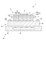
- FIG. 1 shows a power module substrate 10, a power module substrate 40 with a heat sink, and a power module 1 according to the first embodiment of the present invention.
- the power module 1 includes a power module substrate 40 with a heat sink, and a semiconductor element (electronic component) bonded to one surface (upper side in FIG. 1) of the power module substrate 40 with a heat sink via a solder layer 2. 3 is provided.
- the solder layer 2 is made of, for example, a Sn—Ag, Sn—In, or Sn—Ag—Cu solder material.
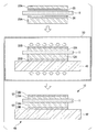
- the power module substrate 40 with a heat sink includes a power module substrate 10 and a heat sink 41 that cools the power module substrate 10.
- the heat sink 41 in the present embodiment includes a top plate portion 42 joined to the power module substrate 10, and a cooling member 43 stacked on the top plate portion 42.
- a flow path 44 through which a cooling medium flows is formed inside the cooling member 43.
- the top plate portion 42 and the cooling member 43 are connected by a fixing screw 45.
- the top plate portion 42 of the heat sink 41 is made of a metal material having a proof stress of 100 N / mm 2 or more, and the thickness thereof is 2 mm or more.
- the top plate portion 42 is made of an A6063 alloy (aluminum alloy).
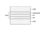
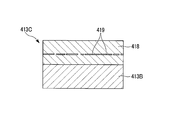
- the power module substrate 10 includes an insulating substrate 11, a circuit layer 12 disposed on one surface of the insulating substrate 11 (upper surface in FIG. 1), and the other surface (lower surface in FIG. 1) of the insulating substrate 11. And a disposed metal layer 13.
- the insulating substrate 11 prevents electrical connection between the circuit layer 12 and the metal layer 13, and is, for example, AlN (aluminum nitride), Si 3 N 4 (silicon nitride), Al 2 O 3 (alumina). In this embodiment, it is made of AlN (aluminum nitride).
- the thickness of the insulating substrate 11 is set within a range of 0.2 mm to 1.5 mm, for example, and is set to 0.635 mm in the present embodiment.
- the circuit layer 12 is bonded to the first aluminum layer 12A disposed on one surface (the upper surface in FIG. 1) of the insulating substrate 11 and one side of the first aluminum layer 12A. And a first copper layer 12B.
- the first aluminum layer 12A is formed by joining a rolled plate of aluminum (so-called 4N aluminum) having a purity of 99.99 mass% or more to one surface of the insulating substrate 11.
- the first copper layer 12B is formed by solid-phase diffusion bonding a rolled plate of oxygen-free copper to the first aluminum layer 12A.
- the metal layer 13 includes a second aluminum layer 13A disposed on the other surface (lower surface in FIG. 1) of the insulating substrate 11, and the other side of the second aluminum layer 13A (in FIG. 1). And a second copper layer 13B bonded to the lower side.
- the second aluminum layer 13A is formed by joining an aluminum (so-called 4N aluminum) rolled plate having a purity of 99.99 mass% or more to the other surface of the insulating substrate 11.
- the second copper layer 13B is formed by solid-phase diffusion bonding a rolled plate of oxygen-free copper to the second aluminum layer 13A.
- the circuit layer 12 and the metal layer 13 are respectively an aluminum layer (first aluminum layer 12A and second aluminum layer 13A) and a copper layer (first copper layer 12B and second copper layer). 13B) and a joined body obtained by solid phase diffusion bonding.
- first aluminum layer 12A and the first copper layer 12B and the bonding interface between the second aluminum layer 13A and the second copper layer 13B that are solid phase diffusion bonded are shown in FIGS.
- the intermetallic compound layers (the first intermetallic compound layer 12C and the second intermetallic compound layer 13C) are formed.
- the intermetallic compound layer (the first intermetallic compound layer 12C, the second intermetallic compound layer 13C) includes the aluminum atoms of the aluminum layer (the first aluminum layer 12A and the second aluminum layer 13A) and the copper layer (the first copper layer). 12B and the second copper layer 13B) are formed by interdiffusion with each other, and from the aluminum layer (first aluminum layer 12A, second aluminum layer 13A) to the copper layer (first copper layer 12B, second As it goes to the copper layer 13B), the concentration of aluminum atoms gradually decreases, and the concentration of copper atoms increases.
- the thickness t C of the intermetallic compound layers is in the range of 1 ⁇ m to 80 ⁇ m, preferably in the range of 5 ⁇ m to 80 ⁇ m. Is set.
- the intermetallic compound layers are composed of an intermetallic compound composed of Cu and Al.
- a plurality of intermetallic compounds are bonded at the interface. It is set as the structure laminated
- a structure in which three kinds of intermetallic compounds are stacked is used, and a copper layer is formed from the aluminum layer (first aluminum layer 12A, second aluminum layer 13A) side.
- a ⁇ phase 16 In order toward the (first copper layer 12B, second copper layer 13B) side, there are a ⁇ phase 16, a ⁇ 2 phase 17, and a ⁇ 2 phase 18 (see FIG. 13).
- the bonding interface between the intermetallic compound layer (the first intermetallic compound layer 12C and the second intermetallic compound layer 13C) and the copper layer (the first copper layer 12B and the second copper layer 13B) is along the bonding interface.
- the oxide 19 is dispersed in layers.
- the oxide 19 is an aluminum oxide such as alumina (Al 2 O 3 ).
- the oxide 19 was divided at the interface between the intermetallic compound layer (the first intermetallic compound layer 12C and the second intermetallic compound layer 13C) and the copper layer (the first copper layer 12B and the second copper layer 13B). There is also a region where the first intermetallic compound layer 12C and the first copper layer 12B are in direct contact with each other.
- the average crystal grain size of the copper layers (first copper layer 12B, second copper layer 13B) is in the range of 50 ⁇ m to 200 ⁇ m, and the aluminum layer (first aluminum layer 12A, second aluminum layer).
- the average crystal grain size of the layer 13A) is 500 ⁇ m or more.
- the thickness t 1 of the circuit layer 12 is set in a range of 0.10 mm ⁇ t 1 ⁇ 3.6 mm
- the thickness t 2 of the second aluminum layer 13A of the metal layer 13 is 0.15 mm
- ⁇ t 2 is set in the range of ⁇ 5.4 mm
- the thickness t 1 of the circuit layer 12 is t 2 / t 1 ⁇ 1.5.
- the first aluminum is formed on one surface (upper surface in FIG. 5) and the other surface (lower surface in FIG. 5) of the insulating substrate 11 via Al—Si based brazing materials 25 and 26.
- a plate 22A and a second aluminum plate 23A are stacked.
- the insulating substrate 11 is bonded to the first aluminum plate 22A and the second aluminum plate 23A by cooling after pressing and heating, and the first aluminum layer 12A and the second aluminum layer 13A are bonded to the insulating substrate 11.
- the brazing temperature is set to 640 ° C. to 650 ° C., for example.
- the first copper plate 22B is disposed on one side (the upper side in FIG. 5) of the first aluminum layer 12A. Further, the top plate portion 42 of the heat sink 41 is laminated on the other side (lower side in FIG. 5) of the second aluminum layer 13A via the second copper plate 23B. Then, it was placed in a vacuum heating furnace 50, and the pressure in the stacking direction (e.g. 3 kgf / cm 2 or more 35 kgf / cm 2 or less in pressure in a pressurized), heat treatment is performed in a vacuum atmosphere.
- the heating temperature is set to, for example, 400 ° C. or more and less than 548 ° C.
- the holding time is set to, for example, 5 minutes or more and 240 minutes or less.
- the heating temperature is preferably in the range of eutectic temperature of Al and Cu of ⁇ 5 ° C. or higher and lower than the eutectic temperature.
- the joint surface to be solid phase diffusion-bonded is smoothed by removing scratches on the surface in advance.
- a first copper layer 12B solid-phase diffusion bonded to the first aluminum layer 12A and a second copper layer 13B solid-phase diffusion bonded to the second aluminum layer 13A are formed (copper layer forming step S02).
- the second copper layer 13B and the top plate portion 42 are bonded by solid phase diffusion bonding (heat sink bonding step S03).
- the cooling member 43 is stacked on the other side of the top plate portion 42 with grease, and the top plate portion 42 and the cooling member 43 are connected by the fixing screws 45 (cooler connection step S04). Then, the semiconductor element 3 is bonded to one surface of the circuit layer 12 by solder (semiconductor element bonding step S05). In this way, the power module substrate 10, the power module substrate with heat sink 40, and the power module 1 according to the present embodiment are manufactured.
- the circuit layer 12 since the circuit layer 12 includes the first aluminum layer 12A on the insulating substrate 11 side, the difference in thermal expansion coefficient between the insulating substrate 11 and the circuit layer 12 when a heat cycle is applied. By absorbing the thermal stress generated due to the deformation of the first aluminum layer 12A, the insulating substrate 11 can be prevented from cracking.
- the first aluminum layer 12A is constituted by joining 4N aluminum rolled plates having a purity of 99.99 mass% or more, so that the deformation resistance is small and the thermal stress is absorbed, thereby the insulating substrate. 11 can be reliably suppressed.
- the circuit layer 12 includes the first copper layer 12B
- the heat from the semiconductor element 3 can be spread in the surface direction by the first copper layer 12B, and heat can be efficiently radiated. Further, the semiconductor element 3 can be satisfactorily soldered on the circuit layer 12 (first copper layer 12B).
- the first copper layer 12B has a relatively large deformation resistance, the surface of the circuit layer 12 can be prevented from being deformed when a power cycle is applied, and a crack or the like is generated in the solder layer 2. Can be suppressed.
- the 1st copper layer 12B is comprised by joining the rolled board of an oxygen free copper, it is excellent in thermal conductivity, and can improve a thermal radiation characteristic reliably. Since the first aluminum layer 12A and the first copper layer 12B are bonded by solid phase diffusion bonding, the first aluminum layer 12A and the first copper layer 12B are securely bonded, and the circuit layer 12 The thermal conductivity and electrical conductivity of can be maintained.
- the metal layer 13 has the second aluminum layer 13A bonded to the insulating substrate 11 and the second copper layer 13B bonded to the second aluminum layer 13A by solid phase diffusion bonding, the power module The thermal stress applied to the working substrate 10 is alleviated by the deformation of the second aluminum layer 13A, so that the insulating substrate 11 can be prevented from cracking. Furthermore, since heat is spread in the surface direction by the second copper layer 13B, the heat dissipation characteristics can be improved. Further, since the second aluminum layer 13A and the second copper layer 13B are bonded by solid phase diffusion bonding, the second aluminum layer 13A and the second copper layer 13B are securely bonded, and the metal layer 13 The thermal conductivity of can be maintained.
- an intermetallic compound layer (first aluminum layer 12A, second aluminum layer 13A) and a copper layer (first copper layer 12B, second copper layer 13B) are provided between the aluminum layer (first aluminum layer 12A, second aluminum layer 13A).
- a first intermetallic compound layer 12C and a second intermetallic compound layer 13C) are formed. Therefore, Al in the aluminum layer (first aluminum layer 12A, second aluminum layer 13A) is directed to the copper layer (first copper layer 12B, second copper layer 13B) side, and the copper layer (first copper layer 12B, second aluminum layer).
- Cu in the copper layer 13B) is sufficiently interdiffused to the aluminum layer (first aluminum layer 12A, second aluminum layer 13A) side, and the aluminum layer (first aluminum layer 12A, second aluminum layer 13A). And the copper layer (the first copper layer 12B and the second copper layer 13B) are securely bonded, and the bonding reliability is excellent.
- the bonding interface between the copper layer (first copper layer 12B and second copper layer 13B) and the intermetallic compound layer (first intermetallic compound layer 12C and second intermetallic compound layer 13C) The oxides 19 are dispersed in layers along these bonding interfaces. Therefore, the oxide film formed on the surface of the aluminum layer (the first aluminum layer 12A and the second aluminum layer 13A) is surely destroyed, and the mutual diffusion of Cu and Al is sufficiently advanced.
- the (first aluminum layer 12A, second aluminum layer 13A) and the copper layer (first copper layer 12B, second copper layer 13B) are securely bonded, and peeling may occur in the circuit layer 12 and the metal layer 13 There is no.
- the intermetallic compound layers (the first intermetallic compound layer 12C and the second intermetallic compound layer 13C) have a structure in which a plurality of intermetallic compounds are stacked along the bonding interface. It can suppress that a brittle intermetallic compound grows large.
- the ⁇ phase 16 and the ⁇ 2 phase are sequentially arranged from the aluminum layer (first aluminum layer 12A, second aluminum layer 13A) to the copper layer (first copper layer 12B, second copper layer 13B) side. 17 and ⁇ 2 phase 18 intermetallic compounds are laminated, so that the volume fluctuation inside the intermetallic compound layers (the first intermetallic compound layer 12C and the second intermetallic compound layer 13C) is reduced, and the internal strain is suppressed. Will be.
- Cu in the copper layer (first copper layer 12B, second copper layer 13B) and Al in the aluminum layer (first aluminum layer 12A, second aluminum layer 13A) mutually diffuse, From the copper layer (first copper layer 12B, second copper layer 13B) side to the aluminum layer (first aluminum layer 12A, second aluminum layer 13A) side, intermetallic compounds suitable for each composition are layered. Since it is formed, the characteristics of the bonding interface can be stabilized.
- the average crystal grain size of the aluminum layers is 500 ⁇ m or more, and the copper layers (the first copper layer 12B and the second copper layer 13B)
- the average crystal grain size is in the range of 50 ⁇ m to 200 ⁇ m. Therefore, excessive strain or the like is not accumulated in the aluminum layers (the first aluminum layer 12A and the second aluminum layer 13A), and the fatigue characteristics are improved. Therefore, the reliability with respect to the thermal stress which generate
- the thickness t C of the intermetallic compound layers is in the range of 1 ⁇ m to 80 ⁇ m, preferably 5 ⁇ m to 80 ⁇ m.
- the mutual diffusion of Cu and Al is sufficiently advanced, and the copper layer (first copper layer 12B, second copper layer 13B) and the aluminum layer (first aluminum layer 12A, second aluminum layer 13A) are firmly formed.
- the brittle intermetallic compound is prevented from growing more than necessary, and the characteristics of the joint interface are stabilized.
- the metal layer 13 having the second aluminum layer 13A is interposed between the top plate portion 42 of the heat sink 41 and the insulating substrate 11, and this
- the thickness t 2 of the second aluminum layer 13A is set to t 1 ⁇ t 2 with respect to the thickness t 1 of the circuit layer 12. Therefore, the thermal strain caused by the difference in thermal expansion coefficient between the insulating substrate 11 and the heat sink 41 can be alleviated by the deformation of the second aluminum layer 13A of the metal layer 13, and the cracking of the insulating substrate 11 can be suppressed. it can.
- the metal layer 13 has the second copper layer 13B, and the second copper layer 13B and the top plate portion 42 of the heat sink 41 are joined by solid phase diffusion bonding.
- the heat on the substrate 10 side can be efficiently transferred to the heat sink 41 side, and the heat dissipation characteristics can be greatly improved.
- heat from the semiconductor element 3 mounted on the circuit layer 12 can be efficiently dissipated, and the power density (heat generation amount) of the semiconductor element 3 is improved. Even in such a case, it is possible to respond sufficiently. Further, durability during power cycle loading can be improved.
- a power module 101 shown in FIG. 6 includes a power module substrate 140 with a heat sink and a semiconductor bonded to one surface (the upper side in FIG. 6) of the power module substrate 140 with a heat sink via a first solder layer 102. And an element (electronic component) 3.
- the first solder layer 102 is made of, for example, a Sn—Ag, Sn—In, Sn—Sb, or Sn—Ag—Cu solder material.
- the power module substrate 140 with heat sink includes a power module substrate 110 and a heat sink 141 that cools the power module substrate 110.
- the power module substrate 110 has an insulating substrate 111, a circuit layer 112 disposed on one surface (upper surface in FIG. 6) of the insulating substrate 111, and the other surface (lower surface in FIG. 6) of the insulating substrate 111. And a disposed metal layer 113.
- the insulating substrate 111 is made of AlN (aluminum nitride).
- the thickness of the insulating substrate 111 is set within a range of, for example, 0.2 mm or more and 1.5 mm or less, and is set to 0.635 mm in the present embodiment.
- the circuit layer 112 is bonded to a first aluminum layer 112A disposed on one surface (the upper surface in FIG. 6) of the insulating substrate 111 and one side of the first aluminum layer 112A.
- a first copper layer 112B disposed on one surface (the upper surface in FIG. 6) of the insulating substrate 111 and one side of the first aluminum layer 112A.
- the first copper layer 112B is formed by joining a rolled plate of aluminum (so-called 4N aluminum) having a purity of 99.99 mass% or more to one surface of the insulating substrate 111.
- the first copper layer 112B is formed by solid-phase diffusion bonding a rolled plate of oxygen-free copper to the first aluminum layer 112A.
- the metal layer 113 includes a second aluminum layer 113A disposed on the other surface (the lower surface in FIG. 6) of the insulating substrate 111 and the other side of the second aluminum layer 113A (in FIG. 6). 2nd copper layer 113B joined to (lower side).
- the second aluminum layer 113A is formed by joining a rolled plate of aluminum (so-called 4N aluminum) having a purity of 99.99 mass% or more to the other surface of the insulating substrate 111.
- the second copper layer 113B is formed by solid-phase diffusion bonding a rolled plate of oxygen-free copper to the second aluminum layer 113A.
- the circuit layer 112 and the metal layer 113 are respectively formed of an aluminum layer (first aluminum layer 112A and second aluminum layer 113A) and a copper layer (first copper layer).
- the layer 112B and the second copper layer 113B) are composed of a joined body obtained by diffusion bonding.
- the power module substrate 110 is a present embodiment, the thickness t 1 of the circuit layer 112, the relationship between the thickness t 2 of the second aluminum layer 113A of metal layer 113, and t 1 ⁇ t 2 Has been.
- the thickness t 1 of the circuit layer 112 is set within a range of 0.1 mm ⁇ t 1 ⁇ 3.6 mm, and the thickness t 2 of the second aluminum layer 113A of the metal layer 113 is 0.15 mm.
- ⁇ t 2 is set in the range of ⁇ 5.4 mm
- the thickness t 1 of the circuit layer 112 the relationship between the thickness t 2 of the second aluminum layer 113A of metal layer 113 is t 2 / t 1 ⁇ 1.5.
- the heat sink 141 in the present embodiment is a heat radiating plate made of copper or a copper alloy.
- the heat sink 141 is bonded to the metal layer 113 of the power module substrate 110 via the second solder layer 108.
- the second solder layer 108 is made of various solder materials such as Sn—Ag, Sn—In, Sn—Sb, or Sn—Ag—Cu, like the first solder layer 102 described above. be able to.
- the cracking of the insulating substrate 111 and the warpage of the power module substrate 110 are suppressed as in the first embodiment. Can do. Furthermore, in the present embodiment, since the metal layer 113 has the second copper layer 113B, the heat sink 141 made of copper or a copper alloy can be joined via the solder layer 108.
- the circuit layer 112 has the first copper layer 112B and the metal layer 113 has the second copper layer 113B, the rigidity of the entire power module substrate 110 is ensured, and the thermal cycle load Sometimes, the power module substrate 110 is hardly deformed, and the occurrence of cracks in the second solder layer 108 can be suppressed.
- a power module 201 shown in FIG. 7 includes a power module substrate 240 with a heat sink and a semiconductor element (bonded to the surface on one side (the upper side in FIG. 7) of the power module substrate 240 with a heat sink via a solder layer 202 ( Electronic component) 3.
- the solder layer 202 is made of, for example, a Sn—Ag, Sn—In, or Sn—Ag—Cu solder material.
- the power module substrate 240 with a heat sink includes a power module substrate 210 and a heat sink 241 for cooling the power module substrate 210.
- the power module substrate 210 has an insulating substrate 211, a circuit layer 212 disposed on one surface (the upper surface in FIG. 7) of the insulating substrate 211, and the other surface (lower surface in FIG. 7) of the insulating substrate 211. And a disposed metal layer 213.
- the insulating substrate 211 is made of AlN (aluminum nitride).
- the thickness of the insulating substrate 211 is set, for example, within a range of 0.2 mm or more and 1.5 mm or less, and is set to 0.635 mm in this embodiment.
- the circuit layer 212 is joined to the first aluminum layer 212A disposed on one surface (the upper surface in FIG. 7) of the insulating substrate 211 and to one side of the first aluminum layer 212A.
- a first copper layer 212B a first copper layer 212B.
- the first aluminum layer 212A is formed by joining a rolled plate of aluminum (so-called 4N aluminum) having a purity of 99.99 mass% or more to one surface of the insulating substrate 211.
- the first copper layer 212B is formed by solid-phase diffusion bonding a rolled plate of oxygen-free copper to the first aluminum layer 212A.
- the metal layer 213 includes a second aluminum layer 213 ⁇ / b> A disposed on the other surface (the lower surface in FIG. 7) of the insulating substrate 211.
- the metal layer 213 (second aluminum layer 213A) is formed by joining a rolled sheet of aluminum (so-called 4N aluminum) having a purity of 99.99 mass% or more to the other surface of the insulating substrate 211. Has been.
- the power module substrate 210 is a present embodiment, the thickness t 1 of the circuit layer 212, the relationship between the thickness t 2 of the second aluminum layer 213A of metal layer 213, and t 1 ⁇ t 2 Has been.
- the thickness t 1 of the circuit layer 212 is set within a range of 0.1 mm ⁇ t 1 ⁇ 3.6 mm, and the thickness t 2 of the metal layer 213 (second aluminum layer 213A) is set to be 0.00.
- 15 mm ⁇ t 2 is set in the range of ⁇ 5.4 mm, the thickness t 1 of the circuit layer 212, the metal layer 213 relationship between the thickness t 2 (second aluminum layer 213A) is t 2 / t 1 ⁇ 1.5.
- the heat sink 241 in the present embodiment is a cooler made of aluminum or an aluminum alloy, and includes a top plate portion 242 joined to the metal layer 213 and a flow path 244 through which the coolant flows. Yes.
- the heat sink 241 is joined to the metal layer 213 (second aluminum layer 213A) of the power module substrate 210 by brazing.
- the metal layer 213 is composed of the second aluminum layer 213A, it can be satisfactorily bonded to the heat sink 241 made of aluminum or an aluminum alloy by brazing.
- the aluminum plate used as the aluminum layer has been described as a 4N aluminum rolled plate having a purity of 99.99 mass% or more, but is not limited thereto. It may be composed of other aluminum or aluminum alloy.
- a copper plate used as a copper layer (a 1st copper layer, a 2nd copper layer), although it demonstrated as what uses a rolled plate of an oxygen free copper, it is not limited to this, Other copper or copper alloys It may be configured by.
- a ceramic substrate made of AlN as an insulating substrate is not limited thereto, for example, Si 3 N 4 or Al may be used a ceramic substrate made 2 O 3 or the like.
- a transient liquid phase bonding method Transient Liquid Phase Bonding
- a metal paste method, a casting method, or the like may be applied.
- the structure of the heat sink is not limited to the present embodiment, and may be a heat sink, a cooler, or the like having another structure, for example.
- the circuit layer 12 includes the first aluminum layer 12A formed on one surface of the insulating substrate 11, and the first copper plate 22B on one side of the first aluminum layer 12A.
- the circuit layer 312 is bonded to the first aluminum layer 312A formed on one surface of the insulating substrate 11 and one side of the first aluminum layer 312A.
- the first copper layer 312B may be formed of a copper plate having a die pad 332 to which a semiconductor element or the like is bonded and a lead portion 333 used as an external terminal.
- the die pad 332 and the first aluminum layer 312A are solid-phase diffusion bonded.
- the thickness of the first aluminum layer 312A is preferably 0.1 mm or more and 1.0 mm or less.
- the thickness of the 1st copper layer 312B shall be 0.1 mm or more and 6.0 mm or less.
- a heat sink 341 made of aluminum or an aluminum alloy is joined to the metal layer 13 side of the power module substrate 310 by solid phase diffusion bonding.
- an intermetallic compound layer is in the joining interface of an aluminum layer (1st aluminum layer 12A, 2nd aluminum layer 13A) and a copper layer (1st copper layer 12B, 2nd copper layer 13B).
- First intermetallic compound layer 12C, second intermetallic compound layer 13C is formed, and from the aluminum layer side (first aluminum layer 12A, second aluminum layer 13A) to the copper layer side (first copper layer 12B, second
- the present invention is not limited to this.
- a plurality of intermetallic compounds composed of Cu and Al may be laminated so that the ratio of aluminum decreases.
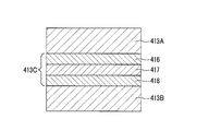
- aluminum is provided at the bonding interface between the aluminum layer (first aluminum layer 412A and second aluminum layer 413A) and the copper layer (first copper layer 412B and second copper layer 413B).
- the ⁇ phase 416 In order from the layer (first aluminum layer 412A, second aluminum layer 413A) side to the copper layer (first copper layer 412B, second copper layer 413B) side, along the aforementioned bonding interface, the ⁇ phase 416, ⁇ 2
- the intermetallic compound layer (the first intermetallic compound layer 412C and the second intermetallic compound) formed by laminating the phase 417 and further laminating at least one of the ⁇ 2 phase 418, the ⁇ phase 414, and the ⁇ 2 phase 415.
- a layer 413C may be provided (see FIG. 13).
- the oxide 19 is dispersed in layers along the bonding interface.
- the intermetallic compound layer first intermetallic compound layer 412C, second metal
- the oxide 419 is layered inside the ⁇ 2 phase 418, ⁇ phase 414, or ⁇ 2 phase 415 along the interface between the intermetallic compound layer 413C) and the copper layer (first copper layer 412B, second copper layer 413B).
- a distributed configuration may be adopted.
- the oxide 419 is an aluminum oxide such as alumina (Al 2 O 3 ).
- Example 1 A comparative experiment conducted to confirm the effectiveness of the present invention will be described. As shown in Table 1, an insulating substrate, an aluminum plate serving as a first aluminum layer of a circuit layer, a copper plate serving as a first copper layer, an aluminum plate serving as a second aluminum layer of a metal layer, and a copper plate serving as a second copper layer
- the power module substrate was manufactured by bonding.
- the size of the circuit layer was 37 mm ⁇ 37 mm
- the size of the insulating substrate was 40 mm ⁇ 40 mm
- the size of the metal layer was 37 mm ⁇ 37 mm.
- TLP TLP
- Cu is fixed to the surface of an insulating substrate so as to be 1.0 mg / cm 2, and is pressurized at 5 kgf / cm 2 in the stacking direction in a vacuum of 10 ⁇ 3 Pa. Then, the aluminum plate and the insulating substrate were joined by heating at 600 ° C. for 30 minutes.
- Table "Al-Si brazing” as shown in 2 using a brazing filler metal foil made of Al-7.5 wt% Si (thickness 100 [mu] m), in a state pressurized at 12 kgf / cm 2 in the stacking direction, 10 - The aluminum plate and the insulating substrate were joined by heating at 650 ° C. for 30 minutes in a 3 Pa vacuum.
- the “active metal brazing” shown in Table 2 uses an active brazing material composed of Ag-27.4 mass% Cu-2.0 mass% Ti in a vacuum of 10 ⁇ 3 Pa at 850 ° C. for 10 minutes.
- the copper plate and the insulating substrate were joined by heating.
- “DBC” shown in Table 2 joined the copper plate and the insulating substrate by heating at 1075 ° C. for 10 minutes in a nitrogen gas atmosphere.
- the solid phase diffusion bonding of the first copper layer and the first aluminum layer, and the second copper layer and the second aluminum layer was performed using a vacuum furnace using a furnace pressure of 3 ⁇ 10 ⁇ 3 Pa, a heating temperature of 535 ° C., and a holding time.
- the test was carried out under the conditions of 60 min and a pressure of 12 kgf / cm 2 (1.17 MPa).
- a heat sink was joined to the other surface side of the metal layer of the power module substrate described above.
- the heat sink was an A3003 alloy aluminum plate (60 mm ⁇ 70 mm ⁇ 5 mm).
- the substrate is heated at 610 ° C. in a vacuum using Al—Si brazing foil with a pressure of 3.0 kgf / cm 2. It was set as the joining by doing.
- the heat sink and the second copper layer were solid phase diffusion bonded at the time of the solid phase diffusion bonding described above.
- an IGBT element was soldered to one surface side of the circuit layer of these power module substrates.
- Sn—Ag—Cu solder was used for solder bonding, and bonding was performed at 300 ° C. in a hydrogen reducing atmosphere.
- a power cycle test was carried out using the power module thus obtained. The evaluation results are shown in Table 2. In addition, it evaluated by the raise rate of the thermal resistivity after loading a power cycle 100,000 times.
- the rate of increase in thermal resistance was measured as follows.
- the measurement conditions are shown below. Temperature difference: 80 ° C Temperature range: 55 ° C to 135 ° C (measured with a temperature sensing diode in the IGBT element) Energizing time: 6 seconds Cooling time: 4 seconds
- Comparative Example 1 in which the thickness t 1 of the circuit layer was formed thicker than the thickness t 2 of the second aluminum layer of the metal layer, cracks were observed in the insulating substrate in 3000 cycles or less in the thermal cycle test. Furthermore, an increase in thermal resistance was observed in the power cycle test.
- Comparative Example 2 in which the thickness t 1 of the circuit layer was the same as the thickness t 2 of the second aluminum layer of the metal layer, cracks were observed in the insulating substrate in 2000 cycles or less in the thermal cycle test. Furthermore, an increase in thermal resistance was observed in the power cycle test.
- Comparative Examples 3 and 4 in which the circuit layer was composed only of the first aluminum layer it was confirmed that the thermal resistance greatly increased in the power cycle test, although the results of the thermal cycle test were good.
- Comparative Examples 5 and 6 in which the circuit layer was composed only of the first copper layer cracks were observed in the insulating substrate in 1000 cycles or less in the thermal cycle test.
- heat dissipation from a heating element such as an electronic component mounted on a circuit layer can be promoted, and it has excellent power cycle characteristics and insulation at the time of a cold cycle load. It was confirmed that it is possible to provide a highly reliable power module substrate, a power module substrate with a heat sink, and a power module that can suppress the occurrence of cracks in the substrate.
- Example 2 Next, as shown in the second embodiment described above and FIG. 6, the metal layer and the heat sink of the power module substrate are joined via the second solder layer, and the joining rate in the second solder layer was evaluated. .
- Table 3 an insulating substrate, an aluminum plate serving as a first aluminum layer of a circuit layer, a copper plate serving as a first copper layer, an aluminum plate serving as a second aluminum layer of a metal layer, and a copper plate serving as a second copper layer
- the power module substrate was manufactured by bonding.
- the size of the circuit layer was 37 mm ⁇ 37 mm
- the size of the insulating substrate was 40 mm ⁇ 40 mm
- the size of the metal layer was 37 mm ⁇ 37 mm.
- “TLP” and “Al—Si solder” shown in Table 4 were used in the same joining method as in Example 1 and Table 2 described above.
- the heat sink was joined to the other surface side of the metal layer of the above-mentioned board for power modules via a solder material.
- an A3003 alloy aluminum plate 60 mm ⁇ 70 mm ⁇ 5 mm
- soldering was performed after forming a Ni plating film on the joint surface of the heat sink.
- Comparative Example 11 after the Ni plating film was formed also on the joint surface of the metal layer, soldering was performed.
- a heat cycle test was carried out using the power module substrate with a heat sink thus obtained.
- the cooling / heating cycle conditions were the same as in Example 1, and 3000 cooling / heating cycles were loaded.
- the joining rate in a 2nd solder layer was measured after joining initial stage and 3000 times of thermal cycle loading. The evaluation results are shown in Table 4.
- the present invention it is possible to promote the dissipation of heat from a heating element such as an electronic component mounted on a circuit layer, to have excellent power cycle characteristics, and to prevent generation of cracks in an insulating substrate during a cold cycle load. It can suppress and can improve reliability. Therefore, the present invention is industrially applicable.
Abstract
Description
本願は、2013年3月29日に日本に出願された特願2013-072677号、及び2013年10月17日に日本に出願された特願2013-216802号について優先権を主張し、その内容をここに援用する。 The present invention relates to a power module substrate, a power module substrate with a heat sink, and a power module used in a semiconductor device that controls a large current and a high voltage.
The present application claims priority on Japanese Patent Application No. 2013-072677 filed in Japan on March 29, 2013, and Japanese Patent Application No. 2013-216802 filed in Japan on October 17, 2013, and the contents thereof. Is hereby incorporated by reference.
このようなパワーモジュール基板では、回路層の上に、はんだ材を介してパワー半導体素子などの半導体素子が搭載される。
そして、金属層の他方の面側に、パワーモジュール用基板を冷却するためのヒートシンクが接合される。 Among semiconductor elements, a power semiconductor element for supplying electric power has a relatively high calorific value, and as a substrate on which it is mounted, for example, AlN (aluminum nitride), Al 2 O 3 (alumina), Si 3 N 4 A circuit layer in which a first metal plate is bonded to one surface side of an insulating substrate made of (silicon nitride), and a metal layer in which a second metal plate is bonded to the other surface side of the insulating substrate; , A power module substrate including the above is used.
In such a power module substrate, a semiconductor element such as a power semiconductor element is mounted on the circuit layer via a solder material.
And the heat sink for cooling the board | substrate for power modules is joined to the other surface side of a metal layer.
また、回路層及び金属層が比較的変形抵抗が高い銅板で構成されているので、冷熱サイクルが負荷された際に、絶縁基板と銅板との間に生じる熱応力によって絶縁基板に割れが発生するおそれがあった。 Incidentally, in the power module substrate and the power module substrate with a heat sink described in
In addition, since the circuit layer and the metal layer are made of a copper plate having a relatively high deformation resistance, the insulating substrate is cracked by the thermal stress generated between the insulating substrate and the copper plate when a thermal cycle is applied. There was a fear.
ここで、アルミニウムは、銅に比べて熱伝導率が低いため、回路層を構成する第一の金属板としてアルミニウム板を用いた場合には、回路層の上に搭載された電気部品等の発熱体からの熱を拡げて放散することが銅よりも劣ることになる。このため、電子部品の小型化や高出力化により、パワー密度が上昇した場合には、熱を十分に放散することができなくなるおそれがあった。よって、パワーサイクルを負荷した際の耐久性が低下するおそれがあった。また、アルミニウムは、表面に強固な酸化皮膜が形成されることから、アルミニウム板からなる回路層の上に半導体素子を直接はんだ接合することができず、Niめっき等を行う必要があった。 Moreover, in the power module substrate and the power module substrate with a heat sink described in
Here, since aluminum has a lower thermal conductivity than copper, when an aluminum plate is used as the first metal plate constituting the circuit layer, heat is generated from electrical components mounted on the circuit layer. It is inferior to copper to spread and dissipate heat from the body. For this reason, when the power density increases due to downsizing and high output of the electronic component, there is a possibility that heat cannot be sufficiently dissipated. Therefore, there is a possibility that durability when a power cycle is loaded may be reduced. In addition, since a strong oxide film is formed on the surface of aluminum, a semiconductor element cannot be directly solder-bonded on a circuit layer made of an aluminum plate, and Ni plating or the like has to be performed.
また、鋳造法によってヒートシンクを形成していることから、ヒートシンクの構造が比較的簡単になり、冷却能力の高いヒートシンクを形成することができず、熱の放散を促進することができないといった問題があった。 Furthermore, in the power module substrate with a heat sink described in
In addition, since the heat sink is formed by a casting method, the structure of the heat sink becomes relatively simple, a heat sink having a high cooling capacity cannot be formed, and heat dissipation cannot be promoted. It was.
また、例えば、このパワーモジュール用基板の金属層側にヒートシンクを接合した場合であっても、絶縁基板とヒートシンクとの熱膨張係数の差に起因する熱歪みを、十分に厚く形成された第2アルミニウム層が変形することによって緩和することができる。 In the power module substrate having this configuration, the thickness t 1 of the circuit layer having the first aluminum layer and the first copper layer disposed on one surface side of the insulating substrate and the other surface side of the insulating substrate is disposed. Since the relation between the thickness t 2 of the second aluminum layer of the formed metal layer is t 1 <t 2 , the metal layer is formed relatively thick when thermal stress is applied to the power module substrate. The second aluminum layer of the metal layer is deformed, and the occurrence of warpage in the power module substrate can be suppressed.
Further, for example, even when a heat sink is bonded to the metal layer side of the power module substrate, the thermal strain caused by the difference in thermal expansion coefficient between the insulating substrate and the heat sink is formed to be sufficiently thick. It can be mitigated by the deformation of the aluminum layer.
また、回路層が、銅又は銅合金からなる第1銅層を備えているので、第1銅層によって半導体素子等からの熱を面方向に拡げることができ、効率的に放熱することが可能となる。さらに、回路層の上に半導体素子等を良好にはんだ接合することができる。また、第1銅層は、比較的変形抵抗が大きいので、パワーサイクルが負荷された場合に、回路層の表面が変形することを抑制でき、はんだ層にクラック等が発生することを抑制できる。
そして、第1アルミニウム層と第1銅層とは、固相拡散接合によって接合されているので、第1アルミニウム層と第1銅層とが確実に接合されており、回路層の熱伝導性及び導電性を維持することができる。 Furthermore, in the power module substrate of the present invention, the circuit layer includes a first aluminum layer made of aluminum and an aluminum alloy on the insulating substrate side, so that when the heat cycle is applied, the insulating substrate and the circuit layer It is possible to absorb the thermal stress generated due to the difference in thermal expansion coefficient between the first aluminum layer and the crack of the insulating substrate.
In addition, since the circuit layer includes the first copper layer made of copper or copper alloy, the heat from the semiconductor element or the like can be spread in the surface direction by the first copper layer, and can be efficiently radiated. It becomes. Furthermore, a semiconductor element or the like can be satisfactorily soldered on the circuit layer. Further, since the first copper layer has a relatively large deformation resistance, it is possible to suppress the deformation of the surface of the circuit layer when a power cycle is applied, and to suppress the occurrence of cracks or the like in the solder layer.
And since the 1st aluminum layer and the 1st copper layer are joined by solid phase diffusion joining, the 1st aluminum layer and the 1st copper layer are joined firmly, and the thermal conductivity of circuit layers and Conductivity can be maintained.
この場合、絶縁基板の他方の面側に位置する金属層が、前記第2アルミニウム層と、この第2アルミニウム層に固相拡散接合された第2銅層と、を備えているので、このパワーモジュール用基板の金属層側にヒートシンクを接合する際には第2銅層とヒートシンクとが接合されることになる。
例えば、ヒートシンクの接合面がアルミニウム又はアルミニウム合金で構成されている場合には、この第2銅層とヒートシンクとを固相拡散接合法によって接合することが可能となる。また、例えば、ヒートシンクの接合面が銅又は銅合金で構成されている場合には、この第2銅層とヒートシンクとをはんだを用いて接合することが可能となる。 The metal layer may include the second aluminum layer bonded to the insulating substrate and a second copper layer made of copper or a copper alloy bonded to the second aluminum layer by solid phase diffusion bonding.
In this case, the metal layer located on the other surface side of the insulating substrate includes the second aluminum layer and a second copper layer bonded to the second aluminum layer by solid phase diffusion bonding. When the heat sink is bonded to the metal layer side of the module substrate, the second copper layer and the heat sink are bonded.
For example, when the bonding surface of the heat sink is made of aluminum or an aluminum alloy, the second copper layer and the heat sink can be bonded by a solid phase diffusion bonding method. For example, when the joining surface of the heat sink is made of copper or a copper alloy, the second copper layer and the heat sink can be joined using solder.
さらに、絶縁基板と第2銅層の間に比較的変形抵抗が小さい第2アルミニウム層が形成されているので、第2アルミニウム層が変形することによって熱応力が緩和されることになり、絶縁基板に割れが生じることを抑制できる。
そして、第2アルミニウム層と第2銅層とが、固相拡散接合によって接合されているので、第2アルミニウム層と第2銅層とが確実に接合されており、金属層の熱伝導性を維持することができる。 Moreover, since the metal layer is provided with the 2nd copper layer which consists of copper or a copper alloy, heat can be spread in a surface direction by a 2nd copper layer, and it becomes possible to thermally radiate efficiently.
Further, since the second aluminum layer having a relatively small deformation resistance is formed between the insulating substrate and the second copper layer, the second aluminum layer is deformed, so that the thermal stress is relieved, and the insulating substrate It can suppress that a crack arises.
And since the 2nd aluminum layer and the 2nd copper layer are joined by solid phase diffusion joining, the 2nd aluminum layer and the 2nd copper layer are joined firmly, and thermal conductivity of a metal layer is made. Can be maintained.
この場合、回路層の厚さt1と、金属層の第2アルミニウム層の厚さt2と、の関係が、t2/t1≧1.5とされているので、パワーモジュール用基板における反りの発生を確実に抑制することができる。 Relationship between the thickness t 2 of the second aluminum layer having a thickness of t 1 and the metal layer of the circuit layer, which is preferably a t 2 / t 1 ≧ 1.5.
In this case, the thickness t 1 of the circuit layer, the thickness t 2 of the second aluminum layer of the metal layer, the relationship, because there is a t 2 / t 1 ≧ 1.5, the power module substrate Warpage can be reliably suppressed.
この構成のヒートシンク付パワーモジュール用基板によれば、ヒートシンクと絶縁基板との間に、アルミニウム又はアルミニウム合金からなる第2アルミニウム層を有する金属層が介在しており、この第2アルミニウム層の厚さt2が、回路層の厚さt1に対して、t1<t2とされている。したがって、絶縁基板とヒートシンクとの熱膨張係数の差に起因する熱歪みを、金属層の第2アルミニウム層の変形によって緩和することができ、絶縁基板の割れを抑制することができる。 A power module substrate with a heat sink according to another aspect of the present invention includes the above-described power module substrate and a heat sink bonded to the metal layer side.
According to the power module substrate with a heat sink having this configuration, the metal layer having the second aluminum layer made of aluminum or aluminum alloy is interposed between the heat sink and the insulating substrate, and the thickness of the second aluminum layer is t 2 is t 1 <t 2 with respect to the thickness t 1 of the circuit layer. Therefore, thermal strain caused by the difference in thermal expansion coefficient between the insulating substrate and the heat sink can be alleviated by deformation of the second aluminum layer of the metal layer, and cracking of the insulating substrate can be suppressed.
この構成のパワーモジュールによれば、回路層上に搭載された電子部品からの熱を効率的に放散することができ、電子部品のパワー密度(発熱量)が向上した場合であっても、十分に対応することができる。また、パワーサイクル負荷時の耐久性を向上させることができる。 A power module according to another aspect of the present invention includes the above-described power module substrate and an electronic component mounted on the circuit layer.
According to the power module of this configuration, the heat from the electronic components mounted on the circuit layer can be efficiently dissipated, and even when the power density (heat generation amount) of the electronic components is improved, it is sufficient It can correspond to. Further, durability during power cycle loading can be improved.
図1は、本発明の第1の実施形態であるパワーモジュール用基板10、ヒートシンク付パワーモジュール用基板40及びパワーモジュール1を示す。
このパワーモジュール1は、ヒートシンク付パワーモジュール用基板40と、このヒートシンク付パワーモジュール用基板40の一方側(図1において上側)の面にはんだ層2を介して接合された半導体素子(電子部品)3と、を備えている。
ここで、はんだ層2は、例えばSn-Ag系、Sn-In系、若しくはSn-Ag-Cu系のはんだ材とされている。 Embodiments of the present invention will be described below with reference to the accompanying drawings.
FIG. 1 shows a
The
Here, the
本実施形態におけるヒートシンク41は、パワーモジュール用基板10と接合される天板部42と、この天板部42に積層配置される冷却部材43と、を備えている。冷却部材43の内部には、冷却媒体が流通する流路44が形成されている。 The
The
本実施形態では、第1アルミニウム層12Aは、絶縁基板11の一方の面に、純度が99.99mass%以上のアルミニウム(いわゆる4Nアルミニウム)の圧延板が接合されることで形成されている。
また、第1銅層12Bは、無酸素銅の圧延板が、第1アルミニウム層12Aに固相拡散接合されることによって形成されている。 As shown in FIG. 1, the
In the present embodiment, the
The
本実施形態では、第2アルミニウム層13Aは、絶縁基板11の他方の面に、純度が99.99mass%以上のアルミニウム(いわゆる4Nアルミニウム)の圧延板が接合されることで形成されている。
また、第2銅層13Bは、無酸素銅の圧延板が、第2アルミニウム層13Aに固相拡散接合されることによって形成されている。 As shown in FIG. 1, the
In the present embodiment, the
The
ここで、固相拡散接合された第1アルミニウム層12Aと第1銅層12Bの接合界面及び第2アルミニウム層13Aと第2銅層13Bの接合界面には、図2及び図3に示すように、それぞれ金属間化合物層(第1金属間化合物層12C、第2金属間化合物層13C)が形成されている。 Thus, in the present embodiment, the
Here, the bonding interface between the
本実施形態では、図2及び図3に示すように、3種の金属間化合物が積層された構造とされており、アルミニウム層(第1アルミニウム層12A、第2アルミニウム層13A)側から銅層(第1銅層12B、第2銅層13B)側に向けて順に、θ相16、η2相17、ζ2相18とされている(図13参照)。 The intermetallic compound layers (the first
In this embodiment, as shown in FIGS. 2 and 3, a structure in which three kinds of intermetallic compounds are stacked is used, and a copper layer is formed from the aluminum layer (
さらに、本実施形態では、銅層(第1銅層12B、第2銅層13B)の平均結晶粒径が50μm以上200μm以下の範囲内とされ、アルミニウム層(第1アルミニウム層12A、第2アルミニウム層13A)の平均結晶粒径が500μm以上とされている。 Further, the bonding interface between the intermetallic compound layer (the first
Furthermore, in this embodiment, the average crystal grain size of the copper layers (
本実施形態では、回路層12の厚さt1が0.10mm≦t1≦3.6mmの範囲内に設定され、金属層13の第2アルミニウム層13Aの厚さt2が、0.15mm≦t2≦5.4mmの範囲内に設定されており、回路層12の厚さt1と、金属層13の第2アルミニウム層13Aの厚さt2との関係がt2/t1≧1.5とされている。 Here, as shown in FIG. 1, the thickness t 1 of the
In the present embodiment, the thickness t 1 of the
これにより、第1アルミニウム層12Aに固相拡散接合された第1銅層12B及び第2アルミニウム層13Aに固相拡散接合された第2銅層13Bを形成する(銅層形成工程S02)。さらに、第2銅層13Bと天板部42とを固相拡散接合によって接合する(ヒートシンク接合工程S03)。 Next, the
Thus, a
そして、回路層12の一方の面に、はんだによって半導体素子3を接合する(半導体素子接合工程S05)。
このようにして、本実施形態であるパワーモジュール用基板10、ヒートシンク付パワーモジュール用基板40およびパワーモジュール1が製造される。 Next, the cooling
Then, the
In this way, the
特に、本実施形態では、回路層12の厚さt1と金属層13の第2アルミニウム層13Aの厚さt2との関係が、t2/t1≧1.5とされているので、パワーモジュール用基板10における反りの発生を確実に抑制することができる。 According to the
In particular, in this embodiment, the relationship between the thickness t 2 of the
また、回路層12(第1銅層12B)の上に半導体素子3を良好にはんだ接合することができる。さらに、第1銅層12Bは、比較的変形抵抗が大きいことから、パワーサイクルが負荷された場合に、回路層12の表面が変形することを抑制でき、はんだ層2にクラック等が発生することを抑制できる。特に、本実施形態では、第1銅層12Bが、無酸素銅の圧延板を接合することで構成されているので、熱伝導率に優れており、放熱特性を確実に向上させることができる。
そして、第1アルミニウム層12Aと第1銅層12Bとは、固相拡散接合によって接合されているので、第1アルミニウム層12Aと第1銅層12Bとが確実に接合されており、回路層12の熱伝導性及び導電性を維持することができる。 Furthermore, since the
Further, the
Since the
また、本実施形態では、アルミニウム層(第1アルミニウム層12A、第2アルミニウム層13A)から銅層(第1銅層12B、第2銅層13B)側に向けて順に、θ相16、η2相17、ζ2相18の金属間化合物がそれぞれ積層しているので、金属間化合物層(第1金属間化合物層12C、第2金属間化合物層13C)内部における体積変動が小さくなり、内部歪みが抑えられることになる。
すなわち、固相拡散しなかった場合、例えば、液相が形成された場合には、金属間化合物が必要以上に発生し、金属間化合物層はその体積の変動が大きくなり、金属間化合物層に内部歪みが生じる。しかし、固相拡散した場合には、脆い金属間化合物層が大きく成長せずに、金属間化合物が層状に形成されるため、その内部歪みが抑えられる。 In the present embodiment, the intermetallic compound layers (the first
In this embodiment, the
That is, when solid phase diffusion is not performed, for example, when a liquid phase is formed, an intermetallic compound is generated more than necessary, and the volume of the intermetallic compound layer increases, and the intermetallic compound layer Internal distortion occurs. However, in the case of solid phase diffusion, the brittle intermetallic compound layer does not grow greatly, and the intermetallic compound is formed in a layer form, so that the internal strain is suppressed.
さらに、本実施形態では、金属層13が第2銅層13Bを有しており、この第2銅層13Bとヒートシンク41の天板部42とが固相拡散接合されているので、パワーモジュール用基板10側の熱を効率的にヒートシンク41側へ伝達することができ、放熱特性を大幅に向上させることができる。 Further, in the power module substrate with
Further, in the present embodiment, the
図6に示すパワーモジュール101は、ヒートシンク付パワーモジュール用基板140と、このヒートシンク付パワーモジュール用基板140の一方側(図6において上側)の面に第1はんだ層102を介して接合された半導体素子(電子部品)3と、を備えている。ここで、第1はんだ層102は、例えばSn-Ag系、Sn-In系、Sn-Sb系、若しくはSn-Ag-Cu系のはんだ材とされている。 Next, a second embodiment of the present invention will be described with reference to FIG.
A
本実施形態では、絶縁基板111は、AlN(窒化アルミ)で構成されている。また、絶縁基板111の厚さは、例えば0.2mm以上1.5mm以下の範囲内に設定されており、本実施形態では0.635mmに設定されている。 The
In the present embodiment, the insulating
本実施形態では、第1アルミニウム層112Aは、絶縁基板111の一方の面に、純度が99.99mass%以上のアルミニウム(いわゆる4Nアルミニウム)の圧延板が接合されることで形成されている。
また、第1銅層112Bは、無酸素銅の圧延板が、第1アルミニウム層112Aに固相拡散接合されることによって形成されている。 As shown in FIG. 6, the
In the present embodiment, the
The
本実施形態では、第2アルミニウム層113Aは、絶縁基板111の他方の面に、純度が99.99mass%以上のアルミニウム(いわゆる4Nアルミニウム)の圧延板が接合されることで形成されている。
また、第2銅層113Bは、無酸素銅の圧延板が、第2アルミニウム層113Aに固相拡散接合されることによって形成されている。 As shown in FIG. 1, the
In the present embodiment, the
The
本実施形態では、回路層112の厚さt1が0.1mm≦t1≦3.6mmの範囲内に設定され、金属層113の第2アルミニウム層113Aの厚さt2が、0.15mm≦t2≦5.4mmの範囲内に設定されており、回路層112の厚さt1と、金属層113の第2アルミニウム層113Aの厚さt2との関係がt2/t1≧1.5とされている。 Then, the
In the present embodiment, the thickness t 1 of the
このヒートシンク141は、パワーモジュール用基板110の金属層113と、第2はんだ層108を介して接合されている。また、第2はんだ層108は、上述の第1はんだ層102と同様に、例えばSn-Ag系、Sn-In系、Sn-Sb系、若しくはSn-Ag-Cu系等の各種はんだ材を用いることができる。 Further, the
The
さらに、本実施形態においては、金属層113が第2銅層113Bを有しているので、銅又は銅合金からなるヒートシンク141をはんだ層108を介して接合することができる。 In the
Furthermore, in the present embodiment, since the
図7に示すパワーモジュール201は、ヒートシンク付パワーモジュール用基板240と、このヒートシンク付パワーモジュール用基板240の一方側(図7において上側)の面にはんだ層202を介して接合された半導体素子(電子部品)3と、を備えている。ここで、はんだ層202は、例えばSn-Ag系、Sn-In系、若しくはSn-Ag-Cu系のはんだ材とされている。 Next, a third embodiment of the present invention will be described with reference to FIG.
A
本実施形態では、絶縁基板211は、AlN(窒化アルミ)で構成されている。また、絶縁基板211の厚さは、例えば0.2mm以上1.5mm以下の範囲内に設定されており、本実施形態では0.635mmに設定されている。 The
In the present embodiment, the insulating
本実施形態では、第1アルミニウム層212Aは、絶縁基板211の一方の面に、純度が99.99mass%以上のアルミニウム(いわゆる4Nアルミニウム)の圧延板が接合されることで形成されている。また、第1銅層212Bは、無酸素銅の圧延板が、第1アルミニウム層212Aに固相拡散接合されることによって形成されている。 As shown in FIG. 7, the
In the present embodiment, the first aluminum layer 212A is formed by joining a rolled plate of aluminum (so-called 4N aluminum) having a purity of 99.99 mass% or more to one surface of the insulating
本実施形態では、金属層213(第2アルミニウム層213A)は、絶縁基板211の他方の面に、純度が99.99mass%以上のアルミニウム(いわゆる4Nアルミニウム)の圧延板が接合されることで形成されている。 As shown in FIG. 7, the
In the present embodiment, the metal layer 213 (
本実施形態では、回路層212の厚さt1が0.1mm≦t1≦3.6mmの範囲内に設定され、金属層213(第2アルミニウム層213A)の厚さt2が、0.15mm≦t2≦5.4mmの範囲内に設定されており、回路層212の厚さt1と、金属層213(第2アルミニウム層213A)の厚さt2との関係がt2/t1≧1.5とされている。 Then, the
In the present embodiment, the thickness t 1 of the
このヒートシンク241は、パワーモジュール用基板210の金属層213(第2アルミニウム層213A)に、ろう付けによって接合されている。 In addition, the
The
さらに、本実施形態においては、金属層213が第2アルミニウム層213Aで構成されているので、アルミニウム又はアルミニウム合金からなるヒートシンク241と、ろう付けによって良好に接合することができる。 In the power module substrate with
Furthermore, in this embodiment, since the
例えば、アルミニウム層(第1アルミニウム層、第2アルミニウム層)となるアルミニウム板として、純度99.99mass%以上の4Nアルミニウムの圧延板を用いるものとして説明したが、これに限定されることはなく、他のアルミニウム又はアルミニウム合金で構成されたものであってもよい。同様に、銅層(第1銅層、第2銅層)となる銅板として、無酸素銅の圧延板を用いるものとして説明したが、これに限定されることはなく、他の銅又は銅合金で構成されたものであってもよい。 As mentioned above, although embodiment of this invention was described, this invention is not limited to this, It can change suitably in the range which does not deviate from the technical idea of the invention.
For example, the aluminum plate used as the aluminum layer (the first aluminum layer and the second aluminum layer) has been described as a 4N aluminum rolled plate having a purity of 99.99 mass% or more, but is not limited thereto. It may be composed of other aluminum or aluminum alloy. Similarly, as a copper plate used as a copper layer (a 1st copper layer, a 2nd copper layer), although it demonstrated as what uses a rolled plate of an oxygen free copper, it is not limited to this, Other copper or copper alloys It may be configured by.
さらに、絶縁基板と第1アルミニウム層及び第2アルミニウム層とをろう付けにて接合するものとして説明したが、これに限定されることはなく、例えば過渡液相接合法(Transient Liquid Phase Bonding)、金属ペースト法、鋳造法等を適用してもよい。
また、ヒートシンクの構造等は、本実施形態に限定されることはなく、例えば他の構造の放熱板、冷却器等であってもよい。 Also, have been described as using a ceramic substrate made of AlN as an insulating substrate is not limited thereto, for example, Si 3 N 4 or Al may be used a ceramic substrate made 2 O 3 or the like.
Furthermore, although it demonstrated as what joins an insulating substrate, a 1st aluminum layer, and a 2nd aluminum layer by brazing, it is not limited to this, For example, a transient liquid phase bonding method (Transient Liquid Phase Bonding), A metal paste method, a casting method, or the like may be applied.
The structure of the heat sink is not limited to the present embodiment, and may be a heat sink, a cooler, or the like having another structure, for example.
例えば図8のパワーモジュール用基板310に示すように、回路層312が、絶縁基板11の一方の面に形成された第1アルミニウム層312Aと、この第1アルミニウム層312Aの一方側に接合された第1銅層312Bとを備え、この第1銅層312Bは、半導体素子などが接合されるダイパッド332と、外部端子として用いられるリード部333とを有する銅板からなる構成とされても良い。このパワーモジュール用基板310では、ダイパッド332と第1アルミニウム層312Aとが固相拡散接合されている。ここで、第1アルミニウム層312Aの厚さは、0.1mm以上1.0mm以下とされていることが好ましい。また、第1銅層312Bの厚さは、0.1mm以上6.0mm以下とされていることが好ましい。
また、図8に示すヒートシンク付パワーモジュール用基板340では、アルミニウム又はアルミニウム合金からなるヒートシンク341が、パワーモジュール用基板310の金属層13側に、固相拡散接合により接合されている。 In the power module substrate of the above embodiment, the
For example, as shown in the
In the
具体的には、アルミニウム層(第1アルミニウム層、第2アルミニウム層)と銅層(第1銅層、第2銅層)との接合界面において、アルミニウム層(第1アルミニウム層、第2アルミニウム層)側から銅層(第1銅層、第2銅層)側に向けて順に、アルミニウムの比率が低くなるように複数のCu及びAlからなる金属間化合物が積層されていても良い。 Moreover, in said embodiment, an intermetallic compound layer is in the joining interface of an aluminum layer (
Specifically, the aluminum layer (first aluminum layer, second aluminum layer) at the bonding interface between the aluminum layer (first aluminum layer, second aluminum layer) and the copper layer (first copper layer, second copper layer). ) Side to the copper layer (first copper layer, second copper layer) side, a plurality of intermetallic compounds composed of Cu and Al may be laminated so that the ratio of aluminum decreases.
本発明の有効性を確認するために行った比較実験について説明する。
表1に示すように、絶縁基板、回路層の第1アルミニウム層となるアルミニウム板及び第1銅層となる銅板、金属層の第2アルミニウム層となるアルミニウム板及び第2銅層となる銅板を接合してパワーモジュール用基板を作製した。
回路層のサイズは37mm×37mm、絶縁基板のサイズは40mm×40mm、金属層のサイズは37mm×37mmとした。 (Example 1)
A comparative experiment conducted to confirm the effectiveness of the present invention will be described.
As shown in Table 1, an insulating substrate, an aluminum plate serving as a first aluminum layer of a circuit layer, a copper plate serving as a first copper layer, an aluminum plate serving as a second aluminum layer of a metal layer, and a copper plate serving as a second copper layer The power module substrate was manufactured by bonding.
The size of the circuit layer was 37 mm × 37 mm, the size of the insulating substrate was 40 mm × 40 mm, and the size of the metal layer was 37 mm × 37 mm.
表2に示す「Al-Siロウ」は、Al―7.5質量%Siからなるろう材箔(厚さ100μm)を用いて、積層方向に12kgf/cm2で加圧した状態で、10-3Paの真空中にて、650℃で30分加熱することによって、アルミニウム板と絶縁基板とを接合した。
表2に示す「活性金属ロウ」は、Ag-27.4質量%Cu-2.0質量%Tiからなる活性ろう材を用いて、10-3Paの真空中にて、850℃で10分加熱することによって、銅板と絶縁基板とを接合した。
表2に示す「DBC」は、窒素ガス雰囲気中で1075℃で10分加熱することにより、銅板と絶縁基板とを接合した。 In “TLP” shown in Table 2, Cu is fixed to the surface of an insulating substrate so as to be 1.0 mg / cm 2, and is pressurized at 5 kgf / cm 2 in the stacking direction in a vacuum of 10 −3 Pa. Then, the aluminum plate and the insulating substrate were joined by heating at 600 ° C. for 30 minutes.
Table "Al-Si brazing" as shown in 2, using a brazing filler metal foil made of Al-7.5 wt% Si (thickness 100 [mu] m), in a state pressurized at 12 kgf / cm 2 in the stacking direction, 10 - The aluminum plate and the insulating substrate were joined by heating at 650 ° C. for 30 minutes in a 3 Pa vacuum.
The “active metal brazing” shown in Table 2 uses an active brazing material composed of Ag-27.4 mass% Cu-2.0 mass% Ti in a vacuum of 10 −3 Pa at 850 ° C. for 10 minutes. The copper plate and the insulating substrate were joined by heating.
“DBC” shown in Table 2 joined the copper plate and the insulating substrate by heating at 1075 ° C. for 10 minutes in a nitrogen gas atmosphere.
金属層が第2アルミニウム層のみで構成されたパワーモジュール用基板については、Al-Siろう箔を用いて、3.0kgf/cm2で加圧した状態で、真空中にて、610℃で加熱することによる接合とした。
金属層が第2アルミニウム層及び第2銅層で構成されたパワーモジュール用基板については、上述の固相拡散接合時に、ヒートシンクと第2銅層とを固相拡散接合した。 A heat sink was joined to the other surface side of the metal layer of the power module substrate described above. The heat sink was an A3003 alloy aluminum plate (60 mm × 70 mm × 5 mm).
For a power module substrate in which the metal layer is composed of only the second aluminum layer, the substrate is heated at 610 ° C. in a vacuum using Al—Si brazing foil with a pressure of 3.0 kgf / cm 2. It was set as the joining by doing.
For the power module substrate in which the metal layer is composed of the second aluminum layer and the second copper layer, the heat sink and the second copper layer were solid phase diffusion bonded at the time of the solid phase diffusion bonding described above.
評価装置:エスペック株式会社製TSB-51
液相:フロリナート
温度条件:-40℃×5分 ←→ 125℃×5分 A heat cycle test was carried out using the power module substrate with a heat sink thus obtained. The evaluation results are shown in Table 2. In addition, observation was implemented every 500 cycles and it evaluated by the cycle number when the crack of an insulated substrate was confirmed. The measurement conditions are shown below.
Evaluation device: TSB-51 manufactured by ESPEC Corporation
Liquid phase: Fluorinert Temperature conditions: -40 ° C x 5 minutes ← → 125 ° C x 5 minutes
このようにして得られたパワーモジュールを用いて、パワーサイクル試験を実施した。評価結果を表2に示す。なお、パワーサイクルを10万回負荷した後の熱抵抗率の上昇率で評価した。 Further, an IGBT element was soldered to one surface side of the circuit layer of these power module substrates. Note that Sn—Ag—Cu solder was used for solder bonding, and bonding was performed at 300 ° C. in a hydrogen reducing atmosphere.
A power cycle test was carried out using the power module thus obtained. The evaluation results are shown in Table 2. In addition, it evaluated by the raise rate of the thermal resistivity after loading a power cycle 100,000 times.
温度差:80℃
温度範囲:55℃~135℃(IGBT素子内の温度センスダイオードで測定)
通電時間:6秒
冷却時間:4秒 The rate of increase in thermal resistance was measured as follows. The IGBT was heated by energizing it, and the temperature of the IGBT element was measured using a temperature sensing diode in the IGBT element. Further, the temperature of the cooling medium (ethylene glycol: water = 9: 1) flowing through the heat sink was measured. The value normalized by the temperature difference between the IGBT temperature and the cooling medium was defined as the thermal resistance increase rate. The measurement conditions are shown below.
Temperature difference: 80 ° C
Temperature range: 55 ° C to 135 ° C (measured with a temperature sensing diode in the IGBT element)
Energizing time: 6 seconds Cooling time: 4 seconds


回路層の厚さt1が金属層の第2アルミニウム層の厚さt2と同一とされた比較例2においては、冷熱サイクル試験において2000サイクル以下で絶縁基板に割れが認められた。さらに、パワーサイクル試験でも熱抵抗の上昇が認められた。 In Comparative Example 1 in which the thickness t 1 of the circuit layer was formed thicker than the thickness t 2 of the second aluminum layer of the metal layer, cracks were observed in the insulating substrate in 3000 cycles or less in the thermal cycle test. Furthermore, an increase in thermal resistance was observed in the power cycle test.
In Comparative Example 2 in which the thickness t 1 of the circuit layer was the same as the thickness t 2 of the second aluminum layer of the metal layer, cracks were observed in the insulating substrate in 2000 cycles or less in the thermal cycle test. Furthermore, an increase in thermal resistance was observed in the power cycle test.
回路層を第1銅層のみで構成した比較例5,6においては、冷熱サイクル試験において1000サイクル以下で絶縁基板に割れが認められた。 In Comparative Examples 3 and 4 in which the circuit layer was composed only of the first aluminum layer, it was confirmed that the thermal resistance greatly increased in the power cycle test, although the results of the thermal cycle test were good.
In Comparative Examples 5 and 6 in which the circuit layer was composed only of the first copper layer, cracks were observed in the insulating substrate in 1000 cycles or less in the thermal cycle test.
次に、上述の第2の実施形態及び図6に示すように、パワーモジュール用基板の金属層とヒートシンクとを第2はんだ層を介して接合し、この第2はんだ層における接合率について評価した。
表3に示すように、絶縁基板、回路層の第1アルミニウム層となるアルミニウム板及び第1銅層となる銅板、金属層の第2アルミニウム層となるアルミニウム板及び第2銅層となる銅板を接合してパワーモジュール用基板を作製した。
回路層のサイズは37mm×37mm、絶縁基板のサイズは40mm×40mm、金属層のサイズは37mm×37mmとした。
なお、表4に示す「TLP」、「Al-Siロウ」は、上述の実施例1及び表2と同様の接合方法とした。 (Example 2)
Next, as shown in the second embodiment described above and FIG. 6, the metal layer and the heat sink of the power module substrate are joined via the second solder layer, and the joining rate in the second solder layer was evaluated. .
As shown in Table 3, an insulating substrate, an aluminum plate serving as a first aluminum layer of a circuit layer, a copper plate serving as a first copper layer, an aluminum plate serving as a second aluminum layer of a metal layer, and a copper plate serving as a second copper layer The power module substrate was manufactured by bonding.
The size of the circuit layer was 37 mm × 37 mm, the size of the insulating substrate was 40 mm × 40 mm, and the size of the metal layer was 37 mm × 37 mm.
Note that “TLP” and “Al—Si solder” shown in Table 4 were used in the same joining method as in Example 1 and Table 2 described above.
Sn-Sb系はんだを用い、H2雰囲気下で200℃で5分間保持した後、300℃で10分間保持することではんだ付けを行い、その後N2雰囲気に置換し、冷却することにより、ヒートシンクを接合した。なお、ヒートシンクの接合面には、Niめっき膜を形成した後、はんだ付けを実施した。さらに、比較例11においては、金属層の接合面にもNiめっき膜を形成した後、はんだ付けを実施した。 And the heat sink was joined to the other surface side of the metal layer of the above-mentioned board for power modules via a solder material. As the heat sink, an A3003 alloy aluminum plate (60 mm × 70 mm × 5 mm) was used as in Example 1 described above.
Using a Sn—Sb solder, hold at 200 ° C. for 5 minutes in an H 2 atmosphere, and then solder by holding at 300 ° C. for 10 minutes, then replace with N 2 atmosphere and cool to heat sink Were joined. In addition, after forming a Ni plating film on the joint surface of the heat sink, soldering was performed. Furthermore, in Comparative Example 11, after the Ni plating film was formed also on the joint surface of the metal layer, soldering was performed.
そして、接合初期及び3000回の冷熱サイクル負荷後において、第2はんだ層における接合率を測定した。評価結果を表4に示す。 A heat cycle test was carried out using the power module substrate with a heat sink thus obtained. The cooling / heating cycle conditions were the same as in Example 1, and 3000 cooling / heating cycles were loaded.
And the joining rate in a 2nd solder layer was measured after joining initial stage and 3000 times of thermal cycle loading. The evaluation results are shown in Table 4.
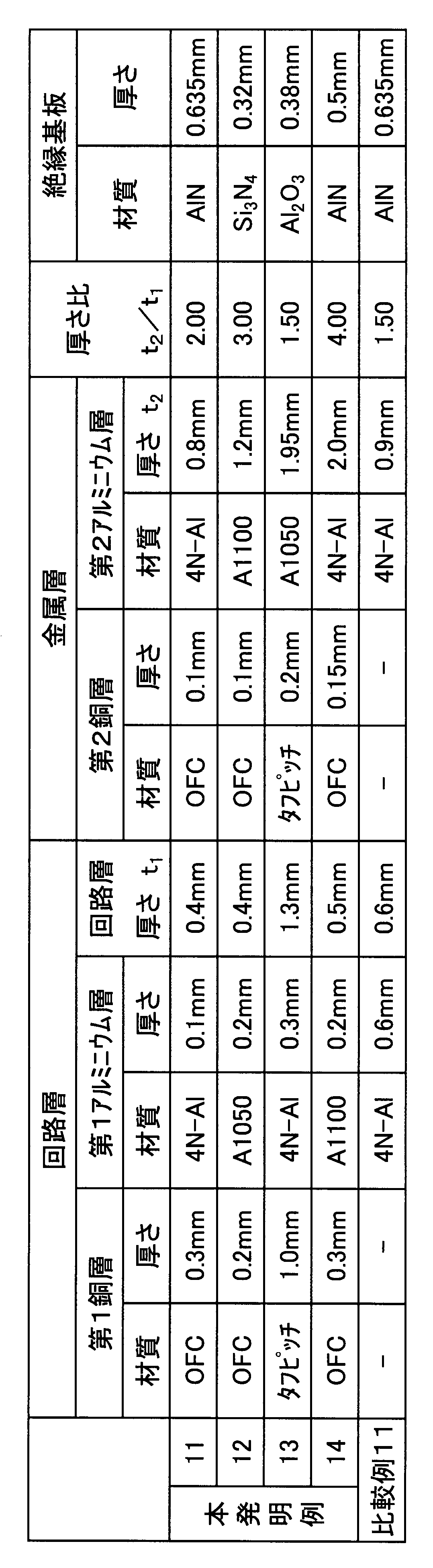
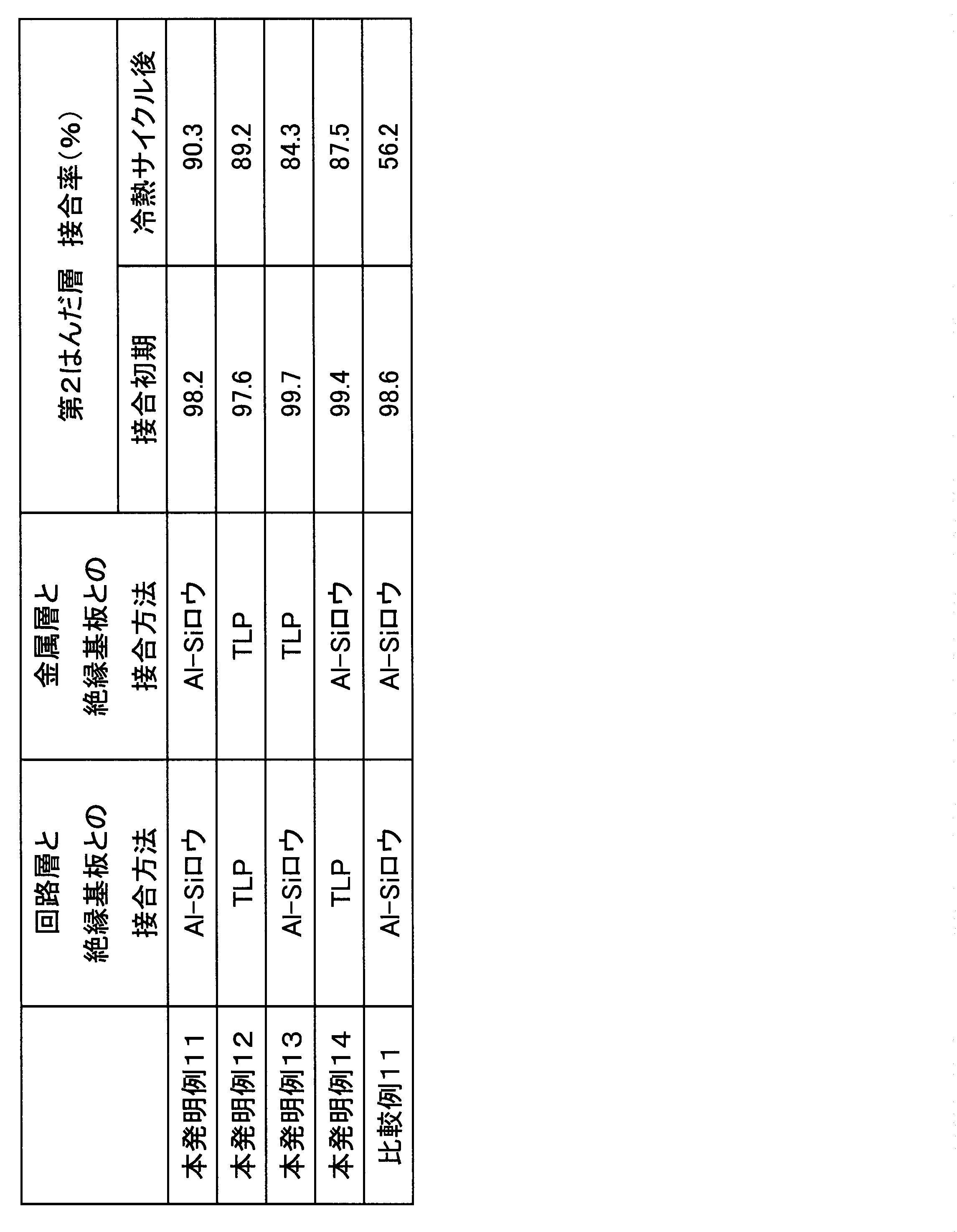
これに対して、本発明例11-14においては、冷熱サイクル後においても接合率が大きく低下しなかった。本発明例11-14によれば、第2はんだ層におけるクラックの発生を抑制できることが確認された。 In Comparative Example 11 in which the circuit layer and the metal layer were made of aluminum plates, the joining rate was greatly reduced after the cooling and heating cycle. It is presumed that cracks occurred in the second solder layer due to the cooling / heating cycle.
On the other hand, in Inventive Examples 11-14, the bonding rate did not significantly decrease even after the cooling / heating cycle. According to Invention Examples 11-14, it was confirmed that the occurrence of cracks in the second solder layer can be suppressed.
Claims (5)
- 絶縁基板と、該絶縁基板の一方の面に形成された回路層と、前記絶縁基板の他方の面に形成された金属層と、を備えたパワーモジュール用基板であって、
前記回路層は、前記絶縁基板に接合されたアルミニウム又はアルミニウム合金からなる第1アルミニウム層と、この第1アルミニウム層に固相拡散接合された銅又は銅合金からなる第1銅層と、を有し、
前記金属層は、アルミニウム又はアルミニウム合金からなる第2アルミニウム層を有しており、
前記回路層の厚さt1と前記金属層の第2アルミニウム層の厚さt2との関係が、t1<t2である、パワーモジュール用基板。 A power module substrate comprising: an insulating substrate; a circuit layer formed on one surface of the insulating substrate; and a metal layer formed on the other surface of the insulating substrate,
The circuit layer includes a first aluminum layer made of aluminum or an aluminum alloy bonded to the insulating substrate, and a first copper layer made of copper or a copper alloy bonded to the first aluminum layer by solid phase diffusion bonding. And
The metal layer has a second aluminum layer made of aluminum or an aluminum alloy,
Relationship between the thickness t 2 of the second aluminum layer having a thickness of t 1 and the metal layer of the circuit layer is t 1 <t 2, the power module substrate. - 前記金属層が、前記絶縁基板に接合された前記第2アルミニウム層と、この第2アルミニウム層に固相拡散接合された銅又は銅合金からなる第2銅層と、を有する、パワーモジュール用基板。 The power module substrate, wherein the metal layer includes the second aluminum layer bonded to the insulating substrate, and a second copper layer made of copper or a copper alloy bonded to the second aluminum layer by solid phase diffusion bonding. .
- 前記回路層の厚さt1と前記金属層の第2アルミニウム層の厚さt2との関係が、
t2/t1≧1.5である、請求項1又は請求項2に記載のパワーモジュール用基板。 Relationship between the thickness t 2 of the second aluminum layer having a thickness of t 1 and the metal layer of the circuit layer,
The power module substrate according to claim 1, wherein t 2 / t 1 ≧ 1.5. - 請求項1から請求項3のいずれか一項に記載のパワーモジュール用基板と、前記金属層側に接合されたヒートシンクと、を備える、ヒートシンク付パワーモジュール用基板。 A power module substrate with a heat sink, comprising: the power module substrate according to any one of claims 1 to 3; and a heat sink bonded to the metal layer side.
- 請求項1から請求項3のいずれか一項に記載のパワーモジュール用基板と、前記回路層上に搭載された電子部品と、を備える、パワーモジュール。 A power module comprising: the power module substrate according to any one of claims 1 to 3; and an electronic component mounted on the circuit layer.
Priority Applications (4)
| Application Number | Priority Date | Filing Date | Title |
|---|---|---|---|
| CN201480010107.2A CN105009278B (en) | 2013-03-29 | 2014-03-24 | Power module substrate, the power module substrate and power model for carrying radiator |
| KR1020157026040A KR102170623B1 (en) | 2013-03-29 | 2014-03-24 | Substrate for power modules, substrate with heat sink for power modules, and power module |
| EP14776236.3A EP2980844B1 (en) | 2013-03-29 | 2014-03-24 | Substrate for power modules, substrate with heat sink for power modules, and power module |
| US14/772,155 US9807865B2 (en) | 2013-03-29 | 2014-03-24 | Substrate for power modules, substrate with heat sink for power modules, and power module |
Applications Claiming Priority (4)
| Application Number | Priority Date | Filing Date | Title |
|---|---|---|---|
| JP2013072677 | 2013-03-29 | ||
| JP2013-072677 | 2013-03-29 | ||
| JP2013216802A JP6621076B2 (en) | 2013-03-29 | 2013-10-17 | Power module substrate, power module substrate with heat sink, and power module |
| JP2013-216802 | 2013-10-17 |
Publications (1)
| Publication Number | Publication Date |
|---|---|
| WO2014157112A1 true WO2014157112A1 (en) | 2014-10-02 |
Family
ID=51624085
Family Applications (1)
| Application Number | Title | Priority Date | Filing Date |
|---|---|---|---|
| PCT/JP2014/058132 WO2014157112A1 (en) | 2013-03-29 | 2014-03-24 | Substrate for power modules, substrate with heat sink for power modules, and power module |
Country Status (7)
| Country | Link |
|---|---|
| US (1) | US9807865B2 (en) |
| EP (1) | EP2980844B1 (en) |
| JP (1) | JP6621076B2 (en) |
| KR (1) | KR102170623B1 (en) |
| CN (1) | CN105009278B (en) |
| TW (1) | TWI621226B (en) |
| WO (1) | WO2014157112A1 (en) |
Cited By (2)
| Publication number | Priority date | Publication date | Assignee | Title |
|---|---|---|---|---|
| CN108140705A (en) * | 2015-09-25 | 2018-06-08 | 三菱综合材料株式会社 | Light emitting module substrate, light emitting module, the light emitting module substrate with refrigerator and light emitting module substrate manufacturing method |
| EP3375606A4 (en) * | 2015-11-11 | 2019-07-03 | NHK Spring Co., Ltd. | Laminate and laminate manufacturing method |
Families Citing this family (17)
| Publication number | Priority date | Publication date | Assignee | Title |
|---|---|---|---|---|
| WO2015147071A1 (en) * | 2014-03-25 | 2015-10-01 | 京セラ株式会社 | Passage member and semiconductor module |
| JP6384112B2 (en) * | 2014-04-25 | 2018-09-05 | 三菱マテリアル株式会社 | Power module substrate and power module substrate with heat sink |
| US9837363B2 (en) * | 2014-07-04 | 2017-12-05 | Mitsubishi Materials Corporation | Power-module substrate unit and power module |
| CN105742268B (en) * | 2014-12-26 | 2019-01-22 | 株式会社东芝 | Circuit board and semiconductor packages comprising circuit board |
| DE112015006049T5 (en) * | 2015-01-26 | 2017-10-12 | Mitsubishi Electric Corporation | SEMICONDUCTOR COMPONENT AND METHOD FOR PRODUCING A SEMICONDUCTOR COMPONENT |
| JP2016152383A (en) * | 2015-02-19 | 2016-08-22 | 三菱マテリアル株式会社 | Substrate for power module and power module |
| JP6702813B2 (en) * | 2016-06-27 | 2020-06-03 | 京セラ株式会社 | Composite substrate, electronic device and electronic module |
| EP3340293A1 (en) | 2016-12-20 | 2018-06-27 | Siemens Aktiengesellschaft | Semiconductor module with support structure on the bottom |
| CN110476244B (en) * | 2017-03-31 | 2023-11-03 | 罗姆股份有限公司 | Power module and method for manufacturing the same |
| US10886251B2 (en) * | 2017-04-21 | 2021-01-05 | Toyota Motor Engineering & Manufacturing North America, Inc. | Multi-layered composite bonding materials and power electronics assemblies incorporating the same |
| JP6601512B2 (en) | 2018-01-24 | 2019-11-06 | 三菱マテリアル株式会社 | Power module substrate with heat sink and power module |
| EP3770950A4 (en) * | 2018-03-23 | 2022-02-16 | Mitsubishi Materials Corporation | Method for manufacturing electronic-component-mounted module |
| JP6911805B2 (en) * | 2018-03-27 | 2021-07-28 | 三菱マテリアル株式会社 | Manufacturing method of insulated circuit board with heat sink |
| JP7147313B2 (en) * | 2018-07-18 | 2022-10-05 | 三菱マテリアル株式会社 | metal base substrate |
| JP7143659B2 (en) * | 2018-07-18 | 2022-09-29 | 三菱マテリアル株式会社 | metal base substrate |
| US10804236B2 (en) | 2018-10-25 | 2020-10-13 | Toyota Motor Engineering & Manufacturing North America, Inc. | Power electronic assemblies with high purity aluminum plated substrates |
| CN111755413A (en) * | 2020-07-07 | 2020-10-09 | 深圳基本半导体有限公司 | High-thermal-conductivity silicon carbide device packaging structure and method |
Citations (5)
| Publication number | Priority date | Publication date | Assignee | Title |
|---|---|---|---|---|
| JPS58181771A (en) * | 1982-04-16 | 1983-10-24 | 新明和工業株式会社 | Diffusion bonding method and composite body thereby |
| JPH04162756A (en) | 1990-10-26 | 1992-06-08 | Toshiba Corp | Semiconductor module |
| JP3171234B2 (en) | 1997-03-26 | 2001-05-28 | 三菱マテリアル株式会社 | Ceramic circuit board with heat sink |
| JP2002076551A (en) | 2000-09-04 | 2002-03-15 | Dowa Mining Co Ltd | Metal ceramic circuit board and its manufacturing method |
| JP2012064801A (en) * | 2010-09-16 | 2012-03-29 | Mitsubishi Materials Corp | Power module substrate with head sink, power module, and manufacturing method of power module substrate with head sink |
Family Cites Families (14)
| Publication number | Priority date | Publication date | Assignee | Title |
|---|---|---|---|---|
| JP3308883B2 (en) * | 1997-11-21 | 2002-07-29 | 電気化学工業株式会社 | Board |
| JP2003078086A (en) * | 2001-09-04 | 2003-03-14 | Kubota Corp | Lamination structure of semiconductor module substrate |
| JP3917503B2 (en) * | 2002-04-05 | 2007-05-23 | 住友精密工業株式会社 | Method of joining aluminum member and copper member and joining structure thereof |
| US8637777B2 (en) * | 2008-03-17 | 2014-01-28 | Mitsubishi Materials Corporation | Power module substrate having heatsink, method for manufacturing the same, power module having heatsink, and power module substrate |
| JP2010034238A (en) * | 2008-07-28 | 2010-02-12 | Shin Kobe Electric Mach Co Ltd | Wiring board |
| EP2477217B1 (en) * | 2009-09-09 | 2019-05-08 | Mitsubishi Materials Corporation | Method for producing substrate for power module with heat sink, substrate for power module with heat sink, and power module |
| CN102596488B (en) * | 2009-10-26 | 2013-09-18 | 株式会社新王材料 | Aluminum-bonding alloy, clad material having bonding alloy layer formed from the alloy, and composite material including bonded aluminum |
| WO2011155379A1 (en) * | 2010-06-08 | 2011-12-15 | 株式会社Neomaxマテリアル | Aluminum copper clad material |
| JP5463280B2 (en) * | 2010-12-28 | 2014-04-09 | 株式会社日立製作所 | Circuit board for semiconductor module |
| JP2012142320A (en) | 2010-12-28 | 2012-07-26 | Toyota Motor Corp | Semiconductor device manufacturing method |
| JP5548167B2 (en) * | 2011-07-11 | 2014-07-16 | 日本発條株式会社 | Laminate and method for producing laminate |
| JP3171234U (en) | 2011-08-09 | 2011-10-20 | 正宜 田辺 | Simple greenhouse |
| JP5786569B2 (en) | 2011-09-05 | 2015-09-30 | 三菱マテリアル株式会社 | Power module substrate manufacturing method |
| JP6307832B2 (en) * | 2013-01-22 | 2018-04-11 | 三菱マテリアル株式会社 | Power module board, power module board with heat sink, power module with heat sink |
-
2013
- 2013-10-17 JP JP2013216802A patent/JP6621076B2/en active Active
-
2014
- 2014-03-24 CN CN201480010107.2A patent/CN105009278B/en active Active
- 2014-03-24 WO PCT/JP2014/058132 patent/WO2014157112A1/en active Application Filing
- 2014-03-24 US US14/772,155 patent/US9807865B2/en active Active
- 2014-03-24 EP EP14776236.3A patent/EP2980844B1/en active Active
- 2014-03-24 KR KR1020157026040A patent/KR102170623B1/en active IP Right Grant
- 2014-03-27 TW TW103111491A patent/TWI621226B/en active
Patent Citations (5)
| Publication number | Priority date | Publication date | Assignee | Title |
|---|---|---|---|---|
| JPS58181771A (en) * | 1982-04-16 | 1983-10-24 | 新明和工業株式会社 | Diffusion bonding method and composite body thereby |
| JPH04162756A (en) | 1990-10-26 | 1992-06-08 | Toshiba Corp | Semiconductor module |
| JP3171234B2 (en) | 1997-03-26 | 2001-05-28 | 三菱マテリアル株式会社 | Ceramic circuit board with heat sink |
| JP2002076551A (en) | 2000-09-04 | 2002-03-15 | Dowa Mining Co Ltd | Metal ceramic circuit board and its manufacturing method |
| JP2012064801A (en) * | 2010-09-16 | 2012-03-29 | Mitsubishi Materials Corp | Power module substrate with head sink, power module, and manufacturing method of power module substrate with head sink |
Non-Patent Citations (1)
| Title |
|---|
| See also references of EP2980844A4 |
Cited By (4)
| Publication number | Priority date | Publication date | Assignee | Title |
|---|---|---|---|---|
| CN108140705A (en) * | 2015-09-25 | 2018-06-08 | 三菱综合材料株式会社 | Light emitting module substrate, light emitting module, the light emitting module substrate with refrigerator and light emitting module substrate manufacturing method |
| EP3355370A4 (en) * | 2015-09-25 | 2019-05-01 | Mitsubishi Materials Corporation | Light-emitting module substrate, light-emitting module, substrate for light-emitting module having cooler, and production method for light-emitting module substrate |
| CN108140705B (en) * | 2015-09-25 | 2021-03-12 | 三菱综合材料株式会社 | Substrate for light-emitting module, substrate for light-emitting module with refrigerator, and method for manufacturing substrate for light-emitting module |
| EP3375606A4 (en) * | 2015-11-11 | 2019-07-03 | NHK Spring Co., Ltd. | Laminate and laminate manufacturing method |
Also Published As
| Publication number | Publication date |
|---|---|
| JP6621076B2 (en) | 2019-12-18 |
| EP2980844B1 (en) | 2020-08-05 |
| TWI621226B (en) | 2018-04-11 |
| TW201503300A (en) | 2015-01-16 |
| CN105009278A (en) | 2015-10-28 |
| US20160021729A1 (en) | 2016-01-21 |
| JP2014209539A (en) | 2014-11-06 |
| US9807865B2 (en) | 2017-10-31 |
| CN105009278B (en) | 2017-12-01 |
| KR20150135285A (en) | 2015-12-02 |
| KR102170623B1 (en) | 2020-10-27 |
| EP2980844A1 (en) | 2016-02-03 |
| EP2980844A4 (en) | 2016-11-02 |
Similar Documents
| Publication | Publication Date | Title |
|---|---|---|
| JP6621076B2 (en) | Power module substrate, power module substrate with heat sink, and power module | |
| WO2013147142A1 (en) | Power module substrate, power module substrate with heat sink, and power module | |
| JP5614485B2 (en) | Power module substrate with heat sink, power module with heat sink, and method for manufacturing power module substrate with heat sink | |
| JP6307832B2 (en) | Power module board, power module board with heat sink, power module with heat sink | |
| JP5403129B2 (en) | Power module substrate, power module substrate with heat sink, power module, and method for manufacturing power module substrate | |
| JP6696215B2 (en) | Bonded body, power module substrate with heat sink, heat sink, and method of manufacturing bonded body, method of manufacturing power module substrate with heat sink, and method of manufacturing heat sink | |
| JP5577980B2 (en) | Power module substrate with heat sink, power module, and method for manufacturing power module substrate with heat sink | |
| TW201531188A (en) | Jointed body and power module substrate | |
| JP2015211125A (en) | Substrate for power module, substrate for power module with heat sink, and power module with heat sink | |
| JP2014060215A (en) | Substrate for power module with heat sink, power module with heat sink and manufacturing method of substrate for power module with heat sink | |
| JP2014222788A (en) | Method for manufacturing substrate for power module, method for manufacturing substrate for power module with heat sink, and method for manufacturing power module | |
| WO2014103955A1 (en) | Power module | |
| JP2013118299A (en) | Substrate for power module | |
| WO2018180159A1 (en) | Method for producing insulated circuit board with heat sink | |
| JP5910166B2 (en) | Power module substrate manufacturing method | |
| JP2014039062A (en) | Substrate for power module, substrate for power module having heat sink, power module, and method for manufacturing substrate for power module | |
| JP6303420B2 (en) | Power module substrate | |
| JP6237058B2 (en) | Power module substrate with copper plate and method for manufacturing power module substrate with copper plate |
Legal Events
| Date | Code | Title | Description |
|---|---|---|---|
| 121 | Ep: the epo has been informed by wipo that ep was designated in this application |
Ref document number: 14776236 Country of ref document: EP Kind code of ref document: A1 |
|
| WWE | Wipo information: entry into national phase |
Ref document number: 14772155 Country of ref document: US Ref document number: 2014776236 Country of ref document: EP |
|
| ENP | Entry into the national phase |
Ref document number: 20157026040 Country of ref document: KR Kind code of ref document: A |
|
| NENP | Non-entry into the national phase |
Ref country code: DE |