WO2014156170A1 - 電子ビーム照射装置 - Google Patents
電子ビーム照射装置 Download PDFInfo
- Publication number
- WO2014156170A1 WO2014156170A1 PCT/JP2014/001796 JP2014001796W WO2014156170A1 WO 2014156170 A1 WO2014156170 A1 WO 2014156170A1 JP 2014001796 W JP2014001796 W JP 2014001796W WO 2014156170 A1 WO2014156170 A1 WO 2014156170A1
- Authority
- WO
- WIPO (PCT)
- Prior art keywords
- electron beam
- electron
- control unit
- unit
- circuit
- Prior art date
- Legal status (The legal status is an assumption and is not a legal conclusion. Google has not performed a legal analysis and makes no representation as to the accuracy of the status listed.)
- Ceased
Links
Images



Classifications
-
- H—ELECTRICITY
- H01—ELECTRIC ELEMENTS
- H01J—ELECTRIC DISCHARGE TUBES OR DISCHARGE LAMPS
- H01J37/00—Discharge tubes with provision for introducing objects or material to be exposed to the discharge, e.g. for the purpose of examination or processing thereof
- H01J37/02—Details
- H01J37/04—Arrangements of electrodes and associated parts for generating or controlling the discharge, e.g. electron-optical arrangement or ion-optical arrangement
- H01J37/06—Electron sources; Electron guns
- H01J37/073—Electron guns using field emission, photo emission, or secondary emission electron sources
-
- H—ELECTRICITY
- H01—ELECTRIC ELEMENTS
- H01J—ELECTRIC DISCHARGE TUBES OR DISCHARGE LAMPS
- H01J37/00—Discharge tubes with provision for introducing objects or material to be exposed to the discharge, e.g. for the purpose of examination or processing thereof
- H01J37/02—Details
- H01J37/04—Arrangements of electrodes and associated parts for generating or controlling the discharge, e.g. electron-optical arrangement or ion-optical arrangement
- H01J37/06—Electron sources; Electron guns
- H01J37/063—Geometrical arrangement of electrodes for beam-forming
-
- H—ELECTRICITY
- H01—ELECTRIC ELEMENTS
- H01J—ELECTRIC DISCHARGE TUBES OR DISCHARGE LAMPS
- H01J37/00—Discharge tubes with provision for introducing objects or material to be exposed to the discharge, e.g. for the purpose of examination or processing thereof
- H01J37/30—Electron-beam or ion-beam tubes for localised treatment of objects
- H01J37/302—Controlling tubes by external information, e.g. program control
- H01J37/3023—Program control
-
- H—ELECTRICITY
- H01—ELECTRIC ELEMENTS
- H01J—ELECTRIC DISCHARGE TUBES OR DISCHARGE LAMPS
- H01J37/00—Discharge tubes with provision for introducing objects or material to be exposed to the discharge, e.g. for the purpose of examination or processing thereof
- H01J37/30—Electron-beam or ion-beam tubes for localised treatment of objects
- H01J37/317—Electron-beam or ion-beam tubes for localised treatment of objects for changing properties of the objects or for applying thin layers thereon, e.g. for ion implantation
- H01J37/3174—Particle-beam lithography, e.g. electron beam lithography
- H01J37/3177—Multi-beam, e.g. fly's eye, comb probe
-
- H—ELECTRICITY
- H01—ELECTRIC ELEMENTS
- H01J—ELECTRIC DISCHARGE TUBES OR DISCHARGE LAMPS
- H01J2237/00—Discharge tubes exposing object to beam, e.g. for analysis treatment, etching, imaging
- H01J2237/30—Electron or ion beam tubes for processing objects
- H01J2237/304—Controlling tubes
- H01J2237/30472—Controlling the beam
- H01J2237/30483—Scanning
-
- H—ELECTRICITY
- H01—ELECTRIC ELEMENTS
- H01J—ELECTRIC DISCHARGE TUBES OR DISCHARGE LAMPS
- H01J2237/00—Discharge tubes exposing object to beam, e.g. for analysis treatment, etching, imaging
- H01J2237/30—Electron or ion beam tubes for processing objects
- H01J2237/317—Processing objects on a microscale
- H01J2237/3175—Lithography
- H01J2237/31761—Patterning strategy
-
- H—ELECTRICITY
- H01—ELECTRIC ELEMENTS
- H01J—ELECTRIC DISCHARGE TUBES OR DISCHARGE LAMPS
- H01J2237/00—Discharge tubes exposing object to beam, e.g. for analysis treatment, etching, imaging
- H01J2237/30—Electron or ion beam tubes for processing objects
- H01J2237/317—Processing objects on a microscale
- H01J2237/3175—Lithography
- H01J2237/31777—Lithography by projection
- H01J2237/31781—Lithography by projection from patterned cold cathode
- H01J2237/31784—Semiconductor cathode
Definitions
- the present invention relates to an electron beam irradiation apparatus.
- Patent Document 1 Japanese Patent Application Laid-Open No. 2007-329220
- Patent Document 2 Japanese Patent Application Laid-Open No. 9-245708
- Non-Patent Document 1 PNMinh, LTTTuyen, T. Ono, H. Mimura, K. Yokoo and M. Esashi: Carbon nanotube on a Si tip for electron field emitter, Jpn. J. Appl.
- Non-Patent Document 2 PNMinh, LTTTuyen, T. Ono, H. Miyashita, Y. Suzuki, H. Mimura and M. Esashi: Selective growth of carbon nanotubes on Si microfabricated tips and application for electron field emitters, J. Vac. Sci. Technol. B 21, 4, (2003), 1705-1709
- Non-Patent Document 3 PNMinh, T. Ono, N. Sato, H. Mimura and M. Esashi: Microelectron field emitter array with focus lenses for multielectron beam lithography based on silicon on insulator wafer, J. Vac. Sci.
- Non-Patent Document 4 JHBae, PNMinh, T. Ono and M. Esashi: Schottky emitter using boron-doped diamond, J. Vac. Sci. Technol., B22, 3 (2004) 1349-1352
- Non-Patent Document 5 C.-H. Tsai, T. Ono and M. Esashi: Fabrication of diamond Schottky emitter array by using electrophoresis pre-treatment and hot-filament chemical vapor deposition, diamond and related materials, 16 (2007) 1398- 1402
- the throughput of the electron beam irradiation apparatus has been reduced as the pattern to be drawn becomes finer and the diameter of the semiconductor wafer increases.
- the electron beam generator for the purpose of improving the throughput, it is difficult to actually manufacture and operate it, and it is also difficult to achieve both throughput and exposure accuracy.
- an electron beam irradiation apparatus for irradiating an object with a drawing pattern by a plurality of electron beams, wherein a plurality of electron beam generation sources for outputting a plurality of electron beams are arranged.
- An electron beam irradiation apparatus including a beam source and a control unit that adjusts the electron beam output time of each of a plurality of electron beam generation sources is provided.
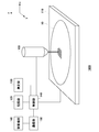
- FIG. 1 The structural example of the electron beam irradiation apparatus 1000 which concerns on this embodiment is shown with the target object 10.
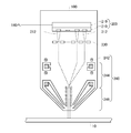
- FIG. The structural example of the electron beam irradiation part 100 which concerns on this embodiment is shown with the target object 10.
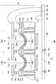
- FIG. The structural example of the surface electron beam source 200 which concerns on this embodiment is shown. 2 shows a control unit 140 and a plurality of drive circuits 220a to 220d according to the present embodiment. A group of a plurality of drive circuits 220 according to the present embodiment is shown (only a quarter portion of an electron source array divided into concentric blocks is displayed). The structure of the drive circuit 220 which concerns on this embodiment is shown. The structure of the 2nd level shifter 290 which concerns on this embodiment is shown.
- Each signal waveform of the drive circuit 220 which concerns on this embodiment is shown.
- Each signal waveform of the drive circuit 220 which concerns on this embodiment is shown.
- the structure of the drive circuit 220 which concerns on the modification of this embodiment is shown.
- FIG. 1 shows a configuration example of an electron beam irradiation apparatus 1000 according to this embodiment together with an object 10.
- the electron beam irradiation apparatus 1000 irradiates the object 10 with a drawing pattern using a plurality of electron beams, and draws a fine pattern on the object 10.
- the object 10 may be a semiconductor substrate, for example, a plate-like substrate formed by processing a crystal of a semiconductor material such as silicon, silicon carbide, germanium, gallium arsenide, gallium nitride, gallium phosphide, or indium phosphide. It's okay.
- the object 10 may be coated with an electron beam resist.
- the electron beam irradiation apparatus 1000 includes an electron beam irradiation unit 100, a stage unit 110, a storage unit 120, a measurement unit 130, a control unit 140, a communication unit 150, and a computer unit 160.
- the electron beam irradiation unit 100 is an electron column that irradiates a plurality of electron beams.
- the electron beam irradiation unit 100 draws a predetermined drawing pattern by irradiating the surface of the object 10 with a plurality of electron beams. Details of the electron beam irradiation unit 100 will be described later.
- the stage unit 110 places an object 10 to be irradiated with an electron beam.
- the stage unit 110 moves the mounted object 10 in the horizontal direction, and causes the electron beam irradiation unit 100 to draw a predetermined fine pattern on one surface of the object 10 at a predetermined position.
- the stage unit 110 includes, for example, an XY stage that moves on a horizontal plane of the stage.
- the stage unit 110 may include a ⁇ stage that rotates around a predetermined rotation axis.
- the stage unit 110 may further include a tilt stage that adjusts the horizontal position of the stage.
- the stage unit 110 may further include a Z stage that moves the object 10 in the vertical direction and adjusts the distance between the object 10 and the electron beam irradiation unit 100.
- the storage unit 120 stores drawing pattern data drawn by the electron beam irradiation unit 100.
- the drawing pattern data may include information such as position data on one surface of the object 10 and irradiation data indicating whether or not to irradiate an electron beam.
- the storage unit 120 may store predetermined drawing pattern data in advance.
- the measuring unit 130 measures the intensity of each of the plurality of electron beams of the electron beam irradiation unit 100. For example, the measurement unit 130 causes the electron beam irradiation unit 100 to individually output an electron beam and measures the intensity of the output electron beam. The measurement unit 130 supplies the measurement result of the electron beam intensity to the control unit 140.
- the control unit 140 is connected to the electron beam irradiation unit 100, the stage unit 110, the storage unit 120, the measurement unit 130, and the communication unit 150, and according to the drawing pattern data stored in the storage unit 120, the electron beam irradiation unit 100 electron beam irradiation and operation of the stage unit 110 are controlled.
- control unit 140 controls the electron beam irradiation of the electron beam irradiation unit 100 by transmitting irradiation data of a plurality of electron beams stored in the storage unit 120 to the electron beam irradiation unit 100. Further, the control unit 140 controls the operation of the stage unit 110 by transmitting a control signal for moving the stage unit 110 to the stage unit 110 in accordance with the drawing pattern data stored in the storage unit 120. Further, the control unit 140 may transmit a control signal to the electron beam irradiation unit 100 and / or the stage unit 110 in accordance with an instruction signal received via the communication unit 150.
- control unit 140 adjusts the output times of the plurality of electron beams output from the electron beam irradiation unit 100 based on the measurement result of the measurement unit 130. For example, the control unit 140 determines the output time of each electron beam based on the measurement results of the intensity of the plurality of electron beams, and supplies a set value including the output time to the electron beam irradiation unit 100.
- the communication unit 150 connects the control unit 140 and the computer unit 160.
- the communication unit 150 may have a general-purpose or dedicated interface, and the control unit 140 and the computer unit 160 may be connected to communicate with each other.
- the communication unit 150 may use a general-purpose high-speed serial interface such as Ethernet (registered trademark), USB, Serial RapidIO, or a parallel interface. Further, the communication unit 150 may connect the control unit 140 and the computer unit 160 wirelessly.
- the computer unit 160 transmits an instruction signal for operating the electron beam irradiation unit 100 and / or the stage unit 110 to the control unit 140.
- the computer unit 160 may execute an operation program for operating the electron beam irradiation apparatus 1000 and transmit an instruction signal according to the operation program.
- the computer unit 160 may have an input device for inputting a user instruction, and may transmit an instruction signal according to the user instruction.
- the computer unit 160 may be a personal computer or a server machine.
- FIG. 2 shows a configuration example of the electron beam irradiation unit 100 according to this embodiment together with the object 10.
- FIG. 2 shows a configuration example of a vertical section of the electron beam irradiation unit 100.
- the electron beam irradiation unit 100 includes a surface electron beam source 200, an acceleration electrode 230, and an electron lens 240.
- the surface electron beam source 200 includes an electron beam generating device 210 and a driving device 219.
- the electron beam generation device 210 is bonded to the drive device 219 and has a plurality of electron beam generation sources 212 that output a plurality of electron beams on the opposite side of the drive device 219.
- a constant voltage is applied to the electron beam of the electron beam generating device 210. For example, approximately ⁇ 5 kV is applied. Details of the electron beam generating device 210 will be described later.
- the driving device 219 is bonded to the side opposite to the electron beam generation source 212 of the electron beam generation device 210 including the plurality of electron beam generation sources 212, and outputs the electron beams from the plurality of electron beam generation sources 212.
- the drive device 219 receives irradiation data from the control unit 140 and causes the plurality of electron beam generation sources 212 to output electron beams according to the irradiation data.
- the driving device 219 may be formed of a semiconductor substrate such as silicon.
- the driving device 219 has a coefficient of thermal expansion of the electron beam generating device 210 to such an extent that the electron beam generating device 210 or the driving device 219 does not bend or peel even when the surface electron beam source 200 is driven and the temperature rises. It may be formed of a material having substantially the same or similar thermal expansion coefficient.
- the acceleration electrode 230 is provided on the side of the surface electron beam source 200 that outputs the electron beam, and a voltage higher than that of the electrode that outputs the electron beam of the surface electron beam source 200 is applied to accelerate the electron beam.
- the acceleration electrode 230 is formed with a plurality of through holes respectively corresponding to the plurality of electron beam generation sources 212, and allows the plurality of electron beams to pass therethrough.
- the acceleration electrode 230 may have a plurality of through holes arranged in a matrix. A constant voltage is applied to the acceleration electrode 230, and as an example, approximately 0 V is applied together with the object 10.
- the electron lens 240 irradiates the object 10 which is the object with a drawing pattern of a plurality of electron beams output from the surface electron beam source 200 at a predetermined magnification. For example, the electron lens 240 reduces the drawing pattern drawn by a plurality of electron beams to 1/100 or less.
- the electron lens 240 has a coil part 242, a lens part 244, and a converging part 246.
- the coil unit 242 controls the deflection of the plurality of electron beams in the XY directions. That is, the coil unit 242 controls the beam shape of the electron beam on the surface of the object 10 irradiated with the electron beam.
- the coil unit 242 may be a rotation coil that corrects the correspondence between the X axis or Y axis of the electron beam irradiation unit 100 and the X axis or Y axis on the surface of the object 10.
- the coil unit 242 may correct the amplitudes of the beam diameter on the surface of the object 10 in the X and Y directions.
- the lens unit 244 images a plurality of electron beams on the surface of the object 10.
- the lens unit 244 may constitute a telecentric lens system and functions as an objective lens of the surface electron beam source 200.
- the converging unit 246 applies an acceleration electric field and / or a deceleration electric field to a plurality of electron beams.
- the converging unit 246 narrows and converges the thicknesses and bundles of a plurality of electron beams, and irradiates the object 10 that is the object with an electron beam having a predetermined energy.
- the electron beam irradiation unit 100 includes the surface electron beam source 200 that generates a plurality of electron beams such as a surface electron beam source, and irradiates the sample with a plurality of electron beams from one electron column. Improve throughput. Conventionally, it has been difficult to manufacture such an electron beam source that generates a plurality of electron beams. However, the surface electron beam source 200 according to the present embodiment is easily manufactured by a manufacturing process such as a semiconductor manufacturing process. can do.
- FIG. 3 shows a configuration example of the surface electron beam source 200 according to the present embodiment.
- the surface electron beam source 200 accelerates and focuses the electrons emitted from each of the plurality of electron beam generation sources 212 and outputs the electrons as a plurality of electron beams.
- the planar electron beam source 200 includes an electron beam generating device 210 and a driving device 219 as described with reference to FIG.
- the surface electron beam source 200 may include a voltage supply unit 202 that supplies a power supply voltage and a signal voltage from the control unit 140 to each unit.
- the first electrode unit 310 is connected via the barrier unit 330.
- the voltage supply unit 202 includes a constant voltage generation circuit and / or a constant current generation circuit and a plurality of electrode units 204, and supplies a power supply voltage and the like to connection destinations connected to the electrode units 204, respectively.
- the voltage supply unit 202 is provided on the surface of the driving device 219 opposite to the electron beam generating device 210 side.
- the plurality of electrode portions 204 may be connected to a plurality of connection destinations by wire bonding or the like.
- electrodes such as the electrode portion 204 described in this embodiment are made of nickel, gold, chromium, titanium, aluminum, tungsten, palladium, rhodium, platinum, copper, ruthenium, indium, iridium, osmium, and / or molybdenum. May include.
- the electrode may be an alloy of two or more materials including these materials.
- the electron beam generating device 210 has a substrate 211 made of a semiconductor crystal such as silicon.
- the substrate 211 is provided with a plurality of recesses 214, an isolation part 340, and a third electrode part 350.
- Each of the plurality of recesses 214 has a concave surface, and a plurality of electron beam generation sources 212a and 212b are formed in each.
- each of the plurality of recesses 214 may be formed in a spherical shape or a parabolic shape.
- Each of the plurality of recesses 214 is formed by, for example, isotropic etching, and electron beam generation sources 212a and 212b that generate an electron beam are formed.
- the plurality of recesses 214 are formed by wet etching.
- the electron beam generation source 212 includes a polysilicon layer 216, a first insulating film 215, a second insulating film 218, an electron emission unit 300, a first electrode unit 310, a second electrode unit 320, and a barrier unit 330. Including.
- the polysilicon layer 216 is formed on the surface of the substrate 211 where the plurality of recesses 214 are formed. At least a part of the polysilicon layer 216 formed in the recess 214 becomes an electron-emitting portion 300 that is anodically activated and nanocrystallized.
- the first insulating film 215 and the second insulating film 218 are formed on the surface of the substrate 211 on which the polysilicon layer 216 is formed.
- the first insulating film 215 and the second insulating film 218 electrically insulate the polysilicon layer 216 of the adjacent electron beam generation source 212 and prevent a leakage current from being generated through the polysilicon layer 216.
- the first insulating film 215 is a SiO 2 film formed by thermal oxidation
- the second insulating film 218 is a SiN film formed by a CVD method or the like.
- the electron emission unit 300 is provided in each of the plurality of recesses 214 and emits electrons.
- the plurality of recesses that is, the plurality of electron emission units 300 are arranged in a matrix on one surface of the substrate 211 and emit electrons according to the drive voltage from the drive device 219.
- each of the plurality of electron emission units 300 includes a nanocrystal.
- the electron emission unit 300 is formed of nanocrystalline silicon. Nanocrystalline silicon forms a surface oxide film that functions as an electron tunneling barrier, and a plurality of nanocrystalline silicons are arranged to form a column connecting the electron tunneling barriers.
- the electron emission part 300 can control the amount of electron emission precisely and with good reproducibility by having a nanocrystal.
- the electron emission unit 300 when the electron emission unit 300 is formed of nanowires in which a plurality of such nanocrystalline silicons are arranged, the nanowires are not formed perpendicular to the surface that outputs electrons, and the output surface depends on the crystal orientation. May be tilted with respect to the normal. In this case, the electron emission unit 300 may output electrons in a direction different from the normal direction of the output surface. In this case, the electron emission unit 300 determines the electron emission amount by multiplying the distribution of the tunnel probability in a different direction with respect to the normal of the output surface and the distribution in which the nanowire emits electrons in the direction.
- the electron emission unit 300 includes the concave portion 214, it is possible to output more electrons as an effective electron beam to the outside as compared with the amount of electron emission when the concave shape is flat.
- the electron emission part 300 is formed in a flat shape by forming a direction in which the electron emission distribution is higher and / or a direction in which the tunnel probability distribution is higher in the direction in which the electron beam is output. More electrons can be output as an electron beam than the amount of emitted electrons.
- the shape of the recess 214 is such that the direction in which electrons are emitted from the plurality of electron emission units 300 and the direction in which multiplication of the tunnel probability of electrons in that direction becomes larger is the corresponding opening of the first electrode unit 310.
- each of the plurality of electron emission units 300 may include an insulating film that tunnels emitted electrons instead of the nanocrystal. Since such an insulating film can be adjusted by the probability of tunneling the amount of electrons emitted, the amount of electrons emitted can be controlled by the material, film thickness, and voltage applied to the insulating film. it can.
- the first electrode unit 310 is provided corresponding to each of the plurality of electron emission units 300, accelerates the electrons emitted by the corresponding electron emission unit 300, and forms an electron beam from the recess 214 provided in the electron emission unit 300. Output.
- Each of the plurality of first electrode portions 310 has an opening 312 and is formed in a plate shape on one surface of the substrate 211 where the plurality of recesses 214 are provided, and from the opening 312 due to a potential difference with the corresponding recess 214.
- the electron beam is focused and output.
- the opening 312 is formed near the center of the first electrode unit 310 and / or the electron emission unit 300.
- the opening 312 may be a circular through hole.
- the first electrode part 310a is provided corresponding to the electron emission part 300a, and shows an example in which electrons emitted from the electron emission part 300a are accelerated and output as an electron beam from the opening 312a.
- the 1st electrode part 310b is provided corresponding to the electron emission part 300b, and accelerates the electron which the electron emission part 300b discharge
- the plurality of first electrode portions 310 (the first electrode portion 310a and the first electrode portion 310b in the example in the figure) are electrically connected, and a predetermined constant voltage is applied thereto.
- the first electrode unit 310 may be electrically connected to an electrode provided outside the substrate 211 and may have a connection unit to which a drive voltage or the like from the control unit 140 is applied.
- the connection part may be an electrode part in which a conductive material is further formed on a part of the first electrode part by plating or the like.
- the connecting portion may be connected to an external electrode by wire bonding or the like.
- the second electrode portion 320 is provided in each of the plurality of recesses 214 and is formed of a conductive material that covers the recesses 214.
- the second electrode unit 320 causes the electrons emitted from the electron emission unit 300 to be output as an electron beam from the opening 312 due to a potential difference from the first electrode unit 310.
- the second electrode unit 320 is formed to be thin enough to pass electrons emitted from the electron emission unit 300.
- the plurality of second electrode portions 320 provided in the plurality of recesses 214 are electrically connected, and a predetermined constant voltage is applied thereto.
- the first electrode unit 310 and the second electrode unit 320 may be applied with a driving voltage at which the potential difference between these electrodes is several tens to several hundreds V, respectively.
- the first electrode unit 310 and the second electrode unit 320 are each applied with a driving voltage having a potential difference of several hundreds of volts from the control unit 140.
- the first electrode part 310 and the second electrode part 320 are each applied with a driving voltage with a potential difference of 150V.
- the second electrode part 320 includes a connection part 322.
- connection part 322 is an electrode part formed to be thicker in the second electrode part 320, and is electrically connected to an electrode provided outside the substrate 211, and applied with a driving voltage.
- the connection part 322 may be an electrode part in which a conductive material is further formed on a part of the second electrode part by plating or the like.
- the connection portion 322 may be connected to an external electrode by wire bonding or the like.
- the barrier portion 330 is provided at a position corresponding to the plurality of recesses 214 between the plurality of first electrode portions 310 and the substrate 211, and is formed of an insulating material.
- the barrier unit 330 separates a predetermined distance between the substrate 211 and the first electrode unit 310 and supports the first electrode unit 310 while electrically connecting the first electrode unit 310 and the second electrode unit 320. Insulate.
- the barrier portion 330 may be formed of a resin or the like, and may instead be a silicon oxide film formed by a CVD method or the like.
- the electron beam generation source 212 described above applies electrons from the opening 312 by applying an electric field generated by a driving voltage applied to each of the first electrode unit 310 and the second electrode unit 320 to electrons emitted from the electron emission unit 300. Generate a beam.
- the concave portion 214 is formed in a concave shape, a spherical shape, or a parabolic shape, so that the electron emission surface of the electron emission unit 300 is also concave, spherical, or It is formed in a parabolic shape.
- the electron beam generation source 212 can easily focus the electron emitting unit 300 on the opening 312 by aligning the direction in which the electron emitting unit 300 emits electrons with the direction of the opening 312. That is, the electron beam generation source 212 can increase the number of electrons focused on the opening 312 and increase the density of the generated electron beam.
- the electron beam generation source 212 irradiates the object 10 with the generated electron beam through the subsequent electron lens 240.
- the electron lens 240 may have an aberration that causes blurring, distortion, or the like in the image formation of the electron beam, similar to an optical lens or the like.
- the electron lens 240 may shorten the focal position of electrons traveling near the outside of the beam compared to electrons traveling near the center of the electron beam to be imaged.
- the electron beam generation source 212 may correct the aberration while increasing the electron beam density by forming the electron emitting surface of the electron emitting unit 300 into a concave shape, a spherical shape, or a parabolic shape. .
- the electron beam generation source 212 makes the recess 214 flat, the electrons output from the region where the normal direction of the electron emission surface of the electron emission unit 300 is in the vicinity of the opening 312 are in the center of the electron beam. Easy to focus.
- the electron emission unit 300 is directed to a region near the edge side of the emission surface with a distance between the region near the center of the emission surface and the opening 312 while directing the electron emission surface toward the opening 312.
- a surface for shortening the distance from the opening 312 is formed. That is, by forming the emission surface so that electrons that are likely to be focused outside the electron beam reach the opening 312 more quickly, the focal length of the electrons is increased. This is equivalent to the fact that the concave portion 214 concentrates the laminar flow of electrons emitted from a portion closer to the center point of the emission surface of the electron emission unit 300 to a position closer to the center point to generate negative aberration. .
- the electron beam generation source 212 causes electrons traveling in the vicinity of the center of the electron beam to be generated (for example, in the vicinity of a perpendicular passing through the approximate center of the recess 214 indicated by AA ′ and BB ′ in FIG. 3).
- the focal length of electrons traveling near the outside of the electron beam can be increased.
- the electron beam generating source 212 increases the focal length of the electron beam as it moves away from the center of the optical axis of the electron beam, and concentrically distributes the focal length in a cross section perpendicular to the irradiation direction of the electron beam.
- the electron beam generation source 212 can correct the aberration of the electron lens 240 by forming an emission surface corresponding to the aberration of the electron lens 240.
- the region near the edge side of the emission surface of the electron emission unit 300 is closer to the outside of the electron beam generation source 212 than the region near the center, and thus is easily affected by an external electric field. That is, electrons output from the region near the edge side of the emission surface are likely to be output in a direction inclined from the normal line of the emission surface, and the focal length tends to be long.
- the electron beam generation source 212 forms a distribution of focal lengths in the electron beam to be output depending on the external electric field. Therefore, the shape of the emission surface of the electron emission unit 300 is adjusted according to such distribution. Then, the aberration of the electron beam imaged on the object 10 may be corrected.
- the second electrode portion 320 forms an electrode that covers the recess 214, and keeps the recess 214 at the same potential. Accordingly, the second electrode unit 320 can reduce the influence of the external electric field while emitting electrons with a stable velocity distribution from the electron emission unit 300 and focusing the electrons in the vicinity of the opening 312.
- the isolation part 340 is formed by being filled with an insulating material.
- the isolation unit 340 is formed so as to surround each of the plurality of electron beam generation sources 212 and electrically isolates the electron beam generation sources 212 from each other.
- the isolation part 340 is a groove formed in a plurality of rings or lattices corresponding to the plurality of electron emission parts 300 on the surface of the substrate 211 opposite to the surface on which the plurality of recesses 214 are formed. Is filled with an insulating material such as resin.
- the third electrode portion 350 is formed on the lower surface of the substrate 211 opposite to the upper surface on which the plurality of recesses 214 are formed, corresponding to each of the plurality of electron emission portions 300.
- the third electrode unit 350 is applied with a driving voltage for emitting electrons from the plurality of electron emission units 300.
- the third electrode unit 350 may include a conductive film 352 formed on the lower surface of the substrate 211.
- the third electrode unit 350 is electrically connected to the driving device 219.
- the driving device 219 includes a plurality of driving circuits 220a and 220b corresponding to the plurality of electron beam generation sources 212a and 212b, respectively.
- the drive circuits 220a and 212b supply a drive voltage for driving each of the plurality of electron beam generation sources 212.
- the drive circuit 220 individually supplies a drive voltage for emitting electrons from the plurality of electron emission units 300 to each of the plurality of electron emission units 300.
- the driver circuit 220a and the like may be formed over a semiconductor substrate, and one surface of the semiconductor substrate may be attached to the substrate 211.
- the drive circuit 220 has a plurality of electrode portions 222 corresponding to the third electrode portions 350 formed on the substrate 211, and the electrode portions 222 are electrically connected to the corresponding third electrode portions 350 while being connected to the substrate. 211, and a driving voltage is supplied through the electrode unit 222.
- the electrode portions 222 are formed at the same pitch as the third electrode portions 350 so as to correspond to the third electrode portions 350 formed on the substrate 211 at a pitch of about 100 ⁇ m.
- the drive circuit 220 may be electrically connected to an external electrode or the like, and may have a plurality of connection portions 224 to which a drive voltage, a power supply voltage, and the like are applied.
- the connection portion 224 may be connected to an external electrode by wire bonding or the like.
- At least one of the plurality of drive circuits 220 may include an inspection terminal 354 that is exposed to the outside via the voltage supply unit 202 and outputs a drive voltage.
- the inspection terminal 354 outputs a drive signal supplied from the drive circuit 220 to the corresponding electron beam generation source 212 to the surface of the drive device 219 opposite to the electron beam generation device 210 at the time of inspection.
- the drive circuit 220 may further apply a different offset bias depending on the arrangement of each of the plurality of electron emission units 300.
- the plurality of electron emission units 300 are individually applied with a driving voltage to emit electrons, and the corresponding plurality of electron beam generation sources 212 generate a plurality of electron beams.
- the plurality of electron beam generation sources 212a and the like cause the generated plurality of electron beams to be imaged by the subsequent electron lens 240 and irradiate the object 10 with a drawing pattern.
- the optical system such as the electron lens 240 gives a slight difference in focal position between the electron beam passing near the center of the lens and the electron beam passing near the outer edge of the lens, and blurs the drawn image by a plurality of electron beams. May cause distortion and the like.
- the electron lens 240 may shorten the focal position with respect to an electron beam passing near the outer edge of the lens as compared with an electron beam passing near the center of the lens.
- the drive circuit 220 has a function of generating an electron beam that passes near the outer edge of the electron lens 240 as compared with the electron beam source 212 that generates an electron beam passing near the center of the electron lens 240. Supply high offset voltage.
- the drive circuit 220 increases the output speed of the electron beam that passes through the vicinity of the outer edge of the electronic lens 240 to increase the focal length, and cancels the focal position that is shortened by the electronic lens 240 to correct the correction. it can.
- the plurality of electron emission units 300 may be distributed to a plurality of blocks according to their arrangement, and the drive circuit 220 may apply an offset bias for each block.
- the plurality of electron emission units 300 that are arranged in the vicinity of the center on one surface of the substrate 211 and emit an electron beam that passes through the vicinity of the center of the electron lens 240 are the same.
- the other electron emission units 300 may be distributed to two or more blocks in a substantially concentric manner around the central block.
- the plurality of electron emission units 300 are divided into two or more concentrically in the outer edge direction of the electron lens 240 with the electron emission unit 300 that outputs an electron beam passing near the center of the electron lens 240 as a central block.
- the electron emission unit 300 corresponding to the annular region is distributed as another block.
- the drive circuit 220 adjusts the focal position of the electron beam for each region divided concentrically around the electron beam passing near the center of the electron lens 240 by applying different offset bias for each block.
- the drive circuit 220 applies a negative voltage of several kV to several tens of kV to the first electrode unit 310 and the second electrode unit 320.
- the drive circuit 220 applies ⁇ 5 kV to the second electrode unit 320 corresponding to the electron emission unit 300 distributed in the center of the concentric circle, and ⁇ 5 kV + 150 V to the corresponding first electrode unit 310.
- the electron beam generation source 212 generates an electron beam by applying an electric field generated by a potential difference of 150 V to electrons emitted from the electron emission unit 300, and the generated electron beam is generated with a potential difference of about 5 kV from the acceleration electrode 230. Accelerate.
- the driving circuit 220 applies ⁇ 5 kV + nV to the corresponding second electrode portion and ⁇ 5 kV + 150 V + nV to the corresponding first electrode portion every n blocks different from the central block toward the outer edge.
- the drive circuit 220 may finely adjust the acceleration electric field of the electron beam for each block by changing the drive voltage by about 1 V every time the block is different.
- the above-described surface electron beam source 200 has a plurality of electron beam generation sources 212 and can individually drive the plurality of electron beam generation sources 212 to output a plurality of electron beams. . Accordingly, the electron beam irradiation unit 100 including the surface electron beam source 200 can irradiate the object with a predetermined drawing pattern by a plurality of electron beams.
- the electron beam generation source 212 is formed in each of the plurality of recesses 214 formed on the semiconductor substrate by a simple method such as isotropic etching. Therefore, the plurality of electron beam generation sources 212 can be formed on the substrate 211 by a semiconductor manufacturing process or the like. That is, for example, the electron beam generation sources 212 are formed in an area of 1 cm ⁇ 1 cm of the substrate 211 and arranged in a matrix of 100 ⁇ 100. As described above, the electron beam generation source 212 is formed in a matrix shape with a pitch of about 100 ⁇ m, so that the object can be irradiated with a drawing pattern with a pitch of about 1 ⁇ m or less by the electron lens 240.
- the electron beam generation source 212 provided in the surface electron beam source 200 includes a plurality of recesses 214 and a barrier portion 330 formed by a separate process at a position corresponding to the plurality of recesses 214. Accordingly, the surface electron beam source 200 can generate a plurality of electron beams without precisely forming a cylindrical hole having a bottom having a predetermined shape such as a concave shape, a spherical shape, or a parabolic shape. The source 212 can be easily formed. Thus, the surface electron beam source 200 can include a plurality of electron beam generation sources 212 formed with a small area and a high density. Therefore, the electron beam irradiation unit 100 can irradiate about 10000 electron beams while reducing the size of the apparatus.
- the surface electron beam source 200 and the electron beam irradiation unit 100 may be provided in a device using an electron beam, such as an electron microscope, an electron beam microanalyzer, a cathode ray tube, a transmission tube, an imaging tube, a vacuum tube, a processing device, a heating device. You may use for an apparatus or a sterilizer.
- an electron beam such as an electron microscope, an electron beam microanalyzer, a cathode ray tube, a transmission tube, an imaging tube, a vacuum tube, a processing device, a heating device. You may use for an apparatus or a sterilizer.
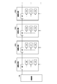
- FIG. 4 shows the control unit 140 and a plurality of drive circuits 220a to 220d.
- the plurality of drive circuits 220a to 220d are cascade-connected to the control unit 140, and data is transmitted by propagating data from the control unit 140 in the order of the drive circuit 220a, the drive circuit 220b, the drive circuit 220c, and the drive circuit 220d. Is transmitted.
- the control unit 140 sequentially outputs irradiation data to the plurality of drive circuits 220a to 220d cascaded in series, and causes the plurality of drive circuits a to d to write the irradiation data. Further, the control unit 140 sequentially outputs a set value of the electron beam output time to the plurality of drive circuits 220a to 220d, and sets the set value for each of the plurality of drive circuits 220a to 220d.
- control unit 140 sequentially transmits the irradiation data to the shift register SR of the drive circuit 220a and shifts the irradiation data between the shift registers, whereby a plurality of shift registers SR of the plurality of drive circuits 220a to 220d are transferred.
- Irradiation data for the electron beam generation sources 212a to 212d corresponding to the drive circuits 220a to 220d of the first and second driving circuits 220a to 220d are stored.
- the control unit 140 stores irradiation data in the register LT0 of the plurality of drive circuits 220a to 220d by transmitting a command to store the value of the shift register SR in the register LT0 to the plurality of drive circuits 220a to 220d.
- the controller 140 stores the set value of the output time of the electron beam generation source 212 corresponding to each of the drive circuits 220a to 220d in the registers LT1 and LT2 of the plurality of drive circuits 220a to 220d by the same method.
- each of the drive circuits 220a to 220d stores a 2-bit (four-stage) value as a set value for the output time.
- the irradiation data register of the drive circuits 220a to 220d may be 2 bits or more, and the set value register may be 3 bits or more or 1 bit.
- FIG. 5 shows a group of a plurality of drive circuits 220 (only a quarter of the electron source array divided into concentric blocks is displayed).
- the plurality of drive circuits 220 may be divided into a plurality of groups, and the drive circuits 220 may be connected in cascade for each group.
- the area of the surface electron beam source 200 is divided by a block surrounded by a plurality of concentric circles for each focal length of the electron beam.
- one block surrounded by concentric circles is divided into a plurality of groups G1, G2, etc.
- the plurality of drive circuits 220 are connected in cascade for each group, and the control unit 140 sequentially outputs irradiation data and the like to the plurality of drive circuits 220 included in each of the plurality of groups as indicated by arrows. Thus, the data is written in the plurality of drive circuits 220.
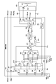
- FIG. 6 shows the configuration of the drive circuit 220.
- the drive circuit 220 supplies a drive voltage to the corresponding electron beam generation source 212 based on the irradiation data written from the control unit 140 and the set value of the output time.
- the drive circuit 220 includes a shift register SR, a register LT0, a register LT1, a register LT2, a buffer amplifier 248, an AND circuit 250, an AND circuit 252, an AND circuit 254, an AND circuit 260, an AND circuit 262, an AND circuit 264, an AND circuit 266,
- the circuit includes an OR circuit 268, an AND circuit 270, an AND circuit 272, an OR circuit 274, a first level shifter 280, and a second level shifter 290.
- the driving circuit 220 receives the clock signal SRckin and the data signal SRdin from the control unit 140, and supplies the clock signal SRckin and the data signal SRdin to the subsequent driving circuit 220.
- the subsequent drive circuit 220 receives the clock signal SRckin and the data signal SRdin from the previously connected drive circuit 220 and supplies them to the subsequent drive circuit 220.
- the driving circuit 220 receives a plurality of enable signals Ena0 to 3 having a predetermined length of rising period, a register specifying signal Md0, a register specifying signal Md1, a write signal Wr, a disable signal Dis, A reset signal Rst is input. These signals may be connected to the control unit 140 in a one-to-many manner, or may be connected in cascade to the control unit 140 instead.
- the buffer amplifier 248 receives a clock signal from the control unit 140 or the driving circuit 220 connected in front, amplifies the clock signal, and supplies the amplified clock signal to the driving circuit 220 connected later.
- the control unit 140 or the shift register of the driving circuit 220 connected before is connected to the data input D
- the shift register of the subsequent driving circuit 220 is connected to the data output Q
- the control unit is connected to the reset input R. 140 is connected.
- the shift register SR inputs the data signal SRdin from the control unit 140 or the previously connected driving circuit 220 to the data input D, and takes in the data signal SRdin at a timing (for example, a rising timing) indicated by the clock signal SRckin. Then, the shift register SR outputs the captured data signal SRdin to the register LT0, the register LT1, the register LT2, and the drive circuit 220 connected later.
- the shift register SR receives a reset signal Rst from the control unit 140.
- the AND circuit 250 inputs the inverted value of the register specifying signal Md0, the inverted value of the register specifying signal Md1, and the write signal Wr, and outputs a logical product of these to the register LT0.
- the AND circuit 252 receives the register designation signal Md0, the inverted value of the register designation signal Md1, and the write signal Wr, and outputs a logical product of these to the register LT1.
- the AND circuit 254 receives the inverted value of the register designation signal Md0, the register designation signal Md1, and the write signal Wr, and outputs a logical product of these to the register LT2.
- the output Q of the shift register SR is connected to the data input D, and the output of the AND circuit 250 is connected to the clock input E.
- the register LT0 receives the output of the AND circuit 250 as an enable signal, and stores the output value of the shift register SR in a state where the output from the AND circuit 250 rises. Thereby, the register LT0 stores the output of the shift register SR when the write signal Wr rises in a state where the control unit 140 outputs the L-level register designation signal Md0 and outputs the L-level register designation signal Md1.
- the register LT0 is connected to the reset input R to the control unit 140, and receives the reset signal Rst from the control unit 140.
- the register LT0 outputs the values stored in the AND circuit 260, the AND circuit 262, the AND circuit 264, and the AND circuit 266.
- the output Q of the shift register SR is connected to the data input D, and the output of the AND circuit 252 is connected to the clock input E.
- the register LT1 stores the output value of the shift register SR with the output from the AND circuit 252 rising. As a result, the register LT1 stores the output of the shift register SR when the write signal Wr rises in a state where the control unit 140 outputs the H-level register designation signal Md0 and the L-level register designation signal Md1. .
- the register LT1 is connected to the reset input R and the control unit 140 is input with the reset signal Rst from the control unit 140.
- the register LT1 outputs the values stored in the AND circuit 260, the AND circuit 262, the AND circuit 264, and the AND circuit 266.
- the output Q of the shift register SR is connected to the data input D, and the output of the AND circuit 254 is connected to the clock input E.
- the register LT2 stores the output value of the shift register SR with the output from the AND circuit 254 rising. As a result, the register LT2 stores the output of the shift register SR when the write signal Wr rises in a state where the control unit 140 outputs the L-level register designation signal Md0 and the H-level register designation signal Md1.
- control unit 140 is connected to the reset input R of the register LT2, and the reset signal Rst is input from the control unit 140.
- the register LT2 outputs the values stored in the AND circuit 260, the AND circuit 262, the AND circuit 264, and the AND circuit 266.
- the AND circuit 260 inputs the inverted value of the output of the register LT1, the inverted value of the output of the register LT2, and the enable signal Ena0 from the control unit 140, and outputs a logical product of these to the OR circuit 268. That is, when the value stored in the register LT1 is 0 and the value stored in the register LT2 is 0, the AND circuit 260 outputs an H level signal to the OR circuit 268 corresponding to the rising period of the enable signal Ena0.
- the AND circuit 262 receives the output of the register LT1, the inverted value of the output of the register LT2, and the enable signal Ena1 from the control unit 140, and outputs a logical product of these to the OR circuit 268. That is, when the value stored in the register LT1 is 1 and the value stored in the register LT2 is 0, the AND circuit 262 outputs an H level signal to the OR circuit 268 corresponding to the rising period of the enable signal Ena1.
- the AND circuit 264 receives the inverted value of the output of the register LT1, the output of the register LT2, and the enable signal Ena2 from the control unit 140, and outputs a logical product of these to the OR circuit 268. That is, when the value stored in the register LT1 is 0 and the value stored in the register LT2 is 1, the AND circuit 264 outputs an H level signal to the OR circuit 268 corresponding to the rising period of the enable signal Ena2.
- the AND circuit 266 inputs the output of the register LT1, the output of the register LT2, and the enable signal Ena3 from the control unit 140, and outputs a logical product of these to the OR circuit 268. That is, when the value stored in the register LT1 is 1 and the value stored in the register LT2 is 1, the AND circuit 266 outputs an H level signal to the OR circuit 268 corresponding to the rising period of the enable signal Ena3.
- the OR circuit 268 receives outputs from the AND circuit 260, the AND circuit 262, the AND circuit 264, and the AND circuit 266, and outputs a logical sum of these inputs to the AND circuit 270. As a result, the OR circuit 268 outputs an H level signal corresponding to the rising period of any one of the enable signals Ena0 to Ena3.
- the AND circuit 270 inputs the outputs of the register LT0 and the OR circuit 268, and outputs a logical product of these to the first level shifter 280 as an enable signal Ena. That is, when 1 is stored in LT0, AND circuit 270 outputs an H level signal corresponding to one rising period of enable signals Ena0 to Ena3.
- the AND circuit 272 receives the inverted value of the register LT0 and the disable signal Dis from the control unit 140, and outputs a logical product of these to the OR circuit 274.
- the OR circuit 274 receives the reset signal Rst from the AND circuit 272 and the control unit 140, and inputs the logical sum of these to the first level shifter 280 as a disable signal.
- the first level shifter 280 is connected to the AND circuit 270, the OR circuit 274, and the second level shifter 290, receives the enable signal Ena from the AND circuit 270, and receives the disable signal Dis from the OR circuit 274. After converting the voltage level, the corresponding enable signal Ena-i and disable signal Dis-i are output to the second level shifter 290.
- the first level shifter 280 outputs a 5V enable signal Ena-i in response to receiving an enable signal Ena having an H level of 1.8V, and inputs a disable signal Dis having an H level of 1.8V. In response to this, the 5V disable signal Dis-i is output.
- the second level shifter 290 is connected to the first level shifter 280 and the electron beam generation source 212, receives the precharge signal HVpchg from the control unit 140, receives the enable signal Ena-i from the first level shifter 280, and receives the precharge signal HVpchg. In response to this, a drive voltage higher than the enable signal Ena-i is output to the electron beam generation source 212.
- the second level shifter 290 receives a power supply voltage VH of 20 V and a reference voltage VL of 0 V, and outputs a driving voltage of H level to the electron beam generation source 212 when a precharge signal is input from the precharge signal HVpchg. . Further, the second level shifter 290 outputs an L level drive voltage to the electron beam generation source 212 after the enable signal Ena-i from the first level shifter 280 is input until the precharge signal HVpchg is input again. To do. Further, the second level shifter 290 does not output the L level drive voltage to the electron beam generation source 212 during the period when the disable signal Dis-i is input.
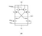
- FIG. 7 shows the configuration of the second level shifter 290.
- the second level shifter 290 receives the power supply voltage VH and the reference voltage VL, receives the precharge signal HVpchg from the controller 140, and receives the enable signal Ena-i and the disable signal Dis-i from the first level shifter 280.
- the drive voltage Vout is supplied to the electron beam generation source 212.
- the second level shifter 290 includes a switch Tr1, a switch Tr2, a switch Tr3, a switch Tr4, a switch Tr5, and a switch Tr6.
- the switch Tr1 may be a semiconductor switch, for example, an NMOS transistor in the present embodiment.
- the switch Tr1 has a gate connected to the first level shifter 280 and inputs an enable signal Ena-i, a drain connected to the switch Tr3 and the drive voltage Vout, and a drain connected to the switches Tr4 and Tr6 via a resistor.
- the source is connected to the reference potential VL.
- the switch Tr2 may be a semiconductor switch, for example, an NMOS transistor in this embodiment.
- the switch Tr2 has a gate connected to the first level shifter 280 and inputs the disable signal Dis-i, a drain connected to the switch Tr4, a drain connected to the switches Tr3 and Tr5 via a resistor, and a source Connected to the reference potential VL.
- the switch Tr3 may be a semiconductor switch, for example, a PMOS transistor in this embodiment.
- the switch Tr3 has a gate connected to the switches Tr2 and Tr4 via resistors, a source connected to the power supply voltage VH, a drain connected to the switch Tr1 and the drive voltage Vout, and a drain connected to the switches Tr2 and Trout via the resistors. Connected to Tr4.
- the switch Tr4 may be a semiconductor switch, for example, a PMOS transistor in this embodiment.
- the switch Tr4 has a gate connected to the switch Tr6, a gate connected to the switches Tr1 and Tr3 via resistors, a source connected to the power supply voltage VH, a drain connected to the switch Tr2, and a drain connected to the resistor Via the switch Tr3 and the switch Tr5.
- the switch Tr5 may be a semiconductor switch, for example, a PMOS transistor in this embodiment.
- the gate is connected to the switch Tr6, the precharge signal HVpchg is input from the control unit 140, the source is connected to the power supply voltage VH, the drain is connected to the switch Tr3, and the drain is further connected to the switch Tr2 via a resistor. And connected to the switch Tr4.
- the switch Tr6 may be a semiconductor switch, for example, a PMOS transistor in the present embodiment.
- the switch Tr6 has a gate connected to the switch Tr5 to form a current mirror circuit with the switch Tr5.
- the switch Tr6 has a gate connected to the control unit 140 and inputs the precharge signal HVpchg from the control unit 140, a source connected to the power supply voltage VH, a drain connected to the switch Tr4, and a drain connected to the resistor. Via the switch Tr1 and the switch Tr3.
- the switches Tr5 and Tr6 are turned off.
- the enable signal Ena-i is input in this state, the switch Tr1 is turned on, and the source side of the switch Tr1 is connected to the reference potential VL via the switch Tr1, so that the gate of the switch Tr4 becomes L level and the switch Tr1 is switched to the switch Tr1.
- Tr4 is turned on.
- the gate of the switch Tr3 is connected to the power supply voltage VH via the switch Tr4, and the switch Tr3 is turned off.
- the drive voltage Vout decreases to the reference potential VL.
- the second level shifter 290 uses the switches Tr1 to Tr4 to drive a high voltage (eg, 20V) drive voltage in response to the rise of the enable signal Ena-i from the low voltage (eg, 5V) control unit 140. Vout is lowered.
- the electron beam generation source 212 outputs an electron beam in response to the fall of the drive voltage Vout.
- the second level shifter 290 disables the output of the drive voltage Vout by the disable signal Dis-i from the control unit 140.
- the second level shifter 290 turns on the switches Tr5 and Tr6 and raises the drive voltage Vout in response to the fall of the precharge signal HVpchg.
- the second level shifter 290 prevents the through current from flowing from the power supply voltage VH to the reference potential VL by controlling on / off of the switches Tr3 and Tr4 by the switches Tr5 and Tr6.
- the irradiation data and the output time of the electron beam are stored in the registers LT0 to LT2 of the drive circuit 220 of the plurality of electron beam generation sources 212.
- an optimal electron beam output time can be set for each electron beam generation source 212, so that the surface electron beam source 200 has an electron for each electron beam generation source 212.
- An electron beam having no variation in emission intensity (current density) can be output, and the object 10 can be irradiated with an electron beam having a uniform dose.
- the surface electron beam source 200 having a variation in the output electron beam can be used for exposure of an object, so that the mass productivity and manufacturing cost of the electron beam irradiation apparatus can be reduced. Can be improved.
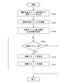
- FIG. 8 shows a processing flow of the electron beam irradiation method according to the present embodiment.
- the electron beam irradiation apparatus 1000 draws a predetermined drawing pattern on the object 10 by executing the processes from S102 to S112.
- the control unit 140 sequentially drives the plurality of electron beam generation sources 212 of the electron beam irradiation unit 100, and causes each electron beam generation source 212 to output an electron beam.
- the control unit 140 may cause each electron beam of the plurality of electron beam generation sources 212 to output an electron beam with the same output time.
- the measurement unit 130 measures the intensity of the electron beam output from each electron beam generation source 212.
- the measurement unit 130 measures the intensity of the electron beam output from the electron beam generation source 212 by the electron beam detector, for example, using a microammeter.
- the measurement unit 130 supplies the measurement result of the electron beam intensity to the control unit 140.
- control unit 140 sets the output time of the electron beam from each electron beam generation source 212 according to the intensity of the electron beam output from the electron beam generation source 212 measured by the measurement unit 130.
- control unit 140 adjusts the electron beam output times of the plurality of electron beams with respect to a predetermined electron beam output time according to the intensities of the plurality of electron beams measured by the measurement unit 130.
- the control unit 140 may set a short electron beam output time for the measured electron beam having a high output intensity and may set a long electron beam output time for an electron beam having a low output intensity.
- the control unit 140 may set an electron beam output time that is inversely proportional to the measured output intensity for each electron beam.
- control unit 140 determines a predetermined electron beam output time based on a drawing pattern irradiated within a predetermined range with respect to an irradiation position where one electron beam is irradiated onto the object 10.
- the difference in the optimum exposure time of each electron beam due to the proximity effect of the drawing pattern is compensated by adjusting the electron beam output time for outputting the one electron beam.
- the control unit 140 applies the predetermined electron beam output time to a predetermined electron beam output time based on a drawing pattern of an adjacent electron beam adjacent to an electron beam whose irradiation position is irradiated to the object 10.
- the electron beam output time for outputting the electron beam may be adjusted.
- the control unit 140 may reduce the electron beam output time of one electron beam as the number of the plurality of electron beams arranged adjacent to each other in a predetermined range is larger.
- control unit 140 includes a drawing pattern irradiated with a single electron beam within a predetermined range with respect to an irradiation position where the object 10 is irradiated, the object 10, and a resist on the object 10.
- the electron beam output time of the one electron beam may be adjusted with respect to a predetermined electron beam output time based on the above-mentioned types.
- the control unit 140 supplies the set value of the adjusted electron beam output time to the plurality of drive circuits 220 of the electron beam irradiation unit 100, and sets the set value of the electron beam output time to the registers LT1 and LT2 of the drive circuit 220. Write.
- control unit 140 determines whether there is drawing pattern data to be drawn in the storage unit 120 or the like. If there is drawing pattern data, the control unit 140 advances the process to S110, and if there is no drawing pattern data, ends the process.
- the control unit 140 supplies irradiation data included in the drawing pattern data to the plurality of drive circuits 220 of the electron beam irradiation unit 100. For example, the control unit 140 writes the irradiation pattern in the register LT0 of the drive circuit 220. Further, the control unit 140 supplies an instruction to the stage unit 110 so that the stage unit 110 drawn by an electron beam moves by one dot.
- the electron beam irradiation unit 100 irradiates the object 10 with the electron beam and draws a drawing pattern on the object 10.
- the drive circuit 220 supplies the reference potential VL to the drive voltage Vout to the electron beam generation source 212 if the value written in the register LT0 is 1, and supplies the drive voltage Vout to the drive voltage Vout if the value is 0. Supply voltage VH.
- the drive circuit 220 supplies the reference potential VL as the drive voltage Vout to the electron beam generation source 212 for a predetermined period according to the enable signals Ena0 to Ena3 selected by the values written in the registers LT1 and LT2. .
- the stage unit 110 sequentially moves the irradiation region of the electron beam on the object 10 by moving the object 10 based on the drawing pattern data.
- the control unit 140 returns the process to S108.
- the electron beam irradiation apparatus 1000 determines the output times of the plurality of electron beam generation sources 212 before drawing the object 10 according to the intensity of the electron beam. Set to the registers LT1 and LT2 of the drive circuit 220.
- the electron beam irradiation apparatus 1000 can output an optimum amount of electron beams for each electron beam generation source 212 and reduce unevenness in the exposure amount due to variations in output intensity of the plurality of electron beam generation sources 212. To do. Therefore, the electron beam irradiation apparatus 1000 can expose the object 10 with high throughput and high accuracy by using a plurality of electron beams.
- FIG. 9 shows signal waveforms of the drive circuit 220 according to the present embodiment in S106 and S110.
- the control unit 140 serially outputs the electron beam output time data a1 to an to n (n is an integer of 1 or more) drive circuits 220 based on the data signal SRdin.
- values corresponding to the data a1 to an are set in the shift registers SR of the n drive circuits 220.
- the control unit 140 raises the register designation signal Md0 output in parallel to each drive circuit 220 to H level, sets the register designation signal Md1 to L level, and applies a rectangular pulse to the write signal Wr.
- the data a1 to an stored in the shift registers SR of the n drive circuits 220 are written to the register LT1 of each drive circuit 220.
- data ai is written in the register LT1 of the drive circuit 220 that is i-th (i is an integer of 1 to n) from the control unit 140.
- control unit 140 serially outputs the electron beam output time data b1 to bn to the n drive circuits 220 by the data signal SRdin.
- values corresponding to the data b1 to bn are set in the shift registers SR of the n drive circuits 220.
- the control unit 140 causes the register designation signal Md0 output in parallel to each drive circuit 220 to fall to L level, raises the register designation signal Md1 to H level, and causes the write signal Wr to be rectangular.
- the pulse is output, the data b1 to bn stored in the shift registers SR of the n drive circuits 220 are written to the register LT2 of each drive circuit 220.
- control unit 140 writes the data bi into the register LT2 of the drive circuit 220 that is i-th farthest from the control unit 140. As described above, the control unit 140 writes the electron beam output time data a1 to n and b1 to n to the registers LT1 and LT2 of the n drive circuits 220.
- control unit 140 serially outputs the electron beam irradiation data c1 to cn to the n drive circuits 220 based on the data signal SRdin. As a result, values corresponding to the data c1 to cn are set in the shift registers SR of the n drive circuits 220.
- control unit 140 writes the data ci to the register LT0 of the drive circuit 220 that is i-th farthest from the control unit 140. In this manner, the control unit 140 writes the electron beam irradiation data c1 to n to the registers LT0 of the n drive circuits 220.
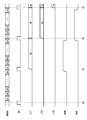
- FIG. 10 shows each signal waveform of the drive circuit 220 according to the present embodiment in S112.
- the control unit 140 outputs the precharge signal HVpchg in parallel to the n drive circuits 220.
- the second level shifter 290 of the drive circuit 220 outputs the drive voltage Vout at the H level to the corresponding electron beam generation source 212.
- control unit 140 supplies a plurality of enable signals Ena0 to Ena3 having a plurality of different rising periods to each drive circuit 220.
- control unit 140 supplies a plurality of enable signals Ena0 to Ena3 that rise at different timings and fall simultaneously to the drive circuit 220.
- the control unit 140 has a plurality of enable signals Ena0 that have a rising period of Ena1 of 90%, a rising period of Ena2 of 80%, and a rising period of Ena3 of 70%. ... Ena3 is supplied to the drive circuit 220.
- the drive circuit 220 supplies any one of the plurality of enable signals Ena0 to Ena3 to the first level shifter 280 according to the stored values of the registers LT1 and LT2.
- the first level shifter 280 supplies the second level shifter 290 with an enable signal Ena-i corresponding to one of the supplied enable signals Ena0 to Ena3.
- the second level shifter 290 switches the switches Tr1 and Tr4 from off to on in response to the rise of the enable signals Ena0 to Ena3. As a result, the second level shifter 290 causes the drive voltage Vout output to the electron beam generation source 212 to fall.
- the electron beam generation source 212 outputs an electron beam corresponding to the fall of the drive voltage Vout.
- the second level shifter 290 switches the switch Tr1 from on to off in response to the fall of the enable signals Ena0 to Ena3.
- the second level shifter 290 switches the switch Tr4 from on to off in response to the input of the precharge signal HVpchg from the control unit 140 again.
- the second level shifter 290 raises the drive voltage Vout.
- the electron beam generation source 212 stops outputting the electron beam.
- the second level shifter 290 receives the disable signal Dis from the control unit 140 via the first level shifter 280 and turns off the switches Tr2 and Tr3 of the second level shifter 290 in response to the rise of the disable signal Dis. Switch on. Accordingly, the second level shifter 290 prevents the drive voltage Vout from falling due to the input of the enable signals Ena0 to Ena3.
- FIG. 11 shows a modification of the drive circuit 220 of the electron beam irradiation apparatus 1000 according to the present embodiment.
- the same reference numerals are given to the substantially same operations as those of the drive circuit 220 according to the present embodiment shown in FIG.
- the drive circuit 220 may further include an AND circuit 256, an AND circuit 400, a third level shifter 402, a switch 404, a switch 406, and a switch 408.
- the drive device 219 may include an inspection control unit 410.
- the AND circuit 256 inputs the register specifying signal Md1, the register specifying signal Md0, and the write signal Wr, and outputs a logical product of these to the AND circuit 400. That is, when the register designation signal Md1 and the register designation signal Md0 from the control unit 140 are in the H level and the rising edge of the write signal Wr is input from the control unit 140, the AND circuit 256 sets the H level to the third level shifter 402. Output.
- the AND circuit 400 inputs the output from the shift register SR and the output from the AND circuit 256, and outputs a logical product of these to the third level shifter 402.
- the third level shifter 402 may be the same as the first level shifter 280.
- the third level shifter 402 receives the output from the AND circuit 400, converts the output voltage level, and outputs it to the switch 408.
- the third level shifter 402 outputs a 5V signal to the switch 408 in response to a signal having an H level of 1.8V being input from the AND circuit 400.
- the switch 404 may be a semiconductor switch, for example, a PMOS transistor in this modification.
- the switch 404 has a gate connected to the switch 412, a drain connected to the switches 406 and 408, and a source connected to the power supply voltage VH.
- the switch 406 may be a semiconductor switch, for example, a PMOS transistor in this modification.
- the switch 406 has a gate connected to the switch 404 and the switch 408, a drain connected to the inspection voltage HVout, and a source connected to the drive voltage Vout from the second level shifter.
- the switch 408 may be a semiconductor switch, for example, an NMOS transistor in this modification.
- the switch 408 has a gate connected to the output of the third level shifter 402, a drain connected to the switches 404 and 406, and a source connected to the reference potential VL.
- the inspection control unit 410 includes a switch 412 and a switch 414, and controls the output of the inspection voltage HVout by inputting the power supply voltage VH and the reference potential VL.
- the switch 412 may be a semiconductor switch, for example, a PMOS transistor in this modification.
- the drain and the gate of the switch 404 are connected to the gate, the gate and the switch 414 are connected to the drain, and the power supply voltage VH is connected to the source.
- the switch 414 may be a semiconductor switch, for example, an NMOS transistor in this modification.
- a ground potential via a load resistor and a reference potential via a load resistor are input to the gate, the switches 412 and 404 are connected to the drain, and the reference potential VL is connected to the source.
- the drive circuit 220 of this modification example receives the H-level register designation signal Md1, the register designation signal Md0, and the write signal Wr from the control unit 140 at the time of inspection, and outputs the output of the shift register Sr in response to the third signal. It outputs to the inspection voltage HVout through the level shifter and the switch 408 and the like. For example, the electron beam irradiation apparatus 1000 outputs the inspection voltage HVout to the inspection terminal 354.
- test voltage HVout of the plurality of drive circuits 220 is commonly connected, and after the control unit 140 resets the drive circuit 220 with the reset signal Rst, both the register designation signals Md0 and Md1 are set to 1, and 1 is set to the data signal SRdin.
- the clock signal SRckin By outputting and raising the clock signal SRckin, the level of the drive voltage Vout of the first drive circuit 220a is output to the commonly connected test voltage HVout.
- the control unit 140 when the control unit 140 outputs 0 to the data signal SRdin and raises the clock signal SRckin, the data signal SRdin having a value of 1 is sequentially input to the drive circuit 220 that is connected in cascade later, followed by The drive voltages Vout of the plurality of drive circuits 220 are sequentially output to the commonly connected inspection voltage HVout.
- the drive circuit 220 receives a plurality of enable signals Ena0 to 3 from the control unit 140. Instead, the individual drive circuits 220 include the enable signals Ena0 to Ena in the drive circuit 220. An exposure time pulse generation circuit for generating 3 may be included.
- the surface electron beam source 200 has an exposure time pulse generation circuit in the vicinity of the driving device 219, and the exposure time pulse generation circuit drives a plurality of enable signals Ena0 to 3 at a predetermined timing. It may be supplied to the circuit 220.
- the drive circuit 220 Operation can be checked. Therefore, according to the electron beam irradiation apparatus 1000 of this modification, the operation of the drive circuit 220 can be inspected without inspecting the electron beam output from the electron beam generation source 212.
Landscapes
- Chemical & Material Sciences (AREA)
- Analytical Chemistry (AREA)
- Electron Beam Exposure (AREA)
- Exposure And Positioning Against Photoresist Photosensitive Materials (AREA)
- Electron Sources, Ion Sources (AREA)
Abstract
電子ビーム照射装置のスループットを向上させる並列度を高め、露光の精度を高めた電子ビーム発生装置を提供すること。 第1の態様においては、複数の電子ビームによる描画パターンを対象物に照射する電子ビーム照射装置であって、複数の電子ビームを出力する複数の電子ビーム発生源が配列された面電子ビーム源と、複数の電子ビーム発生源のそれぞれの電子ビーム出力時間を調整する制御部とを備える電子ビーム照射装置を提供する。
Description
本発明は、電子ビーム照射装置に関する。
従来、微細パターンが設けられる半導体集積回路は、電子ビーム照射装置を用い、パターンデータに応じて少数の電子ビームを半導体基板に直接描画して当該微細パターンを形成していた(例えば、特許文献1および2参照)。
特許文献1 特開2007-329220号公報
特許文献2 特開平9-245708号公報
非特許文献1 P.N.Minh, L.T.T.Tuyen, T.Ono, H.Mimura, K.Yokoo and M.Esashi : Carbon nanotube on a Si tip for electron field emitter, Jpn. J. Appl. Phys., 41 Part2, 12A (2002), L1409-L1411
非特許文献2 P.N.Minh, L.T.T.Tuyen, T.Ono, H.Miyashita, Y.Suzuki, H.Mimura and M.Esashi : Selective growth of carbon nanotubes on Si microfabricated tips and application for electron field emitters, J. Vac. Sci. Technol. B 21, 4, (2003), 1705-1709
非特許文献3 P.N.Minh, T.Ono, N.Sato, H.Mimura and M.Esashi : Microelectron field emitter array with focus lenses for multielectron beam lithography based on silicon on insulator wafer, J.Vac.Sci.Technol., B22, 3 (2004) 1273-1276
非特許文献4 J.H.Bae, P.N.Minh, T.Ono and M.Esashi : Schottky emitter using boron-doped diamond, J.Vac.Sci.Technol., B22, 3 (2004) 1349-1352
非特許文献5 C.-H.Tsai, T.Ono and M.Esashi : Fabrication of diamond Schottky emitter array by using electrophoresis pre-treatment and hot-filament chemical vapor deposition, diamond and related materials, 16 (2007) 1398-1402
しかしながら、描画するパターンの微細化と、半導体ウェハの大口径化が進むことにより、電子ビーム照射装置のスループットが低下していた。スループットを改善する目的で、電子ビーム発生装置を小型化する動向にあるが、実際に作製して動作させることは困難であり、また、スループットと露光の精度を両立させることも困難であった。
本発明の第1の態様においては、複数の電子ビームによる描画パターンを対象物に照射する電子ビーム照射装置であって、複数の電子ビームを出力する複数の電子ビーム発生源が配列された面電子ビーム源と、複数の電子ビーム発生源のそれぞれの電子ビーム出力時間を調整する制御部とを備える電子ビーム照射装置を提供する。
なお、上記の発明の概要は、本発明の必要な特徴の全てを列挙したものではない。また、これらの特徴群のサブコンビネーションもまた、発明となりうる。
以下、発明の実施の形態を通じて本発明を説明するが、以下の実施形態は請求の範囲にかかる発明を限定するものではない。また、実施形態の中で説明されている特徴の組み合わせの全てが発明の解決手段に必須であるとは限らない。
図1は、本実施形態に係る電子ビーム照射装置1000の構成例を対象物10と共に示す。電子ビーム照射装置1000は、複数の電子ビームによる描画パターンを対象物10に照射し、対象物10に微細パターンを描画する。
対象物10は、半導体基板であってよく、例えば、シリコン、シリコンカーバイド、ゲルマニウム、ガリウムヒ素、窒化ガリウム、ガリウム燐、またはインジウム燐等の半導体材料の結晶を加工して形成された板状の基板でよい。対象物10には、電子線レジストが塗布されていてよい。電子ビーム照射装置1000は、電子ビーム照射部100と、ステージ部110と、記憶部120と、測定部130と、制御部140と、通信部150と、計算機部160とを備える。
電子ビーム照射部100は、複数の電子ビームを照射する電子カラムである。電子ビーム照射部100は、対象物10の表面に複数の電子ビームを照射して予め定められた描画パターンを描画する。電子ビーム照射部100の詳細は後に説明する。
ステージ部110は、電子ビームを照射する対象物10を載置する。ステージ部110は、載置した対象物10を水平方向に移動させ、電子ビーム照射部100によって対象物10の一方の面に、予め定められた微細パターンを予め定められた位置に描画させる。
ステージ部110は、例えば、ステージの水平平面を移動するXYステージを有する。また、ステージ部110は、予め定められた回転軸を中心として回転移動するθステージを有してよい。また、ステージ部110は、ステージの水平位置を調整するチルトステージを更に有してよい。また、ステージ部110は、対象物10を垂直方向に移動させ、対象物10および電子ビーム照射部100の間の距離を調節するZステージを更に有してよい。
記憶部120は、電子ビーム照射部100が描画する描画パターンデータを記憶する。ここで、描画パターンデータは、対象物10の一方の面上の位置データ、および電子ビームを照射するか否かの照射データ等の情報を含んでよい。記憶部120は、予め定められた描画パターンデータを予め記憶してよい。
測定部130は、電子ビーム照射部100の複数の電子ビームのそれぞれの強度を測定する。例えば、測定部130は、電子ビーム照射部100に電子ビームを個別に出力させて、出力させた電子ビームの強度を測定する。測定部130は、電子ビームの強度の測定結果を制御部140に供給する。
制御部140は、電子ビーム照射部100、ステージ部110、記憶部120、測定部130、及び通信部150にそれぞれ接続され、記憶部120に記憶された描画パターンデータに応じて、電子ビーム照射部100の電子ビーム照射及びステージ部110の動作を制御する。
例えば、制御部140は、記憶部120に記憶された複数の電子ビームの照射データを電子ビーム照射部100に送信することにより、電子ビーム照射部100の電子ビーム照射を制御する。また、制御部140は、記憶部120に記憶された描画パターンデータに応じて、ステージ部110を移動させる制御信号をステージ部110に送信することにより、ステージ部110の動作を制御する。また、制御部140は、通信部150を介して受け取った指示信号に応じて、電子ビーム照射部100および/またはステージ部110に制御信号を送信してよい。
また、制御部140は、測定部130の測定結果に基づいて、電子ビーム照射部100が出力する複数の電子ビームの出力時間を調整する。例えば、制御部140は、複数の電子ビームの強度の測定結果に基づいて各電子ビームの出力時間を決定し、当該出力時間を含む設定値を電子ビーム照射部100に供給する。
通信部150は、制御部140と計算機部160とを接続する。通信部150は、汎用または専用のインターフェイスを有して、制御部140と計算機部160とを接続して通信させてよい。通信部150は、Ethernet(登録商標)、USB、Serial RapidIO等の汎用の高速シリアルインターフェースまたはパラレルインターフェースを用いてよい。また、通信部150は、無線で制御部140と計算機部160とを接続してよい。
計算機部160は、制御部140に電子ビーム照射部100および/またはステージ部110を動作させる指示信号を送信する。計算機部160は、電子ビーム照射装置1000を動作させる動作プログラムを実行して、当該動作プログラムに応じて指示信号を送信してよい。また、計算機部160は、ユーザの指示を入力させる入力デバイスを有し、ユーザの指示に応じて指示信号を送信してよい。計算機部160は、パーソナルコンピュータまたはサーバマシンでよい。
図2は、本実施形態に係る電子ビーム照射部100の構成例を対象物10と共に示す。図2は、電子ビーム照射部100の縦断面の構成例を示す。電子ビーム照射部100は、面電子ビーム源200と、加速電極230と、電子レンズ240とを備える。
面電子ビーム源200は、複数の電子ビーム発生源212が配列され、制御部140から供給される電子ビームの出力時間の設定値に応じた期間、当該複数の電子ビーム発生源212から複数の電子ビームを出力する。面電子ビーム源200は、電子ビーム発生デバイス210と、駆動デバイス219とを有する。
電子ビーム発生デバイス210は、駆動デバイス219と張り合わされ、駆動デバイス219の反対側に、複数の電子ビームを出力する複数の電子ビーム発生源212を有する。電子ビーム発生デバイス210の電子ビームには、一定の電圧が印加され、一例として、略-5kVが印加される。電子ビーム発生デバイス210の詳細は後に説明する。
駆動デバイス219は、複数の電子ビーム発生源212を含む電子ビーム発生デバイス210の電子ビーム発生源212と反対側に貼り合わされて、複数の電子ビーム発生源212から電子ビームを出力させる。駆動デバイス219は、制御部140から照射データを受け取り、照射データに応じて、複数の電子ビーム発生源212に電子ビームを出力させる。
駆動デバイス219は、シリコン等の半導体基板で形成されてよい。駆動デバイス219は、面電子ビーム源200が駆動して温度が上昇しても電子ビーム発生デバイス210または駆動デバイス219に撓みまたは剥がれ等が生じない程度に、電子ビーム発生デバイス210の熱膨張係数とほぼ同じか、同程度の熱膨張係数を有する材料で形成されてよい。
加速電極230は、面電子ビーム源200の電子ビームを出力する側に備わり、面電子ビーム源200の電子ビームを出力させる電極よりも高い電圧が印加され、当該電子ビームを加速する。加速電極230は、複数の電子ビーム発生源212にそれぞれ対応する複数の貫通孔が形成され、複数の電子ビームをそれぞれ通過させる。加速電極230は、複数の貫通孔をマトリクス状に配列してよい。加速電極230は、一定の電圧が印加され、一例として、対象物10と共に略0Vが印加される。
電子レンズ240は、面電子ビーム源200から出力される複数の電子ビームによる描画パターンを予め定められた倍率にして対象物である対象物10に照射する。例えば、電子レンズ240は、複数の電子ビームが描画する描画パターンを1/100以下に縮小する。電子レンズ240は、コイル部242と、レンズ部244と、収束部246とを有する。
コイル部242は、複数の電子ビームのXY方向の偏向を制御する。即ち、コイル部242は、対象物10の電子ビームが照射される表面における当該電子ビームのビーム形状を制御する。コイル部242は、電子ビーム照射部100のX軸またはY軸と、対象物10の表面上のX軸またはY軸との対応を補正するローテーションコイルでよい。また、コイル部242は、対象物10の表面上のビーム径のXおよびY方向の振幅を補正してもよい。
レンズ部244は、対象物10の表面上に複数の電子ビームを結像させる。レンズ部244は、テレセントリックレンズ系を構成してよく、面電子ビーム源200の対物レンズとして機能する。
収束部246は、加速電界および/または減速電界を複数の電子ビームに印加する。収束部246は、複数の電子ビームの太さおよび束を絞って収束させて、予め定められたエネルギーの電子ビームを対象物である対象物10に照射する。
以上の本実施形態に係る電子ビーム照射部100は、面電子ビーム源等の複数の電子ビームを発生させる面電子ビーム源200を有し、1つの電子カラムから複数の電子ビームを試料に照射してスループットを向上させる。従来、このような複数の電子ビームを発生させる電子ビーム源を製造することは困難であったが、本実施形態に係る面電子ビーム源200は、半導体製造プロセス等の製造工程により、簡便に製造することができる。
図3は、本実施形態に係る面電子ビーム源200の構成例を示す。面電子ビーム源200は、複数の電子ビーム発生源212のそれぞれから放出される電子を加速して集束させ、複数の電子ビームとして出力する。面電子ビーム源200は、図2で説明したように、電子ビーム発生デバイス210と、駆動デバイス219とを有する。
また、面電子ビーム源200は、各部に電源電圧及び制御部140からの信号電圧等を供給する電圧供給部202を有してよい。また、面電子ビーム源200は、第1電極部310が障壁部330を介して接続される。
電圧供給部202は、定電圧発生回路および/または定電流発生回路と、複数の電極部204とを含み、それぞれの電極部204に接続される接続先にそれぞれ電源電圧等を供給する。電圧供給部202は、駆動デバイス219の電子ビーム発生デバイス210側とは反対側の面に設けられる。複数の電極部204は、ワイヤボンディング等で複数の接続先にそれぞれ接続されてよい。
ここで、本実施例で説明する電極部204等の電極は、ニッケル、金、クロム、チタン、アルミニウム、タングステン、パラジウム、ロジウム、白金、銅、ルテニウム、インジウム、イリジウム、オスミウム、および/またはモリブデンを含んでよい。また、当該電極は、これらの材料を含む2以上の材料の合金であってよい。
電子ビーム発生デバイス210は、シリコン等の半導体結晶から構成される基板211を有する。基板211には複数の凹部214と、アイソレーション部340と、第3電極部350とが設けられる。複数の凹部214は、それぞれが凹面を有し、それぞれに複数の電子ビーム発生源212a及び212bが形成される。また、複数の凹部214のそれぞれは、球面状または放物面状に形成されてよい。
複数の凹部214のそれぞれは、一例として、等方性エッチングにより形成され、電子ビームを発生させる電子ビーム発生源212a及び212bが形成される。例えば、複数の凹部214は、ウェットエッチングにより形成される。電子ビーム発生源212は、ポリシリコン層216と、第1絶縁膜215と、第2絶縁膜218と、電子放出部300と、第1電極部310と、第2電極部320と、障壁部330とを含む。
ポリシリコン層216は、基板211の複数の凹部214が形成された面に形成される。ポリシリコン層216のうち、凹部214に形成された少なくとも一部は、陽極活性され、ナノ結晶化された電子放出部300となる。
第1絶縁膜215および第2絶縁膜218は、基板211のポリシリコン層216が形成された面に形成される。第1絶縁膜215および第2絶縁膜218は、隣り合う電子ビーム発生源212のポリシリコン層216を電気的に絶縁して、当該ポリシリコン層216を介してリーク電流が発生することを防止する。第1絶縁膜215は、一例として、熱酸化によって形成されるSiO2膜等であり、また、第2絶縁膜218は、CVD法等によって成膜されるSiN膜である。
電子放出部300は、複数の凹部214のそれぞれに設けられ、電子を放出する。複数の凹部、即ち複数の電子放出部300は、基板211の一方の面にマトリクス状に配列され、駆動デバイス219からの駆動電圧に応じて電子をそれぞれ放出する。また、複数の電子放出部300のそれぞれは、ナノ結晶を有する。例えば、電子放出部300は、ナノ結晶シリコンで形成される。ナノ結晶シリコンは、電子トンネル障壁として機能する表面酸化膜を形成し、当該ナノ結晶シリコンが複数並ぶことにより、電子トンネル障壁を接続した列が形成される。
このような電子トンネル障壁の列は、当該障壁に電圧を印加することで、当該障壁を通過させる電子を、例えば数個の単位といった極微量な単位で制御することができる。したがって、電子放出部300は、ナノ結晶を有することで、電子の放出量を精密に、かつ、再現性よく制御することができる。
また、電子放出部300は、このようなナノ結晶シリコンが複数並ぶナノワイヤで形成される場合、電子を出力する面に対して当該ナノワイヤが垂直に形成されずに、結晶方位に依存して出力面の法線に対して傾くことがある。この場合、電子放出部300は、出力面の法線方向とは異なる方向に電子を出力させることがある。この場合、電子放出部300は、出力面の法線に対して異なる方向のトンネル確率の分布と、当該方向にナノワイヤが電子を放出する分布との掛け算で、電子放出量が定まる。
電子放出部300は、凹面形状の凹部214を有することで、当該凹面形状を平坦な形状にした場合の電子放出量に比べてより多くの電子を有効な電子ビームとして外部に出力させることができる。例えば、電子放出部300は、電子を放出する分布がより高い方向および/またはトンネル確率の分布がより高い方向を、電子ビームを出力する方向に向けて形成することで、平坦な形状にした場合の電子放出量に比べてより多くの電子を電子ビームとして出力させることができる。一例として、凹部214の形状は、複数の電子放出部300の電子を放出する方向と、当該方向の電子のトンネル確率との乗算がより大きくなる方向を、対応する第1電極部310の開口部に向ける。
また、複数の電子放出部300のそれぞれは、ナノ結晶に代えて、放出する電子をトンネリングさせる絶縁膜を有してよい。このような絶縁膜は、放出する電子の量をトンネルする確率によって調整することができるので、当該絶縁膜の材質、膜厚および絶縁膜に印加する電圧によって、電子の放出量を制御することができる。
第1電極部310は、複数の電子放出部300のそれぞれに対応して設けられ、対応する電子放出部300が放出した電子を加速して電子放出部300に設けられた凹部214から電子ビームとして出力する。複数の第1電極部310のそれぞれは、開口部312を有し、基板211の複数の凹部214が設けられる一方の面に板状に形成され、対応する凹部214との電位差によって開口部312から電子ビームを集束させて出力させる。開口部312は、第1電極部310および/または電子放出部300の中心近辺に形成される。開口部312は、円形の貫通孔でよい。
図中において、第1電極部310aは、電子放出部300aに対応して設けられ、電子放出部300aが放出する電子を加速して開口部312aから電子ビームとして出力させる例を示す。同様に、第1電極部310bは、電子放出部300bに対応して設けられ、電子放出部300bが放出する電子を加速する。ここで、複数の第1電極部310(図中の例では第1電極部310aおよび第1電極部310b)は、電気的に接続され、予め定められた定電圧が印加される。
第1電極部310は、基板211の外部に備わる電極等と電気的に接続され、制御部140からの駆動電圧等が印加される接続部を有してよい。当該接続部は、第1電極部の一部にメッキ等で導電性物質が更に形成された電極部でよい。接続部は、ワイヤボンディング等によって外部の電極と接続されてよい。
第2電極部320は、複数の凹部214のそれぞれに設けられ、当該凹部214を覆う導電性物質で形成される。第2電極部320は、電子放出部300から放出された電子を、第1電極部310との電位差によって開口部312から電子ビームとして出力させる。ここで、第2電極部320は、電子放出部300から放出される電子を通過させる程度に薄く形成される。複数の凹部214に設けられる複数の第2電極部320は、電気的に接続され、予め定められた定電圧が印加される。
ここで、第1電極部310および第2電極部320は、これら電極間の電位差が数十から数百Vとなる駆動電圧がそれぞれ印加されてよい。好ましくは、第1電極部310および第2電極部320は、制御部140から電位差が百数十Vとなる駆動電圧がそれぞれ印加される。一例として、第1電極部310および第2電極部320は、電位差が150Vとなる駆動電圧がそれぞれ印加される。第2電極部320は、接続部322を含む。
接続部322は、第2電極部320のうち厚さがより厚く形成される電極部であって、基板211の外部に備わる電極等と電気的に接続され、駆動電圧が印加される。接続部322は、第2電極部の一部にメッキ等で導電性物質が更に形成された電極部でよい。接続部322は、ワイヤボンディング等によって外部の電極と接続されてよい。
障壁部330は、複数の第1電極部310および基板211の間において複数の凹部214に対応する位置に設けられ、絶縁材料で形成される。障壁部330は、基板211と第1電極部310との間を予め定められた距離を離間させ、第1電極部310を支持しつつ、第1電極部310と第2電極部320とを電気的に絶縁する。障壁部330は、樹脂等で形成されてよく、これに代えて、CVD法等によって成膜される酸化シリコン膜でよい。
以上の電子ビーム発生源212は、電子放出部300が放出する電子に、第1電極部310と第2電極部320にそれぞれ印加される駆動電圧によって生じる電界を印加することによって開口部312から電子ビームを発生させる。ここで、電子ビーム発生源212は、凹部214が凹面状、球面状、または放物面状に形成されることで、電子放出部300の電子を放出する面もまた凹面状、球面状、または放物面状に形成される。
これによって、電子ビーム発生源212は、電子放出部300が電子を放出する方向を開口部312の方向に合わせて、当該開口部312に集束させやすくすることができる。即ち、電子ビーム発生源212は、開口部312に集束させる電子の数を増加させることができ、発生する電子ビームの密度を高めることができる。
電子ビーム発生源212は、発生させた電子ビームを後段の電子レンズ240によって対象物10に照射させる。ここで、電子レンズ240は、光学レンズ等と同様に電子ビームの結像にボケやゆがみ等を生じさせる収差を有する場合がある。例えば、電子レンズ240は、結像させる電子ビームに対して、ビームの中央近傍を走行する電子に比べてビームの外側近傍を走行する電子の焦点位置を短くさせる場合がある。
そこで、電子ビーム発生源212は、電子放出部300の電子を放出する面を凹面状、球面状、または放物面状に形成させて電子ビームの密度を高めつつ、当該収差を補正してよい。ここで、電子ビーム発生源212が凹部214を平坦にした場合、電子放出部300の電子の放出面の法線方向が開口部312近傍にある領域から出力される電子は、電子ビームの中央に集束されやすい。
そこで電子放出部300は、電子の放出面を開口部312に向けつつ、当該領域である放出面の中央近傍の領域と開口部312との間の距離よりも、放出面の縁側近傍の領域と開口部312との間の距離を、より短くする面を形成する。即ち、電子ビームの外側に集束されやすい電子がより速く開口部312に到達するように放出面を形成することで、当該電子の焦点距離を長くさせる。これは、凹部214が、電子放出部300の放出面の中心点により近い部分から放出される電子の層流を、当該中心点により近い位置に集中させて負の収差を発生させることに相当する。
これによって、電子ビーム発生源212は、発生させる電子ビームの中央近傍(例えば、図3におけるA-A'、B-B'で示した凹部214の略中央を通る垂線近傍)を走行する電子に比べて、電子ビームの外側近傍を走行する電子の焦点距離を長くすることができる。例えば、電子ビーム発生源212は、電子ビームの光軸の中心から離れるに応じて電子ビームの焦点距離を長くして、電子ビームの照射方向に対する垂直方向の断面において、同心円状に焦点距離の分布を持たせる。このように、電子ビーム発生源212は、電子レンズ240の収差に対応させた放出面を形成することで、電子レンズ240の収差を補正することができる。
また、電子放出部300の放出面の縁側近傍の領域は、中央近傍の領域に比べて電子ビーム発生源212の外部に近いので、外部電界の影響を受けやすい。即ち、放出面の縁側近傍の領域から出力される電子は、放出面の法線から傾いた方向に出力されやすく焦点距離が長くなりやすい。このように、電子ビーム発生源212は、外部電界に依存して出力させる電子ビームに焦点距離の分布を形成させるので、このような分布に応じて、電子放出部300の放出面の形状を調整して対象物10に結像する電子ビームの収差を補正してよい。
ここで、第2電極部320は、凹部214を覆う電極を形成し、当該凹部214を同電位に保つ。これによって、第2電極部320は、電子放出部300から安定な速度分布の電子を放出させて開口部312近傍に集束させつつ、上記の外部電界の影響を低減させることができる。
アイソレーション部340は、絶縁物質が充填されて形成される。アイソレーション部340は、複数の電子ビーム発生源212のそれぞれの周囲を囲むように形成され、電子ビーム発生源212間を電気的に分離する。アイソレーション部340は、一例として、基板211の複数の凹部214が形成される面とは反対側の面において、複数の電子放出部300に対応する複数のリング状または格子状に形成された溝に樹脂等の絶縁材料を充填させて形成される。
第3電極部350は、基板211の複数の凹部214が形成される上面とは反対側の下面に、複数の電子放出部300のそれぞれに対応して形成される。第3電極部350は、複数の電子放出部300から電子をそれぞれ放出させる駆動電圧がそれぞれ印加される。第3電極部350は、基板211の下面に形成される導電膜352を有してよい。第3電極部350は、駆動デバイス219と電気的に接続される。
駆動デバイス219は、複数の電子ビーム発生源212a及び212bのそれぞれに対応する、複数の駆動回路220a及び220bを有する。駆動回路220a及び212bは、複数の電子ビーム発生源212のそれぞれを駆動する駆動電圧を供給する。
具体的には、駆動回路220は、複数の電子放出部300から電子を放出させる駆動電圧を、複数の電子放出部300のそれぞれに対して個別に供給する。駆動回路220a等は、半導体基板に形成され、当該半導体基板の一方の面を基板211と張り合わされてよい。
ここで駆動回路220は、基板211に形成される第3電極部350に対応する複数の電極部222を有し、当該電極部222が対応する第3電極部350と電気的に接続されつつ基板211と張り合わされ、当該電極部222を介して駆動電圧を供給する。電極部222は、例えば、100μmピッチ程度で基板211に形成される第3電極部350に対応させるべく、当該第3電極部350と同程度のピッチで形成される。
駆動回路220は、外部に備わる電極等と電気的に接続され、駆動電圧および電源電圧等が印加される複数の接続部224を有してよい。当該接続部224は、ワイヤボンディング等によって外部の電極と接続されてよい。
複数の駆動回路220の少なくとも1つは、電圧供給部202を介して外部に露出されて、駆動電圧を出力する検査用端子354を有してよい。検査用端子354は、検査時において、駆動回路220から対応する電子ビーム発生源212に供給する駆動信号を駆動デバイス219における電子ビーム発生デバイス210とは反対側の面へと出力する。
駆動回路220は、複数の電子放出部300のそれぞれの配置に応じて、異なるオフセットバイアスを更に印加してよい。複数の電子放出部300は、それぞれ個別に駆動電圧を印加されて電子をそれぞれ放出し、対応する複数の電子ビーム発生源212は、複数の電子ビームを発生させる。複数の電子ビーム発生源212a等は、発生させた複数の電子ビームを後段の電子レンズ240によって結像させて、対象物10に描画パターンを照射させる。
ここで、電子レンズ240等の光学系は、レンズの中央近傍を通る電子ビームと、レンズの外縁近傍を通る電子ビームとで僅かに焦点位置に差を与え、複数の電子ビームによる描画像にボケやゆがみ等を生じさせる場合がある。例えば、電子レンズ240は、レンズの外縁近傍を通る電子ビームに対して、レンズの中央近傍を通る電子ビームに比べて焦点位置を短くさせる場合がある。
そこで、駆動回路220は、電子レンズ240の中央近傍を通る電子ビームを発生させる電子ビーム発生源212に比べて、電子レンズ240の外縁近傍を通る電子ビームを発生させる電子ビーム発生源212に対して、高いオフセット電圧を供給する。これによって、駆動回路220は、電子レンズ240の外縁近傍を通る電子ビームの出力速度を増加させて焦点距離を長くして発生させ、電子レンズ240によって短くなる焦点位置と相殺させて補正することができる。
ここで、複数の電子放出部300は、それぞれの配置に応じて複数のブロックに分配され、駆動回路220は、当該ブロック毎にオフセットバイアスを印加してよい。例えば、複数の電子放出部300のうち、基板211の一方の面上において中央近辺に配置され、電子レンズ240の中央近傍を通る電子ビームとなる電子を放出する複数の電子放出部300は、同一のブロックに分配される。また、その他の電子放出部300は、中央のブロックを中心に、略同心円状に2以上のブロックに分配されてよい。
このように、複数の電子放出部300は、電子レンズ240の中央近傍を通る電子ビームを出力させる電子放出部300を中心ブロックとして、電子レンズ240の外縁方向に同心円状に2以上に分割された環状領域に対応する電子放出部300を、他のブロックとして分配される。駆動回路220は、当該ブロック毎に異なるオフセットバイアスを印加することで、電子レンズ240の中央近傍を通る電子ビームを中心に、同心円状に分割された領域毎に電子ビームの焦点位置を調節することができ、効率的に描画パターンの結像を補正することができる。
駆動回路220は、第1電極部310および第2電極部320に、数kV~数十kVの負電圧を印加する。一例として、駆動回路220は、同心円の中央に分配された電子放出部300に対応する第2電極部320に-5kVを、対応する第1電極部310に-5kV+150Vを印加する。
この場合、電子ビーム発生源212は、150Vの電位差によって生じる電界を電子放出部300から放出する電子に印加して電子ビームを発生させ、発生した電子ビームを加速電極230との略5kVの電位差で加速させる。また、駆動回路220は、中央のブロックから外縁に向けてnブロック異なる毎に、対応する第2電極部に-5kV+nVを、対応する第1電極部に-5kV+150V+nVを印加する。このように、駆動回路220は、ブロックが異なる毎に駆動電圧を1V程度変化させて、電子ビームの加速電界をブロック毎に微調整してよい。
以上の本実施例に係る面電子ビーム源200は、複数の電子ビーム発生源212を有し、当該複数の電子ビーム発生源212をそれぞれ個別に駆動して複数の電子ビームを出力させることができる。これによって、面電子ビーム源200を備える電子ビーム照射部100は、複数の電子ビームによって予め定められた描画パターンを対象物に照射することができる。
ここで、電子ビーム発生源212は、半導体基板に等方性エッチング等の簡便な方法で形成された複数の凹部214にそれぞれ形成される。したがって、複数の電子ビーム発生源212は、半導体製造プロセス等によって基板211に形成することができる。即ち例えば、電子ビーム発生源212は、基板211の1cm×1cmの面積に、100×100個のマトリクス状に配列されて形成される。このように、電子ビーム発生源212は、100μm程度のピッチのマトリクス状に形成することで、電子レンズ240によって1μm以下程度のピッチの描画パターンを対象物に照射することができる。
また、面電子ビーム源200に備わる電子ビーム発生源212は、複数の凹部214と、複数の凹部214に対応する位置に別プロセスで形成させた障壁部330とを有する。これによって、面電子ビーム源200は、凹面状、球面状、または放物面状といった予め定められた形状の底部を有する円柱状の穴等を精密に形成すること無しに、複数の電子ビーム発生源212を簡便に形成することができる。このように、面電子ビーム源200は、小面積、かつ、高密度に形成させた複数の電子ビーム発生源212を備えることができる。したがって、電子ビーム照射部100は、装置の大きさを小型にしつつ、10000程度の電子ビームを照射することができる。
以上の本実施例において、面電子ビーム源200および電子ビーム照射部100は、電子ビーム照射装置1000に用いられる例を説明した。これに代えて、面電子ビーム源200および電子ビーム照射部100は、電子ビームを用いる装置に備わってよく、電子顕微鏡、電子線マイクロアナライザ、ブラウン管、送信管、撮像管、真空管、加工装置、加熱装置、または滅菌装置等に用いられてもよい。
図4は、制御部140及び複数の駆動回路220a~dを示す。複数の駆動回路220a~dは、制御部140に対して縦続接続され、制御部140からのデータを駆動回路220a、駆動回路220b、駆動回路220c、駆動回路220dの順に伝播していくことによりデータを伝送する。
制御部140は、直列に縦続接続される複数の駆動回路220a~dに対してシーケンシャルに照射データを出力して、複数の駆動回路a~dに照射データを書き込ませる。また、制御部140は、複数の駆動回路220a~dに対してシーケンシャルに電子ビーム出力時間の設定値を出力して、複数の駆動回路220a~dのそれぞれに対し当該設定値を設定する。
例えば、制御部140は、駆動回路220aのシフトレジスタSRに順次照射データを送信し、照射データをシフトレジスタ間でシフトさせていくことにより、複数の駆動回路220a~dのシフトレジスタSRに、複数の駆動回路220a~dに対応する電子ビーム発生源212a~d用の照射データを格納する。制御部140は、複数の駆動回路220a~dに対してシフトレジスタSRの値をレジスタLT0に格納する命令を送信することにより、複数の駆動回路220a~dのレジスタLT0に照射データを格納する。
制御部140は、同様の方法により、複数の駆動回路220a~dのレジスタLT1及びLT2に、各駆動回路220a~dに対応する電子ビーム発生源212の出力時間の設定値を格納する。これにより、駆動回路220a~dの各々は出力時間の設定値として2ビット(4段階)の値を格納する。なお、駆動回路220a~dの照射データ用のレジスタは2ビット以上でもよく、設定値のレジスタは3ビット以上又は1ビットであってもよい。
図5は、複数の駆動回路220のグループを示す(同心円状にブロック分割された電子源アレイの1/4部分のみ表示)。本実施形態において、複数の駆動回路220は、複数のグループに分割されてよく、駆動回路220がグループ毎に縦続接続されてもよい。図示するように、面電子ビーム源200の領域は、電子ビームの焦点距離ごとに複数の同心円に囲まれたブロックにより分割される。
さらに同心円に囲まれた1つのブロックは、複数のグループG1及びグループG2等により分割される。複数の駆動回路220は、グループごとに縦続接続されており、制御部140は、複数のグループのそれぞれに含まれる複数の駆動回路220に対して、矢印で示すようにシーケンシャルに照射データ等を出力して複数の駆動回路220に書き込ませる。
図6は、駆動回路220の構成を示す。駆動回路220は、制御部140から書き込まれた照射データ及び出力時間の設定値に基づいて、対応する電子ビーム発生源212に駆動電圧を供給する。駆動回路220は、シフトレジスタSR、レジスタLT0、レジスタLT1、レジスタLT2、バッファアンプ248、AND回路250、AND回路252、AND回路254、AND回路260、AND回路262、AND回路264、AND回路266、OR回路268、AND回路270、AND回路272、OR回路274、第1レベルシフタ280、及び、第2レベルシフタ290を有する。
駆動回路220は、制御部140からクロック信号SRckin及びデータ信号SRdinを入力し、クロック信号SRckin及びデータ信号SRdinを後続の駆動回路220に供給する。後続の駆動回路220は、前に接続された駆動回路220からクロック信号SRckin及びデータ信号SRdinを入力し、後続の駆動回路220に供給する。
駆動回路220は、制御部140から、予め定められた長さの立ち上がり期間を有する複数のイネーブル信号Ena0~3、レジスタ指定信号Md0、レジスタ指定信号Md1、ライト信号Wr、ディセーブル信号Dis、及び、リセット信号Rstを入力する。これらの信号は、制御部140に対して1対多で接続されてよく、これに代えて制御部140に対して縦続接続されてもよい。
バッファアンプ248は、制御部140又は前に接続される駆動回路220からクロック信号を入力し、当該クロック信号を増幅して後に接続される駆動回路220に供給する。
シフトレジスタSRは、データ入力Dに制御部140又は前に接続される駆動回路220のシフトレジスタが接続され、データ出力Qに後続の駆動回路220のシフトレジスタが接続され、リセット入力Rに制御部140が接続される。シフトレジスタSRは、データ入力Dに制御部140又は前に接続された駆動回路220からデータ信号SRdinを入力し、クロック信号SRckinで示されるタイミング(例えば、立ち上がりタイミング)で当該データ信号SRdinを取り込む。そして、シフトレジスタSRは、レジスタLT0、レジスタLT1、レジスタLT2、及び、後に接続される駆動回路220に対し、取り込んだデータ信号SRdinを出力する。また、シフトレジスタSRは、制御部140からリセット信号Rstを入力する。
AND回路250は、レジスタ指定信号Md0の反転値、レジスタ指定信号Md1の反転値、及び、ライト信号Wrを入力し、これらの論理積をレジスタLT0に出力する。AND回路252は、レジスタ指定信号Md0、レジスタ指定信号Md1の反転値、及び、ライト信号Wrを入力し、これらの論理積をレジスタLT1に出力する。AND回路254は、レジスタ指定信号Md0の反転値、レジスタ指定信号Md1、及び、ライト信号Wrを入力し、これらの論理積をレジスタLT2に出力する。
レジスタLT0は、データ入力DにシフトレジスタSRの出力Qが接続され、クロック入力EにAND回路250の出力が接続される。レジスタLT0は、AND回路250の出力をイネーブル信号として入力し、AND回路250からの出力が立ちあがった状態で、シフトレジスタSRの出力値を格納する。これにより、レジスタLT0は、制御部140がLレベルのレジスタ指定信号Md0を出力し、Lレベルのレジスタ指定信号Md1を出力した状態で、ライト信号Wrの立ち上がり時にシフトレジスタSRの出力を格納する。
また、レジスタLT0は、リセット入力Rに制御部140が接続されて制御部140からリセット信号Rstを入力する。レジスタLT0は、AND回路260、AND回路262、AND回路264及びAND回路266に格納した値を出力する。
レジスタLT1は、データ入力DにシフトレジスタSRの出力Qが接続され、クロック入力EにAND回路252の出力が接続される。レジスタLT1は、AND回路252からの出力が立ちあがった状態で、シフトレジスタSRの出力値を格納する。これにより、レジスタLT1は、制御部140がHレベルのレジスタ指定信号Md0を出力し、かつLレベルのレジスタ指定信号Md1を出力した状態で、ライト信号Wrの立ち上がり時にシフトレジスタSRの出力を格納する。
また、レジスタLT1は、リセット入力Rに制御部140が接続されて制御部140からリセット信号Rstを入力する。レジスタLT1は、AND回路260、AND回路262、AND回路264及びAND回路266に格納した値を出力する。
レジスタLT2は、データ入力DにシフトレジスタSRの出力Qが接続され、クロック入力EにAND回路254の出力が接続される。レジスタLT2は、AND回路254からの出力が立ちあがった状態で、シフトレジスタSRの出力値を格納する。これにより、レジスタLT2は、制御部140がLレベルのレジスタ指定信号Md0を出力しHレベルのレジスタ指定信号Md1を出力した状態で、ライト信号Wrの立ち上がり時にシフトレジスタSRの出力を格納する。
また、レジスタLT2は、リセット入力Rに制御部140が接続されて制御部140からリセット信号Rstを入力する。レジスタLT2は、AND回路260、AND回路262、AND回路264及びAND回路266に格納した値を出力する。
AND回路260は、レジスタLT1の出力の反転値、レジスタLT2の出力の反転値、及び、制御部140からのイネーブル信号Ena0を入力し、これらの論理積をOR回路268に出力する。すなわち、AND回路260は、レジスタLT1に格納された値が0、レジスタLT2に格納された値が0の場合、イネーブル信号Ena0の立ち上がり期間に対応してOR回路268にHレベル信号を出力する。
AND回路262は、レジスタLT1の出力、レジスタLT2の出力の反転値、及び、制御部140からのイネーブル信号Ena1を入力し、これらの論理積をOR回路268に出力する。すなわち、AND回路262は、レジスタLT1に格納された値が1、レジスタLT2に格納された値が0の場合、イネーブル信号Ena1の立ち上がり期間に対応してOR回路268にHレベル信号を出力する。
AND回路264は、レジスタLT1の出力の反転値、レジスタLT2の出力、及び、制御部140からのイネーブル信号Ena2を入力し、これらの論理積をOR回路268に出力する。すなわち、AND回路264は、レジスタLT1に格納された値が0、レジスタLT2に格納された値が1の場合、イネーブル信号Ena2の立ち上がり期間に対応してOR回路268にHレベル信号を出力する。
AND回路266は、レジスタLT1の出力、レジスタLT2の出力、及び、制御部140からのイネーブル信号Ena3を入力し、これらの論理積をOR回路268に出力する。すなわち、AND回路266は、レジスタLT1に格納された値が1、レジスタLT2に格納された値が1の場合、イネーブル信号Ena3の立ち上がり期間に対応してOR回路268にHレベル信号を出力する。
OR回路268は、AND回路260、AND回路262、AND回路264及びAND回路266からの出力を入力し、これらの入力の論理和をAND回路270に出力する。これにより、OR回路268は、イネーブル信号Ena0~3のいずれか1つの立ち上がり期間に対応してHレベル信号を出力する。
AND回路270は、レジスタLT0及びOR回路268の出力を入力し、これらの論理積をイネーブル信号Enaとして第1レベルシフタ280に出力する。すなわち、AND回路270は、LT0に1が格納される場合に、イネーブル信号Ena0~3のいずれか1つの立ち上がり期間に対応してHレベル信号を出力する。
AND回路272は、レジスタLT0の反転値及び制御部140からのディセーブル信号Disを入力し、これらの論理積をOR回路274に出力する。
OR回路274は、AND回路272及び制御部140からのリセット信号Rstを入力し、これらの論理和をディセーブル信号として第1レベルシフタ280に入力する。
第1レベルシフタ280は、AND回路270、OR回路274及び第2レベルシフタ290に接続され、AND回路270からイネーブル信号Enaを入力し、OR回路274からディセーブル信号Disを入力し、これらの入力信号の電圧レベルを変換したのち、対応するイネーブル信号Ena-i及びディセーブル信号Dis-iを第2レベルシフタ290に出力する。
例えば、第1レベルシフタ280は、Hレベルが1.8Vのイネーブル信号Enaを入力したことに応じて5Vのイネーブル信号Ena-iを出力し、Hレベルが1.8Vのディセーブル信号Disを入力したことに応じて5Vのディセーブル信号Dis-iを出力する。
第2レベルシフタ290は、第1レベルシフタ280及び電子ビーム発生源212に接続され、制御部140からプリチャージ信号HVpchgを入力し、第1レベルシフタ280からイネーブル信号Ena-iを入力し、プリチャージ信号HVpchgに応じてイネーブル信号Ena-iよりも高電圧の駆動電圧を電子ビーム発生源212に出力する。
例えば、第2レベルシフタ290は、20Vの電源電圧VH及び0Vの基準電圧VLを入力し、プリチャージ信号HVpchgからプリチャージ信号が入力されると電子ビーム発生源212にHレベルの駆動電圧を出力する。また、第2レベルシフタ290は、第1レベルシフタ280からのイネーブル信号Ena-iが入力されてから再びプリチャージ信号HVpchgが入力されるまでの間、電子ビーム発生源212にLレベルの駆動電圧を出力する。また、第2レベルシフタ290は、ディセーブル信号Dis-iが入力される期間、Lレベルの駆動電圧を電子ビーム発生源212に出力しない。
図7は、第2レベルシフタ290の構成を示す。第2レベルシフタ290は、電源電圧VH及び基準電圧VLを入力し、制御部140からプリチャージ信号HVpchgを入力し、第1レベルシフタ280からのイネーブル信号Ena-i及びディセーブル信号Dis-iを入力し、駆動電圧Voutを電子ビーム発生源212に供給する。第2レベルシフタ290は、スイッチTr1、スイッチTr2、スイッチTr3、スイッチTr4、スイッチTr5、及び、スイッチTr6を備える。
スイッチTr1は、半導体スイッチであってよく、例えば、本実施形態においてはNMOSトランジスタである。スイッチTr1は、ゲートが第1レベルシフタ280に接続されてイネーブル信号Ena-iを入力し、ドレインがスイッチTr3及び駆動電圧Voutに接続され、さらにドレインが抵抗を介してスイッチTr4及びスイッチTr6に接続され、ソースが基準電位VLに接続される。
スイッチTr2は、半導体スイッチであってよく、例えば、本実施形態においてはNMOSトランジスタである。スイッチTr2は、ゲートが第1レベルシフタ280に接続されてディセーブル信号Dis-iを入力し、ドレインがスイッチTr4に接続され、さらにドレインが抵抗を介してスイッチTr3及びスイッチTr5に接続され、ソースが基準電位VLに接続される。
スイッチTr3は、半導体スイッチであってよく、例えば、本実施形態においてはPMOSトランジスタである。スイッチTr3は、ゲートが抵抗を介してスイッチTr2及びスイッチTr4に接続され、ソースが電源電圧VHに接続され、ドレインがスイッチTr1、駆動電圧Voutに接続され、さらにドレインが抵抗を介してスイッチTr2及びTr4に接続される。
スイッチTr4は、半導体スイッチであってよく、例えば、本実施形態においてはPMOSトランジスタである。スイッチTr4は、ゲートがスイッチTr6に接続され、さらにゲートが抵抗を介したスイッチTr1及びスイッチTr3に接続され、ソースが電源電圧VHに接続され、ドレインがスイッチTr2に接続され、さらにドレインが抵抗を介してスイッチTr3及びスイッチTr5に接続される。
スイッチTr5は、半導体スイッチであってよく、例えば、本実施形態においてはPMOSトランジスタである。スイッチTr5は、ゲートがスイッチTr6に接続され、制御部140からプリチャージ信号HVpchgを入力し、ソースが電源電圧VHに接続され、ドレインがスイッチTr3に接続され、さらにドレインが抵抗を介してスイッチTr2及びスイッチTr4に接続される。
スイッチTr6は、半導体スイッチであってよく、例えば、本実施形態においてはPMOSトランジスタである。スイッチTr6は、ゲートがスイッチTr5に接続されてスイッチTr5とカレントミラー回路を形成する。また、スイッチTr6は、ゲートが制御部140に接続されて制御部140からのプリチャージ信号HVpchgを入力し、ソースが電源電圧VHに接続され、ドレインがスイッチTr4に接続され、さらにドレインが抵抗を介してスイッチTr1及びスイッチTr3に接続される。
プリチャージ信号HVpchgがHレベルの場合、スイッチTr5及びTr6がオフとなる。この状態でイネーブル信号Ena-iが入力されるとスイッチTr1がオンとなり、スイッチTr1のソース側がスイッチTr1を介して基準電位VLに接続されることによって、スイッチTr4のゲートがLレベルとなってスイッチTr4がオンとなる。この結果、スイッチTr3のゲートがスイッチTr4を介して電源電圧VHに接続され、スイッチTr3がオフとなる。この結果、第2レベルシフタ290は、駆動電圧Voutが基準電位VLに低下する。
このようにして、第2レベルシフタ290は、スイッチTr1~Tr4により、低電圧(例えば、5V)の制御部140からのイネーブル信号Ena-iの立ち上りに応じて高電圧(例えば、20V)の駆動電圧Voutを立下げる。電子ビーム発生源212は駆動電圧Voutの立下りを受けて電子ビームを出力する。第2レベルシフタ290は、制御部140からのディセーブル信号Dis-iにより駆動電圧Voutの出力をディセーブルする。
また、第2レベルシフタ290は、スイッチTr5及びTr6をオンとし、プリチャージ信号HVpchgの立ち下りに応じて駆動電圧Voutを立ち上げる。第2レベルシフタ290は、スイッチTr5及びスイッチTr6によりスイッチTr3及びスイッチTr4のオン・オフを制御することにより、電源電圧VHから基準電位VLに貫通電流が流れるのを防止する。
このように、図1~7に示した本実施形態の電子ビーム照射装置1000によると、複数の電子ビーム発生源212の駆動回路220のレジスタLT0~LT2に照射データ及び電子ビームの出力時間を格納する。従って、電子ビーム照射装置1000によれば、電子ビーム発生源212ごとに最適な電子ビームの出力時間を設定することができ、これにより、面電子ビーム源200は、電子ビーム発生源212ごとに電子放出強度(電流密度)にばらつきのない電子ビームを出力し、対象物10に均一なドーズ量の電子ビームを照射することができる。本実施形態の電子ビーム照射装置1000によれば、出力する電子ビームにばらつきがある面電子ビーム源200を対象物の露光に使用することができるので、電子ビーム照射装置の量産性及び製造コストを改善することができる。
図8は、本実施形態に係る電子ビーム照射方法の処理フローを示す。電子ビーム照射装置1000は、S102からS112までの処理を実行することにより、対象物10に予め定められた描画パターンを描画する。
まず、S102において、制御部140は、電子ビーム照射部100の複数の電子ビーム発生源212を順次駆動し、各々の電子ビーム発生源212に電子ビームを出力させる。ここで、制御部140は、複数の電子ビーム発生源212の各電子ビームに同一の出力時間で電子ビームを出力させてよい。
次に、S104において、測定部130は、各電子ビーム発生源212が出力した電子ビームの強度を測定する。例えば、測定部130は、電子線検出器により電子ビーム発生源212が出力する電子ビームの強度を例えば微小電流計により測定する。測定部130は、電子ビームの強度の測定結果を制御部140に供給する。
次に、S106において、制御部140は、測定部130の測定した電子ビーム発生源212の出力する電子ビームの強度に応じて、各電子ビーム発生源212の電子ビームの出力時間を設定する。
例えば、制御部140は、測定部130が測定した複数の電子ビームのそれぞれの強度に応じて、予め定められた電子ビーム出力時間に対して複数の電子ビームのそれぞれの電子ビーム出力時間を調整して、照射量のバラツキを低減する。具体的には、制御部140は、測定された出力強度が高い電子ビームに対して短い電子ビーム出力時間を設定し、出力強度が低い電子ビームに対して長い電子ビーム出力時間を設定してよい。一例として、制御部140は、各電子ビームに対して、測定された出力強度に反比例する電子ビーム出力時間を設定してよい。
また、例えば、制御部140は、一の電子ビームが対象物10に照射される照射位置に対して予め定められた範囲内に照射される描画パターンに基づいて、予め定められた電子ビーム出力時間に対して当該一の電子ビームを出力する電子ビーム出力時間を調整することにより、描画パターンの近接効果による各電子ビームの最適露光時間の違いを補償する。
一例として、制御部140は、対象物10に照射される照射位置が一の電子ビームに対して隣接する隣接電子ビームの描画パターンに基づいて、予め定められた電子ビーム出力時間に対して当該一の電子ビームを出力する電子ビーム出力時間を調整してよい。具体的には、制御部140は、予め定められた範囲において隣接して配置される複数の電子ビームの数が大きいほど、一の電子ビームの電子ビーム出力時間を低減してよい。
別の一例として、制御部140は、一の電子ビームが対象物10に照射される照射位置に対して予め定められた範囲内に照射される描画パターンと対象物10及び対象物10上のレジスト等の種類とに基づいて、予め定められた電子ビーム出力時間に対して当該一の電子ビームの電子ビーム出力時間を調整してよい。
制御部140は、調整された電子ビーム出力時間の設定値を、電子ビーム照射部100の複数の駆動回路220に供給して、駆動回路220のレジスタLT1及びレジスタLT2に電子ビーム出力時間の設定値を書き込む。
次に、S108において、制御部140は、記憶部120等に描画すべき描画パターンデータが存在するか否かを判断する。描画パターンデータが存在する場合は、制御部140は処理をS110に進め、描画パターンデータが存在しない場合は処理を終了する。
次に、S110において、制御部140は、描画パターンデータに含まれる照射データを電子ビーム照射部100の複数の駆動回路220に供給する。例えば、制御部140は、駆動回路220のレジスタLT0に照射パターンを書き込む。また、制御部140は、ステージ部110に電子線で描画される1ドット分ステージ部110が移動するように指示を供給する。
次に、S112において、電子ビーム照射部100は、対象物10に電子ビームを照射して、描画パターンを対象物10に描画する。具体的には、駆動回路220は、レジスタLT0に書き込まれた値が1であれば電子ビーム発生源212に駆動電圧Voutに基準電位VLを供給し、値が0であれば駆動電圧Voutに電源電圧VHを供給する。また、駆動回路220は、レジスタLT1及びLT2に書き込まれた値で選択されるイネーブル信号Ena0~Ena3に応じて予め定められた期間、基準電位VLを駆動電圧Voutとして電子ビーム発生源212に供給する。
ステージ部110は、描画パターンデータに基づいて、対象物10を移動することにより、対象物10における電子ビームの照射領域を順次移動する。制御部140は、処理をS108に戻す。
このように、本実施形態の電子ビーム照射方法によれば、電子ビーム照射装置1000は、電子ビームの強度等に応じて複数の電子ビーム発生源212の出力時間を、対象物10の描画前に駆動回路220のレジスタLT1及びLT2に設定する。
これにより、電子ビーム照射装置1000は、電子ビーム発生源212ごとに最適な量の電子ビームを出力させることができ、複数の電子ビーム発生源212の出力強度のばらつきに起因する露光量のむらを低減する。従って、電子ビーム照射装置1000は、複数の電子ビームにより高スループットかつ高精度で対象物10を露光することができる。
図9は、S106及びS110における本実施形態に係る駆動回路220の各信号波形を示す。S106において、制御部140は、データ信号SRdinにより、n個(nは1以上の整数)の駆動回路220に、電子ビームの出力時間のデータa1~anをシリアルに出力する。これにより、n個の駆動回路220のシフトレジスタSRにはデータa1~anに対応する値がセットされる。
ここで、時刻t1において、制御部140が、各駆動回路220に対してパラレルに出力するレジスタ指定信号Md0をHレベルに立ち上げ、レジスタ指定信号Md1をLレベルにし、ライト信号Wrに矩形パルスを出力すると、n個の駆動回路220のシフトレジスタSRに格納されたデータa1~anが、各駆動回路220のレジスタLT1に書き込まれる。例えば、制御部140からi番目(iは1以上n以下の整数)に遠い駆動回路220のレジスタLT1には、データaiが書き込まれる。
次に、制御部140は、データ信号SRdinにより、n個の駆動回路220に、電子ビームの出力時間のデータb1~bnをシリアルに出力する。これにより、n個の駆動回路220のシフトレジスタSRにはデータb1~bnに対応する値がセットされる。
ここで、時刻t2において、制御部140が、各駆動回路220に対してパラレルに出力するレジスタ指定信号Md0をLレベルに立ち下げ、レジスタ指定信号Md1をHレベルに立ち上げ、ライト信号Wrに矩形パルスを出力すると、n個の駆動回路220のシフトレジスタSRに格納されたデータb1~bnが、各駆動回路220のレジスタLT2に書き込まれる。
例えば、制御部140は、制御部140からi番目に遠い駆動回路220のレジスタLT2にデータbiを書き込む。このように、制御部140は、n個の駆動回路220のレジスタLT1及びLT2に電子ビームの出力時間のデータa1~n及びb1~nを書き込む。
S110において、制御部140は、データ信号SRdinにより、n個の駆動回路220に、電子ビームの照射データc1~cnをシリアルに出力する。これにより、n個の駆動回路220のシフトレジスタSRにはデータc1~cnに対応する値がセットされる。
ここで、時刻t3において、制御部140が、各駆動回路220に対してパラレルに出力するレジスタ指定信号Md0をLレベルとし、レジスタ指定信号Md1をLレベルとし、ライト信号Wrに矩形パルスを出力すると、n個の駆動回路220のシフトレジスタSRに格納されたデータc1~cnが、各駆動回路220のレジスタLT0に書き込まれる。
例えば、制御部140は、制御部140からi番目に遠い駆動回路220のレジスタLT0にデータciを書き込む。このように、制御部140は、n個の駆動回路220のレジスタLT0に電子ビームの照射データc1~nを書き込む。
図10は、S112における本実施形態に係る駆動回路220の各信号波形を示す。S112において、制御部140は、n個の駆動回路220に対して、プリチャージ信号HVpchgをパラレルに出力する。これにより、駆動回路220の第2レベルシフタ290は、対応する電子ビーム発生源212にHレベルの駆動電圧Voutを出力する。
次に、制御部140は、複数の異なる立ち上がり期間を有する複数のイネーブル信号Ena0~Ena3を各駆動回路220に供給する。例えば、制御部140は、異なるタイミングで立ち上がり、同時に立ち下がる複数のイネーブル信号Ena0~Ena3を駆動回路220に供給する。
一例として、制御部140は、Ena0の立ち上がり期間を100%とした場合に、Ena1の立ち上がり期間が90%、Ena2の立ち上がり期間が80%、Ena3の立ち上がり期間が70%となる複数のイネーブル信号Ena0~Ena3を駆動回路220に供給する。
駆動回路220は、レジスタLT1及びレジスタLT2の格納値に応じて、複数のイネーブル信号Ena0~Ena3のうちいずれか1つを第1レベルシフタ280に供給する。第1レベルシフタ280は、供給される1つのイネーブル信号Ena0~Ena3に対応するイネーブル信号Ena-iを第2レベルシフタ290に供給する。
第2レベルシフタ290は、イネーブル信号Ena0~Ena3の立ち上がり応じて、スイッチTr1及びTr4をオフからオンに切り替える。これにより、第2レベルシフタ290は、電子ビーム発生源212に出力する駆動電圧Voutを立ち下げる。電子ビーム発生源212は、駆動電圧Voutの立ち下がりに対応して電子ビームを出力する。
次に、第2レベルシフタ290は、イネーブル信号Ena0~Ena3の立ち下がり応じて、スイッチTr1をオンからオフに切り替える。第2レベルシフタ290は、制御部140からプリチャージ信号HVpchgを再び入力したことに応じて、スイッチTr4をオンからオフに切り替える。これにより、第2レベルシフタ290は、駆動電圧Voutを立ち上げる。これにより、電子ビーム発生源212は、電子ビームの出力を中止する。
また、第2レベルシフタ290は、第1レベルシフタ280を介して制御部140からのディセーブル信号Disを入力し、ディセーブル信号Disの立ち上がりに応じて、第2レベルシフタ290のスイッチTr2及びTr3をオフからオンに切り替える。これにより、第2レベルシフタ290は、イネーブル信号Ena0~Ena3の入力により駆動電圧Voutが立ち下がるのを防止する。
図11は、本実施形態に係る電子ビーム照射装置1000の駆動回路220の変形例を示す。本変形例の駆動回路220において、図6に示された本実施形態に係る駆動回路220の動作と略同一のものには同一の符号を付け、説明を省略する。
本変形例において、駆動回路220は、さらにAND回路256、AND回路400、第3レベルシフタ402、スイッチ404、スイッチ406、及び、スイッチ408を含んでよい。また、本変形例において、駆動デバイス219は、検査制御部410を含んでよい。
AND回路256は、レジスタ指定信号Md1、レジスタ指定信号Md0、及び、ライト信号Wrを入力し、これらの論理積をAND回路400に出力する。すなわち、AND回路256は、制御部140からのレジスタ指定信号Md1及びレジスタ指定信号Md0がHレベルである状態で、制御部140からライト信号Wrの立ち上がりを入力すると、第3レベルシフタ402にHレベルを出力する。
AND回路400は、シフトレジスタSRからの出力とAND回路256からの出力を入力し、これらの論理積を第3レベルシフタ402に出力する。
第3レベルシフタ402は、第1レベルシフタ280と同一であってよく、AND回路400からの出力を入力し、当該出力の電圧レベルを変換したのち、スイッチ408に出力する。例えば、第3レベルシフタ402は、Hレベルが1.8Vの信号をAND回路400から入力したことに応じて5Vの信号をスイッチ408に出力する。
スイッチ404は、半導体スイッチであってよく、例えば、本変形例においてはPMOSトランジスタである。スイッチ404は、ゲートにスイッチ412が接続され、ドレインにスイッチ406及びスイッチ408が接続され、ソースに電源電圧VHが接続される。
スイッチ406は、半導体スイッチであってよく、例えば、本変形例においてはPMOSトランジスタである。スイッチ406は、ゲートにスイッチ404及びスイッチ408が接続され、ドレインに検査電圧HVoutが接続され、ソースに第2レベルシフタからの駆動電圧Voutが接続される。
スイッチ408は、半導体スイッチであってよく、例えば、本変形例においてはNMOSトランジスタである。スイッチ408は、ゲートに第3レベルシフタ402の出力が接続され、ドレインにスイッチ404及びスイッチ406が接続され、ソースに基準電位VLが接続される。
検査制御部410は、スイッチ412及びスイッチ414を有し、電源電圧VH及び基準電位VLを入力して検査電圧HVoutの出力を制御する。
スイッチ412は、半導体スイッチであってよく、例えば、本変形例においてはPMOSトランジスタである。スイッチ412は、ゲートにドレイン及びスイッチ404のゲートが接続され、ドレインにゲート及びスイッチ414が接続され、ソースに電源電圧VHが接続される。
スイッチ414は、半導体スイッチであってよく、例えば、本変形例においてはNMOSトランジスタである。スイッチ414は、ゲートに負荷抵抗を介した接地電位及び負荷抵抗を介した基準電位を入力し、ドレインにスイッチ412及びスイッチ404が接続され、ソースに基準電位VLが接続される。
本変形例の駆動回路220は、検査時に、制御部140からHレベルのレジスタ指定信号Md1、レジスタ指定信号Md0及びライト信号Wrを入力し、これに応じて、シフトレジスタSrの出力を、第3レベルシフタ及びスイッチ408等を介して検査電圧HVoutに出力する。例えば、電子ビーム照射装置1000は、検査電圧HVoutを検査用端子354に出力する。
複数の駆動回路220の検査電圧HVoutを共通に接続し、制御部140が駆動回路220をリセット信号Rstでリセットし後、レジスタ指定信号Md0およびMd1を共に1に設定し、データ信号SRdinに1を出力してクロック信号SRckinを立ち上げることにより、最初の駆動回路220aの駆動電圧Voutのレベルが共通接続された検査電圧HVoutに出力される。その後、制御部140がデータ信号SRdinに0を出力してクロック信号SRckinを立ち上げるとことにより、後に縦続接続される駆動回路220に1の値を取るデータ信号SRdinが順次入力されて、後続する複数の駆動回路220の駆動電圧Voutが共通接続された検査電圧HVoutに順次出力される。
また、本実施形態においては、駆動回路220は、制御部140から複数のイネーブル信号Ena0~3を入力したが、これに代えて、個々の駆動回路220は、駆動回路220内にイネーブル信号Ena0~3を生成する露光時間パルス発生回路を有してもよい。
さらにこれに代えて、面電子ビーム源200は、駆動デバイス219の近傍に露光時間パルス発生回路を有し、当該露光時間パルス発生回路が予め定められたタイミングで複数のイネーブル信号Ena0~3を駆動回路220に供給してよい。
このように本変形例の電子ビーム照射装置1000によれば、電子ビーム発生デバイス210の電子ビーム発生源212が設けられた面の反対側の端子からの出力を検出することにより、駆動回路220の動作を検査することができる。従って、本変形例の電子ビーム照射装置1000によると、電子ビーム発生源212から出力される電子ビームを検査することなく、駆動回路220の動作を検査することができる。
以上、本発明を実施の形態を用いて説明したが、本発明の技術的範囲は上記実施の形態に記載の範囲には限定されない。上記実施の形態に、多様な変更または改良を加えることが可能であることが当業者に明らかである。その様な変更または改良を加えた形態も本発明の技術的範囲に含まれ得ることが、請求の範囲の記載から明らかである。
請求の範囲、明細書、および図面中において示した装置、システム、プログラム、および方法における動作、手順、ステップ、および段階等の各処理の実行順序は、特段「より前に」、「先立って」等と明示しておらず、また、前の処理の出力を後の処理で用いるのでない限り、任意の順序で実現しうることに留意すべきである。請求の範囲、明細書、および図面中の動作フローに関して、便宜上「まず、」、「次に、」等を用いて説明したとしても、この順で実施することが必須であることを意味するものではない。
10 対象物、100 電子ビーム照射部、110 ステージ部、120 記憶部、130 測定部、140 制御部、150 通信部、160 計算機部、200 面電子ビーム源、202 電圧供給部、204 電極部、210 電子ビーム発生デバイス、211 基板、212 電子ビーム発生源、214 凹部、216 ポリシリコン層、215 第1絶縁膜、218 第2絶縁膜、219 駆動デバイス、220 駆動回路、222 電極部、224 接続部、230 加速電極、240 電子レンズ、242 コイル部、244 レンズ部、246 収束部、248 バッファアンプ、250 AND回路、252 AND回路、254 AND回路、256 AND回路、260 AND回路、262 AND回路、264 AND回路、266 AND回路、268 OR回路、270 AND回路、272 AND回路、274 OR回路、280 第1レベルシフタ、290 第2レベルシフタ、300 電子放出部、310 第1電極部、312 開口部、320 第2電極部、322 接続部、330 障壁部、340 アイソレーション部、350 第3電極部、352 導電膜、354 検査用端子、400AND回路、402 第3レベルシフタ、404 スイッチ、406 スイッチ、408 スイッチ、410 検査制御部、412 スイッチ、414 スイッチ、1000 電子ビーム照射装置
Claims (9)
- 複数の電子ビームによる描画パターンを対象物に照射する電子ビーム照射装置であって、
複数の電子ビームを出力する複数の電子ビーム発生源が配列された面電子ビーム源と、
前記複数の電子ビーム発生源のそれぞれの電子ビーム出力時間を調整する制御部と、
を備える電子ビーム照射装置。 - 前記制御部は、前記複数の電子ビームのそれぞれの強度に応じて前記複数の電子ビーム発生源のそれぞれの電子ビーム出力時間を調整して、照射量のバラツキを低減する請求項1に記載の電子ビーム照射装置。
- 前記制御部は、一の電子ビームが対象物に照射される照射位置に対して予め定められた範囲内に照射される描画パターンに基づいて、当該一の電子ビームを出力する電子ビーム出力時間を調整する請求項1または2に記載の電子ビーム照射装置。
- 前記制御部は、対象物に照射される照射位置が一の電子ビームに対して隣接する隣接電子ビームの描画パターンに基づいて、当該一の電子ビームを出力する電子ビーム出力時間を調整する請求項3に記載の電子ビーム照射装置。
- 前記制御部は、一の電子ビームが対象物に照射される照射位置に対して予め定められた範囲内に照射される描画パターンと対象物の種類とに基づいて、当該一の電子ビームの電子ビーム出力時間を調整する請求項3または4に記載の電子ビーム照射装置。
- 前記複数の電子ビーム発生源のそれぞれが出力する電子ビームの強度を測定する測定部を備え、
前記制御部は、前記測定部の測定結果に基づいて、前記複数の電子ビーム発生源のそれぞれの電子ビーム出力時間を調整する
請求項1から5のいずれか一項に記載の電子ビーム照射装置。 - 前記複数の電子ビーム発生源を駆動する複数の駆動回路を備え、
前記制御部は、前記複数の駆動回路のそれぞれに対して電子ビーム出力時間の設定値を設定する
請求項1から6のいずれか一項に記載の電子ビーム照射装置。 - 前記複数の駆動回路は、複数のグループに分割され、グループごとに縦続接続されており、
前記制御部は、前記複数のグループのそれぞれに含まれる2以上の駆動回路に対してシーケンシャルに照射データおよび設定値を出力して当該2以上の駆動回路に書き込ませる
請求項7に記載の電子ビーム照射装置。 - 前記複数の駆動回路を含む駆動デバイスは、前記複数の電子ビーム発生源を含む電子ビーム発生デバイスと貼り合わされ、
前記複数の駆動回路の少なくとも1つは、検査時において、当該駆動回路から対応する電子ビーム発生源に供給する駆動信号を前記駆動デバイスにおける前記電子ビーム発生デバイスとは反対側の面へと出力するための検査用端子を含む
請求項7または8に記載の電子ビーム照射装置。
Priority Applications (1)
| Application Number | Priority Date | Filing Date | Title |
|---|---|---|---|
| JP2015508084A JPWO2014156170A1 (ja) | 2013-03-29 | 2014-03-27 | 電子ビーム照射装置 |
Applications Claiming Priority (2)
| Application Number | Priority Date | Filing Date | Title |
|---|---|---|---|
| JP2013-073601 | 2013-03-29 | ||
| JP2013073601 | 2013-03-29 |
Publications (1)
| Publication Number | Publication Date |
|---|---|
| WO2014156170A1 true WO2014156170A1 (ja) | 2014-10-02 |
Family
ID=51623182
Family Applications (1)
| Application Number | Title | Priority Date | Filing Date |
|---|---|---|---|
| PCT/JP2014/001796 Ceased WO2014156170A1 (ja) | 2013-03-29 | 2014-03-27 | 電子ビーム照射装置 |
Country Status (2)
| Country | Link |
|---|---|
| JP (1) | JPWO2014156170A1 (ja) |
| WO (1) | WO2014156170A1 (ja) |
Families Citing this family (1)
| Publication number | Priority date | Publication date | Assignee | Title |
|---|---|---|---|---|
| CN118859638B (zh) * | 2023-11-28 | 2025-09-05 | 上海集成电路材料研究院有限公司 | 一种电子束直写装置 |
Citations (5)
| Publication number | Priority date | Publication date | Assignee | Title |
|---|---|---|---|---|
| JPH07297094A (ja) * | 1994-04-20 | 1995-11-10 | Hitachi Ltd | 電子源および電子ビーム描画方法および描画装置 |
| JPH10104651A (ja) * | 1996-09-27 | 1998-04-24 | Toshiba Corp | 表示装置 |
| JP2006186125A (ja) * | 2004-12-28 | 2006-07-13 | Canon Inc | 荷電粒子線露光装置およびその露光方法 |
| JP2007538398A (ja) * | 2004-05-17 | 2007-12-27 | マッパー・リソグラフィー・アイピー・ビー.ブイ. | 荷電粒子ビーム露光システム |
| JP2012104610A (ja) * | 2010-11-09 | 2012-05-31 | Canon Inc | 偏向器アレイ、荷電粒子描画装置、デバイス製造方法、偏向器アレイの製造方法 |
-
2014
- 2014-03-27 JP JP2015508084A patent/JPWO2014156170A1/ja active Pending
- 2014-03-27 WO PCT/JP2014/001796 patent/WO2014156170A1/ja not_active Ceased
Patent Citations (5)
| Publication number | Priority date | Publication date | Assignee | Title |
|---|---|---|---|---|
| JPH07297094A (ja) * | 1994-04-20 | 1995-11-10 | Hitachi Ltd | 電子源および電子ビーム描画方法および描画装置 |
| JPH10104651A (ja) * | 1996-09-27 | 1998-04-24 | Toshiba Corp | 表示装置 |
| JP2007538398A (ja) * | 2004-05-17 | 2007-12-27 | マッパー・リソグラフィー・アイピー・ビー.ブイ. | 荷電粒子ビーム露光システム |
| JP2006186125A (ja) * | 2004-12-28 | 2006-07-13 | Canon Inc | 荷電粒子線露光装置およびその露光方法 |
| JP2012104610A (ja) * | 2010-11-09 | 2012-05-31 | Canon Inc | 偏向器アレイ、荷電粒子描画装置、デバイス製造方法、偏向器アレイの製造方法 |
Non-Patent Citations (3)
| Title |
|---|
| HITOSHI NISHINO ET AL.: "Cho Heiretsu Denshisen Byoga no Tameno LSI Shusekika Pierse-gata Men Denshigen Array no Sakusei Hoho no Kiso Kento", HEISEI 25 NEN NATIONAL CONVENTION RECORD I.E.E. JAPAN, 5 March 2013 (2013-03-05), THE INSTITUTE OF ELECTRICAL ENGINEERS OF JAPAN, pages 3 - 127 * |
| NAOKATSU IKEGAMI ET AL.: "Active-matrix nanocrystalline Si electron emitter array for massively parallel direct-write electron-beam system: first results of the performance evaluation", JOURNAL OF MICRO/NANO LITHOGRAPHY, MEMS, AND MOEMS, vol. 11, no. 3, pages 031406 * |
| TAKAHIRO WATAYA ET AL.: "An Electron Source Driver Circuit and Its Power Reduction for Compensation of Electron Beam Aberration of Massively Parallel Electron Beam Lithography", THE INSTITUTE OF ELECTRICAL ENGINEERS OF JAPAN MICROMACHINE · SENSOR SYSTEM KENKYUKAI SHIRYO, vol. MSS-12-1, 11 June 2012 (2012-06-11), pages 87 - 92 * |
Also Published As
| Publication number | Publication date |
|---|---|
| JPWO2014156170A1 (ja) | 2017-02-16 |
Similar Documents
| Publication | Publication Date | Title |
|---|---|---|
| US10600613B2 (en) | Particle beam system | |
| CN102005358B (zh) | 带电粒子束曝光系统 | |
| Esashi et al. | Development of massively parallel electron beam direct write lithography using active-matrix nanocrystalline-silicon electron emitter arrays | |
| US10714311B2 (en) | Individual beam detector for multiple beams, multi-beam irradiation apparatus, and individual beam detection method for multiple beams | |
| US11145489B2 (en) | Multi-charged-particle beam writing apparatus and multi-charged-particle beam writing method | |
| JP2013097869A (ja) | 試料観察装置及び試料観察方法 | |
| US10566170B2 (en) | X-ray imaging device and driving method thereof | |
| US20160141142A1 (en) | Blanking system for multi charged particle beams, and multi charged particle beam writing apparatus | |
| JPWO2014156170A1 (ja) | 電子ビーム照射装置 | |
| JPH09134869A (ja) | 荷電粒子ビーム露光方法及び装置 | |
| JP4597952B2 (ja) | 粒子ビームシステム製造方法及び製造装置 | |
| JPH09171794A (ja) | 電子線露光装置 | |
| JP6018386B2 (ja) | 電子ビーム照射装置、マルチ電子ビーム照射装置、電子ビーム露光装置、および電子ビーム照射方法 | |
| WO2013118517A1 (ja) | 電子ビーム発生装置、電子ビーム照射装置、マルチ電子ビーム照射装置、電子ビーム露光装置、電子ビーム照射方法、および製造方法 | |
| WO2014136154A1 (ja) | 電子ビーム発生装置、電子ビーム照射装置、電子ビーム露光装置、および製造方法 | |
| WO2014136381A1 (ja) | 電子ビーム照射装置、マルチ電子ビーム照射装置、調整方法、および電子ビーム露光装置 | |
| CN101681751B (zh) | 使用cnt针尖的电子柱及用于对准cnt针尖的方法 | |
| JP6208451B2 (ja) | 回路基板、電子ビーム発生装置、電子ビーム照射装置、電子ビーム露光装置、および製造方法 | |
| JP5994271B2 (ja) | 電子ビーム発生装置、電子ビーム照射装置、電子ビーム露光装置、および製造方法 | |
| CN121355160A (zh) | 带有扫描系统的透镜,带电粒子束装置以及扫描带电粒子束的方法 | |
| JP6738067B2 (ja) | 電子ビーム発生装置、電子ビーム露光装置、および製造方法 | |
| WO2014156171A1 (ja) | 複数の電子ビームを制御する際に確実に動作する回路基板 | |
| JP4583936B2 (ja) | 荷電粒子ビーム装置及び荷電粒子ビーム装置の制御方法 | |
| JP2007258305A (ja) | 電子線描画装置、電子線描画方法及び半導体装置の製造方法 | |
| JPS63269525A (ja) | 荷電ビ−ム装置 |
Legal Events
| Date | Code | Title | Description |
|---|---|---|---|
| 121 | Ep: the epo has been informed by wipo that ep was designated in this application |
Ref document number: 14774637 Country of ref document: EP Kind code of ref document: A1 |
|
| ENP | Entry into the national phase |
Ref document number: 2015508084 Country of ref document: JP Kind code of ref document: A |
|
| NENP | Non-entry into the national phase |
Ref country code: DE |
|
| 122 | Ep: pct application non-entry in european phase |
Ref document number: 14774637 Country of ref document: EP Kind code of ref document: A1 |