WO2014119740A1 - 基板搬送装置 - Google Patents
基板搬送装置 Download PDFInfo
- Publication number
- WO2014119740A1 WO2014119740A1 PCT/JP2014/052305 JP2014052305W WO2014119740A1 WO 2014119740 A1 WO2014119740 A1 WO 2014119740A1 JP 2014052305 W JP2014052305 W JP 2014052305W WO 2014119740 A1 WO2014119740 A1 WO 2014119740A1
- Authority
- WO
- WIPO (PCT)
- Prior art keywords
- substrate
- wafer
- fork
- vibration sensor
- support
- Prior art date
- Legal status (The legal status is an assumption and is not a legal conclusion. Google has not performed a legal analysis and makes no representation as to the accuracy of the status listed.)
- Ceased
Links
Images













Classifications
-
- H—ELECTRICITY
- H10—SEMICONDUCTOR DEVICES; ELECTRIC SOLID-STATE DEVICES NOT OTHERWISE PROVIDED FOR
- H10P—GENERIC PROCESSES OR APPARATUS FOR THE MANUFACTURE OR TREATMENT OF DEVICES COVERED BY CLASS H10
- H10P72/00—Handling or holding of wafers, substrates or devices during manufacture or treatment thereof
- H10P72/06—Apparatus for monitoring, sorting, marking, testing or measuring
- H10P72/0606—Position monitoring, e.g. misposition detection or presence detection
- H10P72/0608—Position monitoring, e.g. misposition detection or presence detection of substrates stored in a container, a magazine, a carrier, a boat or the like
-
- H—ELECTRICITY
- H10—SEMICONDUCTOR DEVICES; ELECTRIC SOLID-STATE DEVICES NOT OTHERWISE PROVIDED FOR
- H10P—GENERIC PROCESSES OR APPARATUS FOR THE MANUFACTURE OR TREATMENT OF DEVICES COVERED BY CLASS H10
- H10P72/00—Handling or holding of wafers, substrates or devices during manufacture or treatment thereof
- H10P72/06—Apparatus for monitoring, sorting, marking, testing or measuring
- H10P72/0616—Monitoring of warpages, curvatures, damages, defects or the like
-
- H—ELECTRICITY
- H10—SEMICONDUCTOR DEVICES; ELECTRIC SOLID-STATE DEVICES NOT OTHERWISE PROVIDED FOR
- H10P—GENERIC PROCESSES OR APPARATUS FOR THE MANUFACTURE OR TREATMENT OF DEVICES COVERED BY CLASS H10
- H10P72/00—Handling or holding of wafers, substrates or devices during manufacture or treatment thereof
- H10P72/30—Handling or holding of wafers, substrates or devices during manufacture or treatment thereof for conveying, e.g. between different workstations
- H10P72/32—Handling or holding of wafers, substrates or devices during manufacture or treatment thereof for conveying, e.g. between different workstations between different workstations
- H10P72/3206—Handling or holding of wafers, substrates or devices during manufacture or treatment thereof for conveying, e.g. between different workstations between different workstations the substrate being handled substantially vertically
-
- H—ELECTRICITY
- H10—SEMICONDUCTOR DEVICES; ELECTRIC SOLID-STATE DEVICES NOT OTHERWISE PROVIDED FOR
- H10P—GENERIC PROCESSES OR APPARATUS FOR THE MANUFACTURE OR TREATMENT OF DEVICES COVERED BY CLASS H10
- H10P72/00—Handling or holding of wafers, substrates or devices during manufacture or treatment thereof
- H10P72/30—Handling or holding of wafers, substrates or devices during manufacture or treatment thereof for conveying, e.g. between different workstations
- H10P72/32—Handling or holding of wafers, substrates or devices during manufacture or treatment thereof for conveying, e.g. between different workstations between different workstations
- H10P72/3214—Handling or holding of wafers, substrates or devices during manufacture or treatment thereof for conveying, e.g. between different workstations between different workstations by means of a cart or a vehicle
-
- H—ELECTRICITY
- H10—SEMICONDUCTOR DEVICES; ELECTRIC SOLID-STATE DEVICES NOT OTHERWISE PROVIDED FOR
- H10P—GENERIC PROCESSES OR APPARATUS FOR THE MANUFACTURE OR TREATMENT OF DEVICES COVERED BY CLASS H10
- H10P72/00—Handling or holding of wafers, substrates or devices during manufacture or treatment thereof
- H10P72/30—Handling or holding of wafers, substrates or devices during manufacture or treatment thereof for conveying, e.g. between different workstations
- H10P72/34—Handling or holding of wafers, substrates or devices during manufacture or treatment thereof for conveying, e.g. between different workstations the wafers being stored in a carrier, involving loading and unloading
- H10P72/3406—Handling or holding of wafers, substrates or devices during manufacture or treatment thereof for conveying, e.g. between different workstations the wafers being stored in a carrier, involving loading and unloading involving removal of lid, door or cover
-
- H—ELECTRICITY
- H10—SEMICONDUCTOR DEVICES; ELECTRIC SOLID-STATE DEVICES NOT OTHERWISE PROVIDED FOR
- H10P—GENERIC PROCESSES OR APPARATUS FOR THE MANUFACTURE OR TREATMENT OF DEVICES COVERED BY CLASS H10
- H10P72/00—Handling or holding of wafers, substrates or devices during manufacture or treatment thereof
- H10P72/30—Handling or holding of wafers, substrates or devices during manufacture or treatment thereof for conveying, e.g. between different workstations
- H10P72/34—Handling or holding of wafers, substrates or devices during manufacture or treatment thereof for conveying, e.g. between different workstations the wafers being stored in a carrier, involving loading and unloading
- H10P72/3408—Docking arrangements
-
- H—ELECTRICITY
- H10—SEMICONDUCTOR DEVICES; ELECTRIC SOLID-STATE DEVICES NOT OTHERWISE PROVIDED FOR
- H10P—GENERIC PROCESSES OR APPARATUS FOR THE MANUFACTURE OR TREATMENT OF DEVICES COVERED BY CLASS H10
- H10P72/00—Handling or holding of wafers, substrates or devices during manufacture or treatment thereof
- H10P72/30—Handling or holding of wafers, substrates or devices during manufacture or treatment thereof for conveying, e.g. between different workstations
- H10P72/34—Handling or holding of wafers, substrates or devices during manufacture or treatment thereof for conveying, e.g. between different workstations the wafers being stored in a carrier, involving loading and unloading
- H10P72/3411—Handling or holding of wafers, substrates or devices during manufacture or treatment thereof for conveying, e.g. between different workstations the wafers being stored in a carrier, involving loading and unloading involving loading and unloading of wafers
-
- H—ELECTRICITY
- H10—SEMICONDUCTOR DEVICES; ELECTRIC SOLID-STATE DEVICES NOT OTHERWISE PROVIDED FOR
- H10P—GENERIC PROCESSES OR APPARATUS FOR THE MANUFACTURE OR TREATMENT OF DEVICES COVERED BY CLASS H10
- H10P72/00—Handling or holding of wafers, substrates or devices during manufacture or treatment thereof
- H10P72/70—Handling or holding of wafers, substrates or devices during manufacture or treatment thereof for supporting or gripping
- H10P72/76—Handling or holding of wafers, substrates or devices during manufacture or treatment thereof for supporting or gripping using mechanical means, e.g. clamps or pinches
- H10P72/7602—Handling or holding of wafers, substrates or devices during manufacture or treatment thereof for supporting or gripping using mechanical means, e.g. clamps or pinches the wafers being placed on a robot blade or gripped by a gripper for conveyance
Definitions
- the present invention relates to a substrate transfer apparatus that delivers a substrate to a substrate holder that holds a plurality of substrates in a shelf shape.
- a wafer which is a semiconductor substrate
- the semiconductor manufacturing apparatus includes a loading / unloading block for loading / unloading a substrate storage container and a processing block for processing a wafer.
- a substrate storage container a sealed container having a lid on the front surface of the container main body is the mainstream, and a plurality of wafers are stored in the container main body at intervals in the vertical direction.
- a transfer robot is provided in the loading / unloading block, and the transfer robot includes a fork for supporting the back surface of the wafer. As the fork enters and exits the substrate storage container, the wafer is transferred between the substrate storage container and the processing block.
- an operator visually observes or uses a measurement jig to acquire a height position parameter that is a reference when the fork enters the substrate storage container. This operation is called teaching, and when the semiconductor product is produced, the transfer robot is driven based on the parameters obtained in the operation to prevent the wafer from contacting with the fork. Delivery takes place.
- the wafer stored in the substrate storage container may be warped.
- a mechanism related to the delivery such as the transfer robot or the stage on which the substrate storage container is placed changes with time or a human error related to the parameter setting. Due to these factors, when the fork moves forward and backward with respect to the substrate storage container at the time of transferring the wafer, contact occurs with the wafer in the substrate storage container, and the surface or back surface of the wafer is rubbed and scratched, and particles are also generated. May occur. As the time required for finding the rubbing becomes longer, the production of the product by the semiconductor manufacturing apparatus proceeds, and the number of wafers that are damaged in this way increases. Therefore, it is required to quickly find the rubbing.
- Patent Document 1 a vibration sensor is provided on the stage of the substrate storage container, and the collision of the wafer with the substrate mounting portion in the substrate storage container is detected based on the vibration acceleration and the vibration frequency component detected by the vibration sensor.
- the technology is described.
- the configuration of Patent Document 1 is insufficient to detect the rubbing with high accuracy.
- the substrate storage container vibrates due to various factors other than the contact between the wafer and the fork. There is a need to prevent erroneous detection due to each factor and to detect the rubbing more accurately.
- the present invention has been made under such circumstances, and an object of the present invention is to support the substrate that is held by a substrate holder that holds a plurality of substrates in a shelf shape, and supports and conveys the back surface of the substrate. It is to provide a technique for detecting the friction with the high accuracy.
- the substrate transfer device of the present invention is a mounting unit on which a substrate holder for holding a plurality of substrates in a shelf shape is mounted;
- a substrate transport mechanism for delivering the substrate to the substrate holder mounted on the mounting portion, comprising a support for supporting the lower surface of the substrate, and an advance / retreat mechanism for moving the support back and forth;
- An elevating mechanism for elevating the support relative to the substrate holder;
- a sound amplifying unit for amplifying contact sound generated by contact between the substrate held by the substrate holder and the support;
- a detection unit for detecting rubbing between the substrate and the support based on the sensing signal from a vibration sensor that senses solid-propagating sound propagating through the substrate holder and outputs a sensing signal; It is characterized by providing.
- a sound amplifying unit for amplifying a contact sound between a support that supports the back surface of the substrate in the transport mechanism and the substrate held by the substrate holder, and the solid that propagates through the substrate holder.
- the detection unit detects rubbing between the substrate and the support based on an output from the vibration sensor that senses the propagation sound.
- the solid propagation sound is less attenuated by the propagation distance than the air propagation sound, and thus the above-described rubbing can be detected with high accuracy.
- FIG. 1 is a perspective view of a coating and developing apparatus to which the present invention is applied. It is a top view of the carrier block of the said application
- FIG. 1 is a perspective view of the coating and developing apparatus 1.
- the coating and developing apparatus 1 is installed in a clean room in a semiconductor manufacturing factory, and is configured by linearly connecting a carrier block E1, a processing block E2, and an interface block E3.
- An exposure device E4 is connected to the interface block E3 on the opposite side of the processing block E2.
- the outside of the coating / developing apparatus 1 is a carrier C conveyance area.
- the carrier C which is a substrate storage container, is a holder that holds a large number of wafers W in an up-and-down shelf and is transported in the transport region by a carrier transport mechanism (not shown).
- the carrier block E1 is a block for delivering the carrier C to and from the carrier transport mechanism.
- the carrier block E1 transfers the wafer W between the carrier C transported to the carrier block E1 and the processing block E2.
- the carrier block E1 corresponds to the substrate transfer device of the present invention.
- the processing block E2 is a block for performing various liquid processing such as resist coating processing and development processing and heat processing on the wafer W.
- the exposure apparatus E4 exposes the resist film formed on the wafer W in the processing block E2.
- the interface block E3 transfers the wafer W between the processing block E2 and the exposure apparatus E4.
- the wafer W unloaded from the carrier C is subjected to a resist coating process and a heating process in order in the processing block E2, and then exposed in the exposure apparatus E4, and then subjected to a heating process and a development process in the processing block E2. , Returned to the carrier C.
- the coating and developing apparatus 1 is provided with a control unit 2.
- the control unit 2 is a computer and transmits a control signal to each part of the coating and developing apparatus 1, thereby transferring the wafer W between the carrier C and the apparatus 1, transferring the wafer W between the blocks, Control is performed so that processing of the wafer W and detection of rubbing between the transfer robot 44 of the carrier block E1 and the wafer W of the carrier C, which will be described later, are performed.
- the controller 2 will be described in detail later.
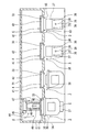
- the carrier block E1 will be further described with reference to the cross-sectional plan view of FIG. 2, the perspective view of FIG. 3, and the longitudinal side view of FIG.
- the carrier block E1 side and the interface block E3 side will be described as the rear side and the front side, respectively.
- the carrier block E1 includes a housing 31.
- the housing 31 delivers the carrier C to and from the carrier C transport mechanism, and delivers the wafer W between the carrier C and the coating and developing apparatus 1.
- the four load ports 3 are configured.
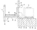
- Each load port 3 includes a stage (mounting unit) 32 on which the carrier C is placed, a transfer port 33 for the wafer W, and an open / close door 4 that opens and closes the transfer port 33 in addition to the housing 31.
- the A lower portion of the casing 31 protrudes rearward to form a stepped portion 34.
- the stages 32 of the load ports 3 are arranged in the lateral direction.
- the transfer port 33 is opened in the wall surface 35 of the housing 31 as viewed from the rear side of each stage 32.
- An annular recess 36 is formed along the outer edge of the transport port 33 in the wall surface 35.
- the stage 32 moves the carrier C between a retracted position shown by a chain line in FIG. 4 and an advanced position shown in FIG.
- reference numeral 37 denotes a moving mechanism for moving the stage 32 forward and backward.
- three support pins 38 for preventing the positional deviation of the carrier C on the stage 32 are provided protruding upward.
- reference numeral 39 denotes a hook that can protrude and retract on the surface of the stage 32.
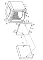
- the carrier C will be described with reference to the perspective view of FIG.
- the carrier C includes a container body 5 and a lid body 6 that is detachable from the container body 5.
- Each support portion 51 is configured as a slot 500 which is a storage area of the wafer W, and for example, 25 slots 500 are provided (in the drawings, less than 25 are shown for convenience).
- the slots 500 may be indicated by numbers 501, 502... 525 in order from the bottom to the top.
- a take-out port 52 for the wafer W is formed on the front surface of the container body 5, and the take-out port 52 is closed by the lid body 6.
- reference numeral 54 denotes an opening edge around the take-out port 52.
- An engagement groove 55 is formed on the inner peripheral side of the opening edge 54.
- a hole 56 is provided in the lower portion of the container body 5.
- rotating parts 61 are provided on the left and right sides, and linearly moving parts 62 extending vertically are provided above and below the rotating part 61.
- the rotating part 61 is provided with a key hole 63 into which a later-described latch key 43 is inserted, and the rotating part 61 is rotated by the rotation of the latch key 43 inserted into the key hole 63 as described above. Due to the rotation of the rotating part 61, the linearly moving part 62 is switched between a state in which the front end protrudes from the upper side and the lower side of the lid body 6 and a state in which it is drawn into the lid body 6. The front end of the linear movement portion 62 is engaged with the engagement groove 55 of the container body 5 in a state of protruding from the lid body 6, whereby the lid body 6 is locked to the container body 5.
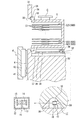
- one of the three support pins 38 of the stage 32 is surrounded by a dotted circle, drawn out and enlarged. However, the state where the support pin 38 is viewed from a direction different from that of the pull-out source is shown at the point of pull-out. As shown in these drawings, the side portion of the support pin 38 is notched, and the vibration sensor 11 is provided in the notch.
- this vibration sensor 11 for example, a known sensor is used. Specifically, for example, a device used as a bone conduction speaker or a bone conduction microphone that mutually converts a bone conduction sound and an electrical signal transmitted through a human skull can be used.
- the vibration sensor 11 is enlarged at the tip of a chain line arrow, and an outline of a vertical side surface thereof is shown.
- 12 is a housing
- 13 is a support portion provided in the housing 12.
- reference numeral 14 denotes a circular piezoelectric element whose central portion is supported by the support portion 13 and is made of, for example, piezoelectric ceramics.
- reference numeral 15 denotes a weight provided in a ring shape so as to surround the peripheral end of the piezoelectric element 14.
- the piezoelectric element 14 is deformed according to the vibration of the vibration sensor 11 to generate electric charges.
- An internal wiring (not shown) is formed in the housing 12 in order to transmit an electric signal (sensing signal) based on the charges to the outside of the housing 12.
- reference numeral 15 denotes a cable that is connected to the internal wiring and transmits the electrical signal to the control unit 2.
- the cable 15 is omitted in the drawings other than FIG. 3 for convenience.
- a layer 16 made of resin, for example, is provided outside the housing 12 (FIG. 5), and the layer 16 is in close contact with the support pins 38 and the housing 12.
- the container body 5 is in close contact with the support pins 38 when placed on the stage 32. Further, since the wafer W is supported in contact with the container main body 5, when a contact sound due to contact between the wafer W and the fork 48 is generated in the container main body 5 as will be described later, solids out of the contact sound are generated. Solid propagation sound, which is a longitudinal wave and a transverse wave conducted as a medium, propagates sequentially to the wafer W, the container body 5, the support pins 38, the layer 16, and the vibration sensor 11.
- the vibration sensor 11 vibrates by this solid propagation sound, and the signal according to this vibration is output.
- air-propagating sound which is longitudinal wave vibration that propagates using air as a medium
- solid-propagating sound is suppressed from being attenuated during propagation. Therefore, when the contact occurs, the vibration sensor 11 accurately outputs a signal corresponding to the contact sound. High output. Further, since the solid propagation sound propagates faster than the air propagation sound, when the contact sound is generated, the signal is quickly output from the vibration sensor 11.
- the open / close door 4 includes a door body 41 provided inside the housing 31.
- the door main body 41 is configured to be movable back and forth and up and down by a drive mechanism (not shown), and opens and closes the conveyance port 33 as shown in FIGS.
- the opening / closing door 4 includes a lid opening / closing mechanism 42 on the rear side of the door main body 41, and the lid opening / closing mechanism 42 includes a latch key 43 on the rear side thereof.
- the latch key 43 rotates around the horizontal axis. As the stage 32 advances and retreats, the latch key 43 is inserted into and extracted from the key hole 63 of the lid 6 of the carrier C placed on the stage 32.
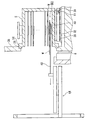
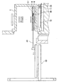
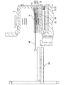
- a wafer transfer robot 44 shared by each load port 3 is provided in the casing 31.
- the transfer robot 44 includes an upright frame 45 that can move horizontally in the left-right direction, a lift 46 that is a lift mechanism that can be moved up and down on the frame 45, a base 47 that can rotate about the vertical axis on the lift 46, and A fork 48 is provided as a support body for the wafer W that can be moved back and forth on the base 47.
- the base 47 constitutes an advancing / retracting mechanism for advancing and retracting the fork.
- the fork 48 protrudes in parallel so that the tip portion is divided into two forks from the base, and is configured as a generally U-shaped flat plate in plan view, and supports the back surface of the wafer W to carry the wafer W.
- the fork 48 is made of ceramics, for example.
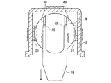
- FIG. 7 is a rear perspective view of the fork 48.
- a pin 49 that protrudes toward the back surface (lower surface) of the fork 48 is provided at each tip of the fork 48.
- the pin 49 is a sound amplifying unit for amplifying the contact sound between the fork 48 and the wafer W in order to detect friction between the back surface of the fork 48 and the surface of the wafer W supported by the slot 500 of the container body 5. It is configured as.
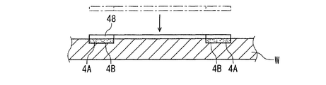
- FIGS. 8 and 9 show a fork 48 in which the pin 49 is not provided.
- FIG. 8 is a schematic view of the fork 48 and the wafer W viewed from the distal end side toward the proximal end side.
- FIG. 9 is a top view of the wafer W stored in the fork 48 and the container body 5.
- the fork 48 enters the container body 5 and delivers the wafer W, and then descends and retracts. There is a case where the wafer W is rubbed by contacting the surface of the wafer W located at the lower side during the lowering and moving backward in such a contact state.
- the air layer 4A is likely to be interposed between the back surface of the fork 48 and the front surface of the wafer W. 4A becomes a cushion, and the impact is attenuated when the fork 48 collides with the surface of the wafer W (FIG. 8). That is, due to the air layer 4 ⁇ / b> A, the solid propagation sound generated when the fork 48 and the wafer W collide with each other is reduced. Further, when the fork 48 moves backward and rubs against the wafer W, the fork 48 moves so as to slide on the air layer 4A sandwiched between the fork 48 and the surface of the wafer W. That is, a large frictional force is not generated between the fork 48 and the surface of the wafer W, and thus the generated solid propagation sound is small (FIG. 9). In the figure, 4B is a scratch on the wafer W due to rubbing.
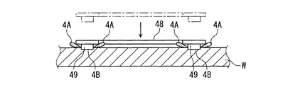
- FIG. 10 and 11 show a fork 48 provided with a pin 49.
- FIG. 10 shows a schematic view of the fork 48 and the wafer W as seen from the base end side as in FIG. 8, and
- FIG. 11 shows the top surface of the fork 48 and the wafer W as in FIG. Yes.
- the fork 48 descends and collides with the surface of the wafer W, the fork 48 moves so that the pins 49 tear the air layer 4A (FIG. 10). That is, compared with the case where the pin 49 is not provided, the shock attenuation by the air layer 4A is suppressed, and a large solid propagation sound is generated by the collision.
- the fork 48 moves backward in a state where the air layer 4A is suppressed from being sandwiched between the pins 48 and the surface of the wafer W, so that the pins 48 are placed on the surface of the wafer W in a state where slippage by the air layer 4A is suppressed. Rubbing generates a large solid propagation sound (FIG. 11).
- the material constituting the pin 49 when the fork 48 not provided with the pin 49 is in contact with the wafer W as described above, a larger solid propagation sound is generated than when the fork 48 is in contact with the wafer W.
- a material that can increase the output signal is selected. Specifically, for example, a relatively hard resin such as metal or polyether / ether / ketone is used as the material. When the above contact occurs, solid propagation sound of, for example, 500 Hz to 10,000 Hz is generated.
- the pin 49 is configured in such a size that the risk does not increase too much.
- the size L1 is about 100 ⁇ m. 4, 7, 10, 13-17, etc.
- the height of the pin 49 is shown larger than the actual size with respect to the thickness of the fork 48.
- the pin 49 is shown in the shape of a ring plate, but is not limited to such a shape.
- the pin 49 may be formed in a disc shape, a square plate shape, a vertically extending rod shape, or a horizontally extending rod shape. it can.
- the control unit 2 includes a program storage unit 21, a CPU 22, and a memory 23, and these are connected to a bus 24.
- the program storage unit 21 is configured by a computer storage medium such as a storage medium such as a flexible disk, a compact disk, a hard disk, an MO (magneto-optical disk), and a memory card.
- the program 25 stored in the storage medium is installed in the control unit 2 while being stored in such a storage medium.
- the program 25 transmits a control signal to each part of the coating / developing apparatus 1 to control its operation, transfer the wafer W, process the wafer W in each of the blocks E1 to E4, unload the wafer W from the carrier C, Instructions (steps) are incorporated so that each operation of loading the wafer W into the carrier C and detecting the friction between the wafer W and the fork 48 can be performed.
- the CPU 22 performs various calculations in order to output the control signal as described above.
- the vibration sensors 11 provided on the support pins 38 of the respective stages 32 are respectively connected to the control unit 2, and an output signal from the vibration sensor 11 is amplified by an amplification unit (not shown) provided in the control unit 2.
- the conversion unit converts the analog signal into a digital signal and outputs it to the bus 24.
- the memory 23 stores time series data (voltage data) of the voltage value of the output signal when the fork 48 moves forward and backward with respect to the container body 5 when the wafer W is stored in the container body 5.
- a Fourier transform unit 26 is connected to the bus 24.
- the Fourier transform unit 26 performs a Fourier transform on the voltage data to obtain a frequency spectrum shown later.
- an alarm output unit 27 is connected to the bus 24.
- the alarm output unit 27 outputs an alarm when it is determined that rubbing between the wafer W and the fork 48 has occurred. This alarm is a predetermined voice or screen display.
- FIG. 13 the carrier C is transported to the stage 32 of the load port 3 by the carrier transport mechanism in a state where a signal is output from the vibration sensor 11 of the load port 3 toward the control unit 2. At this time, the voltage value of the signal from the vibration sensor 11 is not written to the memory 23.
- the support pin 38 of the stage 32 is inserted into the hole 56 of the carrier C to which the substrate W is transferred, and the carrier C is placed on the stage 32 so as to be supported by the support pin 38, and the wall surface of the load port 3. Located in a retracted position away from 35. Thereafter, the stage 32 moves forward, the opening edge 54 of the carrier C enters the recess 36 of the wall surface 35, and the latch key 43 is inserted into the key hole 63 of the rotating portion 61. The latch key 43 is rotated, the engagement between the lid body 6 and the container body 5 is released, the lid body 6 is held by the lid body opening / closing mechanism 42 of the open / close door 4, and the door body 41 moves forward and then descends. To do. As a result, the lid 6 is removed from the container body 5 and the transfer port 33 of the load port 3 is opened.
- the fork 48 of the transfer robot 44 After the fork 48 of the transfer robot 44 is positioned at a predetermined height, the fork 48 moves forward so as to be positioned below the wafer W in the slot 501 of the container body 5, and ascends to support the back surface of the wafer W. Thereafter, the fork 48 moves backward to carry out the wafer W from the container body 5 (FIG. 13). The wafer W is transferred to the processing block E2. Thereafter, the transfer robot 44 transfers wafers W one by one to the processing block E2 in the same manner as the wafer W in the slot 501 in order from the lower slot 500.
- the wafer W transferred to the processing block E2 is transferred from the interface block E3 ⁇ the exposure apparatus E4 ⁇ the processing block E2, and then returned to the slot 500 where the wafer W was originally stored.
- the wafers W stored in the lower slot 500 are sequentially returned to the slot 500.
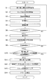
- the case where the wafer W in the slot 501 is completely stored in the container body 5 and the wafer W in the slot 502 and then the slot 503 is stored in the container body 5 will be described as an example. Reference is also made to the flowchart of FIG. 18 as appropriate.
- the fork 48 moves to a preset height position while holding the back surface of the wafer W unloaded from the slot 502.
- the fork 48 starts to advance toward the container body 5 (FIG. 14), and an IN-OUT signal indicating that the advance has started, that is, the delivery by the fork 48 has started, is sent from the transfer robot 44 to the control unit. 2 is output.
- the control unit 2 receives the IN-OUT signal (step S1), and starts writing the voltage data of the output signal from the vibration sensor 11 into the memory 23 (step S2).
- the fork 48 moves backward (FIG. 15).
- the fork 48 moves out of the container body 5 and is positioned at a predetermined position, the fork 48 is stopped from moving backward.
- a predetermined measurement time for example, 0.4 seconds has elapsed since the start of the storage of the voltage data (step S3)
- the writing of the voltage data is stopped (step S4).
- the timing at which the storage of the voltage data is stopped and the timing at which the retraction of the fork 48 stops are, for example, substantially simultaneously or simultaneously.
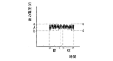
- FIG. 19 is a graph showing an example of voltage data stored in the memory 23 at the time of delivery to the slot 502, where time is set on the horizontal axis and voltage is set on the vertical axis. It is assumed that rubbing between the fork 48 and the wafer W has not occurred during delivery to the slot 502. Since the vibration sensor 11 vibrates due to the driving sound of the motor of the transfer robot 44, the voltage changes with time in the graph of FIG. Note that A in the graph is a predetermined voltage value.
- the control unit 2 detects the difference between the maximum value and the minimum value of the voltage (set as the first half side maximum amplitude) in the predetermined section R1. Further, a difference between the maximum value and the minimum value of the voltage (referred to as the latter half maximum amplitude) is detected in a predetermined section R2 after the section R1.
- the section R1 is a section in which the fork 48 advances in the container body 5.
- the section R ⁇ b> 2 is a section including the operation of lowering the fork 48 and retreating inside the container body 5.
- the control unit 2 calculates the second half maximum amplitude ⁇ the first half maximum amplitude (step S5), and determines whether or not the calculated value is within the allowable range (step S6).
- the first half maximum amplitude is (ab) and the second half maximum amplitude is (cd).
- the latter half maximum amplitude ⁇ first half maximum amplitude (cd) ⁇ (ab) It is within the allowable range.
- the fork 48 that has received the wafer W from the processing block E2 is positioned at a predetermined height. Thereafter, similarly to the transfer of the wafer W to the slot 502, the transfer of the wafer W to the next slot 503 is performed according to the above steps S1 to S6.
- the fork 48 holding the wafer W is moved forward (FIG. 16), the acquisition of the voltage data is started, the forward movement of the fork 48 is stopped, and the fork 48 is lowered by the set height to the support portion 51 of the slot 503.
- the wafer W is transferred. Thereafter, the fork 48 is retracted, the fork 48 is retracted, the acquisition of the voltage data is stopped, and the latter half maximum amplitude calculated from the obtained voltage data minus the first half maximum amplitude is within an allowable range. Is determined.
- the fork 48 is not rubbed against the wafer W in the container body 5 when the fork 48 moves forward.
- the fork 48 is lowered, as shown in FIG. 10, the back surface of the fork 48 collides with the surface of the wafer W in the slot 502 (FIG. 17). It is assumed that the surface of the wafer W is rubbed as described above.
- the solid propagation sound due to the collision and rubbing propagates to the vibration sensor 11 via the container body 5 and the support pin 38 of the stage 32, and an output signal corresponding to the solid propagation sound is output to the control unit 2. Is done.
- FIG. 20 is a graph showing an example of voltage data acquired when the wafer W is transferred to the slot 503 in the same manner as FIG. As described above, contact between the fork 48 and the wafer W in the slot 502 (collision and rubbing) occurs, and a loud noise is generated particularly when the pin 49 collides with the wafer W when the fork 48 is lowered.
- is larger than the maximum amplitude
- B is a predetermined voltage value.
- step S6 When it is determined in step S6 that it is out of the allowable range, the control unit 2 performs a Fourier transform on each of the voltage data sections R1 and R2 obtained by the delivery of the slot 503 to obtain a frequency spectrum (step S7).
- the upper side and the lower side of FIG. 21 are examples of frequency spectra obtained from the sections R1 and R2, respectively.
- the horizontal axis represents frequency
- the vertical axis represents voltage amplitude.
- the PSD is calculated by squaring the amplitude value of each frequency in the frequency range and dividing the sum of the squared values by the upper limit of the frequency range minus the lower limit of the frequency range, ie, 10000 Hz-500 Hz. Value. Assuming that the PSDs calculated from the first-half frequency spectrum and the second-half frequency spectrum are the first-half PSD and the second-half PSD, respectively, the control unit 2 calculates the second-side PSD-first-half PSD after calculating these PSDs (step S8). ), It is determined whether or not the calculated value is within an allowable range (step S9).
- the vibration sensor 11 also vibrates due to factors other than the rubbing between the wafer W and the fork 48.
- the other factors include, for example, the vibration sound of the motor that drives each part of the transfer robot 44 as described above, the driving sound of the module that processes the wafer W in the coating and developing apparatus 1, and the inside of the clean room. And driving sounds and warning sounds emitted from other semiconductor manufacturing apparatuses other than the developing apparatus 1.
- the sound generated by these other factors has a higher frequency than the contact sound between the wafer W and the fork 48.
- the amplitude in the frequency band higher than 10000 Hz in the frequency spectrum increases and the amplitude in the frequency band lower than 10000 Hz decreases.
- the amplitude in the frequency band lower than 10000 Hz increases in the frequency spectrum, and the amplitude in the frequency band higher than 10000 Hz decreases. That is, when the vibration sensor 11 vibrates due to the contact between the fork 48 and the wafer W, the latter half PSD-first half PSD becomes a relatively high value.
- the second half side PSD-first half side PSD has a relatively low value, so that the presence or absence of the contact can be identified.
- step S10 When not only the vibration sensor 11 of the stage 32 being transferred but also the vibration sensor 11 of another stage 32 that has not been transferred is detected at the same time, it is regarded as environmental noise and the contact between the fork and the substrate is actually detected. Judge that it is not happening.
- step S10 the calculated value of the second half side PSD ⁇ first half side PSD is out of the allowable range in step S9. Further, in step S10, it is confirmed that the same signal as the signal outside the allowable range is not detected from the stage that has not been delivered. Thereby, it is determined that the wafer W is rubbed by the fork 48 (step S11). Then, various data such as the time of delivery to the slot 503 and the voltage data acquired when the wafer W is delivered to the slot 503 are transmitted to the host computer and stored (step S12). Further, the transfer of the wafer W by the transfer robot 44 is stopped (step S13), and an alarm is output (step S14).
- each step S is also performed when the wafer W is delivered to the lowermost slot 501.
- the control unit 2 determines whether the rubbing is present based on the frequency spectrum obtained from each of the sections R1 and R2. Is judged. Also from this point, it is possible to prevent the erroneous detection from occurring. Moreover, since the control part 2 always monitors the signal from the vibration sensor 11 provided in each stage 32, even if environmental noise etc. which are not said rubbing arise for some reason, delivery is not performed. In other stages 32, it is possible to prevent erroneous detection by determining whether or not a similar signal is detected at the same time as the stage 32 in which delivery is performed.
- the transfer of the wafer W is stopped, but such a countermeasure is not limited.
- a case where it is determined that the rubbing has occurred when the wafer W is delivered to the slot 503 as described above will be described.
- the height position of the fork 48 when the wafer W is moved in the state where the wafer W is held when the wafer W is delivered to the slot 503 is the slot 503 entry height position
- the height set in advance from the slot 503 entry height position is set.
- the fork 48 is located at a height position shifted downward. Thereafter, the fork 48 is advanced by a predetermined amount, and the tip thereof is positioned between the wafers W of the slots 502 and 503 (FIG. 22).
- the control unit 2 monitors the change in the output signal from the vibration sensor 11 while raising the fork 48.
- the height position of the fork 48 is stored and the ascent of the fork 48 is stopped.
- the control unit 2 monitors the change in the output signal while lowering the fork 48.
- a collision between the surface of the wafer W in the slot 502 and the fork 48 occurs and the voltage of the output signal increases, the height position of the fork 48 is stored and the lowering of the fork 48 is stopped (FIG. 23).
- control unit 2 calculates an intermediate height position between the stored height positions, and determines the intermediate height position as a height position when the fork 48 moves backward. Then, the position where the predetermined height is separated from the determined height position is set as the slot 503 entry height position, and the entry height position is corrected.
- the wafer W is transferred to the slots 504 to 525 according to the above steps S1 to S11. That is, in this example, even if the rubbing between the wafer W and the fork 48 is detected, the operation of the transfer robot 44 in step S12 is not stopped. Then, after storing the wafer W in the slots 504 to 525, the carrier C is unloaded from the stage 32, and the subsequent carrier C is transferred to the stage 32. When the wafer W is discharged from the subsequent carrier C and then stored in the slot 503 of the carrier C, the fork 48 holding the wafer W is positioned at the corrected slot 503 entry height position. Then move forward. Thereafter, the fork 48 moves backward at the intermediate height position, so that the rubbing between the fork 48 and the wafer W in the slot 502 is prevented.
- the time for adjusting the height position can be shortened.
- the time can be shortened from when the rubbing is detected until the operation of the coating and developing apparatus 1 is resumed.
- the pins 49 are provided only on the back surface of the fork 48 as in the above embodiment. However, in order to accurately detect the height position of the fork 48 contacting the wafer W, the pins 49 are also provided on the front surface. Is preferably provided.
- the pins 49 are not limited to be provided.
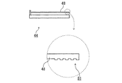
- the fore 48 in FIG. 24 has a rough front end and is configured as an uneven portion 81 in which minute unevenness is formed.
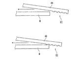
- the fork 48 is provided horizontally on the transport robot 44, but its tip is slightly inclined due to gravity.
- FIG. 25 shows a state in which the concave and convex portion 81 of the fork 48 whose tip is inclined in this manner rubs the corner portion of the wafer W when the fork 48 moves backward.
- the inclination of the fork 48 is shown larger than the actual inclination.
- the concavo-convex portion 81 when the wafer W is rubbed by the concavo-convex portion 81, a larger amount of energy is generated than when the flat fork 48 rubs the wafer W. That is, the uneven portion 81 can generate a relatively large frictional sound. In order to discriminate between the vibration of the vibration sensor 11 due to the other factors described above and the vibration of the vibration sensor 11 due to the friction with the wafer W, the friction causes the solid propagation sound having a frequency of, for example, 500 to 10000 Hz to be generated.
- the concavo-convex portion 81 is configured so as to be rough.
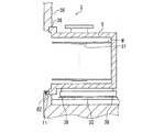
- FIG. 26 shows an example in which the pins 49 are provided on the surface of the fork 48.
- the vibration sensor 11 is not limited to being provided on the stage 32, as long as it is provided at a position where solid propagation sound propagating through the container body 5 can be detected.
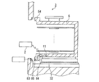
- FIG. 27 shows an example in which the vibration sensor 11 is provided in the recess 36 of the wall surface 35 of the load port 3.
- a spring 82 as an urging portion is provided on the front side of the vibration sensor 11, and when the wafer W is delivered to the container body 5, the vibration sensor 11 is urged rearward by the spring 82, The vibration sensor 11 is configured to be in close contact with the container body 5 to detect the solid propagation sound more reliably.
- the spring 82 may not be provided if the wafer W is transferred by moving the opening edge 54 of the container body 5 to a position where the opening edge 54 is in close contact with the vibration sensor 11.
- the vibration sensor 11 may be provided in the container body 5.
- the vibration sensor 11 is embedded in the opening edge 54, and the surface of the vibration sensor 11 is exposed. Further, an electrode (not shown) for taking out an output signal obtained from the piezoelectric element 14 is provided on the exposed surface.
- An electrode 83 is embedded in the recess 36 of the load port 3. When the opening edge 54 enters the recess 36 in order to deliver the wafer W between the container body 5 and the transfer robot 44, the electrode of the vibration sensor 11 and the electrode 83 are connected. The vibration sensor 11 is connected to the control unit 2 via the electrode 83 so that an output signal from the vibration sensor 11 can be supplied to the control unit 2.
- FIG. 29 shows a configuration example of another container body 5 and load port 3.
- the vibration sensor 11 and the wireless transmission unit 84 are embedded.
- the wireless transmitter 84 is connected to the electrode 85 exposed on the surface of the opening edge 54.
- a power supply unit 86 is connected to the electrode 83 of the recess 36 instead of the control unit 2.
- the electrodes 83 and 85 are connected to each other, and power is supplied to the wireless transmission unit 84.
- the wireless transmission unit 84 is configured to convert the analog output of the vibration sensor 11 into digital data and wirelessly transmit it to the control unit 2.
- the control unit 2 constantly monitors each vibration sensor 11 to prevent erroneous detection due to environmental noise. Can do.
- the present invention is not limited to detecting the rubbing between the wafer W and the fork 48 of the container body 5.
- a vertical heat treatment apparatus that carries the wafers W held by a holder that holds a large number of wafers W arranged in a shelf shape up and down in a heating furnace together with the wafer boat and heats them in a lump.
- the wafer W is transferred between the wafer boat placed on the stage and the carrier C by a transfer robot similar to the transfer robot 44.
- a pin 49 and an uneven portion 81 are provided on the fork 48 of the transfer robot, and a vibration sensor 11 is provided so that, for example, solid propagation sound is propagated from the wafer boat to the stage.
- the control unit 2 Based on the output from the vibration sensor 11, the control unit 2 can detect rubbing between the wafer W held on the wafer boat and the fork 48.
- the lifting platform 47 of the transfer robot 44 is moved up and down to transfer the wafer W to the container body 5.
- the stage 32 is moved up and down to transfer the wafer W. Also good. Even with such a configuration, rubbing between the wafer W and the fork 48 can be detected.
- the delivery of the wafer W to the container body 5 includes at least one of the case where the wafer W is transferred to the container body 5 and the case where the wafer W is received from the container body 5. That is, the apparatus may be configured such that only one of the transfer of the wafer W to the container body 5 and the transfer of the wafer W from the container body 5 is performed.
- Evaluation test 1 An evaluation test conducted in connection with the present invention will be described.
- the fork 48 is repeatedly entered, lowered, and retracted in order with respect to the container body 5 in which the wafer W is stored, and is provided on the stage 32 as described above.
- the voltage output from the vibration sensor 11 was measured.
- a pin 49 which is a metal washer, is provided on the back surface of the fork 48, as in the above embodiment.
- the height of the fork 48 was set so that the fork 48 and the wafer W of the container body 5 were not rubbed when the fork 48 was retracted.
- the fork 48 passes 33 ⁇ m, 66 ⁇ m, and 99 ⁇ m below the surface of the wafer W stored in the container body 5, respectively. That is, the height of the fork 48 is set so that the wafer W is rubbed when retreating.
- the height of the fork 48 is set so that contact with the wafer W does not occur when the fork 48 moves forward.
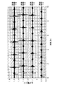
- FIG. 30 is a graph showing the results obtained in the evaluation tests 1-1 to 1-4.
- the horizontal axis of the graph indicates the time (unit: second) that has elapsed since the start of each evaluation test.
- the vertical axis represents the output voltage (unit: V).
- the voltage change during the repetitive operation of the fork 48 of the fork 48 in each evaluation test is shown, and the timing at which the first fork 48 starts to advance in the displayed range is expressed as IN. It is described as.
- the evaluation test 1-1 after a small frequency variation occurs, a similar frequency variation occurs again after a while, and these frequency variations are repeated. These frequency fluctuations are due to the operation sound of the transfer robot 44 when the fork 48 enters and retracts, respectively. From this graph, it can be seen that the maximum amplitude on the first half side and the maximum amplitude on the second half side described in the embodiment are almost the same.
- Evaluation test 2 The operation of storing the wafer W in the container body 5 by moving the fork 48 back and forth was performed, and the voltage output from the vibration sensor 11 was measured during that time.
- the pin 49 is not provided on the fork 48.
- the height of the fork 48 is set so that the wafer W is rubbed when the storage operation is performed.
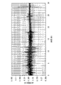
- FIG. 31 is a graph showing the results of this evaluation test 2.
- the horizontal and vertical axes of the graph indicate time and output voltage, respectively, as in FIG. 30 of evaluation test 1.
- the vertical axis of the graph of FIG. 30 is graduated every 0.1 V and scale lines are shown in the graph, and auxiliary scale lines are shown in increments of 20 mV between the scale lines.
- the vertical axis of the graph of FIG. 31 in this evaluation test 2 is marked with a scale every 5 mV, and scale lines are shown in the graph, and auxiliary scale lines are shown in 1 mV increments between the scale lines.
- the output voltage fluctuates with a large width from the start of measurement to the end of measurement.
- Evaluation test 3-1 When the noise around the coating and developing apparatus 1 is large, even if the fork 48 has a sound amplifying part (protrusion), the contact sound between the wafer W and the fork 48 is buried in the noise component. It may end up. Therefore, predetermined intervals R1 and R2 are set for the voltage data acquired in the above-described evaluation test 1-3, and the first half frequency spectrum and the second half frequency spectrum in each of the intervals R1 and R2 described in the embodiment are respectively set. Asked. FIG. 32 shows the first half spectrum and the second half spectrum, respectively. When these frequency spectra are compared, it can be seen that the amplitude in the range of 500 Hz to 10,000 Hz is particularly changed.
- the frequency spectrum is calculated and a specific wavelength (in this case 500) is calculated.
- the presence or absence of rubbing of the wafer W can be determined by using the spectral intensity of ⁇ 10000 Hz.
- the difference between the first half frequency spectrum and the second half frequency spectrum for the amplitude exceeding 10,000 Hz is small because the wavelength of 10000 Hz is mainly due to high frequency components such as driving sound of surrounding structures. This is considered to be due to the fact that there are many things, and those due to components based on contact between the wafer W and the fork 48 are small.
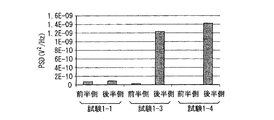
- Evaluation test 3-2 From the voltage data acquired in the evaluation tests 1-1, 1-3, and 1-4, the first-half PSD and the second-half PSD described in the embodiment were calculated. These PSDs are calculated for a frequency of 500 to 10000 Hz as in the embodiment. Further, the latter half PSD-first half PSD was calculated.
- the graph of FIG. 33 shows the first half PSD and the second half PSD of the evaluation tests 1-1, 1-3, and 1-4, and the graph of FIG. 34 shows the second half PSD of the evaluation tests—the first half PSD. Yes. From the graph of FIG. 34, it can be seen that the latter half PSD-first half PSD in the evaluation tests 1-3, 1-4 shows a larger value than the second half PSD-first half PSD in the evaluation test 1-1. From the results of these evaluation tests 3-1, 3-2, it can be seen that the presence or absence of rubbing can be determined using the frequency spectrum.
Landscapes
- Container, Conveyance, Adherence, Positioning, Of Wafer (AREA)
- Engineering & Computer Science (AREA)
- Robotics (AREA)
Abstract
Description
前記基板の下面を支持する支持体、及び前記支持体を進退させる進退機構を備え、前記載置部に載置された基板保持具に対して基板の受け渡しを行うための基板搬送機構と、
前記支持体を前記基板保持具に対して相対的に昇降させる昇降機構と、
前記基板保持具に保持された基板と前記支持体との接触により発生する接触音を増幅させるための音増幅部と、
前記基板保持具を伝播する固体伝播音を感知して感知信号を出力する振動センサからの前記感知信号に基づいて、前記基板と前記支持体との擦れを検出するための検出部と、
を備えることを特徴とする。
また、制御部2は、上記のように取得された区間R1、R2の電圧の最大振幅の差が異常になったときは、各区間R1、R2から求める周波数スペクトルに基づいて、前記擦れの有無を判定している。この点からも、上記の誤検出が起きることを防ぐことができる。また、制御部2は、各ステージ32に設けられる振動センサ11からの信号を常時監視しているので、たとえ何らかの理由により、前記擦れではない環境ノイズなどが生じても、受け渡しの行われていない他のステージ32において、受け渡しの行われているステージ32と同時に同様の信号検出されたかどうか判定することで、誤検出が起きることを防ぐことができる。
評価試験1
本発明に関連して行われた評価試験について説明する。評価試験1では、上記の搬送ロボット44を用い、フォーク48をウエハWが格納された容器本体5に対して進入、下降及び後退動作を順に繰り返し行い、その間に上記のようにステージ32に設けた振動センサ11から出力される電圧を測定した。前記進入、下降及び後退動作を複数回繰り返し行うと、進入時の高さ及び後退時の高さを変更して、再度進入、下降及び後退動作を繰り返し行った。前記フォーク48の裏面には、上記の実施形態と同様に、金属のワッシャであるピン49が設けられている。
フォーク48の進退による容器本体5へのウエハWの格納動作を行い、その間に振動センサ11から出力される電圧を測定した。この評価試験2ではフォーク48にピン49を設けていない。この格納動作が行われているときに、ウエハWの擦れが起きるようにフォーク48の高さが設定されている。
塗布、現像装置1の周囲のノイズが大きい場合には、フォーク48に音増幅部(突起)を有している場合であっても、ウエハWとフォーク48との接触音がノイズ成分に埋もれてしまう事がある。そこで、上記の評価試験1-3において取得された電圧データについて、所定の区間R1、R2を設定し、実施の形態で説明した各区間R1、R2における前半側周波数スペクトル、後半側周波数スペクトルを夫々求めた。図32はこれら前半側スペクトル、後半側スペクトルを夫々示している。これら周波数スペクトルを比較すると、500Hz~10000Hzにおける振幅が特に変化していることが分かる。
上記の評価試験1-1、1-3、1-4において取得された電圧データから、実施の形態で説明した前半側PSD、後半側PSDを夫々算出した。これらPSDは、実施の形態と同様に500~10000Hzの周波数について算出している。また、後半側PSD-前半側PSDを演算した。図33のグラフは評価試験1-1、1-3、1-4の前半側PSD及び後半側PSDを示し、図34のグラフは、これら各評価試験の後半側PSD-前半側PSDを示している。図34のグラフより評価試験1-3、1-4における後半側PSD-前半側PSDは、評価試験1-1における後半側PSD-前半側PSDよりも大きい値を示していることが分かる。これら評価試験3-1、3-2の結果から、周波数スペクトルを用いて、擦れの有無の判定を行えることが分かる。
C キャリア
W ウエハ
1 塗布、現像装置
11 振動センサ
2 制御部
3 ロードポート
38 支持ピン
44 搬送ロボット
48 フォーク
49 ピン
5 容器本体
81 凹凸部
Claims (10)
- 複数の基板を棚状に保持するための基板保持具が載置される載置部と、
前記基板の下面を支持する支持体、及び前記支持体を進退させる進退機構を備え、前記載置部に載置された基板保持具に対して基板の受け渡しを行うための基板搬送機構と、
前記支持体を前記基板保持具に対して相対的に昇降させる昇降機構と、
前記基板保持具に保持された基板と前記支持体との接触により発生する接触音を増幅させるための音増幅部と、
前記基板保持具を伝播する固体伝播音を感知して感知信号を出力する振動センサからの前記感知信号に基づいて、前記基板と前記支持体との擦れを検出するための検出部と、
を備えることを特徴とする基板搬送装置。 - 前記音増幅部は、前記支持体に設けられることを特徴とする請求項1記載の基板搬送装置。
- 前記検出部は、前記振動センサからの感知信号に基づいて得られる周波数スペクトルに基づいて、前記基板と前記支持体との擦れを検出することを特徴とする請求項1記載の基板搬送装置。
- 前記音増幅部は、基板と支持体との間の空気層による前記接触音の低下を防ぐための突部により構成されることを特徴とする請求項1記載の基板搬送装置。
- 前記音増幅部は、基板の端部との接触による接触音を増幅させるための凹凸部により構成されることを特徴とする請求項1記載の基板搬送装置。
- 前記振動センサを前記載置部に備えることを特徴とする請求項1記載の基板搬送装置。
- 前記基板保持具と基板搬送機構との間で基板を受け渡すための搬送口が形成された隔壁が設けられ、
当該隔壁に前記振動センサを備えることを特徴とする請求項1記載の基板搬送装置。 - 前記振動センサを前記載置部に載置された基板保持具に向けて付勢する付勢部が、前記隔壁に設けられることを特徴とする請求項7記載の基板搬送装置。
- 前記基板搬送装置は、前記載置部を複数備えるとともに、複数の前記載置部にそれぞれ対応する複数の前記振動センサを有し、
前記検出部は、複数の前記載置部にそれぞれ対応する複数の前記振動センサのうち、基板搬送中の前記載置部に対応する前記振動センサと、基板搬送中でない少なく1つの前記載置部に対応する前記振動センサとから、前記感知信号が同時に出力された場合、前記基板と前記支持体との擦れではないと判定することを特徴とする請求項1記載の基板搬送装置。 - 前記検出部により前記基板と支持体との擦れが検出されたときに、前記検出部は後に基板保持具に対して基板の受け渡しを行うときの前記支持体の高さが補正されるように、前記昇降機構の動作を制御することを特徴とする請求項1記載の基板搬送装置。
Priority Applications (3)
| Application Number | Priority Date | Filing Date | Title |
|---|---|---|---|
| KR1020157018890A KR102077363B1 (ko) | 2013-02-04 | 2014-01-31 | 기판 반송 장치 |
| US14/759,824 US9953853B2 (en) | 2013-02-04 | 2014-01-31 | Substrate transport apparatus |
| CN201480007436.1A CN104969339B (zh) | 2013-02-04 | 2014-01-31 | 基板输送装置 |
Applications Claiming Priority (2)
| Application Number | Priority Date | Filing Date | Title |
|---|---|---|---|
| JP2013-019580 | 2013-02-04 | ||
| JP2013019580A JP6044373B2 (ja) | 2013-02-04 | 2013-02-04 | 基板搬送装置 |
Publications (1)
| Publication Number | Publication Date |
|---|---|
| WO2014119740A1 true WO2014119740A1 (ja) | 2014-08-07 |
Family
ID=51262437
Family Applications (1)
| Application Number | Title | Priority Date | Filing Date |
|---|---|---|---|
| PCT/JP2014/052305 Ceased WO2014119740A1 (ja) | 2013-02-04 | 2014-01-31 | 基板搬送装置 |
Country Status (6)
| Country | Link |
|---|---|
| US (1) | US9953853B2 (ja) |
| JP (1) | JP6044373B2 (ja) |
| KR (1) | KR102077363B1 (ja) |
| CN (1) | CN104969339B (ja) |
| TW (1) | TWI567858B (ja) |
| WO (1) | WO2014119740A1 (ja) |
Cited By (1)
| Publication number | Priority date | Publication date | Assignee | Title |
|---|---|---|---|---|
| TWI918420B (zh) | 2024-03-25 | 2026-03-11 | 日商斯庫林集團股份有限公司 | 基板處理裝置及基板處理裝置之控制方法 |
Families Citing this family (19)
| Publication number | Priority date | Publication date | Assignee | Title |
|---|---|---|---|---|
| JP3025523B2 (ja) | 1990-10-15 | 2000-03-27 | 電気興業株式会社 | 高周波焼入れ装置用コイル自動交換装置 |
| US9791849B2 (en) * | 2015-05-26 | 2017-10-17 | GlobalFoundries, Inc. | Defect detection process in a semiconductor manufacturing environment |
| US9978631B2 (en) * | 2015-12-31 | 2018-05-22 | Beijing Naura Microelectronics Equipment Co., Ltd. | Wafer pick-and-place method and system |
| KR102397110B1 (ko) * | 2016-06-13 | 2022-05-12 | 도쿄엘렉트론가부시키가이샤 | 기판 반송 장치 및 기판 반송 방법 |
| JP6545396B2 (ja) * | 2016-09-29 | 2019-07-17 | 株式会社Kokusai Electric | 基板処理装置、振動検出システム及びプログラム |
| US10872793B2 (en) | 2017-11-10 | 2020-12-22 | Taiwan Semiconductor Manufacturing Co., Ltd. | System and method for monitoring operation conditions of semiconductor manufacturing apparatus |
| US10879095B2 (en) * | 2018-02-26 | 2020-12-29 | Samsung Electronics Co., Ltd. | Jig for evaluating semiconductor processing chamber |
| CN110504186B (zh) * | 2018-05-16 | 2022-01-18 | 台湾积体电路制造股份有限公司 | 半导体制造机台的状况监控方法及半导体制造系统 |
| US10533852B1 (en) * | 2018-09-27 | 2020-01-14 | Taiwan Semiconductor Manufacturing Company, Ltd. | Leveling sensor, load port including the same, and method of leveling a load port |
| JP7256360B2 (ja) * | 2018-12-14 | 2023-04-12 | シンフォニアテクノロジー株式会社 | 搬送異常検知システム |
| CN114466728B (zh) * | 2019-07-26 | 2025-05-27 | 朗姆研究公司 | 用于自动化晶片搬运机械手教导与健康检查的整合适应性定位系统及例程 |
| JP6983206B2 (ja) * | 2019-10-15 | 2021-12-17 | 株式会社アルバック | 基板搬送装置、および、基板搬送方法 |
| JP7288486B2 (ja) * | 2021-09-17 | 2023-06-07 | 株式会社Kokusai Electric | 基板処理方法、基板処理装置、半導体装置の製造方法、及びプログラム |
| CN114295735A (zh) * | 2021-12-09 | 2022-04-08 | 北京京仪自动化装备技术股份有限公司 | 晶圆传送系统的检测方法及晶圆传送系统 |
| CN114295199A (zh) * | 2021-12-09 | 2022-04-08 | 北京京仪自动化装备技术股份有限公司 | 一种晶圆传送系统检测方法及晶圆传送系统 |
| CN113899446B (zh) * | 2021-12-09 | 2022-03-22 | 北京京仪自动化装备技术股份有限公司 | 晶圆传送系统检测方法及晶圆传送系统 |
| JP7699556B2 (ja) * | 2022-02-08 | 2025-06-27 | 三菱電機株式会社 | 半導体製造装置および半導体装置の製造方法 |
| JP2026065327A (ja) * | 2024-10-03 | 2026-04-15 | 株式会社Screenホールディングス | 基板搬送装置および基板搬送方法 |
| JP2026065330A (ja) * | 2024-10-03 | 2026-04-15 | 株式会社Screenホールディングス | 基板搬送装置および基板搬送方法 |
Citations (6)
| Publication number | Priority date | Publication date | Assignee | Title |
|---|---|---|---|---|
| JP2000056819A (ja) * | 1998-07-07 | 2000-02-25 | Texas Instr Inc <Ti> | ロボット破壊センサシステム |
| JP2002009126A (ja) * | 2000-06-02 | 2002-01-11 | Samsung Electronics Co Ltd | ウェーハ移送装置及びウェーハ積載装備 |
| JP2004172287A (ja) * | 2002-11-19 | 2004-06-17 | Fujitsu Ltd | ウェハキャリア、検査用ウェハおよびウェハキャリアへのウェハ挿入調整方法 |
| JP2005254921A (ja) * | 2004-03-10 | 2005-09-22 | Denso Corp | 車両用乗員保護装置 |
| JP2010245476A (ja) * | 2009-04-10 | 2010-10-28 | Disco Abrasive Syst Ltd | ウエーハ加工装置 |
| JP2012249228A (ja) * | 2011-05-31 | 2012-12-13 | Nikon Corp | 電子装置、情報交換システム、通信相手特定方法および通信相手特定プログラム |
Family Cites Families (10)
| Publication number | Priority date | Publication date | Assignee | Title |
|---|---|---|---|---|
| US6473157B2 (en) * | 1992-02-07 | 2002-10-29 | Nikon Corporation | Method of manufacturing exposure apparatus and method for exposing a pattern on a mask onto a substrate |
| JPH05304198A (ja) * | 1992-04-27 | 1993-11-16 | Tel Varian Ltd | 搬送装置 |
| US20060215347A1 (en) | 2005-03-28 | 2006-09-28 | Tokyo Electron Limited | Processing apparatus and recording medium |
| JP2006278396A (ja) | 2005-03-28 | 2006-10-12 | Tokyo Electron Ltd | 処理装置及びプログラム |
| US7712370B2 (en) * | 2006-12-22 | 2010-05-11 | Asm Japan K.K. | Method of detecting occurrence of sticking of substrate |
| CN101546806A (zh) * | 2008-03-28 | 2009-09-30 | 松下电器产业株式会社 | 传感器器件及其制造方法 |
| US7750819B2 (en) * | 2008-04-07 | 2010-07-06 | Tech Semiconductor Singapore Pte Ltd | Real-time detection of wafer shift/slide in a chamber |
| WO2010010688A1 (ja) * | 2008-07-24 | 2010-01-28 | 株式会社アルバック | 処理装置の作動監視システム |
| JP5557516B2 (ja) * | 2009-12-09 | 2014-07-23 | 株式会社日立ハイテクノロジーズ | 真空処理装置 |
| CN201868400U (zh) * | 2010-11-03 | 2011-06-15 | 颀中科技(苏州)有限公司 | 晶圆转送台的防撞报警装置 |
-
2013
- 2013-02-04 JP JP2013019580A patent/JP6044373B2/ja active Active
-
2014
- 2014-01-28 TW TW103103252A patent/TWI567858B/zh active
- 2014-01-31 KR KR1020157018890A patent/KR102077363B1/ko active Active
- 2014-01-31 WO PCT/JP2014/052305 patent/WO2014119740A1/ja not_active Ceased
- 2014-01-31 US US14/759,824 patent/US9953853B2/en active Active
- 2014-01-31 CN CN201480007436.1A patent/CN104969339B/zh active Active
Patent Citations (6)
| Publication number | Priority date | Publication date | Assignee | Title |
|---|---|---|---|---|
| JP2000056819A (ja) * | 1998-07-07 | 2000-02-25 | Texas Instr Inc <Ti> | ロボット破壊センサシステム |
| JP2002009126A (ja) * | 2000-06-02 | 2002-01-11 | Samsung Electronics Co Ltd | ウェーハ移送装置及びウェーハ積載装備 |
| JP2004172287A (ja) * | 2002-11-19 | 2004-06-17 | Fujitsu Ltd | ウェハキャリア、検査用ウェハおよびウェハキャリアへのウェハ挿入調整方法 |
| JP2005254921A (ja) * | 2004-03-10 | 2005-09-22 | Denso Corp | 車両用乗員保護装置 |
| JP2010245476A (ja) * | 2009-04-10 | 2010-10-28 | Disco Abrasive Syst Ltd | ウエーハ加工装置 |
| JP2012249228A (ja) * | 2011-05-31 | 2012-12-13 | Nikon Corp | 電子装置、情報交換システム、通信相手特定方法および通信相手特定プログラム |
Cited By (1)
| Publication number | Priority date | Publication date | Assignee | Title |
|---|---|---|---|---|
| TWI918420B (zh) | 2024-03-25 | 2026-03-11 | 日商斯庫林集團股份有限公司 | 基板處理裝置及基板處理裝置之控制方法 |
Also Published As
| Publication number | Publication date |
|---|---|
| KR20150115734A (ko) | 2015-10-14 |
| JP2014150227A (ja) | 2014-08-21 |
| TW201444012A (zh) | 2014-11-16 |
| TWI567858B (zh) | 2017-01-21 |
| CN104969339B (zh) | 2017-06-06 |
| KR102077363B1 (ko) | 2020-02-13 |
| CN104969339A (zh) | 2015-10-07 |
| US9953853B2 (en) | 2018-04-24 |
| JP6044373B2 (ja) | 2016-12-14 |
| US20150340258A1 (en) | 2015-11-26 |
Similar Documents
| Publication | Publication Date | Title |
|---|---|---|
| JP6044373B2 (ja) | 基板搬送装置 | |
| JP7842264B2 (ja) | 基板貼り合わせ装置および基板貼り合わせ方法 | |
| JP7663367B2 (ja) | 基板処理装置および基板処理方法 | |
| KR101245464B1 (ko) | 열처리 장치, 열처리 방법 및 기억 매체 | |
| TWI445651B (zh) | 感測器單元、器械、導軌系統、倉儲系統及管理倉儲之方法 | |
| CN104781631B (zh) | 钢板的氧化皮厚度测量装置 | |
| JP2015116637A (ja) | 研削方法 | |
| JP6971383B2 (ja) | 基板処理装置、反応管形状測定方法及び半導体装置の製造方法 | |
| KR101967082B1 (ko) | 타이어 검사 장치, 및 타이어의 자세 검출 방법 | |
| JP2007083131A (ja) | 塗布装置及び塗布方法 | |
| KR102052216B1 (ko) | 액 처리 장치 및 액 처리 장치에 사용되는 프로그램을 기록한 컴퓨터로 판독 가능한 기록 매체 | |
| TWI524426B (zh) | 雷射處理裝置 | |
| JP4091378B2 (ja) | 基板処理装置 | |
| JP2007184564A (ja) | 基板処理装置における被測定物の物理量測定方法及び記憶媒体 | |
| CN113433797B (zh) | 基片处理装置和基片处理方法 | |
| JP2010201546A (ja) | 欠陥修正方法及び装置 | |
| KR102647252B1 (ko) | 액적을 검사하기 위한 장치 및 방법 | |
| KR102394037B1 (ko) | 테스팅 웨이퍼를 이용하여 웨이퍼 카세트로 진입하는 공정 웨이퍼의 위치 판단 방법 | |
| TWI492308B (zh) | 雷射處理裝置及其控制方法 | |
| JP7558711B2 (ja) | 搬送装置、及び、搬送方法 | |
| TWM673285U (zh) | 用於foup的檢測設備 | |
| JP2010287663A (ja) | 基板搬送装置 | |
| CN103170729A (zh) | 激光处理装置及其控制方法 | |
| JPH02305449A (ja) | ウェーハ枚数計数装置 |
Legal Events
| Date | Code | Title | Description |
|---|---|---|---|
| 121 | Ep: the epo has been informed by wipo that ep was designated in this application |
Ref document number: 14745402 Country of ref document: EP Kind code of ref document: A1 |
|
| WWE | Wipo information: entry into national phase |
Ref document number: 14759824 Country of ref document: US |
|
| ENP | Entry into the national phase |
Ref document number: 20157018890 Country of ref document: KR Kind code of ref document: A |
|
| NENP | Non-entry into the national phase |
Ref country code: DE |
|
| 122 | Ep: pct application non-entry in european phase |
Ref document number: 14745402 Country of ref document: EP Kind code of ref document: A1 |