WO2014115743A1 - 発光材料およびそれを用いた有機発光素子 - Google Patents
発光材料およびそれを用いた有機発光素子 Download PDFInfo
- Publication number
- WO2014115743A1 WO2014115743A1 PCT/JP2014/051184 JP2014051184W WO2014115743A1 WO 2014115743 A1 WO2014115743 A1 WO 2014115743A1 JP 2014051184 W JP2014051184 W JP 2014051184W WO 2014115743 A1 WO2014115743 A1 WO 2014115743A1
- Authority
- WO
- WIPO (PCT)
- Prior art keywords
- group
- substituted
- unsubstituted
- general formula
- integer
- Prior art date
Links
- 0 C1=CC=C*1c1cc(-c2c(*3c4cc(-c5cc(*6c7ccc(*8C=CC=C8)cc7-c7c6cccc7)ccc5*5c(cc6)ccc6-c6**(-c7ccccc7)*c(-c7ccccc7)*6)c5cc4)cccc2)c3cc1 Chemical compound C1=CC=C*1c1cc(-c2c(*3c4cc(-c5cc(*6c7ccc(*8C=CC=C8)cc7-c7c6cccc7)ccc5*5c(cc6)ccc6-c6**(-c7ccccc7)*c(-c7ccccc7)*6)c5cc4)cccc2)c3cc1 0.000 description 3
- OPKWTNCBQZAFLE-UHFFFAOYSA-N C(C1)C11C(c2ccccc2)=NC(c(cc2)ccc2-[n](c(cccc2)c2c2c3)c2ccc3-[n]2c3cc(C4CCCCC4)ccc3c3c2cc(C2CCCCC2)cc3)=NC(c2ccccc2)=C1 Chemical compound C(C1)C11C(c2ccccc2)=NC(c(cc2)ccc2-[n](c(cccc2)c2c2c3)c2ccc3-[n]2c3cc(C4CCCCC4)ccc3c3c2cc(C2CCCCC2)cc3)=NC(c2ccccc2)=C1 OPKWTNCBQZAFLE-UHFFFAOYSA-N 0.000 description 1
- SUVDEXXQEVHKTH-UHFFFAOYSA-N C(CC1)CCC1c(cc1c2cc(C3CCCCC3)ccc22)ccc1[n]2-c(cc1c2c3cccc2)ccc1[n]3-c(cc1)ccc1-c1nc(-c2ccccc2)nc(-c2ccccc2)n1 Chemical compound C(CC1)CCC1c(cc1c2cc(C3CCCCC3)ccc22)ccc1[n]2-c(cc1c2c3cccc2)ccc1[n]3-c(cc1)ccc1-c1nc(-c2ccccc2)nc(-c2ccccc2)n1 SUVDEXXQEVHKTH-UHFFFAOYSA-N 0.000 description 1
- CUNRCBBBPBWPTM-UHFFFAOYSA-N c(cc1)ccc1-c1nc(-c(cc2)ccc2-[n]2c3ccccc3c3c2cccc3)nc(-c2ccccc2)n1 Chemical compound c(cc1)ccc1-c1nc(-c(cc2)ccc2-[n]2c3ccccc3c3c2cccc3)nc(-c2ccccc2)n1 CUNRCBBBPBWPTM-UHFFFAOYSA-N 0.000 description 1
Images


Classifications
-
- C—CHEMISTRY; METALLURGY
- C07—ORGANIC CHEMISTRY
- C07D—HETEROCYCLIC COMPOUNDS
- C07D403/00—Heterocyclic compounds containing two or more hetero rings, having nitrogen atoms as the only ring hetero atoms, not provided for by group C07D401/00
- C07D403/14—Heterocyclic compounds containing two or more hetero rings, having nitrogen atoms as the only ring hetero atoms, not provided for by group C07D401/00 containing three or more hetero rings
-
- C—CHEMISTRY; METALLURGY
- C09—DYES; PAINTS; POLISHES; NATURAL RESINS; ADHESIVES; COMPOSITIONS NOT OTHERWISE PROVIDED FOR; APPLICATIONS OF MATERIALS NOT OTHERWISE PROVIDED FOR
- C09K—MATERIALS FOR MISCELLANEOUS APPLICATIONS, NOT PROVIDED FOR ELSEWHERE
- C09K11/00—Luminescent, e.g. electroluminescent, chemiluminescent materials
- C09K11/06—Luminescent, e.g. electroluminescent, chemiluminescent materials containing organic luminescent materials
-
- H—ELECTRICITY
- H10—SEMICONDUCTOR DEVICES; ELECTRIC SOLID-STATE DEVICES NOT OTHERWISE PROVIDED FOR
- H10K—ORGANIC ELECTRIC SOLID-STATE DEVICES
- H10K85/00—Organic materials used in the body or electrodes of devices covered by this subclass
- H10K85/60—Organic compounds having low molecular weight
- H10K85/649—Aromatic compounds comprising a hetero atom
- H10K85/654—Aromatic compounds comprising a hetero atom comprising only nitrogen as heteroatom
-
- H—ELECTRICITY
- H10—SEMICONDUCTOR DEVICES; ELECTRIC SOLID-STATE DEVICES NOT OTHERWISE PROVIDED FOR
- H10K—ORGANIC ELECTRIC SOLID-STATE DEVICES
- H10K85/00—Organic materials used in the body or electrodes of devices covered by this subclass
- H10K85/60—Organic compounds having low molecular weight
- H10K85/649—Aromatic compounds comprising a hetero atom
- H10K85/657—Polycyclic condensed heteroaromatic hydrocarbons
- H10K85/6572—Polycyclic condensed heteroaromatic hydrocarbons comprising only nitrogen in the heteroaromatic polycondensed ring system, e.g. phenanthroline or carbazole
-
- C—CHEMISTRY; METALLURGY
- C09—DYES; PAINTS; POLISHES; NATURAL RESINS; ADHESIVES; COMPOSITIONS NOT OTHERWISE PROVIDED FOR; APPLICATIONS OF MATERIALS NOT OTHERWISE PROVIDED FOR
- C09K—MATERIALS FOR MISCELLANEOUS APPLICATIONS, NOT PROVIDED FOR ELSEWHERE
- C09K2211/00—Chemical nature of organic luminescent or tenebrescent compounds
- C09K2211/10—Non-macromolecular compounds
- C09K2211/1003—Carbocyclic compounds
- C09K2211/1007—Non-condensed systems
-
- C—CHEMISTRY; METALLURGY
- C09—DYES; PAINTS; POLISHES; NATURAL RESINS; ADHESIVES; COMPOSITIONS NOT OTHERWISE PROVIDED FOR; APPLICATIONS OF MATERIALS NOT OTHERWISE PROVIDED FOR
- C09K—MATERIALS FOR MISCELLANEOUS APPLICATIONS, NOT PROVIDED FOR ELSEWHERE
- C09K2211/00—Chemical nature of organic luminescent or tenebrescent compounds
- C09K2211/10—Non-macromolecular compounds
- C09K2211/1018—Heterocyclic compounds
- C09K2211/1025—Heterocyclic compounds characterised by ligands
- C09K2211/1029—Heterocyclic compounds characterised by ligands containing one nitrogen atom as the heteroatom
-
- C—CHEMISTRY; METALLURGY
- C09—DYES; PAINTS; POLISHES; NATURAL RESINS; ADHESIVES; COMPOSITIONS NOT OTHERWISE PROVIDED FOR; APPLICATIONS OF MATERIALS NOT OTHERWISE PROVIDED FOR
- C09K—MATERIALS FOR MISCELLANEOUS APPLICATIONS, NOT PROVIDED FOR ELSEWHERE
- C09K2211/00—Chemical nature of organic luminescent or tenebrescent compounds
- C09K2211/10—Non-macromolecular compounds
- C09K2211/1018—Heterocyclic compounds
- C09K2211/1025—Heterocyclic compounds characterised by ligands
- C09K2211/1059—Heterocyclic compounds characterised by ligands containing three nitrogen atoms as heteroatoms
-
- H—ELECTRICITY
- H10—SEMICONDUCTOR DEVICES; ELECTRIC SOLID-STATE DEVICES NOT OTHERWISE PROVIDED FOR
- H10K—ORGANIC ELECTRIC SOLID-STATE DEVICES
- H10K50/00—Organic light-emitting devices
- H10K50/10—OLEDs or polymer light-emitting diodes [PLED]
- H10K50/11—OLEDs or polymer light-emitting diodes [PLED] characterised by the electroluminescent [EL] layers
Definitions
- the present invention relates to a light emitting material having high luminous efficiency and an organic light emitting device such as an organic electroluminescence device (organic EL device) using the same.
- Patent Document 1 describes that a compound having a structure represented by the following general formula is used as an electron transport material of an electron transport layer of an organic electroluminescence element.
- n is 1 or 2
- Ar is an arylene group or heteroarylene group
- R 3 and R 4 are a hydrogen atom or an aryl group
- X 1 to X 3 are ⁇ CR— or ⁇ N-
- R is a hydrogen atom or a substituent
- Cz is defined as a carbazolyl group.
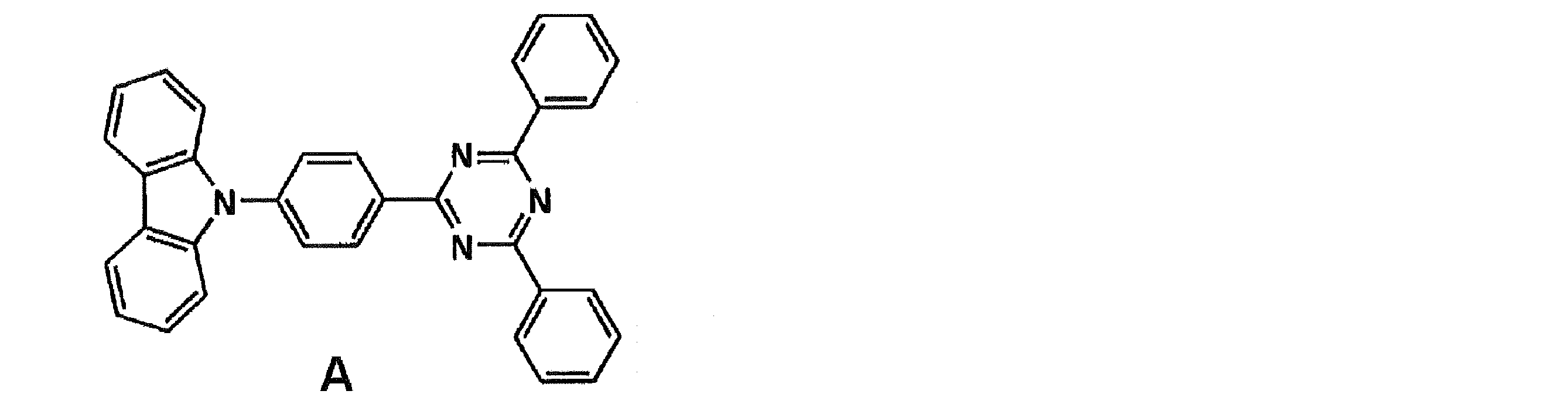
- Patent Document 1 exemplifies Compound A having the following structure, and also describes an example of an organic electroluminescence device using the compound for an electron transport layer. However, no study has been made on compounds in which a substituent is introduced into the carbazolyl group of Compound A. Also, Patent Document 1 does not discuss the usefulness of Compound A as a light emitting material.
- Patent Document 2 describes that a compound having a structure represented by the following general formula emits blue fluorescence, and that the compound is useful as a light emitting device material.
- R 11 and R 12 are a hydrogen atom, an aliphatic hydrocarbon group, an aryl group or a heterocyclic group
- R 1 and R 2 are substituents not containing a hydrogen atom or an amino group
- Patent Document 2 describes that an organic light-emitting device using Compound A as a light-emitting material emits blue fluorescence.
- no study is made on a compound in which a substituent is introduced into the carbazolyl group of Compound A.
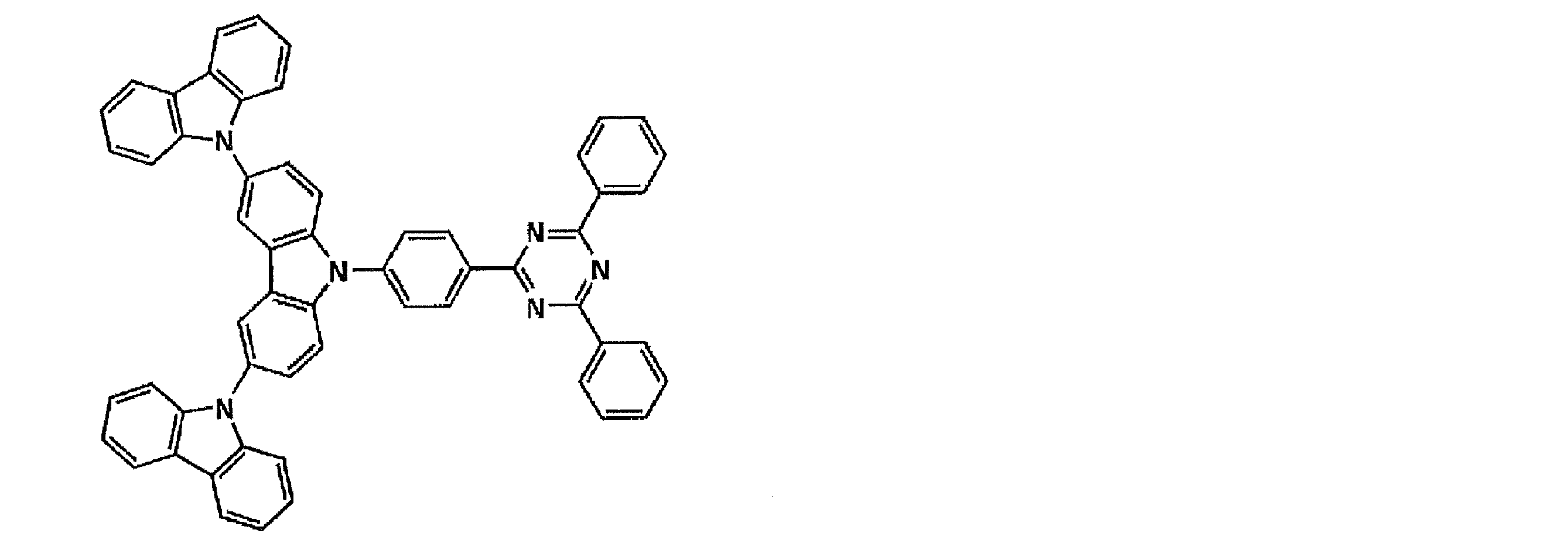
- Patent Document 3 describes a compound having a partial structure in which three carbazole structures are linked, and an example in which a compound having such a partial structure is used as a host material of a light emitting layer of an organic light emitting device is specifically described.
- a compound having such a partial structure is used as a host material of a light emitting layer of an organic light emitting device is specifically described.
- compounds having the following structures are exemplified among many exemplified structures.
- there is no example using the compound and there is no mention of the usefulness of the compound as a light emitting material.
- Patent Document 3 specifically describes the usefulness of Compound A as a luminescent material, but Compound A does not emit delayed fluorescence, and is sufficiently satisfactory in terms of luminous efficiency. is not.
- the present inventors have found that a compound containing a carbazole structure and a 2,4,6-triphenyl-1,3,5-triazine structure is useful as a light emitting material for an organic light emitting device. The study was advanced with the aim of evaluating the details in detail.
- a general formula of a compound that is particularly useful as a light-emitting material has been derived, and intensive studies have been conducted for the purpose of generalizing the structure of an organic light-emitting device having high luminous efficiency.
- the present inventors have obtained a compound containing a carbazole structure and a 2,4,6-triphenyl-1,3,5-triazine structure, It was clarified that a compound satisfying the structural condition is particularly useful as a light emitting material.
- an organic light-emitting device having high emission efficiency has been found by finding that there is a compound useful as a delayed fluorescent material among compounds containing a carbazole structure and a 2,4,6-triphenyl-1,3,5-triazine structure. It was clarified that can be provided at low cost. Based on these findings, the present inventors have provided the following present invention as means for solving the above problems.
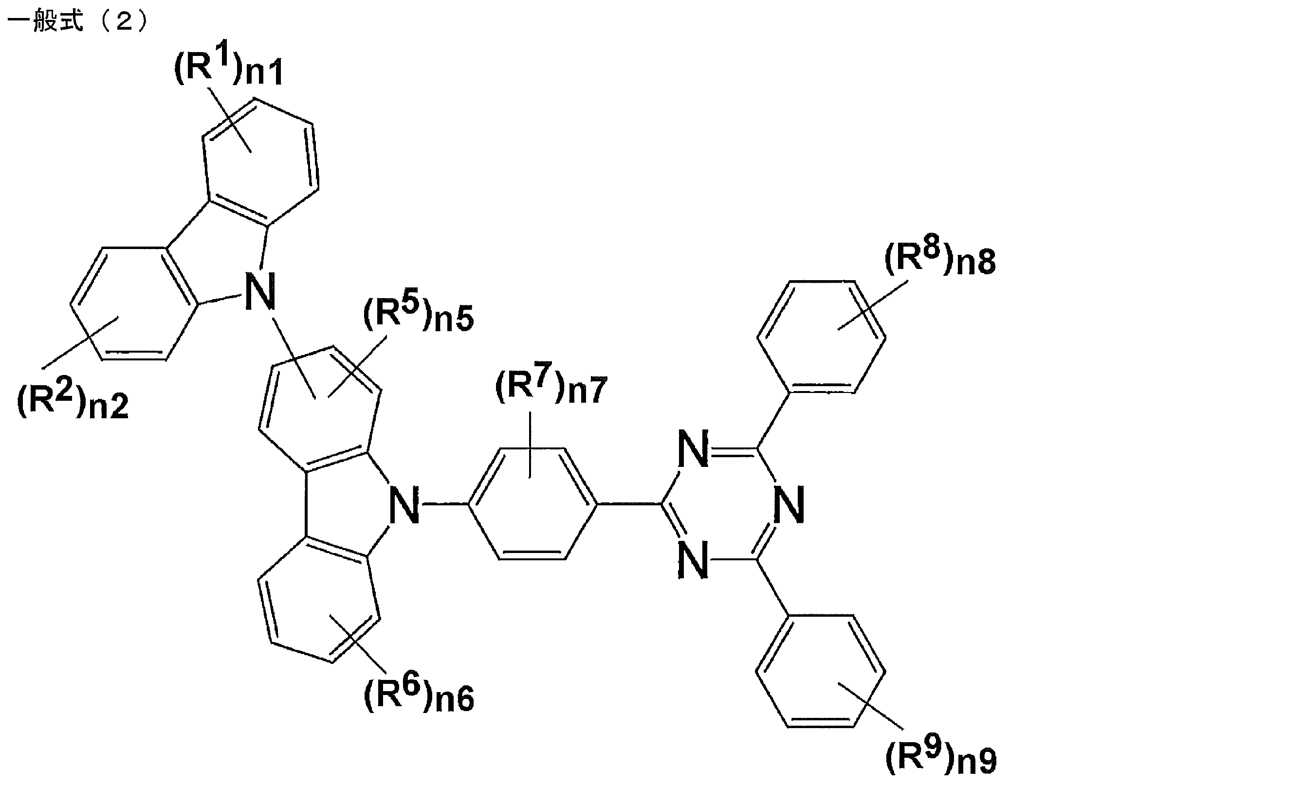
- a light emitting material comprising a compound represented by the following general formula (1).
- R 1 and R 2 are each independently a substituted or unsubstituted carbazolyl group, a substituted or unsubstituted aryl group, a substituted or unsubstituted heteroaryl group, a substituted or unsubstituted alkyl group, Or a substituted or unsubstituted cycloalkyl group
- R 5 and R 6 each independently represents a substituted or unsubstituted alkyl group
- R 7 , R 8 and R 9 each independently represents a substituted or unsubstituted aryl group, a substituted or unsubstituted alkyl group, or a substituted or unsubstituted carbazolyl group
- R 10 represents a carbazolyl group, and the carbazolyl group is a substituted or unsubstituted carbazolyl group, a substituted or unsubstituted
- n1, n2, n6 and n7 each independently represents an integer of 0 to 4
- n5 represents an integer of 0 to 3
- n8 and n9 each independently represents an integer of 0 to 5.
- n10 represents 0 or 1
- a plurality of R 1 , R 2 and R 5 to R 9 corresponding to each of n1, n2 and n5 to n9 are the same or different from each other May be.
- R 1 and R 2 are each independently a substituted or unsubstituted carbazolyl group, a substituted or unsubstituted aryl group, a substituted or unsubstituted heteroaryl group, a substituted or unsubstituted alkyl group, Or a substituted or unsubstituted cycloalkyl group
- R 5 and R 6 each independently represents a substituted or unsubstituted alkyl group
- R 7 , R 8 and R 9 each independently represents a substituted or unsubstituted aryl group, a substituted or unsubstituted alkyl group, or a substituted or unsubstituted carbazolyl group
- n1, n2, n6 and n7 each independently represents an integer of 0 to 4
- n5 represents an integer of 0 to 3
- n8 and n9 each independently represents an integer of 0 to 5.
- R 1 to R 4 are each independently a substituted or unsubstituted carbazolyl group, a substituted or unsubstituted aryl group, a substituted or unsubstituted heteroaryl group, a substituted or unsubstituted alkyl group, Or a substituted or unsubstituted cycloalkyl group, R 5 and R 6 each independently represents a substituted or unsubstituted alkyl group, R 7 , R 8 and R 9 each independently represents a substituted or unsubstituted aryl group, a substituted or unsubstituted alkyl group, or a substituted or unsubstituted carbazolyl group; n1 to n4 and n7 each independently represents an integer of 0 to 4, n5 and n6 each represents an integer of 0 to 3, n8 and n9 each independently represents an integer of 0 to 5.
- n1 to n9 are integers of 2 or more, a plurality of R 1 to R 9 corresponding to each of n1 to n9 may be the same as or different from each other.
- [4] The luminescent material according to any one of [1] to [3], which emits delayed fluorescence.
- [5] The luminescent material according to [2] or [4], wherein n6 in the general formula (2) is 0.
- [6] The luminescent material according to any one of [2], [4], and [5], wherein n1 in the general formula (2) is an integer of 1 to 4.
- [7] The luminescent material as described in [6], wherein R 1 is bonded to the 3-position of the carbazolyl group in the general formula (2).
- R 1 and R 2 in the general formulas (1) and (2) are each independently substituted or unsubstituted 9-carbazolyl group, substituted or unsubstituted phenyl group, substituted or unsubstituted pyridyl group, carbon number
- R 1 and R 2 in the general formulas (1) and (2) are each independently 9-carbazolyl group, phenyl group, tolyl group, dimethylphenyl group, trimethylphenyl group, biphenyl group, pyridyl group, pyrrolyl group, [1]
- R 1 to R 4 in the general formula (3) are each independently substituted or unsubstituted 9-carbazolyl group, substituted or unsubstituted phenyl group, substituted or unsubstituted pyridyl group, having 1 to 6 carbon atoms
- R 1 to R 4 in the general formula (3) are each independently 9-carbazolyl group, phenyl group, tolyl group, dimethylphenyl group, trimethylphenyl group, biphenyl group, pyridyl group, pyrrolyl group, tert-butyl group Or [3], [4], [13], or [14], wherein the luminescent material is a cyclohexyl group.
- the luminescent material according to any one of [3], [4], and [13] to [16], wherein both n5 and n6 in the general formula (3) are 0.
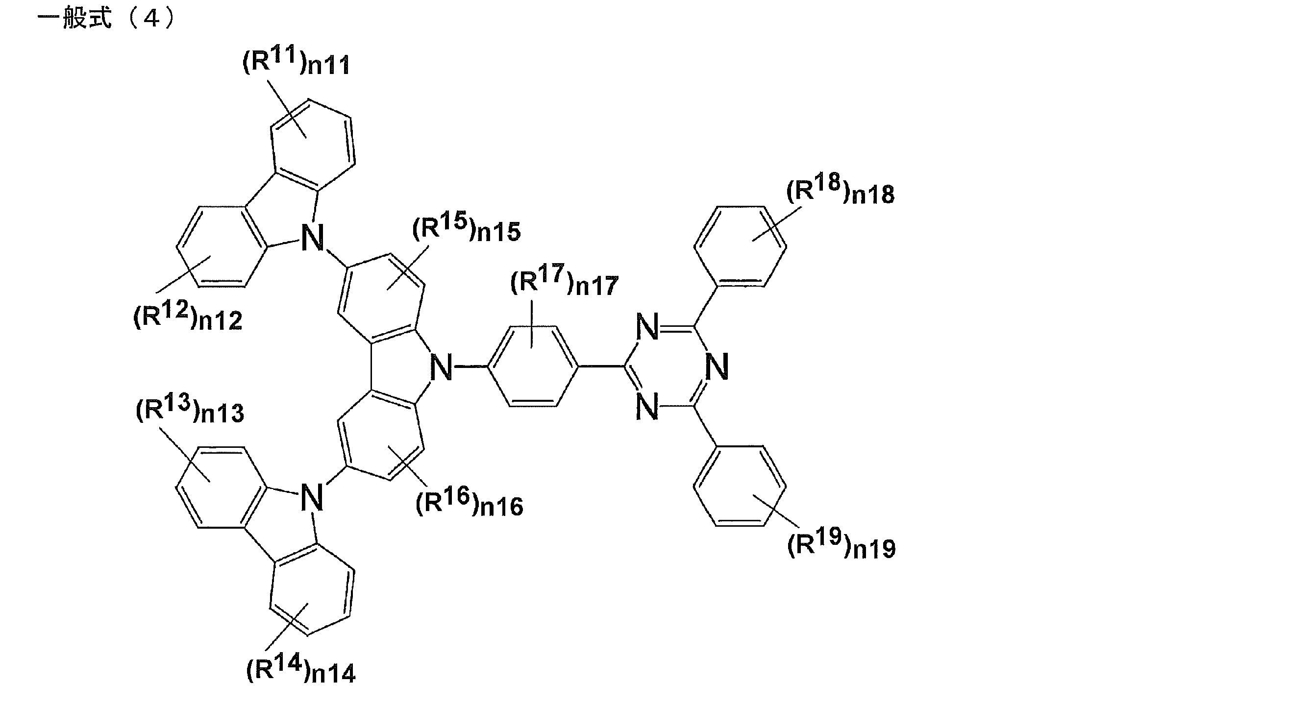
- R 11 to R 14 are each independently a substituted or unsubstituted carbazolyl group, a substituted or unsubstituted aryl group, a substituted or unsubstituted heteroaryl group, a substituted or unsubstituted alkyl group, Or a substituted or unsubstituted cycloalkyl group, R 15 and R 16 each independently represents an alkyl group; R 17 , R 18 and R 19 each independently represent a substituted or unsubstituted aryl group, a substituted or unsubstituted alkyl group, or a substituted or unsubstituted carbazolyl group; n11 to n14 and n17 each independently represents an integer of 0 to 4, n15 and n16 represent any integer of 0 to 3, n18 and n19 each independently represents an integer of 0 to 5.
- n11 to n14 is any integer of 1 to 4.
- n11 to n19 are integers of 2 or more, a plurality of R 11 to R 19 corresponding to each of n11 to n19 may be the same as or different from each other.
- An organic light emitting device comprising a light emitting layer containing the light emitting material according to any one of [1] to [18] on a substrate.
- the organic light-emitting device according to [22] which emits delayed fluorescence.
- the organic light emitting device of the present invention is characterized by high luminous efficiency.
- the compound and the light emitting material of the present invention are effectively used for producing such an organic light emitting device.
- the delayed phosphor of the present invention has a feature that when used as a light emitting layer of an organic light emitting device, the organic light emitting device can emit delayed fluorescence and the luminous efficiency can be dramatically increased.
- 2 is an emission spectrum of an organic photoluminescence element and an organic electroluminescence element using Compound 1.
- 2 is a transient decay curve of an organic electroluminescence device using Compound 1.
- 3 is a graph showing voltage-current density characteristics of an organic electroluminescence device using Compound 1.
- 2 is a graph showing current density-external quantum efficiency characteristics of an organic electroluminescence device using Compound 1.
- 2 is an emission spectrum of an organic photoluminescence device and an organic electroluminescence device using Compound 2.
- 4 is a transient decay curve of an organic electroluminescence device using Compound 2.
- 3 is a graph showing voltage-current density characteristics of an organic electroluminescence device using Compound 2.
- 4 is a graph showing current density-external quantum efficiency characteristics of an organic electroluminescence device using Compound 2.
- 2 is an emission spectrum of an organic photoluminescence device and an organic electroluminescence device using Compound 3.
- 4 is a transient decay curve of an organic electroluminescence device using Compound 3.
- 4 is a graph showing voltage-current density characteristics of an organic electroluminescence device using Compound 3.
- 5 is a graph showing current density-external quantum efficiency characteristics of an organic electroluminescence device using Compound 3.
- 2 is an emission spectrum of an organic photoluminescence device and an organic electroluminescence device using Compound 4.
- FIG. 6 is a graph showing current density-external quantum efficiency characteristics of an organic electroluminescence device using Compound 4.
- 2 is an emission spectrum of an organic photoluminescence device and an organic electroluminescence device using Compound 27.
- 3 is a transient decay curve of an organic electroluminescence device using Compound 27.
- FIG. 3 is a graph showing voltage-current density characteristics of an organic electroluminescence device using Compound 27.
- FIG. 3 is a graph showing current density-external quantum efficiency characteristics of an organic electroluminescence device using Compound 27.
- FIG. 4 is a graph showing voltage-current density characteristics of an organic electroluminescence device using Compound 28. 4 is a graph showing current density-external quantum efficiency characteristics of an organic electroluminescence device using Compound 28.
- 2 is an emission spectrum of an organic photoluminescence device and an organic electroluminescence device using Compound 29. 3 is a transient decay curve of an organic electroluminescence device using Compound 29.
- FIG. 3 is a graph showing voltage-current density characteristics of an organic electroluminescence device using Compound 29.
- FIG. 3 is a graph showing current density-external quantum efficiency characteristics of an organic electroluminescence device using Compound 29.
- a numerical range represented by using “to” means a range including numerical values described before and after “to” as a lower limit value and an upper limit value.
- the isotope species of the hydrogen atom present in the molecule of the compound used in the present invention is not particularly limited. For example, all the hydrogen atoms in the molecule may be 1 H, or a part or all of them are 2 H. (Deuterium D) may be used.
- the luminescent material of the present invention is characterized by comprising a compound represented by the following general formula (1).
- the organic light-emitting device of the present invention is characterized by containing a compound represented by the following general formula (1) as a light-emitting material of the light-emitting layer. Therefore, first, the compound represented by the general formula (1) will be described.
- R 1 and R 2 are each independently a substituted or unsubstituted carbazolyl group, a substituted or unsubstituted aryl group, a substituted or unsubstituted heteroaryl group, a substituted or unsubstituted alkyl group, or Represents a substituted or unsubstituted cycloalkyl group.
- the binding position of the carbazolyl group herein may be any, but is preferably a 9-carbazolyl group or a 3-carbazolyl group, and more preferably a 9-carbazolyl group.
- the aryl group may be a single ring or a fused ring, and preferably has 6 to 14 carbon atoms, more preferably 6 to 10 carbon atoms.
- a preferred specific example is a phenyl group.
- the heteroaryl group may be a single ring or a fused ring, and preferably has 2 to 12 carbon atoms, more preferably 3 to 10 carbon atoms, still more preferably 3 to 6 carbon atoms.
- Specific examples include a pyridyl group and a pyrrolyl group.
- a 1-pyridyl group, a 2-pyridyl group, a 3-pyridyl group, a 1-pyrrolyl group, a 2-pyrrolyl group, and a 3-pyrrolyl group are preferable. It can.
- the alkyl group may be linear or branched, and the carbon number is preferably 1 to 12, more preferably 1 to 6, and still more preferably 1 to 4. Specific examples thereof include a methyl group, an ethyl group, an n-propyl group, an isopropyl group, an n-butyl group, an isobutyl group, and a tert-butyl group, and among them, a tert-butyl group is preferable.
- the cycloalkyl group may be a single ring or a fused ring, and preferably has 5 to 12 carbon atoms, more preferably 5 to 7 carbon atoms. Specific examples include a cyclopentyl group, a cyclohexyl group, and a cycloheptyl group, and among them, a cyclohexyl group can be preferably exemplified.
- the carbazolyl group, aryl group, heteroaryl group, alkyl group and cycloalkyl group that R 1 and R 2 can have may each have a substituent.
- the substitution position and the number of substitutions when having a substituent are not particularly limited.
- the number of substitutions for each group is preferably 0 to 6, more preferably 0 to 4, for example, 0 to 2 is also preferable.
- substituents examples include a hydroxy group, a halogen atom, a cyano group, an alkyl group having 1 to 12 carbon atoms, an alkoxy group having 1 to 12 carbon atoms, an alkylthio group having 1 to 12 carbon atoms, and an alkyl-substituted amino group having 1 to 12 carbon atoms.
- acyl groups having 2 to 12 carbon atoms aryl groups having 6 to 14 carbon atoms, heteroaryl groups having 3 to 13 carbon atoms, diarylamino groups having 12 to 20 carbon atoms, substituted or unsubstituted carbon atoms having 12 to 20 carbon atoms
- Carbazolyl group alkenyl group having 2 to 10 carbon atoms, alkynyl group having 2 to 10 carbon atoms, alkoxycarbonyl group having 2 to 10 carbon atoms, alkylsulfonyl group having 1 to 10 carbon atoms, haloalkyl group having 1 to 10 carbon atoms
- the carbazolyl group, aryl group, heteroaryl group, alkyl group, and cycloalkyl group that can be taken by R 1 and R 2 in the general formula (1) are preferably unsubstituted.
- An alkyl-substituted aryl group is also preferred, and examples thereof include a tolyl group, a dialkylphenyl group, and a trialkylphenyl group. More specifically, a 1-tolyl group, a 2-tolyl group, a 3-tolyl group, 2, Examples include 6-dimethylphenyl group, 2,4-dimethylphenyl group, and 2,4,6-trimethylphenyl group.
- R 1 and R 2 in the general formula (1) are each independently a substituted or unsubstituted 9-carbazolyl group, a substituted or unsubstituted phenyl group, a substituted or unsubstituted pyridyl group, or an alkyl group having 1 to 6 carbon atoms. A cycloalkyl group having 5 to 7 carbon atoms is preferable.
- R 1 and R 2 are each independently a 9-carbazolyl group, phenyl group, tolyl group, dimethylphenyl group, trimethylphenyl group, biphenyl group, pyridyl group, pyrrolyl group, tert-butyl group, or cyclohexyl group. Is more preferable.
- N1 and n2 in the general formula (1) each independently represents an integer of 0 to 4, preferably represents an integer of 0 to 3, and represents an integer of 0 to 2 Is more preferable.
- the plurality of R 1 may be the same or different
- the plurality of R 2 may be the same or different.
- N1 and n2 may be the same or different. When they are the same, for example, the case where all are 0, the case where all are 1, and the case where both are 2 can be exemplified. Moreover, when it differs, the case where n1 is 1 and n2 is 0 can be illustrated.
- R 5 and R 6 each independently represents a substituted or unsubstituted alkyl group.
- R 1 and R 2 can take.
- an unsubstituted alkyl group can be adopted as R 5 and R 6 , or a methyl group can be preferably adopted.
- n5 represents any integer from 0 to 3
- n6 represents any integer from 0 to 4.
- n5 and n6 are preferably each independently 0 to 2, more preferably 0 or 1, and both are preferably 0. In particular, the case where n6 is 0 can be preferably selected.
- n5 is 2 or more
- the plurality of R 5 may be the same or different.
- n6 is 2 or more
- the plurality of R 6 may be the same or different.
- n5 and n6 may be the same or different. When they are the same, for example, when all are 0, a case where both are 1 can be preferably exemplified.
- R 7 , R 8 and R 9 each independently represents a substituted or unsubstituted aryl group, a substituted or unsubstituted alkyl group, or a substituted or unsubstituted carbazolyl group.
- n7 represents any integer of 0 to 4
- n8 and n9 each independently represents any integer of 0 to 5.
- n7 is preferably 0 to 2, more preferably 0 or 1, and also preferably 0.
- n8 and n9 are preferably 0 to 2, and more preferably 0 or 1.
- the plurality of R 7 may be the same or different, and when n8 is 2 or more, the plurality of R 8 may be the same or different.
- n9 2 or more, the plurality of R 9 may be the same or different.
- n8 and n9 may be the same or different. When they are the same, for example, when all are 0, a case where both are 1 can be preferably exemplified. Moreover, when different, the case where n8 is 1 and n9 is 0 can be illustrated.
- R 8 and R 9 in the general formula (1) include a phenyl group, a tolyl group, a dimethylphenyl group, and a trimethylphenyl group. More specifically, a phenyl group, a 1-tolyl group, Examples include 2-tolyl group, 3-tolyl group, 2,6-dimethylphenyl group, 2,4-dimethylphenyl group, and 2,4,6-trimethylphenyl group. It is also preferred that R 8 and R 9 in the general formula (1) are substituted or unsubstituted carbazolyl groups.
- the substituted or unsubstituted carbazolyl group is preferably bonded to the 4-position of the phenyl group bonded to the triazine ring.
- examples of the substituted carbazolyl group mentioned here include a carbazolyl group substituted with a carbazolyl group.
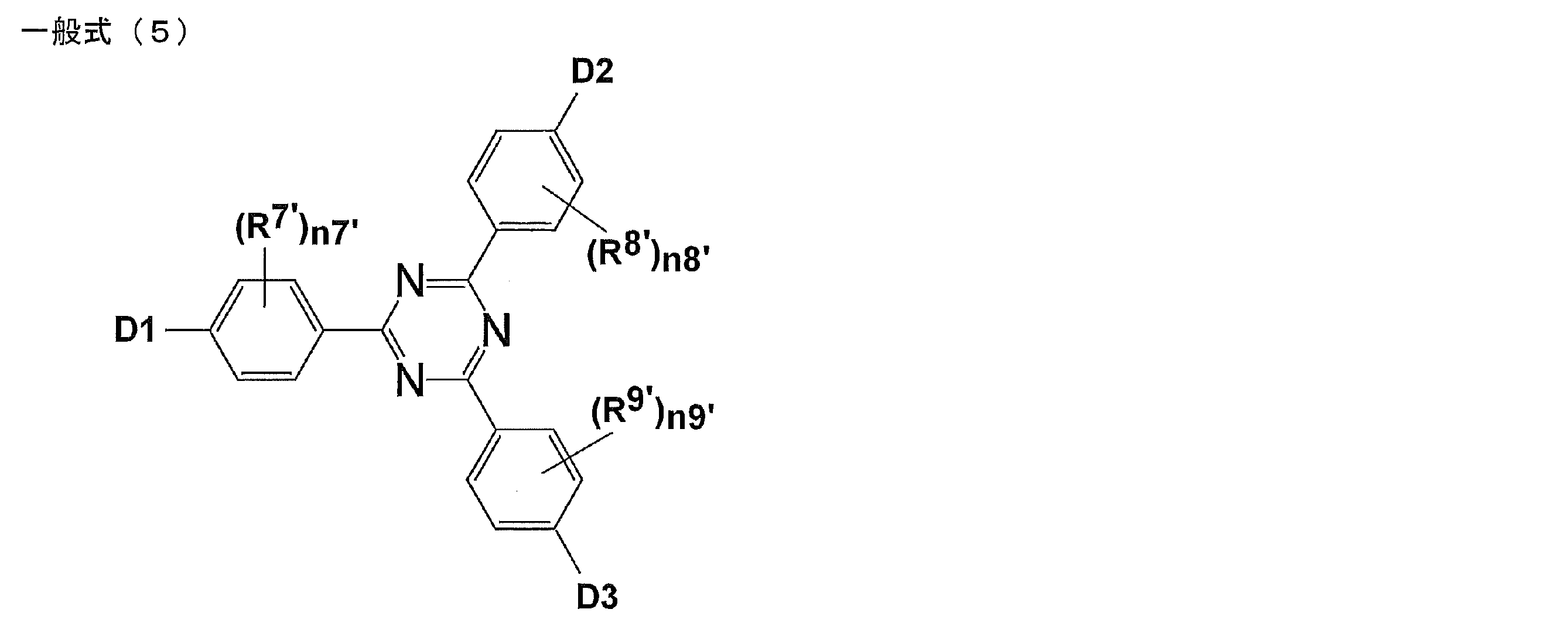
- a structure represented by the following general formula (5) can be preferably exemplified.
- D1 to D3 each independently have a structure represented by the following general formula (6).
- D3 may be a hydrogen atom, a substituted or unsubstituted aryl group, or a substituted or unsubstituted alkyl group.
- R 7 ′ , R 8 ′ and R 9 ′ each independently represents a substituted or unsubstituted aryl group or a substituted or unsubstituted alkyl group.
- n7 ′, n8 ′ and n9 ′ each independently represents an integer of 0 to 4.
- D1 and D2 in the general formula (5) may be the same or different. Further, when D3 has a structure represented by the general formula (6), D1 to D3 may all be the same, or any two may be the same or all may be different. A compound in which all of D1 to D3 are the same has an advantage that it is easy to synthesize.
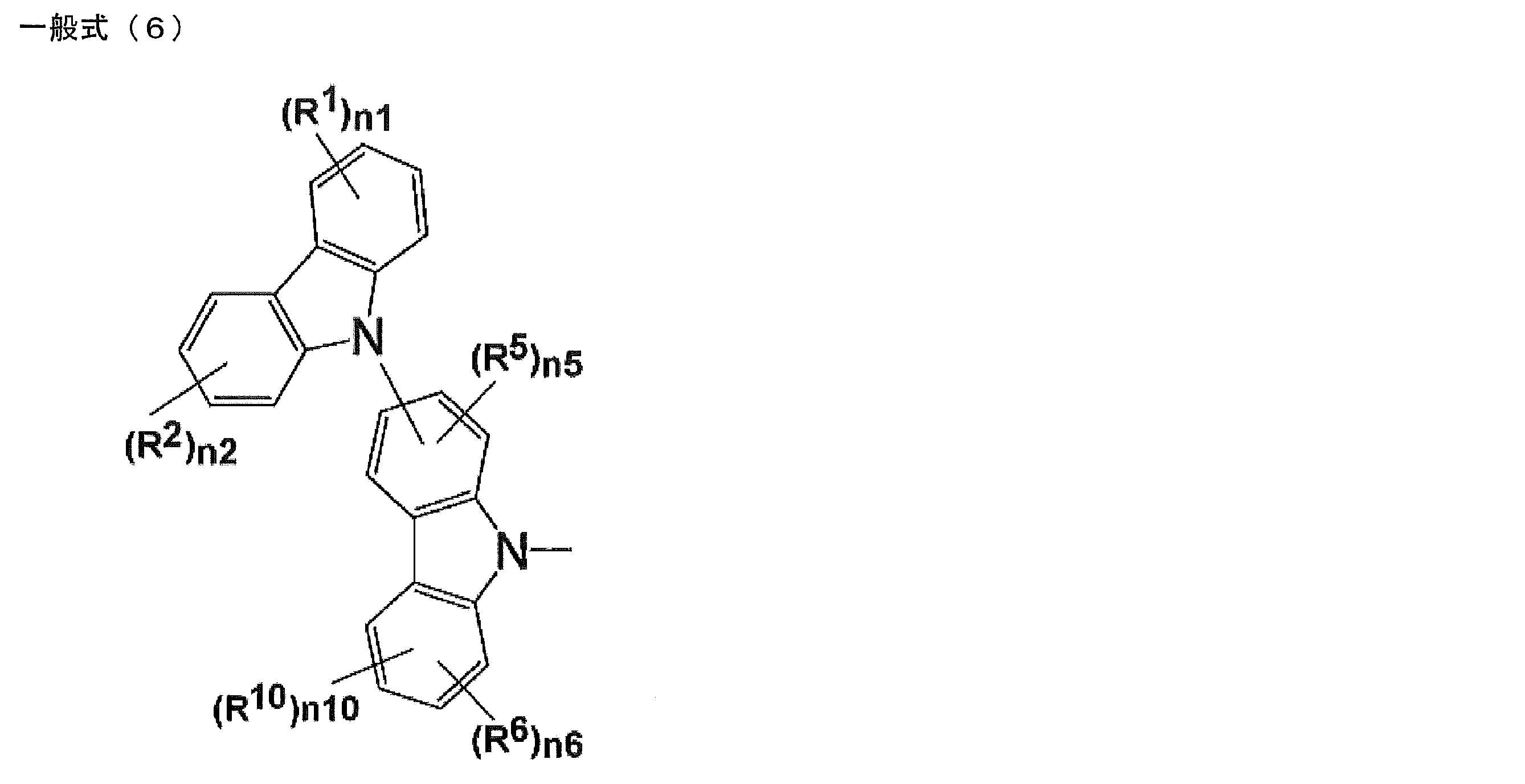
- R 10 in the general formulas (1) and (6) represents a carbazolyl group
- the carbazolyl group is a substituted or unsubstituted carbazolyl group, a substituted or unsubstituted aryl group, a substituted or unsubstituted heteroaryl group, substituted or It may be substituted with an unsubstituted alkyl group or a substituted or unsubstituted cycloalkyl group.
- n10 represents 0 or 1.
- the compound represented by the general formula (1) in which n10 is 0 can be represented by the following general formula (2), and the compound represented by the general formula (1) in which n10 is 1 is represented by the following general formula (3).
- the bonding position may be any one of positions 1 to 8 of the carbazole ring. Preferred is the 2-7 position, more preferred are the 3, 4, 6, 7 positions, and even more preferred are the 3, 6 positions.
- n1 is any integer of 1 to 4 and R 1 is bonded to the 3-position of the carbazole ring
- n2 is any integer of 1 to 4 and carbazo-
- R 2 is bonded to the 6-position of the ring
- n1 and n2 are both integers from 1 to 4
- R 1 is bonded to the 3-position of the carbazole ring and the 6-position.
- bonded can be mentioned preferably.
- R 1 and R 2 when both R 1 and R 2 are present, R 1 and R 2 may be the same or different.
- the substitution position when R 5 is present, the substitution position may be any one of positions 1 to 4 of the carbazole ring that is not substituted with a carbazolyl group. The carbazolyl group is preferably substituted at the 3-position of the carbazole ring.
- the substitution position is preferably the 5, 6, 7 position among the 5 to 8 positions of the carbazole ring, more preferably the 6 or 7 position, and the 6 position. Further preferred.
- the substitution position when R 7 is present may be any position on the benzene ring.
- R 8 or R 9 when R 9 is present, the substitution position may be any of the 2-6 positions.
- R 3 and R 4 are each independently a substituted or unsubstituted carbazolyl group, a substituted or unsubstituted aryl group, a substituted or unsubstituted heteroaryl group, a substituted or unsubstituted alkyl group, or Represents a substituted or unsubstituted cycloalkyl group.
- the carbazolyl group, aryl group, heteroaryl group, alkyl group, cycloalkyl group and substituent the corresponding descriptions of R 1 and R 2 in the general formula (1) can be referred to.
- N3 and n4 in the general formula (3) each independently represents an integer of 0 to 4, preferably represents an integer of 0 to 3, and represents an integer of 0 to 2 Is more preferable.
- the plurality of R 3 may be the same or different
- the plurality of R 4 may be the same or different.
- n1 to n4 may be the same or different. When they are the same, for example, the case where all are 0, the case where all are 1, and the case where both are 2 can be exemplified.
- at least one of n1 to n4 is preferably an integer of 1 to 4. It is also preferable that n1 to n4 are each independently an integer of 1 to 4.
- the bonding position when at least one of R 1 to R 4 is present, the bonding position may be any of the 1 to 8 positions of the carbazole ring. Preferred is the 2-7 position, more preferred are the 3, 4, 6, 7 positions, and even more preferred are the 3, 6 positions.
- the 3-position or when the R 1 is attached the 3-position when R 2 is bonded to R 1 are bonded to 6-position, 3-position when R 1 and R 3 are bonded
- R 1 and R 3 are bonded to the 3- position and R 2 and R 4 are bonded to the 6-position.
- two or more R 1 to R 4 when two or more R 1 to R 4 are present, they may be the same or different.
- the substitution position when R 5 is present, the substitution position may be any one of positions 1 to 4 of the carbazole ring that is not substituted with a carbazolyl group.
- the substitution position when R 6 is present, the substitution position may be any position as long as it is not substituted with the carbazolyl group among the 5 to 8 positions of the carbazole ring.
- the carbazolyl group is preferably substituted at the 3-position and 6-position of the carbazole ring.
- the substitution position when R 7 is present may be any position on the benzene ring. Further, when R 8 or R 9 is present, the substitution position may be any of the 2-6 positions.
- the molecular weight of the compound represented by the general formula (1) is, for example, 1500 or less when the organic layer containing the compound represented by the general formula (1) is intended to be formed by vapor deposition. Preferably, it is preferably 1200 or less, more preferably 1000 or less, and even more preferably 800 or less.
- the lower limit of the molecular weight is 639 or more in the case of the compound represented by the general formula (2), and 804 or more in the case of the compound represented by the general formula (3).
- the compound represented by the general formula (1) may be formed by a coating method regardless of the molecular weight. If a coating method is used, a film can be formed even with a compound having a relatively large molecular weight.
- a compound containing a plurality of structures represented by the general formula (1) in the molecule for the light emitting layer of the organic light emitting device.
- a polymer obtained by polymerizing a polymerizable monomer having a structure represented by the general formula (1) for a light emitting layer of an organic light emitting device for a light emitting layer of an organic light emitting device.
- a polymerizable functional group in any one of R 1 , R 2 , R 5 to R 10 preferably any one of R 1 , R 2 , R 8 , R 9 , R 10 in the general formula (1)
- a polymer having a repeating unit is obtained by polymerizing the monomer alone or copolymerizing with another monomer, and the polymer is used in the light emitting layer of the organic light emitting device. Conceivable. Alternatively, it is also conceivable that dimers and trimers are obtained by coupling compounds having a structure represented by the general formula (1) and used in the light emitting layer of the organic light emitting device.
- L 1 and L 2 represent a linking group.
- the linking group preferably has 0 to 20 carbon atoms, more preferably 1 to 15 carbon atoms, and still more preferably 2 to 10 carbon atoms. And preferably has a structure represented by - linking group -X 11 -L 11.
- X 11 represents an oxygen atom or a sulfur atom, and is preferably an oxygen atom.
- L 11 represents a linking group, preferably a substituted or unsubstituted alkylene group, or a substituted or unsubstituted arylene group, and a substituted or unsubstituted alkylene group having 1 to 10 carbon atoms, or a substituted or unsubstituted group A phenylene group is more preferable.
- R 101 , R 102 , R 103 and R 104 each independently represent a substituent.
- it is a substituted or unsubstituted alkyl group having 1 to 6 carbon atoms, a substituted or unsubstituted alkoxy group having 1 to 6 carbon atoms, or a halogen atom, more preferably an unsubstituted alkyl group having 1 to 3 carbon atoms.
- An unsubstituted alkoxy group having 1 to 3 carbon atoms, a fluorine atom, and a chlorine atom and more preferably an unsubstituted alkyl group having 1 to 3 carbon atoms and an unsubstituted alkoxy group having 1 to 3 carbon atoms.
- any one of R 1 , R 2 , R 5 to R 10 in the general formula (1) preferably any one of R 1 , R 2 , R 8 , R 9 , R 10 are those represented by the following formulas (21) to (24).
- R 1, R 2, 2 or more of R 5 - R 10 is, may be a formula (21) to (24), preferred is the R 1, R 2, R 5 ⁇ R 10 One of them is a case of any one of the following formulas (21) to (24).
- the polymer having a repeating unit containing these formulas (21) to (24) is at least one of R 1 , R 2 and R 5 to R 10 in the general formula (1), preferably R 1 , R 2 , It can be synthesized by making at least one of R 8 , R 9 , and R 10 a hydroxy group, reacting the following compound with it as a linker, introducing a polymerizable group, and polymerizing the polymerizable group. .
- the polymer containing a structure represented by the general formula (1) in the molecule may be a polymer consisting only of a repeating unit having the structure represented by the general formula (1), or other structures may be used. It may be a polymer containing repeating units.
- the repeating unit having a structure represented by the general formula (1) contained in the polymer may be a single type or two or more types. Examples of the repeating unit not having the structure represented by the general formula (1) include those derived from monomers used in ordinary copolymerization. Examples thereof include a repeating unit derived from a monomer having an ethylenically unsaturated bond such as ethylene and styrene.
- the compound represented by the general formula (2) is a novel compound.
- a method for synthesizing the compound represented by the general formula (2) is not particularly limited.
- the compound represented by the general formula (2) can be synthesized by appropriately combining known synthesis methods and conditions. For example, it is possible to synthesize a compound represented by the general formula (2) by the following reaction.
- R 1 , R 2 , R 5 to R 9 and n1, n2, n5 to n9 in the above formula are the same as defined in the general formula (2).
- X represents a halogen atom, preferably a chlorine atom, a bromine atom, or an iodine atom, and more preferably a bromine atom.
- Said reaction can be performed by optimizing suitably the conditions employ
- amines and halides as reaction raw materials can be synthesized by utilizing known synthesis methods. For example, the synthesis method of carbazolylcarbazole can be synthesized with reference to Appl. Phys. Lett. 101, 093306 (2012). The details of the above reaction can be referred to the synthesis examples described below.
- the compound represented by the general formula (2) can also be synthesized by combining other known synthesis reactions.
- R 11 to R 14 are each independently a substituted or unsubstituted carbazolyl group, a substituted or unsubstituted aryl group, a substituted or unsubstituted heteroaryl group, a substituted or unsubstituted alkyl group, or Represents a substituted or unsubstituted cycloalkyl group
- R 15 and R 16 each independently represents an alkyl group
- R 17 , R 18 and R 19 each independently represent a substituted or unsubstituted aryl group, substituted or unsubstituted An alkyl group, or a substituted or unsubstituted carbazolyl group
- n11 to n14 and n17 each independently represents an integer of 0 to 4
- n15 and n16 each represents an integer of 0 to 3
- And n19 each independently represents an integer of 0 to 5.
- n11 to n14 is any integer of 1 to 4.
- n11 to n19 are integers of 2 or more, a plurality of R 11 to R 19 corresponding to each of n11 to n19 may be the same as or different from each other.
- the description of R 1 to R 9 and n1 to n9 in the general formula (1) can be referred to.
- the general formula (4) differs from the n1 to n4 in the general formula (1) in that at least one of n11 to n14 is an integer of any one of 1 to 4.
- at least two of n11 to n14 are more preferably any integer of 1 to 4.
- n11 to n14 are all 1, n11 and n12 are 1, n13 and n14 are 0, n11 and n13 are 1, and n12 and n14 are 0. Can do.
- R 11 to R 14 are present, R 11 and R 13 are preferably bonded to the 3-position of the carbazole ring, and R 12 and R 14 are preferably bonded to the 6-position of the carbazole ring.
- a method for synthesizing the compound represented by the general formula (4) is not particularly limited.
- the synthesis of the compound represented by the general formula (4) can be performed by appropriately combining known synthesis methods and conditions.
- the compound represented by the general formula (4) can be synthesized by the following reaction.
- R 1 to R 9 and n1 to n9 in the above formula are the same as defined in the general formula (3).
- X represents a halogen atom, preferably a chlorine atom, a bromine atom, or an iodine atom, and more preferably a bromine atom.
- Said reaction can be performed by optimizing suitably the conditions employ
- amines and halides as reaction raw materials can be synthesized by utilizing known synthesis methods. For example, the synthesis method of carbazolylcarbazole can be synthesized with reference to Appl. Phys. Lett. 101, 093306 (2012). The details of the above reaction can be referred to the synthesis examples described below.
- the compound represented by General formula (4) is compoundable also by combining another well-known synthetic reaction.
- the compound represented by the general formula (1) of the present invention is useful as a light emitting material of an organic light emitting device. For this reason, the compound represented by General formula (1) of this invention can be effectively used as a luminescent material for the light emitting layer of an organic light emitting element.
- the compound represented by the general formula (1) includes a delayed fluorescent material (delayed phosphor) that emits delayed fluorescence. That is, the present invention relates to a delayed phosphor having a structure represented by the general formula (1), an invention using a compound represented by the general formula (1) as a delayed phosphor, and a general formula (1).
- An invention of a method for emitting delayed fluorescence using the represented compound is also provided.
- An organic light emitting device using such a compound as a light emitting material emits delayed fluorescence and has a feature of high luminous efficiency. The principle will be described below by taking an organic electroluminescence element as an example.
- the organic electroluminescence element carriers are injected into the light emitting material from both positive and negative electrodes to generate an excited light emitting material and emit light.
- 25% of the generated excitons are excited to the excited singlet state, and the remaining 75% are excited to the excited triplet state. Therefore, the use efficiency of energy is higher when phosphorescence, which is light emission from an excited triplet state, is used.
- the excited triplet state has a long lifetime, energy saturation occurs due to saturation of the excited state and interaction with excitons in the excited triplet state, and in general, the quantum yield of phosphorescence is often not high.
- delayed fluorescent materials after energy transition to an excited triplet state due to intersystem crossing, etc., are then crossed back to an excited singlet state due to triplet-triplet annihilation or absorption of thermal energy, and emit fluorescence.
- a thermally activated delayed fluorescent material by absorption of thermal energy is particularly useful.
- excitons in the excited singlet state emit fluorescence as usual.
- excitons in the excited triplet state absorb heat generated by the device and cross between the excited singlets to emit fluorescence.
- the light is emitted from the excited singlet, the light is emitted at the same wavelength as the fluorescence, but the light lifetime (luminescence lifetime) generated by the reverse intersystem crossing from the excited triplet state to the excited singlet state is normal. Since the fluorescence becomes longer than the fluorescence and phosphorescence, it is observed as fluorescence delayed from these. This can be defined as delayed fluorescence. If such a heat-activated exciton transfer mechanism is used, the ratio of the compound in an excited singlet state, which normally generated only 25%, is increased to 25% or more by absorbing thermal energy after carrier injection. It can be raised.
- the heat of the device will sufficiently cause intersystem crossing from the excited triplet state to the excited singlet state and emit delayed fluorescence. Efficiency can be improved dramatically.
- the compound represented by the general formula (1) of the present invention as a light-emitting material of a light-emitting layer, excellent organic light-emitting devices such as an organic photoluminescence device (organic PL device) and an organic electroluminescence device (organic EL device) Can be provided.
- the compound represented by the general formula (1) of the present invention may have a function of assisting light emission of another light emitting material included in the light emitting layer as a so-called assist dopant. That is, the compound represented by the general formula (1) of the present invention contained in the light emitting layer includes the lowest excitation singlet energy level of the host material contained in the light emitting layer and the lowest excitation of other light emitting materials contained in the light emitting layer.
- the organic photoluminescence element has a structure in which at least a light emitting layer is formed on a substrate.
- the organic electroluminescence element has a structure in which an organic layer is formed at least between an anode, a cathode, and an anode and a cathode.
- the organic layer includes at least a light emitting layer, and may consist of only the light emitting layer, or may have one or more organic layers in addition to the light emitting layer. Examples of such other organic layers include a hole transport layer, a hole injection layer, an electron blocking layer, a hole blocking layer, an electron injection layer, an electron transport layer, and an exciton blocking layer.
- the hole transport layer may be a hole injection / transport layer having a hole injection function
- the electron transport layer may be an electron injection / transport layer having an electron injection function.
- FIG. 1 A specific example of the structure of an organic electroluminescence element is shown in FIG.
- 1 is a substrate
- 2 is an anode
- 3 is a hole injection layer
- 4 is a hole transport layer
- 5 is a light emitting layer
- 6 is an electron transport layer
- 7 is a cathode.
- each member and each layer of an organic electroluminescent element are demonstrated.
- substrate and a light emitting layer corresponds also to the board
- the organic electroluminescence device of the present invention is preferably supported on a substrate.
- the substrate is not particularly limited and may be any substrate conventionally used for organic electroluminescence elements.
- a substrate made of glass, transparent plastic, quartz, silicon, or the like can be used.
- an electrode material made of a metal, an alloy, an electrically conductive compound, or a mixture thereof having a high work function (4 eV or more) is preferably used.
- electrode materials include metals such as Au, and conductive transparent materials such as CuI, indium tin oxide (ITO), SnO 2 , and ZnO.
- conductive transparent materials such as CuI, indium tin oxide (ITO), SnO 2 , and ZnO.
- an amorphous material such as IDIXO (In 2 O 3 —ZnO) that can form a transparent conductive film may be used.
- a thin film may be formed by vapor deposition or sputtering of these electrode materials, and a pattern of a desired shape may be formed by photolithography, or when pattern accuracy is not so high (about 100 ⁇ m or more) ), A pattern may be formed through a mask having a desired shape at the time of vapor deposition or sputtering of the electrode material.
- wet film-forming methods such as a printing system and a coating system, can also be used.
- the transmittance be greater than 10%, and the sheet resistance as the anode is preferably several hundred ⁇ / ⁇ or less.
- the film thickness depends on the material, it is usually selected in the range of 10 to 1000 nm, preferably 10 to 200 nm.
- cathode a material having a low work function (4 eV or less) metal (referred to as an electron injecting metal), an alloy, an electrically conductive compound, and a mixture thereof as an electrode material is used.
- electrode materials include sodium, sodium-potassium alloy, magnesium, lithium, magnesium / copper mixture, magnesium / silver mixture, magnesium / aluminum mixture, magnesium / indium mixture, aluminum / aluminum oxide (Al 2 O 3 ) Mixtures, indium, lithium / aluminum mixtures, rare earth metals and the like.
- a mixture of an electron injecting metal and a second metal which is a stable metal having a larger work function value than this for example, a magnesium / silver mixture
- Suitable are a magnesium / aluminum mixture, a magnesium / indium mixture, an aluminum / aluminum oxide (Al 2 O 3 ) mixture, a lithium / aluminum mixture, aluminum and the like.
- the cathode can be produced by forming a thin film of these electrode materials by a method such as vapor deposition or sputtering.
- the sheet resistance as the cathode is preferably several hundred ⁇ / ⁇ or less, and the film thickness is usually selected in the range of 10 nm to 5 ⁇ m, preferably 50 to 200 nm.
- the emission luminance is advantageously improved.
- a transparent or semi-transparent cathode can be produced. By applying this, an element in which both the anode and the cathode are transparent is used. Can be produced.
- the light emitting layer is a layer that emits light after excitons are generated by recombination of holes and electrons injected from each of the anode and the cathode, and the light emitting material may be used alone for the light emitting layer. , Preferably including a luminescent material and a host material.
- a luminescent material the 1 type (s) or 2 or more types chosen from the compound group of this invention represented by General formula (1) can be used.
- a host material in addition to the light emitting material in the light emitting layer.
- the host material an organic compound having at least one of excited singlet energy and excited triplet energy higher than that of the light emitting material of the present invention can be used.
- singlet excitons and triplet excitons generated in the light emitting material of the present invention can be confined in the molecules of the light emitting material of the present invention, and the light emission efficiency can be sufficiently extracted.
- high luminous efficiency can be obtained, so that host materials that can achieve high luminous efficiency are particularly limited. And can be used in the present invention.
- the organic light emitting device or organic electroluminescent device of the present invention light emission is generated from the light emitting material of the present invention contained in the light emitting layer. This emission includes both fluorescence and delayed fluorescence. However, light emission from the host material may be partly or partly emitted.
- the amount of the compound of the present invention, which is a light emitting material is preferably 0.1% by weight or more, more preferably 1% by weight or more, and 50% or more. It is preferably no greater than wt%, more preferably no greater than 20 wt%, and even more preferably no greater than 10 wt%.
- the host material in the light-emitting layer is preferably an organic compound that has a hole transporting ability and an electron transporting ability, prevents the emission of longer wavelengths, and has a high glass transition temperature.
- the injection layer is a layer provided between the electrode and the organic layer for lowering the driving voltage and improving the luminance of light emission.
- the injection layer can be provided as necessary.
- the blocking layer is a layer that can prevent diffusion of charges (electrons or holes) and / or excitons existing in the light emitting layer to the outside of the light emitting layer.
- the electron blocking layer can be disposed between the light emitting layer and the hole transport layer and blocks electrons from passing through the light emitting layer toward the hole transport layer.
- a hole blocking layer can be disposed between the light emitting layer and the electron transporting layer to prevent holes from passing through the light emitting layer toward the electron transporting layer.
- the blocking layer can also be used to block excitons from diffusing outside the light emitting layer. That is, each of the electron blocking layer and the hole blocking layer can also function as an exciton blocking layer.
- the term “electron blocking layer” or “exciton blocking layer” as used herein is used in the sense of including a layer having the functions of an electron blocking layer and an exciton blocking layer in one layer.
- the hole blocking layer has a function of an electron transport layer in a broad sense.
- the hole blocking layer has a role of blocking holes from reaching the electron transport layer while transporting electrons, thereby improving the recombination probability of electrons and holes in the light emitting layer.
- the material for the hole blocking layer the material for the electron transport layer described later can be used as necessary.
- the electron blocking layer has a function of transporting holes in a broad sense.
- the electron blocking layer has a role to block electrons from reaching the hole transport layer while transporting holes, thereby improving the probability of recombination of electrons and holes in the light emitting layer. .
- the exciton blocking layer is a layer for preventing excitons generated by recombination of holes and electrons in the light emitting layer from diffusing into the charge transport layer. It becomes possible to efficiently confine in the light emitting layer, and the light emission efficiency of the device can be improved.
- the exciton blocking layer can be inserted on either the anode side or the cathode side adjacent to the light emitting layer, or both can be inserted simultaneously.
- the layer when the exciton blocking layer is provided on the anode side, the layer can be inserted adjacent to the light emitting layer between the hole transport layer and the light emitting layer, and when inserted on the cathode side, the light emitting layer and the cathode Between the luminescent layer and the light-emitting layer.
- a hole injection layer, an electron blocking layer, or the like can be provided between the anode and the exciton blocking layer adjacent to the anode side of the light emitting layer, and the excitation adjacent to the cathode and the cathode side of the light emitting layer can be provided.
- an electron injection layer, an electron transport layer, a hole blocking layer, and the like can be provided.
- the blocking layer is disposed, at least one of the excited singlet energy and the excited triplet energy of the material used as the blocking layer is preferably higher than the excited singlet energy and the excited triplet energy of the light emitting material.
- the hole transport layer is made of a hole transport material having a function of transporting holes, and the hole transport layer can be provided as a single layer or a plurality of layers.
- the hole transport material has any one of hole injection or transport and electron barrier properties, and may be either organic or inorganic.
- hole transport materials that can be used include, for example, triazole derivatives, oxadiazole derivatives, imidazole derivatives, carbazole derivatives, indolocarbazole derivatives, polyarylalkane derivatives, pyrazoline derivatives and pyrazolone derivatives, phenylenediamine derivatives, arylamine derivatives, Examples include amino-substituted chalcone derivatives, oxazole derivatives, styrylanthracene derivatives, fluorenone derivatives, hydrazone derivatives, stilbene derivatives, silazane derivatives, aniline copolymers, and conductive polymer oligomers, particularly thiophene oligomers.
- An aromatic tertiary amine compound and an styrylamine compound are preferably used, and an aromatic tertiary amine compound is more preferably used.
- the electron transport layer is made of a material having a function of transporting electrons, and the electron transport layer can be provided as a single layer or a plurality of layers.
- the electron transport material (which may also serve as a hole blocking material) may have a function of transmitting electrons injected from the cathode to the light emitting layer.
- Examples of the electron transport layer that can be used include nitro-substituted fluorene derivatives, diphenylquinone derivatives, thiopyran dioxide oxide derivatives, carbodiimides, fluorenylidenemethane derivatives, anthraquinodimethane and anthrone derivatives, oxadiazole derivatives, and the like.
- a thiadiazole derivative in which the oxygen atom of the oxadiazole ring is substituted with a sulfur atom, and a quinoxaline derivative having a quinoxaline ring known as an electron withdrawing group can also be used as an electron transport material.
- a polymer material in which these materials are introduced into a polymer chain or these materials are used as a polymer main chain can also be used.
- the compound represented by the general formula (1) may be used not only for the light emitting layer but also for layers other than the light emitting layer.
- the compound represented by General formula (1) used for a light emitting layer and the compound represented by General formula (1) used for layers other than a light emitting layer may be same or different.
- the compound represented by the general formula (1) may be used for the injection layer, blocking layer, hole blocking layer, electron blocking layer, exciton blocking layer, hole transporting layer, electron transporting layer, and the like. .
- the method for forming these layers is not particularly limited, and the layer may be formed by either a dry process or a wet process.
- the preferable material which can be used for an organic electroluminescent element is illustrated concretely.
- the material that can be used in the present invention is not limited to the following exemplary compounds.
- R and R 1 to R 10 in the structural formulas of the following exemplary compounds each independently represent a hydrogen atom or a substituent.
- n represents an integer of 3 to 5.
- the organic electroluminescence device produced by the above-described method emits light by applying an electric field between the anode and the cathode of the obtained device. At this time, if the light is emitted by excited singlet energy, light having a wavelength corresponding to the energy level is confirmed as fluorescence emission and delayed fluorescence emission. In addition, in the case of light emission by excited triplet energy, a wavelength corresponding to the energy level is confirmed as phosphorescence. Since normal fluorescence has a shorter fluorescence lifetime than delayed fluorescence, the emission lifetime can be distinguished from fluorescence and delayed fluorescence.
- the excited triplet energy is unstable and is converted into heat and the like, and the lifetime is short and it is immediately deactivated.
- the excited triplet energy of a normal organic compound it can be measured by observing light emission under extremely low temperature conditions.
- the organic electroluminescence element of the present invention can be applied to any of a single element, an element having a structure arranged in an array, and a structure in which an anode and a cathode are arranged in an XY matrix.
- an organic light emitting device with greatly improved light emission efficiency can be obtained by containing the compound represented by the general formula (1) in the light emitting layer.
- the organic light emitting device such as the organic electroluminescence device of the present invention can be further applied to various uses. For example, it is possible to produce an organic electroluminescence display device using the organic electroluminescence element of the present invention. For details, see “Organic EL Display” (Ohm Co., Ltd.) ) Can be referred to.
- the organic electroluminescence device of the present invention can be applied to organic electroluminescence illumination and backlights that are in great demand.
- 3-carbazolylcarbazole (0.25 g, 0.75 mmol), 2-bromo-4,6-diphenyl-1,3,5-triazine (0.29 g, 0.75 mmol), copper iodide (0.021 g, 0.11 mmol), 18-crown-6-ether (0.030 g, 0.11 mmol), potassium carbonate (0.62 g, 4.5 mmol) and dodecylbenzene (2. 0 mL) and heated at 220 ° C. for 2 days under an atmosphere of nitrogen gas.
- Example 1 each toluene solution (concentration: 10 ⁇ 5 mol / L) of compounds 1 to 4 and 27 to 29 was prepared and irradiated with light at 300 K while bubbling nitrogen, and light emission was observed.
- the absorption wavelength, emission wavelength, and quantum yield were as shown in Table 1.
- delayed fluorescence was observed in each toluene solution.
- Example 2 an organic photoluminescence element was produced and its characteristics were evaluated.
- Compound 1 and DPEPO are deposited from different deposition sources on a silicon substrate by vacuum deposition under a vacuum degree of 5.0 ⁇ 10 ⁇ 4 Pa. The film was formed at a thickness of 100 nm at 3 nm / second to obtain an organic photoluminescence device.
- An organic photoluminescence device was produced in the same manner using each of the compounds 2 to 4 and 27 to 29 instead of the compound 1.
- the emission spectrum from the thin film when each organic photoluminescence device produced was irradiated with light of 337 nm with an N 2 laser was characterized at 300K.
- the emission spectrum of the organic photoluminescence device using Compound 1 is shown in FIG. 2, the emission spectrum of the organic photoluminescence device using Compound 2 is shown in FIG. 6, and the emission spectrum of the organic photoluminescence device using Compound 3 is shown.
- FIG. 14 shows an emission spectrum of the organic photoluminescence device shown in FIG.
- the emission spectrum of the organic photoluminescence element using the compound 27 is shown in FIG. 18, the emission spectrum of the organic photoluminescence element using the compound 28 is shown in FIG. 22, and the emission spectrum of the organic photoluminescence element using the compound 29 is shown. Is shown in FIG.
- Example 3 an organic electroluminescence element was produced and its characteristics were evaluated. Each thin film was laminated at a vacuum degree of 5.0 ⁇ 10 ⁇ 4 Pa by a vacuum deposition method on a glass substrate on which an anode made of indium tin oxide (ITO) having a thickness of 100 nm was formed. First, ⁇ -NPD was formed on ITO with a thickness of 35 nm, and CBP was formed thereon with a thickness of 10 nm. Further thereon, Compound 1 and DPEPO were deposited from different deposition sources, and a thin film having a concentration of Compound 1 of 6% by weight was formed to a thickness of 15 nm.
- ITO indium tin oxide
- TPBi is formed to a thickness of 40 nm
- further lithium fluoride (LiF) is vacuum-deposited to 0.8 nm
- aluminum (Al) is evaporated to a thickness of 80 nm to form a cathode.
- a luminescence element was obtained.
- An organic electroluminescence device was produced in the same manner using each of the compounds 2 to 4 and 27 to 29 instead of the compound 1.
- Each of the produced organic electroluminescence elements was subjected to a semiconductor parameter analyzer (manufactured by Agilent Technologies: E5273A), an optical power meter measuring device (manufactured by Newport: 1930C), an optical spectrometer (manufactured by Ocean Optics: USB2000), and a streak. Measurement was performed using a camera (C4334 type manufactured by Hamamatsu Photonics Co., Ltd.).
- the emission spectrum of the organic electroluminescence device using Compound 1 is shown in FIG. 2, the transient decay curve under normal pressure and in vacuum is shown in FIG. 3, the voltage-current density characteristics are shown in FIG. 4, and the current density-external quantum efficiency. The characteristics are shown in FIG.
- the emission spectrum of the organic electroluminescence device using Compound 2 is shown in FIG. 6, the transient decay curve under normal pressure and in vacuum is shown in FIG. 7, the voltage-current density characteristics are shown in FIG. 8, and the current density-external quantum efficiency.
- the characteristics are shown in FIG.
- the emission spectrum of the organic electroluminescence device using Compound 3 is shown in FIG. 10
- the transient decay curve under normal pressure and in vacuum is shown in FIG. 11
- the voltage-current density characteristics are shown in FIG. 12
- the current density-external quantum efficiency The characteristics are shown in FIG.
- the emission spectrum of the organic electroluminescence device using Compound 4 is shown in FIG. 14, the transient decay curve under normal pressure and in vacuum is shown in FIG. 15, the voltage-current density characteristic is shown in FIG.
- FIG. 16 the emission spectrum of the organic electroluminescence device using Compound 27
- FIG. 19 the transient decay curve under normal pressure and in vacuum
- FIG. 20 the voltage-current density characteristic
- FIG. 20 the current density-external
- the quantum efficiency characteristics are shown in FIG.
- the emission spectrum of an organic electroluminescence device using Compound 28 is shown in FIG. 22
- the transient decay curve under normal pressure and in vacuum is shown in FIG. 23
- the voltage-current density characteristics are shown in FIG. 24, and the current density-external quantum efficiency.
- the characteristics are shown in FIG.
- the emission spectrum of the organic electroluminescence device using Compound 29 is shown in FIG.
- the transient decay curve shows the result of measuring the luminescence lifetime obtained by measuring the process in which the emission intensity is deactivated by applying excitation light to the compound.
- the light emission intensity decays in a single exponential manner. This means that if the vertical axis of the graph is semi-log, it will decay linearly.
- the transient decay curve of the delayed phosphor such a linear component (fluorescence) is observed in the early stage of observation, but a component deviating from linearity appears after several ⁇ sec.
- the compound of the present invention was a luminescent material containing a delay component in addition to the fluorescent component.
- Comparative Example 1 a toluene solution (concentration: 10 ⁇ 5 mol / L) of the following compound A described in JP-A-2009-21336 and JP-A-2002-193952 was prepared, and 300 K while bubbling nitrogen. The light emission spectrum shown in FIG. 30 was obtained. Further, the transient decay curve of this solution is as shown in FIG. 31, and no delayed fluorescence component was observed.
- the organic light emitting device of the present invention can realize high luminous efficiency.
- the compound represented by the general formula (1) is useful as a light emitting material for such an organic light emitting device. For this reason, this invention has high industrial applicability.
Abstract
Description


本発明者らはこのような課題を考慮して、カルバゾール構造と2,4,6-トリフェニル-1,3,5-トリアジン構造を含む化合物について、その有機発光素子の発光材料としての有用性を詳細に評価することを目的として検討を進めた。また、発光材料として特に有用な化合物の一般式を導きだし、発光効率が高い有機発光素子の構成を一般化することも目的として鋭意検討を進めた。

R5およびR6は各々独立に置換もしくは無置換のアルキル基を表し、
R7、R8およびR9は各々独立に置換もしくは無置換のアリール基、置換もしくは無置換のアルキル基、または置換もしくは無置換のカルバゾリル基を表し、
R10はカルバゾリル基を表し、該カルバゾリル基は、置換もしくは無置換のカルバゾリル基、置換もしくは無置換のアリール基、置換もしくは無置換のヘテロアリール基、置換もしくは無置換のアルキル基、または置換もしくは無置換のシクロアルキル基で置換されていてもよく、
n1、n2、n6およびn7は各々独立に0~4のいずれかの整数を表し、
n5は0~3のいずれかの整数を表し、
n8およびn9は各々独立に0~5のいずれかの整数を表す。
n10は0または1を表し、
n1、n2およびn5~n9が2以上の整数であるとき、各n1、n2およびn5~n9に対応する複数のR1、R2およびR5~R9はそれぞれ互いに同一であっても異なっていてもよい。]
[2] 一般式(1)で表される化合物が下記一般式(2)で表される化合物であることを特徴とする[1]に記載の発光材料。

R5およびR6は各々独立に置換もしくは無置換のアルキル基を表し、
R7、R8およびR9は各々独立に置換もしくは無置換のアリール基、置換もしくは無置換のアルキル基、または置換もしくは無置換のカルバゾリル基を表し、
n1、n2、n6およびn7は各々独立に0~4のいずれかの整数を表し、
n5は0~3のいずれかの整数を表し、
n8およびn9は各々独立に0~5のいずれかの整数を表す。
n1、n2、n5~n9が2以上の整数であるとき、各n1、n2、n5~n9に対応する複数のR1、R2、R5~R9はそれぞれ互いに同一であっても異なっていてもよい。]
[3] 一般式(1)で表される化合物が下記一般式(3)で表される化合物であることを特徴とする[1]に記載の発光材料。

R5およびR6は各々独立に置換もしくは無置換のアルキル基を表し、
R7、R8およびR9は各々独立に置換もしくは無置換のアリール基、置換もしくは無置換のアルキル基、または置換もしくは無置換のカルバゾリル基を表し、
n1~n4およびn7は各々独立に0~4のいずれかの整数を表し、
n5およびn6は0~3のいずれかの整数を表し、
n8およびn9は各々独立に0~5のいずれかの整数を表す。
n1~n9が2以上の整数であるとき、各n1~n9に対応する複数のR1~R9はそれぞれ互いに同一であっても異なっていてもよい。]
[4] 遅延蛍光を放射することを特徴とする[1]~[3]のいずれか1項に記載の発光材料。
[5] 一般式(2)におけるn6が0であることを特徴とする[2]または[4]に記載の発光材料。
[6] 一般式(2)におけるn1が1~4のいずれかの整数であることを特徴とする[2]、[4]、[5]のいずれか1項に記載の発光材料。
[7] 一般式(2)におけるカルバゾリル基の3位にR1が結合していることを特徴とする[6]に記載の発光材料。
[8] 一般式(2)におけるn2が1~4のいずれかの整数であることを特徴とする[6]または[7]に記載の発光材料。
[9] 一般式(2)におけるカルバゾリル基の6位にR2が結合していることを特徴とする[8]に記載の発光材料。
[10] 一般式(1)および(2)におけるR1およびR2が各々独立に置換もしくは無置換の9-カルバゾリル基、置換もしくは無置換のフェニル基、置換もしくは無置換のピリジル基、炭素数1~6のアルキル基、炭素数5~7のシクロアルキル基であることを特徴とする[1]、[2]、[4]~[9]のいずれか1項に記載の発光材料。
[11] 一般式(1)および(2)におけるR1およびR2が各々独立に9-カルバゾリル基、フェニル基、トリル基、ジメチルフェニル基、トリメチルフェニル基、ビフェニル基、ピリジル基、ピロリル基、tert-ブチル基、またはシクロヘキシル基であることを特徴とする[1]、[2]、[4]~[9]のいずれか1項に記載の発光材料。
[12] 一般式(2)におけるn1とn2がいずれも0であることを特徴とする[2]、[4]、[5]のいずれか1項に記載の発光材料。
[13] 一般式(3)におけるn1~n4の少なくとも1つが1~4のいずれかの整数であることを特徴とする[3]または[4]に記載の発光材料。
[14] 一般式(3)におけるn1~n4が各々独立に1~4のいずれかの整数であることを特徴とする[3]または[4]に記載の発光材料。
[15] 一般式(3)におけるR1~R4が各々独立に置換もしくは無置換の9-カルバゾリル基、置換もしくは無置換のフェニル基、置換もしくは無置換のピリジル基、炭素数1~6のアルキル基、炭素数5~7のシクロアルキル基であることを特徴とする[3]、[4]、[13]、[14]のいずれか1項に記載の発光材料。
[16] 一般式(3)におけるR1~R4が各々独立に9-カルバゾリル基、フェニル基、トリル基、ジメチルフェニル基、トリメチルフェニル基、ビフェニル基、ピリジル基、ピロリル基、tert-ブチル基、またはシクロヘキシル基であることを特徴とする[3]、[4]、[13]、[14]のいずれか1項に記載の発光材料。
[17] 一般式(3)におけるn5とn6がいずれも0であることを特徴とする[3]、[4]、[13]~[16]のいずれか1項に記載の発光材料。
[18] 一般式(1)~(3)におけるn7、n8およびn9がいずれも0であることを特徴とする[1]~[17]のいずれか1項に記載の発光材料。
[19] 上記一般式(1)で表される構造を有する遅延蛍光体。
[20] 上記一般式(2)で表される化合物。
[21] 下記一般式(4)で表される化合物。

R15およびR16は各々独立にアルキル基を表し、
R17、R18およびR19は各々独立に置換もしくは無置換のアリール基、置換もしくは無置換のアルキル基、または置換もしくは無置換のカルバゾリル基を表し、
n11~n14およびn17は各々独立に0~4のいずれかの整数を表し、
n15およびn16は0~3のいずれかの整数を表し、
n18およびn19は各々独立に0~5のいずれかの整数を表す。
ただし、n11~n14の少なくとも1つは1~4のいずれかの整数である。
n11~n19が2以上の整数であるとき、各n11~n19に対応する複数のR11~R19はそれぞれ互いに同一であっても異なっていてもよい。]
[22] [1]~[18]のいずれか1項に記載の発光材料を含む発光層を基板上に有することを特徴とする有機発光素子。
[23] 遅延蛍光を放射することを特徴とする[22]に記載の有機発光素子。
[24] 有機エレクトロルミネッセンス素子であることを特徴とする[22]または[23]に記載の有機発光素子。
本発明の発光材料は、下記一般式(1)で表される化合物からなることを特徴とする。また、本発明の有機発光素子は、下記一般式(1)で表される化合物を発光層の発光材料として含むことを特徴とする。そこで、一般式(1)で表される化合物について、まず説明する。

ここでいうカルバゾリル基の結合位置はいずれであってもよいが、好ましいのは9-カルバゾリル基、3-カルバゾリル基であり、より好ましいのは9-カルバゾリル基である。
アリール基は、単環であっても融合環であってもよく、炭素数は6~14が好ましく、6~10がより好ましい。好ましい具体例としてフェニル基を挙げることができる。
ヘテロアリール基も、単環でも融合環でもよく、炭素数は2~12が好ましく、3~10がより好ましく、3~6がさらに好ましい。具体例としてピリジル基、ピロリル基を挙げることができ、なかでも1-ピリジル基、2-ピリジル基、3-ピリジル基、1-ピロリル基、2-ピロリル基、3-ピロリル基を好ましく挙げることができる。
アルキル基は、直鎖状、分枝状のいずれであってもよく、炭素数は1~12が好ましく、1~6がより好ましく、1~4がさらに好ましい。具体例としてメチル基、エチル基、n-プロピル基、イソプロピル基、n-ブチル基、イソブチル基、tert-ブチル基を挙げることができ、なかでもtert-ブチル基を好ましく挙げることができる。
シクロアルキル基は、単環でも融合環でもよく、炭素数が5~12が好ましく、5~7がより好ましい。具体例としてシクロペンチル基、シクロヘキシル基、シクロヘプチル基を挙げることができ、なかでもシクロヘキシル基を好ましく挙げることができる。
n5は0~3のいずれかの整数を表し、n6は0~4のいずれかの整数を表す。n5およびn6は各々独立に0~2であることが好ましく、0または1であることがより好ましく、いずれも0であることも好ましい。特に、n6は0である場合を好ましく選択することができる。n5が2以上であるとき、複数のR5は同一であっても異なっていてもよく、また、n6が2以上であるとき、複数のR6は同一であっても異なっていてもよい。n5とn6は、同一であってもよいし、異なっていてもよい。同一であるときは、例えばいずれも0である場合、いずれも1である場合を好ましく例示することができる。
n7は0~4のいずれかの整数を表し、n8およびn9は各々独立に0~5のいずれかの整数を表す。n7は0~2であることが好ましく、0または1であることがより好ましく、0であることも好ましい。n8およびn9は0~2であることが好ましく、0または1であることがより好ましい。n7が2以上であるとき、複数のR7は同一であっても異なっていてもよく、n8が2以上であるとき、複数のR8は同一であっても異なっていてもよく、さらに、n9が2以上であるとき、複数のR9は同一であっても異なっていてもよい。n8とn9は、同一であってもよいし、異なっていてもよい。同一であるときは、例えばいずれも0である場合、いずれも1である場合を好ましく例示することができる。また、異なる場合は、n8が1であってn9が0である場合を例示することができる。
一般式(1)、(6)におけるR10はカルバゾリル基を表し、該カルバゾリル基は、置換もしくは無置換のカルバゾリル基、置換もしくは無置換のアリール基、置換もしくは無置換のヘテロアリール基、置換もしくは無置換のアルキル基、または置換もしくは無置換のシクロアルキル基で置換されていてもよい。カルバゾリル基、アリール基、ヘテロアリール基、アルキル基、シクロアルキル基、置換基の説明と好ましい範囲は、R1およびR2の対応する説明を参照することができる。
n10は0または1を表す。n10が0である一般式(1)で表される化合物は下記一般式(2)で表すことができ、n10が1である一般式(1)で表される化合物は下記一般式(3)で表すことができる。
一般式(2)においてR5が存在する場合の置換位置は、カルバゾール環の1~4位のうちカルバゾリル基で置換されてない位置であればいずれであってもよい。カルバゾリル基はカルバゾール環の3位に置換していることが好ましい。R6が存在する場合の置換位置は、カルバゾール環の5~8位のうち、5、6、7位であるのが好ましく、6または7位であるのがより好ましく、6位であるのがさらに好ましい。
R7が存在する場合の置換位置は、ベンゼン環のいずれの位置であってもよい。また、R8やR9が存在する場合の置換位置は、2~6位のいずれであってもよい。

n1~n4は、同一であってもよいし、異なっていてもよい。同一であるときは、例えばいずれも0である場合、いずれも1である場合、いずれも2である場合を例示することができる。また、異なる場合は、n1とn3が1であって、n2とn4が0である場合、n1とn2が1であって、n3とn4が0である場合を例示することができる。一般式(3)におけるn1~n4は、少なくとも1つが1~4のいずれかの整数であることが好ましい。また、n1~n4が各々独立に1~4のいずれかの整数であることも好ましい。
一般式(3)においてR5が存在する場合の置換位置は、カルバゾール環の1~4位のうちカルバゾリル基で置換されてない位置であればいずれであってもよい。R6が存在する場合の置換位置は、カルバゾール環の5~8位のうちカルバゾリル基で置換されてない位置であればいずれであってもよい。カルバゾリル基は、カルバゾール環の3位および6位に置換していることが好ましい。
R7が存在する場合の置換位置は、ベンゼン環のいずれの位置であってもよい。また、R8やR9が存在する場合の置換位置は、2~6位のいずれであってもよい。


一般式(1)で表される化合物は、分子量にかかわらず塗布法で成膜してもよい。塗布法を用いれば、分子量が比較的大きな化合物であっても成膜することが可能である。
例えば、一般式(1)で表される構造を有する重合性モノマーを重合させた重合体を、有機発光素子の発光層に用いることが考えられる。具体的には、一般式(1)のR1、R2、R5~R10のいずれか、好ましくはR1、R2、R8、R9、R10のいずれかに重合性官能基を有するモノマーを用意して、これを単独で重合させるか、他のモノマーとともに共重合させることにより、繰り返し単位を有する重合体を得て、その重合体を有機発光素子の発光層に用いることが考えられる。あるいは、一般式(1)で表される構造を有する化合物どうしをカップリングさせることにより、二量体や三量体を得て、それらを有機発光素子の発光層に用いることも考えられる。

一般式(17)および(18)において、R101、R102、R103およびR104は、各々独立に置換基を表す。好ましくは、炭素数1~6の置換もしくは無置換のアルキル基、炭素数1~6の置換もしくは無置換のアルコキシ基、ハロゲン原子であり、より好ましくは炭素数1~3の無置換のアルキル基、炭素数1~3の無置換のアルコキシ基、フッ素原子、塩素原子であり、さらに好ましくは炭素数1~3の無置換のアルキル基、炭素数1~3の無置換のアルコキシ基である。


一般式(1)で表される化合物のうち、一般式(2)で表される化合物は新規化合物である。一般式(2)で表される化合物の合成法は特に制限されない。一般式(2)で表される化合物の合成は、既知の合成法や条件を適宜組み合わせることにより行うことができる。例えば、以下の反応により一般式(2)で表される化合物を合成することが可能である。

一般式(1)で表される化合物のうち、下記一般式(4)で表される化合物は新規化合物である。
一般式(4)で表される化合物の合成法は特に制限されない。一般式(4)で表される化合物の合成は、既知の合成法や条件を適宜組み合わせることにより行うことができる。例えば、以下の反応により一般式(4)で表される化合物を合成することが可能である。

本発明の一般式(1)で表される化合物は、有機発光素子の発光材料として有用である。このため、本発明の一般式(1)で表される化合物は、有機発光素子の発光層に発光材料として効果的に用いることができる。一般式(1)で表される化合物の中には、遅延蛍光を放射する遅延蛍光材料(遅延蛍光体)が含まれている。すなわち本発明は、一般式(1)で表される構造を有する遅延蛍光体の発明と、一般式(1)で表される化合物を遅延蛍光体として使用する発明と、一般式(1)で表される化合物を用いて遅延蛍光を発光させる方法の発明も提供する。そのような化合物を発光材料として用いた有機発光素子は、遅延蛍光を放射し、発光効率が高いという特徴を有する。その原理を、有機エレクトロルミネッセンス素子を例にとって説明すると以下のようになる。
有機フォトルミネッセンス素子は、基板上に少なくとも発光層を形成した構造を有する。また、有機エレクトロルミネッセンス素子は、少なくとも陽極、陰極、および陽極と陰極の間に有機層を形成した構造を有する。有機層は、少なくとも発光層を含むものであり、発光層のみからなるものであってもよいし、発光層の他に1層以上の有機層を有するものであってもよい。そのような他の有機層として、正孔輸送層、正孔注入層、電子阻止層、正孔阻止層、電子注入層、電子輸送層、励起子阻止層などを挙げることができる。正孔輸送層は正孔注入機能を有した正孔注入輸送層でもよく、電子輸送層は電子注入機能を有した電子注入輸送層でもよい。具体的な有機エレクトロルミネッセンス素子の構造例を図1に示す。図1において、1は基板、2は陽極、3は正孔注入層、4は正孔輸送層、5は発光層、6は電子輸送層、7は陰極を表わす。
以下において、有機エレクトロルミネッセンス素子の各部材および各層について説明する。なお、基板と発光層の説明は有機フォトルミネッセンス素子の基板と発光層にも該当する。
本発明の有機エレクトロルミネッセンス素子は、基板に支持されていることが好ましい。この基板については、特に制限はなく、従来から有機エレクトロルミネッセンス素子に慣用されているものであればよく、例えば、ガラス、透明プラスチック、石英、シリコンなどからなるものを用いることができる。
有機エレクトロルミネッセンス素子における陽極としては、仕事関数の大きい(4eV以上)金属、合金、電気伝導性化合物およびこれらの混合物を電極材料とするものが好ましく用いられる。このような電極材料の具体例としてはAu等の金属、CuI、インジウムチンオキシド(ITO)、SnO2、ZnO等の導電性透明材料が挙げられる。また、IDIXO(In2O3-ZnO)等非晶質で透明導電膜を作製可能な材料を用いてもよい。陽極はこれらの電極材料を蒸着やスパッタリング等の方法により、薄膜を形成させ、フォトリソグラフィー法で所望の形状のパターンを形成してもよく、あるいはパターン精度をあまり必要としない場合は(100μm以上程度)、上記電極材料の蒸着やスパッタリング時に所望の形状のマスクを介してパターンを形成してもよい。あるいは、有機導電性化合物のように塗布可能な材料を用いる場合には、印刷方式、コーティング方式等湿式成膜法を用いることもできる。この陽極より発光を取り出す場合には、透過率を10%より大きくすることが望ましく、また陽極としてのシート抵抗は数百Ω/□以下が好ましい。さらに膜厚は材料にもよるが、通常10~1000nm、好ましくは10~200nmの範囲で選ばれる。
一方、陰極としては、仕事関数の小さい(4eV以下)金属(電子注入性金属と称する)、合金、電気伝導性化合物およびこれらの混合物を電極材料とするものが用いられる。このような電極材料の具体例としては、ナトリウム、ナトリウム-カリウム合金、マグネシウム、リチウム、マグネシウム/銅混合物、マグネシウム/銀混合物、マグネシウム/アルミニウム混合物、マグネシウム/インジウム混合物、アルミニウム/酸化アルミニウム(Al2O3)混合物、インジウム、リチウム/アルミニウム混合物、希土類金属等が挙げられる。これらの中で、電子注入性および酸化等に対する耐久性の点から、電子注入性金属とこれより仕事関数の値が大きく安定な金属である第二金属との混合物、例えば、マグネシウム/銀混合物、マグネシウム/アルミニウム混合物、マグネシウム/インジウム混合物、アルミニウム/酸化アルミニウム(Al2O3)混合物、リチウム/アルミニウム混合物、アルミニウム等が好適である。陰極はこれらの電極材料を蒸着やスパッタリング等の方法により薄膜を形成させることにより、作製することができる。また、陰極としてのシート抵抗は数百Ω/□以下が好ましく、膜厚は通常10nm~5μm、好ましくは50~200nmの範囲で選ばれる。なお、発光した光を透過させるため、有機エレクトロルミネッセンス素子の陽極または陰極のいずれか一方が、透明または半透明であれば発光輝度が向上し好都合である。
また、陽極の説明で挙げた導電性透明材料を陰極に用いることで、透明または半透明の陰極を作製することができ、これを応用することで陽極と陰極の両方が透過性を有する素子を作製することができる。
発光層は、陽極および陰極のそれぞれから注入された正孔および電子が再結合することにより励起子が生成した後、発光する層であり、発光材料を単独で発光層に使用しても良いが、好ましくは発光材料とホスト材料を含む。発光材料としては、一般式(1)で表される本発明の化合物群から選ばれる1種または2種以上を用いることができる。本発明の有機エレクトロルミネッセンス素子および有機フォトルミネッセンス素子が高い発光効率を発現するためには、発光材料に生成した一重項励起子および三重項励起子を、発光材料中に閉じ込めることが重要である。従って、発光層中に発光材料に加えてホスト材料を用いることが好ましい。ホスト材料としては、励起一重項エネルギー、励起三重項エネルギーの少なくとも何れか一方が本発明の発光材料よりも高い値を有する有機化合物を用いることができる。その結果、本発明の発光材料に生成した一重項励起子および三重項励起子を、本発明の発光材料の分子中に閉じ込めることが可能となり、その発光効率を十分に引き出すことが可能となる。もっとも、一重項励起子および三重項励起子を十分に閉じ込めることができなくても、高い発光効率を得ることが可能な場合もあるため、高い発光効率を実現しうるホスト材料であれば特に制約なく本発明に用いることができる。本発明の有機発光素子または有機エレクトロルミネッセンス素子において、発光は発光層に含まれる本発明の発光材料から生じる。この発光は蛍光発光および遅延蛍光発光の両方を含む。但し、発光の一部或いは部分的にホスト材料からの発光があってもかまわない。
ホスト材料を用いる場合、発光材料である本発明の化合物が発光層中に含有される量は0.1重量%以上であることが好ましく、1重量%以上であることがより好ましく、また、50重量%以下であることが好ましく、20重量%以下であることがより好ましく、10重量%以下であることがさらに好ましい。
発光層におけるホスト材料としては、正孔輸送能、電子輸送能を有し、かつ発光の長波長化を防ぎ、なおかつ高いガラス転移温度を有する有機化合物であることが好ましい。
注入層とは、駆動電圧低下や発光輝度向上のために電極と有機層間に設けられる層のことで、正孔注入層と電子注入層があり、陽極と発光層または正孔輸送層の間、および陰極と発光層または電子輸送層との間に存在させてもよい。注入層は必要に応じて設けることができる。
阻止層は、発光層中に存在する電荷(電子もしくは正孔)および/または励起子の発光層外への拡散を阻止することができる層である。電子阻止層は、発光層および正孔輸送層の間に配置されることができ、電子が正孔輸送層の方に向かって発光層を通過することを阻止する。同様に、正孔阻止層は発光層および電子輸送層の間に配置されることができ、正孔が電子輸送層の方に向かって発光層を通過することを阻止する。阻止層はまた、励起子が発光層の外側に拡散することを阻止するために用いることができる。すなわち電子阻止層、正孔阻止層はそれぞれ励起子阻止層としての機能も兼ね備えることができる。本明細書でいう電子阻止層または励起子阻止層は、一つの層で電子阻止層および励起子阻止層の機能を有する層を含む意味で使用される。
正孔阻止層とは広い意味では電子輸送層の機能を有する。正孔阻止層は電子を輸送しつつ、正孔が電子輸送層へ到達することを阻止する役割があり、これにより発光層中での電子と正孔の再結合確率を向上させることができる。正孔阻止層の材料としては、後述する電子輸送層の材料を必要に応じて用いることができる。
電子阻止層とは、広い意味では正孔を輸送する機能を有する。電子阻止層は正孔を輸送しつつ、電子が正孔輸送層へ到達することを阻止する役割があり、これにより発光層中での電子と正孔が再結合する確率を向上させることができる。
励起子阻止層とは、発光層内で正孔と電子が再結合することにより生じた励起子が電荷輸送層に拡散することを阻止するための層であり、本層の挿入により励起子を効率的に発光層内に閉じ込めることが可能となり、素子の発光効率を向上させることができる。励起子阻止層は発光層に隣接して陽極側、陰極側のいずれにも挿入することができ、両方同時に挿入することも可能である。すなわち、励起子阻止層を陽極側に有する場合、正孔輸送層と発光層の間に、発光層に隣接して該層を挿入することができ、陰極側に挿入する場合、発光層と陰極との間に、発光層に隣接して該層を挿入することができる。また、陽極と、発光層の陽極側に隣接する励起子阻止層との間には、正孔注入層や電子阻止層などを有することができ、陰極と、発光層の陰極側に隣接する励起子阻止層との間には、電子注入層、電子輸送層、正孔阻止層などを有することができる。阻止層を配置する場合、阻止層として用いる材料の励起一重項エネルギーおよび励起三重項エネルギーの少なくともいずれか一方は、発光材料の励起一重項エネルギーおよび励起三重項エネルギーよりも高いことが好ましい。
正孔輸送層とは正孔を輸送する機能を有する正孔輸送材料からなり、正孔輸送層は単層または複数層設けることができる。
正孔輸送材料としては、正孔の注入または輸送、電子の障壁性のいずれかを有するものであり、有機物、無機物のいずれであってもよい。使用できる公知の正孔輸送材料としては例えば、トリアゾール誘導体、オキサジアゾール誘導体、イミダゾール誘導体、カルバゾール誘導体、インドロカルバゾール誘導体、ポリアリールアルカン誘導体、ピラゾリン誘導体およびピラゾロン誘導体、フェニレンジアミン誘導体、アリールアミン誘導体、アミノ置換カルコン誘導体、オキサゾール誘導体、スチリルアントラセン誘導体、フルオレノン誘導体、ヒドラゾン誘導体、スチルベン誘導体、シラザン誘導体、アニリン系共重合体、また導電性高分子オリゴマー、特にチオフェンオリゴマー等が挙げられるが、ポルフィリン化合物、芳香族第3級アミン化合物およびスチリルアミン化合物を用いることが好ましく、芳香族第3級アミン化合物を用いることがより好ましい。
電子輸送層とは電子を輸送する機能を有する材料からなり、電子輸送層は単層または複数層設けることができる。
電子輸送材料(正孔阻止材料を兼ねる場合もある)としては、陰極より注入された電子を発光層に伝達する機能を有していればよい。使用できる電子輸送層としては例えば、ニトロ置換フルオレン誘導体、ジフェニルキノン誘導体、チオピランジオキシド誘導体、カルボジイミド、フレオレニリデンメタン誘導体、アントラキノジメタンおよびアントロン誘導体、オキサジアゾール誘導体等が挙げられる。さらに、上記オキサジアゾール誘導体において、オキサジアゾール環の酸素原子を硫黄原子に置換したチアジアゾール誘導体、電子吸引基として知られているキノキサリン環を有するキノキサリン誘導体も、電子輸送材料として用いることができる。さらにこれらの材料を高分子鎖に導入した、またはこれらの材料を高分子の主鎖とした高分子材料を用いることもできる。

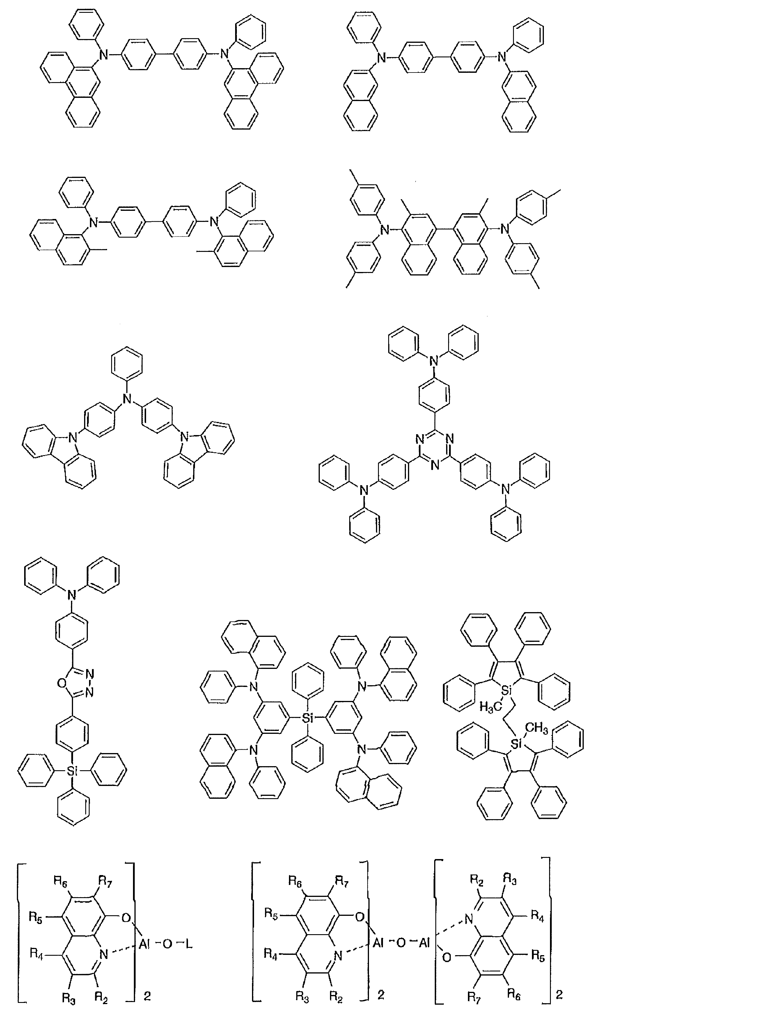
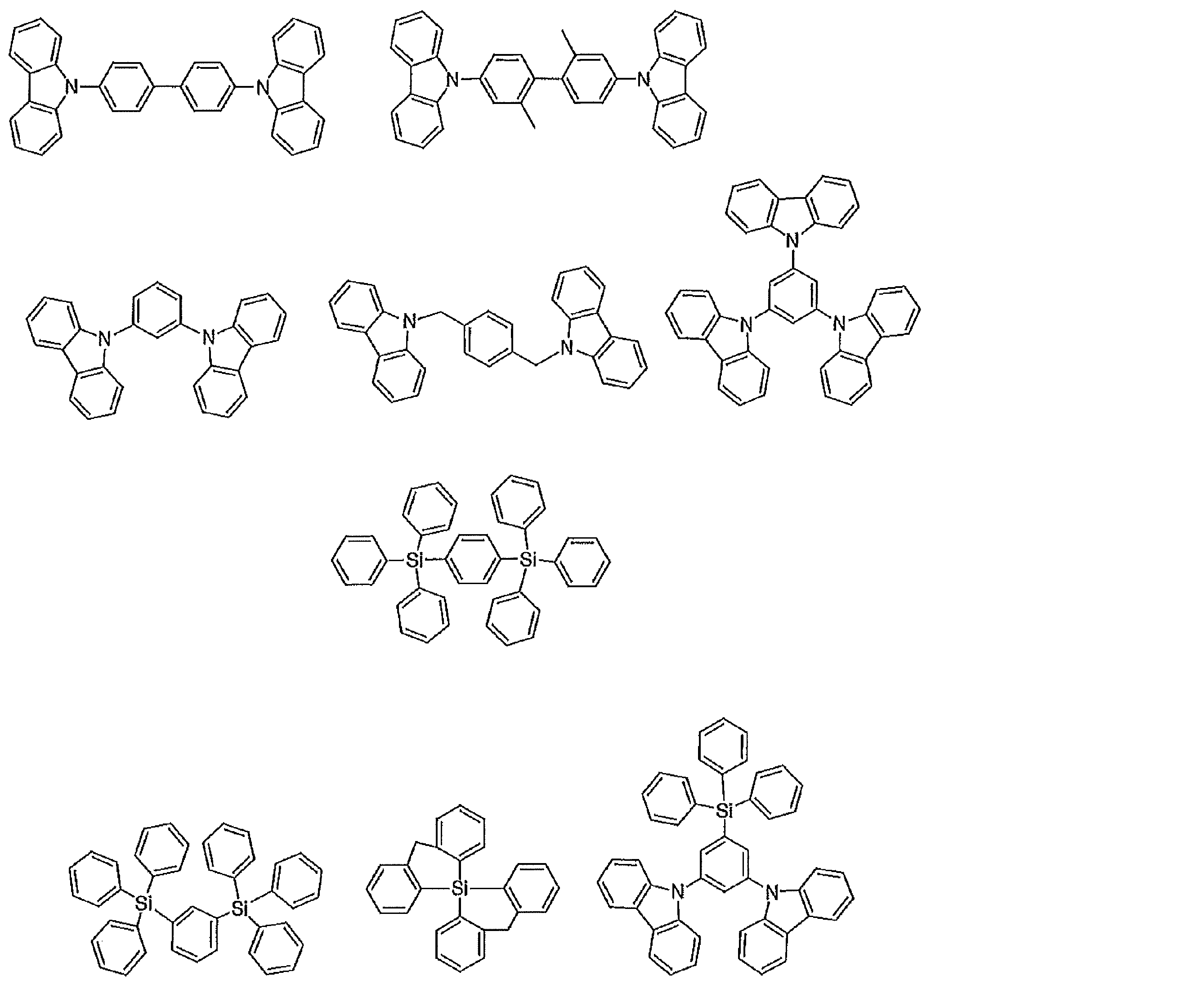
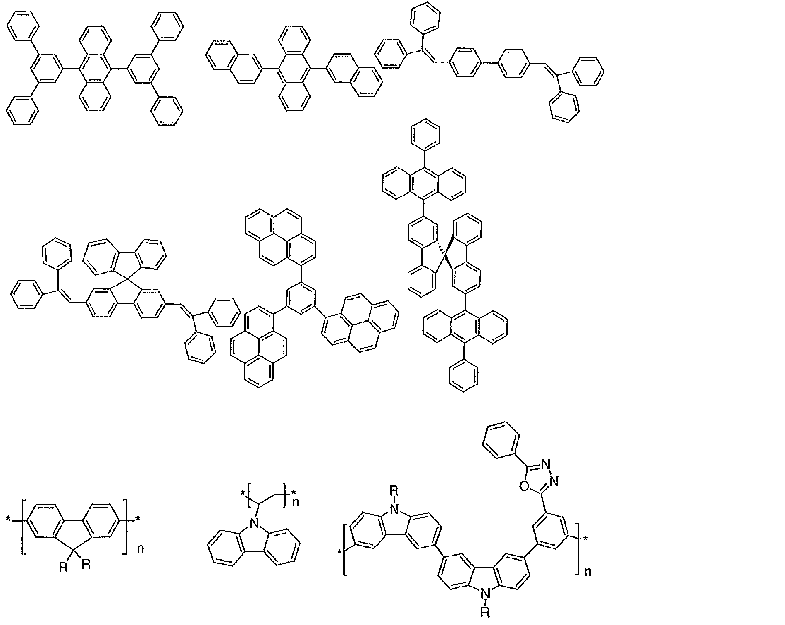
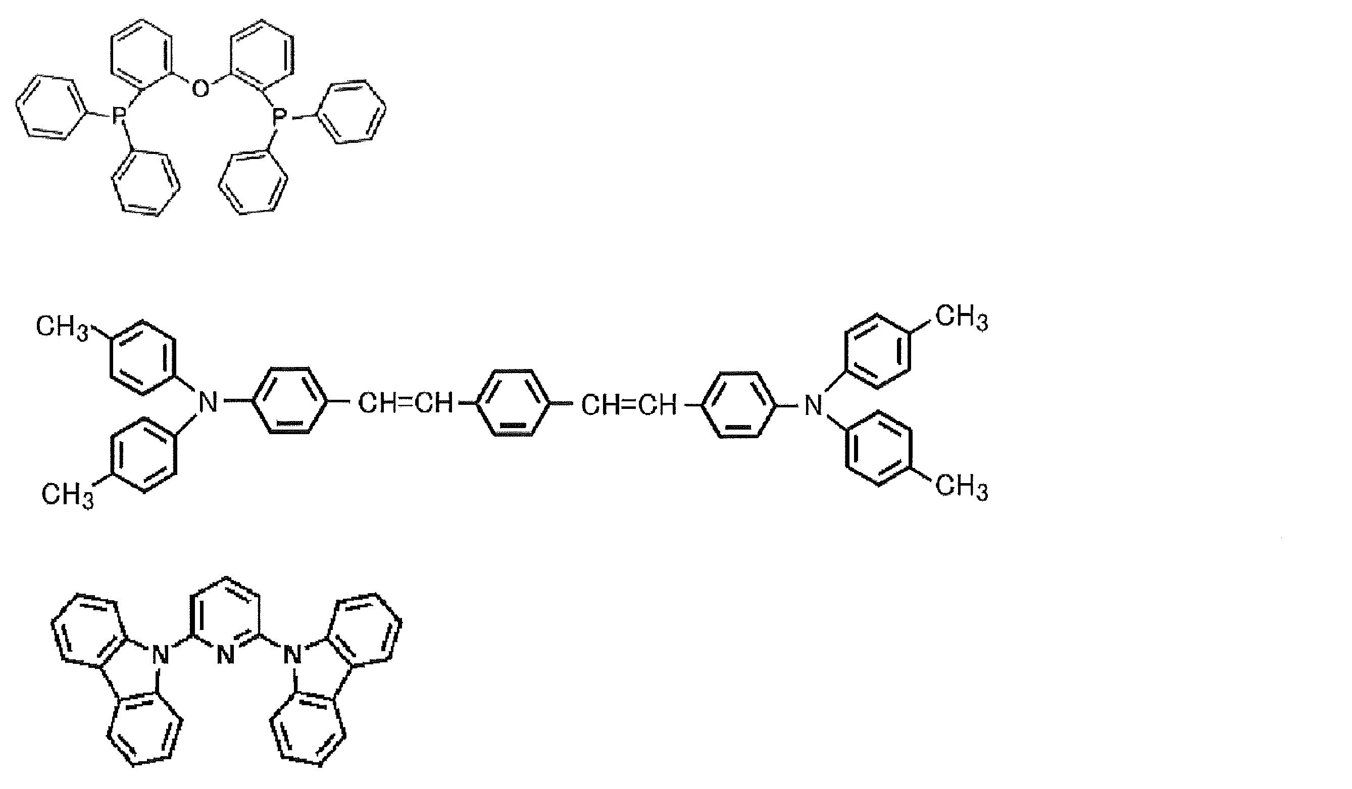

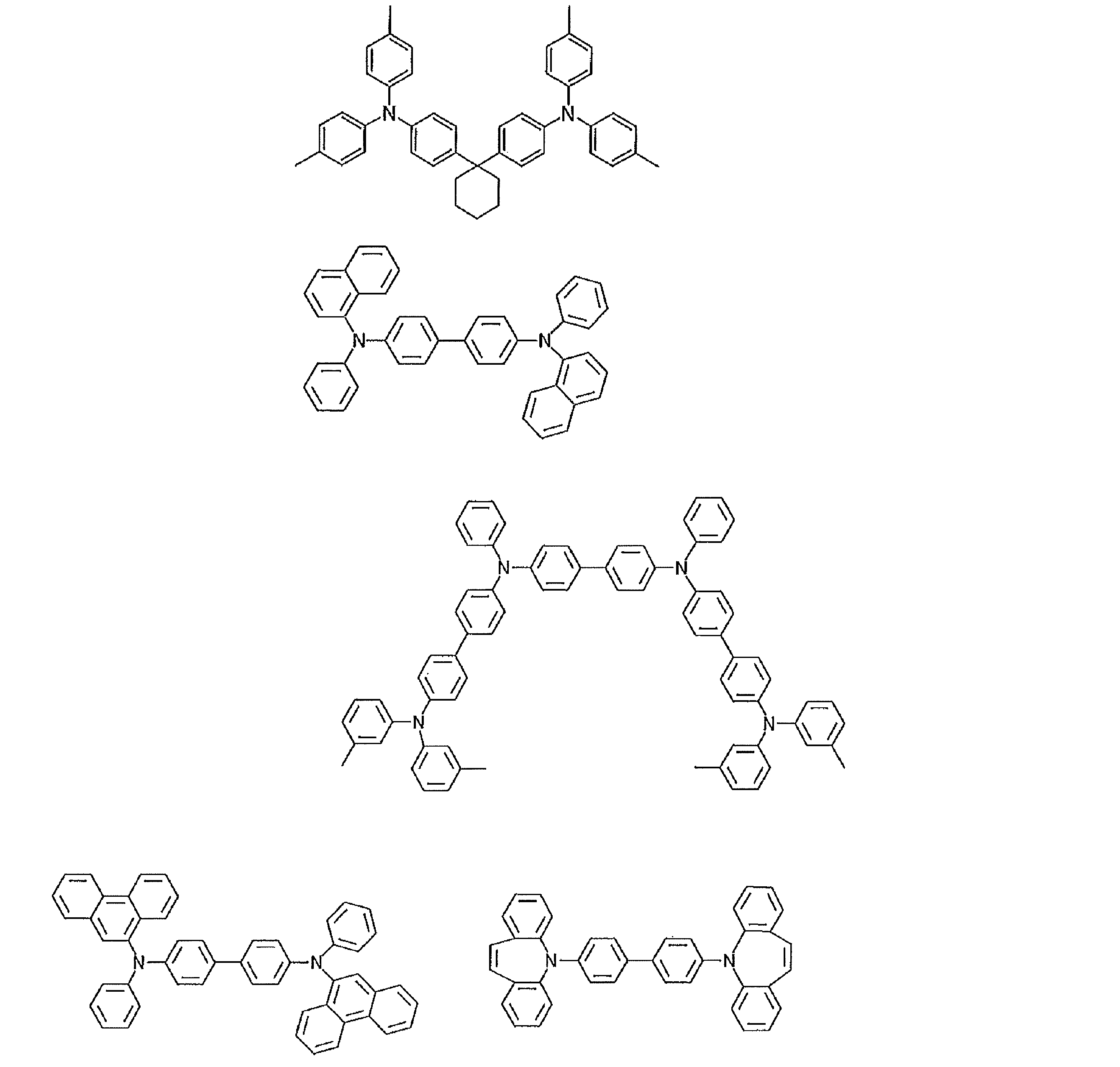
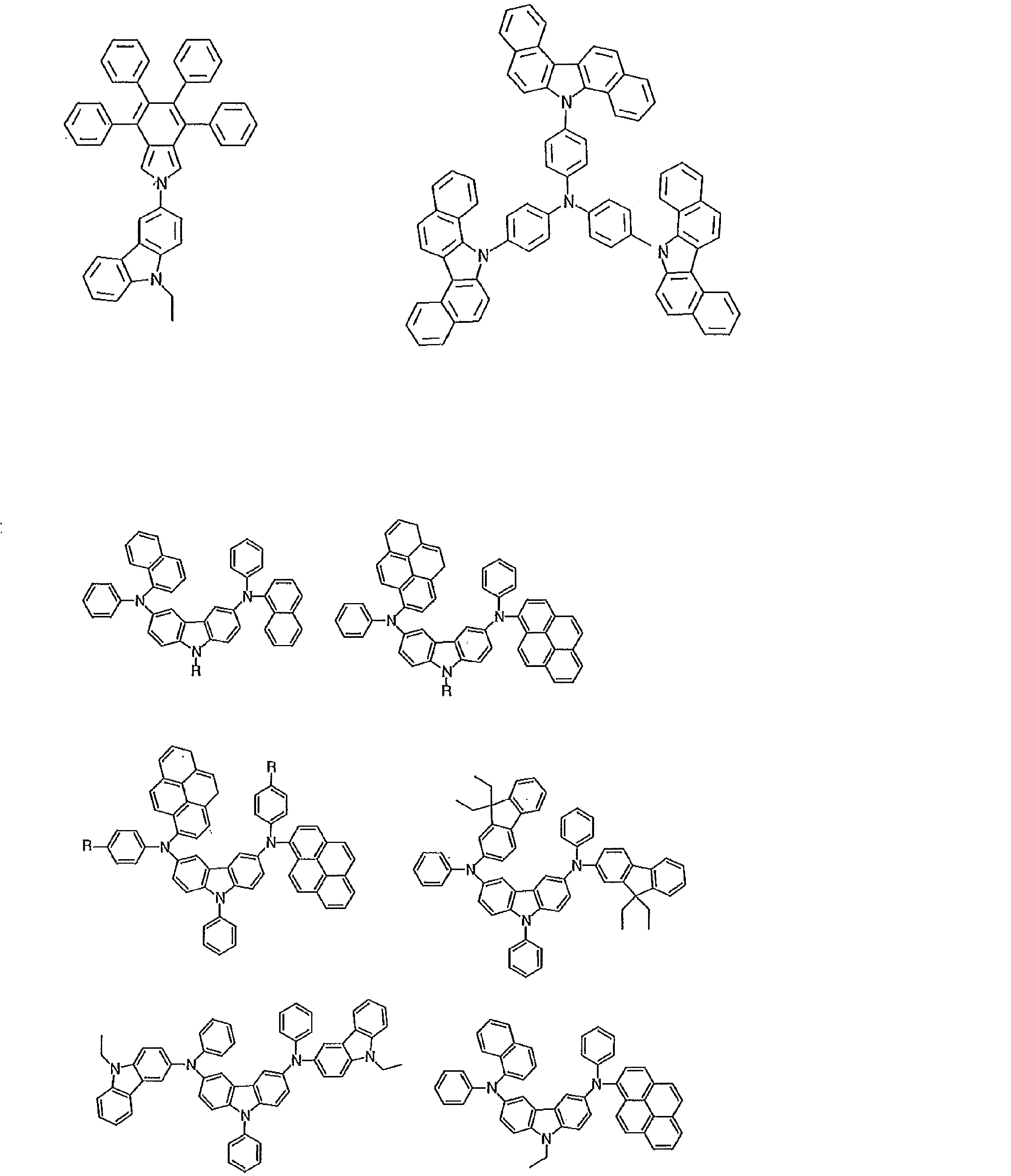


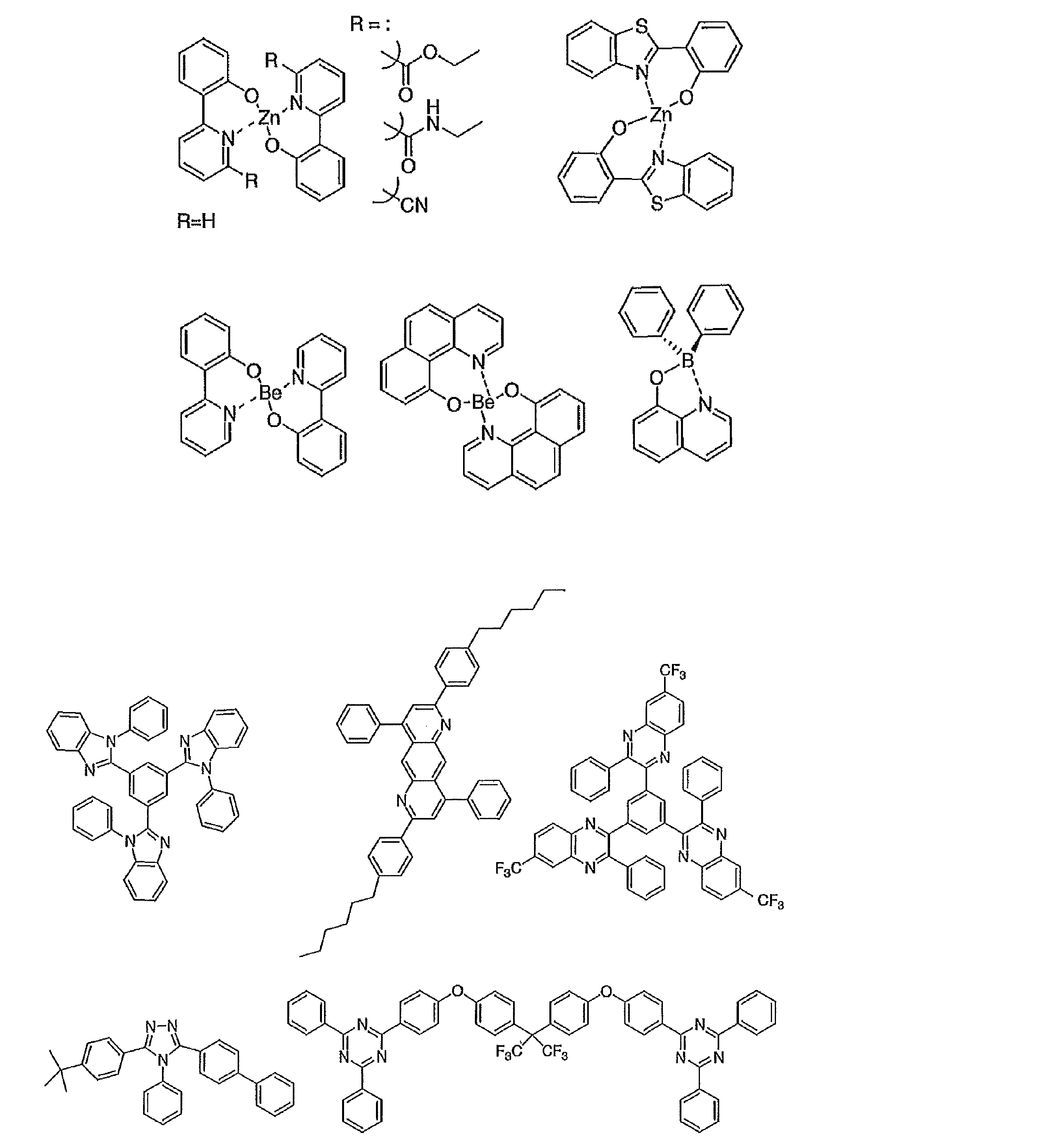


一方、りん光については、本発明の化合物のような通常の有機化合物では、励起三重項エネルギーは不安定で熱等に変換され、寿命が短く直ちに失活するため、室温では殆ど観測できない。通常の有機化合物の励起三重項エネルギーを測定するためには、極低温の条件での発光を観測することにより測定可能である。
本合成例において、以下のスキームにしたがって化合物1を合成した。

1H NMR (500MHz, CDCl3):δ(ppm) 9.08(d, J=9.0Hz, 2H), 8.84(d, J=6.5Hz, 4H), 8.32(d, J=2.0Hz, 1H), 8.20(d, J=8.0Hz, 2H), 8.15(d, J=7.5, 1H), 7.91(d, J=8.5Hz, 2H), 7.75(d, J=9.0Hz, 1H), 7.67-7.59(m, 8H), 7.55-7.51(m, 1H), 7.45-7.41(m, 4H), 7.38-7.35(m, 1H), 7.33-7.29(m, 2H)
本合成例において、以下のスキームにしたがって化合物2を合成した。

3-ブロモ-9-トシル-9H-カルバゾール(4.47g、11.5mmol)、3,6-ジ-tert-ブチル-9H-カルバゾール(3.04g,10.9mmol)、酸化銅(I)(3.96g,27.6mmol)をドデシルベンゼン(2.0mL)に入れ、窒素ガスの環境下、220℃で20時間加熱した。反応終了後、酸化銅(I)をろ過して除去した後、シリカゲルのカラムクロマトグラフィー(展開溶媒:ヘキサン/ジクロロメタン=70/30)にて精製した(収量2.21g(11.5mmol)、収率32.2%)。
1H NMR (500 MHz, CDCl3): δ (ppm) 8.38(d, J=8.5Hz, 1H), 8.16(d, J=1.5Hz, 1H), 8.07(d, J=2.0Hz, 1H), 7.87(d, J=7.5Hz, 1H), 7.80(d, J=8.5Hz, 2H), 7.66(dd, J=2.5Hz,J=2.0Hz, 1H), 7.57-7.53(m, 1H), 7.46(dd, J=2.0Hz, J=1.5Hz, 2H), 7.40-7.37(m, 1H), 7.32(d, J=9.0Hz, 2H), 7.20(d, J=8.0Hz, 2H), 2.33(s, 3H), 1.47(s, 18H)
3,6-ジ-tert-ブチル-9-(9-トシル-9H-カルバゾール-3-イル)-9H-カルバゾール(2.08g,3.47mmol)、水酸化カリウム(2.22g,39.5mmol)をテトラヒドロフラン(4.6mL)とジメチルスルホキシド(2.3mL)と水(0.7mL)の混合溶媒中で70℃で5時間攪拌した。反応終了後、硫酸で中和し、トルエンで抽出後、硫酸ナトリウムで乾燥した。エバポレーターで溶媒を除去した後、再結晶(イソプロパノール/メタノール=50/50)にて精製した(収量1.17g(2.51mmol、収率72.5%)。
1H NMR (500 MHz, DMSO): δ (ppm) 11.54(s, 1H), 8.34(d, J=2.0Hz, 1H), 8.30(d, J=1.5Hz, 2H), 8.20(d, J=8.0Hz, 1H), 7.72(d, J=8.5Hz, 1H), 7.56(d, J=8.5Hz, 1H), 7.53(dd, J=2.0Hz, J=2.0Hz,1H), 7.48-7.44(m, 3H), 7.25(d, J=8.5Hz, 2H), 7.19-7.16(m, 1H), 1.43(s, 18H)
3-(3,6-ジtert-ブチル-カルバゾリル)カルバゾール(0.34g、0.77mmol)、4-ブロモフェニル-ジフェニルトリアジン(0.38g、0.97mmol)にヨウ化銅(0.01g、0.05mmol)、18-クラウン-5-エーテル(0.027g、0.10mmol)、炭酸カリウム(0.138g、1.00mmol)、ドデシルベンゼン(0.9ml)を加え、220℃で一晩反応させた。反応終了後、ジクロロメタンを加えセライトでろ過した。濃縮後、ジクロロメタンで抽出した。有機層を硫酸マグネシウムで乾燥させ、エバポレーターで濃縮した。シリカゲルのカラムクロマトグラフィー(シクロヘキサン/ジクロロメタン=70/30)にて精製することにより化合物2を得た(収量0.3g、粗収率51.9%)。
MALDI-TOF-MS m/z=751([M]+)
1H NMR (500 MHz, DMSO): δ (ppm) 9.08(d, J=8.5Hz, 2H), 8.82(d, J=7.5Hz, 4H), 8.57(d, J=2.0Hz, 1H), 8.41(d, J=7.5Hz, 1H), 8.33(d, J=2.0Hz, 2H), 8.08(d, J=8.5Hz, 2H), 7.82(d, 9.0Hz, 1H), 7.76-7.65(m,8H), 7.58-7.55(m, 1H), 7.50(dd, J=1.5Hz, J=1.5Hz, 2H), 7.39-7.36(m, 1H), 7.33(d, 9.0Hz, 2H), 1.43(s, 18H)
本合成例において、以下のスキームにしたがって化合物3を合成した。

3,6-ジブロモカルバゾール(13g、40mmol)、フェニルボロン酸(11.7g、96mmol)、炭酸ナトリウム(21.9g、207mmol)にトルエン(200ml)、エタノール(100ml)、水(53ml)を加え、脱気後かくはんした。さらにPd(PPh3)4(4.61g、3.99mmol)を加え、脱気後80℃で12時間反応させた。反応終了後、ジクロロメタンで抽出した。有機層を硫酸マグネシウムで乾燥させ、エバポレーターで濃縮した。シリカゲルのカラムクロマトグラフィーにて精製した(溶離液:シクロヘキサン/ジクロロメタン=50/50)。ヘキサンで再結晶した(収量4.32g、収率33.8%)。
1H NMR (500 MHz, CDCl3): δ (ppm) 8.34(d, J=1.5Hz, 2H), 8.11(s, 1H), 7.72(dd, J=1.0Hz, J=1.0Hz, 4H), 7.69(dd, J=1.5Hz, J=2.0Hz, 2H), 7.51-7.46(m, 6H), 7.36-7.33(m, 2H)
3-ブロモ-9-トシル-9H-カルバゾール(4.20g,13.2mmol)、3,6-ジフェニル-9H-カルバゾール(4.87g,12.5mmol)、酸化銅(I)(4.54g,31.8mmol)をドデシルベンゼン(12.3mL)に入れ、窒素ガスの環境下で220℃で20時間加熱した。反応終了後、酸化銅(I)をろ過して除去した後、シリカゲルのカラムクロマトグラフィー(展開溶媒:ヘキサン/ジクロロメタン=50/50)にて精製した(収量3.24g(5.07mmol)、収率38.5%)。
1H NMR (500 MHz, CDCl3): δ (ppm) 8.58(d, J=8.5Hz, 1H), 8.43(d, J=1.5Hz, 2H), 8.41(d, J=8.5Hz, 1H), 8.14(d, J=2.0Hz, 1H), 7.92(d, J=7.5Hz, 1H), 7.84 (d, J=8.5Hz, 2H), 7.75-7.72(m, 6H), 7.68(dd, J=1.5Hz, J=2.0Hz, 2H), 7.59-7.56(m, 1H), 7.52-7.45(m, 5H), 7.42-7.39(m, 1H), 7.37-7.35(m, 2H), 2.34(s, 3H)
3,6-ジフェニル-9-トシル-9H-カルバゾール(3.22g,5.03mmol)、水酸化カリウム(3.22g,57.3mmol)をテトラヒドロフラン(6.7mL)とジメチルスルホキシド(3.3mL)と水(1.0mL)の混合溶媒中で70℃で5時間攪拌した。反応終了後、硫酸で中和し、トルエンで抽出後、硫酸ナトリウムで乾燥した。エバポレーターで溶媒を除去した後、再結晶(クロロホルム/ヘキサン=50/50)にて精製した(収量1.20g(2.48mmol)、収率49.2%)。
1H NMR (500 MHz, CDCl3): δ (ppm) 8.44(d, J=2.0Hz, 2H), 8.29(s, 1H), 8.27(s, 1H), 8.08 (d, J=8.0Hz, 1H), 7.75(d, J=7.0Hz, 4H), 7.68(dd, J=1.5Hz, J=1.5Hz, 2H), 7.60 (dd, J=1.5Hz, J=2.0Hz, 1H), 7.50-7.47(m, 8H), 7.37-7.34(m, 2H), 7.30-7.27(m, 1H)
3-(3,6-ジフェニル-カルバゾリル)カルバゾール(0.35g、0.72mmol)、4-ブロモフェニル-ジフェニルトリアジン(0.31g、0.80mmol)にヨウ化銅(0.010g、0.04mmol)、18-クラウン-5-エーテル(0.038g、0.14mmol)、炭酸カリウム(0.10g、0.72g)、ドデシルベンゼン(0.72ml)を加え、220℃で一晩反応させた。反応終了後、ジクロロメタンを加えセライトでろ過した。濃縮後、ジクロロメタンで抽出し、有機層を硫酸マグネシウムで乾燥させ、エバポレーターで濃縮した。シリカゲルのカラムクロマトグラフィー(ヘキサン/ジクロロメタン=70/30)にて精製することにより化合物3を得た(収量0.10g、収率17.5%)。
1H NMR (500 MHz, DMSO): δ (ppm) 9.09(d, J=8.5Hz, 2H), 8.82(d, J=7.0Hz, 4H), 8.78(d, J=1.5Hz, 2H), 8.68(d, J=2.0Hz, 1H), 8.43(d, J=8.0Hz, 1H), 8.09(d, J=8.5Hz, 2H), 7.85(d, 7.5Hz, 5H), 7.81(dd, J=1.5Hz, J=1.5Hz,2H), 7.76-7.67(m, 9H), 7.53-7.49(m, 6H), 7.42-7.35(m, 3H)
MALDI-TOF-MS:m/z=791([M]+)
本合成例において、以下のスキームにしたがって化合物4を合成した。

3-ブロモ-9-トシル-9H-カルバゾール(1.70g,4.36mmol)、3-カルバゾリルカルバゾール(1.52g,4.59mmol)、酸化銅(I)(2.22g,15.5mmol)をドデシルベンゼン(4.3mL)中で、220℃にて20時間不活性雰囲気下で反応させた。反応終了後、ろ過により酸化銅(I)を除去した後、シリカゲルのカラムクロマトグラフィー(展開溶媒:ヘキサン/ジクロロメタン=50/50)にて精製した(収量1.14g(1.75mmol)、収率38.1%)。
1H NMR(500 MHz, CDCl3): 8.60(d, J=9.0Hz,1H), 8.41(d, J=8.5Hz,1H), 8.31(d, J=1.0Hz,1H), 8.20-8.17(m, 3H), 8.14(d, J=8.0Hz,1H), 7.94(d, J=7.5Hz,1H), 7.84(d, J=8.5Hz,2H), 7.75(dd, J=2.0Hz, J=2.0Hz, 1H),7.58-7.54(m, 3H), 7.48-7.40(m, 7H), 7.35-7.29(m, 3H), 7.22(d, J=8.0Hz,2H), 2.34(s, 3H)
9-(9-(9-トシル-9H-カルバゾリル-3-イル)-9H-カルバゾリル-3-イル)-9H-カルバゾール(1.05g,2.16mmol)、水酸化カリウム(1.38g,24.6mmol)をテトラヒドロフラン(2.9mL)とジメチルスルホキシド(1.4mL)と水(0.4mL)の混合溶媒中で70℃で5時間攪拌した。反応終了後、硫酸で中和し、トルエンで抽出後、硫酸ナトリウムで乾燥した。エバポレーターで溶媒を除去した後、再結晶(クロロホルム/ヘキサン=20/80)にて精製した(収量0.62g(1.3mmol)、収率59%)。
1H NMR(500 MHz, DMSO): 11.62(s, 1H), 8.56(d, J=2.0Hz,1H), 8.50(d, J=2.0Hz,1H), 8.37(d, J=7.5Hz, 1H), 8.29(d, J=8.0Hz,2H), 8.25(d, J=8.0Hz,1H), 7.80(d, J=8.5Hz,1H), 7.66(dd, J=2.0Hz, J=2.0Hz, 1H),7.61-7.7.59(m, 3H), 7.50-7.43(m, 4H), 7.41-7.38(m, 3H), 7.32-7.29(m, 3H), 7.22-7.19 (m, 1H)
)フェニル)-9’H-3,9’:3’,9’’-ターシャルカルバゾールの合成
3-(3-(3-カルバゾリル)カルバゾリル)カルバゾール(0.26g、0.5mmol)、3,6-ジブロモ-9-トシルカルバゾール(0.23g、0.6mmol)、ヨウ化銅(0.005g、0.02mmol)、18-クラウン-6-エーテル(0.025g、0.09mmol)、炭酸カリウム(0.09g、0.65mmol)にドデシルベンゼン(0.6ml)を加え、220℃で一晩反応させた。反応終了後、ジクロロメタンを加えセライトでろ過した。濃縮後、有機層を硫酸マグネシウムで乾燥させ、エバポレーターで濃縮した。シリカゲルのカラムクロマトグラフィーで精製(溶離液:ヘキサン/ジクロロメタン=70/30)することにより化合物4を得た(収量0.11g、収率23.1%)。
1H NMR(500 MHz, CDCl3): 9.10(d, J=8.5Hz, 2H), 8.84(d, J=7.0Hz,4H), 8.41(d, J=2.0Hz, 1H), 8.33(d, J=1.5Hz,1H), 8.20-8.15(m, 4H), 7.92(d, J=8.5Hz,2H), 7.80(d, J=8.5Hz,1H), 7.69-7.55(m, 12H), 7.48(s, 2H),7.43(s, 4H), 7.35-7.29 (m, 3H)
MALDI-TOF-MS:m/z=803([M-1]+)
本合成例において、以下のスキームにしたがって化合物28を合成した。

3,6-ジブロモ-9-トシルカルバゾール(1.92g、4.0mmol)、3,6-ジフェニルカルバゾール(2.58g、8.08mmol)、酸化銅(1.39g、9.7mmol)にドデシルベンゼン(3.5ml)を加え、220℃で一晩反応させた。反応終了後、ジクロロメタンで抽出し、有機層を硫酸マグネシウムで乾燥させ、エバポレーターで濃縮した。シリカゲルのカラムクロマトグラフィー(溶離液:ヘキサン/ジクロロメタン=70/30)で精製した(収量1.42g、収率19.0%).
1H NMR (500 MHz, CDCl3): δ (ppm) 8.66(d, J=9.0Hz, 2H), 8.40(d, J=2.0Hz, 4H), 8.18(d, J=2.0Hz, 2H), 7.97 (d, J=8.50Hz, 2H), 7.82(dd, J=2.0Hz, J=2.0Hz, 2H), 7.72 (d, J=7.0Hz, 8H), 7.67(dd, J=2.0Hz, J=2.0Hz, 4H), 7.48-7.46(m, 12H), 7.36-7.33(m, 6H), 2.42(s, 3H)
9-トシル-3,3”,6,6”テトラフェニル-3’,6’-ジカルバゾリルカルバゾール(0.25g、0.25mmol)、水酸化カリウム(0.14g、2.5mmol)にTHF(2.3ml)、DMSO(1.4ml)、水(0.3ml)を加え、4時間加熱還流させた。反応終了後、1N HClで中和した。水、ジクロロメタンで抽出し、有機層を硫酸マグネシウムで乾燥させた。有機層をエバポレーターで濃縮した。ヘキサン、ジクロロメタンで再結晶した(収量0.16g、収率80.0%)。
1H NMR(500 MHz, CDCl3): δ (ppm) 8.52(s,1H), 8.42(d, J=2.0Hz, 4H), 8.30(d, J=2.0Hz, 2H), 7.77(d, J=8.5Hz, 2H), 7.73(d, J=8.0Hz, 8H), 7.70(d, J=2.0Hz, 1H), 7.67(dd, J=2.0Hz, J=1.5Hz, 5H), 7.49-7.46(m, 12H), 7.35-7.33(m, 4H)
3,3”,6,6”テトラフェニル-3’,6’-ジカルバゾリルカルバゾール(0.97g、1.2mmol)、ジフェニルトリアジン(0.47g、1.21mmol)、ヨウ化銅(0.004g、0.02mmol)、18-クラウン-6-エーテル(0.035g、0.13mmol)、炭酸カリウム(0.17g、1.43mmol)にドデシルベンゼン(1.2ml)を加え、220℃で2日間反応させた。反応終了後、ジクロロメタンで抽出し、有機層を硫酸マグネシウムで乾燥させ、エバポレーターで濃縮した。シリカゲルのカラムクロマトグラフィー(溶離液:ヘキサン/ジクロロメタン=70/30)で精製することにより化合物28を得た(収量0.20g、収率15.3%)。
1H NMR(500MHz, d6-DMSO) : δ (ppm) 9.16(d, J=9.0Hz, 2H), 8.87-8.83(m, 6H), 8.77(d, J=8.5Hz, 4H),8.23(d, J=8.5Hz, 2H),7.96(d, J=8.5Hz, 2H),7.86-7.80(m, 16H), 7.76-7.71(m, 4H), 7.55(d, J=8.5Hz, 4H), 7.52-7.49(m, 8H), 7.37-7.34(m, 4H)
本合成例において、以下のスキームにしたがって化合物29を合成した。
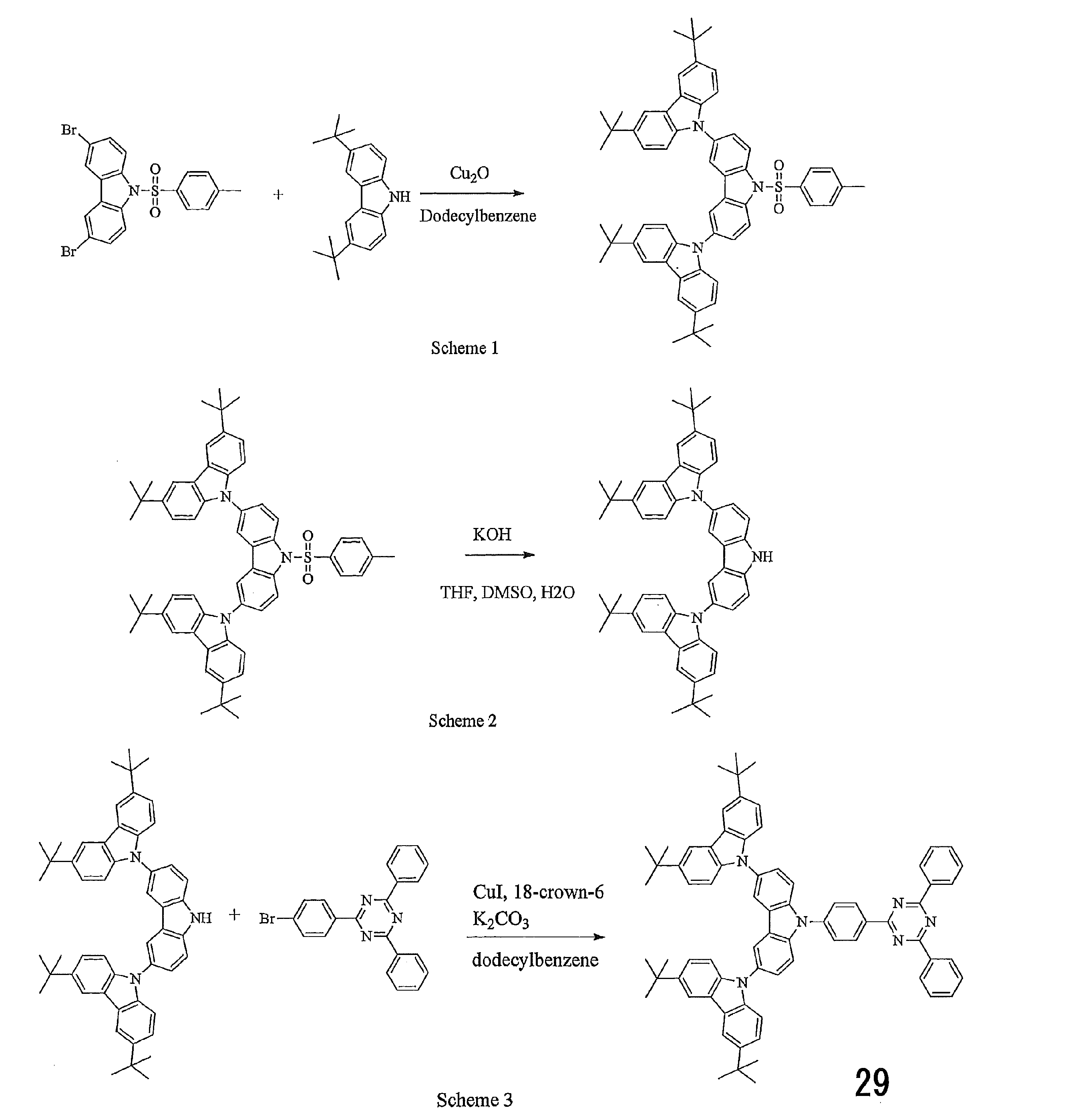
3,6-ジtert-ブチルカルバゾール(2.69g、9.59mmol)、3,6-ジブロモカルバゾール(2.40g、5.00mmol)、酸化銅(1.71g、12.3mmol)にドデシルベンゼン(4ml)、NMP(1ml)を加え、220℃で一晩反応させた。反応終了後、ろ過により酸化銅を取り除き、エバポレーターで濃縮した。シリカゲルのカラムクロマトグラフィー(シクロヘキサン/ジクロロメタン=50/50)により精製したところ、目的物と思われるものが0.44g程度(収率10%程度)であった。さらにモノ体および原料が含まれるものに酸化銅(II)0.85g(5.94mmol)、ドデシルベンゼン(2ml)を加え、220℃で一晩加熱還流させた(収量1.02g、収率23.3%)。
1H NMR(500MHz, CDCl3) :δ(ppm) 8.56(d, J=8.5Hz, 2H), 8.14(d, J=1.5Hz, 4H), 8.05(d, J=2.0Hz, 2H),7.91(d, J=8.5Hz, 2H),7.73(dd, J=2.0Hz, J=2.0Hz, 2H),7.44(dd, J=2.0Hz, J=2.0Hz, 4H), 7.33-7.2.8(m, 6H), 2.39(s, 3H), 1.45(s, 36H)
3,3”,6,6”-テトラ-tert-ブチル-9’-トシル-3’,6’-ジカルバゾリルカルバゾール(4.78g、5.45mmol)、水酸化カリウム(2.41g、56mmol)にTHF(49ml)、DMSO(24ml)、水(5ml)を加えて、3時間加熱かくはんした。反応終了後、1N HClにて中和し、ジクロロメタンで抽出した。有機層を硫酸マグネシウムで乾燥させ、エバポレーターで濃縮した。シリカゲルのカラムクロマトグラフィー(展開溶媒:シクロヘキサン/ジクロロメタン=70/30)で精製した。ヘキサンで再結晶した(収量2.95、収率75%)。
1H NMR(500MHz, CDCl3) :δ(ppm) 8.42(s, 1H), 8.17-8.15(m, 6H), 7.69-7.67(m, 1H), 7.61(d, J=8.5Hz, 2H), 7.65-7.55(m, 1H), 7.47-7.43(m, 4H), 7.32-7.30(m, 4H), 1.48-1.46(m, 36H)
(3,6-ジ(3,6-ジ(tert-ブチルカルバゾリル))-カルバゾール(0.51g、0.7mmol)、3,6-ジブロモ-9-トシルカルバゾール(0.31g、0.81mmol)、ヨウ化銅(0.007g、0.04mmol)、18-クラウン-6-エーテル(0.02g、0.08mmol)、炭酸カリウム(0.09g、0.65mmol)にドデシルベンゼン(0.6ml)を加え、一晩加熱還流させた。反応終了後、ジクロロメタンを加えセライトでろ過した。濃縮後、有機層を硫酸マグネシウムで乾燥させ、エバポレーターで濃縮した。シリカゲルのカラムクロマトグラフィーで精製(溶離液:ヘキサン/ジクロロメタン=50/50)することにより化合物29を得た(収量0.16g、収率22.5%)。
MALDI-TOF-MS:m/z=1030([M+1]+)
本実施例において、化合物1~4、27~29の各トルエン溶液(濃度10-5mol/L)を調製して、窒素をバブリングしながら300Kで光照射したところ、発光が認められた。吸収波長、発光波長、量子収率は表1に示すとおりであった。また、各トルエン溶液には遅延蛍光が認められた。

本実施例において、有機フォトルミネッセンス素子を作製して、特性を評価した。
シリコン基板上に真空蒸着法にて、真空度5.0×10⁻⁴Paの条件にて化合物1とDPEPOとを異なる蒸着源から蒸着し、化合物1の濃度が6重量%である薄膜を0.3nm/秒にて100nmの厚さで形成して有機フォトルミネッセンス素子とした。
化合物1のかわりに、化合物2~4、27~29の各化合物を用いて同様にして有機フォトルミネッセンス素子を作製した。
化合物1を用いた有機フォトルミネッセンス素子の発光スペクトルを図2に示し、化合物2を用いた有機フォトルミネッセンス素子の発光スペクトルを図6に示し、化合物3を用いた有機フォトルミネッセンス素子の発光スペクトルを図10に示し、化合物4を用いた有機フォトルミネッセンス素子の発光スペクトルを図14に示す。また、化合物27を用いた有機フォトルミネッセンス素子の発光スペクトルを図18に示し、化合物28を用いた有機フォトルミネッセンス素子の発光スペクトルを図22に示し、化合物29を用いた有機フォトルミネッセンス素子の発光スペクトルを図26に示す。
本実施例において、有機エレクトロルミネッセンス素子を作製して、特性を評価した。
膜厚100nmのインジウム・スズ酸化物(ITO)からなる陽極が形成されたガラス基板上に、各薄膜を真空蒸着法にて、真空度5.0×10⁻⁴Paで積層した。まず、ITO上にα-NPDを35nmの厚さに形成し、その上にCBPを10nmの厚さに形成した。さらにその上に化合物1とDPEPOとを異なる蒸着源から蒸着し、化合物1の濃度が6重量%である薄膜を15nmの厚さに形成した。その上にTPBiを40nmの厚さに形成し、さらにフッ化リチウム(LiF)を0.8nm真空蒸着し、次いでアルミニウム(Al)を80nmの厚さに蒸着することにより陰極を形成し、有機エレクトロルミネッセンス素子とした。
化合物1のかわりに化合物2~4、27~29の各化合物を用いて同様にして有機エレクトロルミネッセンス素子を作製した。
化合物1を用いた有機エレクトロルミネッセンス素子の発光スペクトルを図2に示し、常圧下と真空中の過渡減衰曲線を図3に示し、電圧-電流密度特性を図4に示し、電流密度-外部量子効率特性を図5に示す。化合物2を用いた有機エレクトロルミネッセンス素子の発光スペクトルを図6に示し、常圧下と真空中の過渡減衰曲線を図7に示し、電圧-電流密度特性を図8に示し、電流密度-外部量子効率特性を図9に示す。化合物3を用いた有機エレクトロルミネッセンス素子の発光スペクトルを図10に示し、常圧下と真空中の過渡減衰曲線を図11に示し、電圧-電流密度特性を図12に示し、電流密度-外部量子効率特性を図13に示す。化合物4を用いた有機エレクトロルミネッセンス素子の発光スペクトルを図14に示し、常圧下と真空中の過渡減衰曲線を図15に示し、電圧-電流密度特性を図16に示し、電流密度-外部量子効率特性を図17に示す。また、化合物27を用いた有機エレクトロルミネッセンス素子の発光スペクトルを図18に示し、常圧下と真空中の過渡減衰曲線を図19に示し、電圧-電流密度特性を図20に示し、電流密度-外部量子効率特性を図21に示す。化合物28を用いた有機エレクトロルミネッセンス素子の発光スペクトルを図22に示し、常圧下と真空中の過渡減衰曲線を図23に示し、電圧-電流密度特性を図24に示し、電流密度-外部量子効率特性を図25に示す。化合物29を用いた有機エレクトロルミネッセンス素子の発光スペクトルを図26に示し、常圧下と真空中の過渡減衰曲線を図27に示し、電圧-電流密度特性を図28に示し、電流密度-外部量子効率特性を図29に示す。
過渡減衰曲線は、化合物に励起光を当てて発光強度が失活してゆく過程を測定した発光寿命測定結果を示すものである。通常の一成分の発光(蛍光もしくはリン光)では発光強度は単一指数関数的に減衰する。これは、グラフの縦軸がセミlog である場合には、直線的に減衰することを意味している。遅延蛍光体の過渡減衰曲線では、観測初期にこのような直線的成分(蛍光)が観測されているが、数μ秒以降には直線性から外れる成分が現れる。これは遅延成分の発光であり、初期の成分と加算される信号は、長時間側に裾をひくゆるい曲線になる。このようにして発光寿命を測定することによって、本発明の化合物が蛍光成分のほかに遅延成分を含む発光体であることが確認された。
本比較例において、特開2009-21336号公報および特開2002-193952号公報に記載される下記化合物Aのトルエン溶液(濃度10-5mol/L)を調製して、窒素をバブリングしながら300Kで光照射したところ、図30に示す発光スペクトルが得られた。また、この溶液の過渡減衰曲線は図31に示す通りであり、遅延蛍光成分は認められなかった。

2 陽極
3 正孔注入層
4 正孔輸送層
5 発光層
6 電子輸送層
7 陰極
Claims (24)
- 下記一般式(1)で表される化合物からなる発光材料。

R5およびR6は各々独立に置換もしくは無置換のアルキル基を表し、
R7、R8およびR9は各々独立に置換もしくは無置換のアリール基、置換もしくは無置換のアルキル基、または置換もしくは無置換のカルバゾリル基を表し、
R10はカルバゾリル基を表し、該カルバゾリル基は、置換もしくは無置換のカルバゾリル基、置換もしくは無置換のアリール基、置換もしくは無置換のヘテロアリール基、置換もしくは無置換のアルキル基、または置換もしくは無置換のシクロアルキル基で置換されていてもよく、
n1、n2、n6およびn7は各々独立に0~4のいずれかの整数を表し、
n5は0~3のいずれかの整数を表し、
n8およびn9は各々独立に0~5のいずれかの整数を表す。
n10は0または1を表し、
n1、n2およびn5~n9が2以上の整数であるとき、各n1、n2およびn5~n9に対応する複数のR1、R2およびR5~R9はそれぞれ互いに同一であっても異なっていてもよい。] - 一般式(1)で表される化合物が下記一般式(2)で表される化合物であることを特徴とする請求項1に記載の発光材料。

R5およびR6は各々独立に置換もしくは無置換のアルキル基を表し、
R7、R8およびR9は各々独立に置換もしくは無置換のアリール基、置換もしくは無置換のアルキル基、または置換もしくは無置換のカルバゾリル基を表し、
n1、n2、n6およびn7は各々独立に0~4のいずれかの整数を表し、
n5は0~3のいずれかの整数を表し、
n8およびn9は各々独立に0~5のいずれかの整数を表す。
n1、n2、n5~n9が2以上の整数であるとき、各n1、n2、n5~n9に対応する複数のR1、R2、R5~R9はそれぞれ互いに同一であっても異なっていてもよい。] - 一般式(1)で表される化合物が下記一般式(3)で表される化合物であることを特徴とする請求項1に記載の発光材料。
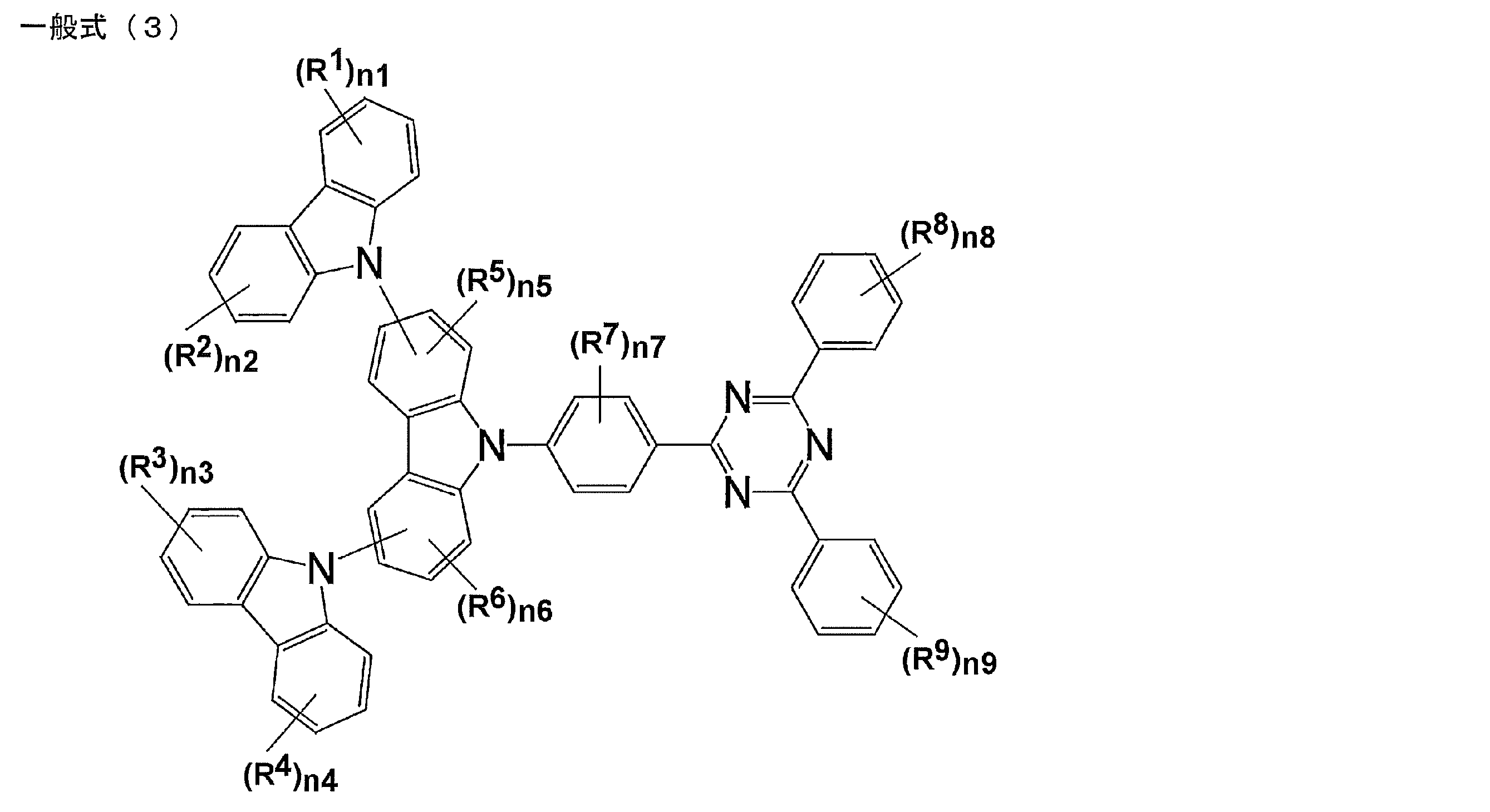
R5およびR6は各々独立に置換もしくは無置換のアルキル基を表し、
R7、R8およびR9は各々独立に置換もしくは無置換のアリール基、置換もしくは無置換のアルキル基、または置換もしくは無置換のカルバゾリル基を表し、
n1~n4およびn7は各々独立に0~4のいずれかの整数を表し、
n5およびn6は0~3のいずれかの整数を表し、
n8およびn9は各々独立に0~5のいずれかの整数を表す。
n1~n9が2以上の整数であるとき、各n1~n9に対応する複数のR1~R9はそれぞれ互いに同一であっても異なっていてもよい。] - 遅延蛍光を放射することを特徴とする請求項1~3のいずれか1項に記載の発光材料。
- 一般式(2)におけるn6が0であることを特徴とする請求項2または4に記載の発光材料。
- 一般式(2)におけるn1が1~4のいずれかの整数であることを特徴とする請求項2、4、5のいずれか1項に記載の発光材料。
- 一般式(2)におけるカルバゾリル基の3位にR1が結合していることを特徴とする請求項6に記載の発光材料。
- 一般式(2)におけるn2が1~4のいずれかの整数であることを特徴とする請求項6または7に記載の発光材料。
- 一般式(2)におけるカルバゾリル基の6位にR2が結合していることを特徴とする請求項8に記載の発光材料。
- 一般式(1)および(2)におけるR1およびR2が各々独立に置換もしくは無置換の9-カルバゾリル基、置換もしくは無置換のフェニル基、置換もしくは無置換のピリジル基、炭素数1~6のアルキル基、炭素数5~7のシクロアルキル基であることを特徴とする請求項1、2、4~9のいずれか1項に記載の発光材料。
- 一般式(1)および(2)におけるR1およびR2が各々独立に9-カルバゾリル基、フェニル基、トリル基、ジメチルフェニル基、トリメチルフェニル基、ビフェニル基、ピリジル基、ピロリル基、tert-ブチル基、またはシクロヘキシル基であることを特徴とする請求項1、2、4~9のいずれか1項に記載の発光材料。
- 一般式(2)におけるn1とn2がいずれも0であることを特徴とする請求項2、4、5のいずれか1項に記載の発光材料。
- 一般式(3)におけるn1~n4の少なくとも1つが1~4のいずれかの整数であることを特徴とする請求項3または4に記載の発光材料。
- 一般式(3)におけるn1~n4が各々独立に1~4のいずれかの整数であることを特徴とする請求項3または4に記載の発光材料。
- 一般式(3)におけるR1~R4が各々独立に置換もしくは無置換の9-カルバゾリル基、置換もしくは無置換のフェニル基、置換もしくは無置換のピリジル基、炭素数1~6のアルキル基、炭素数5~7のシクロアルキル基であることを特徴とする請求項3、4、13、14のいずれか1項に記載の発光材料。
- 一般式(3)におけるR1~R4が各々独立に9-カルバゾリル基、フェニル基、トリル基、ジメチルフェニル基、トリメチルフェニル基、ビフェニル基、ピリジル基、ピロリル基、tert-ブチル基、またはシクロヘキシル基であることを特徴とする請求項3、4、13、14のいずれか1項に記載の発光材料。
- 一般式(3)におけるn5とn6がいずれも0であることを特徴とする請求項3、4、13~16のいずれか1項に記載の発光材料。
- 一般式(1)~(3)におけるn7、n8およびn9がいずれも0であることを特徴とする請求項1~17のいずれか1項に記載の発光材料。
- 下記一般式(1)で表される構造を有する遅延蛍光体。

R5およびR6は各々独立に置換もしくは無置換のアルキル基を表し、
R7、R8およびR9は各々独立に置換もしくは無置換のアリール基、置換もしくは無置換のアルキル基、または置換もしくは無置換のカルバゾリル基を表し、
R10はカルバゾリル基を表し、該カルバゾリル基は、置換もしくは無置換のカルバゾリル基、置換もしくは無置換のアリール基、置換もしくは無置換のヘテロアリール基、置換もしくは無置換のアルキル基、または置換もしくは無置換のシクロアルキル基で置換されていてもよく、
n1、n2、n6およびn7は各々独立に0~4のいずれかの整数を表し、
n5は0~3のいずれかの整数を表し、
n8およびn9は各々独立に0~5のいずれかの整数を表す。
n10は0または1を表し、
n1、n2およびn5~n9が2以上の整数であるとき、各n1、n2およびn5~n9に対応する複数のR1、R2およびR5~R9はそれぞれ互いに同一であっても異なっていてもよい。] - 下記一般式(2)で表される化合物。

R5およびR6は各々独立に置換もしくは無置換のアルキル基を表し、
R7、R8およびR9は各々独立に置換もしくは無置換のアリール基、置換もしくは無置換のアルキル基、または置換もしくは無置換のカルバゾリル基を表し、
n1、n2、n6およびn7は各々独立に0~4のいずれかの整数を表し、
n5は0~3のいずれかの整数を表し、
n8およびn9は各々独立に0~5のいずれかの整数を表す。
n1、n2、n5~n9が2以上の整数であるとき、各n1、n2、n5~n9に対応する複数のR1、R2、R5~R9はそれぞれ互いに同一であっても異なっていてもよい。] - 下記一般式(4)で表される化合物。

R15およびR16は各々独立にアルキル基を表し、
R17、R18およびR19は各々独立に置換もしくは無置換のアリール基、置換もしくは無置換のアルキル基、または置換もしくは無置換のカルバゾリル基を表し、
n11~n14およびn17は各々独立に0~4のいずれかの整数を表し、
n15およびn16は0~3のいずれかの整数を表し、
n18およびn19は各々独立に0~5のいずれかの整数を表す。
ただし、n11~n14の少なくとも1つは1~4のいずれかの整数である。
n11~n19が2以上の整数であるとき、各n11~n19に対応する複数のR11~R19はそれぞれ互いに同一であっても異なっていてもよい。] - 請求項1~18のいずれか1項に記載の発光材料を含む発光層を基板上に有することを特徴とする有機発光素子。
- 遅延蛍光を放射することを特徴とする請求項22に記載の有機発光素子。
- 有機エレクトロルミネッセンス素子であることを特徴とする請求項22または23に記載の有機発光素子。
Priority Applications (4)
| Application Number | Priority Date | Filing Date | Title |
|---|---|---|---|
| CN201480005878.2A CN105121595B (zh) | 2013-01-23 | 2014-01-22 | 发光材料及使用其的有机发光元件 |
| EP14742808.0A EP2949724B1 (en) | 2013-01-23 | 2014-01-22 | Light emitting material and organic light emitting element using same |
| KR1020157022416A KR102151294B1 (ko) | 2013-01-23 | 2014-01-22 | 발광 재료 및 그것을 사용한 유기 발광 소자 |
| US14/762,269 US20150357582A1 (en) | 2013-01-23 | 2014-01-22 | Light emitting material and organic light emitting device using same |
Applications Claiming Priority (4)
| Application Number | Priority Date | Filing Date | Title |
|---|---|---|---|
| JP2013-010154 | 2013-01-23 | ||
| JP2013010154A JP6249151B2 (ja) | 2013-01-23 | 2013-01-23 | 発光材料およびそれを用いた有機発光素子 |
| JP2013010153A JP6249150B2 (ja) | 2013-01-23 | 2013-01-23 | 発光材料およびそれを用いた有機発光素子 |
| JP2013-010153 | 2013-01-23 |
Publications (1)
| Publication Number | Publication Date |
|---|---|
| WO2014115743A1 true WO2014115743A1 (ja) | 2014-07-31 |
Family
ID=51227534
Family Applications (1)
| Application Number | Title | Priority Date | Filing Date |
|---|---|---|---|
| PCT/JP2014/051184 WO2014115743A1 (ja) | 2013-01-23 | 2014-01-22 | 発光材料およびそれを用いた有機発光素子 |
Country Status (6)
| Country | Link |
|---|---|
| US (1) | US20150357582A1 (ja) |
| EP (1) | EP2949724B1 (ja) |
| KR (1) | KR102151294B1 (ja) |
| CN (1) | CN105121595B (ja) |
| TW (1) | TWI637037B (ja) |
| WO (1) | WO2014115743A1 (ja) |
Cited By (21)
| Publication number | Priority date | Publication date | Assignee | Title |
|---|---|---|---|---|
| WO2015072470A1 (ja) * | 2013-11-12 | 2015-05-21 | 国立大学法人九州大学 | 発光材料、並びに、これを用いた遅延蛍光体および有機発光素子 |
| TWI586655B (zh) * | 2014-10-30 | 2017-06-11 | Lg 化學股份有限公司 | 環狀化合物及含有該環狀化合物的有機發光元件 |
| JP2018111751A (ja) * | 2017-01-10 | 2018-07-19 | 国立大学法人九州大学 | 発光材料、化合物および有機発光素子 |
| WO2019049225A1 (ja) | 2017-09-06 | 2019-03-14 | 住友化学株式会社 | 発光素子 |
| WO2020076796A1 (en) | 2018-10-09 | 2020-04-16 | Kyulux, Inc. | Novel composition of matter for use in organic light-emitting diodes |
| US10651392B2 (en) | 2015-09-30 | 2020-05-12 | Samsung Electronics Co., Ltd. | Organic light-emitting device |
| WO2021157642A1 (ja) | 2020-02-04 | 2021-08-12 | 株式会社Kyulux | ホスト材料、組成物および有機発光素子 |
| US11101440B2 (en) | 2015-07-01 | 2021-08-24 | Kyushu University, National University Corporation | Organic electroluminescent device |
| WO2021235549A1 (ja) | 2020-05-22 | 2021-11-25 | 株式会社Kyulux | 化合物、発光材料および発光素子 |
| WO2022025248A1 (ja) | 2020-07-31 | 2022-02-03 | 株式会社Kyulux | 化合物、発光材料および発光素子 |
| US11335872B2 (en) | 2016-09-06 | 2022-05-17 | Kyulux, Inc. | Organic light-emitting device |
| WO2022168956A1 (ja) | 2021-02-04 | 2022-08-11 | 株式会社Kyulux | 化合物、発光材料および有機発光素子 |
| US11476435B2 (en) | 2017-08-24 | 2022-10-18 | Kyushu University, National University Corporation | Film and organic light-emitting device containing perovskite-type compound and organic light-emitting material |
| US11482679B2 (en) | 2017-05-23 | 2022-10-25 | Kyushu University, National University Corporation | Compound, light-emitting lifetime lengthening agent, use of n-type compound, film and light-emitting device |
| US11485706B2 (en) | 2018-09-11 | 2022-11-01 | Universal Display Corporation | Organic electroluminescent materials and devices |
| WO2022244503A1 (ja) | 2021-05-20 | 2022-11-24 | 株式会社Kyulux | 有機発光素子 |
| WO2022270602A1 (ja) | 2021-06-23 | 2022-12-29 | 株式会社Kyulux | 有機発光素子および膜 |
| WO2022270354A1 (ja) | 2021-06-23 | 2022-12-29 | 株式会社Kyulux | 化合物、発光材料および有機発光素子 |
| WO2023282224A1 (ja) | 2021-07-06 | 2023-01-12 | 株式会社Kyulux | 有機発光素子およびその設計方法 |
| WO2023053835A1 (ja) | 2021-09-28 | 2023-04-06 | 株式会社Kyulux | 化合物、組成物、ホスト材料、電子障壁材料および有機発光素子 |
| US11930654B2 (en) | 2017-07-06 | 2024-03-12 | Kyulux, Inc. | Organic light-emitting element |
Families Citing this family (10)
| Publication number | Priority date | Publication date | Assignee | Title |
|---|---|---|---|---|
| US9209411B2 (en) | 2012-12-07 | 2015-12-08 | Universal Display Corporation | Organic electroluminescent materials and devices |
| CN107880030B (zh) * | 2016-09-30 | 2021-03-30 | 中节能万润股份有限公司 | 以三嗪为核心的化合物及有机电致发光器件 |
| CN108239072A (zh) * | 2016-12-27 | 2018-07-03 | 江苏三月光电科技有限公司 | 一种三嗪衍生物及其在有机电致发光器件上的应用 |
| CN108239070B (zh) * | 2016-12-27 | 2021-06-15 | 中节能万润股份有限公司 | 一种以三联咔唑为核心的化合物及其在有机电致发光器件上的应用 |
| CN108409716A (zh) | 2017-02-10 | 2018-08-17 | 三星显示有限公司 | 杂环化合物以及包括该杂环化合物的有机发光装置 |
| US11706977B2 (en) | 2018-01-11 | 2023-07-18 | Samsung Electronics Co., Ltd. | Heterocyclic compound, composition including the same, and organic light-emitting device including the heterocyclic compound |
| CN112898275A (zh) * | 2019-12-04 | 2021-06-04 | 三星电子株式会社 | 化合物、组合物、液体组合物、用于有机电致发光器件的材料和有机电致发光器件 |
| CN113493446A (zh) * | 2020-04-03 | 2021-10-12 | 南京高光半导体材料有限公司 | 一种基于咔唑基的有机电致发光化合物及有机电致发光器件 |
| CN113248664B (zh) * | 2021-06-21 | 2023-03-14 | 贵溪穿越光电科技有限公司 | 一种用于OLEDs显示屏中电致发光材料的制备方法 |
| CN115073428A (zh) * | 2022-07-29 | 2022-09-20 | 阜阳欣奕华材料科技有限公司 | 一种三嗪类组合物及其制备方法和应用 |
Citations (4)
| Publication number | Priority date | Publication date | Assignee | Title |
|---|---|---|---|---|
| JP2002193952A (ja) | 2000-12-25 | 2002-07-10 | Fuji Photo Film Co Ltd | 新規含窒素へテロ環化合物、発光素子材料およびそれらを使用した発光素子 |
| JP2009021336A (ja) | 2007-07-11 | 2009-01-29 | Konica Minolta Holdings Inc | 有機エレクトロルミネッセンス素子、表示装置及び照明装置 |
| WO2011049325A2 (en) * | 2009-10-21 | 2011-04-28 | Cheil Industries Inc. | Novel compound for organic photoelectric device and organic photoelectric device including the same |
| WO2012077902A2 (ko) | 2010-12-08 | 2012-06-14 | 제일모직 주식회사 | 유기광전자소자용 화합물, 이를 포함하는 유기발광소자 및 상기 유기발광소자를 포함하는 표시장치 |
Family Cites Families (4)
| Publication number | Priority date | Publication date | Assignee | Title |
|---|---|---|---|---|
| EP2374848B1 (en) * | 2010-04-09 | 2013-01-16 | Clariant Finance (BVI) Limited | New magenta quinacridone pigments |
| KR101432599B1 (ko) * | 2010-08-04 | 2014-08-21 | 제일모직주식회사 | 유기광전소자용 화합물 및 이를 포함하는 유기광전소자 |
| KR20140096182A (ko) * | 2012-05-02 | 2014-08-04 | 롬엔드하스전자재료코리아유한회사 | 신규한 유기 전계 발광 화합물 및 이를 채용하고 있는 유기 전계 발광 소자 |
| CN107325050A (zh) * | 2012-12-28 | 2017-11-07 | 出光兴产株式会社 | 有机电致发光元件 |
-
2014
- 2014-01-22 KR KR1020157022416A patent/KR102151294B1/ko active IP Right Grant
- 2014-01-22 EP EP14742808.0A patent/EP2949724B1/en active Active
- 2014-01-22 CN CN201480005878.2A patent/CN105121595B/zh active Active
- 2014-01-22 WO PCT/JP2014/051184 patent/WO2014115743A1/ja active Application Filing
- 2014-01-22 US US14/762,269 patent/US20150357582A1/en not_active Abandoned
- 2014-01-23 TW TW103102532A patent/TWI637037B/zh active
Patent Citations (4)
| Publication number | Priority date | Publication date | Assignee | Title |
|---|---|---|---|---|
| JP2002193952A (ja) | 2000-12-25 | 2002-07-10 | Fuji Photo Film Co Ltd | 新規含窒素へテロ環化合物、発光素子材料およびそれらを使用した発光素子 |
| JP2009021336A (ja) | 2007-07-11 | 2009-01-29 | Konica Minolta Holdings Inc | 有機エレクトロルミネッセンス素子、表示装置及び照明装置 |
| WO2011049325A2 (en) * | 2009-10-21 | 2011-04-28 | Cheil Industries Inc. | Novel compound for organic photoelectric device and organic photoelectric device including the same |
| WO2012077902A2 (ko) | 2010-12-08 | 2012-06-14 | 제일모직 주식회사 | 유기광전자소자용 화합물, 이를 포함하는 유기발광소자 및 상기 유기발광소자를 포함하는 표시장치 |
Non-Patent Citations (7)
| Title |
|---|
| APPL. PHYS. LETT., vol. 101, 2012, pages 093306 |
| AYATAKA ENDO ET AL.: "Efficient up-conversion of triplet excitons into a singlet state and its application for organic light emitting diodes", APPLIED PHYSICS LETTERS, vol. 98, 1 January 2011 (2011-01-01), pages 83302 - 83302-3, XP012140060, DOI: 10.1063/1.3558906 * |
| HIROKI UOYAMA ET AL.: "Highly efficient organic light-emitting diodes from delayed fluorescence", NATURE, vol. 492, 13 December 2012 (2012-12-13), pages 234 - 238, XP055048388, DOI: 10.1038/NATURE11687 * |
| HIRONORI KAJI ET AL.: "Fabrication and Analysis of Organic LEDs and Solar Cells", IEICE TECHNICAL REPORT, vol. 113, no. 18, 2013, pages 43 - 48, XP008180152 * |
| KENICHI GOUSHI ET AL.: "Organic light-emitting diodes employing efficient reverse intersystem crossing for triplet-to-singlet state conversion", NATURE PHOTONICS, vol. 6, 1 January 2012 (2012-01-01), pages 253 - 258, XP055133808, DOI: 10.1038/NPHOTON.2012.31 * |
| See also references of EP2949724A4 |
| SEREVICIUS T ET AL.: "Enhanced electroluminescence based on thermally activated delayed fluorescence from a carbazole -triazine derivative", PHYSICAL CHEMISTRY CHEMICAL PHYSICS, vol. 15, no. 38, 1 January 2013 (2013-01-01), pages 15850 - 15855, XP055202583, DOI: 10.1039/C3CP52255E * |
Cited By (25)
| Publication number | Priority date | Publication date | Assignee | Title |
|---|---|---|---|---|
| US11101433B2 (en) | 2013-11-12 | 2021-08-24 | Kyulux, Inc. | Light-emitting material, and delayed fluorescent emitter and organic light-emitting device using same |
| WO2015072470A1 (ja) * | 2013-11-12 | 2015-05-21 | 国立大学法人九州大学 | 発光材料、並びに、これを用いた遅延蛍光体および有機発光素子 |
| US10431748B2 (en) | 2014-10-30 | 2019-10-01 | Lg Chem, Ltd. | Cyclic compound and organic light-emitting element comprising same |
| TWI586655B (zh) * | 2014-10-30 | 2017-06-11 | Lg 化學股份有限公司 | 環狀化合物及含有該環狀化合物的有機發光元件 |
| US11101440B2 (en) | 2015-07-01 | 2021-08-24 | Kyushu University, National University Corporation | Organic electroluminescent device |
| US10651392B2 (en) | 2015-09-30 | 2020-05-12 | Samsung Electronics Co., Ltd. | Organic light-emitting device |
| US11335872B2 (en) | 2016-09-06 | 2022-05-17 | Kyulux, Inc. | Organic light-emitting device |
| JP2018111751A (ja) * | 2017-01-10 | 2018-07-19 | 国立大学法人九州大学 | 発光材料、化合物および有機発光素子 |
| US11482679B2 (en) | 2017-05-23 | 2022-10-25 | Kyushu University, National University Corporation | Compound, light-emitting lifetime lengthening agent, use of n-type compound, film and light-emitting device |
| US11930654B2 (en) | 2017-07-06 | 2024-03-12 | Kyulux, Inc. | Organic light-emitting element |
| US11476435B2 (en) | 2017-08-24 | 2022-10-18 | Kyushu University, National University Corporation | Film and organic light-emitting device containing perovskite-type compound and organic light-emitting material |
| WO2019049225A1 (ja) | 2017-09-06 | 2019-03-14 | 住友化学株式会社 | 発光素子 |
| US11939293B2 (en) | 2018-09-11 | 2024-03-26 | Universal Display Corporation | Organic electroluminescent materials and devices |
| US11485706B2 (en) | 2018-09-11 | 2022-11-01 | Universal Display Corporation | Organic electroluminescent materials and devices |
| WO2020076796A1 (en) | 2018-10-09 | 2020-04-16 | Kyulux, Inc. | Novel composition of matter for use in organic light-emitting diodes |
| WO2021157642A1 (ja) | 2020-02-04 | 2021-08-12 | 株式会社Kyulux | ホスト材料、組成物および有機発光素子 |
| WO2021157593A1 (ja) | 2020-02-04 | 2021-08-12 | 株式会社Kyulux | 組成物、膜、有機発光素子、発光組成物を提供する方法およびプログラム |
| WO2021235549A1 (ja) | 2020-05-22 | 2021-11-25 | 株式会社Kyulux | 化合物、発光材料および発光素子 |
| WO2022025248A1 (ja) | 2020-07-31 | 2022-02-03 | 株式会社Kyulux | 化合物、発光材料および発光素子 |
| WO2022168956A1 (ja) | 2021-02-04 | 2022-08-11 | 株式会社Kyulux | 化合物、発光材料および有機発光素子 |
| WO2022244503A1 (ja) | 2021-05-20 | 2022-11-24 | 株式会社Kyulux | 有機発光素子 |
| WO2022270602A1 (ja) | 2021-06-23 | 2022-12-29 | 株式会社Kyulux | 有機発光素子および膜 |
| WO2022270354A1 (ja) | 2021-06-23 | 2022-12-29 | 株式会社Kyulux | 化合物、発光材料および有機発光素子 |
| WO2023282224A1 (ja) | 2021-07-06 | 2023-01-12 | 株式会社Kyulux | 有機発光素子およびその設計方法 |
| WO2023053835A1 (ja) | 2021-09-28 | 2023-04-06 | 株式会社Kyulux | 化合物、組成物、ホスト材料、電子障壁材料および有機発光素子 |
Also Published As
| Publication number | Publication date |
|---|---|
| CN105121595B (zh) | 2018-02-02 |
| TW201435044A (zh) | 2014-09-16 |
| US20150357582A1 (en) | 2015-12-10 |
| EP2949724A4 (en) | 2016-06-29 |
| KR102151294B1 (ko) | 2020-09-02 |
| CN105121595A (zh) | 2015-12-02 |
| KR20150108899A (ko) | 2015-09-30 |
| EP2949724A1 (en) | 2015-12-02 |
| TWI637037B (zh) | 2018-10-01 |
| EP2949724B1 (en) | 2020-06-17 |
Similar Documents
| Publication | Publication Date | Title |
|---|---|---|
| WO2014115743A1 (ja) | 発光材料およびそれを用いた有機発光素子 | |
| JP6277182B2 (ja) | 化合物、発光材料および有機発光素子 | |
| JP6263524B2 (ja) | 化合物、発光材料および有機発光素子 | |
| JP5594750B2 (ja) | 化合物、発光材料および有機発光素子 | |
| JP6326050B2 (ja) | 化合物、発光材料および有機発光素子 | |
| KR102168905B1 (ko) | 유기 발광 소자 그리고 그것에 사용하는 발광 재료 및 화합물 | |
| JP6318155B2 (ja) | 化合物、発光材料および有機発光素子 | |
| JP6391570B2 (ja) | 赤色発光材料、有機発光素子および化合物 | |
| JP6225111B2 (ja) | 発光材料、化合物、およびそれらを用いた有機発光素子 | |
| JP6262711B2 (ja) | 化合物、発光材料および有機発光素子 | |
| JP5366106B1 (ja) | 有機発光素子ならびにそれに用いる発光材料および化合物 | |
| JP6383538B2 (ja) | 発光材料、有機発光素子および化合物 | |
| JP6293417B2 (ja) | 化合物、発光材料および有機発光素子 | |
| WO2015133501A1 (ja) | 発光材料、有機発光素子および化合物 | |
| JP6249150B2 (ja) | 発光材料およびそれを用いた有機発光素子 | |
| WO2013081088A1 (ja) | 有機発光素子ならびにそれに用いる遅延蛍光材料および化合物 | |
| JP2017119663A (ja) | 化合物、発光材料および有機発光素子 | |
| JP6647514B2 (ja) | 有機発光素子ならびにそれに用いる発光材料および化合物 | |
| WO2014126076A1 (ja) | 化合物、発光材料および有機発光素子 | |
| JP6249151B2 (ja) | 発光材料およびそれを用いた有機発光素子 | |
| JP2018111751A (ja) | 発光材料、化合物および有機発光素子 | |
| JP2016084283A (ja) | 化合物、発光材料および有機発光素子 | |
| JP2016084284A (ja) | 化合物、発光材料および有機発光素子 |
Legal Events
| Date | Code | Title | Description |
|---|---|---|---|
| 121 | Ep: the epo has been informed by wipo that ep was designated in this application |
Ref document number: 14742808 Country of ref document: EP Kind code of ref document: A1 |
|
| WWE | Wipo information: entry into national phase |
Ref document number: 14762269 Country of ref document: US |
|
| NENP | Non-entry into the national phase |
Ref country code: DE |
|
| WWE | Wipo information: entry into national phase |
Ref document number: 2014742808 Country of ref document: EP |
|
| ENP | Entry into the national phase |
Ref document number: 20157022416 Country of ref document: KR Kind code of ref document: A |