WO2014106930A1 - 高周波回路用基板 - Google Patents
高周波回路用基板 Download PDFInfo
- Publication number
- WO2014106930A1 WO2014106930A1 PCT/JP2013/084122 JP2013084122W WO2014106930A1 WO 2014106930 A1 WO2014106930 A1 WO 2014106930A1 JP 2013084122 W JP2013084122 W JP 2013084122W WO 2014106930 A1 WO2014106930 A1 WO 2014106930A1
- Authority
- WO
- WIPO (PCT)
- Prior art keywords
- copper foil
- layer
- frequency circuit
- polyimide
- circuit board
- Prior art date
- Legal status (The legal status is an assumption and is not a legal conclusion. Google has not performed a legal analysis and makes no representation as to the accuracy of the status listed.)
- Ceased
Links
Classifications
-
- B—PERFORMING OPERATIONS; TRANSPORTING
- B32—LAYERED PRODUCTS
- B32B—LAYERED PRODUCTS, i.e. PRODUCTS BUILT-UP OF STRATA OF FLAT OR NON-FLAT, e.g. CELLULAR OR HONEYCOMB, FORM
- B32B15/00—Layered products comprising a layer of metal
- B32B15/04—Layered products comprising a layer of metal comprising metal as the main or only constituent of a layer, which is next to another layer of the same or of a different material
- B32B15/08—Layered products comprising a layer of metal comprising metal as the main or only constituent of a layer, which is next to another layer of the same or of a different material of synthetic resin
-
- B—PERFORMING OPERATIONS; TRANSPORTING
- B32—LAYERED PRODUCTS
- B32B—LAYERED PRODUCTS, i.e. PRODUCTS BUILT-UP OF STRATA OF FLAT OR NON-FLAT, e.g. CELLULAR OR HONEYCOMB, FORM
- B32B15/00—Layered products comprising a layer of metal
- B32B15/20—Layered products comprising a layer of metal comprising aluminium or copper
-
- B—PERFORMING OPERATIONS; TRANSPORTING
- B32—LAYERED PRODUCTS
- B32B—LAYERED PRODUCTS, i.e. PRODUCTS BUILT-UP OF STRATA OF FLAT OR NON-FLAT, e.g. CELLULAR OR HONEYCOMB, FORM
- B32B27/00—Layered products comprising a layer of synthetic resin
- B32B27/06—Layered products comprising a layer of synthetic resin as the main or only constituent of a layer, which is next to another layer of the same or of a different material
- B32B27/08—Layered products comprising a layer of synthetic resin as the main or only constituent of a layer, which is next to another layer of the same or of a different material of synthetic resin
-
- B—PERFORMING OPERATIONS; TRANSPORTING
- B32—LAYERED PRODUCTS
- B32B—LAYERED PRODUCTS, i.e. PRODUCTS BUILT-UP OF STRATA OF FLAT OR NON-FLAT, e.g. CELLULAR OR HONEYCOMB, FORM
- B32B27/00—Layered products comprising a layer of synthetic resin
- B32B27/28—Layered products comprising a layer of synthetic resin comprising synthetic resins not wholly covered by any one of the sub-groups B32B27/30 - B32B27/42
- B32B27/281—Layered products comprising a layer of synthetic resin comprising synthetic resins not wholly covered by any one of the sub-groups B32B27/30 - B32B27/42 comprising polyimides
-
- C—CHEMISTRY; METALLURGY
- C08—ORGANIC MACROMOLECULAR COMPOUNDS; THEIR PREPARATION OR CHEMICAL WORKING-UP; COMPOSITIONS BASED THEREON
- C08G—MACROMOLECULAR COMPOUNDS OBTAINED OTHERWISE THAN BY REACTIONS ONLY INVOLVING UNSATURATED CARBON-TO-CARBON BONDS
- C08G73/00—Macromolecular compounds obtained by reactions forming a linkage containing nitrogen with or without oxygen or carbon in the main chain of the macromolecule, not provided for in groups C08G12/00 - C08G71/00
- C08G73/06—Polycondensates having nitrogen-containing heterocyclic rings in the main chain of the macromolecule
- C08G73/10—Polyimides; Polyester-imides; Polyamide-imides; Polyamide acids or similar polyimide precursors
- C08G73/1042—Copolyimides derived from at least two different tetracarboxylic compounds or two different diamino compounds
-
- C—CHEMISTRY; METALLURGY
- C08—ORGANIC MACROMOLECULAR COMPOUNDS; THEIR PREPARATION OR CHEMICAL WORKING-UP; COMPOSITIONS BASED THEREON
- C08G—MACROMOLECULAR COMPOUNDS OBTAINED OTHERWISE THAN BY REACTIONS ONLY INVOLVING UNSATURATED CARBON-TO-CARBON BONDS
- C08G73/00—Macromolecular compounds obtained by reactions forming a linkage containing nitrogen with or without oxygen or carbon in the main chain of the macromolecule, not provided for in groups C08G12/00 - C08G71/00
- C08G73/06—Polycondensates having nitrogen-containing heterocyclic rings in the main chain of the macromolecule
- C08G73/10—Polyimides; Polyester-imides; Polyamide-imides; Polyamide acids or similar polyimide precursors
- C08G73/1046—Polyimides containing oxygen in the form of ether bonds in the main chain
- C08G73/105—Polyimides containing oxygen in the form of ether bonds in the main chain with oxygen only in the diamino moiety
-
- C—CHEMISTRY; METALLURGY
- C08—ORGANIC MACROMOLECULAR COMPOUNDS; THEIR PREPARATION OR CHEMICAL WORKING-UP; COMPOSITIONS BASED THEREON
- C08G—MACROMOLECULAR COMPOUNDS OBTAINED OTHERWISE THAN BY REACTIONS ONLY INVOLVING UNSATURATED CARBON-TO-CARBON BONDS
- C08G73/00—Macromolecular compounds obtained by reactions forming a linkage containing nitrogen with or without oxygen or carbon in the main chain of the macromolecule, not provided for in groups C08G12/00 - C08G71/00
- C08G73/06—Polycondensates having nitrogen-containing heterocyclic rings in the main chain of the macromolecule
- C08G73/10—Polyimides; Polyester-imides; Polyamide-imides; Polyamide acids or similar polyimide precursors
- C08G73/1067—Wholly aromatic polyimides, i.e. having both tetracarboxylic and diamino moieties aromatically bound
- C08G73/1071—Wholly aromatic polyimides containing oxygen in the form of ether bonds in the main chain
-
- C—CHEMISTRY; METALLURGY
- C08—ORGANIC MACROMOLECULAR COMPOUNDS; THEIR PREPARATION OR CHEMICAL WORKING-UP; COMPOSITIONS BASED THEREON
- C08L—COMPOSITIONS OF MACROMOLECULAR COMPOUNDS
- C08L79/00—Compositions of macromolecular compounds obtained by reactions forming in the main chain of the macromolecule a linkage containing nitrogen with or without oxygen or carbon only, not provided for in groups C08L61/00 - C08L77/00
- C08L79/04—Polycondensates having nitrogen-containing heterocyclic rings in the main chain; Polyhydrazides; Polyamide acids or similar polyimide precursors
- C08L79/08—Polyimides; Polyester-imides; Polyamide-imides; Polyamide acids or similar polyimide precursors
-
- H—ELECTRICITY
- H05—ELECTRIC TECHNIQUES NOT OTHERWISE PROVIDED FOR
- H05K—PRINTED CIRCUITS; CASINGS OR CONSTRUCTIONAL DETAILS OF ELECTRIC APPARATUS; MANUFACTURE OF ASSEMBLAGES OF ELECTRICAL COMPONENTS
- H05K3/00—Apparatus or processes for manufacturing printed circuits
- H05K3/38—Improvement of the adhesion between the insulating substrate and the metal
- H05K3/386—Improvement of the adhesion between the insulating substrate and the metal by the use of an organic polymeric bonding layer, e.g. adhesive
-
- B—PERFORMING OPERATIONS; TRANSPORTING
- B32—LAYERED PRODUCTS
- B32B—LAYERED PRODUCTS, i.e. PRODUCTS BUILT-UP OF STRATA OF FLAT OR NON-FLAT, e.g. CELLULAR OR HONEYCOMB, FORM
- B32B2307/00—Properties of the layers or laminate
- B32B2307/50—Properties of the layers or laminate having particular mechanical properties
- B32B2307/538—Roughness
-
- H—ELECTRICITY
- H05—ELECTRIC TECHNIQUES NOT OTHERWISE PROVIDED FOR
- H05K—PRINTED CIRCUITS; CASINGS OR CONSTRUCTIONAL DETAILS OF ELECTRIC APPARATUS; MANUFACTURE OF ASSEMBLAGES OF ELECTRICAL COMPONENTS
- H05K1/00—Printed circuits
- H05K1/02—Details
- H05K1/03—Use of materials for the substrate
- H05K1/0313—Organic insulating material
- H05K1/0353—Organic insulating material consisting of two or more materials, e.g. two or more polymers, polymer + filler, + reinforcement
- H05K1/036—Multilayers with layers of different types
-
- H—ELECTRICITY
- H05—ELECTRIC TECHNIQUES NOT OTHERWISE PROVIDED FOR
- H05K—PRINTED CIRCUITS; CASINGS OR CONSTRUCTIONAL DETAILS OF ELECTRIC APPARATUS; MANUFACTURE OF ASSEMBLAGES OF ELECTRICAL COMPONENTS
- H05K2201/00—Indexing scheme relating to printed circuits covered by H05K1/00
- H05K2201/01—Dielectrics
- H05K2201/0137—Materials
- H05K2201/015—Fluoropolymer, e.g. polytetrafluoroethylene [PTFE]
-
- H—ELECTRICITY
- H05—ELECTRIC TECHNIQUES NOT OTHERWISE PROVIDED FOR
- H05K—PRINTED CIRCUITS; CASINGS OR CONSTRUCTIONAL DETAILS OF ELECTRIC APPARATUS; MANUFACTURE OF ASSEMBLAGES OF ELECTRICAL COMPONENTS
- H05K2201/00—Indexing scheme relating to printed circuits covered by H05K1/00
- H05K2201/01—Dielectrics
- H05K2201/0137—Materials
- H05K2201/0154—Polyimide
-
- H—ELECTRICITY
- H05—ELECTRIC TECHNIQUES NOT OTHERWISE PROVIDED FOR
- H05K—PRINTED CIRCUITS; CASINGS OR CONSTRUCTIONAL DETAILS OF ELECTRIC APPARATUS; MANUFACTURE OF ASSEMBLAGES OF ELECTRICAL COMPONENTS
- H05K2201/00—Indexing scheme relating to printed circuits covered by H05K1/00
- H05K2201/01—Dielectrics
- H05K2201/0183—Dielectric layers
- H05K2201/0195—Dielectric or adhesive layers comprising a plurality of layers, e.g. in a multilayer structure
-
- H—ELECTRICITY
- H05—ELECTRIC TECHNIQUES NOT OTHERWISE PROVIDED FOR
- H05K—PRINTED CIRCUITS; CASINGS OR CONSTRUCTIONAL DETAILS OF ELECTRIC APPARATUS; MANUFACTURE OF ASSEMBLAGES OF ELECTRICAL COMPONENTS
- H05K3/00—Apparatus or processes for manufacturing printed circuits
- H05K3/02—Apparatus or processes for manufacturing printed circuits in which the conductive material is applied to the surface of the insulating support and is thereafter removed from such areas of the surface which are not intended for current conducting or shielding
- H05K3/022—Processes for manufacturing precursors of printed circuits, i.e. copper-clad substrates
Definitions
- the present invention relates to a high-frequency circuit board that is excellent in high-frequency transmission characteristics, has sufficient adhesion to a resin layer, and has excellent solder reflow resistance.
- a laminate in which a polyimide insulating layer is formed on a copper foil is widely used for flexible substrates from the viewpoint of heat resistance and mechanical strength.
- a material having a small transmission loss during high-speed transmission has been demanded.
- polyimide does not have a high adhesive force with a metal, and thus it is necessary to roughen the surface of the metal in order to improve the adhesion.
- the signal easily propagates on the surface of the metal at a high frequency of 1 GHz or more (skin effect).
- the unevenness of the surface of the metal foil that becomes the transmission line is large, the electric signal is not in the conductor but in the unevenness.
- Patent Document 1 a flexible copper-clad laminate in which the surface roughness of the copper foil is 0.6 to 0.7 ⁇ m is exemplified.
- an electric signal travels a depth of 0.5 ⁇ m from the metal surface, and the depth becomes shallower as the frequency becomes higher.
- the surface roughness of 0.6 to 0.7 ⁇ m as in Patent Document 1 is too large to reduce the transmission loss of high-frequency signals.
- Transmission loss is also affected by the dielectric properties of the dielectric.
- Polyimide is a resin having a relatively low dielectric loss tangent, but the dielectric constant is 3 to 4 which is the same level as that of an epoxy resin, and is never low.
- polyimide has high hygroscopicity, but when the resin absorbs moisture, the dielectric loss tangent tends to increase. Therefore, in order to improve transmission loss, it is necessary to reduce the hygroscopicity of the dielectric.
- Patent Document 2 describes a copper-clad laminate obtained by applying a polyamic acid having a specific molecular structure to a copper foil having a low surface roughness and imidizing the polyamic acid. It is limited to a single layer substrate composed of a polyimide layer.
- Patent Documents 3 and 4 as a layer structure for improving the dielectric characteristics and dimensional stability of an electronic circuit board, a fluororesin layer / polyimide resin layer / fluororesin layer laminated in this order, or a polyimide resin Although what laminated
- JP 2009-246201 A Japanese Patent No. 4412708 JP 2011-11456 A JP 2011-11457 A
- the present invention has been made in view of the above points, and can reduce electric signal transmission loss in a high-frequency circuit, and at the same time, has high adhesion between a copper foil and a resin layer, and has a dielectric constant and dielectric loss tangent. And it aims at providing the board
- the present inventors applied a solution containing a polyamic acid having a specific molecular structure on a copper foil having a low surface roughness, dried the solvent at a high temperature, and caused an imidization reaction to form a single layer substrate. After being obtained, the resin surfaces of this single-layer substrate are thermocompression-bonded via a fluororesin film, so that the adhesiveness is high even for a copper foil having a low surface roughness, dielectric constant, dielectric loss tangent, and hygroscopicity.
- the present invention has been completed by finding that a high-frequency circuit board having a low frequency can be obtained.
- the present invention relates to the following (1) to (3).
- (1) Copper foil / (B) Polyimide layer / (C) Fluororesin layer / (D) Polyimide layer / (E) A high frequency circuit board in which a copper foil is laminated in this order,
- the polyimide resin constituting the polyimide layer comprises the following components (a) to (c):
- High frequency circuit board (2) The high frequency circuit board according to (1), wherein the copper foil has a surface roughness Sa of 0.5 ⁇ m or less. (3) The high frequency circuit board according to the above (1) or (2), wherein the fluororesin constituting the fluororesin layer is a tetrafluoroethylene / perfluoroalkyl vinyl ether copolymer (PFA).
- PFA perfluoroalkyl vinyl ether copolymer
- the substrate for a high-frequency circuit of the present invention has very little transmission loss even in a high-frequency band, has high adhesion between the copper foil and the resin layer, and is excellent in dielectric properties and moisture absorption resistance.
- the copper foil used in the present invention preferably has a surface roughness Sa in the range of 0.5 ⁇ m or less, and more preferably in the range of 0.2 ⁇ m or less. If the surface roughness Sa exceeds 0.5 ⁇ m, the transmission loss increases and the practical performance may not be satisfied.
- the thickness of the copper foil is usually 5 to 50 ⁇ m, preferably 8 to 40 ⁇ m.
- Ra which is an arithmetic average of irregularities in two-dimensional linear shapes, has been generally used as the surface roughness, but it is difficult to say that it is an accurate value because the actual surface has a three-dimensional extent.
- Sa is an arithmetic average of unevenness in a three-dimensional space and has high accuracy.
- the copper foil surface may be an untreated copper foil surface, and the surface is a metal plating treatment, for example, a group consisting of nickel, iron, zinc, gold, silver, aluminum, chromium, titanium, palladium, and tin. It may be plated with one or more selected metals. Moreover, the surface of the untreated copper foil or the surface of the copper foil that has been subjected to metal plating may be surface-treated with a chemical such as a silane coupling agent.
- the metal plating treatment is preferably a metal plating treatment with one or more metals selected from nickel, iron, zinc, gold, and aluminum, and more preferably a metal plating treatment with nickel or aluminum. In some cases, metal plating treatment with one or more metals selected from the group consisting of nickel, iron, zinc, gold, and tin is preferable.
- the polyamic acid used in the present invention is obtained by reacting a diamine represented by the following formula (1), a specific aromatic diamine, and an aromatic tetrabasic acid dianhydride.
- n 0 or 1.
- diamine represented by the above formula (1) examples include diaminodiphenyl ethers such as 4,4′-diaminodiphenyl ether, 2,4′-diaminodiphenyl ether, and 3,4′-diaminodiphenyl ether; 1,3-bis (3- Bisaminophenoxybenzenes such as aminophenoxy) benzene and 1,3-bis (4-aminophenoxy) benzene;
- Examples of the specific aromatic diamine other than the diamine represented by the formula (1) include diaminodiphenylpropanes such as 4,4′-diaminodiphenylpropane and 3,4′-diaminodiphenylpropane; Bisanilines such as [1,3-phenylenebis (1-methylidene)] bisaniline, 4,4 ′-[1,4-phenylenebis (1-methylidene)] bisaniline; p-phenylenediamine, m-phenylenediamine, chloro Phenylenediamines such as p-phenylenediamine; diaminodiphenylmethanes such as 4,4′-diaminodiphenylmethane, 3,4′-diaminodiphenylmethane, 2,4′-diaminodiphenylmethane; 4,4′-diaminodiphenylsulfide, 3 , 4'-Diaminodiphenyl
- the aromatic tetrabasic acid dianhydride is not particularly limited as long as it is a compound dianhydride having a structure in which four carboxy groups are bonded to an aromatic ring.
- a part of the aromatic tetrabasic dianhydride may be used as a di (C1-C10) alkyl ester having the same or different mother nucleus.
- dimethylaminoethanol or the like is used as a catalyst, and aromatic tetrabasic dianhydride and methanol, ethanol, 1-propanol or the like is used. What is necessary is just to make it react with alcohols corresponding to the desired alkyl group.
- an aromatic tetrabasic dianhydride and water may be reacted using the same catalyst.
- the amount of catalyst used at this time is about 1 to 10 mol% with respect to the alcohol or water, and the amount of alcohol or water used is usually 2.4 to 4 of the aromatic tetrabasic dianhydride. 0.0 moles.
- the reaction temperature is usually 70 to 100 ° C., and the reaction time is usually 2 to 5 hours.
- a predetermined amount of the same or different mother nucleus can be separately mixed.
- the use ratio of the aromatic tetrabasic dianhydride and the aromatic tetrabasic acid di (C1 to C10) alkyl ester is 0.6 to 0.90 in terms of the molar ratio, while the latter is usually 0.10 to It is preferable that it is 0.4.
- the diamine component is used in an amount of 1 mol of aromatic tetrabasic acid dianhydride or of aromatic tetrabasic acid dianhydride and aromatic tetrabasic acid di (C1 to C10) alkyl ester.
- the amine component is usually 0.95 to 1.05 mol, preferably 0.98 to 1.03 mol, relative to 1 mol in total. Outside this range, characteristics may be deteriorated due to the loss of the molar ratio balance, while the viscosity is also affected and handling may be difficult.
- the polyamic acid used in the present invention can be prepared, for example, as follows. First, an aromatic tetrabasic acid dialkyl ester is prepared from an aromatic tetrabasic acid dianhydride and an alcohol in a solvent as described above. Next, the reaction mixture is cooled to room temperature, and the diamine component is added under a nitrogen stream, and heated to 70 to 80 ° C. to be completely dissolved. Next, the mixture is cooled to 55 ° C. or lower, a predetermined amount of aromatic tetrabasic dianhydride and a solvent are added thereto, heated to 70 to 80 ° C., and reacted at this temperature for 2 to 5 hours.
- the target polyamic acid can be obtained by removing the solvent from the resulting solution containing the polyamic acid.
- the preparation step of the aromatic tetrabasic acid dialkyl ester is not necessary, and the aromatic tetrabasic acid dianhydride and the diamine component are added in the solvent. What is necessary is just to make it react according to.
- N-methyl-2-pyrrolidone N, N-dimethylacetamide, N, N-dimethylformamide, dimethyl sulfoxide, dimethyl sulfone, sulfolane, tetramethylene sulfoxide, dimethylimidazolidinone, Aprotic polar solvents such as hexamethylphosphoramide are suitable. These solvents may be used alone or in combination of two or more.
- the amount of the solvent used is not particularly limited as long as the reaction proceeds, but considering the use as a varnish, the solid content concentration in the following polyamic acid composition is usually about 2 to 50% by mass. It is good to use so that it becomes.
- the polyamic acid composition used in the present invention contains a polyamic acid and a solvent.
- the solvent the above solvents can be used.
- Various additives can be added to the polyamic acid composition. Additives include, for example, organic or inorganic pigments; dyes; leveling agents; antifoggants; antifading agents; antihalation agents; fluorescent brighteners; surfactants; plasticizers; flame retardants; Antistatic agent; antifoaming agent; flow control agent; imidation catalyst such as a combination of ⁇ -butyrolactone and pyridine, a combination of ⁇ -valerolactone and pyridine; benzoic acid, m-hydroxybenzoic acid, p-hydroxy Imidization accelerators such as phenylacetic acid, p-hydroxybenzenesulfonic acid, isoquinoline; (azeotropic) dehydrating agents such as toluene, orthodichlorobenzene, nitrobenzene, acetic anhydride /
- the polyimide resin obtained by imidizing the above polyamic acid has a low dielectric loss tangent compared to a general polyimide resin, so when compounding with a fluororesin having a low dielectric loss tangent, when creating a circuit board, Transmission loss can be kept low even in a high frequency band of 10 GHz or higher.
- the ratio of the thickness of the fluororesin layer to the total thickness of the resin layer is preferably 10 to 90%.
- the ratio of the thickness of the fluororesin layer to the total thickness of the resin layer is preferably 55 to 90%, more preferably 60 to 85%.
- the ratio of the fluororesin layer is low, the hygroscopicity and dielectric characteristics may be deteriorated.
- the linear expansion coefficient is increased and the dimensional stability may be deteriorated.
- Single layer copper clad laminate is coated with the above polyamic acid composition on a copper foil so as to have a desired film thickness, usually 10 to 100 ⁇ m, and heated at 50 to 150 ° C. for 5 to 180 minutes to dry the solvent. Then, heat treatment can be performed at 200 to 500 ° C. for 0.5 to 5 hours in a nitrogen stream to form a polyimide layer.
- the substrate for a high-frequency circuit of the present invention can be obtained by thermocompression bonding with a fluororesin film sandwiched between the polyimide layers of the two single-layer copper-clad laminates obtained as described above.
- a fluororesin film what has high adhesiveness with respect to the polyimide resin used by this invention is preferable, and tetrafluoroethylene perfluoroalkyl vinyl ether copolymer (PFA) is especially preferable.
- the surface of the fluororesin film may be subjected to corona treatment, plasma treatment or the like in order to enhance adhesion.
- Thermocompression bonding can usually be performed within a range of 250 to 400 ° C. for 1 to 20 minutes at a pressure of 0.1 to 10 MPa. In thermocompression bonding, it is preferable to use a vacuum press to prevent air from being caught between the films.
- a processing method using a drill or a processing method using a laser such as a carbon dioxide gas laser, a YAG laser, or an excimer laser can be employed.
- a conventionally known method can be employed as a method of plating the through hole of the high frequency circuit board of the present invention. For example, pattern plating and / or panel plating by electroless copper plating and electrolytic copper plating may be performed sequentially.
- the high-frequency circuit is not only a circuit that transmits only a high-frequency signal, but also a transmission path that converts a high-frequency signal into a low-frequency signal and outputs the generated low-frequency signal to the outside, or a high-frequency circuit.
- the surface roughness (Sa) of the copper foil was measured using a laser microscope (manufactured by Olympus Corporation).
- a microstrip line having a length of 10 cm was prepared by etching, and a transmission loss at 20 GHz was measured using a network analyzer.
- Example 1 A 25 ⁇ m thick tetrafluoroethylene / perfluoroalkyl vinyl ether copolymer (PFA) film (manufactured by Daikin Corporation, product name AF-0025) between two polyimide layers of the single-layer copper-clad laminate obtained in Production Example 1
- the substrate for high frequency circuits of the present invention (substrate 1) was manufactured by hot pressing at 320 ° C. for 10 minutes using a vacuum press. Further, a high-frequency circuit substrate (substrate 2) of the present invention was manufactured in the same manner as described above except that two single-layer copper-clad laminates obtained in Production Example 2 were used.
- the transmission loss at 20 GHz was measured using the above substrates 1 to 4. Moreover, the peeling strength between polyimide layers was measured. Moreover, it floated in a 260 degreeC solder bath for 1 minute, and the presence or absence of the external appearance abnormality of the board
- the mixture was allowed to cool, and when the temperature reached 30 ° C., 86.4 g of p-phenylenediamine and 58.4 g of 1,3-bis (4-aminophenoxy) benzene were added and once heated to 75 ° C. to dissolve. Thereafter, the mixture was allowed to cool to 55 ° C., 270.48 g of 3,3 ′, 4,4′-biphenyltetracarboxylic dianhydride was added, and the mixture was heated again to 75 ° C. After stirring for 2 hours at this temperature, the mixture was allowed to cool to room temperature.
- a 25 ⁇ m thick tetrafluoroethylene / perfluoroalkyl vinyl ether copolymer (PFA) film (manufactured by Daikin, product name AF-0025) is sandwiched between two polyimide layers of the obtained single layer copper clad laminate, and vacuum
- the high frequency circuit board (substrate 5) of the present invention was manufactured by hot pressing at 320 ° C. for 10 minutes using a press.
- Example 3 Two single-layer copper-clad laminates obtained in Example 3 were prepared, and the film thickness after drying epoxy resin adhesive varnish PHY-3E (manufactured by Nippon Kayaku Co., Ltd.) on one polyimide surface was 25 ⁇ m.
- the substrate for comparison (substrate 6) was manufactured by applying and drying in the manner described above, applying the polyimide surface of the other single-layer copper-clad laminate, and hot pressing at 170 ° C. and 3 MPa for 1 hour.
- the transmission loss at 20 GHz was measured using the substrates 5 and 6 described above. Further, the peel strength between the copper foil and the polyimide layer and the peel strength between the polyimide layers were measured. Moreover, it floated in a 260 degreeC solder bath for 1 minute, and the presence or absence of the external appearance abnormality of the board
- Examples 4 and 5 The polyamic acid composition obtained in Synthesis Examples 1 and 2 is applied to one side of an electrolytic copper foil having a thickness of 12 ⁇ m and a surface roughness Sa of 0.11 ⁇ m so that the film thickness after drying is 12.5 ⁇ m. It was applied and dried. Thereafter, heat treatment was performed at 200 to 350 ° C. under a nitrogen stream to carry out imidization reaction of polyamic acid to produce a single layer copper clad laminate.
- a 50 ⁇ m thick tetrafluoroethylene / perfluoroalkyl vinyl ether copolymer (PFA) film (manufactured by Daikin Co., Ltd., product name AF-0050) is sandwiched between two polyimide layers of the obtained single layer copper clad laminate, and vacuum
- substrate for high frequency circuits of this invention (board
- the transmission loss at 20 GHz was measured using the substrates 7 and 8 described above. Moreover, the peeling strength between polyimide layers was measured. Further, the copper foil on one side was completely removed by etching and left in boiling water for 2 hours, and then floated in a solder bath at 260 ° C. for 1 minute to observe whether or not the appearance of the substrate surface was abnormal (moisture absorption soldering reflow resistance). Further, the entire surface of the copper foil was etched, and the dielectric constant and dielectric loss tangent of the resin layer at 1 GHz were measured. The results are shown in Table 4.
- This high-frequency circuit board is useful as various high-frequency circuit boards for high-speed transmission.
Landscapes
- Chemical & Material Sciences (AREA)
- Health & Medical Sciences (AREA)
- Chemical Kinetics & Catalysis (AREA)
- Medicinal Chemistry (AREA)
- Polymers & Plastics (AREA)
- Organic Chemistry (AREA)
- Engineering & Computer Science (AREA)
- Manufacturing & Machinery (AREA)
- Microelectronics & Electronic Packaging (AREA)
- Laminated Bodies (AREA)
- Macromolecular Compounds Obtained By Forming Nitrogen-Containing Linkages In General (AREA)
Abstract
高周波用途における電気信号の伝送損失を低減するとともに、銅箔と樹脂層との密着性が高く、耐半田リフロー性にも優れ、誘電率、誘電正接の低い高周波回路用基板を提供する。 本発明の高周波回路用基板は、(A)銅箔/(B)ポリイミド層/(C)フッ素樹脂層/(D)ポリイミド層/(E)銅箔がこの順に積層されたものである。上記ポリイミド層を構成するポリイミド樹脂は、(a)下記式(1)で表されるジアミン(式中、nは0又は1を表す。)、(b)4,4'-ジアミノジフェニルプロパン等の芳香族ジアミン、及び(c)芳香族四塩基酸二無水物を反応させて得られたポリアミック酸をイミド化して得られたものである。
Description
本発明は、高周波伝送特性に優れ、かつ樹脂層との密着性が十分で、耐半田リフロー性にも優れる高周波回路用基板に関する。
一般的にフレキシブル基板には、耐熱性及び機械強度の観点から、銅箔上にポリイミドの絶縁層を形成した積層体が広く用いられている。
また近年、高速伝送の普及に伴い、高速伝送時の伝送損失の小さい材料が求められている。一般にポリイミドは金属との接着力が高くないため、接着性を向上させるためには金属の表面を粗化させる必要がある。しかし、1GHz以上の高周波になると信号は金属の表面を伝わりやすくなることが知られており(表皮効果)、伝送線路となる金属箔表面の凹凸が大きい場合、電気信号は導体の内部ではなく凹凸部の表面を迂回して伝わるため、伝送損失が大きくなるという問題が生じる。
特許文献1の実施例には、銅箔の表面粗度が0.6~0.7μmであるフレキシブル銅張積層板が例示されている。しかし、例えば15GHzの高周波回路においては、電気信号は金属表面から0.5μmの深さを伝わるといわれており、さらに周波数が高くなるにつれて、その深度は浅くなる。このため、特許文献1のような0.6~0.7μmという表面粗度では、高周波信号の伝送損失を低減するには大きすぎる。
また近年、高速伝送の普及に伴い、高速伝送時の伝送損失の小さい材料が求められている。一般にポリイミドは金属との接着力が高くないため、接着性を向上させるためには金属の表面を粗化させる必要がある。しかし、1GHz以上の高周波になると信号は金属の表面を伝わりやすくなることが知られており(表皮効果)、伝送線路となる金属箔表面の凹凸が大きい場合、電気信号は導体の内部ではなく凹凸部の表面を迂回して伝わるため、伝送損失が大きくなるという問題が生じる。
特許文献1の実施例には、銅箔の表面粗度が0.6~0.7μmであるフレキシブル銅張積層板が例示されている。しかし、例えば15GHzの高周波回路においては、電気信号は金属表面から0.5μmの深さを伝わるといわれており、さらに周波数が高くなるにつれて、その深度は浅くなる。このため、特許文献1のような0.6~0.7μmという表面粗度では、高周波信号の伝送損失を低減するには大きすぎる。
また、伝送損失は誘電体の誘電特性によっても影響される。ポリイミドは誘電正接が比較的低い樹脂であるが、誘電率は3~4とエポキシ樹脂と同レベルであり、決して低くはない。またポリイミドは吸湿性が高いが、樹脂が吸湿した場合、誘電正接は高くなる傾向があるため、伝送損失を改善するためには、誘電体の吸湿性も下げる必要がある。
特許文献2には、表面粗度の低い銅箔に特定の分子構造のポリアミック酸を塗布し、該ポリアミック酸をイミド化することにより得られる銅張積層板が記載されているが、銅箔とポリイミド層とからなる単層基板に限られている。近年の電子回路の集積化に伴い、回路基板は裏表に回路を形成し、ビアホールにより両面を導通させる技術が一般化しており、単層基板では実用上不十分である。単層基板を両面化するためには、接着剤を用いて単層基板の樹脂面を張り合わせる必要があるが、半田リフローに耐えうるエポキシ樹脂系の接着剤層は一般的に誘電正接が高いため、高周波用途には適さない。
特許文献3、4には、電子回路用基板の誘電特性及び寸法安定性を向上させるための層構成として、フッ素樹脂層/ポリイミド樹脂層/フッ素樹脂層がこの順に積層されたもの、あるいはポリイミド樹脂層/フッ素樹脂層/無機基板がこの順に積層されたものが記載されているが、銅箔の粗度に関する記載はない。
特許文献2には、表面粗度の低い銅箔に特定の分子構造のポリアミック酸を塗布し、該ポリアミック酸をイミド化することにより得られる銅張積層板が記載されているが、銅箔とポリイミド層とからなる単層基板に限られている。近年の電子回路の集積化に伴い、回路基板は裏表に回路を形成し、ビアホールにより両面を導通させる技術が一般化しており、単層基板では実用上不十分である。単層基板を両面化するためには、接着剤を用いて単層基板の樹脂面を張り合わせる必要があるが、半田リフローに耐えうるエポキシ樹脂系の接着剤層は一般的に誘電正接が高いため、高周波用途には適さない。
特許文献3、4には、電子回路用基板の誘電特性及び寸法安定性を向上させるための層構成として、フッ素樹脂層/ポリイミド樹脂層/フッ素樹脂層がこの順に積層されたもの、あるいはポリイミド樹脂層/フッ素樹脂層/無機基板がこの順に積層されたものが記載されているが、銅箔の粗度に関する記載はない。
本発明は、上記の点に鑑みてなされたものであり、高周波回路における電気信号の伝送損失を低減することができると同時に、銅箔と樹脂層との密着性が高く、誘電率、誘電正接、及び吸湿性の低い高周波回路用基板を提供することを目的とするものである。
本発明者らは、特定の分子構造のポリアミック酸を含有する溶液を表面粗度が低い銅箔上に塗布し、高温化にて溶剤を乾燥させイミド化反応を起こさせることにより単層基板を得た後、この単層基板の樹脂面同士をフッ素樹脂フィルムを介して熱圧着することにより、表面粗度が低い銅箔に対しても接着性が高く、誘電率、誘電正接、及び吸湿性の低い高周波回路用基板が得られることを見出し、本発明を完成させた。
すなわち、本発明は、以下の(1)~(3)に関する。
(1)
(A)銅箔/(B)ポリイミド層/(C)フッ素樹脂層/(D)ポリイミド層/(E)銅箔がこの順に積層されている高周波回路用基板であって、
上記ポリイミド層を構成するポリイミド樹脂が、下記(a)~(c)成分:
(a)下記式(1)で表されるジアミン、
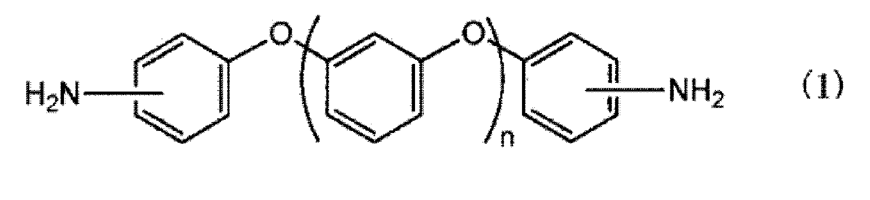
(式中、nは0又は1を表す。)
(b)4,4’-ジアミノジフェニルプロパン、3,4’-ジアミノジフェニルプロパン、4,4’-[1,3-フェニレンビス(1-メチリデン)]ビスアニリン、4,4’-[1,4-フェニレンビス(1-メチリデン)]ビスアニリン、p-フェニレンジアミン、m-フェニレンジアミン、クロル-p-フェニレンジアミン、4,4’-ジアミノジフェニルメタン、3,4’-ジアミノジフェニルメタン、2,4’-ジアミノジフェニルメタン、4,4’-ジアミノジフェニルスルフィド、3,4’-ジアミノジフェニルスルフィド、4,4’-ジアミノジフェニルスルフォン、3,4’-ジアミノジフェニルスルフォン、1,5-ジアミノナフタレン、3,3’-ジメチルベンジジン、3,3’,5,5’-テトラメチルベンジジン、3,3’-ジクロロベンジジン、2,2’-ジクロロベンジジン、3,3’,5,5’-テトラクロロベンジジン、2,4-ビス(β-アミノ-t-ブチル)トルエン、及びビス(p-β-アミノ-t-ブチルフェニル)エーテルからなる群より選ばれる1種以上の芳香族ジアミン、及び
(c)芳香族四塩基酸二無水物
を反応させて得られたポリアミック酸をイミド化して得られたものである高周波回路用基板。
(2)
上記銅箔の表面粗度Saが0.5μm以下である上記(1)記載の高周波回路用基板。
(3)
上記フッ素樹脂層を構成するフッ素樹脂がテトラフルオロエチレン・パーフルオロアルキルビニルエーテル共重合体(PFA)である上記(1)又は(2)記載の高周波用回路用基板。
(1)
(A)銅箔/(B)ポリイミド層/(C)フッ素樹脂層/(D)ポリイミド層/(E)銅箔がこの順に積層されている高周波回路用基板であって、
上記ポリイミド層を構成するポリイミド樹脂が、下記(a)~(c)成分:
(a)下記式(1)で表されるジアミン、
(b)4,4’-ジアミノジフェニルプロパン、3,4’-ジアミノジフェニルプロパン、4,4’-[1,3-フェニレンビス(1-メチリデン)]ビスアニリン、4,4’-[1,4-フェニレンビス(1-メチリデン)]ビスアニリン、p-フェニレンジアミン、m-フェニレンジアミン、クロル-p-フェニレンジアミン、4,4’-ジアミノジフェニルメタン、3,4’-ジアミノジフェニルメタン、2,4’-ジアミノジフェニルメタン、4,4’-ジアミノジフェニルスルフィド、3,4’-ジアミノジフェニルスルフィド、4,4’-ジアミノジフェニルスルフォン、3,4’-ジアミノジフェニルスルフォン、1,5-ジアミノナフタレン、3,3’-ジメチルベンジジン、3,3’,5,5’-テトラメチルベンジジン、3,3’-ジクロロベンジジン、2,2’-ジクロロベンジジン、3,3’,5,5’-テトラクロロベンジジン、2,4-ビス(β-アミノ-t-ブチル)トルエン、及びビス(p-β-アミノ-t-ブチルフェニル)エーテルからなる群より選ばれる1種以上の芳香族ジアミン、及び
(c)芳香族四塩基酸二無水物
を反応させて得られたポリアミック酸をイミド化して得られたものである高周波回路用基板。
(2)
上記銅箔の表面粗度Saが0.5μm以下である上記(1)記載の高周波回路用基板。
(3)
上記フッ素樹脂層を構成するフッ素樹脂がテトラフルオロエチレン・パーフルオロアルキルビニルエーテル共重合体(PFA)である上記(1)又は(2)記載の高周波用回路用基板。
本発明の高周波回路用基板は、高周波帯においても伝送損失が極めて少なく、さらに銅箔と樹脂層との接着性が高く、誘電特性及び耐吸湿性にも優れる。
本発明において用いられる銅箔としては、表面粗度Saが0.5μm以下の範囲内にあることが好ましく、0.2μm以下の範囲内にあることがより好ましい。表面粗度Saが0.5μmを超えると伝送損失が大きくなり、実用性能を満足しないことがある。銅箔の種類には電解箔と圧延箔とがあるが、どちらでも構わない。銅箔の厚さとしては、通常5~50μmであり、好ましくは8~40μmである。表面粗度は、従来、線状二次元における凹凸の算術平均であるRaが一般的に用いられてきたが、現実の表面が三次元的広がりを持っているため正確な値とは言い難い。これに対し、Saは三次元空間における凹凸の算術平均であり精度が高い。
銅箔表面は、無処理の銅箔表面であってもよく、また、該表面が金属メッキ処理、例えばニッケル、鉄、亜鉛、金、銀、アルミニウム、クロム、チタン、パラジウム、及び錫からなる群より選ばれる1種以上の金属でメッキ処理されていてもよい。また、無処理の銅箔表面又は金属メッキ処理された銅箔表面がシランカップリング剤等の薬剤で表面処理されたものであってもよい。好ましい金属メッキ処理としては、ニッケル、鉄、亜鉛、金、及びアルミニウムより選ばれる1種以上の金属による金属メッキ処理であり、より好ましくはニッケル又はアルミニウムによる金属メッキ処理である。また、場合により、ニッケル、鉄、亜鉛、金、及び錫からなる群より選ばれる1種以上の金属による金属メッキ処理が好ましい。
本発明において用いられるポリアミック酸は、下記式(1)で表されるジアミンと、特定の芳香族ジアミンと、芳香族四塩基酸二無水物とを反応させて得られる。
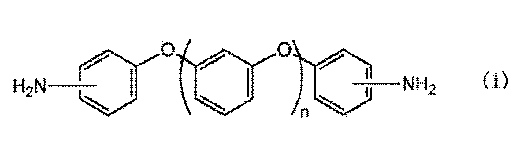
上記式(1)で表されるジアミンとしては、4,4’-ジアミノジフェニルエーテル、2,4’-ジアミノジフェニルエーテル、3,4’-ジアミノジフェニルエーテル等のジアミノジフェニルエーテル類;1,3-ビス(3-アミノフェノキシ)ベンゼン、1,3-ビス(4-アミノフェノキシ)ベンゼン等のビスアミノフェノキシベンゼン類;等が挙げられる。
上記式(1)で表されるジアミン以外の上記特定の芳香族ジアミンとしては、4,4’-ジアミノジフェニルプロパン、3,4’-ジアミノジフェニルプロパン等のジアミノジフェニルプロパン類;4,4’-[1,3-フェニレンビス(1-メチリデン)]ビスアニリン、4,4’-[1,4-フェニレンビス(1-メチリデン)]ビスアニリン等のビスアニリン類;p-フェニレンジアミン、m-フェニレンジアミン、クロル-p-フェニレンジアミン等のフェニレンジアミン類;4,4’-ジアミノジフェニルメタン、3,4’-ジアミノジフェニルメタン、2,4’-ジアミノジフェニルメタン等のジアミノジフェニルメタン類;4,4’-ジアミノジフェニルスルフィド、3,4’-ジアミノジフェニルスルフィド等のジアミノジフェニルスルフィド類;4,4’-ジアミノジフェニルスルフォン、3,4’-ジアミノジフェニルスルフォン等のジアミノジフェニルスルフォン類;1,5-ジアミノナフタレン等のジアミノナフタレン類;3,3’-ジメチルベンジジン、3,3’,5,5’-テトラメチルベンジジン、3,3’-ジクロロベンジジン、2,2’-ジクロロベンジジン、3,3’,5,5’-テトラクロロベンジジン等のベンジジン類;2,4-ビス(β-アミノ-t-ブチル)トルエン、ビス(p-β-アミノ-t-ブチルフェニル)エーテル;等を挙げることができる。これらの特定の芳香族ジアミンは単独で使用してもよく、2種以上を併用してもよい。
なお、上記特定の芳香族ジアミンは、ジアミン成分中で50モル%以上を占めることが好ましい。
なお、上記特定の芳香族ジアミンは、ジアミン成分中で50モル%以上を占めることが好ましい。
芳香族四塩基酸二無水物としては、芳香族環に4つのカルボキシ基が結合した構造の化合物の二無水物であれば特に制限はないが、例えば、ピロメリット酸二無水化物;2,3,6,7-ナフタレンテトラカルボン酸二無水化物、1,2,5,6-ナフタレンテトラカルボン酸二無水化物等のナフタレンテトラカルボン酸二無水化物;3,3’,4,4’-ビフェニルテトラカルボン酸二無水化物、2,2’,3,3’-ビフェニルテトラカルボン酸二無水化物等のビフェニルテトラカルボン酸二無水化物;2,3,4,5-チオフェンテトラカルボン酸二無水化物、2,2-ビス(3,4-ジカルボキシフェニル)プロパン酸二無水化物、ビス(3,4-ジカルボキシフェニル)スルフォン酸二無水化物、3,4,9,10-ペリレンテトラカルボン酸二無水化物;等を挙げることができ、ビフェニルテトラカルボン酸二無水化物が好ましい。これらの芳香族四塩基酸二無水物は単独で使用してもよく、2種以上を併用してもよい。
ポリアミック酸の固形分濃度を下げずにワニス粘度を下げるために、芳香族四塩基酸二無水物の一部を、同一又は異なる母核を有するジ(C1~C10)アルキルエステルとして用いてもよい。同一母核を有する芳香族四塩基酸のジ(C1~C10)アルキルエステルを得るには、ジメチルアミノエタノール等を触媒とし、芳香族四塩基酸二無水物とメタノール、エタノール、1-プロパノール等の所望するアルキル基に対応したアルコール類とを反応させればよい。また、芳香族四塩基酸を得るには、同様の触媒を用いて、芳香族四塩基酸二無水物と水とを反応させればよい。この際の触媒の使用量は、アルコール類又は水に対して1~10モル%程度であり、アルコール類又は水の使用量は、通常、芳香族四塩基酸二無水物の2.4~4.0倍モルである。反応温度は通常70~100℃であり、反応時間は通常2~5時間である。また、所定量の同一又は異なる母核を別途混合することもできる。芳香族四塩基酸二無水物と芳香族四塩基酸ジ(C1~C10)アルキルエステルとの使用割合は、モル比で前者が0.6~0.90に対して後者が通常0.10~0.4であることが好ましい。
本発明において、ジアミン成分の使用割合は、芳香族四塩基酸二無水物1モルに対して、あるいは芳香族四塩基酸二無水物と芳香族四塩基酸ジ(C1~C10)アルキルエステルとの合計モル数1モルに対して、アミン成分が通常0.95~1.05モル、好ましくは0.98~1.03モルである。この範囲を外れると、モル比のバランスがくずれたことに起因する特性の低下を招くことがある一方、粘度にも影響し、ハンドリングを困難にする場合がある。
本発明において用いられるポリアミック酸は、例えば以下のようにして調製することができる。
まず、芳香族四塩基酸二無水物とアルコール類とから上記のようにして溶剤中で芳香族四塩基酸ジアルキルエステルを調製する。次いで、この反応混合物を室温まで冷却後、窒素気流下、上記ジアミン成分を加え、70~80℃まで加熱して完全に溶解させる。次いで、55℃以下まで冷却し、そこに所定量の芳香族四塩基酸二無水物及び溶剤を加え、70~80℃まで加熱し、この温度で2~5時間反応させる。得られたポリアミック酸を含む溶液から溶媒を除去すれば、目的のポリアミック酸を得ることができる。なお、ポリアミック酸の濃度を下げて低粘度化する必要がない場合は、芳香族四塩基酸ジアルキルエステルの調製工程は必要なく、溶剤中で芳香族四塩基酸二無水物とジアミン成分とを上記に準じて反応させればよい。
まず、芳香族四塩基酸二無水物とアルコール類とから上記のようにして溶剤中で芳香族四塩基酸ジアルキルエステルを調製する。次いで、この反応混合物を室温まで冷却後、窒素気流下、上記ジアミン成分を加え、70~80℃まで加熱して完全に溶解させる。次いで、55℃以下まで冷却し、そこに所定量の芳香族四塩基酸二無水物及び溶剤を加え、70~80℃まで加熱し、この温度で2~5時間反応させる。得られたポリアミック酸を含む溶液から溶媒を除去すれば、目的のポリアミック酸を得ることができる。なお、ポリアミック酸の濃度を下げて低粘度化する必要がない場合は、芳香族四塩基酸ジアルキルエステルの調製工程は必要なく、溶剤中で芳香族四塩基酸二無水物とジアミン成分とを上記に準じて反応させればよい。
ポリアミック酸を調製する際の溶剤としては、N-メチル-2-ピロリドン、N,N-ジメチルアセトアミド、N,N-ジメチルホルムアミド、ジメチルスルホキシド、ジメチルスルホン、スルホラン、テトラメチレンスルホキシド、ジメチルイミダゾリジノン、ヘキサメチルホスホルアミド等の非プロトン性極性溶媒が適している。これらの溶剤は単独で使用してもよく、二種以上混合して使用してもよい。溶剤の使用量は、反応が進行する程度であれば特に制限はないが、ワニスとしての用途を考慮に入れると、下記のポリアミック酸組成物中の固形分濃度が通常2~50質量%程度となるように用いるのがよい。
本発明で用いられるポリアミック酸組成物は、ポリアミック酸と溶剤とを含有する。溶剤としては、上記溶剤を使用することができる。ポリアミック酸組成物は、種々の添加剤を加えることができる。添加剤としては、例えば、有機又は無機顔料;染料;レベリング剤;カブリ防止剤;退色防止剤;ハレーション防止剤;蛍光増白剤;界面活性剤;可塑剤;難燃剤;酸化防止剤;充填剤;静電防止剤;消泡剤;流動調整剤;γ-ブチロラクトンとピリジンとの組み合わせ、γ-バレロラクトンとピリジンとの組み合わせ等のイミド化触媒;安息香酸、m-ヒドロキシ安息香酸、p-ヒドロキシフェニル酢酸、p-ヒドロキシベンゼンスルホン酸、イソキノリン等のイミド化促進剤;トルエン、オルトジクロロベンゼン、ニトロベンゼン、無水酢酸/ピリジン等の(共沸)脱水剤;遅延剤;光安定剤;光触媒;防かび剤;抗菌剤;低誘電体;導電体;磁性体;層状鉱物;熱分解性化合物;等が挙げられる。特に、触媒(及びイミド化促進剤)や脱水剤を添加すれば、後のイミド化が促進され、比較的温和な条件でポリイミド層を得ることができる。
上記のポリアミック酸をイミド化して得られるポリイミド樹脂は、一般的なポリイミド樹脂と比較して誘電正接が低いため、誘電正接の低いフッ素樹脂と複合化することにより、回路基板を作成した場合に、10GHz以上の高周波数帯でも伝送損失を低く抑えることができる。ただし、フッ素樹脂は線膨張率が高いため、樹脂層全体の厚さに占めるフッ素樹脂層の厚さの割合は、10~90%が好ましい。なお、吸湿性や寸法安定性に着目すると、樹脂層全体の厚さに占めるフッ素樹脂層の厚さの割合は、55~90%が好ましく、60~85%がより好ましい。フッ素樹脂層の割合が低い場合、吸湿性や誘電特性が悪化する場合があり、また高すぎる場合は線膨張係数が高くなって寸法安定性が悪化する場合がある。
高周波回路用基板を製造するには、まず、2枚の単層銅張積層板を製造する。単層銅張積層板は、所望の膜厚、通常10~100μmになるように銅箔上に上記のポリアミック酸組成物を塗布し、50~150℃で5~180分間加熱して溶剤を乾燥させた後、窒素気流下、200~500℃で0.5~5時間熱処理してポリイミド層を形成することにより得ることができる。
上記により得られた2枚の単層銅張積層板のポリイミド層側にフッ素樹脂フィルムを挟んで熱圧着することにより、本発明の高周波回路用基板を得ることができる。フッ素樹脂フィルムの種類としては、本発明で用いられるポリイミド樹脂に対して高い接着性を有するものが好ましく、テトラフルオロエチレン・パーフルオロアルキルビニルエーテル共重合体(PFA)が特に好ましい。フッ素樹脂フィルムの表面は、接着性を高めるためにコロナ処理、プラズマ処理等が施されていてもよい。熱圧着は通常250~400℃の範囲内で、1~20分間、0.1~10MPaの圧力で行うことができる。熱圧着に際しては、フィルム間の空気の挟み込み等を防ぐために、真空プレス機を使用することが好ましい。
本発明の高周波回路用基板にスルーホールを形成する方法としては、ドリルによる加工法や、炭酸ガスレーザー、YAGレーザー、エキシマレーザー等のレーザーによる加工法を採用することができる。
また、本発明の高周波回路用基板のスルーホールにめっきを施す方法としては、従来周知の方法を採用することができる。例えば、無電解銅めっき及び電解銅めっきによるパターンめっき及び/又はパネルめっきを順次施せばよい。
本発明において高周波回路とは、単に高周波信号のみを伝送する回路からなるものだけでなく、高周波信号を低周波信号に変換して、生成された低周波信号を外部へ出力する伝送路や、高周波対応部品の駆動のために供給される電源を供給するための伝送路等、高周波信号ではない信号を伝送する伝送路も同一平面上に併設された回路も含まれる。
以下、実施例及び比較例に基づいて本発明をより具体的に説明するが、本発明は以下の実施例に限定されるものではない。
(銅箔の表面粗度及び凹凸間隔の測定方法)
レーザー顕微鏡(オリンパス株式会社製)を用い、銅箔の表面粗度(Sa)を測定した。
レーザー顕微鏡(オリンパス株式会社製)を用い、銅箔の表面粗度(Sa)を測定した。
(銅箔・ポリイミド層間の接着強度の測定方法)
JIS C5016-1994に準拠して、毎分50mmの速度で銅箔を銅箔除去面に対して90°の方向に引きはがしながら、引っ張り試験機により、銅箔の引きはがし強さを測定し、得られた値を接着強度とした。
JIS C5016-1994に準拠して、毎分50mmの速度で銅箔を銅箔除去面に対して90°の方向に引きはがしながら、引っ張り試験機により、銅箔の引きはがし強さを測定し、得られた値を接着強度とした。
(ポリイミド層間の接着強度の測定方法)
JIS C5016-1994に準拠して、毎分50mmの速度で銅箔を銅箔除去面に対して90°の方向に引きはがしながら、引っ張り試験機により、ポリイミド層間の引きはがし強さを測定し、得られた値を接着強度とした。
JIS C5016-1994に準拠して、毎分50mmの速度で銅箔を銅箔除去面に対して90°の方向に引きはがしながら、引っ張り試験機により、ポリイミド層間の引きはがし強さを測定し、得られた値を接着強度とした。
(誘電率、誘電正接の測定方法)
製造した高周波回路用基板の銅箔をエッチングした後、空洞共振器(関東電子応用開発株式会社製)により1GHzにて測定し、ネットワークアナライザー(アジレントテクノロジー株式会社製、型式8719ET)にて解析した。
製造した高周波回路用基板の銅箔をエッチングした後、空洞共振器(関東電子応用開発株式会社製)により1GHzにて測定し、ネットワークアナライザー(アジレントテクノロジー株式会社製、型式8719ET)にて解析した。
(伝送損失の測定方法)
エッチングにより、長さ10cmのマイクロストリップラインを作成し、ネットワークアナライザーを用いて20GHzにおける伝送損失を測定した。
エッチングにより、長さ10cmのマイクロストリップラインを作成し、ネットワークアナライザーを用いて20GHzにおける伝送損失を測定した。
(粘度の測定方法)
東機産業社製回転粘度計(TV-20形粘度計)により、25℃で測定した。
東機産業社製回転粘度計(TV-20形粘度計)により、25℃で測定した。
[合成例1]
乾燥窒素ガス導入管、冷却器、温度計、及び撹拌機を備えた三口フラスコにジメチルアセトアミド1326gを量りとり、30℃で、p-フェニレンジアミン81gと1,3-ビス(4-アミノフェノキシ)ベンゼン73gとを加え、いったん75℃まで加熱して溶解させた。その後55℃まで放冷し、3,3’,4,4’-ビフェニルテトラカルボン酸二無水物288gを加えて再び75℃まで加熱した。この温度で2時間加熱撹拌したのち、室温まで放冷した。窒素加圧下、ポリ(テトラフルオロエチレン)メンブラン(3μm)で濾過し、固形分濃度25質量%の赤褐色透明なワニス(ポリアミック酸組成物)1681g(収率95.1%)を得た。このワニスの25℃での粘度は、15300mPa・sであった。
乾燥窒素ガス導入管、冷却器、温度計、及び撹拌機を備えた三口フラスコにジメチルアセトアミド1326gを量りとり、30℃で、p-フェニレンジアミン81gと1,3-ビス(4-アミノフェノキシ)ベンゼン73gとを加え、いったん75℃まで加熱して溶解させた。その後55℃まで放冷し、3,3’,4,4’-ビフェニルテトラカルボン酸二無水物288gを加えて再び75℃まで加熱した。この温度で2時間加熱撹拌したのち、室温まで放冷した。窒素加圧下、ポリ(テトラフルオロエチレン)メンブラン(3μm)で濾過し、固形分濃度25質量%の赤褐色透明なワニス(ポリアミック酸組成物)1681g(収率95.1%)を得た。このワニスの25℃での粘度は、15300mPa・sであった。
[合成例2]
乾燥窒素ガス導入管、冷却器、温度計、及び撹拌機を備えた三口フラスコにジメチルアセトアミド1257gを量りとり、30℃で、p-フェニレンジアミン81gと3,4-ジアミノジフェニルエーテル50gとを加え、いったん75℃まで加熱して溶解させた。その後55℃まで放冷し、3,3’,4,4’-ビフェニルテトラカルボン酸二無水物288gを加えて再び75℃まで加熱した。この温度で2時間加熱撹拌したのち、室温まで放冷した。窒素加圧下、ポリ(テトラフルオロエチレン)メンブラン(3μm)で濾過し、固形分濃度25.0質量%の赤褐色透明なワニス(ポリアミック酸組成物)1609g(収率96.0%)を得た。このワニスの25℃での粘度は、17600mPa・sであった。
乾燥窒素ガス導入管、冷却器、温度計、及び撹拌機を備えた三口フラスコにジメチルアセトアミド1257gを量りとり、30℃で、p-フェニレンジアミン81gと3,4-ジアミノジフェニルエーテル50gとを加え、いったん75℃まで加熱して溶解させた。その後55℃まで放冷し、3,3’,4,4’-ビフェニルテトラカルボン酸二無水物288gを加えて再び75℃まで加熱した。この温度で2時間加熱撹拌したのち、室温まで放冷した。窒素加圧下、ポリ(テトラフルオロエチレン)メンブラン(3μm)で濾過し、固形分濃度25.0質量%の赤褐色透明なワニス(ポリアミック酸組成物)1609g(収率96.0%)を得た。このワニスの25℃での粘度は、17600mPa・sであった。
[合成例3(比較例)]
乾燥窒素ガス導入管、冷却器、温度計、及び撹拌機を備えた三口フラスコにジメチルアセトアミド1188gを量りとり、30℃で、p-フェニレンジアミン108gを加え、いったん75℃まで加熱して溶解させた。その後55℃まで放冷し、3,3’,4,4’-ビフェニルテトラカルボン酸二無水物288gを加えて再び75℃まで加熱した。この温度で2時間加熱撹拌したのち、室温まで放冷した。窒素加圧下、ポリ(テトラフルオロエチレン)メンブラン(3μm)で濾過し、固形分濃度25質量%の赤褐色透明なワニス(ポリアミック酸組成物)1511g(収率95.4%)を得た。このワニスの25℃での粘度は、15200mPa・sであった。
乾燥窒素ガス導入管、冷却器、温度計、及び撹拌機を備えた三口フラスコにジメチルアセトアミド1188gを量りとり、30℃で、p-フェニレンジアミン108gを加え、いったん75℃まで加熱して溶解させた。その後55℃まで放冷し、3,3’,4,4’-ビフェニルテトラカルボン酸二無水物288gを加えて再び75℃まで加熱した。この温度で2時間加熱撹拌したのち、室温まで放冷した。窒素加圧下、ポリ(テトラフルオロエチレン)メンブラン(3μm)で濾過し、固形分濃度25質量%の赤褐色透明なワニス(ポリアミック酸組成物)1511g(収率95.4%)を得た。このワニスの25℃での粘度は、15200mPa・sであった。
[製造例1~2、製造比較例1]
合成例1~3で得られたポリアミック酸組成物を、乾燥後の膜厚が25μmになるように、厚さが12μm、表面粗度Saが0.11μmである電解銅箔の片面に塗布し、乾燥させた。その後、窒素気流下200~350℃で加熱処理し、ポリアミック酸のイミド化反応を行い、単層銅張積層板を製造した。銅箔とポリイミド層との間の引きはがし強さを測定したところ、表1のような結果となった。
合成例1~3で得られたポリアミック酸組成物を、乾燥後の膜厚が25μmになるように、厚さが12μm、表面粗度Saが0.11μmである電解銅箔の片面に塗布し、乾燥させた。その後、窒素気流下200~350℃で加熱処理し、ポリアミック酸のイミド化反応を行い、単層銅張積層板を製造した。銅箔とポリイミド層との間の引きはがし強さを測定したところ、表1のような結果となった。

[実施例1~2]
製造例1で得られた単層銅張積層板2枚のポリイミド層間に厚さ25μmのテトラフルオロエチレン・パーフルオロアルキルビニルエーテル共重合体(PFA)フィルム(ダイキン株式会社製、製品名AF-0025)を挟み、真空プレス機を用いて320℃で10分間熱プレスすることにより、本発明の高周波回路用基板(基板1)を製造した。また、製造例2で得られた単層銅張積層板2枚を用いるほかは上記と同様にして、本発明の高周波回路用基板(基板2)を製造した。
製造例1で得られた単層銅張積層板2枚のポリイミド層間に厚さ25μmのテトラフルオロエチレン・パーフルオロアルキルビニルエーテル共重合体(PFA)フィルム(ダイキン株式会社製、製品名AF-0025)を挟み、真空プレス機を用いて320℃で10分間熱プレスすることにより、本発明の高周波回路用基板(基板1)を製造した。また、製造例2で得られた単層銅張積層板2枚を用いるほかは上記と同様にして、本発明の高周波回路用基板(基板2)を製造した。
[比較例1~2]
製造例1で得られた単層銅張積層板を2枚用意し、一方のポリイミド面にエポキシ樹脂系接着ワニスPHY-3E(日本化薬株式会社製)を乾燥後の膜厚が25μmになるように塗布・乾燥し、他方の単層銅張積層板のポリイミド面をあてがって170℃、3MPaで1時間熱プレスすることにより、比較用基板(基板3)を製造した。また、製造例2で得られた単層銅張積層板2枚を用いるほかは上記と同様にして、比較用基板(基板4)を製造した。
製造例1で得られた単層銅張積層板を2枚用意し、一方のポリイミド面にエポキシ樹脂系接着ワニスPHY-3E(日本化薬株式会社製)を乾燥後の膜厚が25μmになるように塗布・乾燥し、他方の単層銅張積層板のポリイミド面をあてがって170℃、3MPaで1時間熱プレスすることにより、比較用基板(基板3)を製造した。また、製造例2で得られた単層銅張積層板2枚を用いるほかは上記と同様にして、比較用基板(基板4)を製造した。
上記基板1~4を用い、20GHzでの伝送損失を測定した。また、ポリイミド層間の引きはがし強さを測定した。また、260℃の半田浴に1分間浮かべ、基板表面の外観異状の有無を観察した。さらに、銅箔をエッチングし、1GHzにおける樹脂層の誘電率、誘電正接を測定した。結果を表2に示す。

[合成例4]
乾燥窒素ガス導入管、冷却器、温度計、及び撹拌機を備えた三口フラスコに3,3’,4,4’-ビフェニルテトラカルボン酸二無水物23.52g、メタノール6.14g、ジメチルアミノエタノール1.2g、及びジメチルアセトアミド1266gを量りとり、70~75℃で2時間加熱撹拌した。反応後、放冷し、30℃になったらp-フェニレンジアミン86.4gと1,3-ビス(4-アミノフェノキシ)ベンゼン58.4gとを加え、いったん75℃まで加熱して溶解させた。その後55℃まで放冷し、3,3’,4,4’-ビフェニルテトラカルボン酸二無水物270.48gを加えて再び75℃まで加熱した。この温度で2時間加熱撹拌したのち、室温まで放冷した。窒素加圧下、ポリ(テトラフルオロエチレン)メンブラン(3μm)で濾過し、固形分濃度26.0質量%の赤褐色透明なワニス(ポリアミック酸組成物)1625.45g(収率95.0%)を得た。このワニスの25℃での粘度は、11200mPa・sであった。
乾燥窒素ガス導入管、冷却器、温度計、及び撹拌機を備えた三口フラスコに3,3’,4,4’-ビフェニルテトラカルボン酸二無水物23.52g、メタノール6.14g、ジメチルアミノエタノール1.2g、及びジメチルアセトアミド1266gを量りとり、70~75℃で2時間加熱撹拌した。反応後、放冷し、30℃になったらp-フェニレンジアミン86.4gと1,3-ビス(4-アミノフェノキシ)ベンゼン58.4gとを加え、いったん75℃まで加熱して溶解させた。その後55℃まで放冷し、3,3’,4,4’-ビフェニルテトラカルボン酸二無水物270.48gを加えて再び75℃まで加熱した。この温度で2時間加熱撹拌したのち、室温まで放冷した。窒素加圧下、ポリ(テトラフルオロエチレン)メンブラン(3μm)で濾過し、固形分濃度26.0質量%の赤褐色透明なワニス(ポリアミック酸組成物)1625.45g(収率95.0%)を得た。このワニスの25℃での粘度は、11200mPa・sであった。
[実施例3]
合成例4で得られたポリアミック酸組成物を、乾燥後の膜厚が25μmになるように、厚さ18μmの表面粗化処理の全くなされていない圧延銅箔(Sa=0.143μm)の片面に塗布して乾燥させた。その後、窒素気流下200~350℃で加熱処理し、ポリアミック酸のイミド化反応を行い、単層銅張積層板を製造した。
得られた単層銅張積層板2枚のポリイミド層間に厚さ25μmのテトラフルオロエチレン・パーフルオロアルキルビニルエーテル共重合体(PFA)フィルム(ダイキン株式会社製、製品名AF-0025)を挟み、真空プレス機を用いて320℃で10分間熱プレスすることにより、本発明の高周波回路用基板(基板5)を製造した。
合成例4で得られたポリアミック酸組成物を、乾燥後の膜厚が25μmになるように、厚さ18μmの表面粗化処理の全くなされていない圧延銅箔(Sa=0.143μm)の片面に塗布して乾燥させた。その後、窒素気流下200~350℃で加熱処理し、ポリアミック酸のイミド化反応を行い、単層銅張積層板を製造した。
得られた単層銅張積層板2枚のポリイミド層間に厚さ25μmのテトラフルオロエチレン・パーフルオロアルキルビニルエーテル共重合体(PFA)フィルム(ダイキン株式会社製、製品名AF-0025)を挟み、真空プレス機を用いて320℃で10分間熱プレスすることにより、本発明の高周波回路用基板(基板5)を製造した。
[比較例3]
実施例3で得られた単層銅張積層板を2枚用意し、一方のポリイミド面にエポキシ樹脂系接着ワニスPHY-3E(日本化薬株式会社製)を乾燥後の膜厚が25μmになるように塗布・乾燥し、他方の単層銅張積層板のポリイミド面をあてがって170℃、3MPaで1時間熱プレスすることにより、比較用基板(基板6)を製造した。
実施例3で得られた単層銅張積層板を2枚用意し、一方のポリイミド面にエポキシ樹脂系接着ワニスPHY-3E(日本化薬株式会社製)を乾燥後の膜厚が25μmになるように塗布・乾燥し、他方の単層銅張積層板のポリイミド面をあてがって170℃、3MPaで1時間熱プレスすることにより、比較用基板(基板6)を製造した。
上記基板5、6を用い、20GHzでの伝送損失を測定した。また、銅箔とポリイミド層との間の引きはがし強さ、及びポリイミド層間の引きはがし強さを測定した。また、260℃の半田浴に1分間浮かべ、基板表面の外観異状の有無を観察した。さらに、銅箔をエッチングし、1GHzにおける樹脂層の誘電率、誘電正接を測定した。結果を表3に示す。

[実施例4、5]
合成例1、2で得られたポリアミック酸組成物を、乾燥後の膜厚が12.5μmになるように、厚さが12μm、表面粗度Saが0.11μmである電解銅箔の片面に塗布し、乾燥させた。その後、窒素気流下200~350℃で加熱処理し、ポリアミック酸のイミド化反応を行い、単層銅張積層板を製造した。
得られた単層銅張積層板2枚のポリイミド層間に厚さ50μmのテトラフルオロエチレン・パーフルオロアルキルビニルエーテル共重合体(PFA)フィルム(ダイキン株式会社製、製品名AF-0050)を挟み、真空プレス機を用いて320℃で10分間熱プレスすることにより、本発明の高周波回路用基板(基板7、8)を製造した。
合成例1、2で得られたポリアミック酸組成物を、乾燥後の膜厚が12.5μmになるように、厚さが12μm、表面粗度Saが0.11μmである電解銅箔の片面に塗布し、乾燥させた。その後、窒素気流下200~350℃で加熱処理し、ポリアミック酸のイミド化反応を行い、単層銅張積層板を製造した。
得られた単層銅張積層板2枚のポリイミド層間に厚さ50μmのテトラフルオロエチレン・パーフルオロアルキルビニルエーテル共重合体(PFA)フィルム(ダイキン株式会社製、製品名AF-0050)を挟み、真空プレス機を用いて320℃で10分間熱プレスすることにより、本発明の高周波回路用基板(基板7、8)を製造した。
上記基板7、8を用い、20GHzでの伝送損失を測定した。また、ポリイミド層間の引きはがし強さを測定した。また、片面の銅箔をエッチングにより全て除去し、沸騰水中に2時間放置した後、260℃の半田浴に1分間浮かべ、基板表面の外観異常の有無を観察した(吸湿耐半田リフロー)。さらに、銅箔を全面エッチングし、1GHzにおける樹脂層の誘電率、誘電正接を測定した。結果を表4に示す。

本発明によれば、伝送損失が少なく、接着性、耐半田リフロー性に優れた高周波回路用基板が得られる。この高周波回路基板は、高速伝送用の各種高周波回路用基板として有用である。
Claims (3)
- (A)銅箔/(B)ポリイミド層/(C)フッ素樹脂層/(D)ポリイミド層/(E)銅箔がこの順に積層されている高周波回路用基板であって、
前記ポリイミド層を構成するポリイミド樹脂が、下記(a)~(c)成分:
(a)下記式(1)で表されるジアミン、

(式中、nは0又は1を表す。)
(b)4,4’-ジアミノジフェニルプロパン、3,4’-ジアミノジフェニルプロパン、4,4’-[1,3-フェニレンビス(1-メチリデン)]ビスアニリン、4,4’-[1,4-フェニレンビス(1-メチリデン)]ビスアニリン、p-フェニレンジアミン、m-フェニレンジアミン、クロル-p-フェニレンジアミン、4,4’-ジアミノジフェニルメタン、3,4’-ジアミノジフェニルメタン、2,4’-ジアミノジフェニルメタン、4,4’-ジアミノジフェニルスルフィド、3,4’-ジアミノジフェニルスルフィド、4,4’-ジアミノジフェニルスルフォン、3,4’-ジアミノジフェニルスルフォン、1,5-ジアミノナフタレン、3,3’-ジメチルベンジジン、3,3’,5,5’-テトラメチルベンジジン、3,3’-ジクロロベンジジン、2,2’-ジクロロベンジジン、3,3’,5,5’-テトラクロロベンジジン、2,4-ビス(β-アミノ-t-ブチル)トルエン、及びビス(p-β-アミノ-t-ブチルフェニル)エーテルからなる群より選ばれる1種以上の芳香族ジアミン、及び
(c)芳香族四塩基酸二無水物
を反応させて得られたポリアミック酸をイミド化して得られたものである高周波回路用基板。 - 前記銅箔の表面粗度Saが0.5μm以下である請求項1記載の高周波回路用基板。
- 前記フッ素樹脂層を構成するフッ素樹脂がテトラフルオロエチレン・パーフルオロアルキルビニルエーテル共重合体(PFA)である請求項1又は2記載の高周波回路用基板。
Applications Claiming Priority (4)
| Application Number | Priority Date | Filing Date | Title |
|---|---|---|---|
| JP2013-000326 | 2013-01-07 | ||
| JP2013000326 | 2013-01-07 | ||
| JP2013-127443 | 2013-06-18 | ||
| JP2013127443 | 2013-06-18 |
Publications (1)
| Publication Number | Publication Date |
|---|---|
| WO2014106930A1 true WO2014106930A1 (ja) | 2014-07-10 |
Family
ID=51062252
Family Applications (1)
| Application Number | Title | Priority Date | Filing Date |
|---|---|---|---|
| PCT/JP2013/084122 Ceased WO2014106930A1 (ja) | 2013-01-07 | 2013-12-19 | 高周波回路用基板 |
Country Status (2)
| Country | Link |
|---|---|
| TW (1) | TW201431679A (ja) |
| WO (1) | WO2014106930A1 (ja) |
Cited By (2)
| Publication number | Priority date | Publication date | Assignee | Title |
|---|---|---|---|---|
| CN113677532A (zh) * | 2019-04-16 | 2021-11-19 | Agc株式会社 | 层叠体、印刷基板的制造方法、印刷基板及天线 |
| CN114126202A (zh) * | 2020-08-29 | 2022-03-01 | 华为技术有限公司 | 一种覆铜基板及其制备方法、电路板、电子设备 |
Families Citing this family (1)
| Publication number | Priority date | Publication date | Assignee | Title |
|---|---|---|---|---|
| KR102353961B1 (ko) * | 2016-07-22 | 2022-01-21 | 에이지씨 가부시키가이샤 | 액상 조성물, 그리고 그 액상 조성물을 사용한, 필름 및 적층체의 제조 방법 |
Citations (2)
| Publication number | Priority date | Publication date | Assignee | Title |
|---|---|---|---|---|
| JP2005146074A (ja) * | 2003-11-13 | 2005-06-09 | Nippon Kayaku Co Ltd | ポリアミド酸、ポリアミド組成物及びポリイミド |
| JP2011051203A (ja) * | 2009-09-01 | 2011-03-17 | Toyobo Co Ltd | 多層ポリイミドフィルムおよびプリント配線板 |
-
2013
- 2013-12-19 WO PCT/JP2013/084122 patent/WO2014106930A1/ja not_active Ceased
-
2014
- 2014-01-02 TW TW103100067A patent/TW201431679A/zh unknown
Patent Citations (2)
| Publication number | Priority date | Publication date | Assignee | Title |
|---|---|---|---|---|
| JP2005146074A (ja) * | 2003-11-13 | 2005-06-09 | Nippon Kayaku Co Ltd | ポリアミド酸、ポリアミド組成物及びポリイミド |
| JP2011051203A (ja) * | 2009-09-01 | 2011-03-17 | Toyobo Co Ltd | 多層ポリイミドフィルムおよびプリント配線板 |
Cited By (2)
| Publication number | Priority date | Publication date | Assignee | Title |
|---|---|---|---|---|
| CN113677532A (zh) * | 2019-04-16 | 2021-11-19 | Agc株式会社 | 层叠体、印刷基板的制造方法、印刷基板及天线 |
| CN114126202A (zh) * | 2020-08-29 | 2022-03-01 | 华为技术有限公司 | 一种覆铜基板及其制备方法、电路板、电子设备 |
Also Published As
| Publication number | Publication date |
|---|---|
| TW201431679A (zh) | 2014-08-16 |
Similar Documents
| Publication | Publication Date | Title |
|---|---|---|
| JP7429519B2 (ja) | 多層ポリイミドフィルム | |
| JP6403460B2 (ja) | 金属張積層体、回路基板及びポリイミド | |
| JP7122162B2 (ja) | 熱可塑性ポリイミドフィルム、多層ポリイミドフィルム、およびフレキシブル金属張積層板 | |
| JP4634439B2 (ja) | 金属積層板及びその製造方法 | |
| JP2017165909A (ja) | ポリイミド、樹脂フィルム及び金属張積層板 | |
| US12351684B2 (en) | Polyimide resin precursor, polyimide resin, metal-clad laminated board, laminate, and flexible printed wiring board | |
| TW201702069A (zh) | 包含聚醯亞胺樹脂之金屬積層板及其製造方法 | |
| WO2016052316A1 (ja) | ポリアミド酸、ポリイミド、樹脂フィルム及び金属張積層板 | |
| JP2015106629A (ja) | 高周波回路用プリント配線基板 | |
| JP2011143678A (ja) | 多層ポリイミドフィルム及びそれを用いたフレキシブル金属張積層板 | |
| JP2015193117A (ja) | 金属張積層体及び回路基板 | |
| JP2014045076A (ja) | 高周波回路用基板 | |
| KR20140081143A (ko) | 다층 연성금속박 적층체 및 이의 제조방법 | |
| JP7696740B2 (ja) | 樹脂フィルム、その製造方法、金属張積層板及び回路基板 | |
| JP2014138020A (ja) | 高周波回路用プリント配線基板 | |
| CN107428146A (zh) | 聚酰亚胺层叠膜、聚酰亚胺层叠膜的制造方法、热塑性聚酰亚胺的制造方法、以及柔性金属包覆层叠体的制造方法 | |
| KR101195719B1 (ko) | 접착 필름 및 이것으로부터 얻어지는 치수 안정성을 향상시킨 연성 금속장 적층판, 및 그의 제조 방법 | |
| TW201431679A (zh) | 高頻電路用基板 | |
| JP2008135759A (ja) | ポリイミドベンゾオキサゾールフィルムを絶縁層として用いたプリント配線基板用ベース基板、多層プリント配線板 | |
| JP2014022474A (ja) | 高周波回路用基板 | |
| JP4326887B2 (ja) | 配線基板用積層体 | |
| JP4412708B2 (ja) | ポリアミド酸、ポリアミド組成物及びポリイミド | |
| JP4936729B2 (ja) | フレキシブルプリント配線板用基板及びその製造方法 | |
| JP4694142B2 (ja) | フレキシブルプリント配線板用基板の製造方法 | |
| JP2019093548A (ja) | 長尺ポリイミド積層体およびその製造方法 |
Legal Events
| Date | Code | Title | Description |
|---|---|---|---|
| 121 | Ep: the epo has been informed by wipo that ep was designated in this application |
Ref document number: 13870354 Country of ref document: EP Kind code of ref document: A1 |
|
| NENP | Non-entry into the national phase |
Ref country code: DE |
|
| NENP | Non-entry into the national phase |
Ref country code: JP |
|
| 122 | Ep: pct application non-entry in european phase |
Ref document number: 13870354 Country of ref document: EP Kind code of ref document: A1 |