WO2014104858A1 - 투명표시장치 및 그 제어 방법 - Google Patents
투명표시장치 및 그 제어 방법 Download PDFInfo
- Publication number
- WO2014104858A1 WO2014104858A1 PCT/KR2013/012398 KR2013012398W WO2014104858A1 WO 2014104858 A1 WO2014104858 A1 WO 2014104858A1 KR 2013012398 W KR2013012398 W KR 2013012398W WO 2014104858 A1 WO2014104858 A1 WO 2014104858A1
- Authority
- WO
- WIPO (PCT)
- Prior art keywords
- transparent display
- image
- light
- display device
- control unit
- Prior art date
Links
Images


Classifications
-
- G—PHYSICS
- G09—EDUCATION; CRYPTOGRAPHY; DISPLAY; ADVERTISING; SEALS
- G09G—ARRANGEMENTS OR CIRCUITS FOR CONTROL OF INDICATING DEVICES USING STATIC MEANS TO PRESENT VARIABLE INFORMATION
- G09G3/00—Control arrangements or circuits, of interest only in connection with visual indicators other than cathode-ray tubes
- G09G3/20—Control arrangements or circuits, of interest only in connection with visual indicators other than cathode-ray tubes for presentation of an assembly of a number of characters, e.g. a page, by composing the assembly by combination of individual elements arranged in a matrix no fixed position being assigned to or needed to be assigned to the individual characters or partial characters
- G09G3/2003—Display of colours
-
- G—PHYSICS
- G09—EDUCATION; CRYPTOGRAPHY; DISPLAY; ADVERTISING; SEALS
- G09G—ARRANGEMENTS OR CIRCUITS FOR CONTROL OF INDICATING DEVICES USING STATIC MEANS TO PRESENT VARIABLE INFORMATION
- G09G3/00—Control arrangements or circuits, of interest only in connection with visual indicators other than cathode-ray tubes
- G09G3/20—Control arrangements or circuits, of interest only in connection with visual indicators other than cathode-ray tubes for presentation of an assembly of a number of characters, e.g. a page, by composing the assembly by combination of individual elements arranged in a matrix no fixed position being assigned to or needed to be assigned to the individual characters or partial characters
- G09G3/22—Control arrangements or circuits, of interest only in connection with visual indicators other than cathode-ray tubes for presentation of an assembly of a number of characters, e.g. a page, by composing the assembly by combination of individual elements arranged in a matrix no fixed position being assigned to or needed to be assigned to the individual characters or partial characters using controlled light sources
- G09G3/30—Control arrangements or circuits, of interest only in connection with visual indicators other than cathode-ray tubes for presentation of an assembly of a number of characters, e.g. a page, by composing the assembly by combination of individual elements arranged in a matrix no fixed position being assigned to or needed to be assigned to the individual characters or partial characters using controlled light sources using electroluminescent panels
- G09G3/32—Control arrangements or circuits, of interest only in connection with visual indicators other than cathode-ray tubes for presentation of an assembly of a number of characters, e.g. a page, by composing the assembly by combination of individual elements arranged in a matrix no fixed position being assigned to or needed to be assigned to the individual characters or partial characters using controlled light sources using electroluminescent panels semiconductive, e.g. using light-emitting diodes [LED]
- G09G3/3208—Control arrangements or circuits, of interest only in connection with visual indicators other than cathode-ray tubes for presentation of an assembly of a number of characters, e.g. a page, by composing the assembly by combination of individual elements arranged in a matrix no fixed position being assigned to or needed to be assigned to the individual characters or partial characters using controlled light sources using electroluminescent panels semiconductive, e.g. using light-emitting diodes [LED] organic, e.g. using organic light-emitting diodes [OLED]
-
- H—ELECTRICITY
- H10—SEMICONDUCTOR DEVICES; ELECTRIC SOLID-STATE DEVICES NOT OTHERWISE PROVIDED FOR
- H10K—ORGANIC ELECTRIC SOLID-STATE DEVICES
- H10K59/00—Integrated devices, or assemblies of multiple devices, comprising at least one organic light-emitting element covered by group H10K50/00
- H10K59/50—OLEDs integrated with light modulating elements, e.g. with electrochromic elements, photochromic elements or liquid crystal elements
-
- G—PHYSICS
- G09—EDUCATION; CRYPTOGRAPHY; DISPLAY; ADVERTISING; SEALS
- G09G—ARRANGEMENTS OR CIRCUITS FOR CONTROL OF INDICATING DEVICES USING STATIC MEANS TO PRESENT VARIABLE INFORMATION
- G09G2320/00—Control of display operating conditions
- G09G2320/02—Improving the quality of display appearance
- G09G2320/0242—Compensation of deficiencies in the appearance of colours
-
- G—PHYSICS
- G09—EDUCATION; CRYPTOGRAPHY; DISPLAY; ADVERTISING; SEALS
- G09G—ARRANGEMENTS OR CIRCUITS FOR CONTROL OF INDICATING DEVICES USING STATIC MEANS TO PRESENT VARIABLE INFORMATION
- G09G2320/00—Control of display operating conditions
- G09G2320/06—Adjustment of display parameters
- G09G2320/0626—Adjustment of display parameters for control of overall brightness
-
- G—PHYSICS
- G09—EDUCATION; CRYPTOGRAPHY; DISPLAY; ADVERTISING; SEALS
- G09G—ARRANGEMENTS OR CIRCUITS FOR CONTROL OF INDICATING DEVICES USING STATIC MEANS TO PRESENT VARIABLE INFORMATION
- G09G2320/00—Control of display operating conditions
- G09G2320/06—Adjustment of display parameters
- G09G2320/066—Adjustment of display parameters for control of contrast
-
- G—PHYSICS
- G09—EDUCATION; CRYPTOGRAPHY; DISPLAY; ADVERTISING; SEALS
- G09G—ARRANGEMENTS OR CIRCUITS FOR CONTROL OF INDICATING DEVICES USING STATIC MEANS TO PRESENT VARIABLE INFORMATION
- G09G2320/00—Control of display operating conditions
- G09G2320/06—Adjustment of display parameters
- G09G2320/0673—Adjustment of display parameters for control of gamma adjustment, e.g. selecting another gamma curve
-
- G—PHYSICS
- G09—EDUCATION; CRYPTOGRAPHY; DISPLAY; ADVERTISING; SEALS
- G09G—ARRANGEMENTS OR CIRCUITS FOR CONTROL OF INDICATING DEVICES USING STATIC MEANS TO PRESENT VARIABLE INFORMATION
- G09G2360/00—Aspects of the architecture of display systems
- G09G2360/14—Detecting light within display terminals, e.g. using a single or a plurality of photosensors
- G09G2360/144—Detecting light within display terminals, e.g. using a single or a plurality of photosensors the light being ambient light
-
- G—PHYSICS
- G09—EDUCATION; CRYPTOGRAPHY; DISPLAY; ADVERTISING; SEALS
- G09G—ARRANGEMENTS OR CIRCUITS FOR CONTROL OF INDICATING DEVICES USING STATIC MEANS TO PRESENT VARIABLE INFORMATION
- G09G2360/00—Aspects of the architecture of display systems
- G09G2360/14—Detecting light within display terminals, e.g. using a single or a plurality of photosensors
- G09G2360/145—Detecting light within display terminals, e.g. using a single or a plurality of photosensors the light originating from the display screen
Definitions
- the present invention relates to a transparent display device and a control method thereof, and more particularly, to a transparent display device and a control method of improving visibility by minimizing optical interference to an image displayed by the transparent display device.
- the transparent display device is a display device in which the background of the screen is visible.
- the transparent display device is mainly implemented by projecting onto a non-emission liquid crystal panel.
- the liquid crystal display (LCD) has excellent light shielding rate but uses two polarizing plates, and thus has low transmittance, making it difficult to use as a transparent display device.
- the transparent display device is mainly implemented in an organic light emitting display (OLED) capable of self-emission.
- OLED organic light emitting display
- the transparent display device may be applied to a windshield or a home glass of a vehicle to provide a user with information of a display device and surrounding environment information at the same time.
- the transparent display device transmits light incident on the rear surface of the transparent display device to the eye as it is, based on light transmittance.
- the light incident on the rear surface is transmitted to the eye as it is, so that the object on the rear side can be recognized.
- the inventors of the present invention recognize that when color noise is incident on the rear surface of the transparent display device, it may be difficult to recognize the information because the color of the portion where the information of the transparent display device is displayed and the portion where the information is not is distorted or the color difference is reduced.
- the rear of the transparent display device is bright, the difference in brightness between the portion where the information of the transparent display device is displayed and the portion that is not is reduced, so that it may be difficult to recognize the information.
- the visibility of the displayed image is inferior.
- the inventors of the present invention have recognized that when color noise is incident from the rear surface of the transparent display device, it is necessary to secure the visibility of the image by correcting the brightness of the transparent display device.
- an object of the present invention is to provide a transparent display device and a transparent display device control method for improving the visibility of an image displayed on the transparent display device and implementing a high quality display.
- Another object of the present invention is to provide a transparent display device and a transparent display device control method having improved power consumption, product life and reliability through image correction and panel driving control.
- Another object of the present invention is to provide a transparent display device and a method for controlling the transparent display device, in which color noise incident on the rear surface of the transparent display device is reduced.
- Another object of the present invention is to provide a transparent display device and a method for controlling the transparent display device that can be actively or passively applied to an external environment and provide an optimal image quality according to a change in the external environment.
- the transparent display device includes a transparent display unit.
- the transparent display unit includes a plurality of pixels configured to display an image and a plurality of transmission units disposed adjacent to the plurality of pixels.
- the transparent display device includes at least one light sensor and a light control unit. At least one optical sensor measures an optical characteristic incident on a rear surface of the transparent display unit.
- the light control unit controls the amount of light incident on the rear surface of the transparent display unit and transmitted through the plurality of transmission units.
- the transparent display device includes a control unit, and the control unit corrects the transmittance of the light control unit and the image of the transparent display unit based on the optical characteristics.
- the transparent display device can be actively or passively applied to the external environment, and can provide the optimum image quality according to the change of the external environment.
- the transparent display device includes a transparent display unit including a plurality of pixels configured to display an image and a plurality of transmission units disposed adjacent to the plurality of pixels.
- the transparent display device includes at least one optical sensor configured to measure color information of external light incident on the rear surface of the transparent display unit.
- the transparent display device includes a controller configured to correct an image of the transparent display based on color information. In the transparent display device, power consumption, product lifespan, and reliability may be improved through image correction and panel driving control. In addition, color noise incident on the rear surface of the transparent display device may be reduced.
- FIG. 1 is a block diagram of a transparent display device according to an embodiment of the present invention.
- FIG. 2 is a schematic cross-sectional view of a transparent display device according to an exemplary embodiment of the present invention.
- FIG. 3 is a block diagram illustrating driving of a transparent display device according to an exemplary embodiment of the present invention.
- FIG. 4 is a block diagram of a system of a transparent display device according to an embodiment of the present invention.
- 5 and 6 are schematic cross-sectional views of pixels of a transparent display device according to an exemplary embodiment of the present invention.
- FIG. 7 is a schematic diagram illustrating a gamma curve of an image displayed by a transparent display device according to an exemplary embodiment.
- FIG. 8 is a schematic diagram of a transparent display device according to an embodiment of the present invention.
- FIG. 9 is a plan view of a transparent display device according to an exemplary embodiment of the present invention.
- FIG. 10 is a flowchart illustrating a control method of a transparent display device according to an embodiment of the present invention.
- 11A is a schematic cross-sectional view of a transparent display device according to an embodiment of the present invention.
- 11B and 11C are schematic diagrams of light incident to a transparent display device according to an exemplary embodiment of the present invention.
- FIG. 12 is a schematic diagram of a light controller of a transparent display device according to an exemplary embodiment of the present invention.
- FIG. 13 is a schematic diagram of a transparent display device according to an embodiment of the present invention.
- FIG. 14 is a block diagram of a transparent display device according to an embodiment of the present invention.
- 15 is a conceptual diagram of a gamma curve in a transparent display device according to an embodiment of the present invention.
- 16A, 16B, and 16C are conceptual views of a display image in a transparent display device according to an embodiment of the present invention.
- 17 is a conceptual diagram of a histogram analysis of an image according to an embodiment of the present invention.
- FIG. 18 is a block diagram of a light transmittance control apparatus according to an embodiment of the present invention.
- 19A and 19B are conceptual views illustrating spot correction in the light control unit of the transparent display device according to the exemplary embodiment.
- FIG. 20 is a flowchart illustrating a control method of a transparent display device according to an embodiment of the present invention.
- references to elements or layers "on" other elements or layers include all instances where another layer or other element is directly over or in the middle of another element.
- first, second, etc. are used to describe various components, these components are of course not limited by these terms. These terms are only used to distinguish one component from another. Therefore, of course, the first component mentioned below may be a second component within the technical spirit of the present invention.
- an image refers to a visual image and means all elements appearing on a screen or a display device.
- the image may include a moving image, a still image, a still cut, and the like, and, in the case of a moving image, may include a plurality of frames, and each of the frames may include a plurality of layers or regions.
- the image may be a 2D image or a 3D image.
- both the two-dimensional image and the three-dimensional image is referred to as an image.
- an image signal means that an image is converted into an electrical signal and output so as to be displayed on a screen of a screen or a panel of a display device, and means a signal for transmitting and receiving image data.
- image processing or image correction means processing an input image through a processing unit or a processor and processing the image according to the purpose, and includes both analog signal processing and digital signal processing.
- image processing means digital image processing on an image, but may be broadly interpreted without being limited thereto.
- the image processing in the present specification may include at least four types of point processing, region processing, geometric processing, and frame processing. Point processing is performed pixel by pixel based on the position of the pixel.
- the region processing may change the pixel value based on the original value of the pixel and the value of the neighboring pixel, and the geometric processing may change the position or arrangement of the pixels.
- the frame processing may change pixel values based on operations on two or more images.
- the transparent display device refers to a display device in which at least some regions of the screen of the display device visually recognized by the user are transparent.
- the transparency of the transparent display device refers to a transparent display device at which a user can recognize at least an object behind the display device.
- the transparent display device means, for example, a display device having a transparent display device transmittance of at least 20% or more. The amount of light incident and transmitted through the rear surface of the transparent display device may be determined according to the transmittance of the transparent display device.
- the contrast ratio in the transparent display device depends on the ambient illumination environment, and especially on the light incident to the rear surface.
- Table 1 is a table showing white / black luminance and contrast ratios of a display device reflecting 1.5% of light incident to the front side and a transparent display device passing 20% of light incident to the rear side under a 200 lux and 2000 lux illuminance environment. .
- the contrast ratio of the transparent display device is affected for both the light incident to the front and rear.
- the drop in contrast ratio due to the light incident to the back is more pronounced than the drop in contrast ratio due to the reflection of the light incident on the front side. Therefore, the transparent display device is configured to correspond to the light incident on the rear surface to improve the contrast ratio.
- front and rear surfaces of the transparent display device are defined based on light emitted from the transparent display device.
- the front surface of the transparent display device refers to a surface on which light is emitted from the transparent display device
- the rear surface of the transparent display device refers to a surface opposite to a surface on which light is emitted from the transparent display device.
- color information may be represented as various color coordinates such as YUV, CMYK, HSV, RGB, etc. as color characteristics of an incident light or a displayed screen, but for convenience of description, the color information is an RGB color coordinate. Assume and explain.
- each color coordinate may be converted from RGB to HSV or from HSV to RGB in consideration of the purpose of use or the amount of calculation as necessary.
- the transparent display device 100 includes an image input unit 110, an RGB sensor 120, an image processor 130, and a transparent display unit 140.
- the surrounding environment projected on the transparent display device 100 has various illuminance environments.
- the interior illumination of an office is about 200 to 500 lux, about 20,000 to 30,000 lux in the shadow of a building or forest in the daytime, and about 50,000 to 100,000 lux in the daylight sun. Due to such a usage environment, a variable of brightness of light incident on the transparent display device 100 varies.
- the eyes of the user change according to the illumination environment. For example, in a low illuminance environment of 200 lux, a user clearly sees a low luminance image, but cannot clearly see a low luminance image in a 30,000 lux illuminance environment.
- the user's eyes may expand or contract the pupil according to the illumination environment, so that even with a small amount of light, the user's eyes may not be able to clearly see the image or even see the light of high luminance.
- the conventional display device includes a configuration to suppress surface reflection of the display device so as to correspond to an illuminance environment, but it is designed in consideration of only light reflected on the surface of the display device.
- the transparent display device 100 the light incident on the rear surface as well as the light reflected on the surface should be considered.
- the luminance of the image displayed by the transparent display device and the light incident on the rear surface of the transparent display device may be changed. It should be balanced. That is, by properly maintaining the balance of the intensity of the light incident on the back and the image displayed, it is possible to achieve the best visibility for the image displayed on the image and the transmission region.
- the transparent display device 100 includes a transmissive area and a light emitting area.
- the user receives the signal transmitted from the transmission region and the signal transmitted from the emission region to the eye at the same time.
- the light transmitted in the transmission region may be interpreted differently in terms of visibility and information.
- information may be classified into information information about an image displayed on the transparent display device and information about a background of the rear surface of the transparent display device 100.
- visibility in the transparent display device 100 may be classified into visibility of an image displayed on the transparent display device 100 and visibility of a background of the rear surface of the transparent display device 100.
- the background of the rear surface of the transparent display device 100 may be recognized as interference or noise with respect to the display image. That is, in view of visibility of the displayed image, visibility of the displayed image may be improved as the light incident on the transmission area decreases.
- the incident light may have color characteristics.
- the light incident on the transparent display device 100 may have not only white, but all color information of natural colors according to the distribution of intensity for each wavelength.
- the incident light may be illumination, sunlight, or the like, and may include different color information depending on the illumination or the position of the sun.
- an incandescent lamp and a fluorescent lamp may have different color temperatures, and sunlight may include different color information at sunrise, sunset, morning, lunch, and evening.
- light having color information is incident, it may greatly affect the visibility of the displayed image. That is, the overall color of the displayed image may be distorted due to the background of the transparent display device 100, and the contrast may be lowered for a specific color.
- the transparent display device 100 when light having color information is incident on the transparent display device 100, the transparent display device measures color information of the incident light and based on the measured color information. The color of the image displayed on 140 may be corrected. Accordingly, the transparent display device 100 according to the exemplary embodiment may improve visibility of the displayed image and reduce power consumption by controlling light emission of the transparent display unit.
- the image input unit 110 receives an image and inputs the image to the image processor 130.
- the image input unit 110 may receive an image from an external device, a memory of the transparent display device 100, and a wired / wireless receiver.
- the image input unit 110 may interface with D-Sub, DVI, HDMI, S-Video, components, and the like.
- the image input unit 110 inputs the received image to the image processor 130.
- the RGB sensor 120 measures color information of light incident on the transparent display device 100 including the RGB sensor 120, and transmits the measured color information to the image processor 130.
- the RGB sensor 120 may be referred to as a color sensor, a color illuminance sensor, a color photodiode, and the like.
- the transparent display device 100 may be exposed to various light environments including backlight, direct light, and light conditions having different distributions.
- the transparent display device 100 may collect information related to various light environments through the RGB sensor 120 and is configured to recognize objects on the back side and to secure visibility of an image based on the information related to the light environment. Can be.
- the RGB sensor 120 may be referred to as an optical module, a photo diode, a photo transistor, or the like.
- the RGB sensor 120 of the transparent display device 100 may measure various filters or ultraviolet films such as HPF (Low Pass Filter), LPF (Low Pass Filter), BPF (Band Pass Filter) to measure information of only a specific visible light region, It may be configured to include an infrared film or the like. That is, the RGB sensor 120 of the transparent display device 100 may be configured to filter infrared or ultraviolet rays, which may be measured as noise.
- the RGB sensor 120 of the transparent display device 100 may be configured with one RGB sensor 120 or a plurality of RGB sensors 120 may be combined.
- the RGB sensor 120 of the transparent display device 100 according to the exemplary embodiment of the present invention may be arranged as a non-display unit of the transparent display device 100 as an independent RGB sensor 120.
- the RGB sensor 120 is displayed on the transparent display unit 140, but the RGB sensor 120 may be mounted in the non-display area of the transparent display unit. have.
- the RGB sensor 120 of the transparent display device 100 is an RGB sensor 120 configured by combining three color sensors that measure color information of R, G, and B, respectively. Can be.
- the RGB sensor 120 may be composed of one color sensor or may be an image sensor including a plurality of pixels.
- the measurement value of the light incident on the RGB sensor 120 of the transparent display device 100 may be converted into a digital signal to correspond to the R, G, B color coordinates, the converted signal is incident It may be referred to as R, G, B measurement value of light.
- the image processor 130 receives an image from the image input unit 110, receives color information of light incident from the color sensor to the transparent display device 100, and corrects or processes an image based on the color information of the received light. do.
- the image processor 130 may generate an image signal for displaying an image.
- the image processor 130 may transmit the generated image signal to the transparent display unit 140.
- the transparent display unit 140 displays the image by receiving the processed image signal from the image processor 130 and outputting the image signal.
- the transparent display unit 140 displays a result of the image processing performed by the image processor 130.
- the transparent display unit 140 may be used in the same sense as the transparent display, the transparent display, and the like.
- the transparent display device 100 according to the exemplary embodiment of the present invention may be configured with various transparent display units 140.
- the transparent display unit 140 of the transparent display device 100 may be a transparent organic light emitting display device.
- An organic light emitting display device is a display device that causes an organic light emitting layer to emit light by flowing a current through the organic light emitting layer.
- the transparent organic light emitting diode display emits light of a specific wavelength using the organic light emitting layer.
- the transparent OLED display includes at least a cathode, an organic emission layer, and an anode.
- the transparent organic light emitting display device may include a light emitting area configured to emit display light and a transmission area configured to pass incident light.
- the transmissive area has a structure adjacent to the light emitting area, when the light incident on the transmissive area is too bright, the light intensity of the light emitting area is relatively weak. do. Therefore, the contrast ratio of the bright room conditions or the Gamma curve characteristics of the bright room conditions vary depending on the brightness of the transmission region.
- the transparent display unit 140 may be driven by a passive matrix and an active matrix, and driving of the transparent organic light emitting display device will be described in detail with reference to FIG. 3.
- the transparent organic light emitting display device may be configured in a top emission method and a bottom emission method.
- the top emission type organic light emitting diode display refers to an organic light emitting diode display in which light emitted from the organic light emitting diode is emitted above the organic light emitting diode display, and the light emitted from the organic light emitting diode drives the organic light emitting diode display. It refers to an organic light emitting display device that is emitted toward an upper surface of a substrate on which a thin film transistor is formed.
- the bottom emission type organic light emitting diode display refers to an organic light emitting diode display in which light emitted from the organic light emitting diode is emitted below the organic light emitting diode display, and the light emitted from the organic light emitting diode drives the organic light emitting diode display.
- An organic light emitting diode display is disposed in a lower direction of a substrate on which a thin film transistor is formed.
- the transparent organic light emitting display device may be configured by a double-sided light emission method.
- a double-sided organic light emitting diode display refers to an organic light emitting diode display in which light emitted from an organic light emitting diode is emitted to an upper portion and a lower portion of an organic light emitting diode display, and may be simultaneously driven by a top emission method and a bottom emission method.
- the top emission, bottom emission, and double-sided organic light emitting display devices are arranged in a thin film transistor and an anode cathode so that the thin film transistors do not interfere with the light emitting element. You can do an optimization batch.
- the transparent organic light emitting display device is configured in a top emission method.
- FIG. 2 is a schematic cross-sectional view of a transparent display device according to an exemplary embodiment of the present invention. 2 illustrates the transparent display unit 200.
- the transparent display unit 200 may be a transparent organic light emitting display device in which an image is displayed.
- the transparent display unit 200 may include a plurality of pixel areas.
- the plurality of pixel areas is an area for displaying one color and may include a plurality of sub pixel areas.
- Each of the plurality of pixel areas may include a red (R) sub pixel area, a green (G) sub pixel area, and a blue (B) sub pixel area, and the white (W) sub to reduce power consumption and improve luminance. It may further include a pixel area.
- the pixel area may be referred to as a pixel
- the sub pixel area may be referred to as a subpixel.
- the pixel is described as including R, G, and B sub pixels, but is not limited thereto.
- One pixel may be implemented to include various sub pixels.
- the R, G, and B sub pixels may have different aperture ratios, and may be arranged in various shapes and sizes.
- the R, G, and B sub pixels may be arranged in a line, or may be arranged to have different areas.
- Each of the R, G, and B sub-pixels may emit light independently, and when one sub-pixel emits light, the remaining pixels may emit a small amount of light to increase luminance of one sub-pixel.
- the R and B sub-pixels may emit a small amount of light, and in this case, the user may perceive only the green G without feeling mixed color.
- the first substrate 211 may include a pixel area including a red sub pixel area, a green sub pixel area, and a blue sub pixel area, and may further include a white sub pixel area.
- the first substrate 211 may include a plurality of pixel regions, and when the first substrate 211 includes a plurality of pixel regions, the plurality of red subpixel regions, the plurality of green subpixel regions, and the plurality of blue regions may be used. It may include a sub pixel area, and may further include a plurality of white sub pixel areas. When the first substrate 211 includes a plurality of pixel regions, the plurality of pixel regions may be arranged in various repeating forms. In FIG.
- one illustrated sub pixel area includes one sub pixel area among a red sub pixel area, a green sub pixel area, a blue sub pixel area, and a white sub pixel area. Can be.
- One sub-pixel area of the transparent display unit 200 includes an emission area (EA) and a transmissive area (TA).
- the emission area EA may be referred to as a light emitting part, and the transmission area TA may be referred to as a transmission part.
- the emission area EA is an area where an actual image is implemented, and the transmission area TA is an area that transmits external light from the rear surface of the transparent display device. Therefore, when the transparent organic light emitting display device is not driven, the user can see the background, that is, the object behind the transparent display device, through the transmission area TA. Alternatively, when the transparent display device is driven, the user may simultaneously recognize the image of the emission area EA and the background through the transmission area TA.
- the transmission area TA of the sub-pixel area is shown to be larger than the emission area EA, but the area ratio of the emission area EA and the transmission area TA in the sub-pixel area varies in terms of visibility and transmittance. Can be set.
- the transparent display unit 210 includes a first substrate 211, an active layer 212, a gate insulating layer 213, a gate electrode 214, an interlayer insulating layer 215, a source electrode 216b, and a drain.
- the electrode 216a, the overcoat layer 217, the reflective layer 218, the anode 219, the organic light emitting layer 220, the cathode 221, and the bank layer 222 are included.
- the active layer 212, the gate insulating film 213, the gate electrode 214, the interlayer insulating film 215, the source electrode 216b, and the drain electrode 216a constitute a thin film transistor, and the anode 219 and the organic light emitting layer ( 220 and the cathode 221 constitute an organic light emitting device.
- the organic light emitting diode includes an encapsulation part 223, a color filter 224, and a second substrate 225.
- 2A illustrates a case where the transparent display unit 210 is a top emission organic light emitting display device.
- the transparent display device includes an image processor 310, a timing controller 320, a transparent display panel 330, a data driver 322, a scan driver 324, and a power supply 340.
- the timing controller 320 may be referred to as a driver, and the driver generates a scan control signal based on the corrected image to control the scan driver 324, and generates a data signal to control the data driver 322.
- the data driver 322 receives a data signal from the timing controller 320.
- the data signal may include various signal formats such as low-voltage differential signal (LVDS), mobile industry processor interface (MIPI), and RGB.
- LVDS low-voltage differential signal
- MIPI mobile industry processor interface
- RGB RGB
- the data driver 322 converts the data signal through a corresponding gamma voltage, and determines the amount of current flowing through the anode and the cathode of the organic light emitting diode to control the degree of emission of the corresponding pixel.
- the scan driver 324 may provide the transparent display panel 330 with one or a plurality of scan line signals for selecting one or a plurality of scan lines.
- the power supply unit 340 supplies various voltages for the anode and the cathode of the data driver 322, the scan driver 324, and the transparent display panel 330.
- the power supply unit 340 may supply ELVDD, ELVSS, VDD, VSS, and the like.
- the power supply unit 340 may be formed in a separate IC form.
- the apparatus may further include a DC / DC converter and a PWM driver to supply a required voltage.
- the transparent display panel 330 includes a plurality of scan lines, a plurality of data lines, and a plurality of transparent display subpixels. 3 illustrates one transparent display subpixel for convenience of description.
- the scan lines extend in one direction
- the data lines extend in a direction crossing the one direction.
- Each of the sub pixels includes a switching thin film transistor connected to each scan line and each data line, and a driving thin film transistor connected to an anode electrode.
- the scan driver 324 is connected to one end of the scan lines.
- the scan driver 324 generates a plurality of scan signals using the scan control signal provided from the transparent display timing controller 320 and the gate on / off voltages provided from the voltage generator, and outputs the scan signals to the transparent display panel 330. ) Is applied to the gate lines arranged on the substrate.
- the data driver 322 is connected to one end of the data lines.
- the data driver 322 receives data signal gamma voltages provided from the timing controller 320.
- the gamma voltage can be provided from a gamma IC.
- the data driver 322 converts the data signal into an analog signal through the DAC in response to the gamma voltage generator based on the gamma voltages.
- the gamma voltage may be provided from the gamma voltage generator.
- the switching thin film transistor T1 and the driving thin film transistor T2 may be used.
- the number of scan lines electrically connected to one pixel may also be changed, and the arrangement and design of the scan lines or the thin film transistors may vary.
- Transparent display device 400 is the audio / video input unit 410, RGB sensor 420, processing unit 430, transparent display unit 440, the control unit 450, and the audio output unit ( 460).
- the processor 430 includes an image processor 432, a GUI processor 434, and a voice processor 436.
- FIG. 4 illustrates a configuration in which the system of the transparent display device 400 receives and processes audio and an image, and outputs the audio and video
- the system of the transparent display device 400 processes and displays only an image without processing audio.
- the system of the transparent display device 400 is not limited to the illustrated configuration, and each component of the system of the transparent display device 400 may be implemented through other types of components capable of performing the same function. .
- the processor 430 is displayed as one module, and a plurality of modules are included in the processor 430, but various functions of the transparent display device 400 system to be described below will be described. May be implemented in a form executed in one module, and the controller 450 in FIG. 4 may be configured or implemented as a single module including a processor 430.
- the audio / video input unit 410 receives an audio or video and inputs it to the processor 430.
- the audio / video input unit 410 may receive audio or video from an external device, a memory of the transparent display device 400, or a wired / wireless receiver.
- the audio / video input unit 410 may input the audio or video acquired by the communication unit to the processor 430.
- the RGB sensor 420 may output color information of the measured light as an analog value, and the output value may be converted into a digital value by the ADC converter.
- the converted value is input to the processor 430 including the image processor 432.
- the controller 450 controls the operation of the transparent display device 400 system.
- the controller 450 may operate the system according to a user's command, or may operate the system according to a preset operation.
- the controller 450 may control the processor 430 to correct the displayed image according to the color information of the light incident to the transparent display device 400, and according to the color information of the incident light.
- An image correction command to drive the power saving mode may be commanded to the processor 430 or the operation of the transparent display unit 440 may be controlled.
- controller 450 may be configured to automatically set an operation by comparing the measured color information from the color sensor with a preset value.
- the image processor 432 may perform preprocessing such as decoding, noise reduction, contrast control, and image scaling on the input image.
- preprocessing such as decoding, noise reduction, contrast control, and image scaling on the input image.
- the image for the left eye may be Signal processing may be performed on each right eye image.
- the image processor 432 may process or correct an image based on color information of incident light measured by the RGB sensor 420.
- the image processor 432 may generate an image signal for displaying an image on the transparent display unit 440.
- the image processor 432 may output the generated image signal to the transparent display unit 440.
- the GUI processor 434 may process the GUI to access the system graphical user interface (GUI) of the transparent display device 400 from the memory and display the same on the transparent display device 400.
- GUI system graphical user interface
- the transparent display unit 440 may be a transparent organic light emitting display device as described above, and receives an image signal to display an image.
- the transparent display unit 440 displays an image in the emission area and transmits light in the transmission area.
- the voice output unit 460 receives a voice signal from the voice processor 436 and outputs a voice.
- the voice output unit 460 may be a speaker, and the volume may be adjusted by the controller 450.
- the image processor 432 image-processes the input image based on the measured color information.
- the image processor 432 may process the image to correct the brightness of the input image, or may process the image to correct the color information of the input image.
- the image processor 432 may extract an RGB value for each pixel from the input image.
- the RGB value for each pixel may be R, G, and B values displayed on one pixel of the input image, and each of R, G, and B may have a value of 0 to 255 gray levels.
- the R, G, and B values are not limited to the value of 256 and may have a value of 2n, and may include various values based on the number of colors or the compression format of the input image.
- the RGB value may be expressed as [r, g, b]. As described above, the color of the pixel may be defined by various color coordinates, but for convenience, the color of the pixel is defined and described.
- color information input from the RGB sensor 420 may also be represented as [r, g, b].
- the RGB sensor 420 may include an independent sensor for each of the R, G, and B colors, and may convert and output luminance or color values incident to the respective sensors into RGB color coordinates.
- the sub-pixel of the transparent display unit 440 has a light emitting area and a transmissive area, the light emitting area displays light of an input image, and the transmissive area is a transparent display device ( The light incident on the rear surface of 400 is transmitted. Light incident on the rear surface of the transparent display device 400 may include color information.
- an image displayed by the transparent display device 400 may be distorted in color.
- the image originally intended to be displayed may be displayed by overlapping the color of red.
- the color of the image may be distorted, and the visibility and color of the entire image may be deteriorated.
- the image processor 432 may correct the RGB value of each pixel of the image based on the measured color information of the incident light. Correcting the RGB value of each pixel of the image based on the color information of the incident light by the image processor 432 may be implemented by various methods. For example, the image processor 432 may change all RGB values of each pixel of the input image. The image processor 432 may correct the RGB value of the input image by extracting a color histogram of the input image and correcting the color histogram. In addition, the image processor 432 may correct the color by correcting the gamma curve for each color of the input image.
- the histogram for each color refers to data generated by detecting the frequency of appearance of data falling into each section by, for example, 2n sections for each of R, G, and B colors.
- the transparent display device 400 in performing image processing such that the transparent display device 400 according to an embodiment of the present invention corresponds to color information of incident light, histogram shifting, histogram stretching, or the like may be used.
- the transparent display device 400 may perform input image color correction based on the color of incident light through various image processing.
- the preset threshold may be determined by histogram data for each color. When the color distribution is relatively high for one color in the histogram data for each color, the threshold for the corresponding color may be determined to be relatively high compared to other colors.
- the image processor 432 may compare the color information of the incident light input from the RGB sensor 420 with the color information of the pixel. When the image processor 432 determines that the color of the subpixel cannot be visually recognized by the color of the incident light, the image processor 432 may limit the brightness of the subpixel.
- the correction of the image may be processed based on the comparison of the color information of the incident light and the color information of the image. If detected above the value can be processed to limit the brightness of the color.
- Correcting to limit the color brightness of the image according to the color information of the incident light may be implemented by controlling the driving of the transparent display device 400 rather than correcting the image. For example, when light having a color value greater than or equal to a predetermined B value is incident, the image processor 432 may generate or correct a control signal to limit the brightness of the B subpixel of the transparent display unit 440.
- a configuration of limiting the RGB value of the pixel based on the RGB value of the incident light will be described in detail with reference to FIG. 6.
- the contrast of the corresponding color of the displayed image may be lowered. That is, when red light is incident, red of various brightness may be difficult to distinguish from the image.
- the image processor 432 of the transparent display device 400 may improve visibility of the input image by increasing the luminance of the color in the input image corresponding to the color of the incident light.
- the image processor 432 of the transparent display device 400 corrects the image so as to increase the luminance of the blue sub-pixel of the input image.
- the transparent display unit 440 may generate or correct a control signal. Based on the color information of the incident light, the correction of the brightness of the sub-pixel by the image processor 432 will be described in detail with reference to FIG. 7.
- the transparent display device includes an R sub pixel, a G sub pixel, and a B sub pixel, and each sub pixel includes a light emitting area and a transmissive area.
- each sub pixel includes a light emitting area and a transmissive area.
- light emitting area light of a color corresponding to each sub pixel may be emitted, and light incident on the rear surface of the transparent display device may be transmitted in the transmission area.
- 5 and 6 there is shown one transmission region per one emission region, but this is only for the purpose of easily describing the invention, it is not limited thereto. That is, the emission area and the transmission area may each have different numbers or areas.
- RGB refers to an RGB value of one pixel including an emission region and a transmission region and includes an RGB sub pixel
- [] TA (RGB) refers to an RGB of one pixel including an RGB sub pixel of a transmission region.
- EA RGB
- R means RGB value of R sub pixel including emission area and transmission area.
- EA (G) denotes the RGB value of the light emitting region of the G subpixel
- TA (G) denotes the RGB value of the transmissive region of the G subpixel.
- FIG. 5 is a diagram illustrating correcting an RGB value of each pixel of an image based on color information of incident light 510 measured by a transparent display device according to an exemplary embodiment, and then correcting the input image to be a transparent display unit of the transparent display device. This shows what is displayed on one pixel 500 of.
- the transparent display device does not correct the RGB value of the input image
- the color of [(200 + 40X3), 200, 200] RGB may be visually recognized by the user.
- the intensity of the red light increases relatively, which may distort the color of the image considerably.
- the transparent display device uses an RGB value of the input image based on the measured color information of the incident light 510 [(200-40X3), 200, 200] EA (RGB) , that is, [80, 200, 200] EA (RGB) can be corrected.
- the transparent display device may display the corrected image on the transparent display unit.
- the one pixel 500 of the transparent display unit may be corrected to emit light having an RGB value of [80, 200, 200] EA (RGB) .
- RGB values of [40, 0, 0] TA (R) , [40, 0, 0] TA (G) , [40, 0, 0] TA (B) in the transmissive regions of sub-pixels R, G, B Light having may be transmitted.
- the transparent display device may not display the [200, 0, 0] incident light 510 to display the original input image.
- 200, 200] can display a light having the RGB value of the RGB.
- the degree to which the RGB value of the pixel is subtracted may be adjusted. Further, considering that the degree of visibility for each color may be different, it may be subtracted by weighting each color.
- the image processor may correct the RGB values of the pixels of the input image based on the color information of the incident light 510 and a lookup table that defines the RGB values of the image subtracted from each color information.
- FIG. 6 is a view illustrating a transparent display unit of a transparent display device after correcting an RGB value of each pixel of an image based on color information of incident light 610 measured in the transparent display device according to another exemplary embodiment of the present invention. It shows what is displayed on one pixel 600 of.
- One pixel 600 of the input image may have an RGB value of [240, 240, 240] RGB . If the color information of the incident light 610 measured by the RGB sensor of the transparent display device according to an embodiment of the present invention is [80, 0, 0], in each of the transmission region of the sub-pixels R, G, B, [80, 0, 0] TA (R) , [80, 0, 0] TA (G) , [80, 0, 0] Light having an RGB value of TA (B) can be transmitted.
- the image processing unit corrects the sub-pixel R to not emit light when the sub-pixel R is [0, 0, 0] EA (R) , that is, the organic light emitting display device, based on the measured color information of the incident light 610. can do.
- the transparent display device may display the corrected image on the transparent display unit.
- each of the light emitting regions of the subpixels G and B emits light having an RGB value of [0, 240, 0] EA (G) , [0, 0, 240] EA (B) , and the light emitting region of R May not emit light.
- RGB values of [80, 0, 0] TA (R) , [80, 0, 0] TA (G) , [80, 0, 0] TA (B) in the transmissive regions of sub-pixels R, G, B Light having may be transmitted.
- each of the RGB sub pixels is [80, 0, 0] R , [80, 240, 0] G , [80, 0, 240] It displays light having an RGB value of B , and the user sees a color corresponding to [240, 240, 240] RGB from one pixel.
- the transparent display device may additionally increase the brightness of other non-limiting sub-pixels, thereby simultaneously compensating for color and image visibility.
- the transparent display device may display an image by increasing the luminance of the input image so as to improve the visibility of the input image based on the color information of the incident light measured by the RGB sensor.
- Increasing the luminance of the image may include increasing the maximum luminance of the color by varying the correction and the gamma voltage of the image.
- the transparent display device may display an image corrected to increase luminance of blue of an input image.
- the luminance of the blue is increased relative to the green and the red, the contrast increases, despite the influence of the light incident on the rear surface, and the visibility of the blue may increase overall.
- FIG. 7B illustrates a gamma curve for each color of the transparent display device when the transparent display device is corrected to increase the luminance of blue in the image under the same condition as that of FIG. 7A.
- the solid blue gamma curve has improved gray scale performance over the input values, and the red and green gamma curves and the gray scale representation of the entire gray scale are partially improved.
- the transparent display device 810 includes a color sensor 820 disposed on the rear surface of the transparent display device 810.
- the thick arrows in the transparent display device 810 indicate that the transparent display device 810 displays the corrected image in the direction of the user.
- the color sensor 820 may be disposed in the non-display area of the transparent display unit.
- the light source 830 emits light toward the rear surface of the transparent display device 810.
- Light incident on the rear surface of the transparent display device 810 may include color and may be referred to as backlight. Some of the backlight may be reflected at the interface of the transparent display device 810, but some of the backlight may pass through the transparent display device 810 as shown in FIG. 8.
- a backlight including color may pass through the transparent display device 810 and may be mixed with an image displayed by the transparent display to be recognized by the user.
- the transparent display device 810 prevents color distortion of the displayed image and improves the visibility of the image based on the color information measured by the color sensor 820 disposed at the back of the backlight. To correct this, the input image can be corrected.
- FIG. 9 is a plan view of a transparent display device according to an exemplary embodiment of the present invention. 9 illustrates the position of the color sensor 916 in the transparent display device according to the exemplary embodiment of the present invention.
- the transparent display device according to the exemplary embodiment of the present invention includes a light transmissive display area 912 and a non-display area 914.
- the processor receives color information of light incident from the color sensor, receives an input image, and corrects the input image based on the measured color information (S110).
- the processor images the input image based on the measured color information.
- the processor may process the image to correct the luminance of the input image, or may process the image to correct the color information of the input image.
- the light control unit may further include a light control unit for adjusting the amount of external light incident on the rear surface of the transparent display device to ensure visibility of the image.
- 11A is a schematic cross-sectional view of a transparent display device including a light control unit. 11A illustrates the transparent display unit 1110 and the light control unit 1130.
- the transparent display unit 1110 may be a transparent organic light emitting display device in which an image is displayed, and the light control unit 1130 may be a charged particle control device in which light transmittance is controlled.
- the light control unit 1130 may include a third substrate 1131, an active layer 1132, a gate insulating layer 1133, a gate electrode 1134, an interlayer insulating layer 1135, a source electrode 1136b, and a drain.
- Fluid 1144 including electrode 1136a, overcoating layer 1137, first electrode 1138, second electrode 1140, protective layers 1141 and 1142, charged particles 1145, and partition 1431 ).
- FIG. 11B is a schematic diagram of light incident to a transparent display device including a light control unit.
- FIG. 11B illustrates light incident to one light receiving point on the rear surface of the transparent display device 1100.
- incident light or incident light refers to light incident on one surface of the transparent display device 1100, except as specifically limited.
- Light incident on one surface of the transparent display device 1100 may be measured by an illuminance sensor included in an area that does not emit light in the transparent display device 1100 or an arbitrary sensor disposed to measure incident light.
- light incident on one surface of the transparent display device 1100 is not only light incident perpendicularly to the transparent display device 1100 but also all light incident at an angle of 0 ° to 180 ° with respect to the substrate. It may include.
- the incident light having a right angle component is incident to the transparent display device 1100 at right angles or refracted in the transparent display device 1100, but incident light having no right angle component is also incident at right angles. The same can be explained with the light.
- FIG. 11C illustrates light incident to the transparent display device 1100 according to an embodiment of the present invention according to light control of the light control units 1130a, 1130b, and 1130c.
- the transparent display device 1100 includes a light emitting area and a transmissive area, and a driving transistor and an organic light emitting element are disposed in the light emitting area to emit light, and the transmissive area is light from the rear surface of the transparent display device 1100. Can be incident.
- the transparent display device 1100 includes light control units 1130a, 1130b, and 1130c, and the light control units 1130a, 1130b, and 1130c are configured to have different transmittances according to the applied intensity of the voltage.
- FIGS. 11C (a), (b) and (c) it is assumed that the same level of light is emitted from the light emitting unit, and the light incident on the transparent display device 1100 is also constant.
- the light control unit 1130a is controlled to transmit all incident light.
- the user may recognize both the light emitted from the light emitting unit and the light incident from the rear surface of the transparent display device 1100.
- the light control unit 1130b is controlled to transmit only a part of incident light.
- the light control unit 1130b controls only a part of the incident light to be transmitted, the user can see the light emitted more clearly as compared with (a), so that the visibility of the transparent display device is relatively improved.
- the light control unit 1130c is controlled to lower the transmittance of incident light.
- the light control unit 1130c controls the incident light to be further shielded, the user can see the light emitted more clearly as compared with (a) and (b), thereby improving visibility of the transparent display device, Objects on the back of the display device 1100 may be difficult to see.
- the transparency of the transparent display device 1100 may be improved by controlling the transmittance of the light control units 1130a, 1130b, and 1130c.
- the device 1100 may be controlled.
- the state of the light control unit 1200 is called a translucent state.
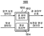
- the transparent display device 1300 includes a processor 1310, a transparent display timing controller 1321, a transparent display panel 1320, a transparent display data driver 1322, a transparent display scan driver 1323, and a light controller timing controller 1331. And an optical controller panel 1330, an optical controller data driver 1332, and an optical controller scan driver 1333.
- the timing controllers 1321 and 1331 may be configured in one integrated circuit, or may be configured by being patterned on a panel.
- the timing controllers 1321 and 1331 and the data drivers 1322 and 1332 may be a chip on glass (COG).
- COG chip on glass
- PCB Peripheral Component
- FPCB Flexible Circuit Board
- the processor 1310 provides image data to the transparent display unit timing controller 1321 and optical control data to the light control unit timing controller 1331.
- Light control data is data for selectively controlling the transmittance of incident light.
- the processor 1310 may generate a synchronization signal and provide the synchronization signal to the transparent display timing controller 1321 and the light control timing controller 1331 so that the transparent display and the light controller may be time-synchronized.
- the synchronization signal may be generated to match a panel having a slow response speed among the transparent display unit and the light control unit.
- the transparent display unit includes a transparent display unit timing controller 1321, a transparent display unit panel 1320, a transparent display unit data driver 1322, a transparent display unit scan driver 1323, and a power supply unit 1324.
- the transparent display timing controller 1321 may be referred to as a transparent display driver.
- the transparent display driver generates a scan control signal based on an image to control the transparent display scan driver 1323, and generates a data signal to generate transparent display data.
- the driver 1322 is controlled.
- the transparent display unit data driver 1322 receives a data signal from the transparent display unit timing controller 1321.
- the transparent display data driver 1322 converts the data signal through a corresponding gamma voltage and determines the amount of current flowing through the anode and the cathode of the organic light emitting diode to control the degree of emission of the corresponding pixel.
- the transparent display scan driver 1323 operates to drive a scan line so that a data signal can be input to a pixel corresponding to each scan line.
- the transparent display scan driver 1323 may provide the transparent display panel 1320 with one or a plurality of scan line signals for selecting one or a plurality of scan lines.
- the power supply 1324 supplies various voltages for the anode and the cathode of the transparent display data driver 1322, the transparent display scan driver 1323, and the transparent display panel 1320.
- the power supply unit 1324 supplies ELVDD, ELVSS, VDD, VSS, and the like.
- the transparent display panel 1320 includes a plurality of scan lines, a plurality of data lines, and a plurality of transparent display pixels.
- the switching thin film transistor T1 and the driving thin film transistor T2 are used.
- the light control unit may be configured and driven in a passive matrix.
- the light controller may be driven by an active matrix.
- the light controller timing controller 1331 receives the light control data from the processor 1310 as described above.
- the light control data is data for controlling the transmittance of the transparent display device 1300.
- the light control data is determined by the processor 1310 or the light controller timing controller 1331 of the transparent display device 1300.
- the light control unit scan driver 1333 drives the scan line so that a data signal can be input to a pixel corresponding to each scan line.
- the light control unit data driver 1332 converts the data signal into a corresponding voltage, and supplies a voltage and a pulse of the light control unit to control the spreadability of the black charged particles.
- the transparent display device 1300 may adjust the transmittance of the light control unit by adjusting the voltage or pulse that is eventually applied to the light control unit through the light control data.
- the power supply unit supplies voltages necessary for the light control unit data driver 1332 and the light control unit scan driver 1333.
- the transparent display device 1400 includes a processor 1410, a controller 1415, a transparent display unit, and a light control unit, and the transparent display unit includes a transparent display unit panel 1440 and a transparent display unit panel driver 1420. Includes a light controller panel 1450 and a light controller panel driver 1430.
- the transparent display panel 1440 and the light control panel 1450 include a plurality of pixels.
- the controller 1415 controls the operation of the transparent display device 1400 system.
- the controller 1415 may operate the system according to a user's command, and operate the system according to a preset operation.
- the controller 1415 controls the processor 1410 to lower the transmittance based on the optical characteristics from the optical sensor so as to improve the visibility of the image displayed on the transparent display device 1400. Controls the mode of the transparent display device 1400 to be operated.
- the controller 1415 may include or be integrated with the processor 1410.
- the controller 1415 of the transparent display device 1400 includes a system.
- the system includes an operating system (OS).
- the OS stage further includes a plurality of modes for providing the effect of the present invention to the user. Each mode is selected as required by the user, and in particular, the third mode is actively selected to be optimal by adapting to the surrounding environment.
- the second mode sets the light control unit to the shielded state.
- the second mode maximizes the effectiveness of the shielding. Although the visibility is improved to the maximum, there is a problem that the transparent area of all screens is shielded so that the effect of the transparent display cannot be enjoyed.
- the third mode is a mode in which the object of the input image is extracted and the transmittance of the light control unit region corresponding to the object displayed on the transparent display unit is adjusted.
- the transparent display device 1400 of the third mode minimizes the visibility deterioration due to the change in the external illuminance environment and the external environment. In this mode, the visibility of the input image is maintained while maintaining the transparent effect.
- the fourth mode is a light control mode, and the mode is configured to display an image corresponding to the resolution of the light control unit. It drives at low power by cutting off the power supply of the organic light emitting device.
- This mode is a specialized function in the outdoor environment, which is effective when the external light is quite bright, and is configured to implement an image by shading.
- the fourth mode may be selected by the user when the environment is quite bright, or operate by setting the fourth mode entrance reference illumination.
- the transparent display device 1400 may include an input unit, and the plurality of modes may be sequentially changed whenever there is an input signal through the input unit.
- a physical input unit may be useful when the visibility of the transparent display device 1400 is sharply degraded. When visibility is sharply lowered, it may be difficult for the user to select a required mode because it is difficult for the user to visualize the menu displayed on the transparent display unit.
- 15 is a conceptual diagram of a gamma curve in a transparent display device according to an embodiment of the present invention.
- the x-axis is represented by an input value of 0 to 255, and is an axis from the darkest value to the brightest value of the image.
- the y axis is normalized to the axis representing the luminance and is represented by a value of 0 to 1.0.
- the gamma curve is assumed to be a gray gamma curve.
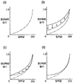
- FIG. 15A illustrates a graph of a gamma curve when the light control unit of the transparent display device adjusts light transmittance to 0% and 200 lux of external light is incident on the rear surface of the transparent display device according to an embodiment of the present invention. It is.
- the gamma value of the gamma curve illustrated in FIG. 15A may be 2.2.
- the dashed-dotted gamma curve of FIG. 15A is referred to as a target gamma curve.
- a gamma curve having a 2.2 gamma value of an image may be measured without distortion.
- light incident to the rear surface may be transmitted through the transparent display device so that an object on the rear surface of the transparent display device may be visually recognized.
- a solid line shows a graph of a gamma curve predicted under an external light incident condition of 100% light transmittance and 200 lux as a solid line.
- the dashed-dotted line is the target gamma curve of Fig. 15A.
- the dotted line is the same gamma curve as the solid line except the 40% light transmittance.
- the light control unit when the light control unit controls the light transmittance of the transparent display device to be 0% and lowers the noise, the light control unit may match the gamma curve of (a) again. As described above, the object behind the transparent display device may not be visually recognized as described above.
- the light control unit adjusts the light transmittance and changes the gamma curve through image processing on the displayed image, thereby preventing black visibility and objects on the back of the transparent display device. At the same time additional visual information can be maintained.
- a gamma curve of a dotted line may be generated.
- the dotted gamma curve is closer to the target gamma curve of the dashed line than the solid gamma curve.
- the dotted gamma curve has a higher luminance than the target gamma curve of the dashed line over the entire x-axis input value.
- the display image may be processed to increase the luminance value of the image.
- the luminance value of the image is increased, the luminance of the image is increased relative to the incident noise so that the image can be recognized more clearly, and the contrast ratio and visibility can be improved.
- the gamma curve of the dotted line in FIG. 15 (b) may be implemented by reducing the noise and increasing the brightness of the image by the light control unit.
- the gamma curve can be horizontally shifted to adjust the gamma curve to approximate the target gamma curve without further lowering the light transmittance.
- the solid line represents a gamma curve predicted under an external light incident condition of 40% light transmittance and 200 lux.
- the dashed-dotted line represents the target gamma curve of FIG. 15A.
- the dotted gamma curve represents a gamma curve predicted when the image is corrected under the conditions of the solid line.
- the correction of the image may be the correction of the gamma value.
- the correction of the gamma value may be to change the gamma value from 2.2 to 2.8 in the gamma curve function of the solid line of FIG. 15C.
- a gamma curve of a dotted line may be generated.
- the gamma curve of the dotted line may be closer to the target gamma curve of the dashed line than the gamma curve of the solid line.
- a solid line shows a gamma curve predicted under 40% light transmittance, image correction, and an external light incident condition of 200 lux.
- the dashed-dotted line represents the target gamma curve of FIG. 15A.
- the gamma curve of the solid line whose light transmittance is controlled and the image is corrected has a higher luminance than the target gamma curve at some input values, i.e., a low input value, but has substantially the same luminance as the target gamma for a predetermined value or more. .
- the transparent display device can adjust the light transmittance and correct the image, thereby making it possible to see objects on the back side and also improve the black visibility of the image.
- 16A, 16B, and 16C are conceptual views of a display image in a transparent display device according to an embodiment of the present invention.
- the display image 1610 on the left displays one object 1615.
- the display image 1610 has a characteristic of a solid line gamma curve on the right side.
- the solid line gamma curve on the right side may be a gamma curve substantially the same as the solid line gamma curve of FIG. 15B.
- the left display image 1610 and the solid gamma curve are the image and the gamma curve to which the noise incident on the rear surface of the transparent display device is applied. Due to noise incident on the rear surface of the transparent display device, the display image 1610 has a low contrast ratio and low black visibility.
- the display image 1620 on the left side displays one object 1625.
- the display image 1620 has a characteristic of a solid line gamma curve on the right side.
- the solid line gamma curve on the right may be a gamma curve substantially the same as the solid line gamma curve of FIG. 15C.
- the display image 1620 and the solid line gamma curve on the left are the image 1620 and the gamma curve in which only 40% of the noise incident on the rear surface of the transparent display device is incident by the light controller. Due to the decrease in the light transmittance, the overall gamma curve of the display image 1620 is lowered, and the contrast ratio and the visibility of black are improved.
- the display image may be processed to increase the luminance value of the image, thereby lowering the gamma curve.
- the display image 1630 on the left side displays one object 1635.
- the display image 1630 has a characteristic of a solid line gamma curve on the right side.
- the solid line gamma curve on the right side may be a gamma curve substantially the same as the solid line gamma curve of FIG. 15D.
- the display image 1630 is an image and a gamma curve whose gamma values are corrected.
- the black of the object 1635 or the darker left region of the image is more clearly expressed in the display image 1630 of FIG. 16C, but the bright portions at the right and the bottom of the image are maintained.
- the brightness contrast and black visibility are relatively improved.
- the adjustment of the light transmittance and the correction of the image are complementary to each other, and by performing both processes, both the information and the visibility of the black display that can visualize the object on the back side are performed.
- Excellent transparent display device can be implemented.
- the images 1710 and 1720 of (a) and (b) are images input from a RAM memory or the like. That is, the images 1710 and 1720 of FIGS. 17A and 17B are original image data rather than the image displayed on the transparent display device, and the histograms of FIGS. 17A and 17B are input image data. Histogram for.
- the x-axis of the histogram is represented by an input value of 0 to 255, and is an axis for the values of the darkest input value to the brightest input value of the image.
- the y-axis is the frequency of the pixel for each input value.
- the pixel frequency is low at a low input value of the image 1710. Accordingly, the image 1710 of FIG. 17A may be an image having a low contrast ratio and a low display frequency of black.
- the transparent display device may analyze the histogram 1715 of (a), detect a low frequency at a low input value, and shift or stretch the histogram 1715.
- the image (b) is an image 1720 in which the histogram 1725 is stretched to increase the pixel frequency at a low input value. Referring to the histogram 1725 of (b) of FIG. 17, the pixel frequency at a low input value is increased, and referring to the image 1720 of (b), the black display is more pronounced.
- the processing unit of the transparent display control device may process the image to improve the display of the black in the transparent display device.
- the transparent display device since the brightness displayed in the entire image is increased, when the image is displayed darker than the display in the opaque display device, visibility may be improved.
- the transparent display control device may process the image to be more suitable for the transparent display device.
- 17 illustrates a process in which the histogram 1725 is stretched, various digital signal processing methods such as histogram shifting and enhanced level adjustment may be applied.
- a transparent display device includes at least one optical sensor configured to measure color information of external light incident on a rear surface of a transparent display unit and a transparent display unit, and is incident on a rear surface of the transparent display unit to transmit the plurality of transmission units.
- the light controller may be configured to control the amount of light, and the controller may be configured to correct the light transmittance of the light controller and an image of the transparent display based on light characteristics.
- the image quality optimization and visibility improvement according to the external environment provided by the correction of the image of the transparent display unit based on the color information of the external light may be further enhanced by adjusting the amount of external light incident on the rear surface of the transparent display device through the light control unit.
- FIG. 18 is a block diagram of a transparent display control device according to an embodiment of the present invention.
- the transparent display control device 1800 includes a processing unit 1810 including a light control processing unit 1812 and an image processing unit 1814.
- the transparent display control apparatus 1800 receives pre-stored spot correction data and image data from a memory, corrects spots of the light control unit, corrects the received image, and generates a light control unit signal and a corrected image signal.
- the processor 1810 receives image data, spot correction data, and the like, and performs various signal processing on the input image and light controller signals to control the transparent display unit and the light controller.
- the image processor 1814 of the processor 1810 may correct the image signal and transmit the corrected image signal to the transparent display unit.
- the light control processor 1812 of the processor 1810 may generate a signal of the light controller and transmit the signal to the light controller.
- the image processing performed by the processor 1810 may include, for example, adjusting a gain used to adjust luminance of an image displayed on the transparent display unit, adjusting an image based on the histogram of the image, and changing a gamma curve through changing image data. And a stain correction of the light control unit.
- the light control processing unit 1812 may adjust the light control unit signal to correct the unevenness of the light control unit.
- the light control processing unit 1812 can suppress unevenness inherent in the light control panel by adjusting the signal level of the light control unit signal based on the unevenness correction data.
- the light control processor 1812 may adjust the light controller signal based on the spot correction data in data units input every clock.
- the histogram refers to data created by detecting the number of appearances of data falling into each section by, for example, 256 luminance sections.
- the image processor 1814 may process various images based on the histogram data.
- the image processor 1814 may adjust the image level in the histogram data in order to minimize burn-in of the image in the transparent display unit or to reduce power consumption.
- the image processor 1814 analyzes the histogram to detect a minimum image level, a maximum image level, or an average image level (APL), and correct the image level based on the detected image level to display the transparent display unit. The luminance of the image displayed on the screen can be corrected.
- APL average image level
- the black display since light is incident on the rear surface of the transparent display device, the black display may be substantially brighter than the black display. In addition, since the brightness displayed not only on the black display but also on the entire image is increased, in the transparent display device, the image ratio may be lower than that in the opaque display device.
- the input image may be produced or distributed without considering the transparent display device, and it may be important that the image displayed on the transparent display device is processed to have a higher contrast ratio than the image displayed on the non-transparent display device. . Therefore, the transparent display control apparatus 1800 according to an exemplary embodiment may process an image to be more suitable for the transparent display device.
- Processing the image so that the image is suitable for the transparent display device may include processing the image such that the display of a lower image level, that is, a dark area, is increased. Since the image has a different distribution of dark areas for each frame, the image may be processed for each frame, and a predetermined image processing is performed for every frame, so that the distribution of the dark areas may increase on average.
- the image processing unit 1814 measures the frequency of the image level of a certain section in the histogram of the image, and if the frequency is low in a certain section of the low image level, for example, the histogram is shifted. Can be processed in order to That is, the image processor 1814 may stretch the pixels of the image having a high image level to include a predetermined section of the low image level to process the image. When displaying an image processed by the transparent display device, an image with a clearer black display may be recognized.
- the transparent display control apparatus 1800 may adjust the gamma curve of the image to improve the display of black.
- a method of improving the display of black may vary.
- the gamma curve function is the gamma curve function.
- L (V) is an output luminance
- V is an input signal
- ⁇ is a gain
- ⁇ is an offset
- ⁇ is a gamma value.
- the transparent display control device 1800 may improve display of black on the transparent display device by changing at least one of ⁇ , ⁇ , and ⁇ .
- the contrast ratio can be adjusted, the brightness can be adjusted by adjusting the offset of ⁇ , and the data correction of the input image by adjusting ⁇ , Gamma can be adjusted.
- the image processing to make the image more suitable for the transparent display device is based on the light transmittance control by the light control unit.
- the light control unit of the transparent display device may shield at least a part of the light incident on the rear surface of the transparent display device. When part of the incident light is shielded, the display and contrast ratio of the black of the image displayed on the transparent display device may be improved.
- image processing of the input image by the image processor 1814 of the transparent display control apparatus 1800 may be based on the light transmittance of the light controller. For example, when the light transmittance of the light control unit is set to 40%, since more light is shielded than when the light transmittance is 100%, the image may be minimized to minimize distortion of the image than when the light transmittance is 100%.
- the image processing intensity for may be lower. That is, when the light transmittance of the light control unit is low, the correction of the image may be limited to minimize the distortion of the image.
- the light control processor 1812 of the transparent display control device 1800 may determine the transmittance of the light control unit based on the processed image. For example, the light control processing unit 1812 of the transparent display control device 1800 processes an image so as to be suitable for the transparent display device, but determines that a sufficient sharpness cannot be obtained. Can be controlled. Alternatively, the light control processing unit 1812 may adjust the transmittance of the light shield to be less than or equal to a predetermined transmittance.
- the preset transmittance means a target transmittance.
- the transmittance of the light shield may be determined, and an image may be image processed based on the determined transmittance, or the image may be image processed, and the transmittance of the light shield may be determined based on the image processed image.
- the transparent display control apparatus 1800 generates light control data based on the image data processed by the image processing method and the transmittance of the light control unit according to the image processing method described above.
- the generated image processed image data may be transmitted to the transparent display unit, and the generated light control signal may be transmitted to the light control unit.
- 19A and 19B are conceptual views illustrating spot correction in the light control unit of the transparent display device according to the exemplary embodiment.
- the transparent display device 1900 includes a light controller 1910, and a stain 1920 is illustrated on one surface of the light controller 1910.
- the spots 1920 may be reduced by improving the manufacturing process of the light control unit 1910, but a method of compensating the spots 1920 by correcting data driving the light control unit 1910 is also used.
- the stain 1920 may be due to the threshold voltage deviation of the driving thin film transistor of the light control unit 1910.
- the unevenness 1920 may be due to the variation in the exposure amount due to the overlapping exposure and the aberration of the multi-lenses during exposure of the exposure equipment used in the thin film pattern forming process of the light control unit 1910 manufacturing process.
- the width of the thin film pattern is changed by the variation in the exposure amount, so that the parasitic capacitance variation of the thin film transistor, the height variation of the column spacer maintaining the cell gap, and the parasitic capacitance variation between the data lines are generated.
- the stain 1920 may be displayed in an irregular irregular shape for reasons of process defects such as inflow of foreign substances as well as standard stains.
- the spots 1920 of the light controller 1910 may be corrected for uniform light transmittance control. Although correction of light emission unevenness is performed in the general display device, unevenness correction of the light controller 1910 may be more important in the transparent display device 1900.
- the transparent display device 1900 according to the exemplary embodiment of the present invention is formed such that the transparent display unit and the light control unit 1910 face each other. That is, two display units are formed in the transparent display device 1900 according to an exemplary embodiment of the present invention, and the viewer visually recognizes the light emitted or controlled by the two display units. ) May be recognized as a blot 1920 of the image displayed by the transparent display unit. Therefore, in the display device including a plurality of panels, such as the transparent display device 1900 according to an embodiment of the present invention, the uniformity of the panels becomes more important.
- the spot correction data is information for correcting the spot 1920 of the image displayed on the panel of the light controller 1910 which may appear in the process of the light controller 1910.
- a process of extracting spot correction data for all regions of the light controller 1910 may be required.
- the spot data can be extracted by directly specifying the size and level of the spot area, by using an image camera, or by measuring the threshold voltage of the driving thin film transistor.
- a light source having a constant luminance is disposed on one side of the transparent display device 1900, and an imaging unit is disposed on the opposite side of the transparent display device 1900. Since the voltage applied to each pixel of the light control unit 1910 and the light transmittance of each pixel of the light control unit 1910 have a linear relationship, the luminance incident on the imaging unit changes in proportion to the applied voltage.
- the spot correction data means that the spot 1920 is removed from the panel of the light controller 1910 when the spot 1920 is present in the image where the light controller 1910 controls the light transmittance. Correction data for correcting the input voltage with respect to the generated pixel.
- the spot correction data may be spot correction data for correcting light emission spots generated in a horizontal direction or a vertical direction, or may be spot correction data for correcting locally generated spots.
- the spot correction data is stored in a memory of the transparent display device 1900.
- the memory in which the spot correction data is stored may be a memory that can be stored without losing information even when the transparent display device 1900 is turned off.
- the memory may be, for example, an EEPROM memory, flash memory, or the like, which can electrically rewrite its contents.
- the transparent display device 1900 includes a light controller 1910, and a stain 1920 is illustrated on one surface of the light controller 1910.
- the transparent display control device is controlled to eliminate the spots 1920 by correcting the light control data input to the light control unit 1910 using the above spots correction data.
- FIG. 19B illustrates the light control unit 1930 of the transparent display device 1900 controlled by light control data with corrected spots. As the light control unit 1930 of the transparent display device 1900 according to the exemplary embodiment of the present invention is corrected for unevenness, light transmittance control of the transparent display device 1900 may be more uniformly performed.
- FIG. 20 is a schematic diagram of devices to which a transparent display device according to an embodiment of the present invention can be applied.
- the transparent device 3100 may include a transparent display device 3110, a control device 3120, and an input unit 3130.
- the transparent display device 3110 may be configured such that at least one surface of the transparent display device 3110 has only a bezel-free or minimal bezel.
- the transparent device 3100 may be implemented by the control device 3120 to utilize an augmented reality through the transparent display device 3110 or other functions of the transparent display device 3110.
- the transparent device 3100 may select various modes for controlling the transparent display device 3110 by using a separate input unit 3130 such as a button.
- Modes for controlling the transparent display device 3110 may include a power saving mode, a cinema mode, a brightness enhancement mode, and the like.
- the separate input unit 3130 may be used when it is difficult to select a control window displayed on the transparent display device 3110 because the visibility of the transparent display device 3110 is sharply degraded due to the surrounding illumination environment.
- the transparent display device 3200 may be configured to recognize an image and an object behind the transparent display device 3210 through the transparent display device 3210.
- the transparent display device 3310 is used as a display device of the transparent mobile device 3300.
- the transparent display device 3310 is illustrated to be included in the transparent mobile device 3300 in (c)
- the transparent display device 3310 is installed in a miniaturization device or a mobile device such as a smart phone, a mobile phone, a tablet PC, a PDA, and the like. Can be.
- a miniaturization device or a mobile device such as a smart phone, a mobile phone, a tablet PC, a PDA, and the like.
- elements of the transparent display device 3310 may be designed to suit a limited battery capacity.
- a touch screen for user input of the transparent mobile device 3300 may be included.
- the touch screen may be formed on the transparent display device 3310, or may be formed in an in-cell type. Also, in view of the fact that the rear surface of the transparent display device 3310 is recognizable, the touch screen may be configured to sense touches on both sides of the transparent display device 3310.
- the transparent display device 3510 may be used as part of the door 3520 of the refrigerator.
- the transparent display device 3510 may include an element that reflects energy.
- the transparent display device 3500 may be a moisture reducing coating so that objects in the refrigerator 3500 at the rear of the transparent display device 3510 are easily seen.
- FIG. 20 (f) illustrates a case where the transparent display device according to various embodiments of the present disclosure is used as an advertisement exposure apparatus 3600 of a bus stop.
- the transparent display device 3610 according to various embodiments of the present disclosure is illustrated to be included in the advertisement exposure device 3600 of the bus stop in (c)
- the transparent display device 3610 may be attached to an enlargement device or a fixing device such as a television or an electronic display board. Can be. Since external power is supplied, elements of the transparent display device 3610 may be designed so that the display device may realize higher quality under a stable supply power.
- the advertisement display apparatus of the bus stop may include a motion sensor to interact with a passing pedestrian.
- the motion sensor may include a time of flight (TOF) infrared sensor.
- TOF time of flight
- the transparent display device When used as a smart window, it may include at least a support for being used as a smart window, and the support may be used for use as a smart window such as a film, a protective film, or a protective film. It includes all kinds of film or film that can be.
- the design of the transparent display device may be partially modified by the installation place of the smart window. For example, when the transparent display device is installed in a high humidity place such as a toilet, a sink, a shower room, or a kitchen, the light control device may be designed with elements resistant to moisture.
- the transparent display device when the smart window is installed in a place where it is easily exposed to an impact from the outside such as a building exterior wall, a building glass, a vehicle glass, the transparent display device may be designed with elements that easily absorb the impact or are resistant to the impact. have.
- the smart window when used as a smart window, it can be used to attach a variety of optical films to enhance the light and / or physical properties.
- a reflective film, a diffuser film, a prism film, a lens pattern composite film, a double brightness enhancement film, an antireflective coating film, an ultraviolet blocking film, an infrared blocking film, and the like may be attached to reinforce light and / or physical properties.
- the smart window to which the transparent display device is attached may be used as a window, a smart door, a projection wall, and a smart mirror of a car.
- the steps of a method or algorithm described in connection with the embodiments disclosed herein may be embodied directly in hardware, software module, or a combination of the two executed by a processor.
- the software module may reside in RAM memory, flash memory, ROM memory, EPROM memory, EEPROM memory, registers, hard disk, removable disk, CD-ROM, or any other form of storage medium known in the art.
- An exemplary storage medium is coupled to the processor, which can read information from and write information to the storage medium.
- the storage medium may be integral to the processor.
- the processor and the storage medium may reside in an application specific integrated circuit (ASIC).
- the ASIC may reside in a user terminal.
- the processor and the storage medium may reside as discrete components in a user terminal.
- control unit is configured to vary the image displayed by the plurality of pixels by varying the gamma curve of each of the red, green and blue based on the optical characteristics.
- the controller is configured to increase the maximum brightness of the image displayed by the plurality of pixels by varying each gamma curve.
- control unit is configured to control the light control unit to maintain the transmittance of the light control unit below the predetermined transmittance based on the optical characteristics.
- control unit is configured to adjust the gamma curve of each of the red, green and blue to approximate the target gamma curve.
- control unit is configured to image the image
- transmittance of the light control unit is configured based on the image processed image
- control unit is configured to determine the transmittance of the light control unit, and to image the image based on the determined transmittance.
- the controller is configured to correct the image by analyzing the histogram of the image.
- the at least one optical sensor is configured to measure the illuminance of light incident on the back side of the transparent display.
- control unit is configured to control the light control unit to selectively shield the light incident to the transparent display unit.
- control unit is configured to image the image to be displayed on the plurality of pixels by comparing the color information of the external light with a predetermined threshold value.
- control unit is configured to subtract the brightness values of the plurality of pixels by weighting each of the color information of the external light.
- control unit is configured to completely limit the light emission of the pixel of the color corresponding to the color information of the external light, when the color information of the external light is higher than the color information of the image displayed by the plurality of pixels.
- the light control unit further comprises a light control unit configured to control the amount of light incident on the back of the transparent display portion and transmitted through the plurality of transmission units, wherein the control unit is configured to adjust the transmittance of the light control unit based on the color information It features.
Landscapes
- Engineering & Computer Science (AREA)
- Physics & Mathematics (AREA)
- Computer Hardware Design (AREA)
- General Physics & Mathematics (AREA)
- Theoretical Computer Science (AREA)
- Control Of Indicators Other Than Cathode Ray Tubes (AREA)
- Control Of El Displays (AREA)
- Electroluminescent Light Sources (AREA)
Abstract
Description
| 조도환경 | 200 lux | 2000 lux | ||||
| 화이트(nit) | 블랙(nit) | 명암비 | 화이트(nit) | 블랙(nit) | 명암비 | |
| 전면 입사 | 200 | 3 | 66.66 | 400 | 203 | 1.97 |
| 후면 입사 | 240 | 40 | 6 | 600 | 400 | 1.5 |
Claims (20)
- 영상을 표시하도록 구성된 복수의 화소와 상기 복수의 화소에 인접하여 배치된 복수의 투과부를 포함하는 투명표시부;상기 투명표시부의 배면에 입사되는 광특성을 측정하도록 구성된 적어도 하나의 광센서;상기 투명표시부의 배면에 입사되어 상기 복수의 투과부를 투과하는 광량을 제어하도록 구성된 광제어부; 및상기 광특성을 기초로 상기 광제어부 투과율 및 상기 투명표시부의 영상을 보정하도록 구성된 제어부를 포함하는, 투명표시장치.
- 제1항에 있어서,상기 제어부는 상기 광특성에 기초하여 적색, 녹색 및 청색 각각의 감마커브를 각각 가변하여 상기 복수의 화소가 표시하는 영상이 가변되도록 구성된, 투명표시장치.
- 제2항에 있어서,상기 제어부는 상기 각각의 감마커브를 각각 가변하여 상기 복수의 화소가 표시하는 상기 영상의 최대 휘도를 높이도록 구성된, 투명표시장치.
- 제2항에 있어서,상기 제어부는 상기 광특성에 기초하여 상기 광제어부의 투과율을 기 설정된 투과율 이하로 유지하도록 상기 광제어부를 제어하도록 구성된, 투명표시장치.
- 제2항에 있어서,상기 제어부는 적색, 녹색 및 청색 각각의 감마커브를 목표감마커브에 근사하게 조정되도록 구성된, 투명표시장치.
- 제1항에 있어서,상기 제어부는 상기 영상을 영상 처리하고, 영상 처리된 상기 영상에 기초하여 상기 광제어부의 투과율이 결정되도록 구성된, 투명표시장치.
- 제1항에 있어서,상기 제어부는 상기 광제어부의 투과율을 결정하고, 결정된 상기 투과율에 기초하여 상기 영상이 영상처리되도록 구성된, 투명표시장치.
- 제1항에 있어서,상기 제어부는 상기 영상의 히스토그램을 분석하여 상기 영상을 보정하도록 구성된, 투명표시장치.
- 제1항에 있어서,상기 적어도 하나의 광센서는 투명 표시부의 배면에 입사되는 광의 조도를 측정하도록 구성된, 투명표시장치.
- 제1항에 있어서,상기 제어부는 상기 투명표시부로 입사되는 광을 선택적으로 차폐하도록 상기 광제어부를 제어하도록 구성된, 투명표시장치.
- 제9항에 있어서,상기 제어부는 얼룩 보정 정보에 기초하여 상기 광제어부의 투과율을 보정하도록 구성된, 투명표시장치.
- 영상을 표시하도록 구성된 복수의 화소와 상기 복수의 화소에 인접하여 배치된 복수의 투과부를 포함하는 투명표시부;상기 투명표시부의 배면에 입사되는 외광의 컬러정보를 측정하도록 구성된 적어도 하나의 광센서; 및상기 외광의 컬러정보를 기초로 상기 투명표시부의 영상을 보정하도록 구성된 제어부를 포함하는, 투명표시장치.
- 제12항에 있어서,상기 제어부는 상기 외광의 컬러정보를 기 설정된 임계값과 비교하여 상기 복수의 화소에 표시할 상기 영상을 영상처리하도록 구성된, 투명표시장치.
- 제13항에 있어서,상기 제어부는 적어도 하나의 상기 외광의 컬러정보가 상기 기 설정된 임계값 이상인 경우, 상기 외광의 컬러정보에 대응하는 컬러의 화소의 밝기를 낮추도록 구성된, 투명표시장치.
- 제14항에 있어서,상기 제어부는 밝기가 낮아진 상기 화소를 제외한 적어도 하나의 다른 컬러의 화소의 밝기를 높이도록 구성된, 투명표시장치.
- 제12항에 있어서,상기 제어부는 상기 외광의 컬러정보에 따라 인접한 각각의 상기 복수의 화소의 밝기 값의 차감 정도가 각각 대응되어 조정하도록 구성된, 투명표시장치
- 제16항에 있어서,상기 제어부는 상기 외광의 컬러정보 각각에 가중치를 주어 상기 복수의 화소의 밝기 값을 차감하도록 구성된, 투명표시장치.
- 제12항에 있어서,상기 제어부는 상기 외광의 컬러정보에 기초하여 상기 영상의 밝기를 제한함으로써 상기 영상의 컬러 왜곡을 보정하도록 구성된, 투명표시장치.
- 제18항에 있어서,상기 제어부는 상기 외광의 컬러정보가 상기 복수의 화소가 표시하는 상기 영상의 컬러정보 보다 높은 경우, 상기 외광의 컬러정보에 대응되는 컬러의 화소의 발광을 완전히 제한하도록 구성된, 투명표시장치
- 제12항에 있어서,상기 투명표시부의 배면에 입사되어 상기 복수의 투과부를 투과하는 광량을 제어하도록 구성된 광제어부를 더 포함하고,상기 제어부는 상기 컬러정보를 기초로 상기 광제어부의 투과율을 조정하도록 구성된 것을 특징으로 하는, 투명표시장치.
Priority Applications (3)
| Application Number | Priority Date | Filing Date | Title |
|---|---|---|---|
| US14/758,751 US10217392B2 (en) | 2012-12-31 | 2013-12-30 | Transparent display device and method for controlling same |
| KR1020157021927A KR101787856B1 (ko) | 2012-12-31 | 2013-12-30 | 투명표시장치 및 그 제어 방법 |
| EP13869681.0A EP2940680B1 (en) | 2012-12-31 | 2013-12-30 | Transparent display device and method for controlling same |
Applications Claiming Priority (4)
| Application Number | Priority Date | Filing Date | Title |
|---|---|---|---|
| KR10-2012-0157803 | 2012-12-31 | ||
| KR10-2012-0157790 | 2012-12-31 | ||
| KR20120157803 | 2012-12-31 | ||
| KR20120157790 | 2012-12-31 |
Publications (1)
| Publication Number | Publication Date |
|---|---|
| WO2014104858A1 true WO2014104858A1 (ko) | 2014-07-03 |
Family
ID=51021787
Family Applications (1)
| Application Number | Title | Priority Date | Filing Date |
|---|---|---|---|
| PCT/KR2013/012398 WO2014104858A1 (ko) | 2012-12-31 | 2013-12-30 | 투명표시장치 및 그 제어 방법 |
Country Status (4)
| Country | Link |
|---|---|
| US (1) | US10217392B2 (ko) |
| EP (1) | EP2940680B1 (ko) |
| KR (1) | KR101787856B1 (ko) |
| WO (1) | WO2014104858A1 (ko) |
Cited By (4)
| Publication number | Priority date | Publication date | Assignee | Title |
|---|---|---|---|---|
| CN105353533A (zh) * | 2014-08-20 | 2016-02-24 | 群创光电股份有限公司 | 显示面板及使用其的显示设备 |
| WO2016093633A1 (ko) * | 2014-12-12 | 2016-06-16 | 삼성전자 주식회사 | 컨텐트를 표시하는 방법 및 디바이스 |
| WO2017043823A1 (ko) * | 2015-09-07 | 2017-03-16 | 엘지이노텍 주식회사 | 감지 장치 |
| KR20170033051A (ko) * | 2015-09-16 | 2017-03-24 | 엘지이노텍 주식회사 | 감지 장치 |
Families Citing this family (47)
| Publication number | Priority date | Publication date | Assignee | Title |
|---|---|---|---|---|
| KR101954749B1 (ko) * | 2014-04-01 | 2019-03-06 | 삼성전자주식회사 | 냉장고 및 그 제어방법 |
| KR102280452B1 (ko) * | 2014-11-05 | 2021-07-23 | 삼성디스플레이 주식회사 | 표시장치 및 그의 구동방법 |
| KR102389626B1 (ko) * | 2014-12-11 | 2022-04-25 | 삼성디스플레이 주식회사 | 표시 패널 및 표시 패널을 포함하는 유기 발광 표시 장치 |
| KR20160096487A (ko) * | 2015-02-05 | 2016-08-16 | 삼성전자주식회사 | 식품 보관용 저장 용기, 그 저장 용기의 관리 방법 및 냉장고 |
| US10553142B2 (en) * | 2015-08-19 | 2020-02-04 | Valve Corporation | Systems and methods for detection and/or correction of pixel luminosity and/or chrominance response variation in displays |
| KR102395794B1 (ko) * | 2015-10-13 | 2022-05-10 | 삼성전자주식회사 | 화면 출력 제어 방법 및 이를 지원하는 전자 장치 |
| JP6406221B2 (ja) * | 2015-11-17 | 2018-10-17 | 三菱電機株式会社 | 半導体装置の評価装置及び評価方法 |
| KR101954874B1 (ko) * | 2016-01-05 | 2019-05-30 | 엘지전자 주식회사 | 냉장고 |
| KR102499305B1 (ko) * | 2016-01-21 | 2023-02-14 | 삼성디스플레이 주식회사 | 표시 장치, 표시 장치의 구동 방법, 및 표시 장치를 포함하는 전자 장치 |
| KR102529665B1 (ko) | 2016-07-07 | 2023-05-10 | 삼성디스플레이 주식회사 | 투명 표시 장치 |
| CN106101594B (zh) * | 2016-08-04 | 2019-03-12 | 深圳创维-Rgb电子有限公司 | Hdr电视机及区域调光方法 |
| CN106205555A (zh) * | 2016-08-30 | 2016-12-07 | 武汉华星光电技术有限公司 | 显示装置及其亮度调整方法 |
| KR102497663B1 (ko) * | 2016-09-30 | 2023-02-07 | 엘지디스플레이 주식회사 | 투명표시장치 및 그의 구동방법 |
| KR102599536B1 (ko) * | 2017-01-26 | 2023-11-08 | 삼성전자 주식회사 | 생체 센서를 갖는 전자 장치 |
| KR102259693B1 (ko) * | 2017-03-15 | 2021-06-02 | 삼성전자주식회사 | 투명 디스플레이 장치 및 그의 디스플레이 방법 |
| KR102349384B1 (ko) | 2017-03-15 | 2022-01-11 | 삼성전자주식회사 | 투명 디스플레이 장치, 그 제어 방법 및 컴퓨터 판독가능 기록 매체 |
| CN107039018B (zh) * | 2017-05-27 | 2019-04-30 | 深圳市华星光电半导体显示技术有限公司 | 透明显示器色温调整系统及透明显示器色温调整方法 |
| CN109102758B (zh) * | 2017-06-20 | 2021-08-17 | 天马微电子股份有限公司 | 显示装置 |
| NL2019451B1 (en) * | 2017-08-25 | 2019-03-07 | Videowindow B V | Dynamic shading system |
| US10446117B2 (en) | 2017-10-02 | 2019-10-15 | Microsoft Technology Licensing, Llc | Manufacture and optical calibration methods for displays |
| TWI660634B (zh) * | 2017-12-26 | 2019-05-21 | Industrial Technology Research Institute | 雙介質顯示面板之驅動方法及應用其之電子裝置及顯示系統 |
| CN108172197A (zh) * | 2017-12-29 | 2018-06-15 | 深圳市华星光电半导体显示技术有限公司 | 显示器色温调整方法、电子设备及计算机可读存储介质 |
| US10761636B2 (en) * | 2018-03-08 | 2020-09-01 | Capital One Services, Llc | Systems and methods for providing an interactive user interface using a film and projector |
| US20190313086A1 (en) * | 2018-04-09 | 2019-10-10 | Kristina Contreras | System and method for generating virtual objects in a reflective augmented reality system |
| DE102018206656B4 (de) * | 2018-04-30 | 2024-03-21 | Audi Ag | Anzeigevorrichtung für ein Kraftfahrzeug und Kraftfahrzeug |
| KR102563638B1 (ko) * | 2018-07-27 | 2023-08-07 | 삼성전자주식회사 | 전자 장치에서 디스플레이 번인 방지 방법 및 전자 장치 |
| KR102705271B1 (ko) * | 2018-11-14 | 2024-09-11 | 삼성디스플레이 주식회사 | 표시 장치 |
| CN109272935B (zh) * | 2018-11-23 | 2021-04-02 | 上海天马有机发光显示技术有限公司 | 显示面板的驱动方法、驱动芯片及显示装置 |
| EP3659847B1 (en) * | 2018-11-30 | 2020-10-07 | Audi Ag | Display device for a motor vehicle, method for operating a display of a motor vehicle, control module, and motor vehicle |
| US11151628B2 (en) | 2019-03-01 | 2021-10-19 | Capital One Services, Llc | Proximity-based vehicle comparison |
| US11740723B2 (en) | 2019-05-02 | 2023-08-29 | Apple Inc. | Electronic devices having light sensors overlapped by displays |
| KR102716940B1 (ko) | 2019-07-04 | 2024-10-11 | 엘지디스플레이 주식회사 | 투명 디스플레이 영상 보정 장치 및 이를 이용한 투명 디스플레이 장치와 그의 구동방법 |
| TWI717824B (zh) | 2019-09-04 | 2021-02-01 | 財團法人工業技術研究院 | 資訊顯示方法以及資訊顯示系統 |
| WO2021066789A1 (en) * | 2019-09-30 | 2021-04-08 | Hewlett-Packard Development Company, L.P. | Programmable film display system |
| US20220383632A1 (en) * | 2019-11-27 | 2022-12-01 | Sony Group Corporation | Information processing apparatus, information processing method, and program |
| KR102692177B1 (ko) * | 2019-12-26 | 2024-08-06 | 주식회사 엘엑스세미콘 | 무라 보상 회로 및 그를 채용한 디스플레이를 위한 구동 장치 |
| KR102692179B1 (ko) * | 2019-12-26 | 2024-08-06 | 주식회사 엘엑스세미콘 | 무라 보상 회로 및 그를 채용한 디스플레이를 위한 구동 장치 |
| KR20210094956A (ko) * | 2020-01-22 | 2021-07-30 | 삼성전자주식회사 | 디스플레이를 포함하는 전자 장치 및 전자 장치의 동작 방법 |
| EP3943988B1 (en) * | 2020-07-20 | 2023-12-27 | Samsung Electronics Co., Ltd. | Spectral filter, and image sensor and electronic device including the spectral filter |
| CN112083339B (zh) * | 2020-09-13 | 2024-04-30 | 巨安储能武汉科技有限责任公司 | 一种电池荷电状态监测方法 |
| KR20230027392A (ko) * | 2021-08-18 | 2023-02-28 | 삼성디스플레이 주식회사 | 표시 장치 및 이의 구동 방법 |
| US11580923B1 (en) | 2021-10-13 | 2023-02-14 | Videowindow B.V. | Dynamic shading system |
| US11940613B2 (en) * | 2021-10-29 | 2024-03-26 | L3Harris Technologies, Inc. | Localized brightness control in bi-directional display with detector |
| TW202331352A (zh) * | 2021-11-17 | 2023-08-01 | 美商元平台技術有限公司 | 在用於沉浸式實境應用的智能眼鏡中基於環境光感測器和相機的顯示調整 |
| US20230152587A1 (en) * | 2021-11-17 | 2023-05-18 | Meta Platforms Technologies, Llc | Ambient light sensors and camera-based display adjustment in smart glasses for immersive reality applications |
| WO2024101491A1 (ko) * | 2022-11-11 | 2024-05-16 | 엘지전자 주식회사 | 투명 디스플레이 장치 및 그의 동작 방법 |
| CN116631313B (zh) * | 2023-07-25 | 2023-10-13 | 中电创达(深圳)实业有限公司 | 一种液晶面板的色彩校正方法及系统 |
Citations (5)
| Publication number | Priority date | Publication date | Assignee | Title |
|---|---|---|---|---|
| US20030184659A1 (en) * | 2002-04-02 | 2003-10-02 | Michael Skow | Digital color image pre-processing |
| WO2005024501A1 (en) * | 2003-09-11 | 2005-03-17 | Koninklijke Philips Electronics N.V. | Transparent display device |
| KR20060103528A (ko) * | 2003-11-19 | 2006-10-02 | 가부시키가이샤 나나오 | 액정 표시 장치의 경년 변화 보상 방법, 액정 표시 장치의 경년 변화 보상 장치, 컴퓨터 프로그램 및 액정 표시 장치 |
| KR20070072188A (ko) * | 2005-12-30 | 2007-07-04 | 엘지.필립스 엘시디 주식회사 | 엘이디 백라이트의 광센서를 이용한 액정표시장치 |
| JP2011237696A (ja) * | 2010-05-12 | 2011-11-24 | Sharp Corp | 表示装置 |
Family Cites Families (28)
| Publication number | Priority date | Publication date | Assignee | Title |
|---|---|---|---|---|
| US6362835B1 (en) * | 1993-11-23 | 2002-03-26 | Texas Instruments Incorporated | Brightness and contrast control for a digital pulse-width modulated display system |
| US5757127A (en) * | 1994-06-10 | 1998-05-26 | Nippondenso Co., Ltd. | Transparent thin-film EL display apparatus with ambient light adaptation means |
| KR100578855B1 (ko) | 2004-08-13 | 2006-05-11 | 삼성에스디아이 주식회사 | 플라즈마 표시 장치 및 그의 잔상 제거 방법 |
| US7586653B2 (en) * | 2005-04-22 | 2009-09-08 | Lexmark International, Inc. | Method and system for enhancing an image using luminance scaling |
| TWI302286B (en) * | 2005-05-19 | 2008-10-21 | Au Optronics Corp | Method of determining oled driving signal |
| KR20070020996A (ko) * | 2005-08-17 | 2007-02-22 | 삼성전자주식회사 | 칼라 에러 보정장치 및 그 방법 |
| TW200732733A (en) | 2006-02-17 | 2007-09-01 | Ind Tech Res Inst | Hybrid display |
| JP5230910B2 (ja) * | 2006-05-30 | 2013-07-10 | ペンタックスリコーイメージング株式会社 | 透過型表示装置 |
| EP2129090B1 (en) * | 2008-05-29 | 2016-06-15 | LG Electronics Inc. | Mobile terminal and display control method thereof |
| US8610654B2 (en) * | 2008-07-18 | 2013-12-17 | Sharp Laboratories Of America, Inc. | Correction of visible mura distortions in displays using filtered mura reduction and backlight control |
| KR101289653B1 (ko) * | 2008-12-26 | 2013-07-25 | 엘지디스플레이 주식회사 | 액정표시장치 |
| JP2010164782A (ja) * | 2009-01-15 | 2010-07-29 | Brother Ind Ltd | 画像表示装置 |
| US20100320919A1 (en) | 2009-06-22 | 2010-12-23 | Nokia Corporation | Method and apparatus for modifying pixels based at least in part on ambient light level |
| CN102893321A (zh) | 2010-05-12 | 2013-01-23 | 夏普株式会社 | 显示装置 |
| JP2012033213A (ja) * | 2010-07-29 | 2012-02-16 | Hitachi Media Electoronics Co Ltd | 光学的情報記録再生装置 |
| JP2012252091A (ja) * | 2011-06-01 | 2012-12-20 | Sony Corp | 表示装置 |
| KR101885698B1 (ko) * | 2011-06-27 | 2018-08-07 | 삼성디스플레이 주식회사 | 광투과율 제어가 가능한 표시장치 |
| KR101850994B1 (ko) * | 2011-11-18 | 2018-04-23 | 삼성디스플레이 주식회사 | 표시 장치의 휘도 조절 방법 및 이를 이용한 표시 장치 |
| KR20130064486A (ko) * | 2011-12-08 | 2013-06-18 | 삼성디스플레이 주식회사 | 광투과율 제어가 가능한 표시장치 |
| KR101268537B1 (ko) * | 2012-01-18 | 2013-05-28 | 한국전자통신연구원 | 디스플레이 장치 |
| KR20130094095A (ko) * | 2012-02-15 | 2013-08-23 | 삼성디스플레이 주식회사 | 투명 디스플레이 장치 및 그것의 동작 방법 |
| US9240162B2 (en) * | 2012-12-31 | 2016-01-19 | Lg Display Co., Ltd. | Transparent display apparatus and method for controlling the same |
| WO2015048911A1 (en) * | 2013-10-04 | 2015-04-09 | University Of Manitoba | Color correction method for optical see-through displays |
| KR20150140514A (ko) * | 2014-06-05 | 2015-12-16 | 삼성디스플레이 주식회사 | 투명 디스플레이 장치의 색 보상 방법 |
| KR102347780B1 (ko) * | 2015-08-25 | 2022-01-07 | 삼성디스플레이 주식회사 | 투명 표시 장치 및 이의 영상 보상 방법 |
| KR102499305B1 (ko) * | 2016-01-21 | 2023-02-14 | 삼성디스플레이 주식회사 | 표시 장치, 표시 장치의 구동 방법, 및 표시 장치를 포함하는 전자 장치 |
| KR102259693B1 (ko) * | 2017-03-15 | 2021-06-02 | 삼성전자주식회사 | 투명 디스플레이 장치 및 그의 디스플레이 방법 |
| KR102349384B1 (ko) * | 2017-03-15 | 2022-01-11 | 삼성전자주식회사 | 투명 디스플레이 장치, 그 제어 방법 및 컴퓨터 판독가능 기록 매체 |
-
2013
- 2013-12-30 US US14/758,751 patent/US10217392B2/en active Active
- 2013-12-30 WO PCT/KR2013/012398 patent/WO2014104858A1/ko active Application Filing
- 2013-12-30 EP EP13869681.0A patent/EP2940680B1/en active Active
- 2013-12-30 KR KR1020157021927A patent/KR101787856B1/ko active IP Right Grant
Patent Citations (5)
| Publication number | Priority date | Publication date | Assignee | Title |
|---|---|---|---|---|
| US20030184659A1 (en) * | 2002-04-02 | 2003-10-02 | Michael Skow | Digital color image pre-processing |
| WO2005024501A1 (en) * | 2003-09-11 | 2005-03-17 | Koninklijke Philips Electronics N.V. | Transparent display device |
| KR20060103528A (ko) * | 2003-11-19 | 2006-10-02 | 가부시키가이샤 나나오 | 액정 표시 장치의 경년 변화 보상 방법, 액정 표시 장치의 경년 변화 보상 장치, 컴퓨터 프로그램 및 액정 표시 장치 |
| KR20070072188A (ko) * | 2005-12-30 | 2007-07-04 | 엘지.필립스 엘시디 주식회사 | 엘이디 백라이트의 광센서를 이용한 액정표시장치 |
| JP2011237696A (ja) * | 2010-05-12 | 2011-11-24 | Sharp Corp | 表示装置 |
Non-Patent Citations (1)
| Title |
|---|
| See also references of EP2940680A4 * |
Cited By (7)
| Publication number | Priority date | Publication date | Assignee | Title |
|---|---|---|---|---|
| CN105353533A (zh) * | 2014-08-20 | 2016-02-24 | 群创光电股份有限公司 | 显示面板及使用其的显示设备 |
| CN105353533B (zh) * | 2014-08-20 | 2019-11-12 | 群创光电股份有限公司 | 显示面板及使用其的显示设备 |
| WO2016093633A1 (ko) * | 2014-12-12 | 2016-06-16 | 삼성전자 주식회사 | 컨텐트를 표시하는 방법 및 디바이스 |
| US10423223B2 (en) | 2014-12-12 | 2019-09-24 | Samsung Electronics Co., Ltd. | Method and device for displaying content |
| WO2017043823A1 (ko) * | 2015-09-07 | 2017-03-16 | 엘지이노텍 주식회사 | 감지 장치 |
| KR20170033051A (ko) * | 2015-09-16 | 2017-03-24 | 엘지이노텍 주식회사 | 감지 장치 |
| KR102496006B1 (ko) | 2015-09-16 | 2023-02-17 | 엘지이노텍 주식회사 | 감지 장치 |
Also Published As
| Publication number | Publication date |
|---|---|
| US20150371579A1 (en) | 2015-12-24 |
| EP2940680A1 (en) | 2015-11-04 |
| KR20150136052A (ko) | 2015-12-04 |
| EP2940680A4 (en) | 2016-08-31 |
| US10217392B2 (en) | 2019-02-26 |
| KR101787856B1 (ko) | 2017-11-15 |
| EP2940680B1 (en) | 2019-03-13 |
Similar Documents
| Publication | Publication Date | Title |
|---|---|---|
| WO2014104858A1 (ko) | 투명표시장치 및 그 제어 방법 | |
| WO2014157930A1 (en) | Image processing method and apparatus for display devices | |
| AU2017413152B2 (en) | Electronic apparatus and method for displaying a content screen on the electronic apparatus thereof | |
| WO2014104850A1 (en) | Transparent display apparatus and method for controlling the same | |
| WO2019132485A1 (en) | Image processing apparatus, image processing method and multi-screen display | |
| WO2020071594A1 (en) | Display panel and method for driving the display panel | |
| WO2020071595A1 (en) | Display panel and method for driving the display panel | |
| WO2016195301A1 (en) | Display system for enhancing visibility and methods thereof | |
| WO2014104802A1 (en) | Transparent display apparatus and method for controlling the same | |
| WO2014168454A1 (en) | Electronic device, display controlling apparatus and method thereof | |
| WO2018124784A1 (en) | Display apparatus and display method | |
| WO2020085768A1 (en) | Display apparatus and method for driving same | |
| WO2018110968A1 (en) | Display apparatus and method of controlling the same | |
| WO2020209464A1 (en) | Liquid crystal display device | |
| WO2019098513A1 (ko) | 디스플레이 장치 및 그 제어 방법 | |
| WO2022181962A1 (ko) | 디스플레이 장치 및 그 광원 장치 | |
| WO2022231088A1 (ko) | 디스플레이 장치 및 그의 동작 방법 | |
| WO2022075573A1 (ko) | 디스플레이 장치 | |
| WO2022035052A1 (ko) | 디스플레이 장치 및 이의 제어 방법 | |
| WO2023229159A1 (ko) | 디스플레이 장치 및 그 제어방법 | |
| WO2024029778A1 (ko) | 디스플레이를 포함하는 전자 장치 및 이의 동작 방법 | |
| WO2023003055A1 (ko) | 영상표시장치 | |
| WO2021060703A1 (en) | Display device and controlling method thereof | |
| WO2021060726A1 (en) | Display apparatus and control method thereof | |
| WO2022124496A1 (ko) | 평판패널 및 이를 포함하는 스캐닝 장치 |
Legal Events
| Date | Code | Title | Description |
|---|---|---|---|
| 121 | Ep: the epo has been informed by wipo that ep was designated in this application |
Ref document number: 13869681 Country of ref document: EP Kind code of ref document: A1 |
|
| NENP | Non-entry into the national phase |
Ref country code: DE |
|
| WWE | Wipo information: entry into national phase |
Ref document number: 14758751 Country of ref document: US Ref document number: 2013869681 Country of ref document: EP |
|
| ENP | Entry into the national phase |
Ref document number: 20157021927 Country of ref document: KR Kind code of ref document: A |