WO2014098060A1 - 磁気共鳴イメージング装置及び磁気共鳴イメージング方法 - Google Patents
磁気共鳴イメージング装置及び磁気共鳴イメージング方法 Download PDFInfo
- Publication number
- WO2014098060A1 WO2014098060A1 PCT/JP2013/083701 JP2013083701W WO2014098060A1 WO 2014098060 A1 WO2014098060 A1 WO 2014098060A1 JP 2013083701 W JP2013083701 W JP 2013083701W WO 2014098060 A1 WO2014098060 A1 WO 2014098060A1
- Authority
- WO
- WIPO (PCT)
- Prior art keywords
- signal
- magnetic resonance
- generated
- frequency
- clock
- Prior art date
- Legal status (The legal status is an assumption and is not a legal conclusion. Google has not performed a legal analysis and makes no representation as to the accuracy of the status listed.)
- Ceased
Links
Images


Classifications
-
- G—PHYSICS
- G01—MEASURING; TESTING
- G01R—MEASURING ELECTRIC VARIABLES; MEASURING MAGNETIC VARIABLES
- G01R33/00—Arrangements or instruments for measuring magnetic variables
- G01R33/20—Arrangements or instruments for measuring magnetic variables involving magnetic resonance
- G01R33/28—Details of apparatus provided for in groups G01R33/44 - G01R33/64
- G01R33/32—Excitation or detection systems, e.g. using radio frequency signals
- G01R33/36—Electrical details, e.g. matching or coupling of the coil to the receiver
- G01R33/3621—NMR receivers or demodulators, e.g. preamplifiers, means for frequency modulation of the MR signal using a digital down converter, means for analog to digital conversion [ADC] or for filtering or processing of the MR signal such as bandpass filtering, resampling, decimation or interpolation
-
- A—HUMAN NECESSITIES
- A61—MEDICAL OR VETERINARY SCIENCE; HYGIENE
- A61B—DIAGNOSIS; SURGERY; IDENTIFICATION
- A61B5/00—Measuring for diagnostic purposes; Identification of persons
- A61B5/05—Detecting, measuring or recording for diagnosis by means of electric currents or magnetic fields; Measuring using microwaves or radio waves
- A61B5/055—Detecting, measuring or recording for diagnosis by means of electric currents or magnetic fields; Measuring using microwaves or radio waves involving electronic [EMR] or nuclear [NMR] magnetic resonance, e.g. magnetic resonance imaging
-
- A—HUMAN NECESSITIES
- A61—MEDICAL OR VETERINARY SCIENCE; HYGIENE
- A61B—DIAGNOSIS; SURGERY; IDENTIFICATION
- A61B5/00—Measuring for diagnostic purposes; Identification of persons
- A61B5/72—Signal processing specially adapted for physiological signals or for diagnostic purposes
- A61B5/7203—Signal processing specially adapted for physiological signals or for diagnostic purposes for noise prevention, reduction or removal
-
- G—PHYSICS
- G01—MEASURING; TESTING
- G01R—MEASURING ELECTRIC VARIABLES; MEASURING MAGNETIC VARIABLES
- G01R33/00—Arrangements or instruments for measuring magnetic variables
- G01R33/20—Arrangements or instruments for measuring magnetic variables involving magnetic resonance
- G01R33/28—Details of apparatus provided for in groups G01R33/44 - G01R33/64
- G01R33/32—Excitation or detection systems, e.g. using radio frequency signals
- G01R33/36—Electrical details, e.g. matching or coupling of the coil to the receiver
- G01R33/3678—Electrical details, e.g. matching or coupling of the coil to the receiver involving quadrature drive or detection, e.g. a circularly polarized RF magnetic field
Definitions
- Embodiments described herein relate generally to a magnetic resonance imaging (MRI: Magnetic Resonance Imaging) apparatus and a magnetic resonance imaging method.
- MRI Magnetic Resonance Imaging
- the MRI system magnetically excites the nuclear spin of a subject placed in a static magnetic field with a radio frequency (RF) signal of Larmor frequency, and nuclear magnetic resonance (NMR) generated by this excitation.
- RF radio frequency
- NMR nuclear magnetic resonance
- the direct sampling method is a signal processing method in which an analog signal is detected by direct AD (analog-to-digital) conversion without performing frequency conversion.
- direct sampling of MR signals is performed, digital signal detection is performed using an MR signal detection carrier created by a direct digital synthesizer (DDS: direct digital synthesizer).
- DDS direct digital synthesizer
- the present invention provides a magnetic resonance imaging apparatus and a magnetic resonance imaging method capable of acquiring an MR signal in which noise and error are further reduced when receiving an MR signal by a direct sampling method. Objective.
- a magnetic resonance imaging apparatus includes a data acquisition unit and an image generation unit.
- the data collection unit collects magnetic resonance signals from the subject.
- the image generation unit generates magnetic resonance image data based on the magnetic resonance signal.
- the data collection unit includes a conversion unit, a separation unit, and a filter processing unit.
- the conversion unit converts the analog magnetic resonance signal received by the high frequency coil into the digital magnetic resonance signal without down-conversion.
- the separation unit separates the digital magnetic resonance signal into an in-phase signal and a quadrature signal.
- the filter processing unit performs a filter process for removing noise on the in-phase signal and the quadrature signal.
- the magnetic resonance imaging apparatus includes a data acquisition unit and an image generation unit.
- the data collection unit collects magnetic resonance signals from the subject.
- the image generation unit generates magnetic resonance image data based on the magnetic resonance signal.
- the data collection unit includes a conversion unit and a correction unit.
- the conversion unit converts the analog magnetic resonance signal received by the high frequency coil into the digital magnetic resonance signal without down-conversion.
- the correction unit is a detection carrier for a magnetic resonance signal corresponding to a high-frequency transmission signal in which a clock of a transmission carrier is generated by a method other than a generation method by a direct digital synthesizer among the digital magnetic resonance signals, The phase error of the clock of the detection carrier for which the clock is generated by the generation method by the digital synthesizer is corrected based on the clock generated by a method other than the generation method by the direct digital synthesizer.
- the magnetic resonance imaging method includes a step of collecting a magnetic resonance signal from a subject, and a step of generating magnetic resonance image data based on the magnetic resonance signal.
- the generation of the magnetic resonance image data includes the step of converting the analog magnetic resonance signal received by the high frequency coil into the digital magnetic resonance signal without down-conversion, and the digital magnetic resonance signal. Separating the phase signal into a quadrature phase signal and performing a noise removal filter process on the in-phase signal and the quadrature signal.
- the magnetic resonance imaging method includes a step of collecting a magnetic resonance signal from a subject, and a step of generating magnetic resonance image data based on the magnetic resonance signal.
- the magnetic resonance image data is generated by converting the analog magnetic resonance signal received by the high frequency coil into the digital magnetic resonance signal without down-conversion, and among the digital magnetic resonance signals, A detection carrier for a magnetic resonance signal corresponding to a high-frequency transmission signal in which a clock of a transmission carrier is generated by a method other than a generation method by a direct digital synthesizer, and the detection carrier in which a clock is generated by a generation method by the direct digital synthesizer Correcting a phase error of the clock based on a clock generated by a method other than the generation method by the direct digital synthesizer.
- FIG. 1 is a configuration diagram of a magnetic resonance imaging apparatus according to a first embodiment of the present invention.
- the functional block diagram which shows the detailed structure of the transmitter and receiver which are shown in FIG.
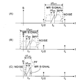
- FIG. 5 is a schematic diagram showing a waveform of an MR signal generated by each signal processing shown in FIG. 4.
- FIG. 9 is a schematic diagram illustrating a frequency band of an MR signal generated by signal processing in the receiver illustrated in FIG.
- FIG. 1 is a configuration diagram of a magnetic resonance imaging apparatus according to the first embodiment of the present invention.
- the magnetic resonance imaging apparatus 20 includes a cylindrical static magnetic field magnet 21 that forms a static magnetic field, a shim coil 22, a gradient magnetic field coil 23, and an RF coil 24 provided inside the static magnetic field magnet 21.
- the magnetic resonance imaging apparatus 20 is provided with a control system 25.
- the control system 25 includes a static magnetic field power supply 26, a gradient magnetic field power supply 27, a shim coil power supply 28, a transmitter 29, a receiver 30, a sequence controller 31, and a computer 32.
- the gradient magnetic field power source 27 of the control system 25 includes an X-axis gradient magnetic field power source 27x, a Y-axis gradient magnetic field power source 27y, and a Z-axis gradient magnetic field power source 27z.
- the computer 32 includes an input device 33, a display device 34, an arithmetic device 35, and a storage device 36.
- the static magnetic field magnet 21 is connected to the static magnetic field power supply 26 and has a function of forming a static magnetic field in the imaging region by a current supplied from the static magnetic field power supply 26.
- the static magnetic field magnet 21 is composed of a superconducting coil, and is connected to the static magnetic field power supply 26 at the time of excitation and supplied with current. It is common.
- the static magnetic field magnet 21 is composed of a permanent magnet and the static magnetic field power supply 26 is not provided.
- a cylindrical shim coil 22 is provided coaxially inside the static magnetic field magnet 21.
- the shim coil 22 is connected to the shim coil power supply 28, and is configured such that a current is supplied from the shim coil power supply 28 to the shim coil 22 to make the static magnetic field uniform.
- the gradient magnetic field coil 23 includes an X-axis gradient magnetic field coil 23x, a Y-axis gradient magnetic field coil 23y, and a Z-axis gradient magnetic field coil 23z, and is formed in a cylindrical shape inside the static magnetic field magnet 21.
- a bed 37 is provided inside the gradient magnetic field coil 23 as an imaging region, and the subject P is set on the bed 37.
- the RF coil 24 includes a whole body coil (WBC: whole body coil) for transmitting and receiving an RF signal built in the gantry, a local coil for receiving RF signals provided in the vicinity of the bed 37 and the subject P, and the like.
- WBC whole body coil
- the gradient magnetic field coil 23 is connected to a gradient magnetic field power source 27.
- the X-axis gradient magnetic field coil 23x, the Y-axis gradient magnetic field coil 23y, and the Z-axis gradient magnetic field coil 23z of the gradient magnetic field coil 23 are respectively an X-axis gradient magnetic field power supply 27x, a Y-axis gradient magnetic field power supply 27y, and a Z-axis gradient magnetic field coil 27z. It is connected to the magnetic field power supply 27z.
- the X-axis gradient magnetic field power source 27x, the Y-axis gradient magnetic field power source 27y, and the Z-axis gradient magnetic field power source 27z are supplied with currents supplied to the X-axis gradient magnetic field coil 23x, the Y-axis gradient magnetic field coil 23y, and the Z-axis gradient magnetic field coil 23z, respectively.
- a gradient magnetic field Gx in the X-axis direction, a gradient magnetic field Gy in the Y-axis direction, and a gradient magnetic field Gz in the Z-axis direction can be formed, respectively.
- the RF coil 24 is connected to at least one of the transmitter 29 and the receiver 30.
- the transmission RF coil 24 has a function of receiving an RF signal from the transmitter 29 and transmitting it to the subject P, and the reception RF coil 24 is accompanied by excitation of the nuclear spin inside the subject P by the RF signal. It has a function of receiving the NMR signal generated in this way and giving it to the receiver 30.
- the sequence controller 31 of the control system 25 is connected to the gradient magnetic field power source 27, the transmitter 29, and the receiver 30.
- the sequence controller 31 is control information necessary for driving the gradient magnetic field power supply 27, the transmitter 29, and the receiver 30, for example, operation control information such as the intensity, application time, and application timing of the pulse current to be applied to the gradient magnetic field power supply 27.
- the gradient magnetic field power supply 27, the transmitter 29 and the receiver 30 are driven according to the stored predetermined sequence to drive the X-axis gradient magnetic field Gx, the Y-axis gradient magnetic field Gy, and the Z-axis gradient magnetic field. It has the function of generating Gz and RF signals.
- sequence controller 31 is configured to receive raw data (raw data) that is complex data obtained by detection of the NMR signal and A / D (analog digital) conversion in the receiver 30 and supply the raw data to the computer 32.
- raw data raw data
- a / D analog digital
- the transmitter 29 is provided with a function of applying an RF signal to the RF coil 24 based on the control information received from the sequence controller 31, while the receiver 30 detects the NMR signal received from the RF coil 24. Then, by executing required signal processing and A / D conversion, a function of generating raw data that is digitized complex data and a function of supplying the generated raw data to the sequence controller 31 are provided.
- the computer 32 is provided with various functions by executing the program stored in the storage device 36 of the computer 32 by the arithmetic unit 35.
- a specific circuit having various functions may be provided in the magnetic resonance imaging apparatus 20 instead of at least a part of the program.
- the computing device 35 of the computer 32 has a function of setting an imaging condition including a pulse sequence and outputting the imaging condition to the sequence controller 31, and a Fourier transform (FT: Fourier transform) to the MR signal output from the sequence controller 31.
- FT Fourier transform
- the computer 32 has a function as an image generation system that generates MR image data based on the MR signal.
- the receiver 30 is configured to sample the MR signal by direct sampling in which the MR signal received by the receiving RF coil 24 is AD converted without frequency conversion.
- FIG. 2 is a functional block diagram showing detailed configurations of the transmitter 29 and the receiver 30 shown in FIG.
- the transmitter 29 includes a crystal resonator 29A, a frequency divider 29B, a DDS 29C, a DA converter (DAC: digital to analog converter) 29D, a waveform envelope creation unit 29E, a mixer 29F, and an amplifier 29G.
- DAC digital to analog converter
- the analog clock signal generated using the crystal oscillator 29A as the original oscillation is frequency-divided into an analog clock signal having a predetermined frequency by the frequency divider 29B.
- a clock signal having a frequency different from the frequency generated by the frequency divider 29B, for example, a higher frequency is generated as a digital signal in the DDS 29C.
- the clock signal generated in the DDS 29C is converted into an analog clock signal in the DAC 29D, and is output to the mixer 29F as a transmission carrier together with the clock signal generated in the frequency divider 29B.
- an analog waveform signal having an envelope created by the waveform envelope creation unit 29 is output to the mixer 29F.
- the waveform signal is frequency-modulated by the transmission carrier by the mixer 29F.
- the modulated waveform signal is amplified by the amplifier 29G as an RF transmission signal and then output to the RF transmission coil 24A.
- the receiver 30 includes an amplifier 30A, a band pass filter (BPF) 30B, an AD converter (ADC) 30C, a down-conversion / IQ separation unit 30D, a digital filter 30E, an up-conversion unit 30F, and IQ.
- a synthesis unit 30G, a bit selector 30H, and a reception detection carrier generation unit 30I are included.
- the reception detection carrier generation unit 30I can further be constituted by a first DDS 30J and a second DDS 30K.
- components that process digital signals can be configured by having a computer read a program, or can be configured by a circuit.
- MR signal received by the RF receiving coil 24B is amplified by the amplifier 30A and input to the BPF 30B.
- the analog MR signal whose frequency band is limited in the BPF 30B is digitally converted in the ADC 30C without being frequency-converted. That is, the receiver 30 executes direct sampling of the MR signal.
- the MR signal after AD conversion is down-converted into a signal having a baseband frequency by the down-conversion / IQ separation unit 30D, and an in-phase (I) signal and a quadrature-phase (Q) signal Separated.
- each reception detection carrier for the I signal and Q signal generated in the reception detection carrier generation unit 30I is output to the down-conversion / IQ separation unit 30D, and the MR signal after AD conversion by the mixer is generated. Demodulated.
- the reception detection carrier generator 30I generates reception detection carriers as digital signals by the first DDS 30J and the second DDS 30K for each frequency.
- a reception detection carrier having the same frequency as the transmission carrier generated in the DDS 29C of the transmitter 29 is generated.
- the second DDS 30K a reception detection carrier having the same frequency as the frequency of the transmission carrier generated in the frequency divider 29B of the transmitter 29 is generated.
- the transmission carrier generated as a digital signal in the DDS 29C of the transmitter 29 does not use the crystal unit 29A as the original oscillation. For this reason, an error occurs in the frequency and phase of the transmission carrier generated in the DDS 29C with respect to the frequency and phase of the transmission carrier on the low frequency side generated as an analog signal in the frequency divider 29B.
- the reception detection carrier on the high frequency side generated in the first DDS 30J is generated as a digital signal by the same method as the transmission carrier generation method in the DDS 29C of the transmitter 29 without using the crystal resonator 29A as the original oscillation.
- the error of the reception detection carrier generated in the first DDS 30J and the error of the transmission carrier generated in the DDS 29C of the transmitter 29 are equal to each other.
- the error of the transmission carrier generated in the DDS 29C is offset by the error of the reception detection carrier generated in the first DDS 30J.
- the first DDS 30J can generate a reception detection carrier at an appropriate timing corresponding to the transmission carrier.
- the reception detection carrier on the low frequency side generated in the second DDS 30K does not use the crystal unit 29A as the original oscillation. For this reason, an error occurs in the frequency and phase of the reception detection carrier generated in the second DDS 30K with respect to the frequency and phase of the transmission carrier generated in the frequency divider 29B.
- the second DDS 30K acquires an analog clock signal from the frequency divider 29B, and based on the acquired clock signal, a frequency and phase error accumulated in the reception detection carrier is corrected. Is reset to an initial value such as zero. Thereby, also in the second DDS 30K, it is possible to generate a carrier for reception detection at an appropriate timing corresponding to the transmission carrier.
- the receiver 30 constituting the MR data collection system has an I signal and a Q corresponding to the RF transmission signal in which the clock of the transmission carrier is generated by a method of dividing the clock generated using the crystal oscillator 29A as the original oscillation.
- Each detection carrier for a signal which is generated by a method of dividing a clock generated by using the crystal oscillator 29A as an original oscillation, a phase error of the clock of each detection carrier for which a clock is generated by a generation method by DDS. It functions as a correction unit that performs correction based on the clock.
- the reception detection carrier generation unit 30I is configured to output the reception detection carrier after phase correction as described above to the down-conversion / IQ separation unit 30D. For this reason, the down-conversion / IQ separation unit 30D performs reception detection of the I signal and the Q signal using the reception detection carrier after phase correction.
- the I signal and Q signal output from the down conversion / IQ separation unit 30D are output to the digital filter 30E.
- filter processing for noise removal is individually performed on the I signal and the Q signal.
- a common filter is used for filtering the I signal and the Q signal.
- a low-pass filter LPF: low pass filter
- FIR finite impulse response
- the filtered I signal and Q signal are up-converted to an intermediate frequency in the up-conversion unit 30F, and then synthesized with each other in the IQ synthesis unit 30G. Then, the MR signal is output from the IQ combining unit 30G to the components such as the sequence controller 31 via the bit selector 30H.
- the receiver 30 constituting the MR signal data collection system in this way includes a conversion unit that converts an analog MR signal received by the RF receiving coil 24B into a digital MR signal without down-conversion, and a digital MR signal.
- a filter processing unit that performs filter processing using a common filter for noise removal on each of the I signal and the Q signal, and a separation unit that separates the I signal and the Q signal down-converted into baseband It has the function of Further, the receiver 30 has a function as a combining unit that combines the filtered I signal and Q signal after up-converting them to a predetermined frequency.
- the subject P is set on the bed 37 in advance, and a static magnetic field is formed in the imaging region of the static magnetic field magnet 21 (superconducting magnet) excited by the static magnetic field power supply 26. Further, a current is supplied from the shim coil power supply 28 to the shim coil 22, and the static magnetic field formed in the imaging region is made uniform.
- an imaging scan of the subject P is executed. That is, the data acquisition system configured by the components of the magnetic resonance imaging apparatus 20 for executing the scan of the sequence controller 31 and the static magnetic field magnet 21 is subject to the imaging conditions including the pulse sequence set in the computer 32. MR signals are collected from the specimen P.
- the sequence controller 31 drives the gradient magnetic field power source 27, the transmitter 29, and the receiver 30 according to the imaging conditions to form a gradient magnetic field in the imaging region where the subject P is set, and performs RF transmission.
- An RF signal is generated from the coil 24A. Therefore, the MR signal generated by the magnetic resonance inside the subject P is received by the RF receiving coil 24 ⁇ / b> B and given to the receiver 30. Then, the receiver 30 executes MR signal detection processing by the direct sampling method.
- the analog MR signal received by the RF receiving coil 24B is amplified by the amplifier 30A and then input to the ADC 30C via the BPF 30B.
- the frequency band of the analog MR signal is limited.
- the frequency band ⁇ f BPF of the BPF 30B is expressed as f s / 2 + ⁇ f MR / where the frequency band of the analog MR signal input to the BPF 30B is ⁇ f MR , the center frequency of the analog MR signal is f 0 , and the sampling frequency is f s.
- FIG. 3 is a diagram showing changes before and after sampling of noise superimposed on the MR signal sampled with the filter processing by the BPF 30B shown in FIG.
- the vertical axis represents the signal amplitude S
- the horizontal axis represents the frequency f.
- 3A shows the MR signal before sampling in the ADC 30C
- FIG. 3B shows the MR signal after sampling in the ADC 30C.
- the filter processing of the BPF 30B provided in the preceding stage of the ADC 30C can prevent an increase in noise floor due to aliasing at the time of undersampling in which the analog MR signal does not satisfy the Nyquist condition with respect to the sampling frequency in the ADC 30C.
- the MR signal AD-converted by the ADC 30C is down-converted by the down-conversion / IQ separation unit 30D and separated into the I signal and the Q signal.
- FIG. 4 is a block diagram showing a flow of signal processing of the MR signal after A / D conversion in the receiver 30 shown in FIG. 1, and FIG. 5 shows an MR signal generated by each signal processing shown in FIG. It is a schematic diagram which shows these waveforms.
- the vertical axis indicates the signal amplitude S
- the horizontal axis indicates the frequency f.
- a dotted line in FIG. 5 indicates a signal generated when it is assumed that the BPF process is not executed before the A / D conversion of the MR signal.
- cos ( ⁇ 0 t) is multiplied by the MR signal S MR.
- -sin ( ⁇ 0 t) is multiplied by the MR signal S MR.
- the I signal and the Q signal generated in the down conversion / IQ separation unit 30D are individually filtered by a common LPF such as an FIR filter in the digital filter 30E.
- a common LPF such as an FIR filter in the digital filter 30E.
- the digital filter 30E if the frequency band of the MR signal to Delta] f MR, it is desirable to perform filtering frequency band of interest as range of Delta] f MR / 2 or Delta] f MR. The reason is that the noise that is turned back by the filter processing can be reduced.
- the number of taps of the digital filter 30 can be reduced by performing the filtering process of the I signal and the Q signal by the decimation filter.
- the decimation filter is an LPF for downsampling with a Nyquist frequency as a cutoff frequency. Even when performing filter processing with a decimation filter, if the sampling frequency after decimation filter processing is f sd , the target frequency band must be in the range of ⁇ f MR / 2 to f sd / 2 Is desirable. Thereby, aliasing noise caused by the decimation filter can be reduced.
- the I signal and Q signal after the filter processing are given to the up-conversion unit 30F.
- the filtered I signal and Q signal are multiplied by cos ( ⁇ IF t) and sin ( ⁇ IF t), respectively.
- the I signal S I_IF cos ( ⁇ IF t + kt) + cos whose frequency is up-converted to an intermediate frequency (IF), respectively.
- ⁇ IF t-kt cos ( ⁇ IF t + kt) + cos ( ⁇ IF t-kt) are generated.
- the I signal S I_IF and the Q signal S Q_IF after up-conversion are combined in the IQ combining unit 30G. Specifically, the up-converted Q signal S Q_IF is subtracted from the up-converted I signal S I_IF . As a result, as shown in FIG.
- FIG. 5 (H) it can be confirmed that a series of signal processing of the MR signal shown in FIG. 4 can generate an up-converted MR signal in which the folded noise is canceled.
- the MR signal after the up-conversion is output to the constituent elements such as the sequence controller 31 via the bit selector 30H.
- the MR signal output from the receiver 30 to the sequence controller 31 is input to the computer 32 through the sequence controller 31. Then, MR image data is reconstructed from the MR signals by image reconstruction processing in the computer 32.
- Each reception detection carrier of the I signal and the Q signal used for down conversion and IQ separation in the down conversion / IQ separation unit 30D described above is generated in the reception detection carrier generation unit 30I.
- the reception detection carrier generation processing in the reception detection carrier generation unit 30I refers to the clock frequency-divided by the frequency divider 29B.
- FIG. 6 is a diagram illustrating a reception detection carrier generation method in the reception detection carrier generation unit 30I illustrated in FIG.
- the first DDS 30J includes a first phase setting unit ⁇ 1, a second phase setting unit ⁇ 2, and each phase setting unit ⁇ 1, ⁇ 2 for generating a reception detection carrier on the high frequency side.
- a corresponding adder is provided.
- the second DDS 30K includes an addition corresponding to the third phase setting unit ⁇ 3, the fourth phase setting unit ⁇ 4, and the phase setting units ⁇ 3 and ⁇ 4 for generating the reception detection carrier on the low frequency side.
- a vessel is provided.
- phase value set in the first phase setting unit ⁇ 1 and the phase value set in the second phase setting unit ⁇ 2 are respectively added by an adder. As a result, phase data on the high frequency side having different frequencies is generated.
- the phase value set in the third phase setting unit ⁇ 3 and the phase value set in the fourth phase setting unit ⁇ 4 are also added by the adders. As a result, phase data on the low frequency side having different frequencies is generated.
- the phase data generated in the first DDS 30J is used as a reception detection carrier corresponding to a transmission carrier generated as a digital signal in the DDS 29C of the transmitter 29 without using the crystal resonator 29A as the original vibration. Further, the reception detection carrier generation method generated in the first DDS 30J is the same as the transmission carrier generation method generated in the DDS 29C of the transmitter 29.
- a reception detection carrier having a frequency corresponding to the frequency of the transmission carrier generated in the frequency divider 29B of the transmitter 29 is generated. Therefore, in the first DDS 30J, a reception detection carrier is generated with the same phase setting value as the phase setting value in the DDS 29C of the transmitter 29.
- the phase data generated in the second DDS 30K is used as a reception detection carrier corresponding to the transmission carrier divided by the frequency divider 29B of the transmitter 29 using the crystal resonator 29A as the original oscillation. Therefore, also in the second DDS 30K, a reception detection carrier having a frequency corresponding to the frequency of the transmission carrier generated in the frequency divider 29B of the transmitter 29 is generated.
- the carrier generation method is different between the frequency divider 29B and the second DDS 30K. For this reason, the phase error between the transmission carrier generated by the frequency divider 29B and the reception detection carrier generated by the second DDS 30K is corrected.
- the clock acquired from the frequency divider 29B is referred to by each adder of the second DDS 30K. Then, the phase data in each adder is reset to zero at a predetermined timing based on the clock acquired from the frequency divider 29B.
- the phase error accumulated by the phase value addition processing in each adder of the second DDS 30K can be reset to zero. Then, it becomes possible to accurately synchronize the phase and frequency of the transmission carrier and the phase and frequency of the carrier for reception detection.
- the period and interval for resetting the phase data can be adjusted to the common divisor of the frequency of the clock acquired from the frequency divider 29B and the frequency of the reception detection carrier to be generated in each adder of the second DDS 30K. .
- the frequency of the clock divided from the original oscillation in the frequency divider 29B is 100 MHz and the frequency of the reception detection carrier to be generated in the second DDS 30K is 2 MHz, the promise of 100 MHz and 2 MHz
- the phase data can be reset with a clock with a frequency such as 2 MHz, 1 MHz, 0.5 MHz, and so on. That is, the phase data can be reset every n (n is a natural number) period instead of every period.
- the reception detection carrier generation unit 30I generates a clock for resetting the phase data generated in the second DDS 30K by dividing the clock generated using the crystal oscillator 29A as the original oscillation. Can do.
- the clock for resetting the phase data is a common divisor between the frequency of the clock generated using the crystal oscillator 29A as the original oscillation and the frequency after correction of the clock of each detection carrier that is the target of phase error correction.
- spurious unnecessary signal component
- SFDR spurious-free dynamic range
- the second DDS 30K the number of bits set so that the influence of spurious generated in each detected carrier after correction by phase error correction can be ignored, and each detected carrier to be corrected for phase error is generated. It is preferable to execute the above phase addition processing. Thereby, it is possible to reduce the error between the frequency of the reception detection carrier generated in the second DDS 30K and the frequency of the transmission carrier generated by frequency division, and to avoid the influence of spurious. As a result, it is possible to ensure SNR (signal to noise) ratio.
- the reception detection carriers for each frequency generated as phase data in the first DDS 30J and the second DDS 30K are combined with each other by addition processing.
- the added phase data is converted into corresponding amplitude data cos ( ⁇ 0 t) by referring to a look-up table (LUT) that associates the phase data with the amplitude data.
- LUT look-up table
- phase data added by the adder is converted into phase data whose phase differs by + 90 ° by the 90 ° hybrid. Then, the phase data whose phase is shifted by + 90 ° is converted into the corresponding amplitude data ⁇ sin ( ⁇ 0 t) by referring to the LUT that associates the phase data with the amplitude data.
- the two amplitude data cos ( ⁇ 0 t) and ⁇ sin ( ⁇ 0 t) generated in the reception detection carrier generation unit 30I and shifted in phase by + 90 ° are respectively received by the I signal and the Q signal.
- the signal is supplied to the down conversion / IQ separation unit 30D as a carrier for detection.
- the phase error caused by the difference in the carrier generation method is corrected to generate the reception detection carrier. It becomes possible to perform reception detection of the I signal and the Q signal.
- the correction of the phase error due to the difference in the carrier generation method is not limited to the reception detection processing of the I signal and the Q signal, but can also be executed in the up-conversion of the detected I signal and Q signal to IF. Is preferred.
- the up-conversion unit 30F functions cos ( ⁇ IF t) and sin ( ⁇ generated respectively by using clocks obtained by dividing the clock generated using the crystal resonator 29A as the original oscillation.
- IF t each frequency of the filtered I signal and Q signal can be up-converted to IF.
- the functions cos ( ⁇ IF t) and sin ( ⁇ IF t) multiplied by the I signal and the Q signal for up-conversion are amplitude data cos ( ⁇ 0 t), which is generated as a carrier for reception detection, Similarly to ⁇ sin ( ⁇ 0 t), it can be generated by resetting the phase error using the clock signal acquired from the frequency divider 29B.
- the magnetic resonance imaging apparatus 20 as described above is a filter for directly A / D converting an analog MR signal without frequency conversion, and separating the MR signal into an I signal and a Q signal to remove noise respectively. The processing is executed.
- the magnetic resonance imaging apparatus 20 is configured to synchronize a carrier for receiving and detecting an MR signal corresponding to a transmission carrier generated by frequency division using a clock generated by frequency division.
- the magnetic resonance imaging apparatus 20 it is possible to remove the folded noise with a simple process and configuration by a signal processing technique in which the MR signal is IQ-separated and then the digital filter process is executed. Specifically, it is possible to prevent noises that are turned back by signal processing such as A / D conversion, down conversion, and digital filter processing from being overlapped by performing down conversion and digital filter processing only once. In addition, it is possible to avoid the necessity of providing a steep BPF for the MR signal before A / D conversion. In addition, since digital filter processing is executed after IQ separation, noise that cannot be removed by BPF can be removed.
- the RF signal transmission carrier and the MR signal reception detection carrier are generated by the same circuit. Therefore, the frequency and phase shift between the transmission carrier and the reception detection carrier did not occur due to factors other than the instability of the original oscillation.
- digitization of MR signal reception is progressing with respect to digitization of RF signal transmission.
- the transmission carrier for the RF signal is generated only by frequency division or by the combined use of DDS and frequency division, while the carrier for reception detection is generated only by DDS so that detection of the MR signal can be processed by a digital signal.
- Dividing is a method of outputting a synchronization signal of frequency f / n from an input signal of frequency f, whereas in DDS, a sine wave is generated by adding the phase for each clock. For this reason, in DDS, errors corresponding to the resolution (number of bits) of the set phase value are accumulated.
- the magnetic resonance imaging apparatus 20 can accurately synchronize the frequency and phase of the transmission / reception carrier even when the generation method of the signal transmission / reception carrier is different.
- the transmission carrier is generated by both frequency division and DDS or only by frequency division
- the reception detection carrier is generated only by DDS
- the phase accumulation error that occurs in the reception detection carrier is reset. can do.
- the synchrony between the transmission carrier and the reception detection carrier can be maintained.
- FIG. 7 is a functional block diagram showing a detailed configuration of a transmitter and a receiver provided in the magnetic resonance imaging apparatus according to the second embodiment of the present invention.
- the magnetic resonance imaging apparatus according to the second embodiment is different from the magnetic resonance imaging apparatus 20 according to the first embodiment in the detailed configuration of the receiver 40 constituting the MR signal data collection system.
- Other configurations and operations of the magnetic resonance imaging apparatus according to the second embodiment are not substantially different from those of the magnetic resonance imaging apparatus 20 according to the first embodiment. For this reason, only the detailed configurations of the transmitter 29 and the receiver 40 are illustrated, and the same components are denoted by the same reference numerals and description thereof is omitted.
- the down-conversion / IQ separation unit 30D converts the MR signal after AD conversion into an intermediate frequency instead of an I signal and a Q signal having a baseband frequency. It is configured to convert into an I signal and a Q signal. That is, the down-conversion / IQ separation unit 30D down-converts the MR signal after AD conversion into an MR signal having a desired frequency.
- the output signal from the digital filter 30E is input to the IQ synthesis unit 30G without passing through the up-conversion unit 30F. That is, since the down-conversion / IQ separation unit 30D down-converts the frequency of the MR signal to a desired frequency suitable for signal processing in the subsequent stage of the receiver 40 instead of the baseband frequency, The I signal and the Q signal are synthesized by the IQ synthesis unit 30G without being up-converted. Accordingly, the receiver 40 functions as a combining unit that combines the filtered I signal and Q signal without up-conversion.
- filter processing is executed using separate filters for the I signal and the Q signal down-converted to a predetermined frequency.
- FIG. 8 is a diagram showing a detailed configuration example of the receiver 40 in the second embodiment shown in FIG. 7 in comparison with a detailed configuration example of the receiver 30 in the first embodiment.
- FIG. 8A shows a detailed configuration example of the receiver 40 in the second embodiment.
- FIG. 8B shows a detailed configuration example of the receiver 30 in the first embodiment.
- the frequency band of the analog MR signal amplified by the amplifier 30A is limited by the BPF 30B.
- the analog MR signal that has passed through the BPF 30B is digitally converted by the ADC 30C without being subjected to frequency conversion. That is, direct sampling of MR signals is executed.
- FIG. 9 is a schematic diagram showing the frequency band of the MR signal generated by the signal processing in the receiver 40 shown in FIG.
- the vertical axis indicates the signal amplitude S
- the horizontal axis indicates the frequency f.
- FIG. 9A shows the frequency band of the MR signal immediately after sampling in the ADC 30C.
- an MR signal having a center frequency of f 0 and a frequency band of ⁇ f MR is sampled at a sampling frequency f s .
- a noise component exists in the frequency band ⁇ f BPF of the BPF 30B.
- the MR signal after AD conversion is down-converted into a signal having an intermediate frequency in the down-conversion / IQ separation unit 30D and separated into an I signal and a Q signal.
- each reception detection carrier for the I signal and the Q signal is multiplied by the MR signal after AD conversion by the mixer.
- the center frequency of the MR signal in which the noise component is superimposed on the frequency band ⁇ f BPF of the BPF 30B becomes the intermediate frequency f IF .
- the strength of the static magnetic field is 1.5 [T]
- a frequency of about 36 [MHz] is down-converted to an intermediate frequency of about 0.5 [MHz].
- the sampling rate is about 100 [MSPS] to 2 [MSPS].
- the intermediate frequency I signal and Q signal generated in the down conversion / IQ separation unit 30D are output to the digital filter 30E.
- the digital filter 30E is a decimation filter
- the digital filter 30E can be expressed by an LPF and a decimation filter, as shown in FIG.
- an LPF and a decimation filter are respectively applied to the I signal and the Q signal.
- a noise component is removed from the I signal and the Q signal. That is, as shown in FIG. 9C, an I signal and a Q signal whose noise components are limited to the LPF frequency band ⁇ f LPF are generated by the LPF that is a complex filter.
- the I signal and Q signal output from the digital filter 30E are synthesized by the IQ synthesis unit 30G without being up-converted. And then.
- the MR signal generated by combining the I signal and the Q signal in the IQ combining unit 30G is output from the receiver 40 via the bit selector 30H.
- the down-conversion / IQ separation unit 30D generates an I signal and a Q signal whose frequency is down-converted to the baseband that is the minimum frequency. For this reason, as shown in FIG. 8B, an up-conversion unit 30F is provided after the digital filter 30E. Then, the filtered I signal and Q signal whose frequency is down-converted to the baseband are up-converted to an intermediate frequency in the up-conversion unit 30F.
- filter processing for noise removal can be executed by separating the I signal and the Q signal by various signal processing variations. As a result, it is possible to prevent noise from being superposed due to down conversion of the MR signal to the intermediate frequency after sampling. In other words, digital filter processing can be performed so that noises do not overlap with each other as the MR signal is down-converted.
- the magnetic resonance imaging apparatus down-converts and separates the MR signal after A / D conversion into an I signal and a Q signal of an intermediate frequency, and separately converts the I signal and the Q signal respectively.
- Filter processing is executed using the above filter.
- the magnetic resonance imaging apparatus in the second embodiment an effect equivalent to that of the magnetic resonance imaging apparatus 20 in the first embodiment can be obtained.
- the configuration and signal processing of the receiver 40 can be simplified.
- the embodiment is not limited to the frequency division, and is generated by a method other than the DDS.
- the phase error between the clock generated by the DDS and the clock generated by the DDS can be reset based on the clock generated by the method other than the DDS.
- the receiver 30 receives each detection carrier for the I signal and the Q signal corresponding to the RF transmission signal in which the clock of the transmission carrier is generated by a method other than the generation method by the DDS among the I signal and the Q signal.
- the receiver 30 uses a detection carrier for MR signals corresponding to an RF transmission signal in which a transmission carrier clock is generated by a method other than the DDS generation method among digital MR signals collected by direct sampling. Therefore, it is possible to provide a function of correcting the phase error of the clock of the detection carrier in which the clock is generated by the DDS generation method based on the clock generated by the method other than the DDS generation method.
- the configuration in which the receiver 30 is connected to the RF receiving coil 24B is illustrated, but the receiver 30 may be integrated with the RF receiving coil 24B.
- the receiver 30 is usually a component of the RF receiving coil 24B.
Landscapes
- Health & Medical Sciences (AREA)
- Physics & Mathematics (AREA)
- Life Sciences & Earth Sciences (AREA)
- Engineering & Computer Science (AREA)
- Condensed Matter Physics & Semiconductors (AREA)
- General Physics & Mathematics (AREA)
- Signal Processing (AREA)
- Nuclear Medicine, Radiotherapy & Molecular Imaging (AREA)
- General Health & Medical Sciences (AREA)
- Animal Behavior & Ethology (AREA)
- Public Health (AREA)
- Biophysics (AREA)
- Pathology (AREA)
- Biomedical Technology (AREA)
- Heart & Thoracic Surgery (AREA)
- Medical Informatics (AREA)
- Molecular Biology (AREA)
- Surgery (AREA)
- Veterinary Medicine (AREA)
- High Energy & Nuclear Physics (AREA)
- Radiology & Medical Imaging (AREA)
- Computer Vision & Pattern Recognition (AREA)
- Physiology (AREA)
- Psychiatry (AREA)
- Artificial Intelligence (AREA)
- Magnetic Resonance Imaging Apparatus (AREA)
Abstract
実施形態に係る磁気共鳴イメージング装置は、データ収集ユニットと画像生成ユニットとを備える。前記データ収集ユニットは、被検体から磁気共鳴信号を収集する。前記画像生成ユニットは、前記磁気共鳴信号に基づいて磁気共鳴画像データを生成する。また、前記データ収集ユニットは、変換部、分離部及びフィルタ処理部を有する。変換部は、高周波コイルで受信されたアナログの前記磁気共鳴信号を、ダウンコンバージョンせずにデジタルの前記磁気共鳴信号に変換する。分離部は、前記デジタルの前記磁気共鳴信号を、同相信号と直交位相信号とに分離する。フィルタ処理部は、前記同相信号及び前記直交位相信号に対してノイズの除去用のフィルタ処理を実行する。
Description
本発明の実施形態は、磁気共鳴イメージング(MRI: Magnetic Resonance Imaging)装置及び磁気共鳴イメージング方法に関する。
MRI装置は、静磁場中に置かれた被検体の原子核スピンをラーモア周波数の高周波(RF: radio frequency)信号で磁気的に励起し、この励起に伴って発生する核磁気共鳴(NMR: nuclear magnetic resonance)信号から画像を再構成する画像診断装置である。
MRI装置では、ダイレクトサンプリング方式によるMR信号の検波処理が提案されている。ダイレクトサンプリング方式は、アナログ信号を、周波数変換を行わずに直接AD (analog to digital)変換して検波する信号処理方式である。MR信号をダイレクトサンプリングする場合には、ダイレクトデジタルシンセサイザ(DDS: direct digital synthesizer)により作成したMR信号の検波用キャリアを用いてデジタル信号の検波が実行される。尚、DDSは、任意の波形や周波数をデジタル的に生成する回路又はシステムである。
MR画像を高品質に生成するためには、MR信号に重畳するノイズ及び誤差を低減させることが重要である。
そこで、本発明は、ダイレクトサンプリング方式によりMR信号を受信する場合において、ノイズや誤差等がより低減されたMR信号を取得することが可能な磁気共鳴イメージング装置及び磁気共鳴イメージング方法を提供することを目的とする。
本発明の実施形態に係る磁気共鳴イメージング装置は、データ収集ユニットと画像生成ユニットとを備える。前記データ収集ユニットは、被検体から磁気共鳴信号を収集する。前記画像生成ユニットは、前記磁気共鳴信号に基づいて磁気共鳴画像データを生成する。また、前記データ収集ユニットは、変換部、分離部及びフィルタ処理部を有する。変換部は、高周波コイルで受信されたアナログの前記磁気共鳴信号を、ダウンコンバージョンせずにデジタルの前記磁気共鳴信号に変換する。分離部は、前記デジタルの前記磁気共鳴信号を、同相信号と直交位相信号とに分離する。フィルタ処理部は、前記同相信号及び前記直交位相信号に対してノイズの除去用のフィルタ処理を実行する。
また、本発明の実施形態に係る磁気共鳴イメージング装置は、データ収集ユニットと画像生成ユニットとを備える。前記データ収集ユニットは、被検体から磁気共鳴信号を収集する。前記画像生成ユニットは、前記磁気共鳴信号に基づいて磁気共鳴画像データを生成する。また、前記データ収集ユニットは、変換部及び補正部を有する。変換部は、高周波コイルで受信されたアナログの前記磁気共鳴信号を、ダウンコンバージョンせずにデジタルの前記磁気共鳴信号に変換する。補正部は、前記デジタルの前記磁気共鳴信号のうち、ダイレクトデジタルシンセサイザによる生成方式以外の方式によって送信キャリアのクロックが生成される高周波送信信号に対応する磁気共鳴信号用の検波キャリアであって前記ダイレクトデジタルシンセサイザによる生成方式でクロックが生成される前記検波キャリアのクロックの位相誤差を、前記ダイレクトデジタルシンセサイザによる生成方式以外の方式で生成されるクロックに基づいて補正する。
また、本発明の実施形態に係る磁気共鳴イメージング方法は、被検体から磁気共鳴信号を収集するステップと、前記磁気共鳴信号に基づいて磁気共鳴画像データを生成するステップとを有する。前記磁気共鳴画像データの生成は、高周波コイルで受信されたアナログの前記磁気共鳴信号を、ダウンコンバージョンせずにデジタルの前記磁気共鳴信号に変換するステップと、前記デジタルの前記磁気共鳴信号を、同相信号と直交位相信号とに分離するステップと、前記同相信号及び前記直交位相信号に対してノイズの除去用のフィルタ処理を実行するステップとを有する。
また、本発明の実施形態に係る磁気共鳴イメージング方法は、被検体から磁気共鳴信号を収集するステップと、前記磁気共鳴信号に基づいて磁気共鳴画像データを生成するステップとを有する。前記磁気共鳴画像データの生成は、高周波コイルで受信されたアナログの前記磁気共鳴信号を、ダウンコンバージョンせずにデジタルの前記磁気共鳴信号に変換するステップと、前記デジタルの前記磁気共鳴信号のうち、ダイレクトデジタルシンセサイザによる生成方式以外の方式によって送信キャリアのクロックが生成される高周波送信信号に対応する磁気共鳴信号用の検波キャリアであって前記ダイレクトデジタルシンセサイザによる生成方式でクロックが生成される前記検波キャリアのクロックの位相誤差を、前記ダイレクトデジタルシンセサイザによる生成方式以外の方式で生成されるクロックに基づいて補正するステップとを有する。
また、本発明の実施形態に係る磁気共鳴イメージング装置は、データ収集ユニットと画像生成ユニットとを備える。前記データ収集ユニットは、被検体から磁気共鳴信号を収集する。前記画像生成ユニットは、前記磁気共鳴信号に基づいて磁気共鳴画像データを生成する。また、前記データ収集ユニットは、変換部及び補正部を有する。変換部は、高周波コイルで受信されたアナログの前記磁気共鳴信号を、ダウンコンバージョンせずにデジタルの前記磁気共鳴信号に変換する。補正部は、前記デジタルの前記磁気共鳴信号のうち、ダイレクトデジタルシンセサイザによる生成方式以外の方式によって送信キャリアのクロックが生成される高周波送信信号に対応する磁気共鳴信号用の検波キャリアであって前記ダイレクトデジタルシンセサイザによる生成方式でクロックが生成される前記検波キャリアのクロックの位相誤差を、前記ダイレクトデジタルシンセサイザによる生成方式以外の方式で生成されるクロックに基づいて補正する。
また、本発明の実施形態に係る磁気共鳴イメージング方法は、被検体から磁気共鳴信号を収集するステップと、前記磁気共鳴信号に基づいて磁気共鳴画像データを生成するステップとを有する。前記磁気共鳴画像データの生成は、高周波コイルで受信されたアナログの前記磁気共鳴信号を、ダウンコンバージョンせずにデジタルの前記磁気共鳴信号に変換するステップと、前記デジタルの前記磁気共鳴信号を、同相信号と直交位相信号とに分離するステップと、前記同相信号及び前記直交位相信号に対してノイズの除去用のフィルタ処理を実行するステップとを有する。
また、本発明の実施形態に係る磁気共鳴イメージング方法は、被検体から磁気共鳴信号を収集するステップと、前記磁気共鳴信号に基づいて磁気共鳴画像データを生成するステップとを有する。前記磁気共鳴画像データの生成は、高周波コイルで受信されたアナログの前記磁気共鳴信号を、ダウンコンバージョンせずにデジタルの前記磁気共鳴信号に変換するステップと、前記デジタルの前記磁気共鳴信号のうち、ダイレクトデジタルシンセサイザによる生成方式以外の方式によって送信キャリアのクロックが生成される高周波送信信号に対応する磁気共鳴信号用の検波キャリアであって前記ダイレクトデジタルシンセサイザによる生成方式でクロックが生成される前記検波キャリアのクロックの位相誤差を、前記ダイレクトデジタルシンセサイザによる生成方式以外の方式で生成されるクロックに基づいて補正するステップとを有する。
本発明の実施形態に係る磁気共鳴イメージング装置及び磁気共鳴イメージング方法について添付図面を参照して説明する。
(第1の実施形態)
図1は本発明の第1の実施形態に係る磁気共鳴イメージング装置の構成図である。
図1は本発明の第1の実施形態に係る磁気共鳴イメージング装置の構成図である。
磁気共鳴イメージング装置20は、静磁場を形成する筒状の静磁場用磁石21、この静磁場用磁石21の内側に設けられたシムコイル22、傾斜磁場コイル23及びRFコイル24を備えている。
また、磁気共鳴イメージング装置20には、制御系25が備えられる。制御系25は、静磁場電源26、傾斜磁場電源27、シムコイル電源28、送信器29、受信器30、シーケンスコントローラ31及びコンピュータ32を具備している。制御系25の傾斜磁場電源27は、X軸傾斜磁場電源27x、Y軸傾斜磁場電源27y及びZ軸傾斜磁場電源27zで構成される。また、コンピュータ32には、入力装置33、表示装置34、演算装置35及び記憶装置36が備えられる。
静磁場用磁石21は静磁場電源26と接続され、静磁場電源26から供給された電流により撮像領域に静磁場を形成させる機能を有する。尚、静磁場用磁石21は超伝導コイルで構成される場合が多く、励磁の際に静磁場電源26と接続されて電流が供給されるが、一旦励磁された後は非接続状態とされるのが一般的である。また、静磁場用磁石21を永久磁石で構成し、静磁場電源26が設けられない場合もある。
また、静磁場用磁石21の内側には、同軸上に筒状のシムコイル22が設けられる。シムコイル22はシムコイル電源28と接続され、シムコイル電源28からシムコイル22に電流が供給されて静磁場が均一化されるように構成される。
傾斜磁場コイル23は、X軸傾斜磁場コイル23x、Y軸傾斜磁場コイル23y及びZ軸傾斜磁場コイル23zで構成され、静磁場用磁石21の内側において筒状に形成される。傾斜磁場コイル23の内側には寝台37が設けられて撮像領域とされ、寝台37には被検体Pがセットされる。RFコイル24にはガントリに内蔵されたRF信号の送受信用の全身用コイル(WBC: whole body coil)や寝台37や被検体P近傍に設けられるRF信号の受信用の局所コイルなどがある。
また、傾斜磁場コイル23は、傾斜磁場電源27と接続される。傾斜磁場コイル23のX軸傾斜磁場コイル23x、Y軸傾斜磁場コイル23y及びZ軸傾斜磁場コイル23zはそれぞれ、傾斜磁場電源27のX軸傾斜磁場電源27x、Y軸傾斜磁場電源27y及びZ軸傾斜磁場電源27zと接続される。
そして、X軸傾斜磁場電源27x、Y軸傾斜磁場電源27y及びZ軸傾斜磁場電源27zからそれぞれX軸傾斜磁場コイル23x、Y軸傾斜磁場コイル23y及びZ軸傾斜磁場コイル23zに供給された電流により、撮像領域にそれぞれX軸方向の傾斜磁場Gx、Y軸方向の傾斜磁場Gy、Z軸方向の傾斜磁場Gzを形成することができるように構成される。
RFコイル24は、送信器29及び受信器30の少なくとも一方と接続される。送信用のRFコイル24は、送信器29からRF信号を受けて被検体Pに送信する機能を有し、受信用のRFコイル24は、被検体P内部の原子核スピンのRF信号による励起に伴って発生したNMR信号を受信して受信器30に与える機能を有する。
一方、制御系25のシーケンスコントローラ31は、傾斜磁場電源27、送信器29及び受信器30と接続される。シーケンスコントローラ31は傾斜磁場電源27、送信器29及び受信器30を駆動させるために必要な制御情報、例えば傾斜磁場電源27に印加すべきパルス電流の強度や印加時間、印加タイミング等の動作制御情報を記述したシーケンス情報を記憶する機能と、記憶した所定のシーケンスに従って傾斜磁場電源27、送信器29及び受信器30を駆動させることによりX軸傾斜磁場Gx、Y軸傾斜磁場Gy,Z軸傾斜磁場Gz及びRF信号を発生させる機能を有する。
また、シーケンスコントローラ31は、受信器30におけるNMR信号の検波及びA/D (analog to digital)変換により得られた複素データである生データ(raw data)を受けてコンピュータ32に与えるように構成される。
このため、送信器29には、シーケンスコントローラ31から受けた制御情報に基づいてRF信号をRFコイル24に与える機能が備えられる一方、受信器30には、RFコイル24から受けたNMR信号を検波して所要の信号処理を実行するとともにA/D変換することにより、デジタル化された複素データである生データを生成する機能と生成した生データをシーケンスコントローラ31に与える機能とが備えられる。
また、コンピュータ32の記憶装置36に保存されたプログラムを演算装置35で実行することにより、コンピュータ32には各種機能が備えられる。ただし、プログラムの少なくとも一部に代えて、各種機能を有する特定の回路を磁気共鳴イメージング装置20に設けてもよい。
具体的には、コンピュータ32の演算装置35には、パルスシーケンスを含む撮像条件を設定してシーケンスコントローラ31に出力する機能、シーケンスコントローラ31から出力されたMR信号にフーリエ変換(FT: Fourier transform)を含む画像再構成処理を施すことによってMR画像データを生成する機能、MR画像データに様々な画像処理を施す機能が備えられる。すなわち、コンピュータ32は、MR信号に基づいてMR画像データを生成する画像生成システムとしての機能を有している。
次に、受信器30の詳細構成及び詳細機能について説明する。受信器30は受信用のRFコイル24により受信されたMR信号を周波数変換せずにAD変換するダイレクトサンプリングによってMR信号のサンプリングを行うように構成されている。
図2は、図1に示す送信器29及び受信器30の詳細構成を示す機能ブロック図である。
送信器29は、水晶振動子29A、分周器29B、DDS29C、DAコンバータ(DAC: digital to analog converter)29D、波形エンベロープ作成部29E、ミキサ29F及びアンプ29Gを有する。
水晶振動子29Aを原振として生成されるアナログのクロック信号は、分周器29Bにおいて所定の周波数を有するアナログのクロック信号に分周される。一方、分周器29Bにより生成される周波数と異なる周波数、例えばより高い周波数のクロック信号がDDS29Cにおいてデジタル信号として生成される。DDS29Cにおいて生成されたクロック信号は、DAC29Dにおいてアナログのクロック信号に変換され、分周器29Bで生成されるクロック信号とともに送信キャリアとしてミキサ29Fに出力される。
一方、波形エンベロープ作成部29において作成された包絡線を有するアナログの波形信号がミキサ29Fに出力される。これにより、波形信号がミキサ29Fで送信キャリアにより周波数変調される。変調された波形信号はRF送信信号としてアンプ29Gで増幅された後、RF送信コイル24Aに出力される。
他方、受信器30は、アンプ30A、バンドパスフィルタ(BPF: band pass filter)30B、ADコンバータ(ADC; AD converter)30C、ダウンコンバージョン・IQ分離部30D、デジタルフィルタ30E、アップコンバート部30F、IQ合成部30G、ビットセレクタ30H及び受信検波用キャリア生成部30Iを有する。受信検波用キャリア生成部30Iは、更に第1のDDS30J及び第2のDDS30Kで構成することができる。受信器30を構成するこれらの構成要素のうち、デジタル信号を処理する構成要素は、コンピュータにプログラムを読込ませて構成するか或いは回路によって構成することができる。
RF受信コイル24Bにより受信されたMR信号は、アンプ30Aで増幅されてBPF30Bに入力する。BPF30Bにおいて周波数帯域が制限されたアナログのMR信号は周波数変換されることなくADC30Cにおいてデジタル変換される。すなわち、受信器30では、MR信号のダイレクトサンプリングが実行される。
AD変換後のMR信号は、ダウンコンバージョン・IQ分離部30Dにおいてベースバンドの周波数を有する信号にダウンコンバージョンされ、かつ同相(I: in-phase)信号と直交位相(Q: quadrature-phase)信号とに分離される。具体的には、受信検波用キャリア生成部30Iにおいて生成されるI信号及びQ信号用の各受信検波用のキャリアがダウンコンバージョン・IQ分離部30Dに出力され、ミキサによりAD変換後のMR信号が復調される。
受信検波用キャリア生成部30Iでは、周波数別に、第1のDDS30J及び第2のDDS30Kによりデジタル信号として受信検波用キャリアが生成される。第1のDDS30Jでは、送信器29のDDS29Cにおいて生成される送信キャリアの周波数と同一の周波数を有する受信検波用キャリアが生成される。一方、第2のDDS30Kでは、送信器29の分周器29Bにおいて生成される送信キャリアの周波数と同一の周波数を有する受信検波用キャリアが生成される。
送信器29のDDS29Cにおいてデジタル信号として生成される送信キャリアは、水晶振動子29Aを原振としていない。このため、DDS29Cにおいて生成される送信キャリアの周波数及び位相には、分周器29Bにおいてアナログ信号として生成される低周波側の送信キャリアの周波数及び位相に対して誤差が生じる。
しかし、第1のDDS30Jにおいて生成される高周波側の受信検波用キャリアは、送信器29のDDS29Cにおける送信キャリアの生成方法と同一の方法で水晶振動子29Aを原振とせずにデジタル信号として生成される。従って、第1のDDS30Jにおいて生成される受信検波用キャリアの誤差と、送信器29のDDS29Cにおいて生成される送信キャリアの誤差とは、互いに同等となる。このため、DDS29Cにおいて生成される送信キャリアの誤差は、第1のDDS30Jにおいて生成される受信検波用キャリアの誤差によって相殺される。その結果、第1のDDS30Jでは、送信キャリアに対応する適切なタイミングで受信検波用キャリアを生成することができる。
一方、第2のDDS30Kにおいて生成される低周波側の受信検波用キャリアも、水晶振動子29Aを原振としていない。このため、第2のDDS30Kにおいて生成される受信検波用キャリアの周波数及び位相には、分周器29Bにおいて生成される送信キャリアの周波数及び位相に対して誤差が生じる。
そこで、第2のDDS30Kは、分周器29Bからアナログのクロック信号を取得し、取得したクロック信号に基づいて受信検波用キャリアに累積する周波数及び位相の誤差が補正されるように受信検波用キャリアの位相をゼロ等の初期値にリセットするように構成される。これにより、第2のDDS30Kにおいても、送信キャリアに対応する適切なタイミングで受信検波用キャリアを生成することが可能となる。
つまり、MRデータ収集系を構成する受信器30は、水晶振動子29Aを原振として生成されるクロックを分周する方式によって送信キャリアのクロックが生成されるRF送信信号に対応するI信号及びQ信号用の各検波キャリアであってDDSによる生成方式でクロックが生成される各検波キャリアのクロックの位相誤差を、水晶振動子29Aを原振として生成されるクロックを分周する方式で生成されるクロックに基づいてそれぞれ補正する補正部として機能する。
そして、受信検波用キャリア生成部30Iは、上述したような位相補正後の受信検波用キャリアをダウンコンバージョン・IQ分離部30Dに出力するように構成されている。このため、ダウンコンバージョン・IQ分離部30Dでは、位相補正後の受信検波用キャリアを用いてI信号及びQ信号の受信検波が実行される。
ダウンコンバージョン・IQ分離部30Dから出力されるI信号及びQ信号は、デジタルフィルタ30Eに出力される。デジタルフィルタ30Eでは、I信号及びQ信号に対して個別にノイズ除去のためのフィルタ処理が施される。このI信号及びQ信号のフィルタ処理には、共通のフィルタが用いられる。具体例として、フィルタ処理には、有限インパルス応答(FIR: finite impulse response)フィルタ等のローパスフィルタ (LPF: low pass filter)を用いることができる。
フィルタ処理後のI信号及びQ信号は、アップコンバート部30Fにおいて中間周波数にアップコンバージョンされた後、IQ合成部30Gにおいて互いに合成される。そして、IQ合成部30GからMR信号が、ビットセレクタ30Hを経由してシーケンスコントローラ31等の構成要素に出力される。
このようにMR信号のデータ収集系を構成する受信器30は、RF受信コイル24Bで受信されたアナログのMR信号を、ダウンコンバージョンせずにデジタルのMR信号に変換する変換部、デジタルのMR信号を、ベースバンドにダウンコンバージョンされたI信号とQ信号とに分離する分離部並びにI信号及びQ信号に対してそれぞれノイズの除去用の共通のフィルタを用いてフィルタ処理を実行するフィルタ処理部としての機能を有している。更に、受信器30は、フィルタ処理後のI信号とQ信号とを所定の周波数にアップコンバージョンした後に合成する合成部としての機能を有している。
次に磁気共鳴イメージング装置20の動作及び作用について説明する。
まず予め寝台37に被検体Pがセットされ、静磁場電源26により励磁された静磁場用磁石21(超伝導磁石)の撮像領域に静磁場が形成される。また、シムコイル電源28からシムコイル22に電流が供給されて撮像領域に形成された静磁場が均一化される。
そして、被検体Pのイメージングスキャンが実行される。すなわち、シーケンスコントローラ31や静磁場用磁石21等のスキャンを実行するための磁気共鳴イメージング装置20の構成要素で構成されるデータ収集系は、コンピュータ32において設定されたパルスシーケンスを含む撮像条件に従って被検体PからMR信号を収集する。
より具体的には、シーケンスコントローラ31は、撮像条件に従って傾斜磁場電源27、送信器29及び受信器30を駆動させることにより被検体Pがセットされた撮像領域に傾斜磁場を形成させるとともに、RF送信コイル24AからRF信号を発生させる。このため、被検体Pの内部における磁気共鳴により生じたMR信号が、RF受信コイル24Bにより受信されて受信器30に与えられる。そして、受信器30では、ダイレクトサンプリング方式によるMR信号の検波処理が実行される。
具体的には、RF受信コイル24Bにより受信されたアナログのMR信号は、アンプ30Aで増幅された後、BPF30Bを経由してADC30Cに入力する。BPF30Bでは、アナログのMR信号の周波数帯域が制限される。BPF30Bの周波数帯域ΔfBPFは、BPF30Bに入力させるアナログのMR信号の周波数帯域をΔfMR、アナログのMR信号の中心周波数をf0、サンプリング周波数をfsとすると、fs/2+ΔfMR/4<f0<fs-ΔfMR/4の条件において、ΔfBPF<4fs-4f0-ΔfMRかつΔfBPF<4f0-2fs-ΔfMRとなるように設定される。
図3は、図2に示すBPF30Bによるフィルタ処理を伴ってサンプリングされるMR信号に重畳するノイズのサンプリング前後における変化を示す図である。
図3(A)及び(B)において縦軸は信号の振幅Sを示し、横軸は周波数fを示す。また、図3(A)はADC30Cにおけるサンプリング前のMR信号を示し、図3(B)はADC30Cにおけるサンプリング後のMR信号を示す。
図3(A)に示すように中心周波数がf0で周波数帯域がΔfMRのアナログのMR信号をサンプリング周波数fsでサンプリングする場合にfs/2+ΔfMR/4<f0<fs-ΔfMR/4の条件において周波数帯域ΔfBPFがΔfBPF<4fs-4f0-ΔfMRかつΔfBPF<4f0-2fs-ΔfMRとなるBPF30BでMR信号のフィルタ処理を実行すると、ノイズの周波数帯域が、BPF30Bの周波数帯域ΔfBPFに制限される。
このため、図3(B)に示すように、ノイズがナイキスト周波数fs/2で折り返って増幅されたとしても、周波数帯域がΔfMRで中心周波数がfs-f0となったMR信号に折り返ったノイズが重畳することを回避することができる。つまり、ADC30Cの前段に設けられるBPF30Bのフィルタ処理によって、ADC30Cにおけるサンプリング周波数に対してアナログのMR信号がナイキストの条件を満たさないアンダーサンプリング時における折返しによるノイズフロアの増加を防ぐことができる。
ADC30CにおいてAD変換されたMR信号は、ダウンコンバージョン・IQ分離部30Dにおいてダウンコンバージョンされ、かつI信号とQ信号とに分離される。
図4は、図1に示す受信器30におけるA/D変換後のMR信号の信号処理の流れを示すブロック線図であり、図5は、図4に示す各信号処理によって生成されるMR信号の波形を示す模式図である。
尚、図5の各グラフにおいて縦軸は信号の振幅Sを示し、横軸は周波数fを示す。また、図5中の点線は、MR信号のA/D変換前にBPF処理が実行されないと仮定した場合に生じる信号を示す。
図5(A)に示すように±ω0の受信帯域で受信されたMR信号からBPF30Bで抽出されたMR信号SMR=cos(ω0t+kt)がA/D変換の対象となる。但し、kは係数、tは時間である。従って、図4に示すようにデジタル化されたMR信号SMR=cos(ω0t+kt)がダウンコンバージョン・IQ分離部30Dに与えられる。
ダウンコンバージョン・IQ分離部30Dでは、MR信号SMRにcos(ω0t)が乗じられる。これにより、図5(B)に示すように周波数がベースバンドまでダウンコンバートされたI信号SI=cos(ω0t+kt)×cos(ω0t)=cos(2ω0t+kt)+cos(kt)が生成される。加えて、MR信号SMRに-sin(ω0t)が乗じられる。これにより、図5(C)に示すように周波数がベースバンドまでダウンコンバートされたQ信号SQ=cos(ω0t+kt)×-sin(ω0t)=-sin(2ω0t+kt)+sin(kt)が生成される。
次に、ダウンコンバージョン・IQ分離部30Dにおいて生成されたI信号及びQ信号は、デジタルフィルタ30Eにおいて、それぞれ個別にFIRフィルタ等の共通のLPFでフィルタ処理される。フィルタ処理の結果、それぞれ図5(D)及び図5(E)に示すように、周波数がベースバンドに制限されたI信号及びQ信号が得られる。
デジタルフィルタ30Eでは、MR信号の周波数帯域をΔfMRとすると、対象となる周波数帯域をΔfMR/2以上ΔfMR以下の範囲としてフィルタ処理を実行することが望ましい。その理由は、フィルタ処理によって折り返されるノイズを低減することができるためである。
また、デシメーション(decimation)フィルタでI信号及びQ信号のフィルタ処理を実行することにより、デジタルフィルタ30のタップ数を少なくすることができる。尚、デシメーションフィルタは、ナイキスト周波数を遮断周波数とするダウンサンプリング用のLPFである。デシメーションフィルタでフィルタ処理を実行する場合においても、デシメーションフィルタ処理後におけるサンプリング周波数をfsdとすると、対象となる周波数帯域をΔfMR/2以上fsd/2以下の範囲としてフィルタ処理を実行することが望ましい。これにより、デシメーションフィルタによって生じる折り返しノイズを低減することができる。
フィルタ処理後のI信号及びQ信号は、アップコンバート部30Fに与えられる。アップコンバート部30Fでは、フィルタ処理後のI信号及びQ信号にそれぞれcos(ωIFt)及びsin(ωIFt)が乗じられる。これにより、図5(F)及び図5(G)に示すように、それぞれ周波数が中間周波数(IF: Intermediate Frequency)にアップコンバートされたI信号SI_IF=cos(ωIFt+kt)+cos(ωIFt-kt)及びQ信号SQ_IF=-cos(ωIFt+kt)+cos(ωIFt-kt)が生成される。
アップコンバート後のI信号SI_IF及びQ信号SQ_IFは、IQ合成部30Gにおいて合成される。具体的には、アップコンバート後のI信号SI_IFからアップコンバート後のQ信号SQ_IFが減算される。これにより、図5(H)に示すように、I信号SI_IFとQ信号SQ_IFとを成分として合成したアップコンバート後のMR信号SMR_IF=cos(ωIFt+kt)+cos(ωIFt-kt)-{-cos(ωIFt+kt)+cos(ωIFt-kt)}=cos(ωIFt+kt)が生成される。
図5(H)に示すように、図4に示すMR信号の一連の信号処理によって、折り返されたノイズがキャンセルされたアップコンバート後のMR信号を生成できることが確認できる。アップコンバート後のMR信号は、ビットセレクタ30Hを経由してシーケンスコントローラ31等の構成要素に出力される。
受信器30からシーケンスコントローラ31に出力されたMR信号は、シーケンスコントローラ31を通じてコンピュータ32に入力する。そして、コンピュータ32における画像再構成処理によってMR信号からMR画像データが再構成される。
上述したダウンコンバージョン・IQ分離部30Dにおけるダウンコンバージョン及びIQ分離に使用されるI信号及びQ信号の各受信検波用キャリアは、受信検波用キャリア生成部30Iにおいて生成される。受信検波用キャリア生成部30Iにおける受信検波用キャリアの生成処理には、分周器29Bにおいて分周されたクロックが参照される。
図6は、図2に示す受信検波用キャリア生成部30Iにおける受信検波用キャリアの生成方法を示す図である。
図6に示すように、第1のDDS30Jには、高周波側の受信検波用キャリアを生成するための第1の位相設定部Φ1、第2の位相設定部Φ2及び各位相設定部Φ1, Φ2に対応する加算器が備えられる。同様に、第2のDDS30Kには、低周波側の受信検波用キャリアを生成するための第3の位相設定部Φ3、第4の位相設定部Φ4及び各位相設定部Φ3, Φ4に対応する加算器が備えられる。
第1の位相設定部Φ1において設定された位相値及び第2の位相設定部Φ2において設定された位相値は、それぞれ加算器で加算される。これにより、互いに周波数が異なる高周波側の位相データが生成される。同様に、第3の位相設定部Φ3において設定された位相値及び第4の位相設定部Φ4において設定された位相値も、それぞれ加算器で加算される。これにより、互いに周波数が異なる低周波側の位相データが生成される。
第1のDDS30Jにおいて生成される位相データは、送信器29のDDS29Cにおいて水晶振動子29Aを原振とせずにデジタル信号として生成される送信キャリアに対応する受信検波用キャリアとして使用される。また、第1のDDS30Jにおいて生成される受信検波用キャリアの生成方式は、送信器29のDDS29Cにおいて生成される送信キャリアの生成方式と同一である。
従って、第1のDDS30Jでは、送信器29の分周器29Bにおいて生成される送信キャリアの周波数に対応する周波数の受信検波用キャリアが生成される。そのために、第1のDDS30Jでは、送信器29のDDS29Cにおける位相設定値と同一の位相設定値で受信検波用キャリアが生成される。
一方、第2のDDS30Kにおいて生成される位相データは、送信器29の分周器29Bにおいて水晶振動子29Aを原振として分周された送信キャリアに対応する受信検波用キャリアとして使用される。従って、第2のDDS30Kにおいても、送信器29の分周器29Bにおいて生成される送信キャリアの周波数に対応する周波数の受信検波用キャリアが生成される。
但し、分周器29Bと第2のDDS30Kとではキャリアの生成方法が異なる。このため、分周器29Bで生成された送信キャリアと第2のDDS30Kで生成された受信検波用キャリアとの間における位相誤差が補正される。具体的には、分周器29Bから取得されたクロックが第2のDDS30Kの各加算器で参照される。そして、分周器29Bから取得されたクロックに基づく所定のタイミングにおいて各加算器における位相データがゼロにリセットされる。これにより、第2のDDS30Kの各加算器における位相値の加算処理によって蓄積される位相誤差をゼロにリセットすることができる。そして、送信キャリアの位相及び周波数と受信検波用キャリアの位相及び周波数とを正確に同期させることが可能となる。
位相データをリセットする周期及び間隔は、分周器29Bから取得されるクロックの周波数と、第2のDDS30Kの各加算器において生成すべき受信検波用キャリアの周波数との公約数に合わせることができる。具体例として、分周器29Bにおいて原振から分周されたクロックの周波数が100MHzであり、第2のDDS30Kにおいて生成すべき受信検波用キャリアの周波数が2MHzであれば、100MHzと2MHzとの公約数である2MHz、1MHz、0.5MHz、...といった周波数のクロックで位相データのリセットを行うことができる。つまり、位相データは、1周期ごとに限らず、n(nは自然数)周期ごとにリセットすることができる。
このように、受信検波用キャリア生成部30Iでは、第2のDDS30Kにおいて生成される位相データをリセットするためのクロックを、水晶振動子29Aを原振として生成されるクロックの分周によって生成することができる。その場合、位相データをリセットするためのクロックは、水晶振動子29Aを原振として生成されるクロックの周波数と、位相誤差の補正対象となる各検波キャリアのクロックの補正後の周波数との公約数に相当する周波数を有するクロックとすることができる。そして、分周によって生成されたクロックに基づいて位相誤差の補正対象となる各検波キャリアの位相誤差をそれぞれ補正することができる。
尚、第2のDDS30Kの各加算器において蓄積される位相誤差のリセットによってスプリアス(不要な信号成分)が発生する。この結果、スプリアスフリーダイナミックレンジ(SFDR: spurious-free dynamic range)が小さくなる。そこで、スプリアスの影響を低減させるために、第2のDDS30Kの各加算器における位相加算処理のビット数を十分に確保することが望ましい。
つまり、第2のDDS30Kでは、位相誤差の補正によって補正後の各検波キャリアに生じるスプリアスの影響が無視できるように設定されたビット数で、位相誤差の補正対象となる各検波キャリアの生成のための位相加算処理を実行することが好適である。これにより、第2のDDS30Kにおいて生成される受信検波用キャリアの周波数と、分周によって生成される送信キャリアの周波数との間における誤差を低減しつつ、スプリアスの影響も回避することができる。その結果、SNR (signal to noise ratio)を確保することができる。
第1のDDS30J及び第2のDDS30Kにおいてそれぞれ位相データとして生成された周波数別の受信検波用キャリアは、互いに加算処理によって合成される。加算された位相データは、位相データと振幅データとを関連付けた参照テーブル(LUT: look-up table)を参照することによって、対応する振幅データcos(ω0t)に変換される。
一方、加算器で加算された位相データは、90°ハイブリッドにより位相が+90°異なる位相データに変換される。そして、位相が+90°シフトされた位相データは、位相データと振幅データとを関連付けたLUTを参照することによって、対応する振幅データ-sin(ω0t)に変換される。
そして、受信検波用キャリア生成部30Iにおいて生成された、互いに位相が+90°シフトした2つの振幅データcos(ω0t), -sin(ω0t)は、それぞれI信号及びQ信号の受信検波用のキャリアとしてダウンコンバージョン・IQ分離部30Dに与えられる。このように、受信検波用キャリアの生成方式が送信キャリアの生成方式と異なる場合に、キャリアの生成方式の相違に起因する位相誤差を補正して受信検波用キャリアを生成することにより、より適切なI信号及びQ信号の受信検波を行うことが可能となる。
尚、キャリアの生成方式の相違に起因する位相誤差の補正は、I信号及びQ信号の受信検波処理に限らず、検波後のI信号及びQ信号のIFへのアップコンバージョンにおいても実行することが好適である。
より具体的には、アップコンバート部30Fにおいて、水晶振動子29Aを原振として生成されるクロックを分周して得られるクロックを用いてそれぞれ生成される関数cos(ωIFt), sin(ωIFt)を掛けることによって、フィルタ処理後のI信号及びQ信号の各周波数をIFにアップコンバージョンすることができる。その場合、アップコンバージョンのためにI信号及びQ信号に乗じられる関数cos(ωIFt), sin(ωIFt)は、受信検波用のキャリアとして生成される振幅データcos(ω0t), -sin(ω0t)と同様に、分周器29Bから取得されるクロック信号を用いて位相誤差をリセットすることにより生成することができる。
以上のような磁気共鳴イメージング装置20は、アナログのMR信号を周波数変換せずに直接A/D変換し、かつMR信号をI信号とQ信号とに分離してそれぞれノイズを除去するためのフィルタ処理を実行するようにしたものである。また、磁気共鳴イメージング装置20は、分周で生成される送信キャリアに対応するMR信号を受信検波するためのキャリアを、分周によって生成されるクロックを用いて同期させるようにしたものである。
従来の磁気共鳴イメージング装置では、MR信号のダイレクトサンプリングを行おうとすると、A/D変換、ダウンコンバージョン及びデジタルフィルタ処理等の信号処理によってノイズが折り返るという問題があった。折り返ったノイズを低減させるためには、A/D変換前のMR信号に急峻なBPFを掛けるという方法が考えられる。或いは、A/D変換後におけるMR信号のダウンコンバージョンとデジタルフィルタ処理とを交互又は同時に2~3回繰り返すという方法も考えられる。
しかしながら、BPFの特性を急峻にするためには複数のフィルタを多段階に重ねる必要がある。このため、BPFのサイズが大きくなり、MR信号の受信チャンネルの多チャンネル化の障害となる。しかも、BPFのコストの増加に繋がる。従って、BPFの特性を急峻にすることは実用性に欠ける。
一方、MR信号のダウンコンバージョンとデジタルフィルタ処理とを繰返すためには、多くのデジタル処理のための大規模な回路が必要となる。従って、この場合も、回路のサイズ及びコストの増加に繋がることになる。
これに対して、磁気共鳴イメージング装置20によれば、MR信号をIQ分離してからデジタルフィルタ処理を実行するという信号処理手法によって簡易な処理及び構成で折り返ったノイズを除去することができる。具体的には、ダウンコンバージョン及びデジタルフィルタ処理を1回実行するのみで、A/D変換、ダウンコンバージョン及びデジタルフィルタ処理等の信号処理によって折り返ったノイズが重ならないようにすることができる。また、A/D変換前におけるMR信号用に急峻なBPFを設ける必要性も回避することができる。加えて、IQ分離してからデジタルフィルタ処理が実行されるため、BPFにより除去することができないノイズを除去することができる。
また、MR信号のダイレクトサンプリングを行わない従来の磁気共鳴イメージング装置では、RF信号の送信キャリアとMR信号の受信検波用キャリアとが同一の回路で生成されていた。従って、送信キャリアと受信検波用キャリアとの間における周波数及び位相のずれは、原振の不安定性以外の要因では発生しなかった。
しかしながら、送信キャリアと受信検波用キャリアとが異なる方式で生成される場合には、送信キャリアと受信検波用キャリアとの間において周波数及び位相のずれが生じる。すなわち、原振の不安定性のみならず、生成方法の相違を要因として送信キャリアと受信検波用キャリアとの間に周波数及び位相のずれが生じる。
特に、近年の磁気共鳴イメージング装置では、MR信号の受信のデジタル化がRF信号の送信のデジタル化に対して進んでいる。この場合、RF信号用の送信キャリアは分周のみ或いはDDSと分周の併用によって生成される一方、MR信号の検波をデジタル信号で処理できるように、受信検波用キャリアがDDSのみで生成されることとなり得る。
分周は、周波数fの入力信号から周波数f/nの同期信号を出力する方法であるのに対し、DDSでは位相をクロックごとに加算することによって正弦波が生成される。このため、DDSでは、設定される位相値の分解能(ビット数)に応じた誤差が蓄積する。
これに対して、磁気共鳴イメージング装置20によれば、信号の送受信用のキャリアの生成方法が異なる場合であっても、送受信キャリアにおける周波数及び位相を正確に同期させることができる。すなわち、送信キャリアが分周及びDDSの双方或いは分周のみによって生成される一方、受信検波用キャリアがDDSのみで生成される場合であっても、受信検波用キャリアに生じる位相の蓄積誤差をリセットすることができる。これにより、送信キャリアと受信検波用キャリアとの間における同調性を維持することができる。そして、送信キャリアと受信検波用キャリアとの間における周波数及び位相のずれを抑制することによって、MR画像における画質劣化及び位置ずれを防ぐことができる。
(第2の実施形態)
図7は、本発明の第2の実施形態に係る磁気共鳴イメージング装置に備えられる送信器及び受信器の詳細構成を示す機能ブロック図である。
図7は、本発明の第2の実施形態に係る磁気共鳴イメージング装置に備えられる送信器及び受信器の詳細構成を示す機能ブロック図である。
第2の実施形態における磁気共鳴イメージング装置は、MR信号のデータ収集系を構成する受信器40の詳細構成が第1の実施形態における磁気共鳴イメージング装置20と相違する。第2の実施形態における磁気共鳴イメージング装置の他の構成及び作用については第1の実施形態における磁気共鳴イメージング装置20と実質的に異ならない。このため、送信器29及び受信器40の詳細構成のみ図示し、同一の構成については同符号を付して説明を省略する。
第2の実施形態における磁気共鳴イメージング装置の受信器40では、ダウンコンバージョン・IQ分離部30Dが、AD変換後のMR信号を、ベースバンドの周波数を有するI信号及びQ信号ではなく、中間周波数のI信号及びQ信号に変換するように構成されている。すなわち、ダウンコンバージョン・IQ分離部30Dは、AD変換後のMR信号を、所望の周波数を有するMR信号にダウンコンバージョンする。
一方、受信器40では、デジタルフィルタ30Eからの出力信号がアップコンバート部30Fを経由せずにIQ合成部30Gに入力する。すなわち、ダウンコンバージョン・IQ分離部30DにおいてMR信号の周波数がベースバンドの周波数ではなく、受信器40の後段の信号処理に適切な所望の周波数にダウンコンバージョンされるため、デジタルフィルタ30Eにおけるフィルタ処理後のI信号とQ信号とがアップコンバージョンされずにIQ合成部30Gにて合成される。従って、受信器40は、フィルタ処理後のI信号とQ信号とをアップコンバージョンせずに合成する合成部として機能する。
この場合、デジタルフィルタ30Eでは、所定の周波数にダウンコンバージョンされたI信号とQ信号とにそれぞれ個別のフィルタを用いてフィルタ処理が実行されることとなる。
図8は、図7に示す第2の実施形態における受信器40の詳細構成例を第1の実施形態における受信器30の詳細構成例と比較して示す図である。
図8(A)は、第2の実施形態における受信器40の詳細構成例を示す。一方、図8(B)は、第1の実施形態における受信器30の詳細構成例を示す。図8(A)に示すように、アンプ30Aで増幅されたアナログのMR信号の周波数帯域が、BPF30Bにおいて制限される。BPF30Bを経由したアナログのMR信号は、周波数変換されることなくADC30Cにおいてデジタル変換される。すなわち、MR信号のダイレクトサンプリングが実行される。
図9は、図8(A)に示す受信器40における信号処理によって生成されるMR信号の周波数帯域を示す模式図である。
図9(A), (B)及び(C)において縦軸は信号の振幅Sを示し、横軸は周波数fを示す。
図9(A)は、ADC30Cにおけるサンプリング直後のMR信号の周波数帯域を示している。図9(A)に示すように、中心周波数がf0で周波数帯域がΔfMRのMR信号がサンプリング周波数fsでサンプリングされる。但し、MR信号は、サンプリング前にBPF30Bを経由しているため、BPF30Bの周波数帯域ΔfBPFにノイズ成分が存在する。
AD変換後のMR信号は、ダウンコンバージョン・IQ分離部30Dにおいて中間周波数を有する信号にダウンコンバージョンされ、かつI信号とQ信号とに分離される。具体的には、I信号及びQ信号用の各受信検波用のキャリアがミキサによりAD変換後のMR信号に乗じられる。この結果、図9(B)に示すように、BPF30Bの周波数帯域ΔfBPFにノイズ成分が重畳したMR信号の中心周波数が、中間周波数fIFとなる。
例えば、静磁場の強度が1.5[T]であれば、36[MHz]程度の周波数が0.5[MHz]程度の中間周波数にダウンコンバージョンされる。この場合、サンプリング速度は、100[MSPS]から2[MSPS]程度となる。
ダウンコンバージョン・IQ分離部30Dにおいて生成された中間周波数のI信号及びQ信号は、それぞれデジタルフィルタ30Eに出力される。デジタルフィルタ30Eをデシメーションフィルタとする場合には、図8(A)に示されるように、デジタルフィルタ30EをLPFとデシメーションフィルタで表現することができる。
そして、デジタルフィルタ30Eでは、I信号及びQ信号に、それぞれLPF及びデシメーションフィルタが掛けられる。これにより、I信号及びQ信号からノイズ成分が除去される。すなわち、図9(C)に示すように、複素フィルタであるLPFによってノイズ成分がLPFの周波数帯域ΔfLPFに制限されたI信号及びQ信号が生成される。
デジタルフィルタ30Eから出力されるI信号及びQ信号は、アップコンバージョンされずにIQ合成部30Gにて合成される。そして。IQ合成部30GにおけるI信号及びQ信号の合成によって生成されたMR信号は、ビットセレクタ30Hを経由して受信器40から出力される。
一方、第1の実施形態における受信器30では、ダウンコンバージョン・IQ分離部30Dにおいて、最小周波数であるベースバンドまで周波数がダウンコンバージョンされたI信号及びQ信号が生成される。このため、図8(B)に示すように、デジタルフィルタ30Eの後段に、アップコンバート部30Fが設けられる。そして、ベースバンドまで周波数がダウンコンバージョンされたフィルタ処理後のI信号及びQ信号がアップコンバート部30Fにおいて中間周波数にアップコンバージョンされる。
図8(A), (B)に例示されるように、様々な信号処理のバリエーションによって、I信号とQ信号とに分離して、ノイズの除去用のフィルタ処理を実行することができる。その結果、サンプリング後におけるMR信号の中間周波数へのダウンコンバージョンに伴うノイズ同士の重畳を防止することができる。換言すれば、MR信号のダウンコンバージョンに伴ってノイズ同士が重畳しないようにデジタルフィルタ処理を行うことができる。
以上のように第2の実施形態における磁気共鳴イメージング装置は、A/D変換後におけるMR信号を、中間周波数のI信号とQ信号とにダウンコンバージョン及び分離し、I信号及びQ信号にそれぞれ個別のフィルタを用いてフィルタ処理を実行するようにしたものである。
このため、第2の実施形態における磁気共鳴イメージング装置によれば、第1の実施形態における磁気共鳴イメージング装置20と同等な効果を得ることができる。加えて、第2の実施形態における磁気共鳴イメージング装置によれば、受信器40の構成及び信号処理を簡易にすることができる。
(他の実施形態)
以上、特定の実施形態について記載したが、記載された実施形態は一例に過ぎず、発明の範囲を限定するものではない。ここに記載された新規な方法及び装置は、様々な他の様式で具現化することができる。また、ここに記載された方法及び装置の様式において、発明の要旨から逸脱しない範囲で、種々の省略、置換及び変更を行うことができる。添付された請求の範囲及びその均等物は、発明の範囲及び要旨に包含されているものとして、そのような種々の様式及び変形例を含んでいる。
以上、特定の実施形態について記載したが、記載された実施形態は一例に過ぎず、発明の範囲を限定するものではない。ここに記載された新規な方法及び装置は、様々な他の様式で具現化することができる。また、ここに記載された方法及び装置の様式において、発明の要旨から逸脱しない範囲で、種々の省略、置換及び変更を行うことができる。添付された請求の範囲及びその均等物は、発明の範囲及び要旨に包含されているものとして、そのような種々の様式及び変形例を含んでいる。
例えば、上述した実施形態では、分周によって生成されるクロックとDDSにより生成されるクロックとの間における位相誤差をリセットする例について述べたが、分周に限らず、DDS以外の方式で生成されるクロックとDDSにより生成されるクロックとの間における位相誤差をDDS以外の当該方式で生成されるクロックに基づいてリセットすることができる。つまり、受信器30には、I信号及びQ信号のうち、DDSによる生成方式以外の方式によって送信キャリアのクロックが生成されるRF送信信号に対応するI信号及びQ信号用の各検波キャリアであってDDSによる生成方式でクロックが生成される各検波キャリアのクロックの位相誤差を、DDSによる生成方式以外の当該方式で生成されるクロックに基づいてそれぞれ補正する機能を設けることができる。
更に、フィルタ処理のためにI信号とQ信号とに分離しない場合においても、送受信系におけるクロックの生成方式の相違に起因する検波キャリアの位相誤差を補正することができる。すなわち、受信器30には、ダイレクトサンプリングによって収集されたデジタルのMR信号のうち、DDSによる生成方式以外の方式によって送信キャリアのクロックが生成されるRF送信信号に対応するMR信号用の検波キャリアであってDDSによる生成方式でクロックが生成される検波キャリアのクロックの位相誤差を、DDSによる生成方式以外の当該方式で生成されるクロックに基づいて補正する機能を設けることができる。
また、上述した実施形態では、RF受信コイル24Bに受信器30が接続されている構成が例示されているが、受信器30をRF受信コイル24Bと一体化してもよい。特に、RF受信コイル24Bが無線によってMR信号を送信するタイプのコイルである場合には、通常、受信器30がRF受信コイル24Bの構成要素となっている。
Claims (16)
- 被検体から磁気共鳴信号を収集するデータ収集ユニットと
前記磁気共鳴信号に基づいて磁気共鳴画像データを生成する画像生成ユニットとを備え、
前記データ収集ユニットは、
高周波コイルで受信されたアナログの前記磁気共鳴信号を、ダウンコンバージョンせずにデジタルの前記磁気共鳴信号に変換する変換部と、
前記デジタルの前記磁気共鳴信号を、同相信号と直交位相信号とに分離する分離部と、
前記同相信号及び前記直交位相信号に対してノイズの除去用のフィルタ処理を実行するフィルタ処理部と、
を有する磁気共鳴イメージング装置。 - 被検体から磁気共鳴信号を収集するデータ収集ユニットと
前記磁気共鳴信号に基づいて磁気共鳴画像データを生成する画像生成ユニットとを備え、
前記データ収集ユニットは、
高周波コイルで受信されたアナログの前記磁気共鳴信号を、ダウンコンバージョンせずにデジタルの前記磁気共鳴信号に変換する変換部と、
前記デジタルの前記磁気共鳴信号のうち、ダイレクトデジタルシンセサイザによる生成方式以外の方式によって送信キャリアのクロックが生成される高周波送信信号に対応する磁気共鳴信号用の検波キャリアであって前記ダイレクトデジタルシンセサイザによる生成方式でクロックが生成される前記検波キャリアのクロックの位相誤差を、前記ダイレクトデジタルシンセサイザによる生成方式以外の方式で生成されるクロックに基づいて補正する補正部と、
を有する磁気共鳴イメージング装置。 - 前記データ収集ユニットは、前記同相信号及び前記直交位相信号のうち、ダイレクトデジタルシンセサイザによる生成方式以外の方式によって送信キャリアのクロックが生成される高周波送信信号に対応する前記同相信号及び前記直交位相信号用の各検波キャリアであって前記ダイレクトデジタルシンセサイザによる生成方式でクロックが生成される前記各検波キャリアのクロックの位相誤差を、前記ダイレクトデジタルシンセサイザによる生成方式以外の方式で生成されるクロックに基づいてそれぞれ補正する補正部を更に有する請求項1記載の磁気共鳴イメージング装置。
- 前記データ収集ユニットは、周波数帯域ΔfBPFが、入力させる前記アナログの前記磁気共鳴信号の周波数帯域をΔfMR、前記アナログの前記磁気共鳴信号の中心周波数をf0、前記アナログの前記磁気共鳴信号のサンプリング周波数をfsとするとfs/2+ΔfMR/4<f0<fs-ΔfMR/4の条件において、ΔfBPF<4fs-4f0-ΔfMRかつΔfBPF<4f0-2fs-ΔfMRとなるように設定されるバンドパスフィルタで前記アナログの前記磁気共鳴信号の周波数帯域を制限するように構成される請求項1記載の磁気共鳴イメージング装置。
- 前記フィルタ処理ユニットは、所定の周波数にダウンコンバージョンされた同相信号と直交位相信号とにそれぞれ個別のフィルタを用いて前記フィルタ処理を実行するように構成される請求項1記載の磁気共鳴イメージング装置。
- 前記データ収集ユニットは、前記フィルタ処理後の同相信号と直交位相信号とをアップコンバージョンせずに合成する合成部を更に有する請求項5記載の磁気共鳴イメージング装置。
- 前記フィルタ処理ユニットは、ベースバンドにダウンコンバージョンされた同相信号と直交位相信号とに共通のフィルタを用いて前記フィルタ処理を実行するように構成される請求項1記載の磁気共鳴イメージング装置。
- 前記データ収集ユニットは、前記フィルタ処理後の同相信号と直交位相信号とを所定の周波数にアップコンバージョンした後に合成する合成部を更に有する請求項7記載の磁気共鳴イメージング装置。
- 前記フィルタ処理ユニットは、前記アナログの前記磁気共鳴信号の周波数帯域をΔfMRとすると、対象となる周波数帯域をΔfMR/2以上ΔfMR以下の範囲として前記フィルタ処理を実行するように構成される請求項1記載の磁気共鳴イメージング装置。
- 前記フィルタ処理ユニットは、デシメーションフィルタで前記フィルタ処理を実行するように構成される請求項1記載の磁気共鳴イメージング装置。
- 前記合成ユニットは、水晶振動子を原振として生成されるクロックを分周して得られるクロックを用いてそれぞれ生成される関数を掛けることによって、前記アップコンバージョンを実行するように構成される請求項8記載の磁気共鳴イメージング装置。
- 前記補正ユニットは、水晶振動子を原振として生成されるクロックを分周する方式によって前記送信キャリアのクロックが生成される高周波送信信号に対応する前記同相信号及び前記直交位相信号用の前記各検波キャリアであって前記ダイレクトデジタルシンセサイザによる生成方式でクロックが生成される前記各検波キャリアのクロックの位相誤差を、前記水晶振動子を原振として生成されるクロックを分周する方式で生成されるクロックに基づいてそれぞれ補正するように構成される請求項3記載の磁気共鳴イメージング装置。
- 前記補正ユニットは、前記水晶振動子を原振として生成されるクロックの周波数と、前記位相誤差の補正対象となる前記各検波キャリアのクロックの補正後の周波数との公約数に相当する周波数を有するクロックを前記水晶振動子を原振として生成されるクロックの分周によって生成し、前記分周によって生成されたクロックに基づいて前記位相誤差の補正対象となる前記各検波キャリアの前記位相誤差をそれぞれ補正するように構成される請求項12記載の磁気共鳴イメージング装置。
- 前記データ収集ユニットは、前記位相誤差の補正によって補正後の前記各検波キャリアに生じるスプリアスの影響が無視できるように設定されたビット数で、前記位相誤差の補正対象となる前記各検波キャリアの生成のための前記ダイレクトデジタルシンセサイザにおける位相加算処理を実行するように構成される請求項12記載の磁気共鳴イメージング装置。
- 被検体から磁気共鳴信号を収集するステップと
前記磁気共鳴信号に基づいて磁気共鳴画像データを生成するステップとを有し、
前記磁気共鳴画像データの生成は、
高周波コイルで受信されたアナログの前記磁気共鳴信号を、ダウンコンバージョンせずにデジタルの前記磁気共鳴信号に変換するステップと、
前記デジタルの前記磁気共鳴信号を、同相信号と直交位相信号とに分離するステップと、
前記同相信号及び前記直交位相信号に対してノイズの除去用のフィルタ処理を実行するステップと、
を有する磁気共鳴イメージング方法。 - 被検体から磁気共鳴信号を収集するステップと
前記磁気共鳴信号に基づいて磁気共鳴画像データを生成するステップとを有し、
前記磁気共鳴画像データの生成は、
高周波コイルで受信されたアナログの前記磁気共鳴信号を、ダウンコンバージョンせずにデジタルの前記磁気共鳴信号に変換するステップと、
前記デジタルの前記磁気共鳴信号のうち、ダイレクトデジタルシンセサイザによる生成方式以外の方式によって送信キャリアのクロックが生成される高周波送信信号に対応する磁気共鳴信号用の検波キャリアであって前記ダイレクトデジタルシンセサイザによる生成方式でクロックが生成される前記検波キャリアのクロックの位相誤差を、前記ダイレクトデジタルシンセサイザによる生成方式以外の方式で生成されるクロックに基づいて補正するステップと、
を有する磁気共鳴イメージング方法。
Priority Applications (1)
| Application Number | Priority Date | Filing Date | Title |
|---|---|---|---|
| US14/738,276 US10371769B2 (en) | 2012-12-18 | 2015-06-12 | MRI apparatus and method using direct A/D of MR signals without frequency down conversion |
Applications Claiming Priority (4)
| Application Number | Priority Date | Filing Date | Title |
|---|---|---|---|
| JP2012-276289 | 2012-12-18 | ||
| JP2012276289 | 2012-12-18 | ||
| JP2013219895A JP6355910B2 (ja) | 2012-12-18 | 2013-10-23 | 磁気共鳴イメージング装置 |
| JP2013-219895 | 2013-10-23 |
Related Child Applications (1)
| Application Number | Title | Priority Date | Filing Date |
|---|---|---|---|
| US14/738,276 Continuation US10371769B2 (en) | 2012-12-18 | 2015-06-12 | MRI apparatus and method using direct A/D of MR signals without frequency down conversion |
Publications (1)
| Publication Number | Publication Date |
|---|---|
| WO2014098060A1 true WO2014098060A1 (ja) | 2014-06-26 |
Family
ID=50978387
Family Applications (1)
| Application Number | Title | Priority Date | Filing Date |
|---|---|---|---|
| PCT/JP2013/083701 Ceased WO2014098060A1 (ja) | 2012-12-18 | 2013-12-17 | 磁気共鳴イメージング装置及び磁気共鳴イメージング方法 |
Country Status (3)
| Country | Link |
|---|---|
| US (1) | US10371769B2 (ja) |
| JP (1) | JP6355910B2 (ja) |
| WO (1) | WO2014098060A1 (ja) |
Cited By (1)
| Publication number | Priority date | Publication date | Assignee | Title |
|---|---|---|---|---|
| US10459049B2 (en) | 2016-04-11 | 2019-10-29 | Canon Medical Systems Corporation | Magnetic resonance imaging apparatus |
Families Citing this family (7)
| Publication number | Priority date | Publication date | Assignee | Title |
|---|---|---|---|---|
| JP6355910B2 (ja) * | 2012-12-18 | 2018-07-11 | キヤノンメディカルシステムズ株式会社 | 磁気共鳴イメージング装置 |
| US10670679B2 (en) * | 2016-07-01 | 2020-06-02 | Canon Medical Systems Corporation | Magnetic resonance imaging apparatus and image processing apparatus |
| US10481235B2 (en) * | 2016-07-21 | 2019-11-19 | Canon Medical Systems Corporation | Magnetic resonance imaging apparatus and image processing apparatus |
| JP6815637B2 (ja) * | 2017-03-15 | 2021-01-20 | 国立大学法人大阪大学 | 電子スピン共鳴装置 |
| DE102020207243B4 (de) | 2020-06-10 | 2022-03-31 | Siemens Healthcare Gmbh | Eigenstörfreier Digitaler Basisband-Konverter für einen Magnetresonanztomographen |
| CN112462308A (zh) * | 2020-10-21 | 2021-03-09 | 上海东软医疗科技有限公司 | 磁共振信号接收装置和磁共振设备 |
| EP4435423A4 (en) * | 2021-11-19 | 2025-11-12 | Sumida Corp | NUCLEAR MAGNETIC RESONANCE DETECTION DEVICE AND NUCLEAR MAGNETIC RESONANCE DETECTION METHOD |
Citations (7)
| Publication number | Priority date | Publication date | Assignee | Title |
|---|---|---|---|---|
| JPH08164119A (ja) * | 1994-12-16 | 1996-06-25 | Hitachi Medical Corp | 磁気共鳴イメージング用信号処理装置 |
| JPH10165392A (ja) * | 1996-12-13 | 1998-06-23 | Hitachi Medical Corp | 磁気共鳴イメージング装置 |
| JP2002159470A (ja) * | 2000-09-29 | 2002-06-04 | Siemens Ag | 高周波受信信号のサンプリング方法 |
| JP2005131102A (ja) * | 2003-10-30 | 2005-05-26 | Ge Medical Systems Global Technology Co Llc | 直交検波方法および装置並びにmri装置 |
| JP2006017486A (ja) * | 2004-06-30 | 2006-01-19 | Hitachi Ltd | 核磁気共鳴を用いるスペクトル分析方法および核磁気共鳴装置 |
| JP2011505948A (ja) * | 2007-12-11 | 2011-03-03 | コーニンクレッカ フィリップス エレクトロニクス エヌ ヴィ | Mri受信器における改良されたクロック生成 |
| JP2011206287A (ja) * | 2010-03-30 | 2011-10-20 | Ge Medical Systems Global Technology Co Llc | 信号処理装置および磁気共鳴イメージング装置 |
Family Cites Families (7)
| Publication number | Priority date | Publication date | Assignee | Title |
|---|---|---|---|---|
| US5436600A (en) * | 1994-07-29 | 1995-07-25 | The Regents Of The University Of California | MRI multi-frequency DSB and SSB RF synthesizer |
| WO2008075268A1 (en) * | 2006-12-19 | 2008-06-26 | Koninklijke Philips Electronics N.V. | Mri system with direct digital receiver using resampling |
| KR101067896B1 (ko) | 2007-12-06 | 2011-09-27 | 주식회사 포스코 | 강도 및 연성이 우수한 고탄소 강판 및 그 제조 방법 |
| DE102008017819B3 (de) | 2008-04-08 | 2009-12-03 | Siemens Aktiengesellschaft | Magnetresonanzanlage und Verfahren zum Betrieb einer Magnetresonanzanlage |
| US8457579B2 (en) * | 2009-02-18 | 2013-06-04 | Technion Research & Development Foundation Ltd. | Efficient sampling and reconstruction of sparse multi-band signals |
| JP6355910B2 (ja) * | 2012-12-18 | 2018-07-11 | キヤノンメディカルシステムズ株式会社 | 磁気共鳴イメージング装置 |
| JP6162514B2 (ja) * | 2013-07-12 | 2017-07-12 | 東芝メディカルシステムズ株式会社 | 磁気共鳴イメージング装置 |
-
2013
- 2013-10-23 JP JP2013219895A patent/JP6355910B2/ja active Active
- 2013-12-17 WO PCT/JP2013/083701 patent/WO2014098060A1/ja not_active Ceased
-
2015
- 2015-06-12 US US14/738,276 patent/US10371769B2/en active Active
Patent Citations (7)
| Publication number | Priority date | Publication date | Assignee | Title |
|---|---|---|---|---|
| JPH08164119A (ja) * | 1994-12-16 | 1996-06-25 | Hitachi Medical Corp | 磁気共鳴イメージング用信号処理装置 |
| JPH10165392A (ja) * | 1996-12-13 | 1998-06-23 | Hitachi Medical Corp | 磁気共鳴イメージング装置 |
| JP2002159470A (ja) * | 2000-09-29 | 2002-06-04 | Siemens Ag | 高周波受信信号のサンプリング方法 |
| JP2005131102A (ja) * | 2003-10-30 | 2005-05-26 | Ge Medical Systems Global Technology Co Llc | 直交検波方法および装置並びにmri装置 |
| JP2006017486A (ja) * | 2004-06-30 | 2006-01-19 | Hitachi Ltd | 核磁気共鳴を用いるスペクトル分析方法および核磁気共鳴装置 |
| JP2011505948A (ja) * | 2007-12-11 | 2011-03-03 | コーニンクレッカ フィリップス エレクトロニクス エヌ ヴィ | Mri受信器における改良されたクロック生成 |
| JP2011206287A (ja) * | 2010-03-30 | 2011-10-20 | Ge Medical Systems Global Technology Co Llc | 信号処理装置および磁気共鳴イメージング装置 |
Cited By (1)
| Publication number | Priority date | Publication date | Assignee | Title |
|---|---|---|---|---|
| US10459049B2 (en) | 2016-04-11 | 2019-10-29 | Canon Medical Systems Corporation | Magnetic resonance imaging apparatus |
Also Published As
| Publication number | Publication date |
|---|---|
| JP6355910B2 (ja) | 2018-07-11 |
| US10371769B2 (en) | 2019-08-06 |
| US20150276910A1 (en) | 2015-10-01 |
| JP2014138699A (ja) | 2014-07-31 |
Similar Documents
| Publication | Publication Date | Title |
|---|---|---|
| JP6355910B2 (ja) | 磁気共鳴イメージング装置 | |
| JP5032189B2 (ja) | Mri装置およびrfパルス生成回路 | |
| JP5355044B2 (ja) | 磁気共鳴映像装置 | |
| CN101073017A (zh) | 用于连接磁共振成像扫描器中的接收线圈的方法和装置 | |
| JP4369074B2 (ja) | 高速ad変換信号処理装置、デジタルレシーバフロントエンド回路およびmri装置 | |
| JP2008253546A (ja) | Mri装置 | |
| US9581669B2 (en) | System and methods for providing magnetic resonance imaging data for an image reconstruction | |
| US4777438A (en) | Multiple imaging with improved signal-to-noise ratio | |
| US10359492B2 (en) | Magnetic resonance imaging apparatus with eddy current correction using magnetic resonance signals in which influence of metabolite is suppressed | |
| JPH05269111A (ja) | 磁気共鳴装置及び信号結合装置 | |
| US20150160313A1 (en) | System and method for direct radio frequency phase control in magnetic resonance imaging | |
| JPH0212080A (ja) | 磁気共鳴スペクトロメータ | |
| Tang et al. | A digital receiver module with direct data acquisition for magnetic resonance imaging systems | |
| US7504828B2 (en) | Frequency synthesizer for RF pulses, MRI apparatus and RF pulse generating method | |
| JP2015016266A (ja) | 磁気共鳴イメージング装置 | |
| US4873486A (en) | Magnetic resonance spectrometer | |
| US20170293006A1 (en) | Magnetic resonance imaging apparatus | |
| Liu et al. | A novel digital magnetic resonance imaging spectrometer | |
| Kasal et al. | Signal processing in transceivers for nuclear magnetic resonance and imaging | |
| US7173427B1 (en) | Magnetic resonance imaging apparatus and magnetic resonance imaging method | |
| JP5686983B2 (ja) | 信号処理装置および磁気共鳴イメージング装置 | |
| JP6929683B2 (ja) | 磁気共鳴イメージング装置 | |
| JP2007003458A (ja) | ディジタル直交ロックイン検出方法及び装置 | |
| JPH08299301A (ja) | Mrイメージング装置 | |
| Kim | Development of high-throughput NMR RF receiver using FPGA IP cores |
Legal Events
| Date | Code | Title | Description |
|---|---|---|---|
| 121 | Ep: the epo has been informed by wipo that ep was designated in this application |
Ref document number: 13865407 Country of ref document: EP Kind code of ref document: A1 |
|
| NENP | Non-entry into the national phase |
Ref country code: DE |
|
| 122 | Ep: pct application non-entry in european phase |
Ref document number: 13865407 Country of ref document: EP Kind code of ref document: A1 |