WO2014097960A1 - 液晶表示装置 - Google Patents
液晶表示装置 Download PDFInfo
- Publication number
- WO2014097960A1 WO2014097960A1 PCT/JP2013/083323 JP2013083323W WO2014097960A1 WO 2014097960 A1 WO2014097960 A1 WO 2014097960A1 JP 2013083323 W JP2013083323 W JP 2013083323W WO 2014097960 A1 WO2014097960 A1 WO 2014097960A1
- Authority
- WO
- WIPO (PCT)
- Prior art keywords
- liquid crystal
- light
- display device
- crystal display
- control member
- Prior art date
- Legal status (The legal status is an assumption and is not a legal conclusion. Google has not performed a legal analysis and makes no representation as to the accuracy of the status listed.)
- Ceased
Links
Images























Classifications
-
- G—PHYSICS
- G02—OPTICS
- G02F—OPTICAL DEVICES OR ARRANGEMENTS FOR THE CONTROL OF LIGHT BY MODIFICATION OF THE OPTICAL PROPERTIES OF THE MEDIA OF THE ELEMENTS INVOLVED THEREIN; NON-LINEAR OPTICS; FREQUENCY-CHANGING OF LIGHT; OPTICAL LOGIC ELEMENTS; OPTICAL ANALOGUE/DIGITAL CONVERTERS
- G02F1/00—Devices or arrangements for the control of the intensity, colour, phase, polarisation or direction of light arriving from an independent light source, e.g. switching, gating or modulating; Non-linear optics
- G02F1/01—Devices or arrangements for the control of the intensity, colour, phase, polarisation or direction of light arriving from an independent light source, e.g. switching, gating or modulating; Non-linear optics for the control of the intensity, phase, polarisation or colour
- G02F1/13—Devices or arrangements for the control of the intensity, colour, phase, polarisation or direction of light arriving from an independent light source, e.g. switching, gating or modulating; Non-linear optics for the control of the intensity, phase, polarisation or colour based on liquid crystals, e.g. single liquid crystal display cells
- G02F1/133—Constructional arrangements; Operation of liquid crystal cells; Circuit arrangements
- G02F1/1333—Constructional arrangements; Manufacturing methods
- G02F1/1335—Structural association of cells with optical devices, e.g. polarisers or reflectors
- G02F1/133504—Diffusing, scattering, diffracting elements
-
- G—PHYSICS
- G02—OPTICS
- G02B—OPTICAL ELEMENTS, SYSTEMS OR APPARATUS
- G02B6/00—Light guides; Structural details of arrangements comprising light guides and other optical elements, e.g. couplings
- G02B6/0001—Light guides; Structural details of arrangements comprising light guides and other optical elements, e.g. couplings specially adapted for lighting devices or systems
- G02B6/0011—Light guides; Structural details of arrangements comprising light guides and other optical elements, e.g. couplings specially adapted for lighting devices or systems the light guides being planar or of plate-like form
-
- G—PHYSICS
- G02—OPTICS
- G02F—OPTICAL DEVICES OR ARRANGEMENTS FOR THE CONTROL OF LIGHT BY MODIFICATION OF THE OPTICAL PROPERTIES OF THE MEDIA OF THE ELEMENTS INVOLVED THEREIN; NON-LINEAR OPTICS; FREQUENCY-CHANGING OF LIGHT; OPTICAL LOGIC ELEMENTS; OPTICAL ANALOGUE/DIGITAL CONVERTERS
- G02F1/00—Devices or arrangements for the control of the intensity, colour, phase, polarisation or direction of light arriving from an independent light source, e.g. switching, gating or modulating; Non-linear optics
- G02F1/01—Devices or arrangements for the control of the intensity, colour, phase, polarisation or direction of light arriving from an independent light source, e.g. switching, gating or modulating; Non-linear optics for the control of the intensity, phase, polarisation or colour
- G02F1/13—Devices or arrangements for the control of the intensity, colour, phase, polarisation or direction of light arriving from an independent light source, e.g. switching, gating or modulating; Non-linear optics for the control of the intensity, phase, polarisation or colour based on liquid crystals, e.g. single liquid crystal display cells
- G02F1/133—Constructional arrangements; Operation of liquid crystal cells; Circuit arrangements
- G02F1/1333—Constructional arrangements; Manufacturing methods
- G02F1/1335—Structural association of cells with optical devices, e.g. polarisers or reflectors
- G02F1/133509—Filters, e.g. light shielding masks
- G02F1/133512—Light shielding layers, e.g. black matrix
-
- G—PHYSICS
- G02—OPTICS
- G02F—OPTICAL DEVICES OR ARRANGEMENTS FOR THE CONTROL OF LIGHT BY MODIFICATION OF THE OPTICAL PROPERTIES OF THE MEDIA OF THE ELEMENTS INVOLVED THEREIN; NON-LINEAR OPTICS; FREQUENCY-CHANGING OF LIGHT; OPTICAL LOGIC ELEMENTS; OPTICAL ANALOGUE/DIGITAL CONVERTERS
- G02F1/00—Devices or arrangements for the control of the intensity, colour, phase, polarisation or direction of light arriving from an independent light source, e.g. switching, gating or modulating; Non-linear optics
- G02F1/01—Devices or arrangements for the control of the intensity, colour, phase, polarisation or direction of light arriving from an independent light source, e.g. switching, gating or modulating; Non-linear optics for the control of the intensity, phase, polarisation or colour
- G02F1/13—Devices or arrangements for the control of the intensity, colour, phase, polarisation or direction of light arriving from an independent light source, e.g. switching, gating or modulating; Non-linear optics for the control of the intensity, phase, polarisation or colour based on liquid crystals, e.g. single liquid crystal display cells
- G02F1/133—Constructional arrangements; Operation of liquid crystal cells; Circuit arrangements
- G02F1/1333—Constructional arrangements; Manufacturing methods
- G02F1/1335—Structural association of cells with optical devices, e.g. polarisers or reflectors
- G02F1/133528—Polarisers
-
- G—PHYSICS
- G02—OPTICS
- G02F—OPTICAL DEVICES OR ARRANGEMENTS FOR THE CONTROL OF LIGHT BY MODIFICATION OF THE OPTICAL PROPERTIES OF THE MEDIA OF THE ELEMENTS INVOLVED THEREIN; NON-LINEAR OPTICS; FREQUENCY-CHANGING OF LIGHT; OPTICAL LOGIC ELEMENTS; OPTICAL ANALOGUE/DIGITAL CONVERTERS
- G02F1/00—Devices or arrangements for the control of the intensity, colour, phase, polarisation or direction of light arriving from an independent light source, e.g. switching, gating or modulating; Non-linear optics
- G02F1/01—Devices or arrangements for the control of the intensity, colour, phase, polarisation or direction of light arriving from an independent light source, e.g. switching, gating or modulating; Non-linear optics for the control of the intensity, phase, polarisation or colour
- G02F1/13—Devices or arrangements for the control of the intensity, colour, phase, polarisation or direction of light arriving from an independent light source, e.g. switching, gating or modulating; Non-linear optics for the control of the intensity, phase, polarisation or colour based on liquid crystals, e.g. single liquid crystal display cells
- G02F1/133—Constructional arrangements; Operation of liquid crystal cells; Circuit arrangements
- G02F1/1333—Constructional arrangements; Manufacturing methods
- G02F1/1337—Surface-induced orientation of the liquid crystal molecules, e.g. by alignment layers
-
- G—PHYSICS
- G02—OPTICS
- G02B—OPTICAL ELEMENTS, SYSTEMS OR APPARATUS
- G02B6/00—Light guides; Structural details of arrangements comprising light guides and other optical elements, e.g. couplings
- G02B6/0001—Light guides; Structural details of arrangements comprising light guides and other optical elements, e.g. couplings specially adapted for lighting devices or systems
- G02B6/0011—Light guides; Structural details of arrangements comprising light guides and other optical elements, e.g. couplings specially adapted for lighting devices or systems the light guides being planar or of plate-like form
- G02B6/0033—Means for improving the coupling-out of light from the light guide
- G02B6/005—Means for improving the coupling-out of light from the light guide provided by one optical element, or plurality thereof, placed on the light output side of the light guide
- G02B6/0051—Diffusing sheet or layer
-
- G—PHYSICS
- G02—OPTICS
- G02B—OPTICAL ELEMENTS, SYSTEMS OR APPARATUS
- G02B6/00—Light guides; Structural details of arrangements comprising light guides and other optical elements, e.g. couplings
- G02B6/0001—Light guides; Structural details of arrangements comprising light guides and other optical elements, e.g. couplings specially adapted for lighting devices or systems
- G02B6/0011—Light guides; Structural details of arrangements comprising light guides and other optical elements, e.g. couplings specially adapted for lighting devices or systems the light guides being planar or of plate-like form
- G02B6/0033—Means for improving the coupling-out of light from the light guide
- G02B6/005—Means for improving the coupling-out of light from the light guide provided by one optical element, or plurality thereof, placed on the light output side of the light guide
- G02B6/0053—Prismatic sheet or layer; Brightness enhancement element, sheet or layer
-
- G—PHYSICS
- G02—OPTICS
- G02F—OPTICAL DEVICES OR ARRANGEMENTS FOR THE CONTROL OF LIGHT BY MODIFICATION OF THE OPTICAL PROPERTIES OF THE MEDIA OF THE ELEMENTS INVOLVED THEREIN; NON-LINEAR OPTICS; FREQUENCY-CHANGING OF LIGHT; OPTICAL LOGIC ELEMENTS; OPTICAL ANALOGUE/DIGITAL CONVERTERS
- G02F1/00—Devices or arrangements for the control of the intensity, colour, phase, polarisation or direction of light arriving from an independent light source, e.g. switching, gating or modulating; Non-linear optics
- G02F1/01—Devices or arrangements for the control of the intensity, colour, phase, polarisation or direction of light arriving from an independent light source, e.g. switching, gating or modulating; Non-linear optics for the control of the intensity, phase, polarisation or colour
- G02F1/13—Devices or arrangements for the control of the intensity, colour, phase, polarisation or direction of light arriving from an independent light source, e.g. switching, gating or modulating; Non-linear optics for the control of the intensity, phase, polarisation or colour based on liquid crystals, e.g. single liquid crystal display cells
- G02F1/133—Constructional arrangements; Operation of liquid crystal cells; Circuit arrangements
- G02F1/1333—Constructional arrangements; Manufacturing methods
- G02F1/1337—Surface-induced orientation of the liquid crystal molecules, e.g. by alignment layers
- G02F1/133742—Surface-induced orientation of the liquid crystal molecules, e.g. by alignment layers for homeotropic alignment
Definitions
- the present invention relates to a liquid crystal display device.
- This application claims priority based on Japanese Patent Application No. 2012-275767 filed in Japan on December 18, 2012, the contents of which are incorporated herein by reference.
- Liquid crystal display devices are widely used as portable electronic devices such as cellular phones or displays for televisions, personal computers, and the like.
- a liquid crystal display device exhibits excellent display characteristics when a display screen is viewed from the front.
- the contrast is lowered and the visibility tends to deteriorate.
- gradation inversion or the like in which brightness is reversed in gradation display may occur. For this reason, various methods have been proposed to widen the viewing angle range in which the screen can be observed with good visibility.
- Patent Document 1 discloses a VA (Vertical Alignment) mode liquid crystal display device and a MVA (Multi-domain Vertical Alignment) mode liquid crystal display device with good viewing angle characteristics.
- VA Vertical Alignment
- MVA Multi-domain Vertical Alignment
- a VA mode liquid crystal display device in which the number of domains of one pixel is four, the average direction (director) of the major axis of the liquid crystal molecules contained in each domain differs by 90 ° in azimuth when voltage is applied.
- a VA mode liquid crystal display device having four domains has improved viewing angle characteristics. Specifically, in a VA mode liquid crystal display device having four domains, when the liquid crystal display device is viewed obliquely from the top, bottom, left, and right directions, the change in gamma characteristics (gradation-luminance characteristics) is small.
- the present invention has been made to solve the above-described problems, and an object of the present invention is to provide a liquid crystal display device having a small viewing angle dependency.
- the liquid crystal display device includes a first substrate having a first vertical alignment film, a second substrate having a second vertical alignment film, the first vertical alignment film, and the second A liquid crystal layer having negative dielectric anisotropy sandwiched between the vertical alignment film, a first polarizing plate disposed on a light incident side of the liquid crystal layer, and a light emitting side of the liquid crystal layer A liquid crystal panel including the second polarizing plate, an illumination device that is disposed on the light incident side of the liquid crystal panel and emits light toward the liquid crystal panel, and is disposed on the light emission side of the liquid crystal panel.
- the light control member includes a light-transmitting base material, a light diffusion portion formed on the first surface of the base material, and the first base material of the base material.
- a light shielding portion formed in a region other than the region where the light diffusing portion is formed, and the light diffusing portion is disposed on a side opposite to the substrate side.
- a light incident end surface having an area larger than an area of the light emitting end surface, and an inclined surface positioned between the light emitting end surface and the light incident end surface, and the light incident end surface of the light diffusing section.
- the refractive index smaller than the refractive index of the light diffusing portion in the gap between the light diffusing portions in the region where the light diffusing portion is not formed and the height from the light emitting end surface to the light exit end surface is higher than the light shielding portion
- the light scattering characteristic of the light control member may have two or more axes of line symmetry as viewed from the normal direction of the liquid crystal panel.
- the planar shape of the light shielding portion viewed from the normal direction of the base material may be a circle.
- the planar shape of the light shielding part viewed from the normal direction of the substrate is an anisotropic shape having a major axis and a minor axis, and the light shielding part is A plurality of light shielding portions may be included so that the extending direction of the long axis and the extending direction of the short axis are different from each other.
- the extending direction of the major axis and the extending direction of the minor axis of the light shielding portion are substantially coincident with the director directions of the liquid crystal molecules in the plurality of regions. Also good.
- the planar shape may be an ellipse.
- the planar shape may be a polygon inscribed in an ellipse.
- an angle formed between the light incident end surface of the light diffusion portion and the inclined surface may be 80 ° ⁇ 5 °.
- the ratio of the occupied area of the light shielding portion to the total area of the first surface of the base material may be 30% ⁇ 10%.
- the first vertical alignment film and the second vertical alignment film may be photo alignment films.
- the liquid crystal panel may perform monaural color display.
- FIG. 1 is a front view of a liquid crystal display device 1.
- FIG. 1 is a schematic diagram which shows the electrical structure of the liquid crystal display device of 1st Embodiment of this invention. It is a schematic diagram which shows the arrangement
- FIG. 1 is an external view showing a mobile phone as an application example of a liquid crystal display device according to first to tenth embodiments.
- 1 is an external view showing a thin television that is an application example of a liquid crystal display device according to first to tenth embodiments.
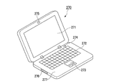
- 1 is an external view showing a notebook personal computer that is an application example of liquid crystal display devices according to first to tenth embodiments.
- FIG. 1 is an external view showing a mobile phone as an application example of a liquid crystal display device according to first to tenth embodiments.
- 1 is an external view showing a thin television that is an application example of a liquid crystal display device according to first to tenth embodiments.
- 1 is an external view showing a notebook personal computer that is an application example of liquid crystal display devices according to first to tenth embodiments.
- FIGS. 1 to 9D An embodiment of the present invention will be described below with reference to FIGS. 1 to 9D.
- this embodiment an example of a liquid crystal display device including a transmissive liquid crystal panel will be described.
- the scale of the size may be changed depending on the component.
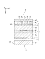
- FIG. 1 is a cross-sectional view of the liquid crystal display device 1 of the present embodiment.
- the liquid crystal display device 1 of the present embodiment includes a liquid crystal panel 2, a backlight 8 (illumination device), and a light control member 9 (light control member).
- the liquid crystal panel 2 includes a first polarizing plate 3, a first retardation film 4 (retardation plate), a liquid crystal cell 5, a second retardation film 6 (retardation plate), a second polarizing plate 7, It has.
- the liquid crystal cell 5 is schematically illustrated, but the detailed structure thereof will be described later.
- the observer sees the display image of the liquid crystal display device 1 through the light control member 9.
- the side on which the light control member 9 is disposed is referred to as the viewing side.
- the side on which the backlight 8 is disposed is referred to as the back side.
- the x axis is defined as the horizontal direction of the screen of the liquid crystal display device.
- the y axis is defined as the vertical direction of the screen of the liquid crystal display device.
- the z axis is defined as the thickness direction of the liquid crystal display device.
- the light emitted from the backlight 8 is modulated by the liquid crystal panel 2, and a predetermined image, character, or the like is displayed by the modulated light.
- the light distribution of the emitted light becomes wider than before entering the light control member 9, and the light is emitted from the light control member 9. The Thereby, the observer can visually recognize the display with a wide viewing angle.
- liquid crystal panel 2 an active matrix transmissive liquid crystal panel will be described as an example.
- the liquid crystal panel applicable to this embodiment is not limited to an active matrix transmissive liquid crystal panel.
- the liquid crystal panel applicable to the present embodiment may be, for example, a transflective type (transmission / reflection type) liquid crystal panel.
- a simple matrix type liquid crystal panel in which each pixel does not include a switching thin film transistor hereinafter abbreviated as TFT may be used.
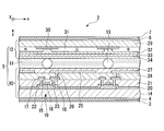
- FIG. 2 is a longitudinal sectional view of the liquid crystal panel 2.
- the liquid crystal cell 5 includes a TFT substrate 10, a color filter substrate 12, and a liquid crystal layer 11.
- the TFT substrate 10 functions as a switching element substrate.
- the color filter substrate 12 is disposed to face the TFT substrate 10.
- the liquid crystal layer 11 is sandwiched between the TFT substrate 10 and the color filter substrate 12.
- the liquid crystal layer 11 is sealed in a space surrounded by the TFT substrate 10, the color filter substrate 12, and a frame-shaped seal member (not shown).
- the sealing member bonds the TFT substrate 10 and the color filter substrate 12 at a predetermined interval.
- the liquid crystal panel 2 of the present embodiment performs display in, for example, a VA (Vertical Alignment, vertical alignment) mode.
- a liquid crystal having a negative dielectric anisotropy is used for the liquid crystal layer 11.
- a spacer 13 is disposed between the TFT substrate 10 and the color filter substrate 12. The spacer 13 is spherical or columnar. The spacer 13 keeps the distance between the TFT substrate 10 and the color filter substrate 12 constant.
- a plurality of pixels are arranged in a matrix on the TFT substrate 10.
- a pixel is a basic unit of display.
- a plurality of source bus lines are formed on the TFT substrate 10 so as to extend in parallel to each other.
- a plurality of gate bus lines are formed on the TFT substrate 10 so as to extend in parallel to each other.
- the plurality of gate bus lines are orthogonal to the plurality of source bus lines.
- On the TFT substrate 10 a plurality of source bus lines and a plurality of gate bus lines are formed in a lattice pattern.
- a rectangular area defined by adjacent source bus lines and adjacent gate bus lines is one pixel.
- the source bus line is connected to the source electrode 17 of the TFT 19.
- the gate bus line is connected to the gate electrode 16 of the TFT 19.
- a TFT 19 having a semiconductor layer 15, a gate electrode 16, a source electrode 17, a drain electrode 18 and the like is formed on the surface of the transparent substrate 14 constituting the TFT substrate 10 on the liquid crystal layer 11 side.
- the transparent substrate 14 for example, a glass substrate can be used.
- a semiconductor layer 15 is formed on the transparent substrate 14.
- Examples of the material of the semiconductor layer 15 include semiconductors such as CGS (Continuous Grain Silicon: continuous grain boundary silicon), LPS (Low-temperature Poly-Silicon: low-temperature polycrystalline silicon), ⁇ -Si (Amorphous Silicon: amorphous silicon), and the like. Material is used.
- a gate insulating film 20 is formed on the transparent substrate 14 so as to cover the semiconductor layer 15.
- a material of the gate insulating film 20 for example, a silicon oxide film, a silicon nitride film, or a laminated film thereof is used.
- a gate electrode 16 is formed on the gate insulating film 20 so as to face the semiconductor layer 15.
- a laminated film of W (tungsten) / TaN (tantalum nitride), Mo (molybdenum), Ti (titanium), Al (aluminum), or the like is used.
- a first interlayer insulating film 21 is formed on the gate insulating film 20 so as to cover the gate electrode 16.
- a material of the first interlayer insulating film 21 for example, a silicon oxide film, a silicon nitride film, or a laminated film thereof is used.
- a source electrode 17 and a drain electrode 18 are formed on the first interlayer insulating film 21.
- a contact hole 22 and a contact hole 23 are formed in the first interlayer insulating film 21 and the gate insulating film 20 so as to penetrate the first interlayer insulating film 21 and the gate insulating film 20.
- the source electrode 17 is connected to the source region of the semiconductor layer 15 through the contact hole 22.
- the drain electrode 18 is connected to the drain region of the semiconductor layer 15 through the contact hole 23.
- a second interlayer insulating film 24 is formed on the first interlayer insulating film 21 so as to cover the source electrode 17 and the drain electrode 18.
- the same material as the first interlayer insulating film 21 described above or an organic insulating material is used.
- a pixel electrode 25 is formed on the second interlayer insulating film 24.
- a contact hole 26 is formed through the second interlayer insulating film 24 in the second interlayer insulating film 24.
- the pixel electrode 25 is connected to the drain electrode 18 through the contact hole 26.
- the pixel electrode 25 is connected to the drain region of the semiconductor layer 15 using the drain electrode 18 as a relay electrode.
- a transparent conductive material such as ITO (Indium Tin Oxide) or IZO (Indium Zinc Oxide) is used.
- the image signal supplied to the source electrode 17 through the source bus line passes through the semiconductor layer 15 and the drain electrode 18 to form a pixel electrode. 25.
- the top gate type TFT shown in FIG. 2 or a bottom gate type TFT may be used as a form of the TFT 19.
- a first vertical alignment film 27 is formed on the entire surface of the second interlayer insulating film 24 so as to cover the pixel electrode 25.
- the first vertical alignment film 27 has an alignment regulating force for vertically aligning liquid crystal molecules constituting the liquid crystal layer 11.
- the first vertical alignment film 27 is a so-called vertical alignment film.
- the first vertical alignment film 27 is subjected to an alignment process using an optical alignment technique. That is, in this embodiment, a photo-alignment film is used as the first vertical alignment film 27.
- a black matrix 30, a color filter 31, a planarization layer 32, a counter electrode 33, and a second vertical alignment film 34 are sequentially formed on the surface of the transparent substrate 29 constituting the color filter substrate 12 on the liquid crystal layer 11 side. ing.
- the black matrix 30 has a function of blocking light transmission in the inter-pixel region.
- the black matrix 30 is formed of, for example, a metal such as Cr (chromium) or a Cr / Cr oxide multilayer film, or a photoresist in which carbon particles are dispersed in a photosensitive resin.
- the color filter 31 contains pigments of red (R), green (G), and blue (B) colors.
- One color filter 31 of R, G, or B is disposed to face one pixel electrode 25 on the TFT substrate 10. Note that the color filter 31 may have a multicolor configuration of three or more colors of R, G, and B.
- the planarization layer 32 is composed of an insulating film that covers the black matrix 30 and the color filter 31.
- the planarizing layer 32 has a function of smoothing and leveling a step formed by the black matrix 30 and the color filter 31.
- a counter electrode 33 is formed on the planarization layer 32.
- a transparent conductive material similar to that of the pixel electrode 25 is used.
- a second vertical alignment film 34 is formed on the entire surface of the counter electrode 33.
- the second vertical alignment film 34 has an alignment regulating force for vertically aligning the liquid crystal molecules constituting the liquid crystal layer 11.
- the second vertical alignment film 34 is a so-called vertical alignment film.
- the alignment process is performed on the second vertical alignment film 34 using a photo-alignment technique. That is, in this embodiment, a photo-alignment film is used as the second vertical alignment film 34.
- the backlight 8 which is an illumination device includes a light source 36 and a light guide 37.
- the light source 36 is disposed on the end face of the light guide 37.
- As the light source 36 for example, a light emitting diode, a cold cathode tube, or the like is used.
- the backlight 8 of the present embodiment is an edge light type backlight.
- the light guide 37 has a function of guiding the light emitted from the light source 36 to the liquid crystal panel 2.
- a resin material such as acrylic resin is used.
- the light incident on the end surface of the light guide 37 from the light source 36 propagates by being totally reflected inside the light guide 37 and is emitted from the upper surface (light emission surface) of the light guide 37 with a substantially uniform intensity.
- a scattering sheet and a prism sheet are disposed on the upper surface of the light guide 37, and a scattering sheet is disposed on the lower surface of the light guide 37.
- the light emitted from the upper surface of the light guide 37 is scattered by the scattering sheet, then condensed by the prism sheet, and is emitted after being substantially parallelized.
- White PET may be used as the scattering sheet.
- the prism sheet for example, BEF (trade name) manufactured by Sumitomo 3M may be used.
- the backlight 8 does not need to have directivity.
- a backlight hereinafter, sometimes referred to as a normal backlight
- the backlight 8 may have directivity.
- a first polarizing plate 3 is provided between the backlight 8 and the liquid crystal cell 5.
- the first polarizing plate 3 functions as a polarizer.
- a second polarizing plate 7 is provided between the liquid crystal cell 5 and the light control member 9.
- the second polarizing plate 7 functions as a polarizer.
- the transmission axis of the first polarizing plate 3 and the transmission axis of the second polarizing plate 7 are in a crossed Nicols arrangement.
- the 1st phase difference film 4 for compensating the phase difference of light is provided between the 1st polarizing plate 3 and the liquid crystal cell 5.
- a second retardation film 6 is provided between the second polarizing plate 7 and the liquid crystal cell 5 to compensate for the phase difference of light.
- retardation film As the retardation film (first retardation film 4, second retardation film 6) of this embodiment, a WV film manufactured by Fuji Film Co., Ltd. is used.
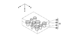
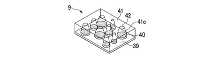
- FIG. 3 is a perspective view of the light control member 9 as seen from the viewing side.
- FIG. 4 is a schematic diagram of the light control member 9.
- the upper left side is a plan view of the light control member 9.
- the lower left side is a cross-sectional view along the line AA in the plan view of the upper left side.
- the upper right stage is a cross-sectional view along the line BB in the plan view of the upper left stage.
- the light control member 9 includes a base material 39, a plurality of light shielding layers 40, and a light diffusion portion 41, as shown in FIG.
- the plurality of light shielding layers 40 are formed on one surface of the base material 39 (a surface opposite to the viewing side).
- the light diffusion portion 41 is formed in an area other than the formation area of the light shielding layer 40 on one surface of the base material 39.
- the light control member 9 is disposed on the second polarizing plate 7 with the light diffusion portion 41 facing the second polarizing plate 7 and the base material 39 facing the viewing side.
- the light control member 9 is fixed to the second polarizing plate 7 through the adhesive layer 43.
- the base material 39 examples include transparent resin base materials such as triacetyl cellulose (TAC) film, polyethylene terephthalate (PET), polycarbonate (PC), polyethylene naphthalate (PEN), and polyethersulfone (PES) film.
- TAC triacetyl cellulose
- PET polyethylene terephthalate
- PC polycarbonate
- PEN polyethylene naphthalate
- PES polyethersulfone
- the base material 39 becomes a base when the material for the light shielding layer 40 and the light diffusion portion 41 is applied later in the manufacturing process.
- the base material 39 needs to have heat resistance and mechanical strength in a heat treatment step during the manufacturing process. Therefore, as the base material 39, a glass base material or the like may be used in addition to the resin base material. However, it is preferable that the thickness of the base material 39 is as thin as possible without impairing heat resistance and mechanical strength.
- the total light transmittance of the base material 39 is preferably 90% or more as defined in JIS K7361-1. When the total light transmittance is 90% or more, sufficient transparency can be obtained.
- a transparent resin substrate having a thickness of 100 ⁇ m is used as an example.
- the light shielding layer 40 is randomly arranged as viewed from the normal direction of the main surface of the base material 39.
- the light shielding layer 40 is made of an organic material having light absorption and photosensitivity such as black resist and black ink.
- a metal film such as Cr (chromium) or a Cr / Cr oxide multilayer film may be used.
- the light diffusing section 41 is made of an organic material having optical transparency and photosensitivity such as acrylic resin and epoxy resin. Further, the total light transmittance of the light diffusing portion 41 is preferably 90% or more in accordance with JIS K7361-1. When the total light transmittance is 90% or more, sufficient transparency can be obtained.
- the light diffusing portion 41 has a light exit end face 41a, a light incident end face 41b, and a reflecting face 41c.
- the light emission end surface 41 a is a surface in contact with the base material 39.
- the light incident end surface 41b is a surface facing the light emitting end surface 41a.
- the reflection surface 41 c is a tapered side surface of the light diffusion portion 41.
- the reflection surface 41c is a surface that reflects light incident from the light incident end surface 41b.
- the area of the light incident end face 41b is larger than the area of the light exit end face 41a.
- the light diffusion part 41 is a part that contributes to the transmission of light in the light control member 9.
- the light L1 is emitted from the light emission end face 41a without being reflected by the reflection surface 41c.
- the light L2 is totally reflected by the reflecting surface 41c of the light diffusing unit 41 and guided in a state of being substantially confined inside the light diffusing unit 41, and the light emitting end surface 41a. Is injected from.
- the light control member 9 is arranged so that the base material 39 faces the viewing side. Therefore, of the two opposing surfaces of the light diffusing portion 41, the surface with the smaller area becomes the light emission end surface 41a. On the other hand, the surface with the larger area becomes the light incident end surface 41b.
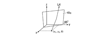
- the inclination angle of the reflection surface 41c of the light diffusion portion 41 (the angle formed between the light incident end surface 41b and the reflection surface 41c) may be 80 ° ⁇ 5 °, and is about 80 ° as an example.
- the inclination angle of the reflection surface 41c of the light diffusion portion 41 is not particularly limited as long as it is an angle that can sufficiently diffuse incident light when emitted from the light control member 9.
- the inclination angle of the reflection surface 41c of the light diffusing unit 41 is constant.
- the height from the light incident end surface 41 b to the light emitting end surface 41 a of the light diffusion portion 41 is set to be larger than the layer thickness of the light shielding layer 40.
- the layer thickness of the light shielding layer 40 is about 150 nm as an example.
- the height from the light incident end surface 41b of the light diffusion portion 41 to the light emitting end surface 41a is about 20 ⁇ m.
- a portion surrounded by the reflection surface 41 c of the light diffusion portion 41 and the light shielding layer 40 is a hollow portion 42. Air exists in the hollow portion 42.
- the refractive index of the base material 39 and the refractive index of the light diffusion part 41 are substantially equal.
- the reason is as follows. For example, consider a case where the refractive index of the base material 39 and the refractive index of the light diffusion portion 41 are greatly different. In this case, when light incident from the light incident end surface 41 b exits from the light diffusion portion 41, unnecessary light refraction or reflection may occur at the interface between the light diffusion portion 41 and the base material 39. In this case, there is a possibility that problems such as failure to obtain a desired viewing angle and a decrease in the amount of emitted light may occur.
- the light diffusion portion 41 is formed of, for example, a transparent acrylic resin
- the reflection surface 41c of the light diffusion portion 41 becomes an interface between the transparent acrylic resin and air.
- the hollow portion 42 may be filled with another low refractive index material.
- the difference in the refractive index at the interface between the inside and the outside of the light diffusing portion 41 is maximized when air is present rather than when any low refractive index material is present outside. Therefore, according to Snell's law, in the configuration of the present embodiment, the critical angle is the smallest, and the incident angle range in which the light is totally reflected by the reflection surface 41c of the light diffusion portion 41 is the widest. As a result, light loss is further suppressed, and high luminance can be obtained.
- the planar shape of the light shielding layer 40 as viewed from the normal direction of the substrate 39 is circular.
- the diameter of the light shielding layer 40 is, for example, about 15 ⁇ m.
- the ratio of the occupied area of the light shielding layer 40 to the total area of the base material 39 is, for example, 30% ⁇ 10%.
- a portion corresponding to the lower part of the light shielding layer 40 is a truncated cone-shaped hollow part 42.
- the light control member 9 has a plurality of hollow portions 42.
- a light diffusing portion 41 is continuously provided in a portion other than the plurality of hollow portions 42.
- the planar shape of the light shielding layer 40 may include an ellipse, a polygon, a semicircle, and the like.
- the planar shape of the light shielding layer 40 is preferably a shape having line symmetry of two or more axes.
- the shape having line symmetry of two or more axes refers to a shape that is line symmetric with respect to at least two or more line segments. For example, a rectangle is mentioned as a shape symmetrical with respect to two line segments.
- the axis of line symmetry is considered to be infinite, so it is included in a shape having line symmetry of two or more axes.
- the planar shape of the light shielding layer 40 has a shape having line symmetry of two or more axes
- the light scattering characteristics of the light control member 9 are two or more axes when viewed from the normal direction of the liquid crystal panel 2. It has symmetry. Further, a part of the light shielding layer 40 may be formed to overlap.
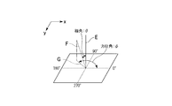
- FIG. 5 is a diagram for explaining the definition of the polar angle and the azimuth angle.
- an angle formed by the viewing direction F of the observer with respect to the normal direction E of the screen of the liquid crystal display device 1 is defined as a polar angle ⁇ .
- the angle formed by the direction of the line segment G when the line-of-sight direction F of the observer is projected on the screen with reference to the positive direction (0 ° direction) of the x-axis is defined as an azimuth angle ⁇ .
- FIG. 6 is a front view of the liquid crystal display device 1.
- the horizontal direction (x-axis direction) is the azimuth angle ⁇ : 0 ° -180 ° direction.
- the vertical direction (y-axis direction) is the azimuth angle ⁇ : 90 ° -270 ° direction.
- the transmission axis of the first polarizing plate 3 is the azimuth angle ⁇ : 90 ° -270 ° direction
- the transmission axis of the second polarizing plate 7 is the azimuth angle ⁇ : 0 ° -180 ° direction. It is.
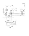
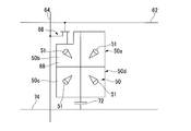
- FIG. 7 schematically shows the electrical configuration of one pixel of the liquid crystal display device 1 of the present embodiment.
- the pixel 50 is connected to the TFT 66 and the auxiliary capacitor (CS) 72.
- the gate electrode of the TFT 66 is connected to the scanning line 62.
- the source electrode is connected to the signal line 64.
- the auxiliary capacitor 72 is connected to an auxiliary capacitor line (CS bus line) 74.
- the auxiliary capacitance 72 includes an auxiliary capacitance electrode electrically connected to the pixel electrode 68, an auxiliary capacitance counter electrode electrically connected to the auxiliary capacitance wiring 74, and an insulating layer (not shown) provided therebetween. Is formed by.
- the liquid crystal molecules 51 viewed from the normal direction of the liquid crystal panel 2 are shown in a conical shape.
- the apex of the cone means the end of the liquid crystal molecule 51 on the back side (TFT substrate side).
- the bottom surface of the cone indicates the end of the liquid crystal molecule on the viewing side (color filter substrate side).
- the director of the liquid crystal molecules 51 is defined as a direction from an end on the back side of the liquid crystal molecules toward an end on the viewing side.
- the pixel 50 employs a four-domain VA having four domains 50a, 50b, 50c, and 50d.
- the liquid crystal molecules 51 included in the four domains 50a, 50b, 50c, and 50d will be described in more detail below.
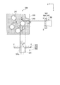
- FIG. 8 is a schematic diagram showing an arrangement relationship between the light control member 9 and the pixel 50 including the VA mode liquid crystal included in the liquid crystal display device 1.
- the light control member 9 is disposed on the pixel 50.
- the pixel 50 and the light control member 9 are shown in parallel in FIG.
- the liquid crystal molecules 51 included in the pixel 50 are aligned substantially vertically when no voltage is applied.
- the directors of the liquid crystal molecules 51 included in the first domain 50a are oriented in the direction of the azimuth angle ⁇ : 45 °, and are inclined so that the polar angle ⁇ is larger than 0 °.
- the liquid crystal molecules 51 By aligning the liquid crystal molecules 51 in this way, in the first domain 50a, the liquid crystal molecules 51 have an azimuth angle ⁇ of 45 ° and a polar angle of 90 ° at the center in the thickness direction of the liquid crystal layer 11 when a voltage is applied. Tilt down closer to °.
- the director of the liquid crystal molecules 51 included in the second domain 50b is oriented in the direction of the azimuth angle ⁇ : 135 °, and is inclined so that the polar angle ⁇ is larger than 0 °.
- the liquid crystal molecules 51 By aligning the liquid crystal molecules 51 in this manner, in the second domain 50b, the liquid crystal molecules 51 have an azimuth angle ⁇ : 135 ° and a polar angle of 90 ° at the center in the thickness direction of the liquid crystal layer 11 when a voltage is applied. Tilt down closer to °.
- the director of the liquid crystal molecules 51 included in the third domain 50c is oriented in the direction of the azimuth angle ⁇ : 225 °, and is inclined so that the polar angle ⁇ is larger than 0 °.
- the liquid crystal molecules 51 have an azimuth angle ⁇ : 225 ° and a polar angle of 90 at the center in the thickness direction of the liquid crystal layer 11 when a voltage is applied. Tilt down closer to °.
- the director of the liquid crystal molecules 51 included in the fourth domain 50d is oriented in the direction of the azimuth angle ⁇ : 315 °, and is inclined so that the polar angle ⁇ is larger than 0 °.
- the liquid crystal molecules 51 By aligning the liquid crystal molecules 51 in this manner, in the fourth domain 50d, the liquid crystal molecules 51 have an azimuth angle ⁇ : 315 ° and a polar angle of 90 at the center in the thickness direction of the liquid crystal layer 11 when a voltage is applied. Tilt down closer to °.
- the liquid crystal molecules 51 included in the first to fourth domains 50a to 50d are oriented in a direction in which the azimuth is 90 ° different from each other. Therefore, the liquid crystal molecules 51 included in the first to fourth domains 50a to 50d are tilted in directions different from each other in azimuth by 90 ° when a voltage is applied. That is, with respect to the axis in the direction of the azimuth angle ⁇ : 0 ° -180 °, the liquid crystal molecules 51 included in the first domain 50a are tilted so as to be line symmetric with the liquid crystal molecules 51 included in the fourth domain 50d.
- the liquid crystal molecules 51 included in the domain 50b are tilted so as to be line symmetric with the liquid crystal molecules 51 included in the third domain 50c. Further, the liquid crystal molecules 51 included in the first domain 50a are tilted so as to be line-symmetric with the liquid crystal molecules 51 included in the first domain 50b with respect to the axis in the direction of the azimuth angle ⁇ : 90 ° to 270 °.
- the liquid crystal molecules 51 included in the domain 50c are tilted so as to be line-symmetric with the liquid crystal molecules 51 included in the fourth domain 50d. That is, the liquid crystal display device 1 is tilted so as to have biaxial line symmetry as viewed from the normal direction.
- the liquid crystal molecules 51 in the vicinity of the first light distribution film 27 and the second light distribution film 34 are restricted in light distribution by the first light distribution film 27 and the second light distribution film 34, so that even when a voltage is applied. It remains almost vertical.
- the light control member 9 is disposed on the light emission side of the liquid crystal panel 2.
- the light control member 9 is mixed by the light control member 9.
- the variation in the luminance change depending on the polar angle ⁇ is averaged, and as a result, the change in the gamma characteristic depending on the polar angle ⁇ is alleviated.
- the viewing angle characteristic is improved by combining the light control member 9 of the present embodiment with the liquid crystal display device 1 adopting the 4-domain VA method.
- FIGS. 9A to 9D are perspective views showing the manufacturing process of the light control member 9 step by step.
- the manufacturing method of the light control member 9 constituting the liquid crystal display device 1 having the above configuration will be mainly described.
- the outline of the manufacturing process of the liquid crystal panel 2 will be described first.
- the TFT substrate 10 and the color filter substrate 12 are respectively produced.
- the surface of the TFT substrate 10 on which the TFT 19 is formed and the surface of the color filter substrate 12 on which the color filter 31 is formed are arranged to face each other.
- the TFT substrate 10 and the color filter substrate 12 are bonded together via a seal member.
- liquid crystal is injected into a space surrounded by the TFT substrate 10, the color filter substrate 12, and the seal member.
- the first retardation film 4, the first polarizing plate 3, the second retardation film 6, and the second polarizing plate 7 are bonded to both surfaces of the liquid crystal cell 5 thus formed using an optical adhesive or the like.
- the liquid crystal panel 2 is completed through the above steps.
- the manufacturing method of the TFT substrate 10 and the color filter substrate 12 may be a conventional method, and the description thereof is omitted.
- a triacetyl cellulose base material 39 having a thickness of 100 ⁇ m is prepared.
- a black negative resist containing carbon as a light shielding part material is applied to one surface of the base material 39 by using a spin coating method.
- the coating film 45 with a film thickness of 150 nm is formed.
- the base material 39 on which the coating film 45 is formed is placed on a hot plate, and the coating film 45 is pre-baked at a temperature of 90 ° C. Thereby, the solvent in the black negative resist is volatilized.
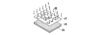
- an exposure apparatus Exposure is performed by irradiating the coating film 45 with light L through a photomask 47 in which a plurality of opening patterns 46 having a circular planar shape, for example, are formed.
- an exposure apparatus using a mixed line of i-line having a wavelength of 365 nm, h-line having a wavelength of 404 nm, and g-line having a wavelength of 436 nm is used.
- the exposure dose is 100 mJ / cm 2 .
- the coating film 45 made of black negative resist is developed using a dedicated developer, dried at 100 ° C., and the planar shape is as shown in FIG. 9B.
- a plurality of circular light shielding layers 40 are formed on one surface of the base material 39.
- the transparent negative resist is exposed using the light shielding layer 40 made of a black negative resist as a mask to form the hollow portion 42. Therefore, the position of the opening pattern 46 of the photomask 47 corresponds to the position where the hollow portion 42 is formed.
- the circular light shielding layer 40 corresponds to a non-formation region (hollow portion 42) of the light diffusion portion 41 in the next step.
- the plurality of opening patterns 46 are all circular patterns.
- the diameter of the opening pattern 46 is composed of various sizes.
- the arrangement of the intervals (pitch) between the adjacent opening patterns 46 is neither regular nor periodic.
- the interval (pitch) between the opening patterns 46 is preferably smaller than the interval (pitch, for example, 150 ⁇ m) between the pixels of the liquid crystal panel 2.
- the light shielding layer 40 is formed by a photolithography method using a black negative resist, but the present invention is not limited to this. In addition to this, if a photomask in which the opening pattern 46 and the light shielding pattern of the present embodiment are reversed is used, a positive resist having light absorption can also be used. Alternatively, the light shielding layer 40 may be directly formed using a vapor deposition method, a printing method, or the like.
- a transparent negative resist made of an acrylic resin is applied to the upper surface of the light shielding layer 40 as a light diffusion portion material by using a spin coating method.
- the coating film 48 with a film thickness of 20 ⁇ m is formed.
- the base material 39 on which the coating film 48 is formed is placed on a hot plate, and the coating film 48 is pre-baked at a temperature of 95 ° C. Thereby, the solvent in the transparent negative resist is volatilized.
- the coating film 48 is irradiated with light F from the substrate 39 side using the light shielding layer 40 as a mask to perform exposure.
- an exposure apparatus using a mixed line of i-line having a wavelength of 365 nm, h-line having a wavelength of 404 nm, and g-line having a wavelength of 436 nm is used.
- the exposure amount is 500 mJ / cm 2 .
- the substrate 39 on which the coating film 48 is formed is placed on a hot plate, and post-exposure baking (PEB) of the coating film 48 is performed at a temperature of 95 ° C.
- PEB post-exposure baking
- the coating film 48 made of a transparent negative resist is developed using a dedicated developer, post-baked at 100 ° C., and a transparent resin layer 41 having a plurality of hollow portions 42 is used as a base material as shown in FIG. 9D. 39 on one side.
- the transparent negative resist constituting the coating film 48 is radially spread so as to spread outward from the non-formation region of the light shielding layer 40. Exposed. Thereby, the forward tapered hollow portion 42 is formed.
- the light diffusion portion 41 has a reverse tapered shape. The inclination angle of the reflection surface 41c of the light diffusion portion 41 can be controlled by the degree of diffusion of the diffused light.
- the light F used here parallel light, diffused light, or light whose intensity at a specific emission angle is different from that at another emission angle, that is, light having strength at a specific emission angle can be used.
- the inclination angle of the reflection surface 41c of the light diffusing unit 41 becomes a single inclination angle of, for example, about 60 ° to 90 °.
- the tilt angle changes continuously, and the cross-sectional shape becomes a curved inclined surface.
- an inclined surface having a slope angle corresponding to the strength is obtained.
- the inclination angle of the reflection surface 41c of the light diffusing unit 41 can be adjusted.
- a diffusion plate having a haze of about 50 is arranged on the optical path of the light emitted from the exposure apparatus, and the diffusion plate Irradiate light through.
- the total light transmittance of the light control member 9 is preferably 90% or more. When the total light transmittance is 90% or more, sufficient transparency is obtained, and the optical performance required for the light control member 9 can be sufficiently exhibited.
- the total light transmittance is as defined in JIS K7361-1. In this embodiment, an example in which a liquid resist is used has been described, but a film resist may be used instead of this configuration.
- the completed light control member 9 is placed with the base material 39 facing the viewing side and the light diffusion portion 41 facing the second polarizing plate 7 with the adhesive layer 43 interposed therebetween. Affix to the liquid crystal panel 2.
- the light control member 9 is disposed on the light emission side of the liquid crystal panel 2, the light incident on the light control member 9 is before entering the light control member 9. Is emitted from the light control member 9 in a state where the angular distribution is widened. Therefore, even if the observer inclines the line of sight from the front direction (normal direction) of the liquid crystal display device 1, a good display can be visually recognized.
- an interference fringe pattern is visually recognized when the period of each pattern is slightly shifted.
- a light control member in which a plurality of light diffusion portions are arranged in a matrix and a liquid crystal panel in which a plurality of pixels are arranged in a matrix are overlapped, the periodic pattern by the light diffusion portions of the light control members and the liquid crystal panel.
- a plurality of light shielding layers 40 are randomly arranged in a plane.
- the light diffusion portion 41 is formed in a region other than the region where the light shielding layer 40 is formed. Therefore, moire due to interference does not occur with the regular arrangement of the pixels of the liquid crystal panel 2, and the display quality can be maintained.
- the arrangement of the plurality of light shielding layers 40 is random, but the arrangement of the plurality of light shielding layers 40 is not necessarily random. If the arrangement of the plurality of light shielding layers 40 is aperiodic, the occurrence of moire can be suppressed. Further, when some moiré is allowed depending on the situation and application, a plurality of light shielding layers 40 may be periodically arranged.
- FIG. 10 is a top view of the light control member 309.
- the light control member 309 of the present embodiment is provided with a plurality of light diffusion portions 341 that are scattered on one surface of a base material.
- the planar shape of the light diffusing portion 341 viewed from the normal direction of the substrate is circular.
- a portion corresponding to the lower side of the light shielding layer 340 becomes a hollow portion 342. Air exists in the hollow portion 342.
- the light control member 309 has a continuous hollow portion 342 in which air exists. Light diffusing portions 341 are scattered in portions other than the hollow portion 342.
- the light control member 309 is disposed on the light emission side of the liquid crystal panel 2. Even when such a light control member 309 is used, it is possible to suppress a change in gamma characteristics when the display screen is viewed obliquely, and to realize a display image with excellent viewing angle characteristics.
- planar shape of the light diffusion portion 341 may include a circular shape, a polygonal shape, a semicircular shape, or the like. Further, the openings of the light diffusion portion 341 may be formed to overlap each other.
- FIGS. 11A to 11E a second embodiment of the present invention will be described with reference to FIGS. 11A to 11E.
- the basic configuration of the liquid crystal display device of this embodiment is the same as that of the first embodiment, and the shape of the light shielding layer in the light control member is different from that of the first embodiment. Therefore, in this embodiment, the description of the basic configuration of the liquid crystal display device is omitted, and the light shielding layer is described.
- FIGS. 11A to 11E are plan views of the light shielding layer of the present embodiment.
- the shape of the light shielding layer of the present embodiment is a shape having line symmetry of two or more axes.
- FIG. 11A an example of the light shielding layer 40 having a circular planar shape is shown.
- a light diffusing portion 40G having a square planar shape is used.
- a light diffusing portion 40H whose planar shape is a regular octagon may be used.
- a light diffusing portion 40I having a shape in which two opposite sides of a square are curved outward may be used.
- a light diffusing unit 40J having a shape in which two rectangles intersect in two orthogonal directions may be used.
- the shapes of FIGS. 11B to 11E may be rotated in a plurality of directions. For example, in the case of the square light diffusing unit 40G shown in FIG. 11B, light diffuses in a direction perpendicular to each side of the square.
- FIGS. 12A, 12B, 13A, and 13B The basic configuration of the liquid crystal display device of the present embodiment is the same as that of the first embodiment, and the configuration of the reflection surface of the light diffusion portion in the light control member is different from that of the first embodiment. Therefore, in this embodiment, description of the basic structure of a liquid crystal display device is abbreviate
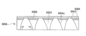
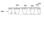
- FIGS. 12A and 12B are cross-sectional views of the light control members 609A and 609B of the present embodiment. As shown in FIGS. 12A and 12B, the light control members 609A and 609B of the present embodiment are different from the light control member 9 of the first embodiment in the configuration of the reflection surfaces of the light diffusion portions 641A and 641B.
- the inclination angle of the reflection surface 41c of the light diffusing unit 40 is constant.
- the inclination angles of the reflection surfaces of the light diffusion portions 641A and 641B continuously change.
- the cross-sectional shape of the reflection surface of the light diffusion portions 641A and 641B is a curved inclined surface.
- the reflection surface 641Ac of the light diffusion portion 641A is curved toward the hollow portion 642A, and the reflection surface 641Ac side of the hollow portion 642A is concave.
- the reflection surface 641Bc of the light diffusion portion 641B is curved toward the hollow portion 642B, and the portion of the hollow portion 642B on the reflection surface 641Bc side is convex.
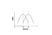
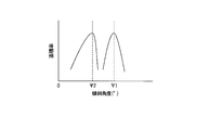
- FIG. 13A and 13B are diagrams for explaining the relationship between the inclination angle of the reflection surface of the light diffusion portion and the area ratio.
- FIG. 13A is a diagram in the case where the distribution of the inclination angle of the reflection surface of the light diffusion portion is the same between the first reflection surface and the second reflection surface.
- FIG. 13B is a diagram in the case where the distribution of the inclination angle of the reflection surface of the light diffusion portion is different between the first reflection surface and the second reflection surface.
- the horizontal axis represents the inclination angle of the reflection surface of the light diffusion portion.
- the vertical axis represents the area ratio of the reflection surface of the light diffusion portion.
- the area ratio is the ratio of the area of a portion having a certain inclination angle to the area of the entire reflection surface when the reflection surface of the light diffusion portion is viewed from the side.
- the inclination angle is an angle formed by a tangent line at a predetermined position of the curved portion of the reflection surface and the light incident end surface of the light diffusion portion.
- the tilt angle ⁇ 1 of the first reflecting surface is larger than the tilt angle ⁇ 2 of the second reflecting surface will be described.
- the inclination angle of the reflection surface of the light diffusing portion has a width in the angle distribution around the main inclination angle.
- the distribution of the inclination angle of the reflection surface of the light diffusing section may be the same distribution for the inclination angle ⁇ 1 of the first reflection surface and the inclination angle ⁇ 2 of the second reflection surface.
- different inclination distributions may be used for the inclination angle ⁇ 1 of the first reflection surface and the inclination angle ⁇ 2 of the second reflection surface.
- the inclination angle ⁇ 1 of the first reflecting surface contributes more to the symmetry of the luminance distribution than the inclination angle ⁇ 2 of the second reflecting surface. Therefore, in order to improve the symmetry of the luminance distribution, the distribution of the inclination angle ⁇ 1 of the first reflecting surface is preferably narrow.
- the light control member 609A or 609B is disposed on the light emission side of the liquid crystal panel 2. Even when such a light control member 609A or 609B is used, it is possible to suppress a change in gamma characteristics when the display screen is viewed from an oblique direction, and to realize a display image with excellent viewing angle characteristics.
- FIGS. 14A and 14B a fifth embodiment of the present invention will be described with reference to FIGS. 14A and 14B.
- the basic configuration of the liquid crystal display device of the present embodiment is the same as that of the fourth embodiment, and the configuration of the reflection surface of the light diffusion portion in the light control member is different from that of the fourth embodiment. Therefore, in this embodiment, description of the basic structure of a liquid crystal display device is abbreviate
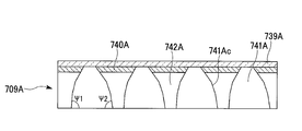
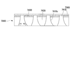
- FIGS. 14A and 14B are cross-sectional views of the light control members 709A and 709B of the present embodiment. As shown in FIGS. 14A and 14B, the light control members 709A and 709B of the present embodiment are different from the light control members 609A and 609B of the fourth embodiment in the configuration of the reflection surface of the light diffusion portion.
- the inclination angles of the reflection surfaces of the light diffusion portions 641A and 641B continuously change, and the cross sections of the reflection surfaces of the light diffusion portions 641A and 641B
- the shape was a curved inclined surface.
- the reflection surfaces of the light diffusion portions 741A and 741B have a plurality of different inclination angles.
- the cross-sectional shape of the reflection surface of the light diffusion portions 741A and 741B is a polygonal inclined surface.
- the reflection surface 741Ac of the light diffusion portion 741A has three inclined surfaces with different inclination angles, and the portion of the hollow portion 742A on the reflection surface 741Ac side is concave.
- the reflection surface 741Bc of the light diffusion portion 741B has three inclined surfaces having different inclination angles, and the portion of the hollow portion 742B on the reflection surface 741Bc side is convex.
- the light control members 709A and 709B of the present embodiment are used, it is possible to suppress a change in gamma characteristics when the display screen is viewed obliquely, and to realize a display image with excellent viewing angle characteristics.
- FIGS. The basic configuration of the liquid crystal display device of this embodiment is the same as that of the first embodiment, and the configuration of the pixels of the liquid crystal panel 2 is different from that of the first embodiment.
- the liquid crystal panel 2 of the present embodiment has a pixel configuration that employs so-called multi-pixel driving. Therefore, in this embodiment, the description of the basic configuration of the liquid crystal display device is omitted, and the pixels of the liquid crystal panel 2 will be described.
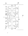
- FIG. 15 schematically shows an electrical configuration of one pixel of the liquid crystal display device 200 of the present embodiment.
- the pixel 60 is divided into sub-pixels 60a and 60b.
- a TFT 66a and an auxiliary capacitor (CS) 72a are connected to the sub-pixel 60a.
- a TFT 66b and an auxiliary capacitor 72b are connected to the sub-pixel 60b.
- the gate electrodes of the TFTs 66 a and 66 b are connected to the scanning line 62.
- the source electrodes are connected to a common (identical) signal line 64.
- the auxiliary capacitors 72a and 72b are connected to an auxiliary capacitor line (CS bus line) 74a and an auxiliary capacitor line 74b, respectively.
- the auxiliary capacitances 72a and 72b are provided between the auxiliary capacitance electrode electrically connected to the sub-pixel electrodes 68a and 68b, the auxiliary capacitance counter electrode electrically connected to the auxiliary capacitance wirings 74a and 74b, respectively.
- the insulating layer (not shown) is formed.
- the storage capacitor counter electrodes of the storage capacitors 72a and 72b are independent from each other, and different storage capacitor counter voltages can be supplied from the storage capacitor lines 74a and 74b, respectively.
- the sub-pixel 60a further has four domains 61a, 61b, 61c, and 61d.
- the liquid crystal molecules 51 included in the domain 61a, the liquid crystal molecules 51 included in the domain 61b, the liquid crystal molecules 51 included in the domain 61c, and the liquid crystal molecules 51 included in the domain 61d have an azimuth angle. Tilt in different directions by 90 °.
- the sub-pixel 60b further includes four domains 61e, 61f, 61g, and 61h.
- the liquid crystal molecules 51 included in the domain 61e, the liquid crystal molecules 51 included in the domain 61f, the liquid crystal molecules 51 included in the domain 61g, and the liquid crystal molecules 51 included in the domain 61h have an azimuth angle. Tilt in different directions by 90 °.
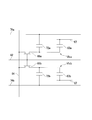
- FIG. 16 schematically shows an equivalent circuit for one pixel of the liquid crystal display device 200.
- the liquid crystal layers of the respective sub-pixels 60a and 60b are represented as liquid crystal layers 63a and 63b.
- the liquid crystal capacitances formed by the subpixel electrodes 68a and 68b, the liquid crystal layers 63a and 63b, and the counter electrode 67 are Clca and Clcb, respectively.
- the capacitance values of the liquid crystal capacitors Clca and Clcb are the same value CLC (V).
- the value of CLC (V) depends on the effective voltage (V) applied to the liquid crystal layers of the subpixels 60a and 60b.
- the auxiliary capacitors 72a and 72b that are independently connected to the liquid crystal capacitors of the sub-pixels 60a and 60b are Ccsa and Ccsb, respectively, and their capacitance values are the same value CCS.
- One electrode of the auxiliary capacitor Ccsa of the subpixel 60a is a subpixel electrode.
- the subpixel electrode 68a of the liquid crystal capacitor Clca and the subpixel electrode of the auxiliary capacitor Ccsa are connected to the drain electrode of the TFT 66a provided for driving the subpixel 60a.
- the other electrode of the liquid crystal capacitor Clca is a counter electrode.
- the other electrode of the auxiliary capacitance Ccsa is connected to the auxiliary capacitance wiring 74a.
- One electrode of the auxiliary capacitor Ccsb of the subpixel 60b is a subpixel electrode.
- the subpixel electrode 68b of the liquid crystal capacitor Clcb and the subpixel electrode of the auxiliary capacitor Ccsb are connected to the drain electrode of the TFT 66b provided for driving the subpixel 60b.
- the other electrode of the liquid crystal capacitor Clcb is a counter electrode.
- the other electrode of the auxiliary capacitance Ccsb is connected to the auxiliary capacitance wiring 74b.
- the gate electrodes of the TFT 66 a and the TFT 66 b are both connected to the scanning line 62. All the source electrodes are connected to the signal line 64.
- 17A to 17F schematically show the timing of each voltage when driving the liquid crystal display device 200 of the present embodiment.
- FIG. 17 shows the voltage waveform Vs of the signal line 64.
- FIG. 17B shows a voltage waveform Vcsa of the auxiliary capacitance line 74a.
- FIG. 17C shows the voltage waveform Vcsb of the auxiliary capacitance line 74b.
- FIG. 17D shows the voltage waveform Vg of the scanning line 62.
- FIG. 17E shows the voltage waveform Vlca of the pixel electrode 68a of the sub-pixel 60a.
- FIG. 17F shows the voltage waveform Vlcb of the pixel electrode 68b of the sub-pixel 60b.
- the broken line in the figure shows the voltage waveform COMMON (Vcom) of the counter electrode 67.
- the voltage of Vg changes from VgL to VgH, so that the TFT 66a and the TFT 66b are simultaneously turned on (on state), and the voltage Vs of the signal line 64 is applied to the subpixel electrodes 68a and 68b of the subpixels 60a and 60b. Then, the subpixels 60a and 60b are charged. Similarly, the auxiliary capacitors Csa and Csb of the respective sub-pixels are charged from the signal line.
- the voltage Vg of the scanning line 62 changes from VgH to VgL, so that the TFT 66a and the TFT 66b are simultaneously turned off (OFF state), and the subpixels 60a and 60b and the auxiliary capacitors Csa and Csb are all signal lines 64. And electrically insulated.
- the voltages Vlca and Vlcb of the respective sub-pixel electrodes decrease by substantially the same voltage Vd and are expressed by the following equations.
- Vlca Vs ⁇ Vd (1)
- Vlcb Vs ⁇ Vd (2)
- Vcsa and Vcsb of the respective auxiliary capacitance lines are represented by the following equations.
- Vcsa Vcom ⁇ Vad (3)
- Vcsb Vcom + Vad (4)
- Vcsa of the auxiliary capacitance line 74a connected to the auxiliary capacitance Csa changes from Vcom ⁇ Vad to Vcom + Vad
- the voltage Vcsb of the auxiliary capacitance line 74b connected to the auxiliary capacitance Csb changes from Vcom + Vad to Vcom ⁇ Vad. It changes by twice Vad.
- the voltages Vlca and Vlcb of the respective subpixel electrodes change as follows.
- Vlca Vs ⁇ Vd + 2 ⁇ K ⁇ Vad
- Vlcb Vs ⁇ Vd ⁇ 2 ⁇ K ⁇ Vad (6)
- K CCS / (CLC (V) + CCS).
- Vcsa changes from Vcom + Vad to Vcom ⁇ Vad
- Vcsb changes from Vcom ⁇ Vad to Vcom + Vad by twice Vad
- Vlca and Vlcb are also changed from Equation (7) and Equation (8) to Equation (9), respectively.
- Vlca Vs ⁇ Vd + 2 ⁇ K ⁇ Vad
- Vlcb Vs ⁇ Vd ⁇ 2 ⁇ K ⁇ Vad
- Vlca Vs ⁇ Vd (9)
- Vlcb Vs ⁇ Vd (10)
- Vcsa changes from Vcom ⁇ Vad to Vcom + Vad
- Vcsb changes from Vcom + Vad to Vcom ⁇ Vad by twice Vad
- Vlca and Vlcb are also changed from Equation (11) and Equation (12) to Equation (13), respectively.
- Vlca Vs ⁇ Vd (11)
- Vlcb Vs ⁇ Vd (12)
- Vlca Vs ⁇ Vd + 2 ⁇ K ⁇ Vad (13)
- Vlcb Vs ⁇ Vd ⁇ 2 ⁇ K ⁇ Vad (14)
- V1 and V2 applied to the liquid crystal layers 13a and 13b of the sub-pixels 60a and 60b are shown below.
- V1 Vlca ⁇ Vcom (17)
- V2 Vlcb ⁇ Vcom (18) That is, the effective voltages V1 and V2 are rewritten as follows.
- V1 Vs ⁇ Vd + K ⁇ Vad ⁇ Vcom (19)
- V2 Vs ⁇ Vd ⁇ K ⁇ Vad ⁇ Vcom (20)
- the light control member 9 is combined with the liquid crystal display device 200 configured as described above. Similar to the first embodiment, light incident on the light control member 9 at different polar angles ⁇ is mixed by the light control member 9. As a result, the variation in the luminance change depending on the polar angle ⁇ is averaged, and as a result, the change in the gamma characteristic depending on the polar angle ⁇ is alleviated.
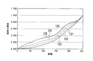
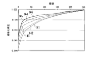
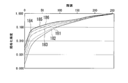
- the horizontal axis indicates gradation and the vertical axis indicates normalized luminance.
- Reference numeral 122 denotes a gamma characteristic at a polar angle ⁇ : 15 °.
- Reference numeral 123 indicates a gamma characteristic at a polar angle ⁇ of 30 °.
- Reference numeral 124 indicates a gamma characteristic at a polar angle ⁇ of 45 °.
- Reference numeral 125 denotes a gamma characteristic at a polar angle ⁇ : 60 °.
- Reference numeral 126 denotes a gamma characteristic at a polar angle ⁇ : 75 °. As can be seen from FIG. 18, the gamma characteristic changes depending on the polar angle ⁇ .
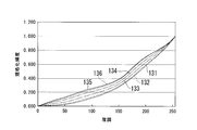
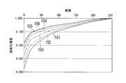
- the horizontal axis represents gradation and the vertical axis represents normalized luminance.
- Reference numeral 132 denotes a gamma characteristic at a polar angle ⁇ : 15 °.
- Reference numeral 133 indicates a gamma characteristic at a polar angle ⁇ of 30 °.
- Reference numeral 134 denotes a gamma characteristic at a polar angle ⁇ : 45 °.
- Reference numeral 135 denotes a gamma characteristic at a polar angle ⁇ : 60 °.
- Reference numeral 136 indicates a gamma characteristic at a polar angle ⁇ : 75 °. It can be seen that the change in the gamma characteristic depending on the polar angle ⁇ is smaller than that of the multi-pixel driving liquid crystal display device having no light control member shown in FIG. In particular, it can be seen that the gamma characteristic at a polar angle ⁇ of 30 ° or more approaches the gamma characteristic at a polar angle ⁇ of 0 °. From this, it can be seen that the color change when the liquid crystal display device 1 is viewed from an oblique direction at an azimuth angle ⁇ of 0 ° is alleviated.
- the present invention is not limited to the multi-pixel driving method used in this embodiment, and other multi-pixel driving methods can be applied to this embodiment.
- the pixel configurations described in JP-A-2006-48055, JP-A-2006-133777, JP-A-2009-199067, and International Publication No. 2008/18552 may be used.
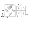
- FIG. 20 is a schematic diagram showing an arrangement relationship between the pixel 50 including the VA mode liquid crystal included in the liquid crystal display device 1 and the light control member 9A.
- the light control member 9A is disposed on the pixel 50.
- the pixel 50 and the light control member 9A are shown in parallel in FIG.
- the pixel 50 in the present embodiment employs a four-domain VA in which one pixel 50 is divided into a first domain 50a, a second domain 50b, a third domain 50c, and a fourth domain 50d. Yes.
- the polarization axis of the first polarizing plate 3 is the azimuth angle ⁇ : 0 ° -180 °.
- the polarization axis of the second polarizing plate 7 is set to the azimuth angle ⁇ : 90 ° -270 ° direction.
- the director of the liquid crystal molecules 51 included in the first domain 50a is inclined such that the polar angle ⁇ at the azimuth angle ⁇ : 45 ° is larger than 0 °.
- the liquid crystal molecules 51 have an azimuth angle ⁇ of 45 ° and a polar angle of 90 ° at the center in the thickness direction of the liquid crystal layer 11 when a voltage is applied. Tilt down closer to °.
- the director of the liquid crystal molecules 51 included in the second domain 50b is inclined such that the polar angle ⁇ at the azimuth angle ⁇ : 135 ° is larger than 0 °.
- the liquid crystal molecules 51 have an azimuth angle ⁇ : 135 ° and a polar angle of 90 ° at the center in the thickness direction of the liquid crystal layer 11 when a voltage is applied. Tilt down closer to °.
- the director of the liquid crystal molecules 51 included in the third domain 50c is inclined so that the polar angle ⁇ at the azimuth angle ⁇ : 225 ° is larger than 0 °.
- the liquid crystal molecules 51 have an azimuth angle ⁇ : 225 ° and a polar angle of 90 at the center in the thickness direction of the liquid crystal layer 11 when a voltage is applied. Tilt down closer to °.
- the director of the liquid crystal molecules 51 included in the fourth domain 50d is inclined such that the polar angle ⁇ at the azimuth angle ⁇ : 315 ° is larger than 0 °.
- the liquid crystal molecules 51 have an azimuth angle ⁇ : 315 ° and a polar angle of 90 at the center in the thickness direction of the liquid crystal layer 11 when a voltage is applied. Tilt down closer to °.
- the light control member 9 ⁇ / b> A of the present embodiment is provided with a plurality of light shielding layers 40 ⁇ / b> K that are scattered on one surface of the base material 39.
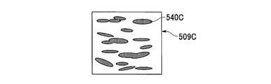
- the planar shape of the light shielding layer 40K viewed from the normal direction of the substrate 39 is an elongated ellipse.
- the light shielding layer 40K has an anisotropic shape having a major axis and a minor axis.
- the ratio of the major axis dimension to the ellipse minor axis dimension is, for example, 1.1 or more and 2.5 or less.
- the major axis of the light shielding layer 40K is, for example, 20 ⁇ m, and the minor axis of the light shielding layer 40K is, for example, 10 ⁇ m.
- the ratio of the length of the short axis to the length of the long axis is approximately equal in each light shielding layer 40K.
- the major axis direction of the ellipse that forms the planar shape of each light shielding layer 40K is generally an azimuth angle ⁇ : 45 ° -225. ° direction or azimuth angle ⁇ : 135 ° -315 ° direction.
- the ratio of the light shielding layer 40K in which the major axis direction is substantially aligned in the direction of azimuth angle ⁇ : 45 ° to 225 ° and the light shielding layer 40K in which the major axis direction is substantially aligned in the direction of azimuth angle ⁇ : 135 ° to 315 ° is approximately 1: 1.
- the major axis direction of the light shielding layer 40K, the polarization axis of the first polarizing plate 3, and the polarization axis of the second polarizing plate 7 are different from each other in the azimuth angle ⁇ by 45 °.
- the major axis direction of the light shielding layer 40K is substantially aligned with the direction of the azimuth angle ⁇ : 45 ° to 225 °, considering the direction of the reflection surface 41c of the light diffusion portion 41, of the reflection surfaces 41c of the light diffusion portion 41, The ratio of the reflective surface 41c along the azimuth angle ⁇ : 45 ° -225 ° direction is larger than the ratio of the reflective surface 41c along the azimuth angle ⁇ : 135 ° -315 ° direction.
- the azimuth angle phi 45 ° -225 azimuth reflected by the reflection surface 41c along ° direction phi: Light L A to diffuse 135 ° -315 ° direction, along the 135 ° -315 ° direction reflected It becomes larger than the light L B to diffuse reflected by the surface 41c to 45 ° -225 ° direction.
- the major axis direction of the light shielding layer 40K is substantially aligned with the direction of the azimuth angle ⁇ : 135 ° to 315 °, considering the direction of the reflection surface 41c of the light diffusion portion 41, of the reflection surfaces 41c of the light diffusion portion 41, The ratio of the reflection surface 41c along the azimuth angle ⁇ : 135 ° -315 ° direction is larger than the ratio of the reflection surface 41c along the azimuth angle ⁇ : 45 ° -225 ° direction.
- the azimuth angle phi 135 ° -315 azimuth reflected by the reflection surface 41c along ° direction phi: 45 ° -225 light L A to diffuse ° direction, reflected along the 45 ° -225 ° direction It becomes larger than the light L B to diffuse reflected by the surface 41c to 135 ° -315 ° direction.
- the azimuth angle directions with relatively strong light diffusibility of the light control member 9A are the azimuth angle ⁇ : 45 ° -225 ° direction and the azimuth angle ⁇ : 135 ° -315 ° direction.
- the light diffusibility of the light control member 9 in the direction of the azimuth angle ⁇ : 0 ° -180 ° which is the polarization axis of the first polarizing plate 3 and the polarization axis of the second polarizing plate 7 is relatively low.
- the light diffusibility of the light control member 9A has line symmetry with respect to the axis of the azimuth angle ⁇ : 45 ° -225 °.
- the light control member 9A is also applied to the azimuth angle ⁇ : 0 ° -180 ° direction axis, the azimuth angle ⁇ : 90 ° -270 ° direction axis, and the azimuth angle ⁇ : 135 ° -315 ° direction axis.
- the light diffusivity has a line symmetry.
- the light diffusibility having line symmetry with respect to a plurality of axes is referred to as having light diffusivity having two or more axes.
- the horizontal axis indicates the gradation
- the vertical axis indicates the normalized luminance.
- reference numeral 141 indicates a gamma characteristic at a polar angle ⁇ : 0 °.
- Reference numeral 142 denotes a gamma characteristic at a polar angle ⁇ : 15 °.
- Reference numeral 143 indicates a gamma characteristic at a polar angle ⁇ of 30 °.
- Reference numeral 144 denotes a gamma characteristic at a polar angle ⁇ : 45 °.
- Reference numeral 145 indicates a gamma characteristic at a polar angle ⁇ : 60 °.
- Reference numeral 146 indicates a gamma characteristic at a polar angle ⁇ : 75 °.
- FIG. 22 shows gamma characteristics when the polar angle ⁇ is changed at the azimuth angle ⁇ : 315 ° of the liquid crystal display device of the comparative example.
- the horizontal axis indicates gradation and the vertical axis indicates normalized luminance.
- Reference numeral 152 denotes a gamma characteristic at a polar angle ⁇ : 15 °.
- Reference numeral 153 indicates a gamma characteristic at a polar angle ⁇ of 30 °.
- Reference numeral 154 indicates a gamma characteristic at a polar angle ⁇ : 45 °.
- Reference numeral 155 indicates a gamma characteristic at a polar angle ⁇ : 60 °.
- Reference numeral 156 represents a gamma characteristic at a polar angle ⁇ : 75 °.
- the gamma characteristic at the azimuth angle ⁇ of 0 ° of the liquid crystal display device of the comparative example shown in FIG. 21 Compared with the gamma characteristic at the azimuth angle ⁇ of 0 ° of the liquid crystal display device of the comparative example shown in FIG. 21, the gamma characteristic at the azimuth angle ⁇ of 315 ° of the comparative example of FIG. It can be seen that at low gradations below the tone, it varies greatly depending on the polar angle. Specifically, the normalized luminance value increases as the polar angle increases. That is, when the observer's viewpoint is tilted so that the polar angle ⁇ becomes large at the azimuth angle ⁇ : 315 °, it can be seen that the low gradation display looks white. As shown in FIG. 22, it can be seen that the image appears to float even at the 0th gradation.
- the low gradation display is white in the liquid crystal display device of the comparative example. You can see that it looks floating.
- the horizontal axis indicates gradation and the vertical axis indicates normalized luminance.
- reference numeral 161 indicates a gamma characteristic at a polar angle ⁇ : 0 °.
- Reference numeral 162 denotes a gamma characteristic at a polar angle ⁇ : 15 °.
- Reference numeral 163 indicates a gamma characteristic at a polar angle ⁇ of 30 °.
- Reference numeral 164 indicates a gamma characteristic at a polar angle ⁇ : 45 °.
- Reference numeral 165 indicates a gamma characteristic at a polar angle ⁇ : 60 °.
- Reference numeral 166 indicates a gamma characteristic at a polar angle ⁇ : 75 °.
- a light control member in which the inclination angle of the light diffusion portion is 80 ° and the ratio of the occupied area of the light shielding layer 40 is 30% is used.
- the change in the gamma characteristic depending on the polar angle ⁇ of the liquid crystal display device 1 of the first embodiment is reduced.
- the gamma characteristic with a polar angle ⁇ of 30 ° or more approaches the gamma characteristic with a polar angle ⁇ of 0 °.
- FIG. 24 shows the gamma characteristics when the polar angle ⁇ is changed at the azimuth angle ⁇ : 315 ° of the liquid crystal display device 1 of the first embodiment.
- the horizontal axis indicates gradation, and the vertical axis indicates normalized luminance.
- reference numeral 171 indicates a gamma characteristic when the polar angle ⁇ is 0 °.
- Reference numeral 172 indicates a gamma characteristic at a polar angle ⁇ : 15 °.
- Reference numeral 173 indicates a gamma characteristic at a polar angle ⁇ of 30 °.
- Reference numeral 174 indicates a gamma characteristic at a polar angle ⁇ : 45 °.
- Reference numeral 175 indicates a gamma characteristic at a polar angle ⁇ : 60 °.
- Reference numeral 176 indicates a gamma characteristic at a polar angle ⁇ : 75 °.
- a light control member in which the inclination angle of the light diffusion portion is 80 ° and the ratio of the occupied area of the light shielding layer 40 is 30% is used.
- the change in the gamma characteristic depending on the polar angle ⁇ is smaller as shown in FIG. I understand that. Specifically, the gamma characteristic with a polar angle ⁇ of 30 ° or more approaches the gamma characteristic with a polar angle ⁇ of 0 °. In particular, it can be seen that the low-gradation gamma characteristic of 25 gradations or less is improved so as to approach the gamma characteristic of the polar angle ⁇ : 0 ° at a polar angle ⁇ of 45 ° or more. From this, it can be said that the whitening of the low gradation display that occurs when the observer's viewpoint is tilted so as to increase the polar angle ⁇ is improved.
- the horizontal axis represents gradation and the vertical axis represents normalized luminance.
- reference numeral 181 indicates a gamma characteristic when the polar angle ⁇ is 0 °.
- Reference numeral 182 indicates a gamma characteristic at a polar angle ⁇ : 15 °.
- Reference numeral 183 indicates a gamma characteristic at a polar angle ⁇ of 30 °.
- Reference numeral 184 indicates a gamma characteristic at a polar angle ⁇ : 45 °.
- Reference numeral 185 indicates a gamma characteristic at a polar angle ⁇ : 60 °.
- Reference numeral 186 indicates a gamma characteristic at a polar angle ⁇ : 75 °.
- a light control member in which the inclination angle of the light diffusion portion is 80 ° and the ratio of the occupied area of the light shielding layer 40 is 30% is used.
- the long axis dimension of the light shielding layer is 20 ⁇ m, and the short axis dimension is 10 ⁇ m.
- the change in the gamma characteristic depending on the polar angle ⁇ of the liquid crystal display device 1 of this embodiment shown in FIG. 25 is smaller than that of the liquid crystal display device of the comparative example shown in FIG. Specifically, the gamma characteristic with a polar angle ⁇ of 30 ° or more approaches the gamma characteristic with a polar angle ⁇ of 0 °.
- the gamma characteristic of the liquid crystal display device 1 of the present embodiment shown in FIG. 25 does not change much compared to the gamma characteristic of the liquid crystal display device 1 of the first embodiment shown in FIG.
- FIG. 26 shows the gamma characteristics when the polar angle ⁇ is changed at the azimuth angle ⁇ : 315 ° of the liquid crystal display device 1 of the present embodiment.
- the horizontal axis indicates gradation and the vertical axis indicates normalized luminance.
- reference numeral 191 indicates a gamma characteristic when the polar angle ⁇ is 0 °.
- Reference numeral 192 indicates a gamma characteristic at a polar angle ⁇ : 15 °.
- Reference numeral 193 indicates a gamma characteristic at a polar angle ⁇ of 30 °.
- Reference numeral 194 indicates a gamma characteristic at a polar angle ⁇ : 45 °.
- Reference numeral 195 indicates a gamma characteristic at a polar angle ⁇ : 60 °.
- Reference numeral 196 indicates a gamma characteristic at a polar angle ⁇ : 75 °.
- a light control unit in which the inclination angle of the light diffusion unit is 80 ° and the ratio of the occupied area of the light shielding layer 40 is 30% is used.
- the long axis dimension of the light shielding layer is 20 ⁇ m, and the short axis dimension is 10 ⁇ m.
- the change in the gamma characteristic depending on the polar angle ⁇ of the liquid crystal display device 1 of this embodiment shown in FIG. 26 is smaller than that of the liquid crystal display device of the comparative example shown in FIG. Specifically, the gamma characteristic with a polar angle ⁇ of 30 ° or more approaches the gamma characteristic with a polar angle ⁇ of 0 °.
- the change in the gamma characteristic depending on the polar angle ⁇ is smaller in the liquid crystal display device 1 of the present embodiment shown in FIG. 26 than in the display device of the first embodiment shown in FIG.
- further improvement in gamma characteristics is observed at polar angles ⁇ : 60 ° or more. From this, it can be said that the whitening of the low gradation display that occurs when the observer's viewpoint is tilted so as to increase the polar angle ⁇ is improved.
- the reason why the viewing angle characteristic at the azimuth angle ⁇ : 315 ° of the liquid crystal display device 1 of this embodiment is improved as compared with the liquid crystal display device 1 of the first embodiment is as follows.
- the light control member 9A of the present embodiment has relatively high light diffusibility in the azimuth angle directions of the azimuth angle ⁇ : 45 ° -225 ° direction and the azimuth angle ⁇ : 135 ° -315 ° direction. That is, more light is mixed in the azimuth angle ⁇ : 45 ° -225 ° direction and the azimuth angle ⁇ : 135 ° -315 ° direction.
- the azimuth angle ⁇ : 45 ° -225 ° direction and the azimuth angle ⁇ : 135 ° -315 ° direction have low viewing angle characteristics for low gradation display in the liquid crystal display device, as can be seen from the result of the comparative example of FIG.
- the azimuth angle ⁇ In the present embodiment, the azimuth angle ⁇ having a low viewing angle characteristic of the low gradation display of the liquid crystal display device is matched with the azimuth angle ⁇ having a relatively strong light diffusibility of the light control member 9A. As a result, the light emitted in a direction with a low azimuth angle ⁇ and a different polar angle ⁇ is mixed and averaged. As a result, viewing angle characteristics depending on the polar angle ⁇ are improved.
- the long axis of the light-shielding part 40K of the present embodiment is along the azimuth angle ⁇ : 45 ° -225 ° direction or the azimuth angle ⁇ : 135 ° -315 ° direction, and the long axis is the azimuth angle ⁇ : 45 °- This is because the ratio of the light shielding layer 40K in the 225 ° direction to the light shielding layer 40K in which the major axis is in the direction of azimuth ⁇ : azimuth ⁇ : 135 ° to 315 ° is approximately 1: 1.
- the azimuth angle direction with relatively strong diffusibility of the light control member 9A is the azimuth angle ⁇ : 45 ° -225 ° direction and the azimuth angle ⁇ : 135 ° -315 ° direction. Therefore, light incident on the light control member 9 at different polar angles ⁇ is mixed by the light control member 9 in the azimuth angle ⁇ : 45 ° -225 ° direction and the azimuth angle ⁇ : 135 ° -315 ° direction.
- improving the viewing angle characteristics in low gradation display as in this embodiment is effective in improving the display performance of the liquid crystal display device. It can be said.
- a light control member 9A is arranged on the light emission side of the liquid crystal panel 2.
- light incident on the light control member 9A at different polar angles ⁇ is mixed by the light control member 9A.
- the variation in the luminance change depending on the polar angle ⁇ is averaged, and as a result, the change in the gamma characteristic depending on the polar angle ⁇ is alleviated.
- FIGS. 27A to 27F The basic configuration of the liquid crystal display device of this embodiment is the same as that of the seventh embodiment, and is different from the seventh embodiment in that the shape of the light shielding layer in the light control member 9A is inscribed in an ellipse. Therefore, in this embodiment, the description of the basic configuration of the liquid crystal display device is omitted, and the light shielding layer is described.
- FIGS. 27A to 27F are plan views of the light shielding layer of the present embodiment. As shown in FIGS. 27A to 27F, the shape of the light shielding layer of the present embodiment is inscribed in an ellipse.
- the shape of the light shielding layer 440A shown in FIG. 27A is a quadrilateral inscribed in an ellipse.
- the shape of the light shielding layer 440B shown in FIG. 27B is a hexagon inscribed in an ellipse.
- the shape of the light shielding layer 440C illustrated in FIG. 27C is an octagon inscribed in an ellipse.
- the shape of the light shielding layer 440D shown in FIG. 27D is a triangle inscribed in an ellipse.
- the shape of the light shielding layer 440E shown in FIG. 27E is a decagon inscribed in an ellipse.
- the shape of the light shielding layer 440F illustrated in FIG. 27F is a figure inscribed in an ellipse.
- the central portion of the light shielding layer 440F is thinner than the portion inscribed in the ellipse.
- the major axis direction of the light shielding layers 440A to 440F, the polarization axis of the first polarizing plate 3, and the polarization axis of the second polarizing plate 7 are different from each other in the azimuth angle ⁇ by 45 °.
- the ninth embodiment of the present invention will be described below with reference to FIGS. 28A to 28D.
- the basic configuration of the liquid crystal display device of this embodiment is the same as that of the seventh embodiment, and the configuration of the light shielding layer in the light control member is different from that of the seventh embodiment. Therefore, in this embodiment, description of the basic structure of a liquid crystal display device is abbreviate
- FIGS. 28A to 28D are plan views of the light control member of this embodiment. As shown in FIGS. 28A to 28D, the light control member of this embodiment differs from the light control member of the first embodiment in the configuration of the light shielding layer.
- the ratio of the length of the short axis to the length of the long axis is approximately equal in each light shielding layer 40K.
- the light control member 509A shown in FIG. 28A includes a light shielding layer 540A having a different ratio of the length of the short axis to the length of the long axis.
- the major axis direction of each light shielding layer 40 is arranged in the direction of the azimuth angle ⁇ : 90 ° -270 °.
- the major axis of a part of the light shielding layers 540B among the plurality of light shielding layers 540B is directed in a direction different from the major axes of the other light shielding layers 540B.
- all of the plurality of light shielding layers 40K are arranged in a scattered manner.
- a part of the light shielding layers 540C among the plurality of light shielding layers 540C is connected to a part of the other light shielding layers 540C.
- the shapes of the plurality of light shielding layers 40 are all elliptical.
- the shape of a part of the light shielding layers 540D among the plurality of light shielding layers 540D is rectangular.
- each light shielding layer 40B is a rhombus.
- the two diagonal lines of the rhombus substantially coincide with the polarization axes of the first polarizing plate 3 and the second polarizing plate 7, respectively. If the longer one of the two diagonal lines of the rhombus is taken as the major axis, the ratio of the light shielding layer 40B whose major axis substantially coincides with the polarization axis of the first polarizing plate 3, and the major axis being the polarization axis of the second polarizing plate 7.
- the ratio of the light shielding layers 40B that are substantially coincident may be approximately 1: 1.
- the planar shape of the light shielding layer 40B of the present embodiment is a rhombus with an acute angle of 30 °. Further, the reflection surface 41c of the light diffusion portion 41 has an inclination angle of 85 °. The operation of the light control member having the light shielding layer 40B will be described below.
- FIG. 30A is a plan view of the light control member.
- the polarization axes of the first polarizing plate 3 and the second polarizing plate 7 coincide with the y-axis and the x-axis, respectively.
- the light L4 emitted through the second polarizing plate 7 is reflected by the light reflecting surface 41c.
- the reflection angle of the light L4 is approximately 45 ° when viewed from the normal direction of the xy plane.
- FIG. 30B is a diagram illustrating the reflection of the light L3 in the case of the reflecting surface X having no inclination angle.
- FIG. 30C is a diagram illustrating the reflection of the light L4 in the case of the reflecting surface 41c when the inclination angle is 85 °.
- the light reflecting surface 41c of this embodiment has an inclination angle of 85 ° as shown in FIG. 30C. Therefore, even if the light L4 passes through the coordinates (x 1 , y 1 , 0) similarly to the light L3 and enters the reflecting surface 41c, the reflected light does not have the same optical path as that of L3. The angle of reflection spreads when viewed. Specifically, the light L4 is reflected in a direction of 45 ° with respect to the x-axis as shown in FIG. 30A.
- FIG. 31 is a graph plotting ⁇ u′v ′ values at various azimuth angles at a polar angle of 60 °.
- ⁇ u′v ′ is the u′v ′ chromaticity of the color that can be seen at a certain polar angle and azimuth when the front color is displayed and the u′v ′ uniform color space of the u′v ′ chromaticity in the front direction. Is the distance between coordinates.
- the Macbeth chart color No. 13 shows the ⁇ u′v ′ characteristic when “Blue” is displayed.
- the solid line indicates the ⁇ u′v ′ characteristic of the liquid crystal display device using the light control member in the present embodiment.
- the alternate long and short dash line indicates the ⁇ u′v ′ characteristic in the liquid crystal display device of the first embodiment.
- the broken line indicates the ⁇ u′v ′ characteristic in the liquid crystal display device (comparative example) that does not use the light control member.
- the ratio of the light-diffusion part 41 in the light control member of this embodiment and 1st Embodiment is 70%.
- ⁇ u′v ′ is small at azimuth angles of 45 °, 135 °, 225 °, and 315 °.
- ⁇ u′v ′ is large at azimuth angles of 0 °, 90 °, 180 °, and 270 °, which are shifted by 45 ° from a small azimuth angle.
- the ⁇ u′v ′ characteristic has an azimuth angle dependency, and the difference in color between when viewed from the front and when viewed obliquely at approximately azimuth angles of 0 °, 90 °, 180 °, and 270 °. It can be said that it is big.
- the ⁇ u′v ′ characteristics are improved at all azimuth angles and the azimuth angle dependency is also improved as in the liquid crystal display device of the first embodiment.
- ⁇ u′v ′ is larger, and ⁇ u ′ is larger at azimuth angles of 0 °, 90 °, 180 °, and 270 °. It can be seen that the v ′ characteristic is improved.
- the light incident on the reflection surface 41c of the light diffusing unit 41 is reflected in directions different in azimuth angle by 45 °.
- light having azimuth angles of 45 °, 135 °, 225 °, and 315 °, which had a small ⁇ u′v ′ passes through the light control member of the present embodiment, and thus has a direction different by 45 °, that is, ⁇ u′v ′. It is injected to the large azimuth.
- the light having a small color change is distributed in the azimuth direction where the color change is large, thereby reducing the variation in ⁇ u′v ′ as a whole.
- the liquid crystal display devices of the first to tenth embodiments described above can be applied to various electronic devices.
- an electronic apparatus including the liquid crystal display device according to the first to tenth embodiments will be described with reference to FIGS. 32 to 34.
- FIG. The liquid crystal display devices of the first to tenth embodiments described above can be applied to, for example, the mobile phone shown in FIG.
- a cellular phone 240 illustrated in FIG. 32 includes a voice input unit 241, a voice output unit 242, an antenna 243, an operation switch 244, a display unit 245, a housing 246, and the like.
- the display unit 245 the liquid crystal display devices of the first to tenth embodiments described above can be suitably applied.
- liquid crystal display devices of the first to tenth embodiments described above can be applied to, for example, a thin television shown in FIG.
- a thin television 250 illustrated in FIG. 33 includes a display portion 251, a speaker 252, a cabinet 253, a stand 254, and the like.
- the display unit 251 the liquid crystal display devices of the first to tenth embodiments described above can be suitably applied.
- an image with a small viewing angle dependency can be displayed.
- the liquid crystal display devices of the first to tenth embodiments described above can be applied to, for example, a notebook computer shown in FIG.
- a notebook computer 270 illustrated in FIG. 34 includes a display portion 271, a keyboard 272, a touch pad 273, a main switch 274, a camera 275, a recording medium slot 276, a housing 277, and the like.
- the display unit 271 the liquid crystal display devices of the first to tenth embodiments described above can be suitably applied.
- an antireflection layer it is also possible to provide at least one of an antireflection layer, a polarizing filter layer, an antistatic layer, an antiglare treatment layer, and an antifouling treatment layer on the viewing side of the base material of the light control member in the above embodiment. good.
- the light diffusing portion or the space portion has an elliptical truncated cone shape, but may have other shapes.
- the inclination angle of the reflection surface of the light diffusing portion is not necessarily symmetric about the optical axis.
- the shape of the light diffusing part is an elliptical truncated cone as in the above embodiment, the angle of inclination of the reflecting surface of the light diffusing part is line symmetric about the optical axis, and therefore line symmetric about the optical axis. Angle distribution is obtained.
- the inclination angle of the reflection surface of the light diffusing unit may be asymmetric.
- each component of the liquid crystal display device is not limited to the above-described embodiment, and can be changed as appropriate.
- a polarizing plate and a retardation plate are arranged outside the liquid crystal panel.
- a polarizing layer and a retardation layer are provided inside a pair of substrates constituting the liquid crystal panel. It may be formed.
- Some aspects of the present invention can be used in a liquid crystal display device.
Landscapes
- Physics & Mathematics (AREA)
- Nonlinear Science (AREA)
- General Physics & Mathematics (AREA)
- Optics & Photonics (AREA)
- Mathematical Physics (AREA)
- Chemical & Material Sciences (AREA)
- Crystallography & Structural Chemistry (AREA)
- Spectroscopy & Molecular Physics (AREA)
- Liquid Crystal (AREA)
Abstract
液晶装置は、第1の垂直配向膜を有する第1の基板と、第2の垂直配向膜を有する第2の基板と、第1の垂直配向膜と第2の垂直配向膜との間に挟持された負の誘電異方性を有する液晶層と、液晶層の光入射側に配置された第1の偏光板と、液晶層の光射出側に配置された第2の偏光板と、を含む液晶パネルと、液晶パネルの光入射側に配置され、液晶パネルに向けて光を射出する照明装置と、液晶パネルの光射出側に配置され、液晶パネルから射出された光を液晶パネルの法線方向から見た方位角方向および極角方向に拡散させて光の射出方向を制御する光制御部材と、を備え、液晶パネルが、表示の基本単位となる画素を複数備え、画素が、電圧印加時の液晶層の厚さ方向中央部の液晶分子のダイレクタの方向もしくは向きが異なる複数の領域を有する。
Description
本発明は、液晶表示装置に関する。
本願は、2012年12月18日に、日本に出願された特願2012-275767号に基づき優先権を主張し、その内容をここに援用する。
本願は、2012年12月18日に、日本に出願された特願2012-275767号に基づき優先権を主張し、その内容をここに援用する。
携帯電話機等をはじめとする携帯型電子機器、もしくはテレビジョン、パーソナルコンピューター等のディスプレイとして、液晶表示装置が広く用いられている。一般に、液晶表示装置は、表示画面を正面から見たときに優れた表示特性を発揮する。一方、表示画面を斜め方向から見たときにはコントラストが低下し視認性が悪くなりやすい。あるいは、階調表示において明るさが逆転する階調反転等が起こることがある。このため、良好な視認性で画面を観察可能な視野角範囲を広げる様々な手法が提案されている。
例えば、特許文献1は、視野角特性が良好なVA(Vertically Alignment)モードの液晶表示装置及びMVA(Multi-domain Vertical Alignment)モードの液晶表示装置を開示している。
一画素のドメイン数を4つとしたVAモードの液晶表示装置の場合、それぞれのドメインに含まれる液晶分子の長軸の平均方向(ダイレクタ)は、電圧印加時において、方位角が90°ずつ異なる。複数のドメインに分割されていないVAモードの液晶表示装置と比較して、4つのドメインを有するVAモードの液晶表示装置は、視野角特性が向上している。具体的には、4つのドメインを有するVAモードの液晶表示装置では、上下左右方向から斜めに液晶表示装置を見た場合、ガンマ特性(階調-輝度特性)の変化が小さい。しかしながら、4つのドメインを有するVAモードの液晶表示装置においても、上下左右方向から斜めに液晶表示装置を見た場合と、正面から液晶表示装置を見た場合とでは、表示画像の色変化が生じる。
本発明は、上記の課題を解決するためになされたものであって、視野角依存性の小さい液晶表示装置の提供を目的とする。
本発明の一態様における液晶表示装置は、第1の垂直配向膜を有する第1の基板と、第2の垂直配向膜を有する第2の基板と、前記第1の垂直配向膜と前記第2の垂直配向膜との間に挟持された負の誘電異方性を有する液晶層と、前記液晶層の光入射側に配置された第1の偏光板と、前記液晶層の光射出側に配置された第2の偏光板と、を含む液晶パネルと、前記液晶パネルの光入射側に配置され、前記液晶パネルに向けて光を射出する照明装置と、前記液晶パネルの光射出側に配置され、前記液晶パネルから射出された光を前記液晶パネルの法線方向から見た方位角方向および極角方向に拡散させて前記光の射出方向を制御する光制御部材と、を備え、前記液晶パネルが、表示の基本単位となる画素を複数備え、前記画素が、電圧印加時の前記液晶層の厚さ方向中央部の液晶分子のダイレクタの方向もしくは向きが異なる複数の領域を有する。
本発明の一態様における液晶表示装置において、前記光制御部材が、光透過性を有する基材と、前記基材の第1の面に形成された光拡散部と、前記基材の第1の面のうち前記光拡散部の形成領域以外の領域に形成された遮光部と、を備え、前記光拡散部が、前記基材側に位置する光射出端面と、前記基材側と反対側に位置し前記光射出端面の面積よりも大きい面積の光入射端面と、前記光射出端面と前記光入射端面との間に位置する傾斜面と、を有し、前記光拡散部の前記光入射端面から前記光射出端面までの高さが前記遮光部の高さよりも高く、前記光拡散部が形成されていない領域の光拡散部間の間隙に、前記光拡散部の屈折率よりも小さい屈折率を有する物質が存在していてもよい。
本発明の一態様における液晶表示装置において、前記光制御部材の光散乱特性が、前記液晶パネルの法線方向から見て2軸以上の線対称性を有してもよい。
本発明の一態様における液晶表示装置において、前記基材の法線方向から見た前記遮光部の平面形状が、円形であってもよい。
本発明の一態様における液晶表示装置において、前記基材の法線方向から見た前記遮光部の平面形状が、長軸と短軸とを有する異方性形状であり、前記遮光部が、前記長軸の延在方向および前記短軸の延在方向がそれぞれ異なるように配置された複数の遮光部を含んでもよい。
本発明の一態様における液晶表示装置において、前記遮光部の前記長軸の延在方向および前記短軸の延在方向が、前記複数の領域における前記液晶分子のダイレクタの方向と概ね一致していてもよい。
本発明の一態様における液晶表示装置において、前記平面形状が、楕円形であってもよい。
本発明の一態様における液晶表示装置において、前記平面形状が、楕円に内接する多角形であってもよい。
本発明の一態様における液晶表示装置において、前記光拡散部の前記光入射端面と前記傾斜面とのなす角度が、80°±5°であってもよい。
本発明の一態様における液晶表示装置において、前記基材の前記第1の面の全面積に対する前記遮光部の占有面積の割合が、30%±10%であってもよい。
本発明の一態様における液晶表示装置において、前記第1の垂直配向膜および前記第2の垂直配向膜が、光配向膜であってもよい。
本発明の一態様における液晶表示装置において、前記液晶パネルが、モノラルカラー表示を行ってもよい。
本発明の態様によれば、複雑な回路構造を適用することなく、視野角依存性の小さい液晶表示装置を提供することができる。
[第1実施形態]
以下、本発明の一実施形態について、図1~図9Dを用いて説明する。
本実施形態では、透過型の液晶パネルを備えた液晶表示装置の例を挙げて説明する。
なお、以下の全ての図面においては、各構成要素を見やすくするため、構成要素によって寸法の縮尺を異ならせて示すことがある。
以下、本発明の一実施形態について、図1~図9Dを用いて説明する。
本実施形態では、透過型の液晶パネルを備えた液晶表示装置の例を挙げて説明する。
なお、以下の全ての図面においては、各構成要素を見やすくするため、構成要素によって寸法の縮尺を異ならせて示すことがある。
図1は、本実施形態の液晶表示装置1の断面図である。
本実施形態の液晶表示装置1は、図1に示すように、液晶パネル2と、バックライト8(照明装置)と、光制御部材9(光制御部材)と、を備えている。液晶パネル2は、第1偏光板3と、第1位相差フィルム4(位相差板)と、液晶セル5と、第2位相差フィルム6(位相差板)と、第2偏光板7と、を備えている。図1では、液晶セル5を模式的に図示しているが、その詳細な構造については後述する。
本実施形態の液晶表示装置1は、図1に示すように、液晶パネル2と、バックライト8(照明装置)と、光制御部材9(光制御部材)と、を備えている。液晶パネル2は、第1偏光板3と、第1位相差フィルム4(位相差板)と、液晶セル5と、第2位相差フィルム6(位相差板)と、第2偏光板7と、を備えている。図1では、液晶セル5を模式的に図示しているが、その詳細な構造については後述する。
観察者は、液晶表示装置1の表示画像を光制御部材9を介して見ることになる。以下の説明では、光制御部材9が配置された側を視認側と称する。バックライト8が配置された側を背面側と称する。また、以下の説明において、x軸は、液晶表示装置の画面の水平方向と定義する。y軸は、液晶表示装置の画面の垂直方向と定義する。z軸は、液晶表示装置の厚さ方向と定義する。
本実施形態の液晶表示装置1においては、バックライト8から射出された光を液晶パネル2で変調し、変調した光によって所定の画像や文字等を表示する。また、液晶パネル2から射出された光が光制御部材9を透過すると、射出光の配光分布が光制御部材9に入射する前より広がった状態となって光が光制御部材9から射出される。これにより、観察者は広い視野角を持って表示を視認できる。
以下、液晶パネル2の具体的な構成について説明する。
ここでは、アクティブマトリクス方式の透過型液晶パネルを一例に挙げて説明する。ただし、本実施形態に適用可能な液晶パネルはアクティブマトリクス方式の透過型液晶パネルに限るものではない。本実施形態に適用可能な液晶パネルは、例えば半透過型(透過・反射兼用型)液晶パネルであっても良い。さらには、各画素がスイッチング用薄膜トランジスタ(Thin Film Transistor, 以下、TFTと略記する)を備えていない単純マトリクス方式の液晶パネルであっても良い。
ここでは、アクティブマトリクス方式の透過型液晶パネルを一例に挙げて説明する。ただし、本実施形態に適用可能な液晶パネルはアクティブマトリクス方式の透過型液晶パネルに限るものではない。本実施形態に適用可能な液晶パネルは、例えば半透過型(透過・反射兼用型)液晶パネルであっても良い。さらには、各画素がスイッチング用薄膜トランジスタ(Thin Film Transistor, 以下、TFTと略記する)を備えていない単純マトリクス方式の液晶パネルであっても良い。
図2は、液晶パネル2の縦断面図である。
図2に示すように、液晶セル5は、TFT基板10と、カラーフィルター基板12と、液晶層11と、を有している。TFT基板10は、スイッチング素子基板として機能する。カラーフィルター基板12は、TFT基板10に対向して配置されている。液晶層11は、TFT基板10とカラーフィルター基板12との間に挟持されている。
図2に示すように、液晶セル5は、TFT基板10と、カラーフィルター基板12と、液晶層11と、を有している。TFT基板10は、スイッチング素子基板として機能する。カラーフィルター基板12は、TFT基板10に対向して配置されている。液晶層11は、TFT基板10とカラーフィルター基板12との間に挟持されている。
液晶層11は、TFT基板10と、カラーフィルター基板12と、枠状のシール部材(図示せず)と、によって囲まれた空間内に封入されている。シール部材は、TFT基板10とカラーフィルター基板12とを所定の間隔をおいて貼り合わせる。
本実施形態の液晶パネル2は、例えばVA(Vertical Alignment,垂直配向)モードで表示を行う。
液晶層11には誘電率異方性が負の液晶が用いられる。TFT基板10とカラーフィルター基板12との間には、スペーサー13が配置されている。スペーサー13は球状或いは柱状である。スペーサー13は、TFT基板10とカラーフィルター基板12との間の間隔を一定に保持する。
液晶層11には誘電率異方性が負の液晶が用いられる。TFT基板10とカラーフィルター基板12との間には、スペーサー13が配置されている。スペーサー13は球状或いは柱状である。スペーサー13は、TFT基板10とカラーフィルター基板12との間の間隔を一定に保持する。
図示はしないが、TFT基板10には、複数の画素がマトリクス状に配置されている。
画素は、表示の基本単位である。TFT基板10には、複数のソースバスラインが、互いに平行に延在するように形成されている。TFT基板10には、複数のゲートバスラインが、互いに平行に延在するように形成されている。複数のゲートバスラインは、複数のソースバスラインと直交している。TFT基板10上には、複数のソースバスラインと複数のゲートバスラインとが格子状に形成されている。隣接するソースバスラインと隣接するゲートバスラインとによって区画された矩形状の領域が一つの画素となる。ソースバスラインは、TFT19のソース電極17に接続されている。ゲートバスラインは、TFT19のゲート電極16に接続されている。
画素は、表示の基本単位である。TFT基板10には、複数のソースバスラインが、互いに平行に延在するように形成されている。TFT基板10には、複数のゲートバスラインが、互いに平行に延在するように形成されている。複数のゲートバスラインは、複数のソースバスラインと直交している。TFT基板10上には、複数のソースバスラインと複数のゲートバスラインとが格子状に形成されている。隣接するソースバスラインと隣接するゲートバスラインとによって区画された矩形状の領域が一つの画素となる。ソースバスラインは、TFT19のソース電極17に接続されている。ゲートバスラインは、TFT19のゲート電極16に接続されている。
TFT基板10を構成する透明基板14の液晶層11側の面には、半導体層15、ゲート電極16、ソース電極17、ドレイン電極18等を有するTFT19が形成されている。透明基板14としては、例えばガラス基板を用いることができる。
透明基板14上には、半導体層15が形成されている。半導体層15の材料としては、例えばCGS(Continuous Grain Silicon:連続粒界シリコン)、LPS(Low-temperature Poly-Silicon:低温多結晶シリコン)、α-Si(Amorphous Silicon:非結晶シリコン)等の半導体材料が用いられる。
透明基板14上には、半導体層15を覆うようにゲート絶縁膜20が形成されている。
ゲート絶縁膜20の材料としては、例えばシリコン酸化膜、シリコン窒化膜、もしくはこれらの積層膜等が用いられる。
ゲート絶縁膜20の材料としては、例えばシリコン酸化膜、シリコン窒化膜、もしくはこれらの積層膜等が用いられる。
ゲート絶縁膜20上には、半導体層15と対向するようにゲート電極16が形成されている。ゲート電極16の材料としては、例えばW(タングステン)/TaN(窒化タンタル)の積層膜、Mo(モリブデン)、Ti(チタン)、Al(アルミニウム)等が用いられる。
ゲート絶縁膜20上には、ゲート電極16を覆うように第1層間絶縁膜21が形成されている。第1層間絶縁膜21の材料としては、例えばシリコン酸化膜、シリコン窒化膜、もしくはこれらの積層膜等が用いられる。
第1層間絶縁膜21上には、ソース電極17およびドレイン電極18が形成されている。第1層間絶縁膜21とゲート絶縁膜20とには、コンタクトホール22およびコンタクトホール23が、第1層間絶縁膜21とゲート絶縁膜20とを貫通して形成されている。
ソース電極17は、コンタクトホール22を介して半導体層15のソース領域に接続されている。ドレイン電極18は、コンタクトホール23を介して半導体層15のドレイン領域に接続されている。ソース電極17およびドレイン電極18の材料としては、上述のゲート電極16と同様の導電性材料が用いられる。
ソース電極17は、コンタクトホール22を介して半導体層15のソース領域に接続されている。ドレイン電極18は、コンタクトホール23を介して半導体層15のドレイン領域に接続されている。ソース電極17およびドレイン電極18の材料としては、上述のゲート電極16と同様の導電性材料が用いられる。
第1層間絶縁膜21上には、ソース電極17およびドレイン電極18を覆うように第2層間絶縁膜24が形成されている。第2層間絶縁膜24の材料としては、上述の第1層間絶縁膜21と同様の材料、もしくは有機絶縁性材料が用いられる。
第2層間絶縁膜24上には、画素電極25が形成されている。第2層間絶縁膜24には、コンタクトホール26が第2層間絶縁膜24を貫通して形成されている。画素電極25は、コンタクトホール26を介してドレイン電極18に接続されている。画素電極25は、ドレイン電極18を中継用電極として半導体層15のドレイン領域に接続されている。
画素電極25の材料としては、例えばITO(Indium Tin Oxide、インジウム錫酸化物)、IZO(Indium Zinc Oxide、インジウム亜鉛酸化物)等の透明導電性材料が用いられる。
画素電極25の材料としては、例えばITO(Indium Tin Oxide、インジウム錫酸化物)、IZO(Indium Zinc Oxide、インジウム亜鉛酸化物)等の透明導電性材料が用いられる。
この構成により、ゲートバスラインを通じて走査信号が供給され、TFT19がオン状態となったときに、ソースバスラインを通じてソース電極17に供給された画像信号が、半導体層15、ドレイン電極18を経て画素電極25に供給される。また、なお、TFT19の形態としては、図2に示したトップゲート型TFTであっても良いし、ボトムゲート型TFTであっても良い。
画素電極25を覆うように第2層間絶縁膜24上の全面に第1の垂直配向膜27が形成されている。第1の垂直配向膜27は、液晶層11を構成する液晶分子を垂直配向させる配向規制力を有している。第1の垂直配向膜27は、いわゆる垂直配向膜である。本実施形態では、光配向技術を用いて第1の垂直配向膜27に配向処理を施している。つまり、本実施形態では第1の垂直配向膜27として光配向膜を用いている。
一方、カラーフィルター基板12を構成する透明基板29の液晶層11側の面には、ブラックマトリクス30、カラーフィルター31、平坦化層32、対向電極33、第2の垂直配向膜34が順次形成されている。
ブラックマトリクス30は、画素間領域において光の透過を遮断する機能を有する。ブラックマトリクス30は、例えば、Cr(クロム)やCr/酸化Crの多層膜等の金属、もしくはカーボン粒子を感光性樹脂に分散させたフォトレジストで形成されている。
カラーフィルター31には、赤色(R)、緑色(G)、青色(B)の各色の色素が含まれている。TFT基板10上の一つの画素電極25に、R,G,Bのいずれか一つのカラーフィルター31が対向して配置されている。なお、カラーフィルター31は、R、G、Bの3色以上の多色構成としても良い。
平坦化層32は、ブラックマトリクス30およびカラーフィルター31を覆う絶縁膜で構成されている。平坦化層32は、ブラックマトリクス30およびカラーフィルター31によってできる段差を緩和して平坦化する機能を有している。
平坦化層32上には対向電極33が形成されている。対向電極33の材料としては、画素電極25と同様の透明導電性材料が用いられる。
対向電極33上の全面に第2の垂直配向膜34が形成されている。第2の垂直配向膜34は、液晶層11を構成する液晶分子を垂直配向させる配向規制力を有している。第2の垂直配向膜34は、いわゆる垂直配向膜である。本実施形態では、光配向技術を用いて第2の垂直配向膜34に配向処理を施している。つまり、本実施形態では第2の垂直配向膜34として光配向膜を用いている。
図1に戻り、照明装置であるバックライト8は、光源36と、導光体37と、を備えている。光源36は、導光体37の端面に配置されている。光源36としては、例えば、発光ダイオード、冷陰極管等が用いられる。
本実施形態のバックライト8は、エッジライト型のバックライトである。
本実施形態のバックライト8は、エッジライト型のバックライトである。
導光体37は、光源36から射出された光を液晶パネル2に導く機能を有する。導光体37の材料としては、例えば、アクリル樹脂等の樹脂材料が用いられる。
光源36から導光体37の端面に入射した光は、導光体37の内部を全反射して伝播し、導光体37の上面(光射出面)から概ね均一な強度で射出される。図示はしないが、導光体37の上面には、散乱シート及びプリズムシートが配置されており、導光体37の下面には、散乱シートが配置されている。導光体37の上面から射出された光は、散乱シートにより散乱した後、プリズムシートによって集光され、概ね平行化されて射出される。
散乱シートとしては、白色PETを用いてもよい。プリズムシートとしては、例えば、住友3M社製のBEF(商品名)を用いてもよい。
散乱シートとしては、白色PETを用いてもよい。プリズムシートとしては、例えば、住友3M社製のBEF(商品名)を用いてもよい。
本実施形態において、バックライト8は指向性を有する必要はない。本実施形態のバックライト8としては、光の射出方向を制御して、指向性がある程度緩やかに設定されたバックライト(以下、通常バックライトと称することがある)を用いる。なお本実施形態において、バックライト8が指向性を有していても構わない。
バックライト8と液晶セル5との間には、第1偏光板3が設けられている。第1偏光板3は、偏光子として機能する。液晶セル5と光制御部材9との間には、第2偏光板7が設けられている。第2偏光板7は、偏光子として機能する。第1偏光板3の透過軸と第2偏光板7の透過軸とは、クロスニコルの配置となっている。
第1偏光板3と液晶セル5との間には、光の位相差を補償するための第1位相差フィルム4が設けられている。第2偏光板7と液晶セル5との間には、光の位相差を補償するための第2位相差フィルム6が設けられている。
本実施形態の位相差フィルム(第1位相差フィルム4、第2位相差フィルム6)としては、富士フィルム社製のWVフィルムが用いられる。
次に、光制御部材9について詳細に説明する。
図3は、光制御部材9を視認側から見た斜視図である。図4は、光制御部材9の模式図である。図4において、左側上段は光制御部材9の平面図である。左側下段は、左側上段の平面図のA-A線に沿った断面図である。右側上段は、左側上段の平面図のB-B線に沿った断面図である。
図3は、光制御部材9を視認側から見た斜視図である。図4は、光制御部材9の模式図である。図4において、左側上段は光制御部材9の平面図である。左側下段は、左側上段の平面図のA-A線に沿った断面図である。右側上段は、左側上段の平面図のB-B線に沿った断面図である。
光制御部材9は、図3に示すように、基材39と、複数の遮光層40と、光拡散部41と、を備えている。複数の遮光層40は、基材39の一面(視認側と反対側の面)に形成されている。光拡散部41は、基材39の一面のうち遮光層40の形成領域以外の領域に形成されている。
光制御部材9は、図1に示すように、光拡散部41を第2偏光板7に向け、基材39を視認側に向けて第2偏光板7上に配置される。光制御部材9は、接着剤層43を介して第2偏光板7に固定される。
基材39には、例えばトリアセチルセルロース(TAC)フィルム、ポリエチレンテレフタレート(PET)、ポリカーボネート(PC)、ポリエチレンナフタレート(PEN)、ポリエーテルサルホン(PES)フィルム等の透明樹脂製の基材が好ましく用いられる。基材39は、製造プロセスにおいて、後で遮光層40や光拡散部41の材料を塗布する際の下地となる。基材39は、製造プロセス中の熱処理工程における耐熱性と機械的強度とを備える必要がある。したがって、基材39には、樹脂製の基材の他、ガラス製の基材等を用いても良い。ただし、基材39の厚さは耐熱性や機械的強度を損なわない程度に薄い方が好ましい。その理由は、基材39の厚さが厚くなる程、表示のボヤケが生じる虞があるからである。また、基材39の全光線透過率は、JIS K7361-1の規定で90%以上が好ましい。全光線透過率が90%以上であると、十分な透明性が得られる。
本実施形態では、一例として厚さが100μmの透明樹脂製基材を用いる。
本実施形態では、一例として厚さが100μmの透明樹脂製基材を用いる。
遮光層40は、基材39の主面の法線方向から見てランダムに配置されている。遮光層40は、一例として、ブラックレジスト、黒色インク等の光吸収性および感光性を有する有機材料で構成されている。その他、Cr(クロム)やCr/酸化Crの多層膜等の金属膜を用いても良い。
光拡散部41は、例えばアクリル樹脂やエポキシ樹脂等の光透過性および感光性を有する有機材料で構成されている。また、光拡散部41の全光線透過率は、JIS K7361-1の規定で90%以上が好ましい。全光線透過率が90%以上であると、十分な透明性が得られる。
図4に示すように、光拡散部41は、光射出端面41aと、光入射端面41bと、反射面41cと、を有する。光射出端面41aは、基材39に接する面である。光入射端面41bは、光射出端面41aと対向する面である。反射面41cは、光拡散部41のテーパ状の側面である。反射面41cは、光入射端面41bから入射した光を反射する面である。光入射端面41bの面積は、光射出端面41aの面積よりも大きい。
光拡散部41は、光制御部材9において光の透過に寄与する部分である。光拡散部41に入射した光のうち、光L1は、反射面41cで反射されることなく光射出端面41aから射出される。光拡散部41に入射した光のうち、光L2は、光拡散部41の反射面41cで全反射しつつ、光拡散部41の内部に略閉じこめられた状態で導光し、光射出端面41aから射出される。
光制御部材9は、基材39が視認側に向くように配置される。そのため、光拡散部41の2つの対向面のうち、面積の小さい方の面が光射出端面41aとなる。一方、面積の大きい方の面が光入射端面41bとなる。
光拡散部41の反射面41cの傾斜角度(光入射端面41bと反射面41cとのなす角度)は、80°±5°であってもよく、一例として80°程度である。ただし、光拡散部41の反射面41cの傾斜角度は、光制御部材9から射出する際に、入射光を十分に拡散することが可能な角度であれば、特に限定されない。本実施形態において、光拡散部41の反射面41cの傾斜角度は一定になっている。
光拡散部41の光入射端面41bから光射出端面41aまでの高さは、遮光層40の層厚よりも大きく設定されている。本実施形態の場合、遮光層40の層厚は一例として150nm程度である。光拡散部41の光入射端面41bから光射出端面41aまでの高さは一例として20μm程度である。光拡散部41の反射面41cと遮光層40とにより囲まれた部分は、中空部42となっている。中空部42には空気が存在している。
なお、基材39の屈折率と光拡散部41の屈折率とは略同等であることが望ましい。その理由は、以下による。例えば、基材39の屈折率と光拡散部41の屈折率とが大きく異なる場合を考える。この場合、光入射端面41bから入射した光が光拡散部41から射出する際に、光拡散部41と基材39との界面で不要な光の屈折や反射が生じることがある。この場合、所望の視野角が得られない、射出光の光量が減少する、等の不具合が生じる虞があるからである。
本実施形態の場合、中空部42(光拡散部41の外部)には空気が介在している。そのため、光拡散部41を例えば透明アクリル樹脂で形成したとすると、光拡散部41の反射面41cは透明アクリル樹脂と空気との界面となる。ここで、中空部42を他の低屈折率材料で充填しても良い。しかしながら、光拡散部41の内部と外部との界面の屈折率差は、外部にいかなる低屈折率材料が存在する場合よりも空気が存在する場合が最大となる。
したがって、Snellの法則より、本実施形態の構成においては臨界角が最も小さくなり、光拡散部41の反射面41cで光が全反射する入射角範囲が最も広くなる。その結果、光の損失がより抑えられ、高い輝度を得ることができる。
したがって、Snellの法則より、本実施形態の構成においては臨界角が最も小さくなり、光拡散部41の反射面41cで光が全反射する入射角範囲が最も広くなる。その結果、光の損失がより抑えられ、高い輝度を得ることができる。
本実施形態の光制御部材9は、図4の左側上段に示すように、複数の遮光層40が、基材39の一面に点在して設けられている。基材39の法線方向から見た遮光層40の平面形状は円形である。遮光層40の直径は、例えば15μm程度である。
基材39の全面積に対する遮光層40の占有面積の割合は、例えば30%±10%である。
図4の左側下段、右側上段に示すように、遮光層40の下方に相当する部分が円錐台状の中空部42となる。光制御部材9は複数の中空部42を有している。複数の中空部42以外の部分には、光拡散部41が連なって設けられている。
なお、遮光層40の平面形状は、楕円形、多角形、半円等の形状が含まれていても良い。遮光層40の平面形状は、2軸以上の線対称性を有する形状であることが好ましい。2軸以上の線対称性を有する形状とは、少なくとも2つ以上の線分に対して線対称な形状を指す。例えば、2つの線分に対して線対称な形状として、長方形が挙げられる。なお、円形である場合、線対称の軸は無限にあると捉えられるので、2軸以上の線対称性を有する形状に含まれるものとする。このように遮光層40の平面形状が2軸以上の線対称性を有する形状を有する場合、光制御部材9の光散乱特性は、液晶パネル2の法線方向から見て、2軸以上の線対称性を有する。
また、遮光層40の一部が重なって形成されていても良い。
また、遮光層40の一部が重なって形成されていても良い。
以下に、光制御部材9とVAモードの液晶を組み合わせた場合について説明する。
図5は、極角と方位角の定義を説明するための図である。
ここで、図5に示すように、液晶表示装置1の画面の法線方向Eを基準とした観察者の視線方向Fのなす角度を極角θとする。x軸の正方向(0°方向)を基準とした観察者の視線方向Fを画面上に射影したときの線分Gの方向のなす角度を方位角φとする。
図5は、極角と方位角の定義を説明するための図である。
ここで、図5に示すように、液晶表示装置1の画面の法線方向Eを基準とした観察者の視線方向Fのなす角度を極角θとする。x軸の正方向(0°方向)を基準とした観察者の視線方向Fを画面上に射影したときの線分Gの方向のなす角度を方位角φとする。
図6は、液晶表示装置1の正面図である。
図6に示すように、液晶表示装置1の画面において、水平方向(x軸方向)を方位角φ:0°-180°方向とする。垂直方向(y軸方向)を方位角φ:90°-270°方向とする。なお、本実施形態において、第1偏光板3の透過軸は、方位角φ:90°-270°方向であり、第2偏光板7の透過軸は、方位角φ:0°-180°方向である。
図6に示すように、液晶表示装置1の画面において、水平方向(x軸方向)を方位角φ:0°-180°方向とする。垂直方向(y軸方向)を方位角φ:90°-270°方向とする。なお、本実施形態において、第1偏光板3の透過軸は、方位角φ:90°-270°方向であり、第2偏光板7の透過軸は、方位角φ:0°-180°方向である。
図7に、本実施形態の液晶表示装置1の一画素の電気的な構成を模式的に示す。
画素50は、TFT66および補助容量(CS)72に接続されている。TFT66のゲ-ト電極は、走査線62に接続されている。ソース電極は、信号線64に接続されている。補助容量72は、補助容量配線(CSバス・ライン)74に接続されている。補助容量72は、画素電極68に電気的に接続された補助容量電極と、補助容量配線74に電気的に接続された補助容量対向電極と、これらの間に設けられた絶縁層(不図示)によって形成されている。
図7では、液晶パネル2の法線方向から見た液晶分子51を円錐状に記載している。円錐の頂点は、液晶分子51の背面側(TFT基板側)の端部を意味する。円錐の底面は、液晶分子の視認側(カラーフィルター基板側)の端部を示している。本実施形態において、液晶分子51のダイレクタとは、液晶分子の背面側の端部から、視認側の端部へ向かう方向と定義する。
画素50は、四つのドメイン50a、50b、50c、50dを有する4ドメインVAを採用している。電圧印加時において、第1ドメイン50aに含まれる液晶分子51と、第2ドメイン50bに含まれる液晶分子51と、第3ドメイン50cに含まれる液晶分子51と、第4ドメイン50dに含まれる液晶分子51とは、互いに方位角が90°異なる方向に倒れる。四つのドメイン50a、50b、50c、50dに含まれる液晶分子51については、以下でより詳細に説明する。
図8は、液晶表示装置1に含まれるVAモードの液晶を含む画素50と、光制御部材9との配置関係を示す模式図である。実際には図1に示すように、画素50上に光制御部材9が配置されるが、説明の便宜上、図8では画素50と光制御部材9とを並列して記載している。
画素50に含まれる液晶分子51は、電圧を印加しない状態においてほぼ垂直に配向している。
図8に示すように、第1ドメイン50aに含まれる液晶分子51のダイレクタは、方位角φ:45°の方向を向いており、極角θが0°より大きくなるよう傾いている。このように液晶分子51を配向することにより、第1ドメイン50aにおいて、電圧印加時の液晶層11の厚さ方向において中央部では、液晶分子51が方位角φ:45°でかつ極角が90°に近づくように倒れる。
第2ドメイン50bに含まれる液晶分子51のダイレクタは、方位角φ:135°の方向を向いており、極角θが0°より大きくなるよう傾いている。このように液晶分子51を配向することにより、第2ドメイン50bにおいて、電圧印加時の液晶層11の厚さ方向において中央部では、液晶分子51が方位角φ:135°でかつ極角が90°に近づくように倒れる。
第3ドメイン50cに含まれる液晶分子51のダイレクタは、方位角φ:225°の方向を向いており、極角θが0°より大きくなるよう傾いている。このように液晶分子51を配向することにより、第3ドメイン50cにおいて、電圧印加時の液晶層11の厚さ方向において中央部では、液晶分子51が方位角φ:225°でかつ極角が90°に近づくように倒れる。
第4ドメイン50dに含まれる液晶分子51のダイレクタは、方位角φ:315°の方向を向いており、極角θが0°より大きくなるよう傾いている。このように液晶分子51を配向することにより、第4ドメイン50dにおいて、電圧印加時の液晶層11の厚さ方向において中央部では、液晶分子51が方位角φ:315°でかつ極角が90°に近づくように倒れる。
以上のように、第1~第4ドメイン50a~50dに含まれる液晶分子51は、は、互いに方位角が90°異なる方向に傾いて配向している。よって、第1~第4ドメイン50a~50dに含まれる液晶分子51は、電圧印加時に、互いに方位角が90°異なる方向に倒れる。つまり、方位角φ:0°-180°方向の軸に対して、第1ドメイン50aに含まれる液晶分子51は、第4ドメイン50dに含まれる液晶分子51と線対称となるよう倒れ、第2ドメイン50bに含まれる液晶分子51は、第3ドメイン50cに含まれる液晶分子51と線対称となるよう倒れる。また、方位角φ:90°-270°方向の軸に対して、第1ドメイン50aに含まれる液晶分子51は、第1ドメイン50bに含まれる液晶分子51と線対称となるよう倒れ、第3ドメイン50cに含まれる液晶分子51は、第4ドメイン50dに含まれる液晶分子51と線対称となるよう倒れる。すなわち、液晶表示装置1の法線方向から見て2軸の線対称性を有するように倒れる。なお、第1配光膜27および第2配光膜34近傍の液晶分子51は、第1配光膜27および第2配光膜34に配光が規制されているため、電圧印加時においてもほぼ垂直のままである。
本実施形態では、図8に示すように、液晶パネル2の光射出側に光制御部材9が配置される。その結果、異なる極角θで光制御部材9に入射した光は、光制御部材9により混合される。その結果、極角θに依存した輝度変化のばらつきが平均化され、結果として極角θに依存したガンマ特性変化が緩和される。
このように、4ドメインVA方式を採用した液晶表示装置1に、本実施形態の光制御部材9を組み合わせることにより、視野角特性が改善される。
(液晶表示装置の製造方法)
図9A~図9Dは、光制御部材9の製造工程を、順を追って示す斜視図である。
図9A~図9Dは、光制御部材9の製造工程を、順を追って示す斜視図である。
上記構成の液晶表示装置1を構成する光制御部材9の製造工程を中心に、その製造方法について説明する。
液晶パネル2の製造工程の概略を先に説明する。最初に、TFT基板10とカラーフィルター基板12をそれぞれ作製する。その後、TFT基板10のTFT19が形成された側の面とカラーフィルター基板12のカラーフィルター31が形成された側の面とを対向させて配置する。そして、TFT基板10とカラーフィルター基板12とをシール部材を介して貼り合わせる。その後、TFT基板10とカラーフィルター基板12とシール部材とによって囲まれた空間内に液晶を注入する。このようにしてできた液晶セル5の両面に、光学接着剤等を用いて第1位相差フィルム4、第1偏光板3、第2位相差フィルム6、第2偏光板7をそれぞれ貼り合わせる。以上の工程を経て、液晶パネル2が完成する。
なお、TFT基板10やカラーフィルター基板12の製造方法は常法によれば良く、その説明を省略する。
液晶パネル2の製造工程の概略を先に説明する。最初に、TFT基板10とカラーフィルター基板12をそれぞれ作製する。その後、TFT基板10のTFT19が形成された側の面とカラーフィルター基板12のカラーフィルター31が形成された側の面とを対向させて配置する。そして、TFT基板10とカラーフィルター基板12とをシール部材を介して貼り合わせる。その後、TFT基板10とカラーフィルター基板12とシール部材とによって囲まれた空間内に液晶を注入する。このようにしてできた液晶セル5の両面に、光学接着剤等を用いて第1位相差フィルム4、第1偏光板3、第2位相差フィルム6、第2偏光板7をそれぞれ貼り合わせる。以上の工程を経て、液晶パネル2が完成する。
なお、TFT基板10やカラーフィルター基板12の製造方法は常法によれば良く、その説明を省略する。
光制御部材9の製造工程について説明する。図9Aに示すように、厚さが100μmのトリアセチルセルロースの基材39を準備する。次いで、スピンコート法を用いて、この基材39の一面に遮光部材料としてカーボンが含有されたブラックネガレジストを塗布する。これにより、膜厚150nmの塗膜45を形成する。
上記の塗膜45を形成した基材39をホットプレート上に載置し、温度90℃で塗膜45のプリベークを行う。これにより、ブラックネガレジスト中の溶媒が揮発する。
上記の塗膜45を形成した基材39をホットプレート上に載置し、温度90℃で塗膜45のプリベークを行う。これにより、ブラックネガレジスト中の溶媒が揮発する。
露光装置を用い、平面形状が例えば円形の複数の開口パターン46が形成されたフォトマスク47を介して塗膜45に光Lを照射し、露光を行う。このとき、波長365nmのi線、波長404nmのh線、波長436nmのg線の混合線を用いた露光装置を使用する。露光量は100mJ/cm2とする。
上記のフォトマスク47を用いて露光を行った後、専用の現像液を用いてブラックネガレジストからなる塗膜45の現像を行い、100℃で乾燥し、図9Bに示すように、平面形状が例えば円形の複数の遮光層40を基材39の一面に形成する。本実施形態の場合、次工程でブラックネガレジストからなる遮光層40をマスクとして透明ネガレジストの露光を行い、中空部42を形成する。そのため、フォトマスク47の開口パターン46の位置が中空部42の形成位置に対応する。
円形の遮光層40は次工程の光拡散部41の非形成領域(中空部42)に対応する。
複数の開口パターン46は全て円形のパターンである。開口パターン46の直径は様々の大きさから構成されている。隣接する開口パターン46間の間隔(ピッチ)の配置は、規則的でもなく、周期的でもない。開口パターン46の間隔(ピッチ)は液晶パネル2の画素の間隔(ピッチ、例えば150μm)よりも小さいことが望ましい。これにより、画素内に少なくとも1つの遮光層40が形成される。そのため、例えばモバイル機器等に用いる画素ピッチが小さい液晶パネルと組み合わせたときに広視野角化を図ることができる。
複数の開口パターン46は全て円形のパターンである。開口パターン46の直径は様々の大きさから構成されている。隣接する開口パターン46間の間隔(ピッチ)の配置は、規則的でもなく、周期的でもない。開口パターン46の間隔(ピッチ)は液晶パネル2の画素の間隔(ピッチ、例えば150μm)よりも小さいことが望ましい。これにより、画素内に少なくとも1つの遮光層40が形成される。そのため、例えばモバイル機器等に用いる画素ピッチが小さい液晶パネルと組み合わせたときに広視野角化を図ることができる。
本実施形態では、ブラックネガレジストを用いたフォトリソグラフィー法によって遮光層40を形成したが、これに限らない。この他に、本実施形態の開口パターン46と遮光パターンとが反転したフォトマスクを用いれば、光吸収性を有するポジレジストを用いることもできる。もしくは、蒸着法や印刷法等を用いて遮光層40を直接形成しても良い。
次いで、図9Cに示すように、スピンコート法を用いて、遮光層40の上面に光拡散部材料としてアクリル樹脂からなる透明ネガレジストを塗布する。これにより、膜厚20μmの塗膜48を形成する。
次いで、上記の塗膜48を形成した基材39をホットプレート上に載置し、温度95℃で塗膜48のプリベークを行う。これにより、透明ネガレジスト中の溶媒が揮発する。
次いで、上記の塗膜48を形成した基材39をホットプレート上に載置し、温度95℃で塗膜48のプリベークを行う。これにより、透明ネガレジスト中の溶媒が揮発する。
次いで、基材39側から遮光層40をマスクとして塗膜48に光Fを照射し、露光を行う。このとき、波長365nmのi線、波長404nmのh線、波長436nmのg線の混合線を用いた露光装置を使用する。露光量は500mJ/cm2とする。
その後、上記の塗膜48を形成した基材39をホットプレート上に載置し、温度95℃で塗膜48のポストエクスポージャーベイク(PEB)を行う。
その後、上記の塗膜48を形成した基材39をホットプレート上に載置し、温度95℃で塗膜48のポストエクスポージャーベイク(PEB)を行う。
次いで、専用の現像液を用いて透明ネガレジストからなる塗膜48の現像を行い、100℃でポストベークし、図9Dに示すように、複数の中空部42を有する透明樹脂層41を基材39の一面に形成する。本実施形態では、図9Cに示したように、拡散光を用いて露光を行っているので、塗膜48を構成する透明ネガレジストが遮光層40の非形成領域から外側に広がるように放射状に露光される。これにより、順テーパ状の中空部42が形成される。光拡散部41は逆テーパ状の形状となる。光拡散部41の反射面41cの傾斜角度は拡散光の拡散の度合いで制御できる。
ここで用いる光Fとして、平行光、もしくは拡散光、もしくは特定の出射角度における強度が他の出射角度における強度と異なる光、すなわち特定の出射角度に強弱を有する光を用いることができる。平行光を用いた場合、光拡散部41の反射面41cの傾斜角度が例えば60°~90°程度の単一の傾斜角度となる。拡散光を用いた場合には、傾斜角度が連続的に変化する、断面形状が曲線状の傾斜面となる。特定の出射角度に強弱を有する光を用いた場合には、その強弱に対応した斜面角度を有する傾斜面となる。このように、光拡散部41の反射面41cの傾斜角度を調整することができる。これにより、光制御部材9の光拡散性を、目的とする視認性が得られるように調整することが可能となる。
なお、露光装置から出射された平行光を光Fとして基材39に照射する手段の一つとして、例えば露光装置から出射された光の光路上にヘイズ50程度の拡散板を配置し、拡散板を介して光を照射する。
なお、露光装置から出射された平行光を光Fとして基材39に照射する手段の一つとして、例えば露光装置から出射された光の光路上にヘイズ50程度の拡散板を配置し、拡散板を介して光を照射する。
以上、図9A~図9Dの工程を経て、本実施形態の光制御部材9が完成する。
光制御部材9の全光線透過率は、90%以上が好ましい。全光線透過率が90%以上であると、十分な透明性が得られ、光制御部材9に求められる光学性能を十分に発揮できる。
全光線透過率は、JIS K7361-1の規定によるものである。なお、本実施形態では、液体状のレジストを用いる例を挙げたが、この構成に代えて、フィルム状のレジストを用いても良い。
光制御部材9の全光線透過率は、90%以上が好ましい。全光線透過率が90%以上であると、十分な透明性が得られ、光制御部材9に求められる光学性能を十分に発揮できる。
全光線透過率は、JIS K7361-1の規定によるものである。なお、本実施形態では、液体状のレジストを用いる例を挙げたが、この構成に代えて、フィルム状のレジストを用いても良い。
最後に、完成した光制御部材9を、図1に示すように、基材39を視認側に向け、光拡散部41を第2偏光板7に対向させた状態で、接着剤層43を介して液晶パネル2に貼付する。
以上の工程により、本実施形態の液晶表示装置1が完成する。
以上の工程により、本実施形態の液晶表示装置1が完成する。
本実施形態に係る液晶表示装置1においては、液晶パネル2の光射出側に光制御部材9が配置されているため、光制御部材9に入射した光は、光制御部材9に入射する前よりも角度分布が広がった状態で光制御部材9から射出される。したがって、観察者が液晶表示装置1の正面方向(法線方向)から視線を傾けていっても良好な表示を視認することができる。
一般に、ストライプや格子等のような規則性のあるパターン同士を重ね合わせた場合、各パターンの周期が僅かにずれると、干渉縞模様(モアレ)が視認されることが知られている。例えば複数の光拡散部がマトリクス状に配列された光制御部材と複数の画素がマトリクス状に配列された液晶パネルとを重ね合わせたとすると、光制御部材の光拡散部による周期パターンと液晶パネルの画素による周期パターンとの間でモアレが発生し、表示品位を低下させる虞がある。
これに対し、本実施形態の液晶表示装置1においては、複数の遮光層40が平面的にランダムに配置されている。光拡散部41が遮光層40の形成領域以外の領域に形成されている。そのため、液晶パネル2の画素の規則的配列との間で干渉によるモアレが生じることがなく、表示品位を維持することができる。
本実施形態では、複数の遮光層40の配置をランダムとしたが、必ずしも複数の遮光層40の配置がランダムである必要はない。複数の遮光層40の配置が非周期的であれば、モアレの発生を抑えることができる。さらに、状況や用途に応じて多少のモアレの発生が許容される場合には、複数の遮光層40が周期的に配置されていても良い。
[第2実施形態]
以下、本発明の第2実施形態について、図10を用いて説明する。
本実施形態の液晶表示装置の基本構成は第1実施形態と同一であり、光制御部材309に複数の光拡散部341が配置されている点が第1実施形態と異なる。そのため、本実施形態では、光制御部材309について説明する。
以下、本発明の第2実施形態について、図10を用いて説明する。
本実施形態の液晶表示装置の基本構成は第1実施形態と同一であり、光制御部材309に複数の光拡散部341が配置されている点が第1実施形態と異なる。そのため、本実施形態では、光制御部材309について説明する。
図10は、光制御部材309の上面図である。本実施形態の光制御部材309は、図10に示すように、複数の光拡散部341が、基材の一面に点在して設けられている。基材の法線方向から見た光拡散部341の平面形状は円形である。
遮光層340の下方に相当する部分が中空部342となる。この中空部342に空気が存在している。光制御部材309は空気が存在する連続した中空部342を有している。
中空部342以外の部分には、光拡散部341が点在して設けられている。
中空部342以外の部分には、光拡散部341が点在して設けられている。
本実施形態においては、液晶パネル2の光射出側に光制御部材309を配置する。係る光制御部材309を使用した場合であっても、表示画面を斜めから見たときのガンマ特性変化を抑制し、視野角特性に優れた表示画像を実現することができる。
なお、光拡散部341の平面形状は、円形、多角形、半円等の形状が含まれていても良い。また、光拡散部341の開口部同士が重なって形成されていても良い。
[第3実施形態]
以下、本発明の第2実施形態について、図11A~図11Eを用いて説明する。
本実施形態の液晶表示装置の基本構成は第1実施形態と同一であり、光制御部材における遮光層の形状が第1実施形態と異なる。
したがって、本実施形態では、液晶表示装置の基本構成の説明は省略し、遮光層について説明する。
以下、本発明の第2実施形態について、図11A~図11Eを用いて説明する。
本実施形態の液晶表示装置の基本構成は第1実施形態と同一であり、光制御部材における遮光層の形状が第1実施形態と異なる。
したがって、本実施形態では、液晶表示装置の基本構成の説明は省略し、遮光層について説明する。
図11A~図11Eは、本実施形態の遮光層の平面図である。
図11A~図11Eに示すように、本実施形態の遮光層の形状は2軸以上の線対称性を有する形状である。
図11A~図11Eに示すように、本実施形態の遮光層の形状は2軸以上の線対称性を有する形状である。
第1実施形態では、図11Aに示すように、平面形状が円形である遮光層40の例を示したが、例えば図11Bに示すように、平面形状が正方形である光拡散部40Gを用いても良い。あるいは、図11Cに示すように、平面形状が正八角形である光拡散部40Hを用いても良い。あるいは、図11Dに示すように、正方形の対向する2辺を外側に湾曲させた形状の光拡散部40Iを用いても良い。あるいは、図11Eに示すように、2つの長方形を直交する2方向に交差させた形状の光拡散部40Jを用いても良い。さらに、図11B~図11Eの形状が複数の方向に回転していてもよい。例えば、図11Bに示す正方形状の光拡散部40Gであれば、正方形の各辺に垂直な方向に向けて光が拡散する。
本実施形態に示す遮光層を用いる場合でも、第1実施形態と同様に、異なる極角θで光制御部材9に入射した光は、光制御部材9により混合される。その結果、極角θに依存した輝度変化のばらつきが平均化され、結果として極角θに依存したガンマ特性変化が緩和される。
[第4実施形態]
以下、本発明の第4実施形態について、図12A、図12B、図13A、図13Bを用いて説明する。
本実施形態の液晶表示装置の基本構成は第1実施形態と同一であり、光制御部材における光拡散部の反射面の構成が第1実施形態と異なる。
したがって、本実施形態では、液晶表示装置の基本構成の説明は省略し、光制御部材について説明する。
以下、本発明の第4実施形態について、図12A、図12B、図13A、図13Bを用いて説明する。
本実施形態の液晶表示装置の基本構成は第1実施形態と同一であり、光制御部材における光拡散部の反射面の構成が第1実施形態と異なる。
したがって、本実施形態では、液晶表示装置の基本構成の説明は省略し、光制御部材について説明する。
図12A、図12Bは、本実施形態の光制御部材609A,609Bの断面図である。
図12A、図12Bに示すように、本実施形態の光制御部材609A,609Bは、第1実施形態の光制御部材9に対し、光拡散部641A,641Bの反射面の構成が異なる。
図12A、図12Bに示すように、本実施形態の光制御部材609A,609Bは、第1実施形態の光制御部材9に対し、光拡散部641A,641Bの反射面の構成が異なる。
具体的には、第1実施形態の光制御部材9では、光拡散部40の反射面41cの傾斜角度が一定であった。これに対し、図12A、図12Bに示す光制御部材609A,609Bでは、光拡散部641A,641Bの反射面の傾斜角度が連続的に変化している。光拡散部641A,641Bの反射面の断面形状が曲線状の傾斜面である。
図12Aに示す光制御部材609Aでは、光拡散部641Aの反射面641Acが中空部642A側に湾曲し、中空部642Aの反射面641Ac側の部分が凹となっている。
図12Bに示す光制御部材609Bでは、光拡散部641Bの反射面641Bcが中空部642B側に湾曲し、中空部642Bの反射面641Bc側の部分が凸となっている。
図13A、図13Bは、光拡散部の反射面の傾斜角度と面積率との関係を説明するための図である。
図13Aは、光拡散部の反射面の傾斜角度の分布が第1の反射面と第2の反射面とで同じ場合の図である。図13Bは、光拡散部の反射面の傾斜角度の分布が第1の反射面と第2の反射面とで異なる場合の図である。図13A、図13Bにおいて、横軸は光拡散部の反射面の傾斜角度である。縦軸は光拡散部の反射面の面積率である。面積率とは、光拡散部の反射面を側方から見たときに、反射面全体の面積に対する、ある傾斜角度を有する部分の面積の比率である。本実施形態では、反射面が湾曲しているため、傾斜角度は、反射面の湾曲部分の所定位置における接線と光拡散部の光入射端面とのなす角度となる。ここでは、一例として、第1の反射面の傾斜角度ψ1が第2の反射面の傾斜角度ψ2よりも大きい場合を挙げて説明する。
図13Aは、光拡散部の反射面の傾斜角度の分布が第1の反射面と第2の反射面とで同じ場合の図である。図13Bは、光拡散部の反射面の傾斜角度の分布が第1の反射面と第2の反射面とで異なる場合の図である。図13A、図13Bにおいて、横軸は光拡散部の反射面の傾斜角度である。縦軸は光拡散部の反射面の面積率である。面積率とは、光拡散部の反射面を側方から見たときに、反射面全体の面積に対する、ある傾斜角度を有する部分の面積の比率である。本実施形態では、反射面が湾曲しているため、傾斜角度は、反射面の湾曲部分の所定位置における接線と光拡散部の光入射端面とのなす角度となる。ここでは、一例として、第1の反射面の傾斜角度ψ1が第2の反射面の傾斜角度ψ2よりも大きい場合を挙げて説明する。
本実施形態において、光拡散部の反射面の傾斜角度は、メインとなる傾斜角度を中心に角度分布に幅を有する。光拡散部の反射面の傾斜角度の分布は、図13Aに示すように、第1の反射面の傾斜角度ψ1と第2の反射面の傾斜角度ψ2とで、それぞれ同じ傾斜分布でもよい。また、図13Bに示すように、第1の反射面の傾斜角度ψ1と第2の反射面の傾斜角度ψ2とで、それぞれ異なる傾斜分布でもよい。
ただし、第1の反射面の傾斜角度ψ1の方が第2の反射面の傾斜角度ψ2よりも輝度分布の対称性に対する寄与度が大きい。そのため、輝度分布の対称性をよくするためには第1の反射面の傾斜角度ψ1の分布は狭いほうがよい。
ただし、第1の反射面の傾斜角度ψ1の方が第2の反射面の傾斜角度ψ2よりも輝度分布の対称性に対する寄与度が大きい。そのため、輝度分布の対称性をよくするためには第1の反射面の傾斜角度ψ1の分布は狭いほうがよい。
本実施形態においては、液晶パネル2の光射出側に光制御部材609Aまたは609Bを配置する。係る光制御部材609Aまたは609Bを使用した場合であっても、表示画面を斜めから見たときのガンマ特性変化を抑制し、視野角特性に優れた表示画像を実現することができる。
[第5実施形態]
以下、本発明の第5実施形態について、図14A、図14Bを用いて説明する。
本実施形態の液晶表示装置の基本構成は第4実施形態と同一であり、光制御部材における光拡散部の反射面の構成が第4実施形態と異なる。
したがって、本実施形態では、液晶表示装置の基本構成の説明は省略し、光制御部材について説明する。
以下、本発明の第5実施形態について、図14A、図14Bを用いて説明する。
本実施形態の液晶表示装置の基本構成は第4実施形態と同一であり、光制御部材における光拡散部の反射面の構成が第4実施形態と異なる。
したがって、本実施形態では、液晶表示装置の基本構成の説明は省略し、光制御部材について説明する。
図14A、図14Bは、本実施形態の光制御部材709A,709Bの断面図である。
図14A、図14Bに示すように、本実施形態の光制御部材709A,709Bは、第4実施形態の光制御部材609A,609Bに対し、光拡散部の反射面の構成が異なる。
図14A、図14Bに示すように、本実施形態の光制御部材709A,709Bは、第4実施形態の光制御部材609A,609Bに対し、光拡散部の反射面の構成が異なる。
具体的には、第4実施形態の光制御部材609A,609Bでは、光拡散部641A,641Bの反射面の傾斜角度が連続的に変化しており、光拡散部641A,641Bの反射面の断面形状が曲線状の傾斜面であった。これに対し、図14A、図14Bに示す光制御部材709A,709Bでは、光拡散部741A,741Bの反射面が複数の異なる傾斜角度を有している。光拡散部741A,741Bの反射面の断面形状が折れ線状の傾斜面である。
図14Aに示す光制御部材709Aでは、光拡散部741Aの反射面741Acが傾斜角度の異なる3つの傾斜面を有し、中空部742Aの反射面741Ac側の部分が凹となっている。
図14Bに示す光制御部材709Bでは、光拡散部741Bの反射面741Bcが傾斜角度の異なる3つの傾斜面を有し、中空部742Bの反射面741Bc側の部分が凸となっている。
本実施形態の光制御部材709A、709Bを使用した場合であっても、表示画面を斜めから見たときのガンマ特性変化を抑制し、視野角特性に優れた表示画像を実現することができる。
[第6実施形態]
以下、本発明の第6実施形態について、図15~図19を用いて説明する。
本実施形態の液晶表示装置の基本構成は第1実施形態と同一であり、液晶パネル2の画素の構成が第1実施形態と異なる。本実施形態の液晶パネル2は、いわゆるマルチピクセル駆動を採用した画素構成を有する。
したがって、本実施形態では、液晶表示装置の基本構成の説明は省略し、液晶パネル2の画素について説明する。
以下、本発明の第6実施形態について、図15~図19を用いて説明する。
本実施形態の液晶表示装置の基本構成は第1実施形態と同一であり、液晶パネル2の画素の構成が第1実施形態と異なる。本実施形態の液晶パネル2は、いわゆるマルチピクセル駆動を採用した画素構成を有する。
したがって、本実施形態では、液晶表示装置の基本構成の説明は省略し、液晶パネル2の画素について説明する。
図15に、本実施形態の液晶表示装置200の一画素の電気的な構成を模式的に示す。
画素60は、副画素60a、60bに分割されている。副画素60aには、TFT66aおよび補助容量(CS)72aが接続されている。副画素60bには、TFT66bおよび補助容量72bが接続されている。TFT66aおよびTFT66bのゲ-ト電極は、走査線62に接続されている。ソース電極は、共通の(同一の)信号線64に接続されている。補助容量72a、72bは、それぞれ補助容量配線(CSバス・ライン)74aおよび補助容量配線74bに接続されている。補助容量72aおよび72bは、それぞれ副画素電極68aおよび68bに電気的に接続された補助容量電極と、補助容量配線74aおよび74bに電気的に接続された補助容量対向電極と、これらの間に設けられた絶縁層(不図示)によって形成されている。補助容量72aおよび72bの補助容量対向電極は互いに独立しており、それぞれ補助容量配線74aおよび74bから互いに異なる補助容量対向電圧が供給され得る。
副画素60aは、さらに四つのドメイン61a、61b、61c、61dを有する。電圧印加時において、ドメイン61aに含まれる液晶分子51と、ドメイン61bに含まれる液晶分子51と、ドメイン61cに含まれる液晶分子51と、ドメイン61dに含まれる液晶分子51とは、互いに方位角が90°異なる方向に倒れる。
同様に、副画素60bは、さらに四つのドメイン61e、61f、61g、61hを有する。電圧印加時において、ドメイン61eに含まれる液晶分子51と、ドメイン61fに含まれる液晶分子51と、ドメイン61gに含まれる液晶分子51と、ドメイン61hに含まれる液晶分子51とは、互いに方位角が90°異なる方向に倒れる。
同様に、副画素60bは、さらに四つのドメイン61e、61f、61g、61hを有する。電圧印加時において、ドメイン61eに含まれる液晶分子51と、ドメイン61fに含まれる液晶分子51と、ドメイン61gに含まれる液晶分子51と、ドメイン61hに含まれる液晶分子51とは、互いに方位角が90°異なる方向に倒れる。
次に、液晶表示装置200の2つの副画素60aおよび60bの液晶層に互いに異なる実効電圧を印加することが出来る原理について図16を用いて説明する。
図16は、液晶表示装置200の1画素分の等価回路を模式的に示す。電気的な等価回路において、それぞれの副画素60aおよび60bの液晶層を、液晶層63aおよび63bとして表している。また、副画素電極68aおよび68bと、液晶層63aおよび63bと、対向電極67(副画素60aおよび60bに対して共通)によって形成される液晶容量をそれぞれClca、Clcbとする。
液晶容量ClcaおよびClcbの静電容量値は、同一の値CLC(V)とする。CLC(V)の値は、副画素60a、60bの液晶層に印加される実効電圧(V)に依存する。また、各副画素60aおよび60bの液晶容量にそれぞれ独立に接続されている補助容量72aおよび72bを、Ccsa、Ccsbとし、これらの静電容量値は同一の値CCSとする。
副画素60aの補助容量Ccsaの一方の電極は、副画素電極である。液晶容量Clcaの副画素電極68aと補助容量Ccsaの副画素電極は、副画素60aを駆動するために設けたTFT66aのドレイン電極に接続されている。液晶容量Clcaの他方の電極は、対向電極である。補助容量Ccsaの他方の電極は、補助容量配線74aに接続されている。副画素60bの補助容量Ccsbの一方の電極は、副画素電極である。液晶容量Clcbの副画素電極68bと補助容量Ccsbの副画素電極は、副画素60bを駆動するために設けたTFT66bのドレイン電極に接続されている。液晶容量Clcbの他方の電極は、対向電極である。補助容量Ccsbの他方の電極は、補助容量配線74bに接続されている。TFT66aおよびTFT66bのゲート電極は、いずれも走査線62に接続されている。ソース電極は、いずれも信号線64に接続されている。
図17の(a)~図17の(f)に本実施形態の液晶表示装置200を駆動する際の各電圧のタイミングを模式的に示す。
図17の(a)は、信号線64の電圧波形Vsを示している。図17の(b)は、補助容量配線74aの電圧波形Vcsaを示している。図17の(c)は、補助容量配線74bの電圧波形Vcsbを示している。図17の(d)は、走査線62の電圧波形Vgを示している。図17の(e)は、副画素60aの画素電極68aの電圧波形Vlcaを示している。図17の(f)は、副画素60bの画素電極68bの電圧波形Vlcbを示している。また、図中の破線は、対向電極67の電圧波形COMMON(Vcom)を示している。
以下、図17の(a)~図17の(f)を用いて、図16の等価回路の動作を説明する。
時刻T1のときVgの電圧がVgLからVgHに変化することにより、TFT66aとTFT66bが同時に導通状態(オン状態)となり、副画素60a、60bの副画素電極68a、68bに信号線64の電圧Vsが伝達され、副画素60a、60bに充電される。同様にそれぞれの副画素の補助容量Csa、Csbにも信号線からの充電がなされる。
時刻T2のとき走査線62の電圧VgがVgHからVgLに変化することにより、TFT66aとTFT66bが同時に非導通状態(OFF状態)となり、副画素60a、60b、補助容量Csa、Csbはすべて信号線64と電気的に絶縁される。なお、この直後TFT66a、TFT66bの有する寄生容量等の影響による引き込み現象のために、それぞれの副画素電極の電圧Vlca、Vlcbは概ね同一の電圧Vdだけ低下し、以下の式で示される。
Vlca=Vs-Vd ・・・(1)
Vlcb=Vs-Vd ・・・(2)
また、このとき、それぞれの補助容量配線の電圧Vcsa、Vcsbは以下の式で示される。
Vcsa=Vcom-Vad ・・・(3)
Vcsb=Vcom+Vad ・・・(4)
Vlca=Vs-Vd ・・・(1)
Vlcb=Vs-Vd ・・・(2)
また、このとき、それぞれの補助容量配線の電圧Vcsa、Vcsbは以下の式で示される。
Vcsa=Vcom-Vad ・・・(3)
Vcsb=Vcom+Vad ・・・(4)
時刻T3で、補助容量Csaに接続された補助容量配線74aの電圧VcsaがVcom-VadからVcom+Vadに変化し、補助容量Csbに接続された補助容量配線74bの電圧VcsbがVcom+VadからVcom-Vadに2倍のVadだけ変化する。補助容量配線74aおよび74bのこの電圧変化に伴い、それぞれの副画素電極の電圧Vlca、Vlcbは以下のように変化する。
Vlca=Vs-Vd+2×K×Vad ・・・(5)
Vlcb=Vs-Vd-2×K×Vad ・・・(6)
但し、K=CCS/(CLC(V)+CCS)である。
Vlca=Vs-Vd+2×K×Vad ・・・(5)
Vlcb=Vs-Vd-2×K×Vad ・・・(6)
但し、K=CCS/(CLC(V)+CCS)である。
時刻T4では、VcsaがVcom+VadからVcom-Vadへ、VcsbがVcom-VadからVcom+Vadへ、2倍のVadだけ変化し、Vlca、Vlcbもまた、式(7)、式(8)からそれぞれ式(9)、式(10)へと変化する。
Vlca=Vs-Vd+2×K×Vad ・・・(7)
Vlcb=Vs-Vd-2×K×Vad ・・・(8)
Vlca=Vs-Vd ・・・(9)
Vlcb=Vs-Vd ・・・(10)
Vlca=Vs-Vd+2×K×Vad ・・・(7)
Vlcb=Vs-Vd-2×K×Vad ・・・(8)
Vlca=Vs-Vd ・・・(9)
Vlcb=Vs-Vd ・・・(10)
時刻T5では、VcsaがVcom-VadからVcom+Vadへ、VcsbがVcom+VadからVcom-Vadへ、2倍のVadだけ変化し、Vlca、Vlcbもまた、式(11)、式(12)からそれぞれ式(13)、式(14)へと変化する。
Vlca=Vs-Vd ・・・(11)
Vlcb=Vs-Vd ・・・(12)
Vlca=Vs-Vd+2×K×Vad ・・・(13)
Vlcb=Vs-Vd-2×K×Vad ・・・(14)
Vlca=Vs-Vd ・・・(11)
Vlcb=Vs-Vd ・・・(12)
Vlca=Vs-Vd+2×K×Vad ・・・(13)
Vlcb=Vs-Vd-2×K×Vad ・・・(14)
Vcsa、Vcsb、Vlca、Vlcbは、水平書き込み時間1Hの整数倍の間隔ごとに上記T4、T5における変化を交互に繰り返す。上記T4、T5の繰り返し間隔を1Hの1倍とするか、2倍とするか、3倍とするかあるいはそれ以上とするかは液晶表示装置の駆動方法(極性反転方法等)や表示状態(ちらつき、表示のざらつき感等)を鑑みて適宜設定すればよい。この繰り返しは次に画素60が書き換えられるとき、すなわちT1に等価な時間になるまで継続される。従って、それぞれの副画素電極の電圧Vlca、Vlcbの実効的な値は、以下のようになる。
Vlca=Vs-Vd+K×Vad ・・・(15)Vlcb=Vs-Vd-K×Vad ・・・(16)となる。
Vlca=Vs-Vd+K×Vad ・・・(15)Vlcb=Vs-Vd-K×Vad ・・・(16)となる。
よって、副画素60a、60bの液晶層13aおよび13bに印加される実効電圧V1、V2は、以下で示される。
V1=Vlca-Vcom ・・・(17)
V2=Vlcb-Vcom ・・・(18)
すなわち、実効電圧V1、V2は、以下のように書き換えられる。
V1=Vs-Vd+K×Vad-Vcom ・・・(19)
V2=Vs-Vd-K×Vad-Vcom ・・・(20)
V1=Vlca-Vcom ・・・(17)
V2=Vlcb-Vcom ・・・(18)
すなわち、実効電圧V1、V2は、以下のように書き換えられる。
V1=Vs-Vd+K×Vad-Vcom ・・・(19)
V2=Vs-Vd-K×Vad-Vcom ・・・(20)
従って、副画素60aおよび60bのそれぞれの液晶層13aおよび13bに印加される実効電圧の差ΔV12(=V1-V2)は、ΔV12=2×K×Vad(但し、K=CCS/(CLC(V)+CCS))となり、互いに異なる電圧を印加することができる。
本実施形態において、上述のような構成の液晶表示装置200に、光制御部材9を組み合わせる。第1実施形態と同様に、異なる極角θで光制御部材9に入射した光は、光制御部材9により混合される。その結果、極角θに依存した輝度変化のばらつきが平均化され、結果として極角θに依存したガンマ特性変化が緩和される。
図18は、光制御部材を有していないマルチピクセル駆動液晶表示装置の方位角φ:0°における極角θを変化させた場合のガンマ特性を示す図である。図18において、横軸は階調を示し、縦軸は規格化輝度を示す。図18中、符号121は、極角θ:0°におけるガンマ特性を示す。符号122は、極角θ:15°におけるガンマ特性を示す。符号123は、極角θ:30°におけるガンマ特性を示す。符号124は、極角θ:45°におけるガンマ特性を示す。符号125は、極角θ:60°におけるガンマ特性を示す。符号126は、極角θ:75°におけるガンマ特性を示す。図18に示すように、極角θに依存して、ガンマ特性が変化していることがわかる。
図19は、本実施形態の液晶表示装置200の方位角φ:0°における極角θを変化させた場合におけるガンマ特性を示す図である。図19において、横軸は階調を示し、縦軸は規格化輝度を示す。図19中、符号131は、極角θ:0°におけるガンマ特性を示す。符号132は、極角θ:15°におけるガンマ特性を示す。符号133は、極角θ:30°におけるガンマ特性を示す。符号134は、極角θ:45°におけるガンマ特性を示す。符号135は、極角θ:60°におけるガンマ特性を示す。符号136は、極角θ:75°におけるガンマ特性を示す。図18に示す光制御部材を有していないマルチピクセル駆動液晶表示装置と比較して、極角θに依存したガンマ特性の変化が小さくなっていることがわかる。特に、極角θ:30°以上におけるガンマ特性が極角θ:0°のガンマ特性に近づいていることがわかる。このことから、方位角φ:0°において斜め方向から液晶表示装置1を見た場合の色変化が緩和されるということがわかる。
なお、本実施形態で用いたマルチピクセル駆動方法に限られず、その他のマルチピクセル駆動方法を本実施形態に適用することが可能である。例えば、特開2006-48055、特開2006-133577、特開2009-199067、国際公開公報2008/18552に記載されている画素構成を用いてもよい。
[第7実施形態]
以下、本発明の第7実施形態について、図20~図26を用いて説明する。
本実施形態の液晶表示装置の基本構成は第1実施形態と同一であり、光制御部材の構成が第1実施形態と異なる。
したがって、本実施形態では、液晶表示装置の基本構成の説明は省略し、光制御部材9Aについて説明する。
以下、本発明の第7実施形態について、図20~図26を用いて説明する。
本実施形態の液晶表示装置の基本構成は第1実施形態と同一であり、光制御部材の構成が第1実施形態と異なる。
したがって、本実施形態では、液晶表示装置の基本構成の説明は省略し、光制御部材9Aについて説明する。
図20は、液晶表示装置1に含まれるVAモードの液晶を含む画素50と、光制御部材9Aとの配置関係を示す模式図である。実際には図1に示すように、画素50上に光制御部材9Aが配置されるが、説明の便宜上、図20では画素50と光制御部材9Aとを並列して記載している。
本実施形態における画素50は、第1実施形態と同様に、一つの画素50を第1ドメイン50a、第2ドメイン50b、第3ドメイン50c、第4ドメイン50dに分割した4ドメインVAを採用している。
本実施形態において、第1偏光板3の偏光軸は、方位角φ:0°-180°方向とする。第2偏光板7の偏光軸は、方位角φ:90°-270°方向とする。
第1実施形態と同様に、第1ドメイン50aに含まれる液晶分子51のダイレクタは、方位角φ:45°における極角θが0°より大きくなるよう傾いている。このように液晶分子51を配向することにより、第1ドメイン50aにおいて、電圧印加時の液晶層11の厚さ方向において中央部では、液晶分子51が方位角φ:45°でかつ極角が90°に近づくように倒れる。
第2ドメイン50bに含まれる液晶分子51のダイレクタは、方位角φ:135°における極角θが0°より大きくなるよう傾いている。このように液晶分子51を配向することにより、第2ドメイン50bにおいて、電圧印加時の液晶層11の厚さ方向において中央部では、液晶分子51が方位角φ:135°でかつ極角が90°に近づくように倒れる。
第3ドメイン50cに含まれる液晶分子51のダイレクタは、方位角φ:225°における極角θが0°より大きくなるよう傾いている。このように液晶分子51を配向することにより、第3ドメイン50cにおいて、電圧印加時の液晶層11の厚さ方向において中央部では、液晶分子51が方位角φ:225°でかつ極角が90°に近づくように倒れる。
第4ドメイン50dに含まれる液晶分子51のダイレクタは、方位角φ:315°における極角θが0°より大きくなるよう傾いている。このように液晶分子51を配向することにより、第4ドメイン50dにおいて、電圧印加時の液晶層11の厚さ方向において中央部では、液晶分子51が方位角φ:315°でかつ極角が90°に近づくように倒れる。
本実施形態の光制御部材9Aは、図18に示すように、複数の遮光層40Kが、基材39の一面に点在して設けられている。基材39の法線方向から見た遮光層40Kの平面形状は細長い楕円形である。遮光層40Kは、長軸と短軸とを有している異方性形状である。楕円形の短軸寸法に対する長軸寸法の比は、例えば1.1以上かつ2.5以下である。
遮光層40Kの長軸の寸法は、例えば20μmであり、遮光層40Kの短軸の寸法は、例えば10μmである。本実施形態の光制御部材9では、それぞれの遮光層40Kにおいて長軸の長さに対する短軸の長さの比が概ね等しい。
遮光層40Kの長軸の寸法は、例えば20μmであり、遮光層40Kの短軸の寸法は、例えば10μmである。本実施形態の光制御部材9では、それぞれの遮光層40Kにおいて長軸の長さに対する短軸の長さの比が概ね等しい。
本実施形態の光制御部材9Aでは、それぞれの遮光層40Kの平面形状をなす楕円の長軸方向(以下、遮光層の長軸方向と称することがある)が概ね方位角φ:45°-225°方向または方位角φ:135°-315°方向に揃っている。長軸方向が概ね方位角φ:45°-225°方向に揃っている遮光層40Kと、長軸方向が概ね方位角φ:135°-315°方向に揃っている遮光層40Kの比は概ね1:1とする。
つまり、遮光層40Kの長軸方向と、第1偏光板3の偏光軸及び第2偏光板7の偏光軸は、それぞれ方位角φが45°異なる。
遮光層40Kの長軸方向が概ね方位角φ:45°-225°方向に揃っている場合、光拡散部41の反射面41cの向きを考えると、光拡散部41の反射面41cのうち、方位角φ:45°-225°方向に沿った反射面41cの割合は、方位角φ:135°-315°方向沿った反射面41cの割合よりも多い。そのため、方位角φ:45°-225°方向に沿った反射面41cで反射して方位角φ:135°-315°方向に拡散する光LAは、135°-315°方向に沿った反射面41cで反射して45°-225°方向に拡散する光LBよりも多くなる。
遮光層40Kの長軸方向が概ね方位角φ:135°-315°方向に揃っている場合、光拡散部41の反射面41cの向きを考えると、光拡散部41の反射面41cのうち、方位角φ:135°-315°方向に沿った反射面41cの割合は、方位角φ:45°-225°方向沿った反射面41cの割合よりも多い。そのため、方位角φ:135°-315°方向に沿った反射面41cで反射して方位角φ:45°-225°方向に拡散する光LAは、45°-225°方向に沿った反射面41cで反射して135°-315°方向に拡散する光LBよりも多くなる。
以上の構成により、光制御部材9Aの光拡散性が相対的に強い方位角方向は、方位角φ:45°-225°方向と方位角φ:135°-315°方向となる。第1偏光板3の偏光軸である方位角φ:0°-180°方向と、第2偏光板7偏光軸であるにおける光制御部材9の光拡散性は、相対的に低くなる。
光制御部材9Aの法線方向から見ると、方位角φ:45°-225°方向の軸に対して、光制御部材9Aの光拡散性は、線対称性を有するといえる。同様に、方位角φ:0°-180°方向の軸、方位角φ:90°-270°方向の軸、方位角φ:135°-315°方向の軸に対しても、光制御部材9Aの光拡散性は、線対称性を有するといえる。このように複数の軸に対して、光拡散性が線対称性を有することを、本実施形態では、光拡散性が2軸以上の線対称性を有する、という。
次に、光制御部材を備えていない液晶表示装置の場合(比較例)と、第1実施形態の光制御部材9を備える液晶表示装置1の場合と、本実施形態の光制御部材9Aを備える液晶表示装置1の場合について比較する。
まず、比較例の液晶表示装置の場合について説明する。図21は、比較例の液晶表示装置の方位角φ:0°において、極角θを変化させた場合のガンマ特性を示している。図21において、横軸は階調を示し、縦軸は規格化輝度を示す。図21中、符号141は、極角θ:0°におけるガンマ特性を示す。符号142は、極角θ:15°におけるガンマ特性を示す。符号143は、極角θ:30°におけるガンマ特性を示す。符号144は、極角θ:45°におけるガンマ特性を示す。符号145は、極角θ:60°におけるガンマ特性を示す。符号146は、極角θ:75°におけるガンマ特性を示す。
図22は、比較例の液晶表示装置の方位角φ:315°において、極角θを変化させた場合のガンマ特性を示している。図22において、横軸は階調を示し、縦軸は規格化輝度を示す。図22中、符号151は、極角θ:0°におけるガンマ特性を示す。符号152は、極角θ:15°におけるガンマ特性を示す。符号153は、極角θ:30°におけるガンマ特性を示す。符号154は、極角θ:45°におけるガンマ特性を示す。符号155は、極角θ:60°におけるガンマ特性を示す。符号156は、極角θ:75°におけるガンマ特性を示す。
図21に示される比較例の液晶表示装置の方位角φ:0°におけるガンマ特性と比較して、図22に示す比較例の液晶表示装置の方位角φ:315°におけるガンマ特性は、25階調以下の低階調において、極角に依存して大きく変化することがわかる。具体的には、極角が大きくなるにつれ、規格化輝度値が大きくなっている。つまり、方位角φ:315°において、観察者の視点を極角θが大きくなるように傾けると、低階調表示が白浮きして見えることがわかる。図22に示されるように、0階調においても、白浮きして見えることがわかる。
以上より、第1偏光板3の偏光軸および第2偏光板7の偏光軸と45°異なる方位角から観察者の視点を傾けていくと、比較例の液晶表示装置において低階調表示が白浮きして見えることがわかる。
次に、第1実施形態の光制御部材9を有する液晶表示装置1の場合について説明する。
図23は、第1実施形態の液晶表示装置1の方位角φ:0°において、極角θを変化させた場合のガンマ特性を示している。図23において、横軸は階調を示し、縦軸は規格化輝度を示す。図23中、符号161は、極角θ:0°におけるガンマ特性を示す。符号162は、極角θ:15°におけるガンマ特性を示す。符号163は、極角θ:30°におけるガンマ特性を示す。符号164は、極角θ:45°におけるガンマ特性を示す。符号165は、極角θ:60°におけるガンマ特性を示す。符号166は、極角θ:75°におけるガンマ特性を示す。なお、この測定には、光拡散部の傾斜角度が80°、遮光層40の占有面積の割合が30%である光制御部材を用いている。
図23は、第1実施形態の液晶表示装置1の方位角φ:0°において、極角θを変化させた場合のガンマ特性を示している。図23において、横軸は階調を示し、縦軸は規格化輝度を示す。図23中、符号161は、極角θ:0°におけるガンマ特性を示す。符号162は、極角θ:15°におけるガンマ特性を示す。符号163は、極角θ:30°におけるガンマ特性を示す。符号164は、極角θ:45°におけるガンマ特性を示す。符号165は、極角θ:60°におけるガンマ特性を示す。符号166は、極角θ:75°におけるガンマ特性を示す。なお、この測定には、光拡散部の傾斜角度が80°、遮光層40の占有面積の割合が30%である光制御部材を用いている。
図21に示す比較例の液晶表示装置の場合と比較して、図23に示すように、第1実施形態の液晶表示装置1の極角θに依存したガンマ特性の変化が小さくなっていることがわかる。具体的には、極角θ:30°以上のガンマ特性が、極角θ:0°におけるガンマ特性に近づいている。
図24は、第1実施形態の液晶表示装置1の方位角φ:315°において、極角θを変化させた場合のガンマ特性を示している。図24において、横軸は階調を示し、縦軸は規格化輝度を示す。図24中、符号171は、極角θ:0°におけるガンマ特性を示す。符号172は、極角θ:15°におけるガンマ特性を示す。符号173は、極角θ:30°におけるガンマ特性を示す。符号174は、極角θ:45°におけるガンマ特性を示す。
符号175は、極角θ:60°におけるガンマ特性を示す。符号176は、極角θ:75°におけるガンマ特性を示す。なお、この測定には、光拡散部の傾斜角度が80°、遮光層40の占有面積の割合が30%である光制御部材を用いている。
符号175は、極角θ:60°におけるガンマ特性を示す。符号176は、極角θ:75°におけるガンマ特性を示す。なお、この測定には、光拡散部の傾斜角度が80°、遮光層40の占有面積の割合が30%である光制御部材を用いている。
図22に示す比較例の液晶表示装置の場合と比較して、図24に示すように、第1実施形態の液晶表示装置1では、極角θに依存したガンマ特性の変化が小さくなっていることがわかる。具体的には、極角θ:30°以上のガンマ特性が、極角θ:0°におけるガンマ特性に近づいている。特に、極角θ:45°以上において、25階調以下の低階調のガンマ特性が、極角θ:0°のガンマ特性に近づくように改善されていることがわかる。このことから、観察者の視点を極角θが大きくなるように傾けた場合に生じる低階調表示の白浮きが改善されるといえる。
次に、本実施形態の光制御部材9Aを有する液晶表示装置1の場合について説明する。
図25は、本実施形態の液晶表示装置1の方位角φ:0°において、極角θを変化させた場合のガンマ特性を示している。図25において、横軸は階調を示し、縦軸は規格化輝度を示す。図25中、符号181は、極角θ:0°におけるガンマ特性を示す。符号182は、極角θ:15°におけるガンマ特性を示す。符号183は、極角θ:30°におけるガンマ特性を示す。符号184は、極角θ:45°におけるガンマ特性を示す。符号185は、極角θ:60°におけるガンマ特性を示す。符号186は、極角θ:75°におけるガンマ特性を示す。なお、この測定には、光拡散部の傾斜角度が80°、遮光層40の占有面積の割合が30%である光制御部材を用いている。遮光層の長軸の寸法は20μmであり、短軸の寸法は10μmである。
図25は、本実施形態の液晶表示装置1の方位角φ:0°において、極角θを変化させた場合のガンマ特性を示している。図25において、横軸は階調を示し、縦軸は規格化輝度を示す。図25中、符号181は、極角θ:0°におけるガンマ特性を示す。符号182は、極角θ:15°におけるガンマ特性を示す。符号183は、極角θ:30°におけるガンマ特性を示す。符号184は、極角θ:45°におけるガンマ特性を示す。符号185は、極角θ:60°におけるガンマ特性を示す。符号186は、極角θ:75°におけるガンマ特性を示す。なお、この測定には、光拡散部の傾斜角度が80°、遮光層40の占有面積の割合が30%である光制御部材を用いている。遮光層の長軸の寸法は20μmであり、短軸の寸法は10μmである。
図21に示す比較例の液晶表示装置の場合と比較して、図25に示す本実施形態の液晶表示装置1の極角θに依存したガンマ特性の変化は、小さくなっていることがわかる。具体的には、極角θ:30°以上のガンマ特性が、極角θ:0°におけるガンマ特性に近づいている。
その一方で、図25に示す本実施形態の液晶表示装置1のガンマ特性は、図23に示す第1実施形態の液晶表示装置1のガンマ特性と比較しても、大きな変化はみられない。
図26は、本実施形態の液晶表示装置1の方位角φ:315°において、極角θを変化させた場合のガンマ特性を示している。図26において、横軸は階調を示し、縦軸は規格化輝度を示す。図26中、符号191は、極角θ:0°におけるガンマ特性を示す。符号192は、極角θ:15°におけるガンマ特性を示す。符号193は、極角θ:30°におけるガンマ特性を示す。符号194は、極角θ:45°におけるガンマ特性を示す。符号195は、極角θ:60°におけるガンマ特性を示す。符号196は、極角θ:75°におけるガンマ特性を示す。なお、この測定には、光拡散部の傾斜角度が80°、遮光層40の占有面積の割合が30%である光制御部を用いている。遮光層の長軸の寸法は20μmであり、短軸の寸法は10μmである。
図22に示す比較例の液晶表示装置の場合と比較して、図26示す本実施形態の液晶表示装置1の極角θに依存したガンマ特性の変化は、小さくなっていることがわかる。具体的には、極角θ:30°以上のガンマ特性が、極角θ:0°におけるガンマ特性に近づいている。
さらには、図26に示す本実施形態の液晶表示装置1では、図24に示す第1実施形態の表示装置よりも極角θに依存したガンマ特性の変化が小さくなっていることがわかる。
特に、極角θ:60°以上において更なるガンマ特性の改善がみられる。このことから、観察者の視点を極角θが大きくなるように傾けた場合に生じる低階調表示の白浮きが改善されるといえる。
特に、極角θ:60°以上において更なるガンマ特性の改善がみられる。このことから、観察者の視点を極角θが大きくなるように傾けた場合に生じる低階調表示の白浮きが改善されるといえる。
第1実施形態の液晶表示装置1と比較して、本実施形態の液晶表示装置1の方位角φ:315°における視野角特性が改善された理由は以下の通りである。
本実施形態の光制御部材9Aは、先述の通り、方位角方向は、方位角φ:45°-225°方向と方位角φ:135°-315°方向において光拡散性が相対的に強い。つまり、方位角φ:45°-225°方向と方位角φ:135°-315°方向において、光がより多く混合されることになる。
方位角φ:45°-225°方向と方位角φ:135°-315°方向は、図22の比較例の結果からわかるように、液晶表示装置において、低階調表示の視野角特性が低い方位角φである。本実施形態では、液晶表示装置の低階調表示の視野角特性が低い方位角φと、光制御部材9Aの光拡散性が相対的に強い方位角φとを一致させている。これにより、低階調表示の視野角特性が低い方位角φであり、極角θが異なる方向に射出された光が混合され、平均化される。その結果、極角θに依存した視野角特性が向上する。
なお、図22、図24、図26では、方位角φ:315°におけるガンマ特性を示しているが、方位角φ:45°、135°、225°におけるガンマ特性も同様である。これは、本実施形態の遮光部40Kの長軸が方位角φ:45°-225°方向または方位角φ:135°-315°方向にそっており、長軸が方位角φ:45°-225°方向である遮光層40Kと長軸が方位角φ:方位角φ:135°-315°方向である遮光層40Kとの割合が概ね1:1であることに起因する。
本実施形態では、光制御部材9Aの拡散性が相対的に強い方位角方向は、方位角φ:45°-225°方向と方位角φ:135°-315°方向となる。従って、異なる極角θで光制御部材9に入射した光は、方位角φ:45°-225°方向と方位角φ:135°-315°方向において光制御部材9により混合される。その結果、方位角φ:φ:45°-225°方向と方位角φ:135°-315°方向における輝度変化のばらつきが平均化され、方位角φ:φ:45°-225°方向と方位角φ:135°-315°方向における極角θに依存したガンマ特性変化が緩和される。
人間の目は、低階調表示における輝度変化に敏感であることから、本実施形態のように低階調表示において視野角特性を向上することは、液晶表示装置の表示性能向上において効果的であるといえる。
本実施形態では、図2に示すように、液晶パネル2の光射出側に光制御部材9Aが配置される。その結果、異なる極角θで光制御部材9Aに入射した光は、光制御部材9Aにより混合される。その結果、極角θに依存した輝度変化のばらつきが平均化され、結果として極角θに依存したガンマ特性変化が緩和される。
[第8実施形態]
以下、本発明の第8実施形態について、図27A~図27Fを用いて説明する。
本実施形態の液晶表示装置の基本構成は第7実施形態と同一であり、光制御部材9Aにおける遮光層の形状が楕円に内接する形状である点が第7実施形態と異なる。
したがって、本実施形態では、液晶表示装置の基本構成の説明は省略し、遮光層について説明する。
以下、本発明の第8実施形態について、図27A~図27Fを用いて説明する。
本実施形態の液晶表示装置の基本構成は第7実施形態と同一であり、光制御部材9Aにおける遮光層の形状が楕円に内接する形状である点が第7実施形態と異なる。
したがって、本実施形態では、液晶表示装置の基本構成の説明は省略し、遮光層について説明する。
図27A~図27Fは、本実施形態の遮光層の平面図である。
図27A~図27Fに示すように、本実施形態の遮光層の形状は楕円に内接する形状である。
図27A~図27Fに示すように、本実施形態の遮光層の形状は楕円に内接する形状である。
具体的には、図27Aに示す遮光層440Aの形状は、楕円に内接する四角形である。図27Bに示す遮光層440Bの形状は、楕円に内接する六角形である。図27Cに示す遮光層440Cの形状は、楕円に内接する八角形である。図27Dに示す遮光層440Dの形状は、楕円に内接する三角形である。図27Eに示す遮光層440Eの形状は、楕円に内接する十角形である。図27Fに示す遮光層440Fの形状は、楕円に内接する図形である。遮光層440Fの中央部分は、楕円に内接する部分に比べて細い。
本実施形態においては、遮光層440A~440Fの長軸方向と、第1偏光板3の偏光軸及び第2偏光板7の偏光軸は、それぞれ方位角φが45°異なる。
本実施形態の遮光層440A~440Fを用いても、異なる極角θで光制御部材9Aに入射した光は、光制御部材9Aにより混合される。その結果、極角θに依存した輝度変化のばらつきが平均化され、結果として極角θに依存したガンマ特性変化が緩和される。その結果、観察者の視点を極角θが大きくなるように傾けた場合に生じる低階調表示の白浮きが改善される。
[第9実施形態]
以下、本発明の第9実施形態について、図28A~図28Dを用いて説明する。
本実施形態の液晶表示装置の基本構成は第7実施形態と同一であり、光制御部材における遮光層の構成が第7実施形態と異なる。
したがって、本実施形態では、液晶表示装置の基本構成の説明は省略し、光制御部材について説明する。
以下、本発明の第9実施形態について、図28A~図28Dを用いて説明する。
本実施形態の液晶表示装置の基本構成は第7実施形態と同一であり、光制御部材における遮光層の構成が第7実施形態と異なる。
したがって、本実施形態では、液晶表示装置の基本構成の説明は省略し、光制御部材について説明する。
図28A~図28Dは、本実施形態の光制御部材の平面図である。
図28A~図28Dに示すように、本実施形態の光制御部材は、第1実施形態の光制御部材に対し、遮光層の構成が異なる。
図28A~図28Dに示すように、本実施形態の光制御部材は、第1実施形態の光制御部材に対し、遮光層の構成が異なる。
具体的には、第7実施形態の光制御部材9Aでは、それぞれの遮光層40Kにおいて長軸の長さに対する短軸の長さの比が概ね等しくなっていた。これに対し、図28Aに示す光制御部材509Aには、長軸の長さに対する短軸の長さの比が異なる遮光層540Aが混在している。
さらに、第7実施形態の光制御部材9Aでは、それぞれの遮光層40の長軸方向が方位角φ:90°-270°方向に配置されていた。これに対し、図28Bに示す光制御部材509Bでは、複数の遮光層540Bのうちの一部の遮光層540Bの長軸が他の遮光層540Bの長軸と異なる方向を向いている。
また、第7実施形態の光制御部材9Aでは、複数の遮光層40Kの全てが点在して配置されていた。これに対し、図28Cに示す光制御部材509Cでは、複数の遮光層540Cのうちの一部の遮光層540Cが他の遮光層540Cの一部と連結している。
また、第7実施形態の光制御部材9Aでは、複数の遮光層40の形状が全て楕円形状であった。これに対し、図28Dに示す光制御部材509Dでは、複数の遮光層540Dのうちの一部の遮光層540Dの形状が長方形である。
本実施形態の光制御部材509A~509Dを用いても、異なる極角θで光制御部材9Aに入射した光は、光制御部材9Aにより混合される。その結果、極角θに依存した輝度変化のばらつきが平均化され、結果として極角θに依存したガンマ特性変化が緩和される。その結果、観察者の視点を極角θが大きくなるように傾けた場合に生じる低階調表示の白浮きが改善される。
[第10実施形態]
以下、本発明の第10実施形態について、図29~図31を用いて説明する。
本実施形態の液晶表示装置の基本構成は第1実施形態と同一であり、光制御部材の構成が第1実施形態と異なる。
したがって、本実施形態では、液晶表示装置の基本構成の説明は省略し、光制御部材について説明する。
以下、本発明の第10実施形態について、図29~図31を用いて説明する。
本実施形態の液晶表示装置の基本構成は第1実施形態と同一であり、光制御部材の構成が第1実施形態と異なる。
したがって、本実施形態では、液晶表示装置の基本構成の説明は省略し、光制御部材について説明する。
本実施形態の光制御部材では、それぞれの遮光層40Bの平面形状がひし形である。ひし形の二つの対角線は、それぞれ第1偏光板3、第2偏光板7の偏光軸と概ね一致している。ひし形の二つの対角線のうち、長い方を長軸とすると、長軸が第1偏光板3の偏光軸と概ね一致する遮光層40Bの割合と、長軸が第2偏光板7の偏光軸と概ね一致する遮光層40Bの割合は、概ね1:1であってもよい。
本実施形態の遮光層40Bの平面形状は、鋭角が30°のひし形である。また、光拡散部41の反射面41cは、85°の傾斜角度を有する。以下に遮光層40Bを有する光制御部材の作用について説明する。
図30Aは、光制御部材の平面図である。ここで、第1偏光板3、第2偏光板7の偏光軸は、それぞれy軸およびx軸と一致する。第2偏光板7を通過して射出された光L4は、光反射面41cで反射する。このとき、光L4の反射角は、xy平面の法線方向から見て概ね45°となる。
この理由について、図30Bおよび図30Cを用いて説明する。図30Bは、傾斜角を有しない反射面Xの場合の光L3の反射を説明する図である。図30Cは、傾斜角85°である場合の反射面41cの場合の光L4の反射を説明する図である。
まず、図30Bに示すように、反射面Xが傾斜角を有しておらず、z軸に対して平行な場合、座標(x1,y1,0)を通るxz平面に平行な光L3が入射すると、反射面Xで反射される。光L3の光路を上面から見ると、図30Aに示すようになる。
まず、図30Bに示すように、反射面Xが傾斜角を有しておらず、z軸に対して平行な場合、座標(x1,y1,0)を通るxz平面に平行な光L3が入射すると、反射面Xで反射される。光L3の光路を上面から見ると、図30Aに示すようになる。
一方で、本実施形態の光反射面41cは、図30Cに示すように85°の傾斜角を有している。従って、光L4が光L3と同様に座標(x1,y1,0)を通り、反射面41cに入射しても、反射光はL3の光路と同一の光路とはならず、図30Aで見ると反射角が広がる。具体的には、光L4は図30Aに示すようにx軸に対して45°をなす方向に反射する。
次に、第2偏光板7の偏光軸と45°をなす方向に光が反射する光制御部材を用いる効果を以下に説明する。図31は、極角60°における各方位角でのΔu’v’値をプロットしたグラフである。Δu'v'とは、正面にある色を表示させた時にある極角および方位角で見える色のu'v'色度と正面方向のu'v'色度のu'v'均等色空間での座標間距離である。Δu'v'の値が大きいほど、正面方向から見た色味と、ある極角および方位角から見た色味との差が大きいことを意味する。図31では、マクベスチャートのカラーNo.13「Blue」を表示させたときのΔu'v'特性を示す。図31において円の中心は、Δu'v'=0.20である。円の中心から離れるほど、Δu'v'は小さくなり、内側の円はΔu'v'=0.15、外側の円はΔu'v'=0.10である。図31中、実線は、本実施形態における光制御部材を用いた液晶表示装置のΔu'v'特性を示す。図31において、一点鎖線は、第1実施形態の液晶表示装置におけるΔu'v'特性を示す。破線は、光制御部材を用いていない液晶表示装置(比較例)におけるΔu'v'特性を示す。なお、本実施形態並びに第1実施形態の光制御部材における光拡散部41の割合は、70%としている。
破線で示すように、比較例においては、概ね方位角45°、135°、225°、315°において、Δu'v'が小さい。また、Δu'v'が小さい方位角から45°ずれた概ね方位角0°、90°、180°、270°においては、Δu'v'が大きい。つまり、Δu'v'特性には方位角依存性があり、概ね方位角0°、90°、180°、270°において、正面から見た場合と斜めから見た場合との色味の差が大きいといえる。
遮光部40が円形である第1実施形態の液晶表示装置では、一点鎖線で示すように、全ての方位角においてΔu'v'特性が改善され、方位角依存性も改善されていることがわかる。
実線で示す本実施形態の液晶表示装置では、第1実施形態の液晶表示装置と同様に、全ての方位角においてΔu'v'特性が改善され、方位角依存性も改善されていることがわかる。さらに、第1実施形態の液晶表示装置と比較して、本実施形態の液晶表示装置では、Δu'v'が大きかった概ね方位角0°、90°、180°、270°において、よりΔu'v'特性が改善されていることがわかる。
本実施形態の光制御部材では、光拡散部41の反射面41cへ入射した光は、方位角が45°異なる方向へ反射される。つまり、Δu'v'の小さかった方位角45°、135°、225°、315°の光は、本実施形態の光制御部材を通過することにより、45°異なる方向、つまりΔu'v'の大きかった方位角へ射出される。このように、色味の変化が小さい光が、色味の変化が大きい方位角方向へ分配されることにより、全体としてΔu'v'のばらつきを緩和している。
以上のように、本実施形態の光制御部材を用いることにより、色味の視野角依存性が小さい液晶表示装置を実現することができる。
[第11実施形態]
上述の第1実施形態~第10実施形態の液晶表示装置は、各種電子機器に適用することができる。
以下、上述の第1実施形態~第10実施形態の液晶表示装置を備えた電子機器について、図32~図34を用いて説明する。
上述の第1実施形態~第10実施形態の液晶表示装置は、例えば、図32に示す携帯電話に適用できる。
図32に示す携帯電話240は、音声入力部241、音声出力部242、アンテナ243、操作スイッチ244、表示部245および筐体246等を備えている。
表示部245として上述の第1実施形態~第10実施形態の液晶表示装置を好適に適用できる。上述の第1実施形態~第10実施形態の液晶表示装置を携帯電話240の表示部245に適用することによって、視野角依存性の小さい映像を表示することができる。
上述の第1実施形態~第10実施形態の液晶表示装置は、各種電子機器に適用することができる。
以下、上述の第1実施形態~第10実施形態の液晶表示装置を備えた電子機器について、図32~図34を用いて説明する。
上述の第1実施形態~第10実施形態の液晶表示装置は、例えば、図32に示す携帯電話に適用できる。
図32に示す携帯電話240は、音声入力部241、音声出力部242、アンテナ243、操作スイッチ244、表示部245および筐体246等を備えている。
表示部245として上述の第1実施形態~第10実施形態の液晶表示装置を好適に適用できる。上述の第1実施形態~第10実施形態の液晶表示装置を携帯電話240の表示部245に適用することによって、視野角依存性の小さい映像を表示することができる。
また、上述の第1実施形態~第10実施形態の液晶表示装置は、例えば、図33に示す薄型テレビに適用できる。
図33に示す薄型テレビ250は、表示部251、スピーカ252、キャビネット253およびスタンド254等を備えている。
表示部251として上述の第1実施形態~第10実施形態の液晶表示装置を好適に適用できる。上述の第1実施形態~第10実施形態の液晶表示装置を薄型テレビ250の表示部251に適用することによって、視野角依存性の小さい映像を表示することができる。
図33に示す薄型テレビ250は、表示部251、スピーカ252、キャビネット253およびスタンド254等を備えている。
表示部251として上述の第1実施形態~第10実施形態の液晶表示装置を好適に適用できる。上述の第1実施形態~第10実施形態の液晶表示装置を薄型テレビ250の表示部251に適用することによって、視野角依存性の小さい映像を表示することができる。
上述の第1実施形態~第10実施形態の液晶表示装置は、例えば、図34に示すノートパソコンに適用できる。
図34に示すノートパソコン270は、表示部271、キーボード272、タッチパッド273、メインスイッチ274、カメラ275、記録媒体スロット276および筐体277等を備えている。
表示部271として上述の第1実施形態~第10実施形態の液晶表示装置を好適に適用できる。上述の第1実施形態~第10実施形態の液晶表示装置をノートパソコン270の表示部271に適用することによって、視野角依存性の小さい映像を表示することができる。
図34に示すノートパソコン270は、表示部271、キーボード272、タッチパッド273、メインスイッチ274、カメラ275、記録媒体スロット276および筐体277等を備えている。
表示部271として上述の第1実施形態~第10実施形態の液晶表示装置を好適に適用できる。上述の第1実施形態~第10実施形態の液晶表示装置をノートパソコン270の表示部271に適用することによって、視野角依存性の小さい映像を表示することができる。
また、上記実施形態における光制御部材の基材の視認側に、反射防止層、偏光フィルター層、帯電防止層、防眩処理層、防汚処理層のうちの少なくとも一つを設けた構成としても良い。この構成によれば、基材の視認側に設ける層の種類に応じて、外光反射を低減する機能、塵埃や汚れの付着を防止する機能、傷を防止する機能等を付加することができ、視野角特性の経時劣化を防ぐことができる。
また、上記実施形態では、光拡散部もしくは空間部分の形状を楕円錐台状としたが、その他の形状であってもよい。また、光拡散部の反射面の傾斜角度は光軸を中心として必ずしも対称でなくても良い。上記実施形態のように光拡散部の形状を楕円錐台状とした場合には、光拡散部の反射面の傾斜角度が光軸を中心として線対称となるため、光軸を中心として線対称的な角度分布が得られる。これに対し、表示装置の用途や使い方に応じて意図的に非対称な角度分布が要求される場合、例えば画面の上方側だけ、あるいは右側だけに視野角を広げたい等の要求がある場合には、光拡散部の反射面の傾斜角度を非対称にしても良い。
その他、液晶表示装置の各構成部材の材料、数、配置等に関する具体的な構成は上記実施形態に限ることなく、適宜変更が可能である。例えば上記実施形態では、液晶パネルの外側に偏光板や位相差板を配置する例を示したが、この構成に代えて、液晶パネルを構成する一対の基板の内側に偏光層や位相差層を形成しても良い。
本発明のいくつかの態様は、液晶表示装置に利用可能である。
1,200…光源装置、2…液晶パネル、8…バックライト、9…光制御部材、39…基材、40…遮光層、41…光拡散部。
Claims (12)
- 第1の垂直配向膜を有する第1の基板と、第2の垂直配向膜を有する第2の基板と、前記第1の垂直配向膜と前記第2の垂直配向膜との間に挟持された負の誘電異方性を有する液晶層と、前記液晶層の光入射側に配置された第1の偏光板と、前記液晶層の光射出側に配置された第2の偏光板と、を含む液晶パネルと、
前記液晶パネルの光入射側に配置され、前記液晶パネルに向けて光を射出する照明装置と、
前記液晶パネルの光射出側に配置され、前記液晶パネルから射出された光を前記液晶パネルの法線方向から見た方位角方向および極角方向に拡散させて前記光の射出方向を制御する光制御部材と、を備え、
前記液晶パネルが、表示の基本単位となる画素を複数備え、
前記画素が、電圧印加時の前記液晶層の厚さ方向中央部の液晶分子のダイレクタの方向もしくは向きが異なる複数の領域を有することを特徴とする液晶表示装置。 - 前記光制御部材が、光透過性を有する基材と、前記基材の第1の面に形成された光拡散部と、前記基材の第1の面のうち前記光拡散部の形成領域以外の領域に形成された遮光部と、を備え、
前記光拡散部が、前記基材側に位置する光射出端面と、前記基材側と反対側に位置し前記光射出端面の面積よりも大きい面積の光入射端面と、前記光射出端面と前記光入射端面との間に位置する傾斜面と、を有し、
前記光拡散部の前記光入射端面から前記光射出端面までの高さが前記遮光部の高さよりも高く、
前記光拡散部が形成されていない領域の光拡散部間の間隙に、前記光拡散部の屈折率よりも小さい屈折率を有する物質が存在していることを特徴とする請求項1に記載の液晶表示装置。 - 前記光制御部材の光散乱特性が、前記液晶パネルの法線方向から見て2軸以上の線対称性を有することを特徴とする請求項1または2に記載の液晶表示装置。
- 前記基材の法線方向から見た前記遮光部の平面形状が、円形であることを特徴とする請求項3に記載の液晶表示装置。
- 前記基材の法線方向から見た前記遮光部の平面形状が、長軸と短軸とを有する異方性形状であり、
前記遮光部が複数の遮光部を含み、
前記複数の遮光部は、前記長軸の延在方向および前記短軸の延在方向がそれぞれ異なることを特徴とする請求項3に記載の液晶表示装置。 - 前記複数の遮光部の前記長軸の延在方向および前記短軸の延在方向が、前記複数の領域における前記液晶分子のダイレクタの方向と概ね一致していることを特徴とする請求項5に記載の液晶表示装置。
- 前記平面形状が、楕円形であることを特徴とする請求項5または6に記載の液晶表示装置。
- 前記平面形状が、楕円に内接する多角形であることを特徴とする請求項5または6に記載の液晶表示装置。
- 前記光拡散部の前記光入射端面と前記傾斜面とのなす角度が、80°±5°であることを特徴とする請求項2から8までのいずれか一項に記載の液晶表示装置。
- 前記基材の前記第1の面の全面積に対する前記遮光部の占有面積の割合が、30%±10%であることを特徴とする請求項2から9までのいずれか一項に記載の液晶表示装置。
- 前記第1の垂直配向膜および前記第2の垂直配向膜が、光配向膜であることを特徴とする請求項1から10までのいずれか一項に記載の液晶表示装置。
- 前記液晶パネルが、モノラルカラー表示を行うことを特徴とする請求項1から11までのいずれか一項に記載の液晶表示装置。
Priority Applications (1)
| Application Number | Priority Date | Filing Date | Title |
|---|---|---|---|
| US14/652,917 US9829737B2 (en) | 2012-12-18 | 2013-12-12 | Liquid crystal display device having low viewing angle dependency |
Applications Claiming Priority (2)
| Application Number | Priority Date | Filing Date | Title |
|---|---|---|---|
| JP2012275767A JP6015934B2 (ja) | 2012-12-18 | 2012-12-18 | 液晶表示装置 |
| JP2012-275767 | 2012-12-18 |
Publications (1)
| Publication Number | Publication Date |
|---|---|
| WO2014097960A1 true WO2014097960A1 (ja) | 2014-06-26 |
Family
ID=50978295
Family Applications (1)
| Application Number | Title | Priority Date | Filing Date |
|---|---|---|---|
| PCT/JP2013/083323 Ceased WO2014097960A1 (ja) | 2012-12-18 | 2013-12-12 | 液晶表示装置 |
Country Status (3)
| Country | Link |
|---|---|
| US (1) | US9829737B2 (ja) |
| JP (1) | JP6015934B2 (ja) |
| WO (1) | WO2014097960A1 (ja) |
Families Citing this family (4)
| Publication number | Priority date | Publication date | Assignee | Title |
|---|---|---|---|---|
| CN104820309B (zh) * | 2015-05-19 | 2018-04-17 | 京东方科技集团股份有限公司 | 一种光学组件及其制造方法、偏光片 |
| KR102679475B1 (ko) * | 2018-10-24 | 2024-07-01 | 삼성전자주식회사 | 디스플레이 장치 |
| CN109604109A (zh) * | 2018-11-29 | 2019-04-12 | 武汉华星光电技术有限公司 | 配向膜涂布机 |
| KR102953421B1 (ko) * | 2020-09-11 | 2026-04-15 | 엘지디스플레이 주식회사 | 광경로제어부재를 구비한 표시장치 |
Citations (4)
| Publication number | Priority date | Publication date | Assignee | Title |
|---|---|---|---|---|
| JP2005181691A (ja) * | 2003-12-19 | 2005-07-07 | Internatl Business Mach Corp <Ibm> | 光学素子および該光学素子を用いるカラー表示装置 |
| WO2010087047A1 (ja) * | 2009-01-28 | 2010-08-05 | シャープ株式会社 | 液晶表示パネル |
| WO2012053501A1 (ja) * | 2010-10-21 | 2012-04-26 | シャープ株式会社 | 光拡散部材およびその製造方法、表示装置 |
| JP2012194312A (ja) * | 2011-03-16 | 2012-10-11 | Toppan Printing Co Ltd | 遮光性樹脂組成物、液晶表示装置、アレイ基板、並びにアレイ基板の製造方法 |
Family Cites Families (2)
| Publication number | Priority date | Publication date | Assignee | Title |
|---|---|---|---|---|
| JP2006113208A (ja) | 2004-10-13 | 2006-04-27 | Toshiba Matsushita Display Technology Co Ltd | 液晶表示装置 |
| CN102778711B (zh) * | 2011-05-13 | 2015-03-11 | 夏普株式会社 | 光扩散部件和显示装置 |
-
2012
- 2012-12-18 JP JP2012275767A patent/JP6015934B2/ja not_active Expired - Fee Related
-
2013
- 2013-12-12 US US14/652,917 patent/US9829737B2/en not_active Expired - Fee Related
- 2013-12-12 WO PCT/JP2013/083323 patent/WO2014097960A1/ja not_active Ceased
Patent Citations (4)
| Publication number | Priority date | Publication date | Assignee | Title |
|---|---|---|---|---|
| JP2005181691A (ja) * | 2003-12-19 | 2005-07-07 | Internatl Business Mach Corp <Ibm> | 光学素子および該光学素子を用いるカラー表示装置 |
| WO2010087047A1 (ja) * | 2009-01-28 | 2010-08-05 | シャープ株式会社 | 液晶表示パネル |
| WO2012053501A1 (ja) * | 2010-10-21 | 2012-04-26 | シャープ株式会社 | 光拡散部材およびその製造方法、表示装置 |
| JP2012194312A (ja) * | 2011-03-16 | 2012-10-11 | Toppan Printing Co Ltd | 遮光性樹脂組成物、液晶表示装置、アレイ基板、並びにアレイ基板の製造方法 |
Also Published As
| Publication number | Publication date |
|---|---|
| US20150331276A1 (en) | 2015-11-19 |
| US9829737B2 (en) | 2017-11-28 |
| JP6015934B2 (ja) | 2016-10-26 |
| JP2014119651A (ja) | 2014-06-30 |
Similar Documents
| Publication | Publication Date | Title |
|---|---|---|
| US10162214B2 (en) | Liquid crystal display device, optical control member, and base material for manufacturing optical control member | |
| JP5937678B2 (ja) | 液晶表示装置 | |
| JP5943265B2 (ja) | 液晶表示装置 | |
| CN1743922A (zh) | 液晶显示装置、电子设备 | |
| CN104583849B (zh) | 液晶显示装置 | |
| JP4494380B2 (ja) | 液晶表示装置 | |
| JP2004198919A (ja) | 液晶表示装置および電子機器 | |
| JP6015934B2 (ja) | 液晶表示装置 | |
| JP6101388B2 (ja) | 液晶表示装置 | |
| JP2014178454A (ja) | 液晶表示装置及び電子機器 | |
| JP2017097053A (ja) | 液晶表示装置 | |
| WO2014084261A1 (ja) | 光制御フィルム及び表示装置 | |
| WO2009113206A1 (ja) | 液晶表示装置 | |
| US9835904B2 (en) | Liquid crystal display device | |
| US12038652B2 (en) | Electrically controllable viewing angle switch device and display apparatus | |
| WO2016084676A1 (ja) | 液晶表示装置及び光制御部材 | |
| WO2016158834A1 (ja) | 光配向部材、照明装置、液晶表示装置および光配向部材の製造方法 | |
| JP2017219618A (ja) | 液晶表示装置 | |
| WO2017022800A1 (ja) | 配光制御部材、照明装置および液晶表示装置 | |
| JP2017097119A (ja) | 広視野角表示システム | |
| WO2016088596A1 (ja) | 液晶表示装置 | |
| JP2017097123A (ja) | 液晶表示装置および光制御部材 | |
| JP2007199239A (ja) | 液晶装置、その製造方法、及び電子機器 |
Legal Events
| Date | Code | Title | Description |
|---|---|---|---|
| 121 | Ep: the epo has been informed by wipo that ep was designated in this application |
Ref document number: 13865875 Country of ref document: EP Kind code of ref document: A1 |
|
| WWE | Wipo information: entry into national phase |
Ref document number: 14652917 Country of ref document: US |
|
| NENP | Non-entry into the national phase |
Ref country code: DE |
|
| 122 | Ep: pct application non-entry in european phase |
Ref document number: 13865875 Country of ref document: EP Kind code of ref document: A1 |