WO2014097510A1 - 磁気抵抗効果素子の製造方法 - Google Patents
磁気抵抗効果素子の製造方法 Download PDFInfo
- Publication number
- WO2014097510A1 WO2014097510A1 PCT/JP2013/005249 JP2013005249W WO2014097510A1 WO 2014097510 A1 WO2014097510 A1 WO 2014097510A1 JP 2013005249 W JP2013005249 W JP 2013005249W WO 2014097510 A1 WO2014097510 A1 WO 2014097510A1
- Authority
- WO
- WIPO (PCT)
- Prior art keywords
- substrate
- oxygen gas
- manufacturing
- element according
- layer
- Prior art date
- Legal status (The legal status is an assumption and is not a legal conclusion. Google has not performed a legal analysis and makes no representation as to the accuracy of the status listed.)
- Ceased
Links
Images





Classifications
-
- H—ELECTRICITY
- H10—SEMICONDUCTOR DEVICES; ELECTRIC SOLID-STATE DEVICES NOT OTHERWISE PROVIDED FOR
- H10N—ELECTRIC SOLID-STATE DEVICES NOT OTHERWISE PROVIDED FOR
- H10N50/00—Galvanomagnetic devices
- H10N50/10—Magnetoresistive devices
-
- H—ELECTRICITY
- H10—SEMICONDUCTOR DEVICES; ELECTRIC SOLID-STATE DEVICES NOT OTHERWISE PROVIDED FOR
- H10N—ELECTRIC SOLID-STATE DEVICES NOT OTHERWISE PROVIDED FOR
- H10N50/00—Galvanomagnetic devices
- H10N50/01—Manufacture or treatment
-
- H—ELECTRICITY
- H10—SEMICONDUCTOR DEVICES; ELECTRIC SOLID-STATE DEVICES NOT OTHERWISE PROVIDED FOR
- H10N—ELECTRIC SOLID-STATE DEVICES NOT OTHERWISE PROVIDED FOR
- H10N50/00—Galvanomagnetic devices
- H10N50/80—Constructional details
- H10N50/85—Materials of the active region
-
- H—ELECTRICITY
- H10—SEMICONDUCTOR DEVICES; ELECTRIC SOLID-STATE DEVICES NOT OTHERWISE PROVIDED FOR
- H10D—INORGANIC ELECTRIC SEMICONDUCTOR DEVICES
- H10D64/00—Electrodes of devices having potential barriers
- H10D64/01—Manufacture or treatment
- H10D64/013—Manufacture or treatment of electrodes having a conductor capacitively coupled to a semiconductor by an insulator
- H10D64/01302—Manufacture or treatment of electrodes having a conductor capacitively coupled to a semiconductor by an insulator the insulator being formed after the semiconductor body, the semiconductor being silicon
- H10D64/01304—Manufacture or treatment of electrodes having a conductor capacitively coupled to a semiconductor by an insulator the insulator being formed after the semiconductor body, the semiconductor being silicon characterised by the conductor
- H10D64/01306—Manufacture or treatment of electrodes having a conductor capacitively coupled to a semiconductor by an insulator the insulator being formed after the semiconductor body, the semiconductor being silicon characterised by the conductor the conductor comprising a layer of silicon contacting the insulator, e.g. polysilicon
- H10D64/01308—Manufacture or treatment of electrodes having a conductor capacitively coupled to a semiconductor by an insulator the insulator being formed after the semiconductor body, the semiconductor being silicon characterised by the conductor the conductor comprising a layer of silicon contacting the insulator, e.g. polysilicon the conductor further comprising a non-elemental silicon additional conductive layer, e.g. a metal silicide layer formed by the reaction of silicon with an implanted metal
- H10D64/01312—Manufacture or treatment of electrodes having a conductor capacitively coupled to a semiconductor by an insulator the insulator being formed after the semiconductor body, the semiconductor being silicon characterised by the conductor the conductor comprising a layer of silicon contacting the insulator, e.g. polysilicon the conductor further comprising a non-elemental silicon additional conductive layer, e.g. a metal silicide layer formed by the reaction of silicon with an implanted metal the additional layer comprising a metal or metal silicide formed by deposition, i.e. without a silicidation reaction, e.g. sputter deposition
-
- H—ELECTRICITY
- H10—SEMICONDUCTOR DEVICES; ELECTRIC SOLID-STATE DEVICES NOT OTHERWISE PROVIDED FOR
- H10N—ELECTRIC SOLID-STATE DEVICES NOT OTHERWISE PROVIDED FOR
- H10N15/00—Thermoelectric devices without a junction of dissimilar materials; Thermomagnetic devices, e.g. using the Nernst-Ettingshausen effect
-
- H—ELECTRICITY
- H10—SEMICONDUCTOR DEVICES; ELECTRIC SOLID-STATE DEVICES NOT OTHERWISE PROVIDED FOR
- H10N—ELECTRIC SOLID-STATE DEVICES NOT OTHERWISE PROVIDED FOR
- H10N35/00—Magnetostrictive devices
- H10N35/80—Constructional details
- H10N35/85—Magnetostrictive active materials
-
- H—ELECTRICITY
- H10—SEMICONDUCTOR DEVICES; ELECTRIC SOLID-STATE DEVICES NOT OTHERWISE PROVIDED FOR
- H10P—GENERIC PROCESSES OR APPARATUS FOR THE MANUFACTURE OR TREATMENT OF DEVICES COVERED BY CLASS H10
- H10P14/00—Formation of materials, e.g. in the shape of layers or pillars
-
- H—ELECTRICITY
- H10—SEMICONDUCTOR DEVICES; ELECTRIC SOLID-STATE DEVICES NOT OTHERWISE PROVIDED FOR
- H10P—GENERIC PROCESSES OR APPARATUS FOR THE MANUFACTURE OR TREATMENT OF DEVICES COVERED BY CLASS H10
- H10P14/00—Formation of materials, e.g. in the shape of layers or pillars
- H10P14/20—Formation of materials, e.g. in the shape of layers or pillars of semiconductor materials
- H10P14/32—Formation of materials, e.g. in the shape of layers or pillars of semiconductor materials characterised by intermediate layers between substrates and deposited layers
-
- H—ELECTRICITY
- H10—SEMICONDUCTOR DEVICES; ELECTRIC SOLID-STATE DEVICES NOT OTHERWISE PROVIDED FOR
- H10P—GENERIC PROCESSES OR APPARATUS FOR THE MANUFACTURE OR TREATMENT OF DEVICES COVERED BY CLASS H10
- H10P14/00—Formation of materials, e.g. in the shape of layers or pillars
- H10P14/60—Formation of materials, e.g. in the shape of layers or pillars of insulating materials
- H10P14/63—Formation of materials, e.g. in the shape of layers or pillars of insulating materials characterised by the formation processes
- H10P14/6326—Deposition processes
-
- H—ELECTRICITY
- H10—SEMICONDUCTOR DEVICES; ELECTRIC SOLID-STATE DEVICES NOT OTHERWISE PROVIDED FOR
- H10P—GENERIC PROCESSES OR APPARATUS FOR THE MANUFACTURE OR TREATMENT OF DEVICES COVERED BY CLASS H10
- H10P14/00—Formation of materials, e.g. in the shape of layers or pillars
- H10P14/60—Formation of materials, e.g. in the shape of layers or pillars of insulating materials
- H10P14/63—Formation of materials, e.g. in the shape of layers or pillars of insulating materials characterised by the formation processes
- H10P14/6326—Deposition processes
- H10P14/6328—Deposition from the gas or vapour phase
-
- H—ELECTRICITY
- H10—SEMICONDUCTOR DEVICES; ELECTRIC SOLID-STATE DEVICES NOT OTHERWISE PROVIDED FOR
- H10P—GENERIC PROCESSES OR APPARATUS FOR THE MANUFACTURE OR TREATMENT OF DEVICES COVERED BY CLASS H10
- H10P14/00—Formation of materials, e.g. in the shape of layers or pillars
- H10P14/60—Formation of materials, e.g. in the shape of layers or pillars of insulating materials
- H10P14/63—Formation of materials, e.g. in the shape of layers or pillars of insulating materials characterised by the formation processes
- H10P14/6326—Deposition processes
- H10P14/6328—Deposition from the gas or vapour phase
- H10P14/6334—Deposition from the gas or vapour phase using decomposition or reaction of gaseous or vapour phase compounds, i.e. chemical vapour deposition
-
- H—ELECTRICITY
- H10—SEMICONDUCTOR DEVICES; ELECTRIC SOLID-STATE DEVICES NOT OTHERWISE PROVIDED FOR
- H10P—GENERIC PROCESSES OR APPARATUS FOR THE MANUFACTURE OR TREATMENT OF DEVICES COVERED BY CLASS H10
- H10P14/00—Formation of materials, e.g. in the shape of layers or pillars
- H10P14/60—Formation of materials, e.g. in the shape of layers or pillars of insulating materials
- H10P14/66—Formation of materials, e.g. in the shape of layers or pillars of insulating materials characterised by the type of materials
- H10P14/668—Formation of materials, e.g. in the shape of layers or pillars of insulating materials characterised by the type of materials the materials being characterised by the deposition precursor materials
Definitions
- the present invention relates to a method for manufacturing a magnetoresistive element.
- magnetoresistive elements have been mainly used as elements that read magnetic fields from hard disk drive media.
- This magnetoresistive element uses a magnetoresistive effect in which electric resistance changes by applying a magnetic field to the element.
- GMR Giant Magneto Resistive effect
- a TMR head using a tunnel magnetoresistive effect (TMR: Tunnel Magneto Resistive effect) having a larger resistance change rate than that of the GMR head is used, and the recording density is dramatically improved.
- MRAM Magnetic Random Access Memory
- MRAMs form magnetic TMR elements on top of semiconductor devices.
- it since it is non-volatile, it can dramatically improve power consumption in the mobile market, so further increase in capacity is expected.
- the MRAM uses an in-plane type element in which the magnetization direction of the free layer and the reference layer is rotated in the direction perpendicular to the direction of the laminated film in the TMR element. .
- This MRAM has a problem that the memory cell for storing data is large and the storage capacity cannot be increased.
- STT Spin Transfer Torque
- STT Spin Transfer Torque
- MRAM using spin injection overcomes the weak points of MRAM and can be expected to increase in capacity. Since this technique can change the direction of magnetization of a magnetic body by using a magnetic moment generated by electron spin, it is possible to reduce the current value necessary for data writing as well as miniaturization.
- Non-Patent Document 2 discloses a typical laminated film structure of a perpendicular magnetization type. Furthermore, research and development of materials and structures have been activated so that magnetization can be reversed even when the element size is reduced, and a structure in which an oxide layer is formed on the free layer as shown in Non-Patent Document 3 has also been reported. ing.
- Non-Patent Document 1 In the manufacture of a TMR element, not only the structure shown in Non-Patent Document 1 and Non-Patent Document 2, but also sputtering film formation (film formation on an opposing substrate by sputtering a target made of a desired film formation material ( The following method is also widely used (refer to Patent Document 1). Furthermore, not only a sputtering apparatus but also a crystallization annealing apparatus for improving the element resistance change rate, a substrate cooling apparatus after annealing, and an oxidizing apparatus for forming an oxide layer are required. In the future, it will be essential to develop not only materials but also high-performance element structures using these devices for the practical application of STT-RAM.
- the MRAM When manufacturing the MRAM, it is required to improve the throughput in order to reduce the cost. Further, for example, when a barrier layer is formed by oxidizing a metal film that is a constituent element of an MRAM, if the metal film is not oxidized quickly, impurities may be mixed in and the reliability and characteristics of the element may be deteriorated. End up. In order to reduce the mixing of impurities, an improvement in throughput is demanded.
- a method of oxidizing the metal film by heating the substrate on which the metal film is formed to a predetermined temperature may be employed.
- the substrate on which the metal film is formed in the oxidation treatment chamber is heated to a target temperature, and then oxygen is introduced into the oxidation treatment chamber to perform the oxidation treatment.
- the metal film material used for forming the barrier layer is Mg
- Mg is a material that is particularly susceptible to sublimation
- Mg is heated in the heating up to the target temperature. It sublimes as it rises. Therefore, the Mg film thickness is reduced by the amount of Mg sublimation at the start of oxygen introduction. Therefore, after the oxidation process is finished, the film thickness of MgO generated by the oxidation process becomes smaller than the design value.
- the present invention has been made in view of such problems, and the object of the present invention is to sublimate the metal when oxidizing the metal while improving the throughput in forming the tunnel barrier layer of the metal oxide. Is to provide a method for manufacturing a magnetoresistive effect element.
- a first aspect of the present invention includes a step of forming one of a magnetization free layer and a magnetization fixed layer, and a tunnel over one of the formed magnetization free layer and magnetization fixed layer.
- a method of manufacturing a magnetoresistive effect element comprising: a step of forming a barrier layer; and a step of forming the other of the magnetization free layer and the magnetization fixed layer on the tunnel barrier layer, the step of forming the tunnel barrier layer Has a film forming process for forming a metal film on a substrate and an oxidation process for oxidizing the metal film, and the oxidation process is performed on the substrate holder in a processing container for performing the oxidation process.
- the second aspect of the present invention includes a step of forming one of a magnetization free layer and a magnetization fixed layer, a step of forming a tunnel barrier layer on one of the formed magnetization free layer and the magnetization fixed layer, A method of manufacturing a magnetoresistive element having a step of forming the other of the magnetization free layer and the magnetization fixed layer on a tunnel barrier layer, wherein the step of forming the tunnel barrier layer comprises forming a metal film on a substrate.
- a heating step of heating the plate, and the oxidation step changes the relative position of the substrate holder with respect to the processing container after the holding step, and the substrate holding surface of the substrate holder and the processing
- the method further includes the step of forming the space so that a gap is formed therebetween, and the oxygen gas introduced into the space is exhausted from the space through the gap.
- the sublimation of the metal can be reduced when the metal is oxidized while improving the throughput.
- FIG. 1 is a schematic diagram of a laminated structure of in-plane magnetization type elements (hereinafter referred to as MTJ elements) described in Non-Patent Document 1.
- MTJ elements in-plane magnetization type elements
- the structure is Ta (5 nm) / CuN (20 nm) / Ta (5 nm).
- the upper Ta serves as a base film, and other than Ta, it can be used as a metal such as hafnium (Hf), niobium (Nb), zirconium (Zr), titanium (Ti), molybdenum (Mo) or tungsten (W). good.
- a layer containing at least one element of, for example, nickel (Ni), iron (Fe), chromium (Cr), and ruthenium (Ru) may be formed thereon.
- an antiferromagnetic layer 107 containing, for example, IrMn, PtMn, FeMn, NiMn, RuRhMn, CrPtMn or the like is formed to a thickness of about 3 to 20 nm.
- a reference layer 104 is formed.
- the antiferromagnetic layer 107, the pinned magnetic layer 106, the nonmagnetic intermediate layer 105, and the pinned magnetic layer 104 form a synthetic reference layer.
- the reference layer may have a two-layer structure of an antiferromagnetic layer and a reference layer 106.
- the reference layer is a layer whose magnetization direction is fixed.
- a barrier layer 103 is formed thereon.
- the barrier layer 103 is preferably MgO in order to obtain a high MR ratio.
- an oxide containing at least one or more of magnesium (Mg), aluminum (Al), titanium (Ti), zinc (Zn), hafnium (Hf), germanium (Ge), and silicon (Si) good.
- the oxide may be formed directly using RF sputtering or the like and oxidized after forming a metal film. The oxidation is performed by sealing oxidation of the chamber, flow oxidation while exhausting, radical oxidation using active oxygen, or plasma oxidation.
- a free layer 102 having a structure in which one or two or more materials including at least one or two or more alloys such as CoFeB or Co, Fe, Ni are formed is formed to a thickness of about 1 to 10 nm.
- the free layer is a layer whose magnetization is not fixed, and the resistance is changed according to a relative angle with respect to the magnetization of the reference layer.
- a stacked structure such as Ta (8 nm) / Ru (5 nm) / Cu (30 nm) / Ru (7 nm) is formed thereon as the upper electrode layer 101.
- This layer has a function of protecting the element, and the Ta portion may be replaced with a material such as ruthenium (Ru), titanium (Ti), or platinum (Pt).
- ruthenium (Ru), titanium (Ti), or platinum (Pt) Such a TMR element is manufactured in a consistent vacuum by a cluster type substrate processing apparatus.
- the antiferromagnetic layer 107 is 15 nm PtMn
- the reference layer 106 is 2.5 nm Co 70 Fe 30
- the nonmagnetic intermediate layer 105 is 0.85 nm Ru
- the reference layer 104 Is 3 nm Co 60 Fe 20 B 20
- the barrier layer 103 is 1.0 nm MgO
- the free layer 102 is 3 nm Co 60 Fe 20 B 20 .
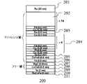
- FIG. 2 is a schematic diagram of a stacked structure of perpendicular magnetization elements (hereinafter referred to as p-MTJ elements) described in Non-Patent Document 2.
- p-MTJ elements perpendicular magnetization elements
- the buffer layer 211 is made of a material containing at least one element of nickel (Ni), iron (Fe), chromium (Cr), and ruthenium (Ru).
- the buffer layer 210 is preferably made of a metal such as tantalum (Ta), hafnium (Hf), niobium (Nb), zirconium (Zr), titanium (Ti), molybdenum (Mo) or tungsten (W), and magnesium.
- CoFeB is deposited as a free layer 209. Further, at least one or two or more alloys of Co and Fe may be disposed between CoFeB and MgO.
- the film thickness of the CoFeB or CoFeB / CoFe magnetic layer is about 0.8 to 2.0 nm in total.
- a barrier layer 208 is formed thereon.
- the barrier layer is preferably MgO in order to obtain a high MR ratio.
- an oxide containing at least one or more of magnesium (Mg), aluminum (Al), titanium (Ti), zinc (Zn), hafnium (Hf), germanium (Ge), and silicon (Si) good.
- the oxide may be formed directly using RF sputtering or the like and oxidized after forming a metal film.
- the oxidation is performed by sealing oxidation of the chamber, flow oxidation while exhausting, radical oxidation using active oxygen, or plasma oxidation.
- a reference layer 207 having a thickness of about 0.2 to 1 nm containing CoFe and the like
- a reference layer 206 having a thickness of about 0.5 to 2.0 nm containing CoFeB and the like and an alignment separation layer 205 containing Ta and the like.
- the reference 2 layer shows a Co / Pd laminated structure as an example, but in addition, a laminated structure such as Co / Pd, Co / Pt, and Co / Ni, an amorphous material such as TbTeCo and GdFeCo, Any form of ordered alloys such as FePt, CoPt, MnGa, and MnAl may be used.
- the reference layer 207 may be omitted and the CoFeB of the reference layer 206 may be in direct contact with the barrier layer 208.
- the alignment separation layer 205 is not limited to tantalum (Ta), hafnium (Hf), niobium (Nb), zirconium (Zr), titanium (Ti), molybdenum (Mo), tungsten (W), platinum (Pt ), At least one or two or more alloys of ruthenium (Ru), magnesium (Mg), aluminum (Al), tantalum (Ta), titanium (Ti), zinc (Zn), hafnium (Hf), germanium (Ge) ), Or an oxide containing at least one or more of silicon (Si).
- a nonmagnetic material having a thickness of about 0.8 nm containing at least one or two or more alloys of ruthenium (Ru), chromium (Cr), rhodium (Rh), iridium (Ir) and rhenium (Re).
- the intermediate layer 203 is formed. On top of that, it is composed of laminated structures such as Co / Pd, Co / Pd, Co / Pt, Co / Ni, amorphous materials such as TbTeCo and GdFeCo, and ordered alloys such as FePt, CoPt, MnGa and MnAl.
- the reference layer 202 is formed.
- a synthetic reference layer is formed by the reference layer 207, the reference layer 206, the alignment separation layer 205, and the stacked structure portion of the reference layer 204, the nonmagnetic intermediate layer 203 and the reference layer 202.
- the reference layer may be formed by the reference layer 207, the reference layer 206, the orientation separation layer 205, and the reference layer 204 without the nonmagnetic intermediate layer 203 and the reference layer 202.
- Ta 5 nm
- Ta may be replaced with a material such as ruthenium (Ru), titanium (Ti), or platinum (Pt).
- Ru ruthenium
- Ti titanium
- Pt platinum
- the buffer layer 211 is 5 nm RuCoFe
- the buffer layer 210 is 2 nm Ta
- the free layer 209 is 0.8 nm CoFeB
- the barrier layer 208 is 0.9 nm MgO.
- the reference layer 207 is 0.5 nm Fe
- the reference layer 206 is 0.8 nm CoFeB
- the orientation separation layer 205 is 0.3 nm Ta
- the reference layer 204 is 0.25 nm Co and 0.8 nm.
- the nonmagnetic intermediate layer 203 is 0.9 nm Ru
- the reference layer 202 is a 14 nm stack of Co and 0.8 nm Pt.
- the cap layer 201 is made of 20 nm Ru.
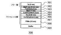
- FIG. 3 is a schematic diagram of a laminated structure of in-plane magnetization type elements (hereinafter referred to as MTJ elements) described in Non-Patent Document 3.
- MTJ elements in-plane magnetization type elements
- the upper Ta serves as a base film, and other than Ta, it can be used as a metal such as hafnium (Hf), niobium (Nb), zirconium (Zr), titanium (Ti), molybdenum (Mo) or tungsten (W). good.
- a layer containing at least one element such as nickel (Ni), iron (Fe), chromium (Cr), ruthenium (Ru), or the like may be formed thereon.
- an antiferromagnetic layer 308 containing, for example, IrMn, PtMn, FeMn, NiMn, RuRhMn, CrPtMn or the like is formed to a thickness of about 3 to 20 nm.
- a reference layer 307 having a thickness of about 1 to 5 nm containing CoFe and the like, and at least one of ruthenium (Ru), chromium (Cr), rhodium (Rh), iridium (Ir), and rhenium (Re)
- a nonmagnetic intermediate layer 306 having a thickness of about 0.8 nm including two or more alloys and a reference layer 305 having a thickness of about 1 to 5 nm including, for example, CoFe, CoFeB, and the like are formed.
- the antiferromagnetic layer 308, the pinned magnetic layer 307, the nonmagnetic intermediate layer 306, and the pinned magnetic layer 305 form a synthetic reference layer.
- the reference layer may have a two-layer structure of an antiferromagnetic layer and a reference two layer.
- the reference layer is a layer whose magnetization direction is fixed.
- a barrier layer 304 is formed thereon.
- the barrier layer 304 is preferably MgO in order to obtain a high MR ratio.
- an oxide containing at least one or more of magnesium (Mg), aluminum (Al), titanium (Ti), zinc (Zn), hafnium (Hf), germanium (Ge), and silicon (Si) good.
- the oxide may be formed directly using RF sputtering or the like and oxidized after forming a metal film. The oxidation is performed by sealing oxidation of the chamber, flow oxidation while exhausting, radical oxidation using active oxygen, or plasma oxidation.
- a free layer 303 having a structure in which one or two or more materials including at least one or two or more alloys such as CoFeB or Co, Fe, Ni, etc. are formed is formed to a thickness of about 1 to 10 nm.
- the free layer 303 is a layer whose magnetization is not fixed, and its electric resistance changes depending on the relative angle to the magnetization of the reference layer.
- An oxide cap layer 302 is formed thereon. This layer has the effect of imparting perpendicular magnetic anisotropy to the magnetization of the free layer, facilitating magnetization reversal by spin torque, and reducing the critical current density Jc0 for magnetization reversal.
- the oxide cap layer contains at least one or more of magnesium (Mg), aluminum (Al), titanium (Ti), zinc (Zn), hafnium (Hf), germanium (Ge), and silicon (Si).
- An oxide or the like can be applied.
- the oxidation is performed by sealing oxidation of the chamber, flow oxidation while exhausting, radical oxidation using active oxygen, or plasma oxidation.
- Ta (5 nm) is formed as a cap layer 301. Ta may be replaced with a material such as ruthenium (Ru), titanium (Ti), or platinum (Pt).
- ruthenium (Ru), titanium (Ti), or platinum (Pt) Such a TMR element is manufactured in a consistent vacuum by a cluster
- the antiferromagnetic layer 308 is 15 nm of PtMn
- the reference layer 307 is 2.5 nm of Co 70 Fe 30
- the nonmagnetic intermediate layer 306 is 0.85 nm of Ru
- the reference layer 305 Is 3 nm Co 60 Fe 20 B 20
- the barrier layer 304 is 1 nm MgO
- the free layer 303 is 2 nm Fe 80 B 20
- the oxide cap layer 302 is 0 to 2.4 nm MgO cap.
- the cap layer 301 is 5 nm of Ta.
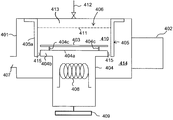
- FIG. 4 is a schematic diagram showing a configuration of the oxidation processing apparatus 400 according to the present embodiment, and is a diagram in a substrate transfer state and a first oxidation process (first oxidation process state).
- FIG. 5 is a schematic diagram illustrating the configuration of the oxidation treatment apparatus 400 according to the present embodiment, and is a diagram illustrating another example of the first oxidation treatment.
- FIG. 6 is a schematic diagram showing the configuration of the oxidation processing apparatus 400 according to the present embodiment, and is a diagram in a second oxidation process (second oxidation process state).
- the barrier layer of each element shown in FIGS. 1 to 3 as an example is formed by the oxidation processing apparatus 400.
- the barrier layer is MgO
- the substrate on which Mg is formed is oxidized in the oxidation processing apparatus 400 to form MgO.
- the “first oxidation treatment” is an oxidation for forming a tunnel barrier layer performed at a temperature at which Mg does not sublime (for example, room temperature).
- the “second oxidation treatment” is an oxidation for forming a tunnel barrier layer that is performed while the substrate is intentionally heated or heated to a predetermined temperature.
- the second oxidation treatment is performed after the first oxidation treatment.
- the temperature at which sublimation does not occur refers to a temperature at which the metal film exceeds the saturated vapor pressure and does not desorb in the vacuum.
- an oxidation processing apparatus 400 includes a processing container 401, a vacuum pump 402 as an exhaust unit for exhausting the inside of the processing container, and a substrate for holding a substrate 403 provided in the processing container 401.
- a holder 404, a cylindrical member 405 provided in the processing container 401, a gas introduction unit 406 as oxygen gas introduction means for introducing oxygen gas into the processing container 401, and a substrate transfer port 407 are provided.
- the substrate transport port 407 is provided with a slit valve.
- the substrate holder 404 projects a substrate holding surface 404a for holding the substrate 403, a mounting portion 404b on which the substrate holding surface 404a is formed, and protrudes from the substrate holding surface 404a to the gas introduction unit 406 side. And a projection (support) 404c that can be supported apart from the substrate holding surface 404a.
- the protruding portion 404c is configured to be able to execute a protruding state in which the protruding portion 404c protrudes from the substrate holding surface 404a and a storage state in which the protruding portion 404c is stored inside the substrate holding surface 404a. Therefore, the substrate 403 is held on the protrusion 404c in the protruding state (FIGS. 4 and 5), and is held on the substrate holding surface 404a in the stored state (FIG. 6).
- a heater 408 as a heating device is provided inside the substrate holder 404.
- the substrate holder 404 is connected to a substrate holder driving unit 409 as position changing means for changing the relative position between the substrate holder 404 and the cylindrical member 405.
- the substrate holder driving unit 409 moves the substrate holder 404 in an arrow direction P (a direction in which the substrate holder 404 is brought closer to the oxidation treatment space 410 and a direction in which the substrate holder 404 is moved away from the oxidation treatment space 410).
- the substrate holder driving unit 409 is also configured to switch the protruding portion 404c between a protruding state and a stored state. That is, under the control of the substrate holder driving unit 409, when the protruding state is established, if the protruding portion 404c is stored in the substrate holder 404, the protruding portion 404c is protruded from the substrate holding surface 404a to establish the stored state.
- the protrusion 404c protruding from the substrate holding surface 404a is stored in the substrate holder 404.
- the substrate holder 404 is moved to the position shown in FIG. 4 by the control of the substrate holder driving unit 409, and the protrusion 404c is moved from the substrate holding surface 404a. Protrude to project.
- the substrate 403 is carried into the processing container 401 through the substrate carrying port 407, and the substrate 403 is placed on the protruding portion 404c.
- the substrate 403 held on the protrusion 404c is unloaded from the processing container 401 through the substrate transfer port 407.
- the first oxidation treatment in the state shown in FIGS. 4 and 5, oxygen gas is introduced into the treatment container 401 by the gas introduction unit 406, whereby Mg is oxidized prior to oxidation while heating. .
- the projection 404c is housed inside the substrate holder 404 under the control of the substrate holder driving unit 409, whereby the substrate 403 is disposed on the substrate holding surface 404a. An oxidation process is performed while heating the substrate 403 (FIG. 6).
- the gas introduction part 406 is provided apart from the wall 401a of the processing container 401 facing the substrate holder 404, and is provided in the shower plate 411 having a large number of holes and the wall 401a, and oxygen gas is introduced into the processing container 401. It has an oxygen introduction path 412 having a gas introduction port for introduction, and a diffusion space 413 for diffusing oxygen gas introduced from the oxygen introduction path 412 between the shower plate 411 and the wall 401a.
- an oxygen introduction path 412 is provided so that oxygen gas is introduced into the diffusion space 413, and the oxygen gas introduced from the oxygen introduction path 412 and diffused in the diffusion space 413 passes through the shower plate 411. Through the substrate. Note that a plurality of oxygen introduction paths 412 may be provided.
- the cylindrical member 405 is attached to the wall 401a so as to surround the region 401b and the shower plate 411 including at least a portion of the wall 401a of the processing vessel 401 to which the oxygen introduction path 412 is connected. It is a member having an extending portion 405a extending toward the opposite side (here, the substrate holder 404 side).
- the cylindrical member 405 is a cylindrical member having a circular cross section cut perpendicularly to the extending direction, but the cross section may have another shape such as a polygon.
- the cylindrical member 405 is made of, for example, aluminum. It is preferable to use aluminum because the cylindrical member 405 can be easily processed.
- titanium or stainless steel (SUS) may be used.
- a shower plate 411 is provided in a space surrounded by the extending portion 405a, that is, in a hollow portion of the tubular member 405, and the portion of the tubular member 405 closer to the wall 401a than the shower plate 411 and the above-described wall 401a
- a diffusion space 413 is formed by at least a part of the region 401 b and the shower plate 411.
- the shower plate 411 and the cylindrical member 405 when the oxygen introduction path 412 and the vacuum pump 402 as the exhaust section do not exist on the same axis (for example, as shown in FIGS. 4 to 5, the oxygen introduction path 412 Even if the oxygen introduction direction of the vacuum pump 402 and the exhaust direction of the vacuum pump 402 are perpendicular to each other, oxygen gas can be supplied uniformly to the surface of the substrate 403 at the position of FIGS. Further, it is possible to reduce the unevenness of the oxidation distribution in the plane of the substrate 403 of MgO caused by oxidation. Therefore, the RA distribution can be improved.
- the shower plate 411 Since oxygen gas is introduced into the oxidation treatment space 410 from the hole of the shower plate 411, the shower plate 411 is provided with a portion of the gas introduction part 406 for introducing oxygen gas into the oxidation treatment space in a limited manner. It can be said that this region is also referred to as an “oxygen gas introduction region”. As an example, when the shower plate 411 is not provided, oxygen gas is limitedly introduced into the oxidation treatment space 410 from the oxygen introduction path 412, so that the region 401b becomes an oxygen gas introduction region. In this embodiment, it can be said that the oxidation treatment space 410 is formed by the oxygen gas introduction region, the cylindrical member 405, and the substrate holder 404 (substrate holding surface 404a).
- the cylindrical member 405 when the substrate holder 404 is inserted into the opening 405 b of the cylindrical member 405, the cylindrical member 405 has at least a part (mounting portion) of the extending portion 405 a and the substrate holder 404.
- a gap 415 is formed between the portion 4b). That is, when the oxidation treatment space 410 is formed, the cylindrical member 405 surrounds the substrate holding surface 404a, and a gap 415 is provided between the mounting portion 404b on which the substrate holding surface 404a is formed and the extending portion 405a. It is configured as follows.
- the oxygen gas introduced into the oxidation treatment space 410 from the gas introduction unit 406 is exhausted from the oxidation treatment space 410 to the external space 414 of the oxidation treatment space 410 through the gap 415.
- the oxygen gas exhausted from the oxidation processing space 410 to the external space 414 through the gap 415 is exhausted from the processing container 401 by the vacuum pump 402.
- the substrate holder driving unit 409 moves the substrate holder 404 in the arrow direction P so that the substrate holding surface 404a is accommodated in the cylindrical member 405, and the substrate holding surface 404a (mounting portion 404b) is inserted into the opening 405b.
- the movement of the substrate holder 404 is stopped at the predetermined position.
- an oxidation treatment space 410 communicating with the external space 414 only by the gap 415 is formed.
- the oxidation treatment space 410 is formed by the shower plate 411, the extending portion 405a, and the substrate holder 404 (substrate holding surface 404a).
- the enclosure for forming the space smaller than the space defined by the inner wall of the processing container 401 with the substrate holding surface 404a inside the processing container 401 is the shower plate 411 and the extension. It is the existing part 405a. Therefore, the cylindrical member 405 showers the oxidation treatment space 410 so that the oxygen gas introduced by the gas introduction unit 406 is introduced into the oxidation treatment space 410 in the treatment vessel 401 only during the oxidation treatment. It is a surrounding member for partitioning together with the plate 411 and the substrate holder 404 (substrate holding surface 404a).
- the oxidation treatment space 410 is formed by the region 401b, the extending portion 405a, and the substrate holder 404. These are a region 401b that is a part of the inner wall of the processing container 401, and an extending portion 405a.
- the substrate holder driving unit 409 may be configured such that the substrate holding surface 404a is rotatable in the in-plane direction of the substrate holding surface 404a. That is, the substrate holder 404 may be configured such that the substrate holding surface 404a rotates about the normal direction of the substrate holding surface 404a.
- an electrostatic chuck ESC
- the substrate 403 may be electrostatically attracted to the substrate holding surface 404a.
- the oxygen pressure on the surface of the substrate 403 it is preferable to make the oxygen pressure on the surface of the substrate 403 uniform. Therefore, even when the gas introduction from the shower plate 411 is not uniform, the gas concentration distribution of the oxygen gas supplied to the surface of the substrate 403 is changed by rotating the substrate 403 by rotating the substrate holding surface 404a. It can be made uniform. Therefore, the RA distribution can be improved.
- the substrate holder driving unit 409 is configured to move the substrate holder 404 along the extending direction of the extending portion 405a inside the cylindrical member 405. That is, the substrate holder driving unit 409 can move the substrate holder 404 in the direction of approaching the shower plate 411 as the oxygen gas introduction region and the direction of moving away from the shower plate 411 inside the cylindrical member 405.
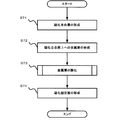
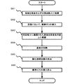
- FIG. 7 is a flowchart showing the procedure of the method of manufacturing the magnetoresistive element according to this embodiment.
- the magnetoresistive element described here has, for example, a structure in which a magnetization free layer, a tunnel barrier layer, and a magnetization fixed layer are stacked in this order on a substrate.
- the present invention may be applied to the manufacture of a magnetoresistive element having a structure in which a magnetization fixed layer, a tunnel barrier layer, and a magnetization free layer are laminated in this order on a substrate.
- a substrate in which a predetermined layer serving as a base layer of a magnetization free layer is formed on a substrate 403 is prepared.
- a magnetization free layer is formed on the underlayer in a film forming chamber.
- a magnetization fixed layer is formed on the base layer. That is, in step S71, one of the magnetization free layer and the magnetization fixed layer is formed on the base layer.
- Mg is formed on the magnetization free layer formed in step S71 in the above-described film formation chamber or another chamber. In this way, the metal film for forming the tunnel barrier layer which is an oxide is formed by this step as the film forming process.
- step S ⁇ b> 73 the substrate 403 on which Mg is formed in step S ⁇ b> 72 is transferred into the oxidation processing apparatus 400 through the substrate transfer port 407, and oxidation processing is performed in the oxidation processing apparatus 400. Details of this oxidation step will be described later.
- step S74 the substrate 403 having MgO (tunnel barrier layer) formed by the oxidation treatment in step S73 is transferred to the above-described film formation chamber or another film formation chamber, and used as a tunnel barrier layer. A magnetization fixed layer is formed on MgO.
- MgO tunnel barrier layer
- a magnetization free layer is formed on MgO. That is, in step S74, the other of the magnetization free layer and the magnetization fixed layer is formed on the tunnel barrier layer.
- FIG. 8 is a flowchart showing the procedure of the oxidation treatment in the tunnel barrier layer forming step according to the present embodiment.
- FIG. 9 is a time chart of the oxidation treatment of FIG.
- the substrate holder 404 has an ESC function and a substrate rotation mechanism.
- step S81 at timing t1, the slit valve of the substrate transfer port 407 is opened to transfer the Mg-formed substrate 403 into the processing container 401, and the substrate 403 is placed on the protruding projection 404c. In this way, the substrate 403 on which Mg is formed is held on the substrate holder.
- the slit valve is closed.
- oxygen gas is introduced into the processing apparatus 401 by the gas introduction unit 406 at the timing t ⁇ b> 3.
- the heater 408 is not driven, and the inside of the processing container 401 is at room temperature.
- Mg on the substrate 403 is oxidized (first oxidation treatment is performed).
- the substrate temperature during the first oxidation treatment is not limited to room temperature, and the substrate 403 may be heated by the heater 408 or an external heating device (not shown) as long as Mg does not sublime.
- the heater 408 may be always driven and the substrate holder 404 may be constantly heated. Also in this case, since the substrate 403 is placed on the protrusion 404c in step S81, the temperature of the substrate 403 is maintained at a temperature at which Mg does not sublime.
- step S83 while maintaining the introduction of the oxygen gas started in step S82, the projection 404c is lowered and stored in the substrate holder 404 at timing t4, whereby on the projection 404c (on the support).
- the substrate 403 placed on the substrate is placed on the substrate holding surface 404a.
- step S84 heating of the substrate 403 placed on the substrate holding surface is started by driving the heater 408 at timing t5 while maintaining the introduction of the oxygen gas started in step S82. That is, the substrate holding surface 404a is heated by the heater 408, and the substrate 403 is heated by the heating. Further, the ESC function of the substrate holder 404 is turned on, and the substrate 403 is electrostatically attracted to the substrate holding surface 404a.
- the substrate 403 can be heated to a desired temperature in a short time, and the substrate 403 reaches a target heating temperature at timing t6.
- oxidation of the Mg formed on the substrate 403 and not oxidized in the first oxidation treatment while being heated (second oxidation treatment) is started.
- the target heating temperature may be equal to or higher than the temperature at which Mg sublimes, or may be lower than that temperature. However, in the heating step, it is preferable to heat the substrate 403 under conditions where Mg does not sublime.
- step S85 while maintaining the introduction of the oxygen gas started in step S82, the substrate holder driving unit 409 is driven at timing t7, so that the substrate holder 404 is formed with the oxidation treatment space 410 as shown in FIG.
- the substrate holder 404 is moved to the position where it will be.
- an oxidation treatment space 410 that is smaller than the treatment vessel 401 is formed inside the treatment vessel 401.
- the substrate holder drive unit 409 is driven to rotate the substrate 403 by rotating the substrate holding surface 404a around the normal direction of the substrate holding surface 404a.
- the substrate 403 may be heated and oxygen introduced while the substrate holder 404 is brought close to the shower plate 411 serving as an oxygen gas introduction region (oxygen gas introduction portion).
- the oxidation treatment space 410 is formed after step S84, but the formation timing of the oxidation treatment space 410 is not limited to this. For example, any timing before step S84 (for example, between step S81 and step S82) may be used.
- step S86 the gas introduction unit 406 is controlled at timing t8, and the oxygen introduction started in step S82 is stopped.
- the substrate holder driving unit 409 is controlled so that the substrate holding surface 404a is stopped and the substrate holder 404 is moved to the position shown in FIG.
- the driving of the heater 408 is stopped at timing t9, the ESC function is turned off, and the protruding portion 404c in the housed state is raised and protruded from the substrate holding surface 404a at timing t10, and the substrate 403 on which MgO is formed protrudes. Held on the portion 404c.
- the slit valve of the substrate transfer port 407 is opened at timing t11, the substrate held on the projection 404c is carried out of the processing container 401, and the slit valve is closed at timing t12.
- the vacuum pump 402 connected to the processing container 401 is always driven, and the inside of the processing container 401 is always evacuated in steps S81 to S86 described above.
- the present invention is not limited to this, and the vacuum pump 402 may be driven in a limited manner in accordance with each step.
- the oxygen gas is supplied in a state where the substrate 403 is held away from the substrate holding surface 404a by the protrusions 404c, and Mg formed on the substrate 403 at room temperature, which is a temperature at which Mg does not sublime. Is first oxidized. Accordingly, the Mg surface (exposed surface) on the substrate 403 and its vicinity can be oxidized at a temperature at which Mg does not sublime.
- the magnesium (Mg) film has a lower vapor pressure than other metal films. For example, as can be seen from FIG. 10, in an atmosphere of 1 ⁇ 10 ⁇ 9 to 1 ⁇ 10 ⁇ 8 Torr, sublimation of Mg starts at about 423 K (about 150 ° C.).
- Mg formed on the substrate 403 is sublimated at a temperature of about 150 ° C. or higher in an atmosphere of 1 ⁇ 10 ⁇ 9 to 1 ⁇ 10 ⁇ 8 Torr, and the Mg is vaporized.
- the oxygen oxidation treatment is performed by supplying oxygen gas at a temperature at which Mg does not sublime.
- the protrusion 404c is accommodated in the substrate holder 404 and held on the protrusion 404c, and the substrate 403 on which the surface and its vicinity are converted to MgO is formed on the substrate holding surface 404a.
- the substrate 403 placed on the substrate holding surface 404a is heated to a predetermined temperature by the heater 408, and an oxidation process (second oxidation process) is performed at a low pressure. Therefore, Mg that has not been oxidized by the first oxidation treatment is oxidized with a strong oxidizing power by the oxidation while heating.
- oxidation with heating has a problem that the amount of Mg sublimation increases, particularly in a high vacuum.
- the surface of Mg formed on the substrate 403 by the first oxidation treatment and its vicinity are converted to MgO before the oxidation with heating. Therefore, since MgO formed by the first oxidation treatment hardly undergoes sublimation, it functions as a cap layer that suppresses sublimation for the lower layer Mg (the surface of Mg and the inner region from the vicinity thereof).
- the oxygen gas is introduced from the stage before heating the substrate 403 to perform the oxidation process (first oxidation process), the oxidation process (second oxidation) while heating the substrate is performed.
- first oxidation process the oxidation process
- second oxidation the oxidation process while heating the substrate is performed.
- the substrate holding surface 404a for heating the substrate 403 is heated after the substrate 403 is placed on the substrate holding surface 404a (after step S83).
- the heating of 404a may be performed before step S83. For example, it may be performed between step S81 and step S83.
- the substrate holding surface 404a is in a necessary heating state when the substrate 403 is placed on the substrate holding surface 404a for the second oxidation treatment. Therefore, the waiting time until the substrate holding surface 404a is heated to a desired temperature can be shortened, and the throughput can be further improved.
- the substrate is heated in step S84 after the introduction of oxygen in step S82.
- what is important in this embodiment is to form MgO formed while reducing sublimation of Mg as much as possible on the surface of Mg and in the vicinity thereof before oxidation while heating the substrate. Therefore, if this can be realized, oxygen gas introduction and substrate heating may be performed simultaneously.
- the substrate 403 may be placed on the substrate holding surface 404a without providing the protrusions 404c, and oxygen introduction by the gas introduction unit 406 and substrate heating by the heater 408 may be performed simultaneously.
- the substrate temperature is a temperature at which Mg does not sublime during a predetermined period from the substrate heating. It can be said that the sublimation is suppressed as much as possible (first oxidation treatment). As the substrate temperature rises, the process continuously changes from the first oxidation process to the second oxidation process.
- the second oxidation treatment is an oxidation treatment for uniformly oxidizing in the Mg plane, and is an oxidation treatment while heating the substrate temperature to a predetermined temperature or higher. is there.
- the first oxidation treatment is an oxidation treatment for forming MgO that functions as a cap layer with respect to the sublimation of Mg due to the oxidation in the second oxidation treatment and reducing the sublimation of Mg.
- this is an oxidation treatment performed by supplying oxygen to the substrate 403 at a substrate temperature at which Mg does not sublime (for example, room temperature).
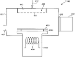
- FIG. 11 is a schematic diagram showing a schematic configuration of the oxidation treatment apparatus according to the present embodiment.
- the oxidation processing apparatus 1100 has the same structure as the oxidation processing apparatus 400 shown in FIGS. 4 to 6 except that the cylindrical member 405 is not provided.
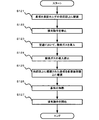
- FIG. 12 is a flowchart showing the procedure of the oxidation treatment in the tunnel barrier layer forming step according to the present embodiment.
- step S121 the slit valve of the substrate transfer port 407 is opened to transfer the Mg-formed substrate 403 into the processing container 401, and the substrate 403 is placed on the protruding portion 404c.
- the slit valve is closed.
- step S122 the gate valve 416 that has been opened is closed to stop the exhaust operation. If the vacuum pump 402 is not driven in step S121, this step is unnecessary.
- step S ⁇ b> 123 oxygen gas is introduced into the processing apparatus 401 by the gas introduction unit 406. At this time, the heater 408 is not driven, and the inside of the processing container 401 is at room temperature. By this oxygen introduction, Mg on the substrate 403 is oxidized (first oxidation treatment is performed).
- step S124 the oxygen introduction started in step S123 is stopped. Even if the introduction of oxygen gas is stopped by this step, the processing container 401 is filled with a predetermined amount of oxygen gas, and an oxygen atmosphere is formed.
- step S125 in a state where the introduction of oxygen gas is stopped, the projection 404c is lowered and stored in the substrate holder 404, whereby the substrate 403 disposed on the projection 404c is placed on the substrate holding surface 404a. Place.
- step S126 with the introduction of oxygen gas stopped, the heater 408 is driven to start heating the substrate 403 placed on the substrate holding surface 404a. That is, the substrate holding surface 404a is heated by the heater 408, and the substrate 403 is heated by the heating.
- step S124 the introduction of oxygen gas is stopped, but since an oxygen atmosphere is formed around the substrate 403, the first of the Mg formed on the substrate 403 by the heating in this heating step.
- the oxidation (second oxidation treatment) of Mg that has not been oxidized by the oxidation treatment while being heated is started.
- step S127 the gate valve 416 closed in step S122 is opened to start the exhaust operation. If the vacuum pump 402 is not driven in step S121, the driving of the vacuum pump 402 is restarted in step S1272 and the inside of the processing container 401 is exhausted.
- an oxygen gas resupply step of supplying the oxygen gas again into the processing container 401 by the gas introduction unit 406 may be performed between step S125 and step S126.
- a process for stopping the supply of oxygen gas may be performed after step S126.
- the substrate 403 is heated while supplying the oxygen gas reintroduced in the oxygen gas resupply process.
Landscapes
- Engineering & Computer Science (AREA)
- Manufacturing & Machinery (AREA)
- Hall/Mr Elements (AREA)
- Mram Or Spin Memory Techniques (AREA)
- Formation Of Insulating Films (AREA)
Abstract
Description
図4は、本実施形態に係る酸化処理装置400の構成を示す模式図であって、基板搬送状態、および第1の酸化処理(第1の酸化プロセス状態)における図である。図5は、本実施形態に係る酸化処理装置400の構成を示す模式図であって、第1の酸化処理の他の例を示す図である。図6は、本実施形態に係る酸化処理装置400の構成を示す模式図であって、第2の酸化処理(第2の酸化プロセス状態)における図である。本実施形態では、酸化処理装置400により、例として挙げた図1~図3に示す各素子のバリア層を形成する。本実施形態では、バリア層はMgOであり、Mgが形成された基板を酸化処理装置400内において酸化処理してMgOを形成する。
なお、本実施形態において、「第1の酸化処理」とは、Mgが昇華しない温度(例えば、室温)で行うトンネルバリア層形成のための酸化である。また、「第2の酸化処理」とは、基板を意図的に加熱しながら、もしくは所定の温度に加熱された状態で行うトンネルバリア層形成のための酸化である。本実施形態では、第1の酸化処理の後に第2の酸化処理を行う。ここで、本発明において、昇華しない温度とは、飽和蒸気圧を超えて金属膜が真空中に脱離しない温度を指す。
なお、一例としてシャワープレート411を設けない場合は、酸素ガスは、酸素導入経路412から酸化処理空間410内に限定的に導入されるので、領域401bが酸素ガス導入領域となる。
本実施形態では、酸素ガス導入領域、筒部材405、および基板ホルダ404(基板保持面404a)により、酸化処理空間410が形成されると言える。
なお、上述のように一例としてシャワープレート411を設けない場合は、酸化処理空間410は、領域401bと、延在部405aと、基板ホルダ404とにより形成されるので、この場合は、上記囲み部は、処理容器401の内壁の一部である領域401b、および延在部405aである。
酸素分布を良くし、RA分布を良くするためには、基板403表面における酸素圧力を均一にすることが好ましい。従って、シャワープレート411からのガス導入が不均一であった場合でも、基板保持面404aが回転することで基板403を回転させることにより、基板403の表面に供給される酸素ガスのガス濃度分布を均一にすることができる。よって、RA分布を向上することができる。
まず、基板403上に磁化自由層の下地層となる所定の層を形成したものを用意する。ステップS71では、ある成膜チャンバにおいて、上記下地層上に磁化自由層を形成する。他の例として、磁化固定層、トンネルバリア層、磁化自由層を順に積層させた構造の場合は、上記下地層上に磁化固定層を形成する。すなわち、ステップS71では、上記下地層上に、磁化自由層および磁化固定層の一方を形成する。
ステップS72では、上記ある成膜チャンバ、または他のチャンバにおいて、ステップS71にて成膜された磁化自由層上にMgを形成する。このように成膜工程としての本ステップにより、酸化物であるトンネルバリア層を形成するための前記金属膜を成膜する。
ステップS74では、ステップS73にて酸化処理が施されて形成されたMgO(トンネルバリア層)を有する基板403を、上記ある成膜チャンバ、または他の成膜チャンバに搬送し、トンネルバリア層としてのMgO上に磁化固定層を形成する。上記他の例として、磁化固定層、トンネルバリア層、磁化自由層を順に積層させた構造の場合は、MgO上に磁化自由層を形成する。すなわち、ステップS74では、トンネルバリア層上に、磁化自由層および磁化固定層の他方を形成する。
ステップS81では、タイミングt1において基板搬送口407のスリットバルブを開けてMgが形成された基板403を処理容器401内に搬送し、突出状態の突起部404c上に基板403を載置する。このようにして基板ホルダ上にMgが形成された基板403が保持される。タイミングt2において、上記スリットバルブを閉じる。
ステップS84では、ステップS82にて開始された酸素ガスの導入を維持しながら、タイミングt5においてヒータ408を駆動して基板保持面上に載置された基板403の加熱を開始する。すなわち、ヒータ408により基板保持面404aを加熱し、該加熱により基板403を加熱する。また、基板ホルダ404のESC機能をオンし、基板403を基板保持面404aに静電吸着させる。このESC機能オンにより、基板403を短時間で所望の温度に加熱することができ、タイミングt6において、基板403は目標の加熱温度となる。本ステップにより、基板403に形成され、第1の酸化処理にて酸化されていないMgの、加熱されながらの酸化(第2の酸化処理)が開始される。上記目標の加熱温度は、Mgが昇華する温度以上であっても良いし、その温度未満であっても良い。ただし、該加熱工程では、Mgが昇華しない条件において基板403を加熱することが好ましい。
なお、本実施形態では、ステップS84の後に酸化処理空間410を形成しているが、該酸化処理空間410の形成のタイミングはこれに限定されない。例えば、ステップS84の前のいずれのタイミング(例えば、ステップS81とステップS82との間など)であっても良い。
第1の実施形態では、処理容器401内に、該処理容器401よりも小さい酸化処理空間410を形成しているが、該酸化処理空間410を形成しなくても良い。図11は、本実施形態に係る酸化処理装置の概略構成を示す模式図である。酸化処理装置1100は、筒部材405を備えていない点を除いては図4~6に示す酸化処理装置400と同一の構造である。
ステップS121では、基板搬送口407のスリットバルブを開けてMgが形成された基板403を処理容器401内に搬送し、突出状態の突起部404c上に基板403を載置する。上記基板載置が終了すると、上記スリットバルブを閉じる。
ステップS125では、酸素ガスの導入が停止された状態で、突起部404cが下降して基板ホルダ404内に収納され、これにより、突起部404c上に配置された基板403を基板保持面404a上に載置する。
Claims (26)
- 磁化自由層および磁化固定層の一方を形成する工程と、
前記形成された磁化自由層および磁化固定層の一方の上にトンネルバリア層を形成する工程と、
前記トンネルバリア層上に前記磁化自由層および前記磁化固定層の他方を形成する工程とを有する磁気抵抗効果素子の製造方法であって、
前記トンネルバリア層を形成する工程は、
基板上に金属膜を成膜する成膜工程と、
前記金属膜を酸化処理する酸化工程とを有し、
前記酸化工程は、
前記酸化処理を行う処理容器内の基板ホルダ上に前記金属膜が形成された基板を保持させる工程と、
前記処理容器内に前記金属膜が昇華しない温度で酸素ガスを導入し、前記基板に前記酸素ガスを供給する工程と、
前記酸素ガスの導入と同時、または該酸素ガスの導入の後に、前記基板を加熱する加熱工程と
を有することを特徴とする磁気抵抗効果素子の製造方法。 - 前記基板を保持させる工程は、前記基板ホルダの基板保持面から突出させた支持部上に前記基板を載置し、
前記供給する工程は、前記支持部上に前記基板を載置した状態で、前記金属膜が昇華しない温度で酸素ガスを前記基板に供給し、
前記製造方法は、前記支持部に載置された基板を前記基板保持面上に載置する工程をさらに有し、
前記加熱工程は、前記基板保持面上に載置された基板を加熱することを特徴とする請求項1に記載の磁気抵抗効果素子の製造方法。 - 前記載置する工程の前に前記基板保持面を加熱することを特徴とする請求項2に記載の磁気抵抗効果素子の製造方法。
- 前記加熱工程の前に前記酸素ガスの供給を停止する工程をさらに有することを特徴とする請求項2に記載の磁気抵抗効果素子の製造方法。
- 前記停止する工程は、前記載置する工程の前に前記酸素ガスの供給を停止し、
前記載置する工程の後に、前記酸素ガスを前記基板に供給する酸素ガス再供給工程をさらに有することを特徴とする請求項4に記載の磁気抵抗効果素子の製造方法。 - 前記加熱工程は、前記酸素ガス再供給工程にて供給された酸素ガスを供給しながら、前記基板を加熱することを特徴とする請求項5に記載の磁気抵抗効果素子の製造方法。
- 前記酸素ガス再供給工程は、前記処理容器における前記酸素ガスの導入部に前記基板を近づけながら前記酸素ガスの供給を行うことを特徴とする請求項5に記載の磁気抵抗効果素子の製造方法。
- 前記酸素ガス再供給工程は、前記基板を該基板の面内方向に回転させながら前記酸素ガスを供給することを特徴とする請求項5に記載の磁気抵抗効果素子の製造方法。
- 前記載置する工程および前記加熱工程では、前記導入する工程による前記酸素ガスの導入が維持されていることを特徴とする請求項2に記載の磁気抵抗効果素子の製造方法。
- 前記加熱工程は、前記処理容器における前記酸素ガスの導入部に前記基板を近づけながら前記基板を加熱することを特徴とする請求項9に記載の磁気抵抗効果素子の製造方法。
- 前記加熱工程は、前記基板を該基板の面内方向に回転させながら前記基板を加熱することを特徴とする請求項9に記載の磁気抵抗効果素子の製造方法。
- 前記金属膜は、マグネシウムであることを特徴とする請求項1に記載の磁気抵抗効果素子の製造方法。
- 前記加熱工程は、前記金属膜が昇華しない条件において前記基板を加熱することを特徴とする請求項1に記載の磁気抵抗効果素子の製造方法。
- 磁化自由層および磁化固定層の一方を形成する工程と、
前記形成された磁化自由層および磁化固定層の一方の上にトンネルバリア層を形成する工程と、
前記トンネルバリア層上に前記磁化自由層および前記磁化固定層の他方を形成する工程とを有する磁気抵抗効果素子の製造方法であって、
前記トンネルバリア層を形成する工程は、
基板上に金属膜を成膜する成膜工程と、
前記金属膜を酸化処理する酸化工程とを有し、
前記酸化工程は、
前記酸化処理を行う処理容器内の基板ホルダ上に前記金属膜が形成された基板を保持させる工程と、
前記処理容器内に前記金属膜が昇華しない温度で酸素ガスを導入し、前記基板に前記酸素ガスを供給する工程と、
前記酸素ガスの導入と同時、または該酸素ガスの導入の後に、前記基板を加熱する加熱工程とを有し、
前記酸化工程は、前記保持させる工程の後に、前記基板ホルダの前記処理容器に対する相対位置を変化させて、前記基板ホルダが有する基板保持面と、前記処理容器内に設けられた囲み部とにより形成される空間を、前記処理容器内に形成する工程であって、前記囲み部により前記基板保持面が囲まれ、かつ該囲み部と前記基板ホルダとの間に間隙が形成されるように前記空間を形成する工程をさらに有し、
前記空間内に導入された酸素ガスは、前記間隙を通して該空間から排気されることを特徴とする酸化方法。 - 前記基板を保持させる工程は、前記基板保持面から突出させた支持部上に前記基板を載置し、
前記導入する工程は、前記支持部上に前記基板を載置した状態で、前記金属膜が昇華しない温度で酸素ガスを前記基板に供給し、
前記製造方法は、前記支持部に載置された基板を、前記基板保持面上に載置する工程をさらに有し、
前記加熱工程は、前記基板保持面上に載置された基板を加熱することを特徴とする請求項14に記載の磁気抵抗効果素子の製造方法。 - 前記載置する工程の前に前記基板保持面を加熱することを特徴とする請求項15に記載の磁気抵抗効果素子の製造方法。
- 前記加熱工程の前に前記酸素ガスの供給を停止する工程をさらに有することを特徴とする請求項15に記載の磁気抵抗効果素子の製造方法。
- 前記停止する工程は、前記載置する工程の前に前記酸素ガスの供給を停止し、
前記載置する工程の後に、前記酸素ガスを前記基板に供給する酸素ガス再供給工程をさらに有することを特徴とする請求項17に記載の磁気抵抗効果素子の製造方法。 - 前記加熱工程は、前記酸素ガス再供給工程にて前記酸素ガスを供給しながら、前記基板を加熱することを特徴とする請求項18に記載の磁気抵抗効果素子の製造方法。
- 前記酸素ガス再供給工程は、前記処理容器における前記酸素ガスの導入部に前記基板を近づけながら前記酸素ガスの供給を行うことを特徴とする請求項18に記載の磁気抵抗効果素子の製造方法。
- 前記酸素ガス再供給工程は、前記基板を該基板の面内方向に回転させながら前記酸素ガスを供給することを特徴とする請求項18に記載の磁気抵抗効果素子の製造方法。
- 前記載置する工程および前記加熱工程では、前記導入する工程による前記酸素ガスの導入が維持されていることを特徴とする請求項15に記載の磁気抵抗効果素子の製造方法。
- 前記加熱工程は、前記処理容器における前記酸素ガスの導入部に前記基板を近づけながら前記基板を加熱することを特徴とする請求項22に記載の磁気抵抗効果素子の製造方法。
- 前記加熱工程は、前記基板を該基板の面内方向に回転させながら前記基板を加熱することを特徴とする請求項22に記載の磁気抵抗効果素子の製造方法。
- 前記金属膜は、マグネシウムであることを特徴とする請求項14に記載の磁気抵抗効果素子の製造方法。
- 前記加熱工程は、前記金属膜が昇華しない条件において前記基板を加熱することを特徴とする請求項14に記載の磁気抵抗効果素子の製造方法。
Priority Applications (6)
| Application Number | Priority Date | Filing Date | Title |
|---|---|---|---|
| JP2014552881A JP5882502B2 (ja) | 2012-12-20 | 2013-09-04 | 磁気抵抗効果素子の製造方法 |
| DE112013006168.6T DE112013006168B4 (de) | 2012-12-20 | 2013-09-04 | Verfahren zum Herstellen eines Magnetowiderstandelements |
| CN201380067306.2A CN104885245B (zh) | 2012-12-20 | 2013-09-04 | 磁阻元件的制造方法 |
| KR1020157015986A KR101743498B1 (ko) | 2012-12-20 | 2013-09-04 | 자기저항 효과 소자의 제조 방법 |
| SG11201504875UA SG11201504875UA (en) | 2012-12-20 | 2013-09-04 | Method for manufacturing magnetoresistance effect element |
| US14/742,169 US9865805B2 (en) | 2012-12-20 | 2015-06-17 | Method for manufacturing magnetoresistive element |
Applications Claiming Priority (2)
| Application Number | Priority Date | Filing Date | Title |
|---|---|---|---|
| JP2012-278264 | 2012-12-20 | ||
| JP2012278264 | 2012-12-20 |
Related Child Applications (1)
| Application Number | Title | Priority Date | Filing Date |
|---|---|---|---|
| US14/742,169 Continuation US9865805B2 (en) | 2012-12-20 | 2015-06-17 | Method for manufacturing magnetoresistive element |
Publications (1)
| Publication Number | Publication Date |
|---|---|
| WO2014097510A1 true WO2014097510A1 (ja) | 2014-06-26 |
Family
ID=50977880
Family Applications (1)
| Application Number | Title | Priority Date | Filing Date |
|---|---|---|---|
| PCT/JP2013/005249 Ceased WO2014097510A1 (ja) | 2012-12-20 | 2013-09-04 | 磁気抵抗効果素子の製造方法 |
Country Status (8)
| Country | Link |
|---|---|
| US (1) | US9865805B2 (ja) |
| JP (1) | JP5882502B2 (ja) |
| KR (1) | KR101743498B1 (ja) |
| CN (1) | CN104885245B (ja) |
| DE (1) | DE112013006168B4 (ja) |
| SG (1) | SG11201504875UA (ja) |
| TW (1) | TWI552399B (ja) |
| WO (1) | WO2014097510A1 (ja) |
Cited By (6)
| Publication number | Priority date | Publication date | Assignee | Title |
|---|---|---|---|---|
| JP5848494B1 (ja) * | 2015-02-02 | 2016-01-27 | キヤノンアネルバ株式会社 | 垂直磁化型mtj素子の製造方法 |
| JP2016033244A (ja) * | 2014-07-31 | 2016-03-10 | 東京エレクトロン株式会社 | 成膜装置及び成膜方法 |
| US9502644B1 (en) | 2015-10-21 | 2016-11-22 | Canon Anelva Corporation | Method for manufacturing magnetoresistive device |
| JP2018502450A (ja) * | 2015-01-15 | 2018-01-25 | マイクロン テクノロジー, インク. | 半導体デバイス、磁気トンネル接合およびその製造方法 |
| US10153426B2 (en) | 2013-11-18 | 2018-12-11 | Canon Anelva Corporation | Manufacturing method of magnetoresistive effect element |
| WO2019049244A1 (ja) * | 2017-09-06 | 2019-03-14 | Tdk株式会社 | トンネル磁気抵抗効果素子及び磁気メモリ |
Families Citing this family (11)
| Publication number | Priority date | Publication date | Assignee | Title |
|---|---|---|---|---|
| KR101800237B1 (ko) | 2015-05-22 | 2017-11-22 | 캐논 아네르바 가부시키가이샤 | 자기저항 효과 소자 |
| US10050192B2 (en) * | 2015-12-11 | 2018-08-14 | Imec Vzw | Magnetic memory device having buffer layer |
| CN107264075B (zh) * | 2016-04-08 | 2020-11-06 | 株式会社御牧工程 | 粘接方法、墨层形成体的制造方法及墨层形成体 |
| US10361361B2 (en) | 2016-04-08 | 2019-07-23 | International Business Machines Corporation | Thin reference layer for STT MRAM |
| JP6280610B1 (ja) * | 2016-10-03 | 2018-02-14 | Tdk株式会社 | 磁気抵抗効果素子及びその製造方法、並びに位置検出装置 |
| US10741742B2 (en) | 2018-02-28 | 2020-08-11 | The Regents Of The University Of Colorado, A Body Corporate | Enhanced superconducting transition temperature in electroplated rhenium |
| US11542589B2 (en) * | 2018-03-21 | 2023-01-03 | Applied Materials, Inc. | Resistance-area (RA) control in layers deposited in physical vapor deposition chamber |
| US10648069B2 (en) | 2018-10-16 | 2020-05-12 | Taiwan Semiconductor Manufacturing Company, Ltd. | Monolayer-by-monolayer growth of MgO layers using Mg sublimation and oxidation |
| CN110098318B (zh) * | 2019-05-10 | 2020-11-03 | 北京航空航天大学 | 具有界面垂直磁各向异性的多膜层结构及磁随机存储器 |
| US11177430B2 (en) | 2019-06-17 | 2021-11-16 | Taiwan Semiconductor Manufacturing Co., Ltd. | Memory device and manufacturing method thereof |
| JP7583566B2 (ja) * | 2020-09-23 | 2024-11-14 | 東京エレクトロン株式会社 | 磁気抵抗効果素子の製造方法、酸化処理装置、及び基板処理システム |
Citations (3)
| Publication number | Priority date | Publication date | Assignee | Title |
|---|---|---|---|---|
| WO2010044134A1 (ja) * | 2008-10-14 | 2010-04-22 | キヤノンアネルバ株式会社 | 磁気抵抗効果素子の製造方法及び磁気抵抗効果素子製造プログラム |
| WO2012086183A1 (ja) * | 2010-12-22 | 2012-06-28 | 株式会社アルバック | トンネル磁気抵抗素子の製造方法 |
| JP2013145846A (ja) * | 2012-01-16 | 2013-07-25 | Ulvac Japan Ltd | トンネル磁気抵抗素子の製造方法、及びトンネル磁気抵抗素子の製造装置 |
Family Cites Families (26)
| Publication number | Priority date | Publication date | Assignee | Title |
|---|---|---|---|---|
| KR0165484B1 (ko) | 1995-11-28 | 1999-02-01 | 김광호 | 탄탈륨산화막 증착 형성방법 및 그 장치 |
| JP2000232222A (ja) * | 1999-02-10 | 2000-08-22 | Nec Corp | 半導体装置の製造方法 |
| JP2002043299A (ja) * | 2000-07-19 | 2002-02-08 | Tokyo Electron Ltd | 被処理体の熱処理方法 |
| JP2003304012A (ja) * | 2002-04-10 | 2003-10-24 | Matsushita Electric Ind Co Ltd | トンネル磁気抵抗効果素子 |
| WO2003092084A1 (en) | 2002-04-23 | 2003-11-06 | Matsushita Electric Industrial Co., Ltd. | Magnetoresistive element, manufacturing method thereof, magnetic head, magnetic memory, and magnetic recording device using the same |
| US6774012B1 (en) * | 2002-11-08 | 2004-08-10 | Cypress Semiconductor Corp. | Furnace system and method for selectively oxidizing a sidewall surface of a gate conductor by oxidizing a silicon sidewall in lieu of a refractory metal sidewall |
| EP1843386A1 (en) * | 2005-01-18 | 2007-10-10 | Nikon Corporation | Liquid removing apparatus, exposure apparatus and device manufacturing method |
| US20070116888A1 (en) * | 2005-11-18 | 2007-05-24 | Tokyo Electron Limited | Method and system for performing different deposition processes within a single chamber |
| WO2008011579A2 (en) | 2006-07-21 | 2008-01-24 | Aixtron, Inc. | Small volume symmetric flow single wafer ald apparatus |
| JP5210533B2 (ja) | 2006-09-21 | 2013-06-12 | アルプス電気株式会社 | トンネル型磁気検出素子及びその製造方法 |
| CN100557840C (zh) * | 2006-09-21 | 2009-11-04 | 阿尔卑斯电气株式会社 | CoFeB层构成固定层至少一部分的隧道型磁检测元件及其制法 |
| JP2008103662A (ja) | 2006-09-21 | 2008-05-01 | Alps Electric Co Ltd | トンネル型磁気検出素子及びその製造方法 |
| WO2009031232A1 (ja) * | 2007-09-07 | 2009-03-12 | Canon Anelva Corporation | スパッタリング方法および装置 |
| US20130134032A1 (en) | 2008-06-25 | 2013-05-30 | Canon Anelva Corporation | Method of fabricating and apparatus of fabricating tunnel magnetic resistive element |
| WO2009157064A1 (ja) | 2008-06-25 | 2009-12-30 | キヤノンアネルバ株式会社 | トンネル磁気抵抗素子の製造方法および製造装置 |
| WO2010008021A1 (ja) * | 2008-07-15 | 2010-01-21 | キヤノンアネルバ株式会社 | プラズマ処理方法及びプラズマ処理装置 |
| JP5320171B2 (ja) * | 2009-06-05 | 2013-10-23 | 東京エレクトロン株式会社 | 基板処理装置 |
| GB2483421B (en) * | 2009-06-24 | 2013-10-09 | Canon Anelva Corp | Vacuum heating/cooling apparatus and manufacturing method of magnetoresistance element |
| US8609262B2 (en) * | 2009-07-17 | 2013-12-17 | Magic Technologies, Inc. | Structure and method to fabricate high performance MTJ devices for spin-transfer torque (STT)-RAM application |
| JP5247619B2 (ja) | 2009-07-28 | 2013-07-24 | キヤノンアネルバ株式会社 | 誘電体膜、誘電体膜を用いた半導体装置の製造方法及び半導体製造装置 |
| TW201135845A (en) * | 2009-10-09 | 2011-10-16 | Canon Anelva Corp | Acuum heating and cooling apparatus |
| JP2011134909A (ja) * | 2009-12-24 | 2011-07-07 | Hitachi Kokusai Electric Inc | 半導体装置の製造方法及び基板処理システム |
| CN102687297B (zh) * | 2009-12-28 | 2014-12-24 | 佳能安内华股份有限公司 | 磁阻元件的制造方法 |
| WO2011081202A1 (ja) | 2009-12-29 | 2011-07-07 | キヤノンアネルバ株式会社 | 電子部品の製造方法、電子部品、プラズマ処理装置、制御プログラム及び記録媒体 |
| JP5458177B2 (ja) | 2010-12-28 | 2014-04-02 | キヤノンアネルバ株式会社 | 半導体装置の製造方法および装置 |
| WO2014024358A1 (ja) | 2012-08-10 | 2014-02-13 | キヤノンアネルバ株式会社 | トンネル磁気抵抗素子の製造装置 |
-
2013
- 2013-09-04 SG SG11201504875UA patent/SG11201504875UA/en unknown
- 2013-09-04 CN CN201380067306.2A patent/CN104885245B/zh active Active
- 2013-09-04 KR KR1020157015986A patent/KR101743498B1/ko active Active
- 2013-09-04 JP JP2014552881A patent/JP5882502B2/ja active Active
- 2013-09-04 DE DE112013006168.6T patent/DE112013006168B4/de active Active
- 2013-09-04 WO PCT/JP2013/005249 patent/WO2014097510A1/ja not_active Ceased
- 2013-12-19 TW TW102147233A patent/TWI552399B/zh active
-
2015
- 2015-06-17 US US14/742,169 patent/US9865805B2/en active Active
Patent Citations (3)
| Publication number | Priority date | Publication date | Assignee | Title |
|---|---|---|---|---|
| WO2010044134A1 (ja) * | 2008-10-14 | 2010-04-22 | キヤノンアネルバ株式会社 | 磁気抵抗効果素子の製造方法及び磁気抵抗効果素子製造プログラム |
| WO2012086183A1 (ja) * | 2010-12-22 | 2012-06-28 | 株式会社アルバック | トンネル磁気抵抗素子の製造方法 |
| JP2013145846A (ja) * | 2012-01-16 | 2013-07-25 | Ulvac Japan Ltd | トンネル磁気抵抗素子の製造方法、及びトンネル磁気抵抗素子の製造装置 |
Cited By (13)
| Publication number | Priority date | Publication date | Assignee | Title |
|---|---|---|---|---|
| US10153426B2 (en) | 2013-11-18 | 2018-12-11 | Canon Anelva Corporation | Manufacturing method of magnetoresistive effect element |
| JP2016033244A (ja) * | 2014-07-31 | 2016-03-10 | 東京エレクトロン株式会社 | 成膜装置及び成膜方法 |
| JP2018502450A (ja) * | 2015-01-15 | 2018-01-25 | マイクロン テクノロジー, インク. | 半導体デバイス、磁気トンネル接合およびその製造方法 |
| WO2016125200A1 (ja) * | 2015-02-02 | 2016-08-11 | キヤノンアネルバ株式会社 | 垂直磁化型mtj素子の製造方法 |
| JP5848494B1 (ja) * | 2015-02-02 | 2016-01-27 | キヤノンアネルバ株式会社 | 垂直磁化型mtj素子の製造方法 |
| US9929340B2 (en) | 2015-02-02 | 2018-03-27 | Canon Anelva Corporation | Method of manufacturing perpendicular MTJ device |
| US9502644B1 (en) | 2015-10-21 | 2016-11-22 | Canon Anelva Corporation | Method for manufacturing magnetoresistive device |
| GB2548644A (en) * | 2015-10-21 | 2017-09-27 | Canon Anelva Corp | Production method for magnetoresistive element |
| TWI613846B (zh) * | 2015-10-21 | 2018-02-01 | Canon Anelva Corp | 磁阻元件的製造方法 |
| WO2017068611A1 (ja) * | 2015-10-21 | 2017-04-27 | キヤノンアネルバ株式会社 | 磁気抵抗素子の製造方法 |
| JP6084335B1 (ja) * | 2015-10-21 | 2017-02-22 | キヤノンアネルバ株式会社 | 磁気抵抗素子の製造方法 |
| GB2548644B (en) * | 2015-10-21 | 2020-09-02 | Canon Anelva Corp | Method for manufacturing magnetoresistive device |
| WO2019049244A1 (ja) * | 2017-09-06 | 2019-03-14 | Tdk株式会社 | トンネル磁気抵抗効果素子及び磁気メモリ |
Also Published As
| Publication number | Publication date |
|---|---|
| US20160005958A1 (en) | 2016-01-07 |
| SG11201504875UA (en) | 2015-07-30 |
| TW201448301A (zh) | 2014-12-16 |
| KR20150090125A (ko) | 2015-08-05 |
| TWI552399B (zh) | 2016-10-01 |
| KR101743498B1 (ko) | 2017-06-05 |
| CN104885245B (zh) | 2017-06-13 |
| JPWO2014097510A1 (ja) | 2017-01-12 |
| DE112013006168T5 (de) | 2015-09-17 |
| JP5882502B2 (ja) | 2016-03-09 |
| US9865805B2 (en) | 2018-01-09 |
| CN104885245A (zh) | 2015-09-02 |
| DE112013006168B4 (de) | 2023-12-28 |
Similar Documents
| Publication | Publication Date | Title |
|---|---|---|
| JP5882502B2 (ja) | 磁気抵抗効果素子の製造方法 | |
| JP6016946B2 (ja) | 酸化処理装置、酸化方法、および電子デバイスの製造方法 | |
| US7576956B2 (en) | Magnetic tunnel junction having diffusion stop layer | |
| US8274811B2 (en) | Assisting FGL oscillations with perpendicular anisotropy for MAMR | |
| JP5618474B2 (ja) | ボトムスピンバルブ型磁気トンネル接合素子、mram、stt−ram、mramの製造方法、stt−ramの製造方法 | |
| KR102658922B1 (ko) | 반도체 소자 및 그 형성 방법 | |
| KR102684723B1 (ko) | 자기접합 및 하이브리드 캡핑층을 갖는 자기장치, 이를 이용하는 자기메모리 및 자기장치의 제공방법 | |
| US10361363B2 (en) | Method of manufacturing tunnel magnetoresistive effect element and sputtering apparatus | |
| JP2011014881A (ja) | 磁気素子の製造方法と装置 | |
| WO2015175027A1 (en) | Reduction of barrier resistance x area (ra) product and protection of perpendicular magnetic device applications | |
| JP2009509357A (ja) | 安定化させた強磁性自由層または強磁性自由層積層構造を有する磁性素子 | |
| JP2010080806A (ja) | 磁気抵抗素子の製造法及びその記憶媒体 | |
| JP2010109319A (ja) | 磁気抵抗素子の製造法および記憶媒体 | |
| Honjo et al. | Impact of tungsten sputtering condition on magnetic and transport properties of double-MgO magnetic tunneling junction with CoFeB/W/CoFeB free layer | |
| CN104009151A (zh) | 闭合形状的磁性隧道结 | |
| WO2011013249A1 (ja) | 磁気抵抗効果素子 | |
| KR102510134B1 (ko) | 비-강자성 스페이싱 복합층, 그 방법, 합성 반강자성 적층 구조물, 및 자기저항성 랜덤 액세스 메모리 | |
| JP4774092B2 (ja) | 磁気抵抗効果素子およびそれを用いたmram | |
| CN107958954A (zh) | 磁性隧道结的参考层的制备方法、磁性隧道结的制备方法 | |
| JPWO2010026704A1 (ja) | 磁気抵抗素子とその製造方法、該製造方法に用いる記憶媒体 | |
| JP2011040496A (ja) | 磁性媒体の製造法及びスパッタリング装置 | |
| JPWO2010029701A1 (ja) | 磁気抵抗素子とその製造方法、該製造方法に用いる記憶媒体 | |
| JP2011018693A (ja) | 磁性媒体の製造法及び成膜装置 |
Legal Events
| Date | Code | Title | Description |
|---|---|---|---|
| 121 | Ep: the epo has been informed by wipo that ep was designated in this application |
Ref document number: 13865399 Country of ref document: EP Kind code of ref document: A1 |
|
| ENP | Entry into the national phase |
Ref document number: 2014552881 Country of ref document: JP Kind code of ref document: A Ref document number: 20157015986 Country of ref document: KR Kind code of ref document: A |
|
| WWE | Wipo information: entry into national phase |
Ref document number: 112013006168 Country of ref document: DE Ref document number: 1120130061686 Country of ref document: DE |
|
| 122 | Ep: pct application non-entry in european phase |
Ref document number: 13865399 Country of ref document: EP Kind code of ref document: A1 |