WO2014091959A1 - 半導体装置およびその製造方法 - Google Patents
半導体装置およびその製造方法 Download PDFInfo
- Publication number
- WO2014091959A1 WO2014091959A1 PCT/JP2013/082341 JP2013082341W WO2014091959A1 WO 2014091959 A1 WO2014091959 A1 WO 2014091959A1 JP 2013082341 W JP2013082341 W JP 2013082341W WO 2014091959 A1 WO2014091959 A1 WO 2014091959A1
- Authority
- WO
- WIPO (PCT)
- Prior art keywords
- layer
- semiconductor device
- conductive film
- wiring
- semiconductor
- Prior art date
- Legal status (The legal status is an assumption and is not a legal conclusion. Google has not performed a legal analysis and makes no representation as to the accuracy of the status listed.)
- Ceased
Links
Images







Classifications
-
- G—PHYSICS
- G09—EDUCATION; CRYPTOGRAPHY; DISPLAY; ADVERTISING; SEALS
- G09G—ARRANGEMENTS OR CIRCUITS FOR CONTROL OF INDICATING DEVICES USING STATIC MEANS TO PRESENT VARIABLE INFORMATION
- G09G3/00—Control arrangements or circuits, of interest only in connection with visual indicators other than cathode-ray tubes
- G09G3/20—Control arrangements or circuits, of interest only in connection with visual indicators other than cathode-ray tubes for presentation of an assembly of a number of characters, e.g. a page, by composing the assembly by combination of individual elements arranged in a matrix no fixed position being assigned to or needed to be assigned to the individual characters or partial characters
- G09G3/34—Control arrangements or circuits, of interest only in connection with visual indicators other than cathode-ray tubes for presentation of an assembly of a number of characters, e.g. a page, by composing the assembly by combination of individual elements arranged in a matrix no fixed position being assigned to or needed to be assigned to the individual characters or partial characters by control of light from an independent source
- G09G3/36—Control arrangements or circuits, of interest only in connection with visual indicators other than cathode-ray tubes for presentation of an assembly of a number of characters, e.g. a page, by composing the assembly by combination of individual elements arranged in a matrix no fixed position being assigned to or needed to be assigned to the individual characters or partial characters by control of light from an independent source using liquid crystals
- G09G3/3611—Control of matrices with row and column drivers
- G09G3/3674—Details of drivers for scan electrodes
- G09G3/3677—Details of drivers for scan electrodes suitable for active matrices only
-
- G—PHYSICS
- G11—INFORMATION STORAGE
- G11C—STATIC STORES
- G11C19/00—Digital stores in which the information is moved stepwise, e.g. shift registers
- G11C19/28—Digital stores in which the information is moved stepwise, e.g. shift registers using semiconductor elements
- G11C19/287—Organisation of a multiplicity of shift registers
-
- H—ELECTRICITY
- H10—SEMICONDUCTOR DEVICES; ELECTRIC SOLID-STATE DEVICES NOT OTHERWISE PROVIDED FOR
- H10D—INORGANIC ELECTRIC SEMICONDUCTOR DEVICES
- H10D30/00—Field-effect transistors [FET]
- H10D30/60—Insulated-gate field-effect transistors [IGFET]
- H10D30/67—Thin-film transistors [TFT]
- H10D30/6729—Thin-film transistors [TFT] characterised by the electrodes
-
- H—ELECTRICITY
- H10—SEMICONDUCTOR DEVICES; ELECTRIC SOLID-STATE DEVICES NOT OTHERWISE PROVIDED FOR
- H10D—INORGANIC ELECTRIC SEMICONDUCTOR DEVICES
- H10D30/00—Field-effect transistors [FET]
- H10D30/60—Insulated-gate field-effect transistors [IGFET]
- H10D30/67—Thin-film transistors [TFT]
- H10D30/674—Thin-film transistors [TFT] characterised by the active materials
- H10D30/6755—Oxide semiconductors, e.g. zinc oxide, copper aluminium oxide or cadmium stannate
-
- H—ELECTRICITY
- H10—SEMICONDUCTOR DEVICES; ELECTRIC SOLID-STATE DEVICES NOT OTHERWISE PROVIDED FOR
- H10D—INORGANIC ELECTRIC SEMICONDUCTOR DEVICES
- H10D62/00—Semiconductor bodies, or regions thereof, of devices having potential barriers
- H10D62/80—Semiconductor bodies, or regions thereof, of devices having potential barriers characterised by the materials
-
- H—ELECTRICITY
- H10—SEMICONDUCTOR DEVICES; ELECTRIC SOLID-STATE DEVICES NOT OTHERWISE PROVIDED FOR
- H10D—INORGANIC ELECTRIC SEMICONDUCTOR DEVICES
- H10D64/00—Electrodes of devices having potential barriers
- H10D64/60—Electrodes characterised by their materials
- H10D64/62—Electrodes ohmically coupled to a semiconductor
-
- H—ELECTRICITY
- H10—SEMICONDUCTOR DEVICES; ELECTRIC SOLID-STATE DEVICES NOT OTHERWISE PROVIDED FOR
- H10D—INORGANIC ELECTRIC SEMICONDUCTOR DEVICES
- H10D86/00—Integrated devices formed in or on insulating or conducting substrates, e.g. formed in silicon-on-insulator [SOI] substrates or on stainless steel or glass substrates
- H10D86/01—Manufacture or treatment
- H10D86/021—Manufacture or treatment of multiple TFTs
-
- H—ELECTRICITY
- H10—SEMICONDUCTOR DEVICES; ELECTRIC SOLID-STATE DEVICES NOT OTHERWISE PROVIDED FOR
- H10D—INORGANIC ELECTRIC SEMICONDUCTOR DEVICES
- H10D86/00—Integrated devices formed in or on insulating or conducting substrates, e.g. formed in silicon-on-insulator [SOI] substrates or on stainless steel or glass substrates
- H10D86/40—Integrated devices formed in or on insulating or conducting substrates, e.g. formed in silicon-on-insulator [SOI] substrates or on stainless steel or glass substrates characterised by multiple TFTs
- H10D86/421—Integrated devices formed in or on insulating or conducting substrates, e.g. formed in silicon-on-insulator [SOI] substrates or on stainless steel or glass substrates characterised by multiple TFTs having a particular composition, shape or crystalline structure of the active layer
- H10D86/423—Integrated devices formed in or on insulating or conducting substrates, e.g. formed in silicon-on-insulator [SOI] substrates or on stainless steel or glass substrates characterised by multiple TFTs having a particular composition, shape or crystalline structure of the active layer comprising semiconductor materials not belonging to the Group IV, e.g. InGaZnO
-
- H—ELECTRICITY
- H10—SEMICONDUCTOR DEVICES; ELECTRIC SOLID-STATE DEVICES NOT OTHERWISE PROVIDED FOR
- H10D—INORGANIC ELECTRIC SEMICONDUCTOR DEVICES
- H10D86/00—Integrated devices formed in or on insulating or conducting substrates, e.g. formed in silicon-on-insulator [SOI] substrates or on stainless steel or glass substrates
- H10D86/40—Integrated devices formed in or on insulating or conducting substrates, e.g. formed in silicon-on-insulator [SOI] substrates or on stainless steel or glass substrates characterised by multiple TFTs
- H10D86/441—Interconnections, e.g. scanning lines
-
- H—ELECTRICITY
- H10—SEMICONDUCTOR DEVICES; ELECTRIC SOLID-STATE DEVICES NOT OTHERWISE PROVIDED FOR
- H10D—INORGANIC ELECTRIC SEMICONDUCTOR DEVICES
- H10D86/00—Integrated devices formed in or on insulating or conducting substrates, e.g. formed in silicon-on-insulator [SOI] substrates or on stainless steel or glass substrates
- H10D86/40—Integrated devices formed in or on insulating or conducting substrates, e.g. formed in silicon-on-insulator [SOI] substrates or on stainless steel or glass substrates characterised by multiple TFTs
- H10D86/451—Integrated devices formed in or on insulating or conducting substrates, e.g. formed in silicon-on-insulator [SOI] substrates or on stainless steel or glass substrates characterised by multiple TFTs characterised by the compositions or shapes of the interlayer dielectrics
-
- H—ELECTRICITY
- H10—SEMICONDUCTOR DEVICES; ELECTRIC SOLID-STATE DEVICES NOT OTHERWISE PROVIDED FOR
- H10D—INORGANIC ELECTRIC SEMICONDUCTOR DEVICES
- H10D86/00—Integrated devices formed in or on insulating or conducting substrates, e.g. formed in silicon-on-insulator [SOI] substrates or on stainless steel or glass substrates
- H10D86/40—Integrated devices formed in or on insulating or conducting substrates, e.g. formed in silicon-on-insulator [SOI] substrates or on stainless steel or glass substrates characterised by multiple TFTs
- H10D86/60—Integrated devices formed in or on insulating or conducting substrates, e.g. formed in silicon-on-insulator [SOI] substrates or on stainless steel or glass substrates characterised by multiple TFTs wherein the TFTs are in active matrices
-
- H—ELECTRICITY
- H10—SEMICONDUCTOR DEVICES; ELECTRIC SOLID-STATE DEVICES NOT OTHERWISE PROVIDED FOR
- H10D—INORGANIC ELECTRIC SEMICONDUCTOR DEVICES
- H10D99/00—Subject matter not provided for in other groups of this subclass
-
- G—PHYSICS
- G09—EDUCATION; CRYPTOGRAPHY; DISPLAY; ADVERTISING; SEALS
- G09G—ARRANGEMENTS OR CIRCUITS FOR CONTROL OF INDICATING DEVICES USING STATIC MEANS TO PRESENT VARIABLE INFORMATION
- G09G2300/00—Aspects of the constitution of display devices
- G09G2300/04—Structural and physical details of display devices
- G09G2300/0404—Matrix technologies
- G09G2300/0408—Integration of the drivers onto the display substrate
-
- G—PHYSICS
- G09—EDUCATION; CRYPTOGRAPHY; DISPLAY; ADVERTISING; SEALS
- G09G—ARRANGEMENTS OR CIRCUITS FOR CONTROL OF INDICATING DEVICES USING STATIC MEANS TO PRESENT VARIABLE INFORMATION
- G09G2300/00—Aspects of the constitution of display devices
- G09G2300/08—Active matrix structure, i.e. with use of active elements, inclusive of non-linear two terminal elements, in the pixels together with light emitting or modulating elements
- G09G2300/0809—Several active elements per pixel in active matrix panels
-
- G—PHYSICS
- G09—EDUCATION; CRYPTOGRAPHY; DISPLAY; ADVERTISING; SEALS
- G09G—ARRANGEMENTS OR CIRCUITS FOR CONTROL OF INDICATING DEVICES USING STATIC MEANS TO PRESENT VARIABLE INFORMATION
- G09G2310/00—Command of the display device
- G09G2310/02—Addressing, scanning or driving the display screen or processing steps related thereto
- G09G2310/0264—Details of driving circuits
- G09G2310/0286—Details of a shift registers arranged for use in a driving circuit
-
- G—PHYSICS
- G09—EDUCATION; CRYPTOGRAPHY; DISPLAY; ADVERTISING; SEALS
- G09G—ARRANGEMENTS OR CIRCUITS FOR CONTROL OF INDICATING DEVICES USING STATIC MEANS TO PRESENT VARIABLE INFORMATION
- G09G3/00—Control arrangements or circuits, of interest only in connection with visual indicators other than cathode-ray tubes
- G09G3/20—Control arrangements or circuits, of interest only in connection with visual indicators other than cathode-ray tubes for presentation of an assembly of a number of characters, e.g. a page, by composing the assembly by combination of individual elements arranged in a matrix no fixed position being assigned to or needed to be assigned to the individual characters or partial characters
- G09G3/22—Control arrangements or circuits, of interest only in connection with visual indicators other than cathode-ray tubes for presentation of an assembly of a number of characters, e.g. a page, by composing the assembly by combination of individual elements arranged in a matrix no fixed position being assigned to or needed to be assigned to the individual characters or partial characters using controlled light sources
- G09G3/30—Control arrangements or circuits, of interest only in connection with visual indicators other than cathode-ray tubes for presentation of an assembly of a number of characters, e.g. a page, by composing the assembly by combination of individual elements arranged in a matrix no fixed position being assigned to or needed to be assigned to the individual characters or partial characters using controlled light sources using electroluminescent panels
- G09G3/32—Control arrangements or circuits, of interest only in connection with visual indicators other than cathode-ray tubes for presentation of an assembly of a number of characters, e.g. a page, by composing the assembly by combination of individual elements arranged in a matrix no fixed position being assigned to or needed to be assigned to the individual characters or partial characters using controlled light sources using electroluminescent panels semiconductive, e.g. using light-emitting diodes [LED]
- G09G3/3208—Control arrangements or circuits, of interest only in connection with visual indicators other than cathode-ray tubes for presentation of an assembly of a number of characters, e.g. a page, by composing the assembly by combination of individual elements arranged in a matrix no fixed position being assigned to or needed to be assigned to the individual characters or partial characters using controlled light sources using electroluminescent panels semiconductive, e.g. using light-emitting diodes [LED] organic, e.g. using organic light-emitting diodes [OLED]
- G09G3/3266—Details of drivers for scan electrodes
Definitions
- the present invention relates to a semiconductor device and a manufacturing method thereof.
- An active matrix substrate used for a liquid crystal display device, an organic EL display device, or the like includes a switching element such as a thin film transistor (hereinafter, “TFT”) for each pixel.
- TFT thin film transistor
- An active matrix substrate including TFTs as switching elements is called a TFT substrate.
- a TFT having an amorphous silicon film as an active layer hereinafter referred to as “amorphous silicon TFT”) or a TFT having a polycrystalline silicon film as an active layer (hereinafter referred to as “polycrystalline silicon TFT”).
- a TFT substrate a TFT is provided as a switching element for each pixel in a display region having a plurality of pixels.
- the drain electrode of the TFT is connected to the pixel electrode.
- the source electrode is connected to the source bus line or formed integrally with the source bus line.
- a TFT may be provided as a circuit element constituting the drive circuit.
- oxide semiconductor TFT in place of amorphous silicon or polycrystalline silicon as a material for the active layer of a TFT.
- a TFT is referred to as an “oxide semiconductor TFT”.
- An oxide semiconductor has higher mobility than amorphous silicon. For this reason, the oxide semiconductor TFT can operate at a higher speed than the amorphous silicon TFT.
- the oxide semiconductor film is formed by a simpler process than the polycrystalline silicon film, the oxide semiconductor film can be applied to a device that requires a large area.
- Patent Document 1 discloses an amorphous silicon TFT having a structure (bottom gate structure) in which a gate electrode is disposed on the substrate side of an active layer.
- Patent Documents 2 to 4 disclose oxide semiconductor TFTs having a bottom gate structure. In these TFTs, part of the source and drain electrodes are provided on the active layer. An insulating layer (passivation film) is provided above the source and drain electrodes so as to cover the TFT. The passivation film can prevent impurities and moisture from entering the active layer.
- the source and drain electrodes of a TFT are formed by patterning the same conductive film.
- wirings such as source bus lines, terminals, and the like can be formed from the same conductive film as the source and drain electrodes of the TFT (see Patent Document 3).
- a layer including an electrode / wiring formed using the same conductive film as the source electrode and the source bus line is referred to as a “source metal layer”.
- a source bus line may be formed above the source electrode and drain electrode of the TFT via an insulating film (see Patent Document 4).
- the source bus line and the source electrode are connected in a contact hole formed in the interlayer insulating layer.
- Patent Document 5 discloses that in a circuit having a transistor, another wiring layer (global wiring layer) is provided above the wiring layer (local wiring layer) including the source and drain electrodes via an interlayer insulating layer. is doing.
- the wiring in the local wiring layer and the wiring in the global wiring layer are connected by a contact hole formed in the interlayer insulating layer.
- the manufacturing process is more than the configuration of Patent Document 3 described above. Becomes complicated.
- the source and drain electrodes of the TFT and the wiring and terminals such as the source bus line are formed in the same layer (source metal layer).
- a relatively thick film containing a low-resistance conductive material is used as a conductive film for forming these electrodes and wiring. Used. This is because the resistance of the wiring is kept low to ensure high-speed circuit operation.
- the step formed at the end portions of these electrodes can reduce the coverage of the passivation film formed thereon. It turns out that there is sex.
- the coverage of the passivation film is reduced and voids (spaces or fine holes) are generated inside the passivation film on the above steps, impurities or moisture may enter the semiconductor layer from here. This may be a factor that degrades the characteristics of the TFT.
- an oxide semiconductor layer is more likely to vary in electrical characteristics due to moisture and impurities. For example, when moisture, hydrogen, or the like enters the oxide semiconductor layer, a reduction reaction may occur in the oxide semiconductor and oxygen vacancies may be generated in the oxide semiconductor layer. When carrier electrons are generated due to oxygen vacancies, the electrical resistance of the oxide semiconductor layer is lowered, and desired TFT characteristics may not be obtained in some cases.
- an object of an embodiment of the present invention is to suppress deterioration in characteristics of a thin film transistor due to a decrease in the coverage of a passivation film while suppressing an increase in resistance of a wiring in a source metal layer in a semiconductor device including the thin film transistor.
- a semiconductor device includes a substrate and a plurality of thin film transistors supported by the substrate, wherein each of the plurality of thin film transistors includes a gate electrode and a gate insulating layer formed on the gate electrode
- a plurality of thin film transistors having a semiconductor layer formed on the gate insulating layer, a source electrode and a drain electrode provided on the semiconductor layer and electrically connected to the semiconductor layer,
- a thin film transistor and an insulating protective layer covering the source metal layer, and the source metal layer includes: And a global layer has a first layer structure including the lower layer and the upper layer, and the source electrode and the upper layer stacked on a part of the lower layer, At least a portion of the drain electrode located on the semiconductor layer has a second layer structure including the lower layer and not including the upper layer.
- the surface of the upper layer in the first layer structure is in contact with the insulating protective layer, and the surface of the lower layer in the second layer structure is in contact with the insulating protective layer.
- the lower layer includes a first layer
- the upper layer includes a second layer formed on the first layer using a material different from that of the first layer
- the source metal layer further includes a global wiring-transistor connection wiring that electrically connects the global wiring and each of the plurality of thin film transistors, and the global wiring-transistor connection wiring is the first wiring. It has a two-layer structure.
- the source metal layer further includes an inter-transistor connection wiring that electrically connects at least two of the plurality of thin film transistors, and the inter-transistor connection wiring has the second layer structure. Yes.
- the lower layer is thinner than the upper layer.
- the source electrode and the drain electrode that overlaps the gate electrode has the second layer structure.
- the distance between the global wiring and the semiconductor layer is 10 ⁇ m or more when viewed from the normal direction of the substrate.
- the surface of the channel region of the plurality of thin film transistors is in contact with the insulating protective layer.
- an etch stop layer is provided between the semiconductor layer of the plurality of thin film transistors and the source and drain electrodes.
- the semiconductor device includes a shift register, and the shift register includes at least some of the plurality of thin film transistors.
- the semiconductor device includes a display region having a plurality of pixels, and each of the plurality of pixels includes at least one thin film transistor among the plurality of thin film transistors.
- the semiconductor layer is an oxide semiconductor layer.
- the oxide semiconductor layer includes an In—Ga—Zn—O-based oxide.
- a method of manufacturing a semiconductor device is a method of manufacturing a semiconductor device including a plurality of thin film transistors and a global wiring that supplies a common signal to the plurality of thin film transistors.
- step (c) Forming a plurality of semiconductor layers (c), forming a first conductive film on the semiconductor layer and the gate insulating layer, and then forming a second conductive film on the first conductive film Performing step (d), patterning the first conductive film and the second conductive film, and connecting the source and drain electrodes of the plurality of thin film transistors and the global wiring Forming a source metal layer, wherein the source metal layer is formed of a lower layer formed of the first conductive film and a second conductive film, and is stacked on a part of the lower layer. And a step (e) of forming an insulating protective layer on the source metal layer, wherein the global wiring includes a lower layer and an upper layer. A portion of the source electrode and the drain electrode located on the semiconductor layer has a second layer structure including the lower layer and not including the upper layer. ing.
- the step (e) is performed after the step (e1) of patterning the second conductive film to form the upper layer and the step (e1). And (e2) forming a lower layer by patterning.
- the semiconductor device includes a global wiring region and a local wiring region, and the step (e) performs patterning of the second conductive film using a mask that covers the global wiring region, The first conductive film and the second conductive film are patterned after the step (e1 ′) of removing the portion of the second conductive film located in the local wiring region and the step (e1 ′). Forming the lower layer from the first conductive film and forming the upper layer from the second conductive film (e2 ′).
- the step (e2 ′) includes a step of patterning the first conductive film and the second conductive film by a photolithography process using a multi-tone mask.
- the semiconductor layer is an oxide semiconductor layer.
- the oxide semiconductor layer includes an In—Ga—Zn—O-based oxide.
- a display device includes any one of the semiconductor devices described above and a display medium layer.
- the covering performance of an insulating protective layer (passivation film) covering the thin film transistors is suppressed while suppressing a decrease in circuit performance due to an increase in wiring resistance. Degradation of thin film transistor characteristics due to the decrease can be suppressed.
- (A) And (b) is sectional drawing and the top view which show 100 A of semiconductor devices of 1st Embodiment by this invention, respectively.
- (A) to (d) are plan views illustrating the arrangement of the global wiring region G and the local wiring region L in the semiconductor device 100A of this embodiment, respectively.
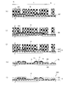
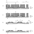
- (A)-(g) is sectional drawing for demonstrating an example of the manufacturing method of 100 A of semiconductor devices by embodiment of this invention.
- (H) to (l) are cross-sectional views for explaining an example of the manufacturing method of the semiconductor device 100A according to the embodiment of the present invention.
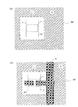
- (A) And (b) is a top view for demonstrating an example of the manufacturing method of 100 A of semiconductor devices by embodiment of this invention, and respond
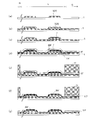
- (A)-(g) is sectional drawing for demonstrating the other example of the manufacturing method of 100 A of semiconductor devices by embodiment of this invention.
- (H) to (k) are cross-sectional views for explaining another example of the manufacturing method of the semiconductor device 100A according to the embodiment of the present invention.
- (A) And (b) is a top view for demonstrating an example of the manufacturing method of 100 A of semiconductor devices by embodiment of this invention, and respond
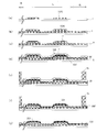
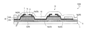
- (A)-(g) is sectional drawing for demonstrating the further another example of the manufacturing method of 100 A of semiconductor devices by embodiment of this invention. It is sectional drawing which shows the semiconductor device 100B of 2nd Embodiment by this invention. It is sectional drawing which shows 100 C of semiconductor devices of 3rd Embodiment by this invention.
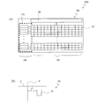
- (A) is a top view which shows semiconductor device 100D of 4th Embodiment by this invention,
- (b) is a figure explaining the structure of each pixel 101 in semiconductor device 100D.
- (A) is a block diagram showing the configuration of the shift register 110A in the gate driver circuit of the semiconductor device 100D, and (b) is a diagram illustrating the circuit configuration of each stage of the shift register 110A. It is a figure for demonstrating the layout of 110 A of shift registers. It is sectional drawing which illustrates the display apparatus 1000 of embodiment by this invention.
- a semiconductor device 100A according to a first embodiment of the present invention will be described with reference to FIG.
- the semiconductor device 100A exemplified here is a TFT substrate having a plurality of TFTs on the substrate.
- the TFT substrate can be used in a display device such as a liquid crystal display device or an organic EL display device.
- the semiconductor device 100A of the present embodiment is not limited to a TFT substrate as long as it includes a plurality of TFTs.
- 1A and 1B are a cross-sectional view and a plan view showing a part of the semiconductor device 100A, respectively.
- the semiconductor device 100A includes a substrate 1, a plurality of TFTs 10 supported by the substrate 1, a global wiring 9g, a gate metal layer 20 including the gate electrode 3 of the TFT 10, source and drain electrodes 9s and 9d of the TFT 10, and a global wiring.
- the “global wiring 9 g” refers to a wiring that supplies a common signal to the plurality of TFTs 10.
- the semiconductor device (TFT substrate) 100A has a display area including a plurality of pixels. Each pixel is provided with a TFT (pixel TFT) as a switching element.
- the TFT substrate may be provided with part or all of a driver circuit such as a driver (monolithic).
- the drive circuit is formed in a region (non-display region) other than the display region on the TFT substrate.
- the TFT 10 illustrated in FIG. 1 may be disposed for each pixel as a pixel TFT.
- the global wiring 9g may be a source bus line.
- the TFT 10 may be arranged in a non-display area as a TFT (circuit TFT) constituting a circuit such as a shift register, and the global wiring 9g may be a wiring (for example, a trunk wiring) constituting the circuit. Furthermore, both the pixel TFT and the circuit TFT may be the TFT 10. A more specific configuration of the semiconductor device 100A will be described later.
- the TFT 10 has a bottom gate structure.
- the TFT 10 is provided on the gate electrode 3, the gate insulating layer 5 formed on the gate electrode 3, the semiconductor layer 7 formed on the gate insulating layer 5, and the semiconductor layer 7.
- Source electrode 9s and drain electrode 9d electrically connected to each other.
- the source electrode 9s and the drain electrode 9d are formed so as to be in contact with portions of the upper surface of the semiconductor layer 7 located on both sides of the channel region 7c.
- the surface of the channel region 7 c is in contact with the insulating protective layer 12.
- at least the channel region 7 c of the semiconductor layer 7 is disposed so as to overlap the gate electrode 3 with the gate insulating layer 5 interposed therebetween.
- the global wiring 9g is electrically connected to the plurality of TFTs 10.
- the global wiring 9g is formed integrally with the source electrode 9s of the TFT 10.
- the gate metal layer 20 refers to a layer including electrodes formed by patterning a conductive film forming the gate electrode 3 of the TFT 10, wiring such as gate bus lines, terminals, and the like.
- the gate metal layer 20 may include a CS bus line and a CS electrode (not shown) in addition to the gate electrode 3 and the gate bus line.
- the source metal layer 30 refers to a layer including electrodes formed by patterning a conductive film that forms the source electrode 9s and the drain electrode 9d, wiring such as source bus lines, terminals, and the like.
- the source metal layer 30 is, for example, a drain extraction wiring / electrode (not shown) (a wiring / electrode that faces the CS bus line or the CS electrode and forms a CS capacitor). Etc. may be included.
- wirings constituting the drive circuit and circuit element electrodes may be included.
- the source metal layer 30 includes a source electrode 9s and a drain electrode 9d, and a global wiring 9g.
- an inter-transistor connection wiring 9 a that connects two TFTs 10
- a global wiring-inter-transistor connection wiring 9 b that connects the global wiring 9 g and the TFT 10, and the like may be included.
- the source metal layer 30 of the present embodiment includes a lower layer 30A and an upper layer 30B stacked on a part of the lower layer 30A. Accordingly, the source metal layer 30 has a portion including the lower layer 30A and the upper layer 30B and a portion including the lower layer 30A but not the upper layer 30B.
- a wiring structure including the lower layer 30A and the upper layer 30B is referred to as a “first layer structure”, and a wiring structure including the lower layer 30A and not including the upper layer 30B is referred to as a “second layer structure”.
- Each of the lower layer 30A and the upper layer 30B may be a single layer or may have a stacked structure of two or more layers.
- the surface of the upper layer 30B in the first layer structure may be in contact with the insulating protective layer 12, and the surface of the lower layer 30A in the second layer structure may be in contact with the insulating protective layer 12.
- the global wiring 9g in the present embodiment has a first layer structure.
- at least a portion of the source electrode 9s and the drain electrode 9d located on the semiconductor layer 7 of the TFT 10 has a second layer structure.
- at least a portion of the source electrode 9s and the drain electrode 9d located on the semiconductor layer 7 of the TFT 10 is composed of only the lower layer 30A, and the global wiring 9g includes the lower layer 30A and the upper layer 30B. It is composed of Therefore, the insulating protective layer 12 is in contact with the lower layer 30A on the semiconductor layer 7, and the upper layer 30B of the global wiring 9g is in contact with the insulating protective layer 12.
- the semiconductor device 100A has three or more TFTs, at least two of them may have the above-described configuration. Further, in the semiconductor device 100A, it is only necessary that at least a part of the wiring for supplying a common signal to the plurality of TFTs 10 has the above-described wiring structure.
- the thickness and material of the global wiring 9g and the thickness and material of the source electrode 9s and the drain electrode 9d on the semiconductor layer 7 can be controlled independently of each other. Therefore, it is possible to improve the coverage of the insulating protective layer 12 with respect to the TFT 10 while keeping the resistance of the global wiring 9g low.
- the structure of the source metal layer 30 can be partially different. For this reason, it is possible to individually optimize the structure of the electrodes, wirings, and the like in the source metal layer 30 according to the application, the position where they are formed, and the like.
- the source electrode 9s and the drain electrode 9d on the semiconductor layer 7 can be formed thinner than the global wiring 9g. Accordingly, it is possible to suppress a decrease in coverage such as generation of voids in the insulating protective layer 12 due to a step between the source electrode 9s and the drain electrode 9d while suppressing the resistance of the global wiring 9g. As a result, it is possible to suppress degradation of TFT characteristics due to impurities and moisture entering the semiconductor layer 7.
- the width of the gate electrode 3 in the channel length direction is larger than the width of the semiconductor layer 7 in the channel length direction.
- at least a portion of the source electrode 9s and the drain electrode 9d that overlaps with the gate electrode 3 may have a second layer structure.
- the global wiring 9g can be formed without increasing the thickness of the source electrode 9s and the drain electrode 9d on the semiconductor layer 7. It becomes possible to increase the thickness of the conventional one. Therefore, it is possible to further reduce the wiring resistance and improve the circuit performance while ensuring the coverage of the insulating protective layer 12.
- the source electrode 9s and the drain electrode 9d of the TFT 10 may be configured by only the lower layer 30A, and the upper layer 30B may not configure the TFT 10.
- the lower layer 30A may be extended to the outside of the TFT 10 (outside of the semiconductor layer 7 of the TFT 10 and a region in the vicinity thereof) and used for connection to another TFT or wiring. Thereby, the deterioration of the TFT 10 due to a decrease in the coverage of the insulating protective layer 12 can be more effectively suppressed.
- the source electrode 9s refers to a portion of the source metal layer 30 that overlaps the semiconductor layer 7 when viewed from the normal direction of the substrate 1 and functions as the source of the TFT 10, and the drain electrode 9d is the source metal layer Of the layer 30, it may refer to a portion that overlaps with the semiconductor layer 7 when viewed from the normal direction of the substrate 1 and functions as the drain of the TFT 10.
- the above-mentioned “outside of TFT 10” refers to a region other than the region (TFT region) defined by the semiconductor layer 7, the source electrode 9 s and the drain electrode 9 d when viewed from the normal direction of the substrate 1. .
- a TFT having a channel etch structure is used as the TFT 10.
- the etching step for example, a conductive film is deposited on the surface of the semiconductor layer, and anisotropic etching of the conductive film is performed to separate the source electrode and the drain electrode.
- the conductive film becomes thicker, variation in the thickness of the conductive film increases, and thus the amount of removal of the portion that becomes the channel region of the semiconductor layer by anisotropic etching (overetching amount) increases.
- the “over-etching amount” refers to the amount of the semiconductor material that is the underlying material that is exposed to etching after the conductive material that is the material to be etched is removed.
- the amount of over-etching increases, damage to the semiconductor layer also increases, and there is a possibility that stable TFT characteristics cannot be obtained.
- characteristic deterioration due to damage received in the etching process is significant.
- the conductive film formed on the semiconductor layer 7 can be made thinner than before, the amount of overetching of the semiconductor layer 7 can be reduced in the etching process for forming the source electrode 9s and the drain electrode 9d. Can be suppressed. Therefore, since damage to the semiconductor layer 7 can be reduced, deterioration of TFT characteristics can be suppressed.
- the thickness of the source electrode 9s and the drain electrode 9d on the semiconductor layer 7, that is, the thickness t A of the lower layer 30A is, for example, 200 nm or less, more preferably 100 nm or less. Thereby, the fall of the coating property of the insulating protective layer 12 can be suppressed more reliably. In addition, damage to the semiconductor layer 7 due to anisotropic etching can be reduced more effectively. On the other hand, if the thickness t A of the lower layer 30A is 300 nm or more, for example, the resistance of the TFT can be further reduced.
- the thickness of the global wiring 9g that is, the total thickness t B of the lower layer 30A and the upper layer 30B is, for example, 300 nm or more, more preferably 400 nm or more. As a result, the resistance of the global wiring 9g can be kept lower, so that the operation speed of the circuit including the TFT 10 can be increased more effectively.
- the thickness t B is preferably 500 nm or less.
- the thickness of the lower layer 30A in the first layer structure and the thickness of the lower layer 30A in the second layer structure are substantially the same.
- the surface layer of the lower layer 30A may also be removed.
- the lower layer 30A in the first layer structure is thicker than the lower layer 30A in the second layer structure.
- the lower layer 30A may be thinner than the upper layer 30B. Thereby, it is possible to more effectively reduce the resistance of the global wiring 9g and suppress the deterioration of the TFT characteristics.
- the thickness of the upper layer 30B may be, for example, not less than 2 times and not more than 10 times the thickness of the lower layer 30A.
- both the inter-transistor connection wiring 9a and the global wiring-inter-transistor connection wiring 9b have the second layer structure. Note that some of these connection wirings 9a and 9b may have a first layer structure.
- the wiring structure of the connection wirings 9a and 9b can be appropriately selected according to the distance from the closest TFT 10.
- the inter-transistor connection wiring 9a has the second layer structure, it is not necessary to partially form the upper layer 30B between the adjacent TFTs 10. Therefore, it is not necessary to increase the distance D between the adjacent TFTs 10 in consideration of the design margin by lithography. Therefore, compared to the case where the inter-transistor connection wiring 9a has the first layer structure, the adjacent TFTs 10 The distance D between them can be reduced.
- the distance D here refers to the shortest distance between the two semiconductor layers 7 when viewed from the normal direction of the surface of the substrate 1.
- the source metal layer 30 preferably has the second layer structure.
- the portion having the first layer structure of the source metal layer 30 is provided in the vicinity of the semiconductor layer 7, the coverage of the insulating protective layer 12 is reduced due to the step generated at the end of the upper layer 30 ⁇ / b> B.
- the distance E is, for example, 3 ⁇ m or more, more preferably 10 ⁇ m or more.
- the distance E can be appropriately selected depending on the process margin, the thickness of the upper layer 30B, the material of the insulating protective layer 12, and the like.
- the upper layer 30B is located on a region that is sufficiently separated from the TFT 10 and in which the effect of the step due to the semiconductor layer 7 and the gate electrode 3 is reduced, for example, on a region where the surface of the gate insulating layer 5 is substantially flat. Has been placed. Thereby, the penetration
- the lower layer 30A may include a first layer
- the upper layer 30B may include a second layer formed on the first layer using a material different from that of the first layer.
- patterning for forming the lower layer 30A and the upper layer 30B can be performed using the difference in etching rate.
- the lower layer 30A may be composed of only the first layer, or may further include another layer below the first layer (substrate side).
- the upper layer 30B may be composed of only the second layer, or may further have another layer on the second layer.
- the semiconductor device 100A of the present embodiment includes a global wiring region G including the global wiring 9g and a local wiring region L including the TFT 10, and a portion of the source metal layer 30 located in the global wiring region G is the first.
- the layer structure and the portion located in the local wiring region L may have a second layer structure.
- the local wiring region L is disposed in a region including the TFT 10 and the vicinity thereof, and the global wiring region G is disposed in a region other than the TFT 10 and the vicinity thereof.
- a region where a plurality of TFTs 10 are arranged close to each other may be referred to as a local wiring region L, and a region located between the plurality of local wiring regions L may be referred to as a global wiring region G.
- the global wiring region G is preferably separated from the semiconductor layer 7 of the closest TFT 10 by, for example, 5 ⁇ m or more.
- the distance between the semiconductor layer 7 of the TFT 10 and the end portion of the upper layer 30B in the substrate plane. Can be ensured sufficiently, so that a decrease in the coverage of the insulating protective layer 12 in the vicinity of the semiconductor layer 7 can be more reliably suppressed.
- the arrangement of the local wiring region L and the global wiring region G can be appropriately selected depending on the configuration of the circuit including the TFT 10, the distance between the semiconductor layer 7 of the TFT 10 and the global wiring 9g, and the like.
- the case where the source metal layer 30 has the pattern shown in FIG. 1B will be described as an example.
- the wiring protruding from the global wiring 9g when viewed from the normal direction of the substrate 1 The local wiring region L may be arranged so as to include the entire (protruding portion).
- the local wiring region L may be arranged so as to include only a part of the protruding portion.
- the portion close to the global wiring 9g in the protruding portion has the first layer structure
- the portion close to the TFT 10 has the second layer structure.
- the local wiring region L may be arranged so as to include a part of the global wiring 9g.
- the local wiring region L may be arranged so as to cross the global wiring 9g (for example, the source bus line).
- the upper layer 30B is divided in the global wiring 9g, and the portion where the upper layer 30B is divided is composed of only the lower layer 30A.
- the global wiring region G and the local wiring region L may be arranged so as to partially overlap.
- FIGS. 4 (h) to 4 (l) are process cross-sectional views for explaining a method for manufacturing the semiconductor device 100A.
- 5 (a) and 5 (b) are plan views corresponding to FIGS. 3 (g) and 4 (h), respectively.
- a gate metal layer 20 including a gate electrode 3, a gate bus line (not shown) and a connection wiring (not shown) is formed on a substrate 1 such as a glass substrate.
- the gate metal layer 20 is formed on the substrate 1 by forming a gate conductive film (not shown) using a sputtering method and patterning the gate conductive film using a mask.
- the substrate 1 is typically a transparent substrate, for example, a glass substrate.
- a plastic substrate can also be used.
- the plastic substrate may be a substrate formed of a thermosetting resin or a thermoplastic resin, or a composite substrate of these resins and inorganic fibers (for example, glass fibers or glass fiber nonwoven fabrics).
- a resin material having heat resistance polyethylene terephthalate (PET), polyethylene naphthalate (PEN), polyethersulfone (PES), acrylic resin, or polyimide resin can be used.
- a metal such as aluminum (Al), molybdenum (Mo), copper (Cu), titanium (Ti), an alloy including at least one of these, or a metal nitride thereof is used.
- a metal such as aluminum (Al), molybdenum (Mo), copper (Cu), titanium (Ti), an alloy including at least one of these, or a metal nitride thereof is used.
- a Ti / Al / Ti film thickness: for example, 100 nm to 500 nm
- the gate conductive film is used as the gate conductive film.
- the gate insulating layer 5 is formed so as to cover the gate metal layer 20.
- the gate insulating layer 5 is formed using, for example, a CVD method.
- Examples of the material of the gate insulating layer 5 include silicon oxide (SiO x ), silicon nitride (SiN x ), silicon oxynitride (SiO x N y , x> y), and silicon nitride oxide (SiN x O y , x>).
- y silicon nitride oxide
- the gate insulating layer 5 may be a single layer film or a laminated film.
- the gate insulating layer 5 is a SiO 2 film having a thickness of 100 nm to 500 nm, for example.
- an island-shaped semiconductor layer 7 is formed. Specifically, first, an oxide semiconductor film (not shown) is formed on the gate insulating layer 5 by sputtering.
- the oxide semiconductor film for example, an In—Ga—Zn—O-based oxide semiconductor film with a thickness of 30 nm to 300 nm is formed. Thereafter, the oxide semiconductor film is patterned by photolithography to obtain an island-shaped semiconductor layer (here, an oxide semiconductor layer) 7.
- the oxide semiconductor film and the semiconductor layer 7 include, for example, an In—Ga—Zn—O-based semiconductor.
- the In—Ga—Zn—O-based semiconductor may be amorphous or crystalline.
- a crystalline In—Ga—Zn—O-based semiconductor As the crystalline In—Ga—Zn—O-based semiconductor, a crystalline In—Ga—Zn—O-based semiconductor in which the c-axis is oriented substantially perpendicular to the layer surface is preferable.
- Such a crystal structure of an In—Ga—Zn—O-based semiconductor is disclosed in, for example, Japanese Patent Laid-Open No. 2012-134475.
- the entire disclosure of Japanese Patent Application Laid-Open No. 2012-134475 is incorporated herein by reference.
- materials of the oxide semiconductor film include oxide semiconductors other than In—Ga—Zn—O-based semiconductors, such as InGaO 3 (ZnO) 5 , magnesium zinc oxide (Mg x Zn 1-x O), and cadmium zinc oxide ( Cd x Zn 1-x O) or cadmium oxide (CdO) may be used.
- ZnO to which one or more impurity elements of Group 1 element, Group 13 element, Group 14 element, Group 15 element or Group 17 element are added, or an amorphous state, a polycrystalline state, or A microcrystalline state in which an amorphous state and a polycrystalline state are mixed, or a state in which no impurity element is added can also be used.
- another semiconductor film such as a silicon semiconductor film may be used instead of the oxide semiconductor film.
- the first conductive film 30A ′ and the second conductive film 30B ′ are formed in this order on the gate insulating layer 5 and the semiconductor layer 7 by, eg, sputtering. Then, a source conductive film 30 ′ having a laminated structure (here, a two-layer structure) is formed.
- the material for the first conductive film 30A ′ and the second conductive film 30B ′ include aluminum (Al), tungsten (W), molybdenum (Mo), tantalum (Ta), copper (Cu), chromium (Cr), and titanium.
- a film containing a metal such as (Ti) or an alloy thereof, or a metal nitride thereof can be used as appropriate.
- Each of the conductive films 30A 'and 30B' may be a single layer film or a laminated film.
- the second conductive film 30B ′ is easily obtained. Can be patterned. Further, the thickness of the first conductive film 30A 'may be smaller than the thickness of the second conductive film 30B'. Thereby, the part which has a 1st layer structure among source metal layers can be made thinner. Further, the sheet resistance of the second conductive film 30B 'may be lower than the sheet resistance of the first conductive film 30A'. As a result, the resistance of the global wiring can be further reduced, so that the circuit characteristics can be improved.
- a Ti film having a thickness of 20 to 150 (eg, 70 nm) is formed as the first conductive film 30A ′, and an Al film having a thickness of from 100 nm to 500 nm (eg, 300 nm) is formed as the second conductive film 30B ′.
- a film is formed.
- a first photoresist 51 is formed on the source conductive film 30 'using a first mask.
- the first photoresist 51 is disposed so as to cover at least a portion to be a global wiring and not to cover the semiconductor layer 7.
- the region covered with the first photoresist 51 corresponds to the global wiring region G for forming the wiring and electrodes having the first layer structure
- the region not covered with the first photoresist 51 is the region covered with the first photoresist 51.
- the mask data of the first mask is designed so as to correspond to the local wiring region L in which the TFT and the wiring and electrode having the second layer structure are formed.
- the portion of the second conductive film 30B 'that is not covered with the first photoresist 51 is removed by a dry etching method or a wet etching method. Regardless of which etching method is used, the materials and etching methods of these films 30A ′ and 30B ′ are adjusted so that the etching rate of the first conductive film 30A ′ is lower than the etching rate of the second conductive film 30B ′. select. Accordingly, in the region not covered with the first photoresist 51, only the second conductive film 30B 'is patterned, and the first conductive film 30A' is hardly etched.
- FIG. 3G A plan view corresponding to FIG. 3G is shown in FIG.
- the second conductive film 30 ⁇ / b> B ′ is formed over the global wiring region G.
- the second conductive film 30B ' is removed, and the upper surface of the first conductive film 30A' is exposed.
- a second photoresist 52 is formed on the source conductive film 30 'using the second mask.
- the second mask defines the pattern of the wiring (local wiring) such as the TFT drain electrode and source electrode and the inter-transistor connection wiring in the local wiring region L, and in the global wiring region G, It is designed to define a pattern of wiring having a first layer structure such as global wiring.
- the pattern of the second photoresist 52 is illustrated in FIG.
- the portion of the second conductive film 30B 'that is not covered with the second photoresist 52 is removed by a dry etching method or a wet etching method. Regardless of which etching method is used, the materials and etching methods of these films 30A ′ and 30B ′ are adjusted so that the etching rate of the first conductive film 30A ′ is lower than the etching rate of the second conductive film 30B ′. select. Accordingly, even in a region not covered with the second photoresist 52, only the second conductive film 30B 'is patterned, and the first conductive film 30A' is hardly etched.
- the second conductive film 30B ' is patterned, and the upper layer 30B used for the global wiring is obtained.
- the first conductive film 30A is formed in the opening portion of the second photoresist 52. 'Is exposed. In this etching process, the exposed first conductive film 30A 'is not patterned.
- the part used as the channel region of the semiconductor layer 7 is covered with 1st electrically conductive film 30A ', it can suppress that the part used as a channel region receives a damage by this etching process.
- the portion of the first conductive film 30A ′ that is not covered with the second photoresist 52 is etched using the second photoresist 52 again as an etching mask. Remove with.
- an etching method for example, a dry etching method such as an RIE (reactive ion etching) method or a wet etching method is used.
- the lower layer 30A is obtained from the first conductive film 30A '. In this way, the source metal layer 30 including the lower layer 30A and the upper layer 30B is obtained.
- the source electrode 9s and the drain electrode 9d composed of the lower layer 30A are obtained, and thus the TFT 10 is manufactured. Further, a local wiring composed of the lower layer 30A, such as the inter-transistor connection wiring 9a, is formed.
- a global wiring 9g having a laminated structure (first layer structure) of the lower layer 30A and the upper layer 30B is formed. Thereafter, as shown in FIG. 4K, the second photoresist 52 is removed.
- an insulating protective layer (passivation layer) 12 covering the TFT 10 and the source metal layer 30 is provided using, for example, a CVD apparatus.
- the insulating protective layer 12 is made of SiO x , SiN x , SiO x N y (silicon oxynitride, x> y), SiN x O y (silicon nitride oxide, x> y), Al 2 O 3 (aluminum oxide) or Ta It may be made of 2 O 5 (tantalum oxide) or the like.
- the thickness of the insulating protective layer 12 is not particularly limited, but is, for example, 100 nm or more and 300 nm or less.
- a SiO 2 film is formed by a plasma CVD method.
- planarizing film may be formed on the insulating protective layer 12.
- the planarizing film can be obtained, for example, by applying a photosensitive organic film on the insulating protective layer 12 and curing it. In this way, the semiconductor device 100A is manufactured.
- the drain electrode 9d and the source electrode 9s of the TFT 10 can be formed only from the first conductive film 30A ', and the step generated in the base of the insulating protective layer 12 in the vicinity of the TFT 10 can be reduced. As a result, deterioration of the covering property of the insulating protective layer 12 in the vicinity of the TFT 10 can be suppressed. Further, in the etching process (source / drain separation process) for forming the source electrode 9s and the drain electrode 9d, only the first conductive film 30A ′ is patterned, so that the portion that becomes the channel of the semiconductor layer 7 at the time of patterning Can reduce the damage to the. This effect is particularly remarkable when the thickness of the first conductive film 30A 'is small.
- the thickness of the global wiring 9g can be arbitrarily set independently of the thicknesses of the source electrode 9s, the drain electrode 9d, the local wiring, and the like. Accordingly, the thickness of the global wiring 9g can be increased, and a low resistance wiring can be realized.
- the manufacturing method of the semiconductor device 100A of the present embodiment is not limited to the above method. Hereinafter, another example of the manufacturing method of the semiconductor device 100A will be described.
- FIGS. 6A to 6G and FIGS. 7H to 7K are process cross-sectional views for explaining another method for manufacturing the semiconductor device 100A.
- FIGS. 8A and 8B are plan views corresponding to FIGS. 6G and 7H, respectively. Components similar to those in FIGS. 3 to 5 are denoted by the same reference numerals and description thereof is omitted.
- a gate metal layer 20 including a gate electrode 3, a gate insulating layer 5, and an island-shaped semiconductor layer 7 serving as an active layer of a TFT are formed on a substrate 1.
- the first conductive film 30 ⁇ / b> A ′ and the second conductive film 30 ⁇ / b> B ′ are formed in this order on the gate insulating layer 5 and the semiconductor layer 7, thereby forming the source conductive film 30 ′.
- These forming methods are the same as those described above with reference to FIGS. 3 (a) to 3 (d).
- the material and thickness of each layer are the same as those described above.
- a third photoresist 53 is formed on the source conductive film 30 'using a third mask.
- the third photoresist 53 is designed to define a pattern of wiring having a first layer structure such as global wiring.
- the portion of the second conductive film 30B 'that is not covered with the third photoresist 53 is removed by etching.
- the etching method is the same as the method described above with reference to FIG. Thereby, the upper layer 30B is obtained from the second conductive film 30B '.
- FIG. 6G A plan view corresponding to FIG. 6G is shown in FIG.
- the upper layer 30B is formed in the region where the wiring having the first layer structure such as the global wiring is formed, and in the other regions, the first layer 30B is formed.
- the upper surface of the conductive film 30A ′ is exposed.
- a fourth photoresist 54 is formed on the source conductive film 30 'using a fourth mask.
- the fourth mask defines the pattern of the wiring (local wiring) such as the TFT drain electrode and source electrode and the inter-transistor connection wiring in the local wiring region L, and in the global wiring region G, It is designed to define a pattern of wiring having a first layer structure such as global wiring.
- the pattern of the fourth photoresist 54 is illustrated in FIG. As shown in the drawing, the first conductive film 30 ⁇ / b> A ′ is exposed in the opening portion of the fourth photoresist 54.
- the portion of the first conductive film 30A 'that is not covered with the fourth photoresist 54 is removed by a dry etching method or a wet etching method.
- the lower layer 30A is obtained from the first conductive film 30A '.
- the source metal layer 30 including the lower layer 30A and the upper layer 30B is obtained.
- the source electrode 9s and the drain electrode 9d composed of the lower layer 30A are obtained, and thus the TFT 10 is manufactured. Further, a local wiring composed of the lower layer 30A, such as the inter-transistor connection wiring 9a, is formed.
- a global wiring 9g having a laminated structure (first layer structure) of the lower layer 30A and the upper layer 30B is formed. Thereafter, as shown in FIG. 7J, the second photoresist 52 is removed.
- an insulating protective layer (passivation layer) 12 covering the TFT 10 and the source metal layer 30 is provided.
- the material, thickness and formation method of the insulating protective layer 12 are the same as those described above with reference to FIG. Thereafter, although not shown, a planarizing film may be formed on the insulating protective layer 12. In this way, the semiconductor device 100A is manufactured.
- a multi-tone mask may be used as the second mask.
- a halftone mask is used instead of the second mask.
- 9A to 9G are process cross-sectional views for explaining still another example of the method for manufacturing the semiconductor device 100A.
- a gate metal layer 20 including a gate electrode 3, a gate insulating layer 5, a semiconductor layer 7, a first conductive film 30A ′ and a second conductive film 30B ′ are formed on a substrate 1.
- a portion of the second conductive film 30B 'located in the local wiring region L is removed using a first photoresist.
- the method for forming these layers and the method for etching the second conductive film 30B ' are the same as those described above with reference to FIGS.
- the material and thickness of each layer (or film) are the same as those described above.
- a fifth photoresist 55 is formed on the source conductive film 30 'using the fifth mask.
- a multi-tone mask is used as the fifth mask.
- a region exposed at three different exposure amounts can be obtained in one exposure step.
- the fifth photoresist 55 can be formed by developing and developing this.
- a region where the exposure amount is an intermediate value is defined by a halftone mask.
- a photoresist film is formed using a negative type photoresist an opening is formed in a region where the exposure amount is the largest, a region where the exposure amount is the smallest, and a recess ( A portion thinner than the region with the maximum exposure amount) is formed.
- a positive photoresist is used, the film thickness of the region with the smallest exposure amount is the largest, an opening is formed in the region with the largest exposure amount, and a recess is formed in the region with the intermediate exposure amount.
- the fifth mask defines the pattern of wiring (local wiring) such as the TFT drain electrode and source electrode and inter-transistor connection wiring in the local wiring region L, and in the global wiring region G, the global wiring or the like. It is designed to define the pattern of the wiring having the first layer structure. Further, the region where the exposure amount is intermediate is designed to define a region x in the local wiring region L where the pattern of the wiring (local wiring) such as the drain electrode and source electrode of the TFT and the inter-transistor connection wiring is not formed. Yes.
- the fifth photoresist 55 obtained by development has a recess in the region x in the local wiring region L. That is, it is thinner than the region that defines the electrode and wiring patterns.
- the global wiring region G has an opening in a region y where a wiring pattern is not formed.
- the portion of the second conductive film 30B ′ that is not covered with the fifth photoresist 55, that is, the portion located in the region y is removed by the dry etching method or the wet etching method. To do. Regardless of which etching method is used, the materials and etching methods of these films 30A ′ and 30B ′ are adjusted so that the etching rate of the first conductive film 30A ′ is lower than the etching rate of the second conductive film 30B ′. select. Accordingly, only the second conductive film 30B 'that is not covered with the fifth photoresist 55 is patterned, and the first conductive film 30A' is hardly etched. Thereby, in the global wiring region G, the second conductive film 30B 'is patterned, and the upper layer 30B used for the global wiring is obtained.
- the local wiring region L is covered with the fifth photoresist 55.
- the pattern of local wiring such as TFT source and drain electrodes and inter-transistor connection wiring is covered with a thick portion of the fifth photoresist 55, and the region (x) other than the above pattern is the fifth photoresist 55. It is covered with a thin part. For this reason, the portion of the first conductive film 30A 'located in the local wiring region L is not patterned in this etching process, and is not exposed to the etching atmosphere.
- the thickness of the fifth photoresist 55 is decreased by performing the ashing process using the fifth photoresist 55 as it is.
- the thin portion of the fifth photoresist 55 located in the region x is removed, and the first conductive film 30A 'is exposed.
- the fifth photoresist 55 after the ashing process has openings in the region x and the region y.
- the exposed part) is removed by etching.
- etching method for example, a drain etching method or a wet etching method is used.
- a drain etching method or a wet etching method is used.
- portions of the first conductive film 30A 'located in the region x and the region y are removed, and the lower layer 30A is formed. In this way, the source metal layer 30 including the lower layer 30A and the upper layer 30B is obtained.
- the source electrode 9s and the drain electrode 9d constituted by the lower layer 30A are obtained, whereby the TFT 10 is manufactured. Further, a local wiring composed of the lower layer 30A, such as the inter-transistor connection wiring 9a, is formed.
- a global wiring 9g having a laminated structure (first layer structure) of the lower layer 30A and the upper layer 30B is formed. Thereafter, as shown in FIG. 9F, the fifth photoresist 55 is removed.
- an insulating protective layer (passivation layer) 12 covering the TFT 10 and the source metal layer 30 is provided.
- the material, thickness and formation method of the insulating protective layer 12 are the same as those described above with reference to FIG. Thereafter, although not shown, a planarizing film may be formed on the insulating protective layer 12. In this way, the semiconductor device 100A is manufactured.
- etching for forming the upper layer 30B is performed in a state where the portion to be the channel of the semiconductor layer 7 is covered with both the first conductive film 30A ′ and the fifth photoresist 55. be able to. Accordingly, the first conductive film 30A 'is less likely to be damaged in the etching atmosphere, so that it becomes possible to more reliably protect the portion that becomes the channel region of the semiconductor layer 7.
- FIG. 10 is a cross-sectional view illustrating a semiconductor device 100B according to the second embodiment of the invention.
- the semiconductor device 100B is different from the semiconductor device 100A shown in FIG. 1 in that it has an etch stop layer that covers the channel region of the semiconductor layer.
- FIG. 10 the same components as those in FIG.
- the semiconductor device 100B includes an etch stop layer 8 between the semiconductor layer 7 and the source electrode 9s and the drain electrode 9d.
- the etch stop layer 8 is provided so as to cover at least the channel region 7 c of the semiconductor layer 7.
- the etch stop layer 8 may be a silicon oxide film, a silicon nitride film, a silicon oxynitride film, or a laminated film thereof.
- the thickness of the etch stop layer 8 is, for example, not less than 50 nm and not more than 400 nm.
- the source electrode 9s and the drain electrode 9d are disposed so as to be in contact with a portion of the surface of the semiconductor layer 7 that is not covered with the etch stop layer 8.
- the source electrode 9s and the drain electrode 9d may be in contact with the semiconductor layer 7 in the opening formed in the etch stop layer 8, respectively. Further, the etch stop layer 8 may be extended over substantially the entire substrate 1 as with the gate insulating layer 5. Since other configurations are the same as those of the semiconductor device 100A, description thereof is omitted.
- the same effect as that of the first embodiment can be obtained. Specifically, the deterioration of the TFT characteristics due to the decrease in the coverage of the insulating protective layer 12 can be suppressed. Further, the circuit characteristics can be improved by suppressing the resistance of the global wiring 9g.
- the etching process for forming the source electrode 9s and the drain electrode 9d the portion that becomes the channel region of the semiconductor layer 7 is protected by the etch stop layer 8. Therefore, as compared with the first embodiment, the damage received by the semiconductor layer 7 by etching can be more reliably suppressed.
- the semiconductor device 100B can be manufactured by the same method as the semiconductor device 100A except that the etch stop layer 8 is formed after the patterning of the semiconductor layer 7 and before the formation of the source conductive film 30 ′.
- the etch stop layer 8 can be formed, for example, by forming a silicon oxide film (SiO 2 film) so as to cover the semiconductor layer 7 by CVD and patterning the silicon oxide film.
- the TFT 10 shown in FIG. 1 is used as the pixel TFT in the active matrix substrate (TFT substrate) of the liquid crystal display device.
- FIG. 11 is a plan view illustrating a part of the TFT substrate 100C, and shows a part of the display area of the TFT substrate 100C.
- the TFT substrate 100 ⁇ / b> C has a display area including a plurality of pixels 101.
- a plurality of source bus lines 31 formed on an insulating substrate, a plurality of gate bus lines 21, a plurality of TFTs (pixel TFTs) 10 formed at intersections thereof, and each pixel A pixel electrode 41 formed on the pixel 101 is provided.
- Each pixel 101 may be provided with an auxiliary capacitor (not shown).
- the TFT 10 has a configuration as shown in FIG.
- the source electrode 9 s of each TFT 10 is electrically connected to the source bus line 31, the gate electrode 3 is electrically connected to the gate bus line 21, and the drain electrode 9 d is electrically connected to the pixel electrode 41.
- the pixel electrode 41 is made of, for example, a transparent conductive film (for example, ITO (Indium Tin Oxide) or IZO (registered trademark) (Indium Zinc Oxide) film).
- the thickness of the pixel electrode 41 is, for example, not less than 20 nm and not more than 200 nm.
- the source bus line 31 extends in a direction orthogonal to the gate bus line 21.
- the source bus line 31 and the source electrode 9 s are connected by a wiring 9 b extending from the side surface of the source bus line 31 in a direction different from that of the source bus line 31.
- the source bus line 31 is a global wiring 9g and has a first layer structure.
- the wiring 9b, the source electrode 9s and the drain electrode 9d have a second layer structure. As described above, it is only necessary that the portion of the source electrode 9s and the drain electrode 9d located on the semiconductor layer 7 has at least the second layer structure, and the wiring 9b, the source electrode 9s, and the drain electrode 9d
- the structure is not limited to the above.
- the TFT 10 shown in FIG. 1 is used as a pixel TFT, but an etch stop type TFT as shown in FIG. 10 may be used instead.
- the circuit TFT used in the peripheral circuit may have the same structure as the pixel TFT described above.
- a part of the wiring in the peripheral circuit may have the same wiring structure (first layer structure) as that of the source bus line 31.
- the active matrix substrate of the liquid crystal display device has been described as an example here, but the present invention can also be applied to an active matrix substrate of another display device such as an organic EL display device.
- the TFT 10 shown in FIG. 1 is used as a circuit TFT in an active matrix substrate (TFT substrate) of a liquid crystal display device.
- FIG. 12A is a schematic plan view showing the TFT substrate 100D of the present embodiment.
- the TFT substrate 100D has a display area 130 including a plurality of pixels 101 and an area (non-display area) 140 other than the display area.
- a gate driver 110 and a source driver 120 are provided in the non-display area 140.
- the gate driver 110 is formed integrally with the TFT substrate 100D.
- the source driver 120 may not be integrally formed, and a separately manufactured source driver IC or the like may be mounted on the TFT substrate 100D by a known method.
- FIG. 12B shows the configuration of the pixel 101 on the TFT substrate 100D.
- the pixel 101 includes a pixel TFT, a source bus line 31, a gate bus line 21, and a pixel electrode 41.
- the drain electrode of the pixel TFT is connected to the pixel electrode 41, and the source electrode is connected to the source bus line 31.
- the gate electrode of the pixel TFT is connected to the gate bus line 21.
- the gate bus line 21 is connected to the output of the gate driver 110 and is scanned line-sequentially.
- the source bus line 31 is connected to the output of the source driver 120 and supplied with a display signal voltage (gray scale voltage).
- FIG. 13A is a block diagram for explaining the configuration of the shift register 110A included in the gate driver 110.
- the shift register 110A is supported on an insulating substrate such as a glass substrate constituting the TFT substrate 100D. At least one of the TFTs (circuit TFTs) constituting the shift register 110A is the TFT 10 shown in FIG.
- FIG. 13A schematically shows only six stages from the first stage STAGE (1) to the sixth stage STAGE (6) among the plurality of stages (first to N stages) of the shift register 110A. Show. Each stage has substantially the same structure and is cascaded. Output from each stage of the shift register 110 ⁇ / b> A is given to each gate bus line 21 in the display area 130.
- Such a shift register 110A is described in, for example, International Publication No. 2011/024499 by the present applicant. The entire disclosure of WO 2011/024499 is incorporated herein by reference.
- Each stage of the shift register 110A has four clock signals having different phases from each other, an input terminal for receiving the set signal S, an input terminal for receiving the reset signal R, and an output terminal for outputting the output signal Q. And an input terminal for receiving CKA, CKB, CKC and CKD.
- a gate start pulse GSP-O is input as a set signal S to STAGE (1).
- the output terminal of each stage is connected to the corresponding gate bus line 21.
- the output terminals of STAGE (2) to STAGE (N-1) are respectively connected to input terminals for receiving set signals in the next stage.
- wirings VSS, CK1, CK1B, CK2, CK2B, and CLR represent trunk wirings.
- the wirings CK1, CK1B, CK2, and CK2B are trunk wirings for gate clock signals
- the wiring VSS is a trunk wiring for a low potential DC voltage VSS
- the wiring CLR is a trunk wiring for a clear signal CLR.
- these trunk lines are arranged in a region opposite to the display region 130 with respect to the shift register 110A.
- FIG. 13B is a diagram showing a configuration of a circuit used in one stage (Nth stage) of the shift register 110A.
- this circuit includes thin film transistors MA, MB, MI, MF, MJ, MK, ME, ML, MN, MD and a capacitor CAP1.
- the conductivity type of these thin film transistors (TFTs) is preferably p-type or all n-type.
- These TFTs are, for example, oxide semiconductor TFTs.
- an amorphous silicon TFT or a microcrystalline silicon TFT may be used. At least one or all of these TFTs have the configuration described above with reference to FIG.
- FIG. 14 is a schematic diagram for explaining the layout of the shift register 110A, and corresponds to the configuration shown in FIG.
- N is a positive integer
- the first clock CKA and the second clock CKB among the four clock signals given to this circuit are given from the trunk wiring for the clock signal.
- the third clock CKC to be given to the thin film transistor MF is given from the (N + 1) th stage circuit
- the fourth clock CKD to be given to the thin film transistor MK is given from the (N ⁇ 1) th stage circuit.
- the source metal layer is composed of a trunk line 9g for connecting circuits at each stage, and a line for connecting the trunk line 9g and a specific TFT (in this case, the thin film transistor MI) in each circuit (global-local connection).
- the trunk wiring 9g is a global wiring having a first layer structure.
- the source and drain electrodes of each TFT have a second layer structure.
- both the global-local connection wiring 9c and the inter-transistor connection wiring 9a are local wirings having the second layer structure.
- a region where a plurality of trunk wires 9g are arranged may be a global wiring region G, and a region where circuits of each stage are formed may be a local wiring region L.
- the global wiring region G and the local wiring region L may partially overlap.
- the structure of the trunk wiring (global wiring) 9g and the connection wiring (local wiring) 9a and 9b can be optimized, respectively, as in the above-described embodiment. Therefore, the resistance of the main wiring 9g can be reduced to ensure the high speed of the circuit operation, and the variation in TFT characteristics due to the decrease in the coverage of the passivation film can be suppressed.
- the global-local connection wiring 9c and the inter-transistor connection wiring 9a have the second layer structure, but some or all of these connection wirings 9c, 9a have the first layer structure. You may do it.
- the structure of these connection wirings 9c and 9a can be optimized as appropriate according to the layout and circuit constants. For example, the first layer structure may be used when a lower resistance of the wiring is required, and the second layer structure may be used when a higher density of layout is required.
- TFT substrates 100A to 100D are used for a liquid crystal display device, for example.
- the structure of the liquid crystal display device 1000 using the TFT substrates 100A to 100D will be described with reference to FIG.
- the liquid crystal display device 1000 includes a TFT substrate 100, a substrate (for example, a glass substrate) 200, and a liquid crystal layer 80.
- a counter electrode 82 is formed on the liquid crystal layer 80 side of the substrate 200.
- the TFT substrate 100 for example, a TFT substrate 100C or 100D can be used.
- the pixel electrode 41 may be formed on the TFT substrates 100 ⁇ / b> A and 100 ⁇ / b> B described above and used as the TFT substrate 100.
- a voltage is applied to the liquid crystal layer 80 existing between the pixel electrode 41 and the counter electrode 82.
- the liquid crystal display device 1000 is, for example, a vertical alignment mode (VA mode) liquid crystal display device.
- VA mode vertical alignment mode
- the liquid crystal display device according to the embodiment of the present invention is not limited thereto, and has, for example, a pixel electrode and a counter electrode on a TFT substrate, for example, an In-Plane Switching (IPS) mode or a Ringe Field Switching (FFS).
- IPS In-Plane Switching
- FFS Ringe Field Switching
- the present invention can also be applied to a liquid crystal display device in a horizontal electric field mode such as a mode. Since the structure of the TFT of the IPS mode or FFS mode liquid crystal display device is well known, description thereof is omitted.
- the display device only needs to include a TFT substrate and a display medium layer such as a liquid crystal layer.
- a display medium layer such as a liquid crystal layer.
- an organic electroluminescence (EL) display device and an inorganic electroluminescence display device can be used. There may be.
- Embodiments of the present invention can be widely applied to various semiconductor devices having TFTs.
- application to various semiconductor devices including an oxide semiconductor TFT is advantageous because deterioration of the oxide semiconductor layer can be suppressed.
- Embodiments of the present invention include, for example, a circuit board such as an active matrix substrate, a liquid crystal display device, a display device such as an organic electroluminescence (EL) display device and an inorganic electroluminescence display device, an imaging device such as an image sensor device, and an image
- EL organic electroluminescence
- an imaging device such as an image sensor device
- the present invention can also be applied to electronic devices such as input devices and fingerprint readers.
Landscapes
- Engineering & Computer Science (AREA)
- Chemical & Material Sciences (AREA)
- Crystallography & Structural Chemistry (AREA)
- Physics & Mathematics (AREA)
- Computer Hardware Design (AREA)
- General Physics & Mathematics (AREA)
- Theoretical Computer Science (AREA)
- Thin Film Transistor (AREA)
- Manufacturing & Machinery (AREA)
Abstract
半導体装置(100A)は、ゲート電極(3)、ゲート絶縁層(5)、ゲート絶縁層の上に形成された半導体層(7)、および、半導体層の上に設けられたソース電極(9s)およびドレイン電極(9d)を有する複数の薄膜トランジスタ(10)と、ソース電極およびドレイン電極と同一の導電膜を用いて形成され、複数の薄膜トランジスタに共通の信号を供給するグローバル配線(9g)を含むソースメタル層(30)と、複数の薄膜トランジスタおよびソースメタル層を覆う絶縁保護層(12)とを備え、ソースメタル層は、下部層(30A)と、下部層の一部上に積み重ねられた上部層(30B)とを有しており、グローバル配線(9g)は下部層および上部層を含む第1の層構造を有し、ソース電極(9s)およびドレイン電極(9d)のうち少なくとも半導体層上に位置する部分は下部層を含み且つ上部層を含まない第2の層構造を有している。
Description
本発明は、半導体装置およびその製造方法に関する。
液晶表示装置や有機EL表示装置等に用いられるアクティブマトリクス基板は、画素毎に薄膜トランジスタ(Thin Film Transistor;以下、「TFT」)などのスイッチング素子を備えている。スイッチング素子としてTFTを備えるアクティブマトリクス基板はTFT基板と呼ばれる。
このようなスイッチング素子としては、従来から、アモルファスシリコン膜を活性層とするTFT(以下、「アモルファスシリコンTFT」)や多結晶シリコン膜を活性層とするTFT(以下、「多結晶シリコンTFT」)が広く用いられている。TFT基板では、複数の画素を有する表示領域において、画素ごとにスイッチング素子としてTFTが設けられている。TFTのドレイン電極は画素電極に接続されている。ソース電極はソースバスラインに接続されているか、あるいは、ソースバスラインと一体的に形成されている。TFT基板の表示領域以外の領域(非表示領域)において、駆動回路を構成する回路素子としてTFTが設けられる場合もある。
近年、TFTの活性層の材料として、アモルファスシリコンや多結晶シリコンに代わって、酸化物半導体を用いることが提案されている。このようなTFTを「酸化物半導体TFT」と称する。酸化物半導体は、アモルファスシリコンよりも高い移動度を有している。このため、酸化物半導体TFTは、アモルファスシリコンTFTよりも高速で動作することが可能である。また、酸化物半導体膜は、多結晶シリコン膜よりも簡便なプロセスで形成されるため、大面積が必要とされる装置にも適用できる。
特許文献1には、活性層の基板側にゲート電極が配置された構造(ボトムゲート構造)を有するアモルファスシリコンTFTが開示されている。特許文献2~4には、ボトムゲート構造を有する酸化物半導体TFTが開示されている。これらのTFTでは、ソースおよびドレイン電極の一部は、活性層上に設けられている。ソースおよびドレイン電極の上方には、TFTを覆うように絶縁層(パッシベーション膜)が設けられる。パッシベーション膜により、活性層に不純物や水分が浸入することを抑制できる。
一般に、TFTのソースおよびドレイン電極は、同一の導電膜をパターニングすることによって形成される。また、TFT基板では、ソースバスラインなどの配線や端子等も、TFTのソースおよびドレイン電極と同一の導電膜から形成することができる(特許文献3参照)。なお、本明細書では、ソース電極やソースバスラインと同一の導電膜を用いて形成された電極・配線を含む層を「ソースメタル層」と称する。
一方、TFTのソース電極およびドレイン電極の上方に絶縁膜を介してソースバスラインを形成する場合もある(特許文献4参照)。この場合、ソースバスラインとソース電極とは、層間絶縁層に形成されたコンタクトホール内で接続される。さらに、特許文献5は、トランジスタを有する回路において、ソースおよびドレイン電極を含む配線層(ローカル配線層)の上方に、層間絶縁層を介して他の配線層(グローバル配線層)を設けることを開示している。ローカル配線層内の配線とグローバル配線層内の配線とは、層間絶縁層に形成されたコンタクトホールによって接続される。しかしながら、特許文献4、5に開示されたような構成によると、ソースおよびドレイン電極を含む配線層とは別個にさらに配線層を設ける必要があるので、上述した特許文献3の構成よりも製造プロセスが複雑になる。
上述したように、TFT基板において、TFTのソースおよびドレイン電極と、ソースバスラインなどの配線や端子等とを同一層(ソースメタル層)内に形成することが製造プロセスの観点から好ましい。TFTのソースおよびドレイン電極とソースバスラインなどの配線とを同一層内に形成する場合、これらの電極や配線を形成するための導電膜として、低抵抗な導電材料を含む、比較的厚い膜が用いられる。配線の抵抗を低く抑えて回路動作の高速性を確保するためである。
しかしながら、本発明者が検討したところ、厚い導電膜を用いてソースおよびドレイン電極を形成すると、これらの電極の端部に生じる段差によって、その上に形成されるパッシベーション膜の被覆性が低下する可能性があることが分かった。パッシベーション膜の被覆性が低下し、上記の段差上でパッシベーション膜の内部に鬆(空間や細かい孔)が発生すると、ここから半導体層に不純物や水分が浸入するおそれがある。これは、TFTの特性を低下させる要因となる可能性がある。
上記の問題は、従来のシリコン半導体TFTにも生じ得るが、酸化物半導体TFTで特に顕著である。酸化物半導体層では、シリコン半導体層と比べて、水分や不純物による電気特性の変動が生じやすい。例えば、酸化物半導体層に水分や水素などが浸入すると、酸化物半導体に還元反応が生じて、酸化物半導体層に酸素欠損が発生するおそれがある。酸素欠損によってキャリア電子が生じると、酸化物半導体層の電気抵抗が低くなり、所望のTFT特性が得られない場合がある。
上記事情を鑑み、本発明の実施形態の目的は、薄膜トランジスタを備えた半導体装置において、ソースメタル層内の配線の抵抗増大を抑えつつ、パッシベーション膜の被覆性の低下による薄膜トランジスタの特性悪化を抑制することにある。
本発明による実施形態の半導体装置は、基板と、前記基板に支持された複数の薄膜トランジスタであって、前記複数の薄膜トランジスタのそれぞれは、ゲート電極と、前記ゲート電極の上に形成されたゲート絶縁層と、前記ゲート絶縁層の上に形成された半導体層と、前記半導体層の上に設けられ、前記半導体層と電気的に接続されたソース電極およびドレイン電極とを有する、複数の薄膜トランジスタと、前記ソース電極および前記ドレイン電極と、前記ソース電極および前記ドレイン電極と同一の導電膜を用いて形成された、前記複数の薄膜トランジスタに共通の信号を供給するグローバル配線とを含むソースメタル層と、前記複数の薄膜トランジスタおよび前記ソースメタル層を覆う絶縁保護層とを備え、前記ソースメタル層は、下部層と、前記下部層の一部上に積み重ねられた上部層とを有しており、前記グローバル配線は、前記下部層および前記上部層を含む第1の層構造を有し、前記ソース電極および前記ドレイン電極のうち少なくとも前記半導体層上に位置する部分は、前記下部層を含み、且つ、前記上部層を含まない第2の層構造を有している。
ある実施形態において、前記第1の層構造における前記上部層の表面は前記絶縁保護層と接し、前記第2の層構造における前記下部層の表面は前記絶縁保護層と接している。
ある実施形態において、前記下部層は第1の層を含み、前記上部層は、前記第1の層と異なる材料を用いて前記第1の層上に形成された第2の層を含む。
ある実施形態において、前記ソースメタル層は、前記グローバル配線と前記複数の薄膜トランジスタのそれぞれとを電気的に接続するグローバル配線―トランジスタ間接続配線をさらに含み、前記グローバル配線―トランジスタ間接続配線は前記第2の層構造を有している。
ある実施形態において、前記ソースメタル層は、前記複数の薄膜トランジスタの少なくとも2つを電気的に接続するトランジスタ間接続配線をさらに含み、前記トランジスタ間接続配線は、前記第2の層構造を有している。
ある実施形態において、前記下部層は前記上部層よりも薄い。
ある実施形態において、前記基板の法線方向から見たとき、前記ソース電極および前記ドレイン電極のうち少なくとも前記ゲート電極と重なる部分は前記第2の層構造を有する。
ある実施形態において、前記基板の法線方向から見たとき、前記グローバル配線と前記半導体層との距離は10μm以上である。
ある実施形態において、前記複数の薄膜トランジスタのチャネル領域の表面は前記絶縁保護層と接している。
ある実施形態において、前記複数の薄膜トランジスタの前記半導体層と前記ソース電極および前記ドレイン電極との間にはエッチストップ層が設けられている。
ある実施形態において、上記半導体装置は、シフトレジスタを備え、前記シフトレジスタは、前記複数の薄膜トランジスタのうち少なくとも一部の薄膜トランジスタを含む。
ある実施形態において、上記半導体装置は、複数の画素を有する表示領域を有し、前記複数の画素のそれぞれは、前記複数の薄膜トランジスタのうち少なくとも1つの薄膜トランジスタを含む。
ある実施形態において、前記半導体層は酸化物半導体層である。
ある実施形態において、前記酸化物半導体層はIn-Ga-Zn-O系酸化物を含む。
本発明による実施形態の半導体装置の製造方法は、複数の薄膜トランジスタと、前記複数の薄膜トランジスタに共通の信号を供給するグローバル配線とを備えた半導体装置の製造方法であって、基板上に、複数のゲート電極を含むゲートメタル層を形成する工程(a)と、前記ゲートメタル層の上にゲート絶縁層を形成する工程(b)と、前記ゲート絶縁層の上に、前記複数の薄膜トランジスタの活性層となる複数の半導体層を形成する工程(c)と、前記半導体層および前記ゲート絶縁層の上に第1導電膜を形成し、次いで、前記第1導電膜上に第2導電膜を形成する工程(d)と、前記第1導電膜および前記第2導電膜のパターニングを行って、前記複数の薄膜トランジスタのソース電極およびドレイン電極と前記グローバル配線とを含むソースメタル層を形成する工程であって、前記ソースメタル層は、前記第1導電膜から形成された下部層と、前記第2導電膜から形成され、前記下部層の一部上に積み重ねられた上部層とを有する、工程(e)と、前記ソースメタル層の上に絶縁保護層を形成する工程(f)とを包含し、前記グローバル配線は、前記下部層および前記上部層を含む第1の層構造を有し、前記ソース電極および前記ドレイン電極のうち少なくとも前記半導体層上に位置する部分は、前記下部層を含み、且つ、前記上部層を含まない第2の層構造を有している。
ある実施形態において、前記工程(e)は、前記第2導電膜のパターニングを行って前記上部層を形成する工程(e1)と、前記工程(e1)の後に行われ、前記第1導電膜のパターニングを行って前記下部層を形成する工程(e2)とを含む。
ある実施形態において、前記半導体装置は、グローバル配線領域とローカル配線領域とを含み、前記工程(e)は、前記グローバル配線領域を覆うマスクを用いて前記第2導電膜のパターニングを行うことにより、前記第2導電膜のうち前記ローカル配線領域に位置する部分を除去する工程(e1’)と、前記工程(e1’)の後に行われ、前記第1導電膜および第2導電膜のパターニングを行って、前記第1導電膜から前記下部層を形成するとともに、前記第2導電膜から前記上部層を形成する工程(e2’)とを含む。
ある実施形態において、前記工程(e2’)は、前記第1導電膜および前記第2導電膜を、多階調マスクを用いたフォトリソグラフィプロセスでパターニングする工程を含む。
ある実施形態において、前記半導体層は酸化物半導体層である。
ある実施形態において、前記酸化物半導体層は、In-Ga-Zn-O系酸化物を含む。
本発明による実施形態の表示装置は、上記のいずれかの半導体装置と表示媒体層とを備える。
本発明の実施形態によると、ボトムゲート構造を有する複数の薄膜トランジスタを備えた半導体装置において、配線抵抗の増大による回路性能の低下を抑えつつ、薄膜トランジスタを覆う絶縁保護層(パッシベーション膜)の被覆性の低下に起因する薄膜トランジスタ特性の悪化を抑制できる。
(第1の実施形態)
図1を参照しながら、本発明の第1の実施形態の半導体装置100Aを説明する。ここで例示する半導体装置100Aは、基板上に複数のTFTを有するTFT基板である。TFT基板は、例えば、液晶表示装置または有機EL表示装置などの表示装置に用いられ得る。なお、本実施形態の半導体装置100Aは、複数のTFTを備えていればよく、TFT基板に限定されない。
図1を参照しながら、本発明の第1の実施形態の半導体装置100Aを説明する。ここで例示する半導体装置100Aは、基板上に複数のTFTを有するTFT基板である。TFT基板は、例えば、液晶表示装置または有機EL表示装置などの表示装置に用いられ得る。なお、本実施形態の半導体装置100Aは、複数のTFTを備えていればよく、TFT基板に限定されない。
図1(a)および(b)は、それぞれ、半導体装置100Aの一部を示す断面図および平面図である。
半導体装置100Aは、基板1と、基板1に支持された複数のTFT10と、グローバル配線9gと、TFT10のゲート電極3を含むゲートメタル層20と、TFT10のソースおよびドレイン電極9s、9dとグローバル配線9gとを含むソースメタル層30と、TFT10およびソースメタル層30を覆う絶縁保護層12とを備えている。本明細書では、「グローバル配線9g」は、複数のTFT10に共通の信号を供給する配線を指す。
半導体装置(TFT基板)100Aは、複数の画素を含む表示領域を有している。各画素にはスイッチング素子としてTFT(画素用TFT)が配置されている。TFT基板には、ドライバなどの駆動回路の一部又は全部が設けられていてもよい(モノリシック化)。駆動回路は、TFT基板における表示領域以外の領域(非表示領域)に形成される。半導体装置100Aにおいて、図1に示すTFT10は、画素用TFTとして画素ごとに配置されていてもよい。その場合、グローバル配線9gは、ソースバスラインであってもよい。あるいは、TFT10は、シフトレジスタなどの回路を構成するTFT(回路用TFT)として非表示領域に配置され、グローバル配線9gは、回路を構成する配線(例えば幹配線)であってもよい。さらには、画素用TFTおよび回路用TFTの両方がTFT10であってもよい。半導体装置100Aのより具体的な構成は後述する。
図1(a)に示すように、TFT10はボトムゲート構造を有している。TFT10は、ゲート電極3と、ゲート電極3の上に形成されたゲート絶縁層5と、ゲート絶縁層5の上に形成された半導体層7と、半導体層7の上に設けられ、半導体層7と電気的に接続されたソース電極9sおよびドレイン電極9dとを有している。この例では、ソース電極9sおよびドレイン電極9dは、半導体層7の上面のうちチャネル領域7cの両側に位置する部分に接するように形成されている。チャネル領域7cの表面は絶縁保護層12と接している。また、基板1の法線方向から見たとき、半導体層7のうち少なくともチャネル領域7cは、ゲート絶縁層5を介してゲート電極3と重なるように配置されている。
グローバル配線9gは、複数のTFT10と電気的に接続されている。この例では、グローバル配線9gは、TFT10のソース電極9sと一体的に形成されている。
ゲートメタル層20は、TFT10のゲート電極3を形成する導電膜をパターニングすることによって形成された電極、ゲートバスラインなどの配線、端子等を包含する層を指す。ゲートメタル層20は、ゲート電極3やゲートバスラインの他、不図示のCSバスライン、CS電極などを含むことがある。
ソースメタル層30は、ソース電極9sおよびドレイン電極9dを形成する導電膜をパターニングすることによって形成された電極、ソースバスラインなどの配線、端子等を包含する層を指す。ソースメタル層30は、ソース電極9s、ドレイン電極9d、ソースバスラインの他、例えば、不図示のドレイン引出配線・電極(CSバスラインまたはCS電極に対向し、CS容量を形成する配線・電極)等を含むことがある。また、駆動回路を構成する配線、回路素子の電極を含むこともある。ここでは、ソースメタル層30は、ソース電極9sおよびドレイン電極9dと、グローバル配線9gとを含んでいる。これらに加えて、2つのTFT10を接続するトランジスタ間接続配線9aや、グローバル配線9gとTFT10とを接続するグローバル配線-トランジスタ間接続配線9bなどを含んでいてもよい。
本実施形態のソースメタル層30は、下部層30Aと、下部層30Aの一部上に積み重ねられた上部層30Bとを含んでいる。従って、ソースメタル層30は、下部層30Aおよび上部層30Bを含む部分と、下部層30Aを含むが上部層30Bを含まない部分とを有している。本明細書では、下部層30Aおよび上部層30Bを含む配線構造を「第1の層構造」、下部層30Aを含み、且つ、上部層30Bを含まない配線構造を「第2の層構造」と呼ぶ。下部層30Aおよび上部層30Bは、それぞれ、単層であってもよいし、2層以上の積層構造を有していてもよい。第1の層構造における上部層30Bの表面は絶縁保護層12と接し、第2の層構造における下部層30Aの表面は絶縁保護層12と接していてもよい。
本実施形態におけるグローバル配線9gは、第1の層構造を有している。これに対し、ソース電極9sおよびドレイン電極9dのうち、少なくともTFT10の半導体層7上に位置する部分は、第2の層構造を有している。図示する例では、ソース電極9sおよびドレイン電極9dのうち、少なくともTFT10の半導体層7上に位置する部分は、下部層30Aのみから構成されており、グローバル配線9gは、下部層30Aおよび上部層30Bから構成されている。従って、絶縁保護層12は、半導体層7上で下部層30Aと接し、グローバル配線9gの上部層30Bは絶縁保護層12と接している。
なお、半導体装置100Aが3以上のTFTを有する場合、そのうちの少なくとも2つのTFTが上述した構成を有していればよい。また、半導体装置100Aにおいて、複数のTFT10に共通の信号を供給する配線のうち少なくとも一部が上述した配線構造を有していればよい。
本実施形態によると、ソースメタル層30において、グローバル配線9gの厚さや材料と、半導体層7上のソース電極9sおよびドレイン電極9dの厚さや材料とを、互いに独立して制御することができる。したがって、グローバル配線9gの抵抗を低く抑えつつ、TFT10に対する絶縁保護層12の被覆性を向上させることができる。以下、本実施形態の利点を詳しく説明する。
本実施形態では、ソースメタル層30の構造を部分的に異ならせることができる。このため、ソースメタル層30内の電極・配線などの構造を、その用途や形成されている位置などに応じて、個別に最適化することが可能である。
また、半導体層7上のソース電極9sおよびドレイン電極9dを、グローバル配線9gよりも薄く形成できる。これにより、グローバル配線9gの抵抗を低く抑えつつ、ソース電極9sおよびドレイン電極9dの段差に起因して絶縁保護層12に鬆が発生する等の被覆性の低下を抑制できる。この結果、不純物や水分が半導体層7に侵入することによるTFT特性の低下を抑制できる。
図示する例では、ゲート電極3におけるチャネル長方向の幅が、半導体層7におけるチャネル長方向の幅よりも大きい。このような場合には、基板1の表面の法線方向から見たとき、ソース電極9sおよびドレイン電極9dのうち少なくともゲート電極3と重なる部分が第2の層構造を有していてもよい。これにより、絶縁保護層12の被覆性の低下による半導体層7の電気特性の変動などをより効果的に抑制できる。
さらに、ソース電極9sおよびドレイン電極9dの厚さと、グローバル配線9gの厚さとを別個に制御できるので、半導体層7上のソース電極9sおよびドレイン電極9dの厚さを増大させることなく、グローバル配線9gの厚さを従来よりも増加させることが可能になる。従って、絶縁保護層12の被覆性を確保しつつ、配線抵抗をさらに低減し、回路性能を向上させることができる。
TFT10のソース電極9sおよびドレイン電極9dを下部層30Aのみで構成し、上部層30BはTFT10を構成しなくてもよい。この場合、下部層30AをTFT10の外部(TFT10の半導体層7およびその近傍の領域の外部)まで延伸し、他のTFTまたは配線との接続に用いてもよい。これにより、絶縁保護層12の被覆性低下によるTFT10の劣化をより効果的に抑制できる。なお、ソース電極9sは、ソースメタル層30のうち、基板1の法線方向から見たときに半導体層7と重なり、且つ、TFT10のソースとして機能する部分を指し、ドレイン電極9dは、ソースメタル層30のうち、基板1の法線方向から見たときに半導体層7と重なり、且つ、TFT10のドレインとして機能する部分を指す場合がある。この場合、上述した「TFT10の外部」とは、基板1の法線方向から見たときに、半導体層7、ソース電極9sおよびドレイン電極9dによって規定される領域(TFT領域)以外の領域を指す。
図示する例では、TFT10としてチャネルエッチ構造のTFTを用いている。一般に、チャネルエッチ構造のTFTを形成するプロセスでは、ソースおよびドレイン電極を形成するためのエッチング工程において、半導体層のチャネル領域がダメージを受け易いという問題がある。エッチング工程では、例えば、半導体層の表面上に導電膜を堆積し、この導電膜の異方性エッチングを行うことにより、ソース電極とドレイン電極とに分離する。このとき、導電膜が厚くなると、導電膜の厚さのばらつきが大きくなるため、異方性エッチングによって半導体層のチャネル領域となる部分が除去される量(オーバーエッチング量)が大きくなる。なお、「オーバーエッチング量」は、被エッチング材料である導電材料を除去してから、その下地の材料である半導体材料がエッチングに曝される量を指す。オーバーエッチング量が大きくなると、半導体層の受けるダメージも大きくなり、安定したTFT特性が得られない可能性がある。特に、半導体層として酸化物半導体層を用いる場合には、エッチング工程で受けるダメージによる特性劣化が顕著である。これに対し、本実施形態では、半導体層7上に形成する導電膜を従来よりも薄くできるので、ソース電極9sおよびドレイン電極9dを形成するためのエッチング工程において半導体層7のオーバーエッチング量を小さく抑えることができる。従って、半導体層7のダメージを低減できるので、TFT特性の低下を抑制できる。
半導体層7上のソース電極9sおよびドレイン電極9dの厚さ、すなわち下部層30Aの厚さtAは例えば200nm以下、より好ましくは100nm以下である。これにより、絶縁保護層12の被覆性の低下をより確実に抑制できる。また、異方性エッチングによる半導体層7のダメージをより効果的に低減できる。一方、下部層30Aの厚さtAが例えば300nm以上であれば、TFTの抵抗をより小さく抑えることができる。
グローバル配線9gの厚さ、すなわち下部層30Aと上部層30Bとの合計厚さtBは例えば300nm以上、より好ましくは400nm以上である。これにより、グローバル配線9gの抵抗をより低く抑えることができるので、TFT10を含む回路の動作速度をより効果的に高めることが可能である。一方、加工性などの観点から、厚さtBは、500nm以下であることが好ましい。
なお、第1の層構造における下部層30Aの厚さと、第2の層構造における下部層30Aの厚さとは略同じである。ただし、上部層30Bをエッチングで除去する際に下部層30Aの表層も除去される場合がある。この場合には、第1の層構造における下部層30Aの方が、第2の層構造における下部層30Aよりも厚くなる。
下部層30Aは上部層30Bよりも薄くてもよい。これにより、より効果的に、グローバル配線9gの低抵抗化と、TFT特性の低下の抑制とを図ることができる。上部層30Bの厚さは、下部層30Aの厚さの例えば2倍以上10倍以下であってもよい。
図示する例では、トランジスタ間接続配線9aおよびグローバル配線―トランジスタ間接続配線9bは、何れも、第2の層構造を有している。なお、これらの接続配線9a、9bの一部は第1の層構造を有していてもよい。接続配線9a、9bの配線構造は、最も近接するTFT10との距離に応じて、適宜選択され得る。
トランジスタ間接続配線9aが第2の層構造を有していると、隣接するTFT10の間に部分的に上部層30Bを形成する必要がない。従って、リソグラフィーによる設計マージンを考慮して、隣接するTFT10の間の距離Dを増加させなくてもよいので、トランジスタ間接続配線9aを第1の層構造とする場合と比べて、隣接するTFT10の間の距離Dを小さくできる。ここでいう距離Dは、基板1の表面の法線方向から見たときの2つの半導体層7の最短距離を指す。
半導体層7およびその近傍を含む領域では、ソースメタル層30は第2の層構造を有していることが好ましい。半導体層7の近傍にソースメタル層30の第1の層構造を有する部分が設けられていると、上部層30Bの端部に生じる段差によって絶縁保護層12の被覆性が低下し、半導体層7に水分等が浸入するおそれがある。基板1の表面の法線方向から見たときの半導体層7と上部層30Bの端部との最短距離を距離Eとすると、距離Eは例えば3μm以上、より好ましくは10μm以上である。なお、距離Eは、プロセスマージン、上部層30Bの厚さや絶縁保護層12の材料などによって適宜選択され得る。本実施形態では、上部層30Bは、TFT10から十分に離れて半導体層7やゲート電極3による段差の影響が小さくなった領域上、例えばゲート絶縁層5の表面が略平坦になった領域上に配置されている。これにより、より効果的に半導体層7への水分等の浸入を抑制できる。
下部層30Aは第1の層を含み、上部層30Bは、第1の層と異なる材料を用いて第1の層上に形成された第2の層を含んでいてもよい。これにより、エッチングレートの差を利用して、下部層30Aおよび上部層30Bを形成するためのパターニングを行うことができる。なお、下部層30Aは、第1の層のみから構成されていてもよいし、第1の層の下側(基板側)に他の層をさらに有していてもよい。同様に、上部層30Bは、第2の層のみから構成されていてもよいし、第2の層の上に他の層をさらに有していてもよい。
本実施形態の半導体装置100Aは、グローバル配線9gを含むグローバル配線領域Gと、TFT10を含むローカル配線領域Lとを含み、ソースメタル層30のうちグローバル配線領域G内に位置する部分は第1の層構造、ローカル配線領域L内に位置する部分は第2の層構造を有してもよい。ローカル配線領域Lは、TFT10およびその近傍を含む領域に配置され、グローバル配線領域Gは、TFT10およびその近傍以外の領域に配置される。複数のTFT10が近接して配置された領域をローカル配線領域Lとし、複数のローカル配線領域Lの間に位置する領域をグローバル配線領域Gとしてもよい。
基板1の表面の法線方向から見たとき、グローバル配線領域Gは、最も近接するTFT10の半導体層7から例えば5μm以上離れていることが好ましい。このように、ソースメタル層30のうち第1の層構造を有する厚い部分をグローバル配線領域G内に限定することによって、基板面内におけるTFT10の半導体層7と上部層30Bの端部との距離を十分に確保できるので、半導体層7の近傍にける絶縁保護層12の被覆性の低下をより確実に抑制できる。
ローカル配線領域Lおよびグローバル配線領域Gをどのように配置するかは、TFT10を含む回路の構成や、TFT10の半導体層7とグローバル配線9gとの距離などによって適宜選択され得る。ソースメタル層30が図1(b)に示すパターンを有する場合を例に説明すると、図2(a)に示すように、基板1の法線方向から見たとき、グローバル配線9gから突出した配線(突出部)全体を含むようにローカル配線領域Lを配置してもよい。あるいは、図2(b)に示すように、突出部の一部のみを含むようにローカル配線領域Lを配置してもよい。この場合には、突出部のうちグローバル配線9gに近い部分は第1の層構造、TFT10に近い部分は第2の層構造を有する。グローバル配線9gとTFT10とが比較的近い場合には、図2(c)に示すように、グローバル配線9gの一部を含むようにローカル配線領域Lを配置してもよい。さらに、図2(d)に示すように、ローカル配線領域Lがグローバル配線9g(例えばソースバスライン)を横切るように配置されていてもよい。この場合には、グローバル配線9gにおいて上部層30Bが分断され、上部層30Bが分断された部分は下部層30Aのみから構成される。なお、グローバル配線領域Gとローカル配線領域Lとは、部分的に重なり合うように配置されていてもよい。
<半導体装置100Aの製造方法>
次に、図3~図5を参照して、半導体装置100Aの製造方法の一例を説明する。
次に、図3~図5を参照して、半導体装置100Aの製造方法の一例を説明する。
図3(a)~(g)および図4(h)~(l)は、半導体装置100Aの製造方法を説明するための工程断面図である。また、図5(a)および(b)は、それぞれ、図3(g)および図4(h)に対応する平面図である。
まず、図3(a)に示すように、ガラス基板などの基板1上に、ゲート電極3、ゲートバスライン(図示せず)および接続用配線(図示せず)を含むゲートメタル層20を形成する。ゲートメタル層20は、基板1の上に、スパッタ法を用いてゲート用導電膜(図示せず)を形成し、マスクを用いてゲート用導電膜のパターニングを行うことによって形成される。
基板1は、典型的には透明基板であり、例えば、ガラス基板である。ガラス基板の他、プラスチック基板を用いることもできる。プラスチック基板は、熱硬化性樹脂または熱可塑性樹脂で形成された基板、さらには、これらの樹脂と無機繊維(例えば、ガラス繊維、ガラス繊維の不織布)との複合基板であってもよい。また、耐熱性を有する樹脂材料として、ポリエチレンテレフタレート(PET)、ポリエチレンナフタレート(PEN)、ポリエーテルサルフォン(PES)、アクリル樹脂、ポリイミド樹脂を用いることができる。
ゲートメタル層20の材料として、アルミニウム(Al)、モリブデン(Mo)、銅(Cu)、チタン(Ti)等の金属またはこれらの少なくとも1つを含む合金、もしくは、これらの金属窒化物を用いることができる。ここでは、ゲート用導電膜として、例えばTi/Al/Ti膜(厚さ:例えば100nm以上500nm以下)を用いる。
続いて、図3(b)に示すように、ゲートメタル層20を覆うようにゲート絶縁層5を形成する。ゲート絶縁層5は、例えばCVD法を用いて形成される。ゲート絶縁層5の材料としては、例えば、酸化珪素(SiOx)、窒化珪素(SiNx)、酸化窒化珪素(SiOxNy、x>y)、窒化酸化珪素(SiNxOy、x>y)を用いることができる。ゲート絶縁層5は単層膜であってもよいし、積層膜であってもよい。ここでは、ゲート絶縁層5は、例えば厚さが100nm以上500nm以下のSiO2膜である。
次いで、図3(c)に示すように、島状の半導体層7を形成する。具体的には、まず、スパッタ法を用いて酸化物半導体膜(図示せず)をゲート絶縁層5の上に形成する。ここでは、酸化物半導体膜として、例えば厚さが30nm以上300nmのIn-Ga-Zn-O系の酸化物半導体膜を形成する。この後、フォトリソグラフィにより、酸化物半導体膜のパターニングを行い、島状の半導体層(ここでは酸化物半導体層)7を得る。
酸化物半導体膜および半導体層7は、例えばIn-Ga-Zn-O系の半導体を含む。ここで、In-Ga-Zn-O系半導体は、In(インジウム)、Ga(ガリウム)、Zn(亜鉛)の三元系酸化物であって、In、GaおよびZnの割合(組成比)は特に限定されず、例えばIn:Ga:Zn=2:2:1、In:Ga:Zn=1:1:1、In:Ga:Zn=1:1:2等を含む。In-Ga-Zn-O系半導体は、アモルファスでもよいし、結晶質でもよい。結晶質In-Ga-Zn-O系半導体としては、c軸が層面に概ね垂直に配向した結晶質In-Ga-Zn-O系半導体が好ましい。このようなIn-Ga-Zn-O系半導体の結晶構造は、例えば、特開2012-134475号公報に開示されている。参考のために、特開2012-134475号公報の開示内容の全てを本明細書に援用する。
なお、酸化物半導体膜の材料は、In-Ga-Zn-O系半導体以外の酸化物半導体、例えばInGaO3(ZnO)5、酸化マグネシウム亜鉛(MgxZn1-xO)、酸化カドミウム亜鉛(CdxZn1-xO)、酸化カドミウム(CdO)を用いてもよい。また、1族元素、13族元素、14族元素、15族元素または17族元素等のうち一種、又は複数種の不純物元素が添加されたZnOの非晶質(アモルファス)状態、多結晶状態又は非晶質状態と多結晶状態が混在する微結晶状態のもの、又は何も不純物元素が添加されていないものを用いることもできる。あるいは、酸化物半導体膜の代わりに他の半導体膜(シリコン半導体膜など)を用いてもよい。
この後、図3(d)に示すように、例えばスパッタ法により、ゲート絶縁層5および半導体層7の上に、第1導電膜30A’と第2導電膜30B’とをこの順で形成し、積層構造(ここでは2層構造)を有するソース用導電膜30’を形成する。第1導電膜30A’および第2導電膜30B’の材料として、例えば、アルミニウム(Al)、タングステン(W)、モリブデン(Mo)、タンタル(Ta)、銅(Cu)、クロム(Cr)、チタン(Ti)等の金属またはその合金、若しくはその金属窒化物を含む膜を適宜用いることができる。各導電膜30A’、30B’は単層膜であってもよいし、積層膜であってもよい。
第1導電膜30A’の材料として、第2導電膜30B’の材料よりも、第2導電膜30B’をエッチングする際のエッチングレートの低いものを用いると、第2導電膜30B’のみを容易にパターニングすることができる。また、第1導電膜30A’の厚さを、第2導電膜30B’の厚さよりも小さくしてもよい。これにより、ソースメタル層のうち第1の層構造を有する部分をより薄くできる。さらに、第2導電膜30B’のシート抵抗は第1導電膜30A’のシート抵抗よりも低くてもよい。これにより、グローバル配線の抵抗をより低くできるので、回路特性を向上できる。第1導電膜30A’は、例えばTi、WあるいはMoを含む。TiやMoは、他の金属(Al、Cu等)よりも酸化物半導体に作用しにくいので、ソースメタル層30から酸化物半導体層7に金属が作用することによるTFT特性の低下を抑制できる。第2導電膜30B’は、例えばAlまたはCuを含む。Al膜やCu膜は、比較的低抵抗で、加工性に優れるという利点を有する。ここでは、第1導電膜30A’として、厚さが20以上150以下(例えば70nm)のTi膜を形成し、第2導電膜30B’として、厚さが100nm以上500nm以下(例えば300nm)のAl膜を形成する。
次に、図3(e)に示すように、ソース用導電膜30’の上に、第1のマスクを用いて第1のフォトレジスト51を形成する。第1のフォトレジスト51は、グローバル配線となる部分を少なくとも覆い、且つ、半導体層7上を覆わないように配置される。ここでは、第1のフォトレジスト51で覆われた領域が、第1の層構造を有する配線や電極を形成するグローバル配線領域Gに相当し、第1のフォトレジスト51で覆われていない領域が、TFTおよび第2の層構造を有する配線や電極を形成するローカル配線領域Lに相当するように、第1のマスクのマスクデーターを設計する。
次いで、図3(f)に示すように、第2導電膜30B’のうち第1のフォトレジスト51で覆われていない部分を、ドライエッチング法またはウェットエッチング法により除去する。何れのエッチング方法を用いる場合でも、第2導電膜30B’のエッチングレートよりも第1導電膜30A’のエッチングレートが低くなるように、これらの膜30A’、30B’の材料とエッチング方法とを選択する。これによって、第1のフォトレジスト51で覆われていない領域では、第2導電膜30B’のみがパターニングされ、第1導電膜30A’はほとんどエッチングされない。
この後、図3(g)に示すように、第1のフォトレジスト51を除去する。図3(g)に対応する平面図を図5(a)に示す。図3(g)および図5(a)から分かるように、グローバル配線領域Gに亘って第2導電膜30B’が形成されている。ローカル配線領域Lでは、第2導電膜30B’が除去され、第1導電膜30A’の上面が露出している。
次に、図4(h)に示すように、第2のマスクを用いて、ソース用導電膜30’の上に第2のフォトレジスト52を形成する。ここでは、第2のマスクは、ローカル配線領域Lにおいて、TFTのドレイン電極およびソース電極と、トランジスタ間接続配線などの配線(ローカル配線)のパターンを規定し、且つ、グローバル配線領域Gにおいては、グローバル配線などの第1の層構造を有する配線のパターンを規定するように設計される。第2のフォトレジスト52のパターンを図5(b)に例示する。
次いで、図4(i)に示すように、第2導電膜30B’のうち第2のフォトレジスト52で覆われていない部分をドライエッチング法またはウェットエッチング法により除去する。何れのエッチング方法を用いる場合でも、第2導電膜30B’のエッチングレートよりも第1導電膜30A’のエッチングレートが低くなるように、これらの膜30A’、30B’の材料とエッチング方法とを選択する。従って、第2のフォトレジスト52で覆われていない領域でも、第2導電膜30B’のみがパターニングされ、第1導電膜30A’はほとんどエッチングされない。
これにより、グローバル配線領域Gにおいて、第2導電膜30B’がパターニングされて、グローバル配線に用いられる上部層30Bが得られる。一方、ローカル配線領域Lにおいては、前エッチング工程(図3(f))で既に第2導電膜30B’が除去されているので、第2のフォトレジスト52の開口部分には第1導電膜30A’が露出している。このエッチング工程では、露出している第1導電膜30A’はパターニングされない。なお、半導体層7のチャネル領域となる部分は第1導電膜30A’で覆われているため、このエッチング工程によってチャネル領域となる部分がダメージを受けることを抑制できる。
続いて、図4(j)に示すように、第2のフォトレジスト52を再度エッチンングマスクとして用いて、第1導電膜30A’のうち第2のフォトレジスト52で覆われていない部分をエッチングにより除去する。エッチング方法として、例えばRIE(リアクティブイオンエッチング)法などのドライエッチング法またはウェットエッチング法を用いる。これにより、第1導電膜30A’から下部層30Aを得る。このようにして、下部層30Aおよび上部層30Bを含むソースメタル層30が得られる。
本実施形態では、ローカル配線領域Lにおいては、下部層30Aから構成されるソース電極9s、ドレイン電極9dが得られ、これにより、TFT10が製造される。さらに、トランジスタ間接続配線9aなどの、下部層30Aから構成されるローカル配線が形成される。一方、グローバル配線領域Gにおいては、下部層30Aと上部層30Bとの積層構造(第1の層構造)を有するグローバル配線9gが形成される。この後、図4(k)に示すように、第2のフォトレジスト52を除去する。
次いで、図4(l)に示すように、例えばCVD装置を用いて、TFT10およびソースメタル層30を覆う絶縁保護層(パシベーション層)12を設ける。絶縁保護層12は、SiOx、SiNx、SiOxNy(酸化窒化シリコン、x>y)、SiNxOy(窒化酸化シリコン、x>y)、Al2O3(酸化アルミニウム)またはTa2O5(酸化タンタル)などから形成されていてもよい。絶縁保護層12の厚さは、特に限定しないが例えば100nm以上300nm以下である。ここでは、絶縁保護層12として、SiO2膜をプラズマCVD法によって形成する。
この後、図示しないが、絶縁保護層12の上に平坦化膜を形成してもよい。平坦化膜は、例えば、絶縁保護層12上に感光性有機膜を塗布し、これを硬化することによって得ることができる。このようにして、半導体装置100Aが製造される。
上述した製造方法によると、TFT10のドレイン電極9dおよびソース電極9sを、第1導電膜30A’のみから形成することが可能となり、TFT10の近傍において絶縁保護層12の下地に生じる段差を低減できる。この結果、TFT10の近傍における絶縁保護層12の被覆性の劣化を抑制できる。また、ソース電極9sおよびドレイン電極9dを形成するためのエッチング工程(ソース・ドレイン分離工程)では、第1導電膜30A’のみがパターニングされるので、パターニングの際に半導体層7のチャネルとなる部分に与えるダメージを抑制できる。特に第1導電膜30A’の厚さが小さい場合、この効果が顕著である。
さらに、グローバル配線領域Gでは、グローバル配線9gの厚さを、ソース電極9s、ドレイン電極9dやローカル配線などの厚さとは独立して任意に設定できる。従って、グローバル配線9gの厚さを増加させることが可能となり、低抵抗配線を実現できる。
本実施形態の半導体装置100Aの製造方法は上記方法に限定されない。以下、半導体装置100Aの製造方法の他の例を説明する。
図6(a)~(g)および図7(h)~(k)は、半導体装置100Aの他の製造方法を説明するための工程断面図である。また、図8(a)および(b)は、それぞれ、図6(g)および図7(h)に対応する平面図である。なお、図3~図5と同様の構成要素には同じ参照符号を付し、説明を省略する。
まず、図6(a)~(d)に示すように、基板1上に、ゲート電極3を含むゲートメタル層20、ゲート絶縁層5、TFTの活性層となる島状の半導体層7を形成する。次いで、ゲート絶縁層5および半導体層7の上に、第1導電膜30A’と第2導電膜30B’とをこの順で形成することにより、ソース用導電膜30’を形成する。これらの形成方法は、図3(a)~(d)を参照しながら前述した方法と同様である。また、各層の材料や厚さも、前述した材料や厚さと同様である。
次いで、図6(e)に示すように、ソース用導電膜30’の上に、第3のマスクを用いて第3のフォトレジスト53を形成する。第3のフォトレジスト53は、グローバル配線などの第1の層構造を有する配線のパターンを規定するように設計されている。
次いで、図6(f)に示すように、第2導電膜30B’のうち第3のフォトレジスト53で覆われていない部分をエッチングにより除去する。エッチング方法は、図3(f)を参照しながら前述した方法と同様である。これにより、第2導電膜30B’から上部層30Bを得る。
この後、図6(g)に示すように、第3のフォトレジスト53を除去する。図6(g)に対応する平面図を図8(a)に示す。図6(g)および図8(a)から分かるように、グローバル配線などの第1の層構造を有する配線が形成される領域には上部層30Bが形成され、それ以外の領域では、第1導電膜30A’の上面が露出している。
次に、図7(h)に示すように、第4のマスクを用いて、ソース用導電膜30’の上に第4のフォトレジスト54を形成する。ここでは、第4のマスクは、ローカル配線領域Lにおいて、TFTのドレイン電極およびソース電極と、トランジスタ間接続配線などの配線(ローカル配線)のパターンを規定し、且つ、グローバル配線領域Gにおいては、グローバル配線などの第1の層構造を有する配線のパターンを規定するように設計される。第4のフォトレジスト54のパターンを図8(b)に例示する。図示するように、第4のフォトレジスト54の開口部分には第1導電膜30A’が露出している。
次いで、図7(i)に示すように、第1導電膜30A’のうち第4のフォトレジスト54で覆われていない部分をドライエッチング法またはウェットエッチング法により除去する。これにより、第1導電膜30A’から下部層30Aを得る。このようにして、下部層30Aおよび上部層30Bを含むソースメタル層30が得られる。
本実施形態では、ローカル配線領域Lにおいては、下部層30Aから構成されるソース電極9s、ドレイン電極9dが得られ、これにより、TFT10が製造される。さらに、トランジスタ間接続配線9aなどの、下部層30Aから構成されるローカル配線が形成される。一方、グローバル配線領域Gにおいては、下部層30Aと上部層30Bとの積層構造(第1の層構造)を有するグローバル配線9gが形成される。この後、図7(j)に示すように、第2のフォトレジスト52を除去する。
次いで、図7(k)に示すようにTFT10およびソースメタル層30を覆う絶縁保護層(パシベーション層)12を設ける。絶縁保護層12の材料や厚さおよび形成方法は、図4(l)を参照しながら前述した材料、厚さおよび形成方法と同じである。この後、図示しないが、絶縁保護層12の上に平坦化膜を形成してもよい。このようにして、半導体装置100Aが製造される。
上述した製造方法を用いても、図3~図5を参照しながら前述した方法と同様の効果が得られる。
また、図3~図5を参照しながら前述した方法において、第2のマスクとして多階調マスクを用いても良い。以下、第2のマスクに代わってハーフトーンマスクを用いた例を説明する。
図9(a)~(g)は、半導体装置100Aの製造方法のさらに他の例を説明するための工程断面図である。
まず、図9(a)に示すように、基板1に、ゲート電極3を含むゲートメタル層20、ゲート絶縁層5、半導体層7、第1導電膜30A’および第2導電膜30B’を形成する。この後、第1のフォトレジストを用いて、第2導電膜30B’のうちローカル配線領域Lに位置する部分を除去する。これらの層の形成方法や第2導電膜30B’のエッチング方法は、図3(a)~(g)を参照しながら前述した方法と同様である。また、各層(あるいは膜)の材料や厚さも前述した材料や厚さと同様である。
次いで、図9(b)に示すように、第5のマスクを用いて、ソース用導電膜30’の上に第5のフォトレジスト55を形成する。ここでは、第5のマスクとして多階調マスクを用いる。
多階調マスクを用いて、フォトレジスト膜を露光することによって、1回の露光工程で、3つの互いに異なる露光量(最小値、最大値およびこれらの間の中間値)で露光された領域が形成され、これを現像することによって、第5のフォトレジスト55を形成することができる。露光量が中間値となる領域は、ハーフトーンマスクによって規定される。フォトレジスト膜をネガ型のフォトレジストを用いて形成すると、露光量が最大の領域の膜厚が最も大きく、露光量が最小の領域に開口部が形成され、露光量が中間の領域に凹部(露光量が最大の領域よりも薄い部分)が形成される。ポジ型のフォトレジストを用いると、露光量が最小の領域の膜厚が最も大きく、露光量が最大の領域に開口部が形成され、露光量が中間の領域に凹部が形成される。
第5のマスクは、ローカル配線領域Lにおいて、TFTのドレイン電極およびソース電極と、トランジスタ間接続配線などの配線(ローカル配線)のパターンを規定し、且つ、グローバル配線領域Gにおいては、グローバル配線などの第1の層構造を有する配線のパターンを規定するように設計されている。さらに、露光量が中間の領域は、ローカル配線領域Lにおける、TFTのドレイン電極およびソース電極およびトランジスタ間接続配線などの配線(ローカル配線)のパターンが形成されない領域xを規定するように設計されている。
従って、現像によって得られる第5のフォトレジスト55は、ローカル配線領域Lにおける領域xで凹部を有する。すなわち、電極および配線のパターンを規定する領域よりも薄くなる。また、グローバル配線領域Gにおける配線のパターンが形成されない領域yに開口部を有する。
次いで、図9(c)に示すように、第2導電膜30B’のうち第5のフォトレジスト55で覆われていない部分、すなわち領域yに位置する部分をドライエッチング法またはウェットエッチング法により除去する。何れのエッチング方法を用いる場合でも、第2導電膜30B’のエッチングレートよりも第1導電膜30A’のエッチングレートが低くなるように、これらの膜30A’、30B’の材料とエッチング方法とを選択する。従って、第5のフォトレジスト55で覆われていない第2導電膜30B’のみがパターニングされ、第1導電膜30A’はほとんどエッチングされない。これにより、グローバル配線領域Gにおいて、第2導電膜30B’がパターニングされて、グローバル配線に用いられる上部層30Bが得られる。
一方で、ローカル配線領域Lは第5のフォトレジスト55で覆われている。この例では、TFTのソースおよびドレイン電極、トランジスタ間接続配線などのローカル配線のパターンは第5のフォトレジスト55の厚い部分で覆われ、上記パターン以外の領域(x)は第5のフォトレジスト55の薄い部分で覆われている。このため、第1導電膜30A’のうちローカル配線領域Lに位置する部分は、このエッチング工程でパターニングされないだけでなく、エッチング雰囲気に曝されることもない。
次いで、図9(d)に示すように、第5のフォトレジスト55をそのまま用い、アッシング処理を行うことによって、第5のフォトレジスト55の厚さを減少させる。これにより、第5のフォトレジスト55のうち領域xに位置する薄い部分が除去され、第1導電膜30A’が露出する。アッシング処理後の第5のフォトレジスト55は、領域xおよび領域yで開口部を有する。
次いで、図9(e)に示すように、アッシング処理後の第5のフォトレジスト55を用いて、第1導電膜30A’のうち第5のフォトレジスト55で覆われていない部分(開口部によって露出している部分)をエッチングにより除去する。エッチング方法として、例えばドラインエッチング法またはウェットエッチング法を用いる。これにより、第1導電膜30A’のうち領域xおよび領域yに位置する部分が除去され、下部層30Aとなる。このようにして、下部層30Aおよび上部層30Bを含むソースメタル層30が得られる。
この例では、前述した製造方法と同様に、ローカル配線領域Lにおいては、下部層30Aから構成されるソース電極9s、ドレイン電極9dが得られ、これにより、TFT10が製造される。さらに、トランジスタ間接続配線9aなどの、下部層30Aから構成されるローカル配線が形成される。一方、グローバル配線領域Gにおいては、下部層30Aと上部層30Bとの積層構造(第1の層構造)を有するグローバル配線9gが形成される。この後、図9(f)に示すように、第5のフォトレジスト55を除去する。
次いで、図9(g)に示すように、TFT10およびソースメタル層30を覆う絶縁保護層(パシベーション層)12を設ける。絶縁保護層12の材料や厚さおよび形成方法は、図4(l)を参照しながら前述した材料、厚さおよび形成方法と同じである。この後、図示しないが、絶縁保護層12の上に平坦化膜を形成してもよい。このようにして、半導体装置100Aが製造される。
上記の製造方法によると、図3~図5または図6~図8を参照して前述した方法と同様の効果が得られる。さらに、上記の製造方法によると、半導体層7のチャネルとなる部分を第1導電膜30A’および第5のフォトレジスト55の両方で覆った状態で、上部層30Bを形成するためのエッチングを行うことができる。従って、第1導電膜30A’がエッチング雰囲気でダメージを受け難くなるので、半導体層7のチャネル領域となる部分をより確実に保護することが可能になる。
(第2の実施形態)
図10は、本発明による第2の実施形態の半導体装置100Bを例示する断面図である。半導体装置100Bは、半導体層のチャネル領域を覆うエッチストップ層を有している点で、図1に示す半導体装置100Aと異なっている。図10では、図1と同様の構成要素には同じ参照符号を付している。
図10は、本発明による第2の実施形態の半導体装置100Bを例示する断面図である。半導体装置100Bは、半導体層のチャネル領域を覆うエッチストップ層を有している点で、図1に示す半導体装置100Aと異なっている。図10では、図1と同様の構成要素には同じ参照符号を付している。
半導体装置100Bは、半導体層7とソース電極9sおよびドレイン電極9dとの間に、エッチストップ層8を備えている。エッチストップ層8は、半導体層7の少なくともチャネル領域7cを覆うように設けられている。エッチストップ層8は、酸化シリコン膜、窒化シリコン膜、酸化窒化シリコン膜またはそれらの積層膜であってもよい。エッチストップ層8の厚さは例えば50nm以上400nm以下である。ソース電極9sおよびドレイン電極9dは、それぞれ、半導体層7の表面のうちエッチストップ層8で覆われていない部分と接するように配置されている。なお、ソース電極9sおよびドレイン電極9dは、それぞれ、エッチストップ層8に形成された開口部内で半導体層7と接していてもよい。また、エッチストップ層8は、ゲート絶縁層5と同様に、基板1の略全体に延設されていてもよい。その他の構成は、半導体装置100Aと同様であるため、説明を省略する。
本実施形態によると、第1の実施形態と同様の効果が得られる。具体的には、絶縁保護層12の被覆性の低下によるTFT特性の悪化を抑制できる。また、グローバル配線9gの抵抗を抑えることによって、回路特性を向上できる。なお、本実施形態では、ソース電極9sおよびドレイン電極9dを形成する際のエッチング工程において、半導体層7のチャネル領域となる部分がエッチストップ層8によって保護されている。従って、第1の実施形態と比べて、エッチングによって半導体層7の受けるダメージをより確実に抑制できる。
半導体装置100Bは、半導体層7のパターニング後、ソース用導電膜30’を形成する前に、エッチストップ層8を形成する以外は、半導体装置100Aと同様の方法で製造され得る。エッチストップ層8は、例えば、CVD法によって、半導体層7を覆うように酸化シリコン膜(SiO2膜)を形成し、これをパターニングすることによって形成できる。
(第3の実施形態)
以下、本発明による半導体装置の第3の実施形態を説明する。本実施形態では、液晶表示装置のアクティブマトリクス基板(TFT基板)において、画素用TFTとして図1に示すTFT10を用いる。
以下、本発明による半導体装置の第3の実施形態を説明する。本実施形態では、液晶表示装置のアクティブマトリクス基板(TFT基板)において、画素用TFTとして図1に示すTFT10を用いる。
図11は、TFT基板100Cの一部を例示する平面図であり、TFT基板100Cの表示領域の一部を示している。TFT基板100Cは、複数の画素101を含む表示領域を有している。表示領域には、絶縁基板上に形成された複数のソースバスライン31と、複数のゲートバスライン21と、これらの交差部にそれぞれ形成された複数のTFT(画素用TFT)10と、各画素101に形成された画素電極41とが設けられている。各画素101には補助容量(図示せず)が設けられていてもよい。
TFT10は、例えば図1(a)に示すような構成を有している。各TFT10のソース電極9sはソースバスライン31に、ゲート電極3はゲートバスライン21に、ドレイン電極9dは画素電極41に、それぞれ電気的に接続される。
画素電極41は、例えば透明導電膜(例えばITO(Indium Tin Oxide)、またはIZO(登録商標)(Indium Zinc Oxide)膜)から形成されている。画素電極41の厚さは、例えば20nm以上200nm以下である。
この例では、ソースバスライン31がゲートバスライン21と直交する方向に延びている。ソースバスライン31とソース電極9sとは、ソースバスライン31の側面からソースバスライン31と異なる方向に延びている配線9bによって接続されている。ソースバスライン31はグローバル配線9gであり、第1の層構造を有している。配線9b、ソース電極9sおよびドレイン電極9dは第2の層構造を有している。なお、上述したように、ソース電極9sおよびドレイン電極9dのうち半導体層7上に位置する部分が少なくとも第2の層構造を有していればよく、配線9b、ソース電極9sおよびドレイン電極9dの構造は上記に限定されない。
図11では、図1に示すTFT10を画素用TFTとして用いているが、代わりに図10に示すようなエッチストップ型TFTを用いてもよい。また、基板1の非表示領域に周辺回路を一体形成する場合には、周辺回路に用いられる回路用TFTは、上述した画素用TFTと同じ構造を有していてもよい。さらに、周辺回路の一部の配線は、ソースバスライン31と同じ配線構造(第1の層構造)を有していてもよい。
なお、ここでは、液晶表示装置のアクティブマトリクス基板を例に説明したが、有機EL表示装置などの他の表示装置のアクティブマトリクス基板に本発明を適用することも可能である。
(第4の実施形態)
以下、本発明による半導体装置の第4の実施形態を説明する。本実施形態では、液晶表示装置のアクティブマトリクス基板(TFT基板)において、図1に示すTFT10を回路用TFTとして用いる。
以下、本発明による半導体装置の第4の実施形態を説明する。本実施形態では、液晶表示装置のアクティブマトリクス基板(TFT基板)において、図1に示すTFT10を回路用TFTとして用いる。
図12(a)は、本実施形態のTFT基板100Dを示す模式的な平面図である。TFT基板100Dは、複数の画素101を含む表示領域130と、表示領域以外の領域(非表示領域)140とを有している。非表示領域140には、ゲートドライバ110およびソースドライバ120が設けられている。ゲートドライバ110は、TFT基板100Dに一体的に形成されている。ソースドライバ120は、一体的に形成されていなくてもよく、別途作製されたソースドライバIC等を公知の方法でTFT基板100Dに実装しても良い。
TFT基板100Dにおける画素101の構成を図12(b)に示す。図12(b)に示すように、画素101は、画素用TFTと、ソースバスライン31と、ゲートバスライン21と、画素電極41とを有している。画素用TFTのドレイン電極は画素電極41に接続され、ソース電極はソースバスライン31に接続されている。また、画素用TFTのゲート電極はゲートバスライン21に接続されている。
ゲートバスライン21には、ゲートドライバ110の出力が接続されており、線順次に走査される。ソースバスライン31には、ソースドライバ120の出力が接続されており、表示信号電圧(階調電圧)が供給される。
次に、図13(a)は、ゲートドライバ110に含まれるシフトレジスタ110Aの構成を説明するブロック図である。シフトレジスタ110AはTFT基板100Dを構成するガラス基板などの絶縁性の基板に支持されている。シフトレジスタ110Aを構成するTFT(回路用TFT)の少なくとも1つは、図1に示すTFT10である。
図13(a)には、シフトレジスタ110Aが有する複数の段(1段目~N段目)のうち1段目STAGE(1)から6段目STAGE(6)の6段だけを模式的に示している。各段は、実質的に同一の構造を有し、カスケード接続されている。シフトレジスタ110Aの各段からの出力は、表示領域130における各ゲートバスライン21に与えられる。このようなシフトレジスタ110Aは、例えば、本出願人による国際公開第2011/024499号に記載されている。国際公開第2011/024499号の開示内容の全てを参考のために本明細書に援用する。
シフトレジスタ110Aの各段は、セット信号Sを受け取るための入力端子と、リセット信号Rを受け取るための入力端子と、出力信号Qを出力するための出力端子と、位相が互いに異なる4つのクロック信号CKA、CKB、CKCおよびCKDを受け取る入力端子とを有している。STAGE(1)にはセット信号SとしてゲートスタートパルスGSP-Oが入力される。各段の出力端子は対応するゲートバスライン21に接続されている。また、STAGE(2)~STAGE(N-1)の出力端子は、それぞれ、次段におけるセット信号を受け取るための入力端子に接続されている。
図13(a)において、配線VSS、CK1、CK1B、CK2、CK2B、CLRは幹配線を表している。配線CK1、CK1B、CK2、CK2Bはゲートクロック信号用の幹配線、配線VSSは低電位の直流電圧VSS用の幹配線、配線CLRはクリア信号CLR用の幹配線である。これら幹配線は、例えば、シフトレジスタ110Aを基準にして表示領域130とは反対側の領域に配設されている。
図13(b)は、シフトレジスタ110Aの1つの段(N段目)に用いられる回路の構成を示す図である。図13(b)に示すように、この回路は、薄膜トランジスタMA、MB、MI、MF、MJ、MK、ME、ML、MN、MDおよびキャパシタCAP1を備えている。これらの薄膜トランジスタ(TFT)の導電型は何れもp型であるか、あるいは何れもn型であることが好ましい。これらのTFTは、例えば酸化物半導体TFTである。あるいは、アモルファスシリコンTFTまたは微結晶シリコンTFTであってもよい。これらのTFTのうち少なくとも1つ又は全部は、図1を参照しながら前述した構成を有している。
図14は、シフトレジスタ110Aのレイアウトを説明するための概略図であり、図13(a)に示す構成に対応している。図14においてN段目(Nは正の整数)の回路に着目すると、この回路に与えられる4つのクロック信号のうち第1クロックCKAおよび第2クロックCKBについてはクロック信号用の幹配線から与えられ、薄膜トランジスタMFに与えられるべき第3クロックCKCについてはN+1段目の回路から与えられ、薄膜トランジスタMKに与えられるべき第4クロックCKDについてはN-1段目の回路から与えられている。
本実施形態では、ソースメタル層は、各段の回路間を接続する幹配線9g、幹配線9gと各回路内の特定のTFT(ここでは薄膜トランジスタMI)とを接続する配線(グローバル-ローカル間接続配線)9c、各回路内のTFTのソースおよびドレイン電極、各回路内のTFT(ここでは薄膜トランジスタMI、MK)間を接続する配線(トランジスタ間接続配線)9aを含む。また、幹配線9gは、第1の層構造を有するグローバル配線である。一方、各TFTのソースおよびドレイン電極は第2の層構造を有している。さらに、この例では、グローバル-ローカル間接続配線9c、トランジスタ間接続配線9aは、何れも、第2の層構造を有するローカル配線である。
本実施形態では、例えば、複数の幹配線9gが配置された領域をグローバル配線領域Gとし、各段の回路が形成された領域をローカル配線領域Lとしてもよい。なお、前述したように、グローバル配線領域Gとローカル配線領域Lとは部分的にオーバーラップしてもよい。
本実施形態によると、上述した実施形態と同様に、幹配線(グローバル配線)9gの構造と、接続配線(ローカル配線)9a、9bとをそれぞれ最適化することが可能である。したがって、幹配線9gの抵抗を小さくして、回路動作の高速性を確保するとともに、パッシベーション膜の被覆性の低下に起因するTFT特性の変動を抑制できる。
図14に示す例では、グローバル-ローカル間接続配線9cおよびトランジスタ間接続配線9aは第2の層構造を有するが、これらの接続配線9c、9aの一部または全体は第1の層構造を有していてもよい。これらの接続配線9c、9aの構造は、レイアウトや回路定数に応じて適宜最適化し得る。例えば、配線の低抵抗化が要求される場合には第1の層構造とし、レイアウトの高密度化が要求される場合には第2の層構造としてもよい。
上述したTFT基板100A~100Dは、例えば液晶表示装置に用いられる。図15を参照しながら、TFT基板100A~100Dを用いた液晶表示装置1000の構造を説明する。
液晶表示装置1000は、TFT基板100と、基板(例えばガラス基板)200と、液晶層80とを有している。基板200の液晶層80側には、対向電極82が形成されている。TFT基板100として、例えばTFT基板100Cまたは100Dを用いることができる。あるいは、前述したTFT基板100A、100Bに画素電極41を形成し、TFT基板100として用いてもよい。液晶表示装置1000では、画素電極41と対向電極82との間に存在する液晶層80に電圧が印加される。画素電極41および対向電極82のそれぞれの液晶層80側には必要に応じて配向膜(例えば垂直配向膜)が形成される。液晶表示装置1000は、例えば垂直配向モード(VAモード)液晶表示装置である。もちろん、本発明の実施形態による液晶表示装置はこれに限られず、例えば、TFT基板上に、画素電極と対向電極とを有する、例えば、In-Plane Switching(IPS)モードやFringe Field Switching(FFS)モードのような横電界モードの液晶表示装置にも適用できる。IPSモードやFFSモードの液晶表示装置のTFTの構造は良く知られているので、説明を省略する。
また、本発明による実施形態の表示装置は、TFT基板と、液晶層などの表示媒体層とを備えていればよく、例えば有機エレクトロルミネセンス(EL)表示装置および無機エレクトロルミネセンス表示装置等であってもよい。
本発明の実施形態は、TFTを有する種々の半導体装置に広く適用され得る。特に、酸化物半導体TFTを有する種々の半導体装置に適用すると、酸化物半導体層の劣化を抑制できるので有利である。本発明の実施形態は、例えばアクティブマトリクス基板等の回路基板、液晶表示装置、有機エレクトロルミネセンス(EL)表示装置および無機エレクトロルミネセンス表示装置等の表示装置、イメージセンサー装置等の撮像装置、画像入力装置や指紋読み取り装置等の電子装置などにも適用できる。
10 TFT
1 基板
3 ゲート電極
5 ゲート絶縁層
7 半導体層
7c チャネル領域
9s ソース領域
9d ドレイン領域
9g グローバル配線
9a トランジスタ間接続配線
9b グローバル配線―トランジスタ間接続配線
12 絶縁保護層
20 ゲートメタル層
21 ゲートバスライン
30 ソースメタル層
31 ソースバスライン
41 画素電極
51、52、53、54、55 フォトレジスト
100A、100B、100C、100D TFT基板(半導体装置)
1 基板
3 ゲート電極
5 ゲート絶縁層
7 半導体層
7c チャネル領域
9s ソース領域
9d ドレイン領域
9g グローバル配線
9a トランジスタ間接続配線
9b グローバル配線―トランジスタ間接続配線
12 絶縁保護層
20 ゲートメタル層
21 ゲートバスライン
30 ソースメタル層
31 ソースバスライン
41 画素電極
51、52、53、54、55 フォトレジスト
100A、100B、100C、100D TFT基板(半導体装置)
Claims (21)
- 基板と、
前記基板に支持された複数の薄膜トランジスタであって、前記複数の薄膜トランジスタのそれぞれは、ゲート電極と、前記ゲート電極の上に形成されたゲート絶縁層と、前記ゲート絶縁層の上に形成された半導体層と、前記半導体層の上に設けられ、前記半導体層と電気的に接続されたソース電極およびドレイン電極とを有する、複数の薄膜トランジスタと、
前記ソース電極および前記ドレイン電極と、前記ソース電極および前記ドレイン電極と同一の導電膜を用いて形成された、前記複数の薄膜トランジスタに共通の信号を供給するグローバル配線とを含むソースメタル層と、
前記複数の薄膜トランジスタおよび前記ソースメタル層を覆う絶縁保護層と
を備え、
前記ソースメタル層は、下部層と、前記下部層の一部上に積み重ねられた上部層とを有しており、
前記グローバル配線は、前記下部層および前記上部層を含む第1の層構造を有し、
前記ソース電極および前記ドレイン電極のうち少なくとも前記半導体層上に位置する部分は、前記下部層を含み、且つ、前記上部層を含まない第2の層構造を有している半導体装置。 - 前記第1の層構造における前記上部層の表面は前記絶縁保護層と接し、
前記第2の層構造における前記下部層の表面は前記絶縁保護層と接している請求項1に記載の半導体装置。 - 前記下部層は第1の層を含み、前記上部層は、前記第1の層と異なる材料を用いて前記第1の層上に形成された第2の層を含む請求項1または2に記載の半導体装置。
- 前記ソースメタル層は、前記グローバル配線と前記複数の薄膜トランジスタのそれぞれとを電気的に接続するグローバル配線―トランジスタ間接続配線をさらに含み、前記グローバル配線―トランジスタ間接続配線は前記第2の層構造を有している請求項1から3のいずれかに記載の半導体装置。
- 前記ソースメタル層は、前記複数の薄膜トランジスタの少なくとも2つを電気的に接続するトランジスタ間接続配線をさらに含み、前記トランジスタ間接続配線は、前記第2の層構造を有している請求項1から4のいずれかに記載の半導体装置。
- 前記下部層は前記上部層よりも薄い請求項1から5のいずれかに記載の半導体装置。
- 前記基板の法線方向から見たとき、前記ソース電極および前記ドレイン電極のうち少なくとも前記ゲート電極と重なる部分は前記第2の層構造を有する請求項1から6のいずれかに記載の半導体装置。
- 前記基板の法線方向から見たとき、前記グローバル配線と前記半導体層との距離は10μm以上である請求項1から7のいずれかに記載の半導体装置。
- 前記複数の薄膜トランジスタのチャネル領域の表面は前記絶縁保護層と接している請求項1から8のいずれかに記載の半導体装置。
- 前記複数の薄膜トランジスタの前記半導体層と前記ソース電極および前記ドレイン電極との間にはエッチストップ層が設けられている請求項1から8のいずれかに記載の半導体装置。
- シフトレジスタを備え、
前記シフトレジスタは、前記複数の薄膜トランジスタのうち少なくとも一部の薄膜トランジスタを含む請求項1から10のいずれかに記載の半導体装置。 - 複数の画素を有する表示領域を有し、
前記複数の画素のそれぞれは、前記複数の薄膜トランジスタのうち少なくとも1つの薄膜トランジスタを含む請求項1から11のいずれかに記載の半導体装置。 - 前記半導体層は酸化物半導体層である請求項1から12のいずれかに記載の半導体装置。
- 前記酸化物半導体層はIn-Ga-Zn-O系酸化物層である請求項13に記載の半導体装置。
- 複数の薄膜トランジスタと、前記複数の薄膜トランジスタに共通の信号を供給するグローバル配線とを備えた半導体装置の製造方法であって、
基板上に、複数のゲート電極を含むゲートメタル層を形成する工程(a)と、
前記ゲートメタル層の上にゲート絶縁層を形成する工程(b)と、
前記ゲート絶縁層の上に、前記複数の薄膜トランジスタの活性層となる複数の半導体層を形成する工程(c)と、
前記半導体層および前記ゲート絶縁層の上に第1導電膜を形成し、次いで、前記第1導電膜上に第2導電膜を形成する工程(d)と、
前記第1導電膜および前記第2導電膜のパターニングを行って、前記複数の薄膜トランジスタのソース電極およびドレイン電極と前記グローバル配線とを含むソースメタル層を形成する工程であって、前記ソースメタル層は、前記第1導電膜から形成された下部層と、前記第2導電膜から形成され、前記下部層の一部上に積み重ねられた上部層とを有する、工程(e)と、
前記ソースメタル層の上に絶縁保護層を形成する工程(f)と
を包含し、
前記グローバル配線は、前記下部層および前記上部層を含む第1の層構造を有し、
前記ソース電極および前記ドレイン電極のうち少なくとも前記半導体層上に位置する部分は、前記下部層を含み、且つ、前記上部層を含まない第2の層構造を有している半導体装置の製造方法。 - 前記工程(e)は、
前記第2導電膜のパターニングを行って前記上部層を形成する工程(e1)と、
前記工程(e1)の後に行われ、前記第1導電膜のパターニングを行って前記下部層を形成する工程(e2)と
を含む請求項15に記載の半導体装置の製造方法。 - 前記半導体装置は、グローバル配線領域とローカル配線領域とを含み、
前記工程(e)は、
前記グローバル配線領域を覆うマスクを用いて前記第2導電膜のパターニングを行うことにより、前記第2導電膜のうち前記ローカル配線領域に位置する部分を除去する工程(e1’)と、
前記工程(e1’)の後に行われ、前記第1導電膜および第2導電膜のパターニングを行って、前記第1導電膜から前記下部層を形成するとともに、前記第2導電膜から前記上部層を形成する工程(e2’)と
を含む請求項15に記載の半導体装置の製造方法。 - 前記工程(e2’)は、前記第1導電膜および前記第2導電膜を、多階調マスクを用いたフォトリソグラフィプロセスでパターニングする工程を含む請求項17に記載の半導体装置の製造方法。
- 前記半導体層は酸化物半導体層である請求項15から18のいずれかに記載の半導体装置の製造方法。
- 前記酸化物半導体層は、In-Ga-Zn-O系酸化物を含む請求項19に記載の半導体装置の製造方法。
- 請求項1から14のいずれかに記載の半導体装置と、表示媒体層とを備える表示装置。
Priority Applications (1)
| Application Number | Priority Date | Filing Date | Title |
|---|---|---|---|
| US14/650,681 US20160190181A1 (en) | 2012-12-10 | 2013-12-02 | Semiconductor device and production method therefor |
Applications Claiming Priority (2)
| Application Number | Priority Date | Filing Date | Title |
|---|---|---|---|
| JP2012-269789 | 2012-12-10 | ||
| JP2012269789 | 2012-12-10 |
Publications (1)
| Publication Number | Publication Date |
|---|---|
| WO2014091959A1 true WO2014091959A1 (ja) | 2014-06-19 |
Family
ID=50934251
Family Applications (1)
| Application Number | Title | Priority Date | Filing Date |
|---|---|---|---|
| PCT/JP2013/082341 Ceased WO2014091959A1 (ja) | 2012-12-10 | 2013-12-02 | 半導体装置およびその製造方法 |
Country Status (3)
| Country | Link |
|---|---|
| US (1) | US20160190181A1 (ja) |
| TW (1) | TWI567949B (ja) |
| WO (1) | WO2014091959A1 (ja) |
Cited By (1)
| Publication number | Priority date | Publication date | Assignee | Title |
|---|---|---|---|---|
| CN110352452A (zh) * | 2017-02-28 | 2019-10-18 | 夏普株式会社 | 配线基板和显示装置 |
Citations (2)
| Publication number | Priority date | Publication date | Assignee | Title |
|---|---|---|---|---|
| JPH01110773A (ja) * | 1987-10-23 | 1989-04-27 | Mitsubishi Electric Corp | 薄膜トランジスタ |
| JP2010232652A (ja) * | 2009-03-05 | 2010-10-14 | Semiconductor Energy Lab Co Ltd | 半導体装置 |
Family Cites Families (5)
| Publication number | Priority date | Publication date | Assignee | Title |
|---|---|---|---|---|
| US6639265B2 (en) * | 2000-01-26 | 2003-10-28 | Semiconductor Energy Laboratory Co., Ltd. | Semiconductor device and method of manufacturing the semiconductor device |
| JP4275038B2 (ja) * | 2004-09-01 | 2009-06-10 | シャープ株式会社 | アクティブマトリクス基板およびそれを備えた表示装置 |
| US8149346B2 (en) * | 2005-10-14 | 2012-04-03 | Semiconductor Energy Laboratory Co., Ltd. | Display device and manufacturing method thereof |
| KR101334182B1 (ko) * | 2007-05-28 | 2013-11-28 | 삼성전자주식회사 | ZnO 계 박막 트랜지스터의 제조방법 |
| US8461582B2 (en) * | 2009-03-05 | 2013-06-11 | Semiconductor Energy Laboratory Co., Ltd. | Semiconductor device and method for manufacturing the same |
-
2013
- 2013-12-02 WO PCT/JP2013/082341 patent/WO2014091959A1/ja not_active Ceased
- 2013-12-02 US US14/650,681 patent/US20160190181A1/en not_active Abandoned
- 2013-12-10 TW TW102145428A patent/TWI567949B/zh not_active IP Right Cessation
Patent Citations (2)
| Publication number | Priority date | Publication date | Assignee | Title |
|---|---|---|---|---|
| JPH01110773A (ja) * | 1987-10-23 | 1989-04-27 | Mitsubishi Electric Corp | 薄膜トランジスタ |
| JP2010232652A (ja) * | 2009-03-05 | 2010-10-14 | Semiconductor Energy Lab Co Ltd | 半導体装置 |
Cited By (1)
| Publication number | Priority date | Publication date | Assignee | Title |
|---|---|---|---|---|
| CN110352452A (zh) * | 2017-02-28 | 2019-10-18 | 夏普株式会社 | 配线基板和显示装置 |
Also Published As
| Publication number | Publication date |
|---|---|
| TW201428945A (zh) | 2014-07-16 |
| TWI567949B (zh) | 2017-01-21 |
| US20160190181A1 (en) | 2016-06-30 |
Similar Documents
| Publication | Publication Date | Title |
|---|---|---|
| JP6181203B2 (ja) | 半導体装置およびその製造方法 | |
| CN107636841B (zh) | 有源矩阵基板及其制造方法和使用有源矩阵基板的显示装置 | |
| JP5209146B2 (ja) | 半導体装置およびその製造方法 | |
| CN113903752A (zh) | 有源矩阵基板及其制造方法 | |
| CN113764517A (zh) | 有源矩阵基板及其制造方法 | |
| CN108292685B (zh) | 半导体装置和半导体装置的制造方法 | |
| CN104620389B (zh) | 半导体装置及其制造方法 | |
| WO2018061851A1 (ja) | アクティブマトリクス基板およびその製造方法 | |
| CN107851668B (zh) | 半导体装置及其制造方法 | |
| JP6218923B2 (ja) | 半導体装置およびその製造方法 | |
| WO2014038482A1 (ja) | 半導体装置およびその製造方法 | |
| CN104247031B (zh) | 半导体装置及其制造方法 | |
| CN104380474B (zh) | 半导体装置及其制造方法 | |
| WO2014091959A1 (ja) | 半導体装置およびその製造方法 | |
| US9577113B2 (en) | Semiconductor device and method for manufacturing same | |
| JP5964967B2 (ja) | 半導体装置およびその製造方法 | |
| WO2014077201A1 (ja) | 半導体装置の製造方法および表示装置 | |
| US20230178561A1 (en) | Active matrix substrate and method for manufacturing same | |
| WO2013191033A1 (ja) | 半導体装置およびその製造方法 | |
| WO2014021249A1 (ja) | 半導体装置およびその製造方法 |
Legal Events
| Date | Code | Title | Description |
|---|---|---|---|
| 121 | Ep: the epo has been informed by wipo that ep was designated in this application |
Ref document number: 13862487 Country of ref document: EP Kind code of ref document: A1 |
|
| WWE | Wipo information: entry into national phase |
Ref document number: 14650681 Country of ref document: US |
|
| NENP | Non-entry into the national phase |
Ref country code: DE |
|
| 122 | Ep: pct application non-entry in european phase |
Ref document number: 13862487 Country of ref document: EP Kind code of ref document: A1 |
|
| NENP | Non-entry into the national phase |
Ref country code: JP |