WO2014091584A1 - 静電結合方式非接触給電装置 - Google Patents
静電結合方式非接触給電装置 Download PDFInfo
- Publication number
- WO2014091584A1 WO2014091584A1 PCT/JP2012/082242 JP2012082242W WO2014091584A1 WO 2014091584 A1 WO2014091584 A1 WO 2014091584A1 JP 2012082242 W JP2012082242 W JP 2012082242W WO 2014091584 A1 WO2014091584 A1 WO 2014091584A1
- Authority
- WO
- WIPO (PCT)
- Prior art keywords
- power
- power supply
- electrode
- abnormality
- power feeding
- Prior art date
- Legal status (The legal status is an assumption and is not a legal conclusion. Google has not performed a legal analysis and makes no representation as to the accuracy of the status listed.)
- Ceased
Links
Images



Classifications
-
- H—ELECTRICITY
- H02—GENERATION; CONVERSION OR DISTRIBUTION OF ELECTRIC POWER
- H02J—ELECTRIC POWER NETWORKS; CIRCUIT ARRANGEMENTS OR SYSTEMS FOR SUPPLYING OR DISTRIBUTING ELECTRIC POWER; SYSTEMS FOR STORING ELECTRIC ENERGY
- H02J50/00—Circuit arrangements or systems for wireless supply or distribution of electric power
- H02J50/005—Mechanical details of housing or structure aiming to accommodate the power transfer means, e.g. mechanical integration of coils, antennas or transducers into emitting or receiving devices
-
- H—ELECTRICITY
- H02—GENERATION; CONVERSION OR DISTRIBUTION OF ELECTRIC POWER
- H02J—ELECTRIC POWER NETWORKS; CIRCUIT ARRANGEMENTS OR SYSTEMS FOR SUPPLYING OR DISTRIBUTING ELECTRIC POWER; SYSTEMS FOR STORING ELECTRIC ENERGY
- H02J50/00—Circuit arrangements or systems for wireless supply or distribution of electric power
- H02J50/05—Circuit arrangements or systems for wireless supply or distribution of electric power using capacitive coupling
-
- H—ELECTRICITY
- H02—GENERATION; CONVERSION OR DISTRIBUTION OF ELECTRIC POWER
- H02J—ELECTRIC POWER NETWORKS; CIRCUIT ARRANGEMENTS OR SYSTEMS FOR SUPPLYING OR DISTRIBUTING ELECTRIC POWER; SYSTEMS FOR STORING ELECTRIC ENERGY
- H02J50/00—Circuit arrangements or systems for wireless supply or distribution of electric power
- H02J50/10—Circuit arrangements or systems for wireless supply or distribution of electric power using inductive coupling
- H02J50/12—Circuit arrangements or systems for wireless supply or distribution of electric power using inductive coupling of the resonant type
-
- H—ELECTRICITY
- H02—GENERATION; CONVERSION OR DISTRIBUTION OF ELECTRIC POWER
- H02J—ELECTRIC POWER NETWORKS; CIRCUIT ARRANGEMENTS OR SYSTEMS FOR SUPPLYING OR DISTRIBUTING ELECTRIC POWER; SYSTEMS FOR STORING ELECTRIC ENERGY
- H02J50/00—Circuit arrangements or systems for wireless supply or distribution of electric power
- H02J50/40—Circuit arrangements or systems for wireless supply or distribution of electric power using two or more transmitting or receiving devices
- H02J50/402—Circuit arrangements or systems for wireless supply or distribution of electric power using two or more transmitting or receiving devices the two or more transmitting or the two or more receiving devices being integrated in the same unit, e.g. power mats with several coils or antennas with several sub-antennas
-
- H—ELECTRICITY
- H02—GENERATION; CONVERSION OR DISTRIBUTION OF ELECTRIC POWER
- H02J—ELECTRIC POWER NETWORKS; CIRCUIT ARRANGEMENTS OR SYSTEMS FOR SUPPLYING OR DISTRIBUTING ELECTRIC POWER; SYSTEMS FOR STORING ELECTRIC ENERGY
- H02J50/00—Circuit arrangements or systems for wireless supply or distribution of electric power
- H02J50/60—Circuit arrangements or systems for wireless supply or distribution of electric power responsive to the presence of foreign objects, e.g. detection of living beings
-
- H—ELECTRICITY
- H02—GENERATION; CONVERSION OR DISTRIBUTION OF ELECTRIC POWER
- H02J—ELECTRIC POWER NETWORKS; CIRCUIT ARRANGEMENTS OR SYSTEMS FOR SUPPLYING OR DISTRIBUTING ELECTRIC POWER; SYSTEMS FOR STORING ELECTRIC ENERGY
- H02J50/00—Circuit arrangements or systems for wireless supply or distribution of electric power
- H02J50/90—Circuit arrangements or systems for wireless supply or distribution of electric power involving detection or optimisation of position, e.g. alignment
Definitions
- the present invention relates to a non-contact power supply device that supplies power to an electric load on a movable part in a non-contact manner from a fixed portion, and more particularly to an electrostatic coupling type non-contact power supply device in which electrodes are arranged to face each other at a distance.
- a linear motor device generally includes a track member in which N poles and S poles of a plurality of magnets are alternately arranged along a moving direction, and a movable portion configured to include an armature having a core and a coil. Is.
- a deformable power supply cable has been used to supply power to an electric load on a movable part such as a linear motor device.
- a non-contact power feeding device has been proposed in order to eliminate adverse effects such as an increase in the carrying weight due to a power feeding cable and a risk of disconnection due to metal fatigue.
- Patent Document 1 discloses an example of a technique that improves power supply reliability and safety against abnormalities such as contamination of foreign matters.
- the non-contact power and signal transmission device of Patent Document 1 includes a power supply oscillation unit (high frequency power supply circuit) and a main body (fixed unit) having a first coil, and a terminal having a second coil and a constant voltage unit (power reception circuit) ( Primary part which is provided with a detection part for detecting the secondary voltage and secondary current of the constant voltage part in the terminal and transmits the detected information to the main body by the signal transmission means and is supplied to the power supply oscillation part. It is determined whether or not the current is an overcurrent. Thus, it is described that the power feeding operation can be stopped to improve safety when a metallic foreign object is sandwiched between the first coil and the second coil to reduce the secondary voltage.
- the non-contact power feeding device is often applied to non-contact power feeding from the fixed part to the movable part as exemplified by the substrate working equipment. For this reason, even if a minor abnormality is detected, if the abnormality occurrence location cannot be specified, maintenance may be difficult or inefficient.
- the present invention has been made in view of the above-mentioned problems of the background art, and it is possible to detect abnormalities such as contamination of foreign matter between electrodes at an early stage to improve power supply reliability and to identify the location where the abnormality has occurred. Therefore, it is an object to be solved to provide an electrostatic coupling type non-contact power feeding device that can perform maintenance easily and efficiently.
- the invention of the electrostatic coupling type non-contact power feeding device includes a power feeding electrode provided in a fixed portion, a high frequency power supply circuit that feeds high frequency power to the power feeding electrode, and the fixed Provided in a movable part that is movably mounted on a part, receiving a high-frequency power in a non-contact manner, spaced apart from the power-feeding electrode, and converting the high-frequency power received by the power-receiving electrode
- An electrostatic coupling type non-contact power feeding device including a power receiving circuit that feeds an electric load on the movable part, wherein the feeding electrodes extend in the moving direction of the movable part and are arranged side by side
- An abnormality that consists of a plurality of divided electrodes, and that detects the current value of the current flowing through each of the divided electrodes and compares them with each other, and an abnormality that determines whether there is an abnormality based on the comparison result of the current detection comparison unit
- the plurality of divided electrodes are arranged in parallel to each other.
- the power feeding electrode includes at least three divided electrodes having the same width dimension orthogonal to the moving direction of the movable part, and the abnormality determination unit It is determined that there is no abnormality when the current values of the currents flowing through the respective divided electrodes detected by the detection comparison unit substantially match each other, and it is determined that there is an abnormality when they do not match.
- the abnormality determination unit obtains position information of the movable unit from a position detection unit that detects a position of the movable unit on the fixed unit.
- a position detection unit that detects a position of the movable unit on the fixed unit.
- the power feeding electrode is composed of a plurality of divided electrodes
- a capacitor is formed between each of the divided electrodes and the power receiving electrode. Then, current is shunted from the high frequency power supply circuit to each capacitor, and power is supplied to the movable part.
- a foreign substance is mixed between any of the divided electrodes and the power receiving electrode, only the capacitance of the capacitor changes, and only the current value changes significantly.
- the currents flowing through the respective divided electrodes are changed together.
- the abnormality determination unit can easily determine the presence or absence of foreign matter based on the comparison result. Also, abnormalities in which the capacitance changes due to a cause other than the inclusion of foreign matter, for example, abnormalities such as local variations in inter-electrode distance and peeling of the insulating layer on the electrode surface can be similarly determined. According to the present invention, since it is not affected by load fluctuations, it is possible to detect abnormalities at an early stage in a light stage and improve power supply reliability.
- the power feeding electrode is composed of at least three divided electrodes having the same width dimension
- the capacitance of at least three capacitors formed between each divided electrode and the power receiving electrode. are equal to each other. For this reason, the current values of the currents flowing through the divided electrodes are substantially the same regardless of the load fluctuation, and the current values are not matched only when an abnormality occurs. Therefore, the abnormality determination unit can easily and accurately determine whether there is an abnormality.
- the abnormality determination unit receives the position information of the movable unit from the position detection unit, and determines an abnormality occurrence location based on the position information when it is determined that there is an abnormality. Therefore, the operator can specify the location of the abnormality when the abnormality occurs, and can easily and efficiently perform maintenance such as inspection and maintenance.
- FIG. 1 is a perspective view showing an overall configuration of a component mounting machine 10 to which the electrostatic coupling type non-contact power feeding device 1 according to the first embodiment of the present invention can be applied.
- the component mounter 10 is a device that mounts a large number of components on a board, and is configured by two sets of component mounting units having the same structure arranged substantially symmetrically.
- the component mounting unit in a state where the right front cover of FIG. 1 is removed will be described as an example.
- the width direction of the component mounter 10 from the left back side to the right front side in the figure is the X-axis direction
- the longitudinal direction of the component mounter 10 is the Y-axis direction.
- the component mounter 10 is configured by assembling a substrate transport device 110, a component supply device 120, two component transfer devices 130, 140, and the like on a machine base 190.
- the board transfer device 110 is disposed so as to cross the vicinity of the center in the longitudinal direction of the component mounting machine 10 in the X-axis direction.
- the substrate transport device 110 has a transport conveyor (not shown) and transports the substrate in the X-axis direction.
- substrate conveyance apparatus 110 has an unillustrated clamp apparatus, and fixes and hold
- the component supply device 120 is provided at the front portion (left front side in FIG. 1) and the rear portion (not visible in the drawing) of the component mounter 10.
- the component supply device 120 includes a plurality of cassette-type feeders 121, and supplies components continuously to the two component transfer devices 130 and 140 from the carrier tape set in each feeder 121.
- the two component transfer devices 130 and 140 are so-called XY robot type devices that can move in the X-axis direction and the Y-axis direction.
- the two component transfer apparatuses 130 and 140 are disposed on the front side and the rear side in the longitudinal direction of the component mounter 10 so as to face each other.
- Each component transfer device 130, 140 has a linear motor device 150 for movement in the Y-axis direction.
- the linear motor device 150 includes a track member 151 and an auxiliary rail 155 common to the two component transfer devices 130 and 140, and a linear movable portion 153 for each of the two component transfer devices 130 and 140.
- the track member 151 corresponds to a part of the fixed portion 2 of the present invention, and extends in the Y-axis direction that is the moving direction of the linear movable portion 153.
- the track member 151 includes a bottom surface 15A disposed on the lower side of the linear movable portion 153 and side surfaces 15B disposed on both sides of the linear movable portion 153, and has a groove shape opening upward.
- a plurality of magnets 152 are arranged in the Y-axis direction on the inner side of the facing side surface 15B of the track member 151.
- the linear movable part 153 is movably mounted on the track member 151.
- the linear movable portion 153 corresponds to the movable portion 3 of the present invention, and includes a movable main body portion 160, an X-axis rail 161, a mounting head 170, and the like.
- the movable main body 160 extends in the Y-axis direction, and armatures that generate a propulsive force are disposed on opposite sides of the movable main body 160 so as to face the magnets 152 of the track member 151.
- the X-axis rail 161 extends from the movable main body 160 in the X-axis direction.
- One end 162 of the X-axis rail 161 is coupled to the movable main body 160 and the other end 163 is movably mounted on the auxiliary rail 155 so that the X-axis rail 161 moves integrally with the movable main body 160 in the Y-axis direction. It has become.
- the component mounting head 170 is mounted on the X-axis rail 161 and moves in the X-axis direction.
- a suction nozzle (not shown) is provided at the lower end of the component mounting head 170. The suction nozzle sucks and collects components from the component supply device 120 using negative pressure and mounts them on the substrate at the mounting work position.
- a ball screw feed mechanism (not shown) provided on the X-axis rail 161 has an X-axis motor that rotationally drives the ball screw, and drives the component mounting head 170 in the X-axis direction.
- a plurality of electrical components equipped in the linear movable part 153 (movable part 3) for operating the component mounting head 170 corresponds to the electric load of the present invention.
- the armature of the linear motor device 150 is also included in the electric load.
- the component mounter 10 further includes a display setting device 180 for exchanging information with an operator, a camera (not shown) that images a board and components, and the like.
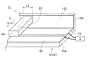
- FIG. 2 is a configuration diagram schematically illustrating a general electrostatic coupling type non-contact power feeding device 1Z.
- 2 is the moving direction F of the movable part 3 and the extending direction of the track member 151 on the fixed part 2 side.
- the front side surface of the track member 151 is omitted.
- the track member 151 is provided with two power supply electrodes 4X and 4Y.
- the two power supply electrodes 4X and 4Y are formed of a strip-shaped metal flat plate and have the same shape.
- the two power supply electrodes 4X and 4Y are disposed over the substantially entire length of the track member 151 (the total length in the left-right direction in FIG. 2) while being spaced apart on the bottom surface 15A of the track member 151.
- the high frequency power supply circuit 5 is disposed on the fixed portion 2 side. The high frequency power supply circuit 5 supplies high frequency power between the two power supply electrodes 4X and 4Y.
- the movable part 3 is provided with two power receiving electrodes 6X and 6Y.
- the two power receiving electrodes 6X and 6Y are formed of a strip-shaped metal flat plate and have the same shape.
- the two power receiving electrodes 6X and 6Y are disposed over substantially the entire length LZ of the movable portion 3, but are significantly shorter than the power feeding electrodes 4X and 4Y.
- the two power receiving electrodes 6X and 6Y are arranged in parallel and spaced apart from the power feeding electrodes 4X and 4Y on the fixed portion 2 side, respectively. As a result, capacitors are formed between the power supply electrodes 4X and 4Y and the power reception electrodes 6X and 6Y, respectively, and electrostatic contact type non-contact power supply is performed.
- the movable part 3 is equipped with a power receiving circuit and an electric load (not shown).
- the two power receiving electrodes 6X and 6Y are electrically connected to the input side of the power receiving circuit, and the output side of the power receiving circuit is electrically connected to the electric load.
- the power receiving circuit converts the high frequency power received by the power receiving electrodes 6X and 6Y and supplies the electric load to the electric load.
- a series resonant circuit is used to improve power supply capacity and power supply efficiency. That is, a resonance inductor is inserted and connected in the high frequency power supply circuit 5 or the power receiving circuit so that series resonance occurs at the output frequency of the high frequency power supply circuit 5.
- a coil is used as the resonance inductor.
- the resonance inductor is connected in series to a capacitor formed by the power feeding electrodes 4X and 4Y and the power receiving electrodes 6X and 6Y.
- the inductance value of the resonance inductor is determined so that the imaginary part of the impedance at the output frequency of the series resonance circuit is zero. Further, the output frequency of the high frequency power supply circuit 5 is also variably adjusted so as to match the resonance frequency.
- the feeding electrodes 4X and 4Y are divided into a plurality of divided electrodes, and abnormalities are detected early by comparing the divided currents with each other.
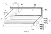
- FIG. 3 is a perspective view schematically showing a configuration of the electrostatic coupling type non-contact power feeding device 1 according to the first embodiment of the present invention.
- FIG. 4 is a functional configuration diagram of the electrostatic coupling type non-contact power feeding device 1 according to the first embodiment.
- the electrostatic coupling type non-contact power supply device 1 includes a pair of power supply electrodes 41 and 42, a high frequency power supply circuit 5, a pair of current detection comparison units 71 and 72, an abnormality determination unit 8, and a display unit 9 on the fixed unit 2 side. And a pair of power receiving electrodes 61 and 62, a power receiving circuit 65, an encoder 67 and the like are provided on the movable portion 3 side.
- the pair of power supply electrodes 41 and 42 includes three divided electrodes 411 to 413 and 421 to 423, respectively. Since the pair of power supply electrodes 41 and 42 have the same shape, one power supply electrode 41 will be described in detail below. As shown in FIG. 3, the three divided electrodes 411 to 413 constituting the power feeding electrode 41 are formed of a narrow metal plate and have a width dimension orthogonal to the moving direction of the movable portion 3. Are equal to each other. The three divided electrodes 411 to 413 extend in the moving direction F of the movable part 3 and are isolated and insulated from each other, and are arranged in parallel.
- the high frequency power supply circuit 5 is disposed on the fixed part 2 side. As shown in FIG. 4, one output terminal of the high frequency power supply circuit 5 is connected in parallel to the three divided electrodes 411 to 413 via the resonance coil 51. The other output terminal of the high-frequency power supply circuit 5 is connected in parallel to the three divided electrodes 421 to 423 via another resonance coil 52 having the same inductance value.
- the high frequency power supply circuit 5 supplies high frequency power in the 100 kHz to MHz band, for example.
- the output voltage and output frequency of the high-frequency power supply circuit 5 can be adjusted, and examples of the output voltage waveform include a sine wave and a rectangular wave.
- the pair of power receiving electrodes 61 and 62 on the movable part 3 side have the same shape as the electrodes 6X and 6Y shown in FIG.
- Each of the power receiving electrodes 61 and 62 is spaced apart from the three divided electrodes 411 to 413 and 421 to 423. Therefore, three capacitors are formed between the power receiving electrode 61 and the three divided electrodes 411 to 413, and three capacitors are also formed between the power receiving electrode 62 and the three divided electrodes 421 to 423. It is formed.
- the total capacitances C1 to C6 of the six capacitors are all equal to each other.
- a series resonance circuit is constituted by a total of six capacitors and two resonance coils 51 and 52.
- the current detection comparison units 71 and 72 are provided for the feeding electrodes 41 and 42 on the fixed unit 2 side, and have the same configuration. As shown in FIG. 4, one current detection / comparison unit 71 is disposed between the three divided electrodes 411 to 413 and the resonance coil 51. The current detection / comparison unit 71 detects and compares the current values I1, I2, and I3 of the currents flowing through the three divided electrodes 411 to 413, respectively.
- the other current detection / comparison unit 72 is disposed between the three divided electrodes 421 to 423 and the resonance coil 52.
- the current detection / comparison unit 72 detects and compares the current values I4, I5, and I6 of the currents flowing through the three divided electrodes 421 to 423, respectively.
- the three current values detected by the current detection comparison units 71 and 72 are equal to each other.
- the direction of the current is reversed in one current detection comparison unit 71 and the other current detection unit 72. That is, the following relationship is generally established between the current values I1 to I6. I1 ⁇ I2 ⁇ I3 ⁇ -I4 ⁇ -I5 ⁇ -I6
- a current transformer, a shunt resistor, a Hall element, or the like can be used as the current detection means of the current detection comparison units 71 and 72. Furthermore, as the current comparison means of the current detection comparison units 71 and 72, digital conversion of the current values I1 to I6 by the A / D converter, digital calculation by the CPU, and the like can be used. Each of the current detection comparison units 71 and 72 outputs the comparison result of the current values I1 to I6 to the abnormality determination unit 8.
- the abnormality determination unit 8 is provided on the fixed unit 2 side.
- the abnormality determination unit 8 determines the presence or absence of abnormality based on the comparison results of the current detection comparison units 71 and 72.
- the abnormality determination unit 8 outputs the determined result to the display unit 9 and presents it to the operator.
- the power receiving circuit 65 and the electric load 66 are mounted on the movable part 3.
- the power receiving electrodes 61 and 62 are electrically connected to the input terminal of the power receiving circuit 65.
- the output terminal of the power receiving circuit 65 is electrically connected to the electric load 66.
- the power receiving circuit 65 converts the high frequency power received by the power receiving electrodes 61 and 62 and supplies the electric load 66 with power.
- the power receiving circuit 65 is configured in accordance with the operating voltage specification of the electric load 66, and can be configured by, for example, a full-wave rectifier circuit or an inverter circuit.
- an encoder 67 for detecting the current position of the movable part 3 is provided on the movable part 3 side.
- the encoder 67 corresponds to a position detection unit of the present invention that detects the position of the movable unit 3 on the fixed unit 2.
- the position information detected by the encoder 67 is transmitted to the abnormality determination unit 8.
- the transmission form of the position information is not particularly limited, and wired communication or wireless communication can be used as appropriate.
- the encoder 67 and its position information may be shared not only by the abnormality determination unit 8 but also by a position control unit that controls the linear motor device 150.
- FIG. 5 is a diagram for explaining the normal operation and action in the first embodiment.
- FIG. 6 is a diagram for explaining the operation and action when the foreign substance BX is mixed between the electrodes in the first embodiment. 5 and 6 exemplify one power supply electrode 41, power reception electrode 61, and current detection comparison unit 71, and the other 42, 62, and 72 have the same operation and action.
- the abnormality determination unit 8 receives a comparison result indicating normality from both of the current detection comparison units 71 and 72 and performs a display corresponding to “normal” on the display unit 9.
- the foreign substance BX is mixed in the upper surface of the division
- the power receiving electrode 61 reaches above the foreign matter BX, the foreign matter BX is interposed between the electrodes of the capacitor formed between the divided electrode 413 and the power receiving electrode 61.
- the capacitance C3 changes, and the current flowing through the divided electrode 413 changes from the current value I3 to the current value I3X.
- the abnormality determination unit 8 determines that any one of the comparison results received from both the current detection comparison units 71 and 72 means abnormality, and determines that the display unit 9 displays a display corresponding to “abnormal”. Do. Furthermore, the abnormality determination unit 8 receives position information from the encoder 67 when an abnormality occurs, determines the location where the abnormality has occurred, and displays it on the display unit 9. In FIG. 6, the position where the power receiving electrode 61 is approaching the foreign substance BX is determined as the abnormality occurrence location. The operator can visually recognize the occurrence of an abnormality by visually checking the display unit 9 and can confirm the location of the abnormality. Therefore, the operator can easily find and remove the foreign matter BX, and return the apparatus 1 to the normal state.
- an abnormality other than the contamination of the foreign substance BX a local variation in the distance between the electrodes and peeling of the insulating layer on the electrode surface can be exemplified.
- These abnormalities can be caused by, for example, fatigue deformation due to repeated mechanical stress during use over time, or alteration or embrittlement of the insulating layer due to repeated thermal stress.
- the capacitances C1 to C6 both increase and decrease, and the current values I1 to I6 both increase and decrease. In the first embodiment, determination can be made regardless of the type of abnormality in which the current values I1 to I6 increase or decrease.
- the abnormality determination unit 8 easily determines the presence or absence of foreign matter and other abnormalities based on the comparison results of the current detection comparison units 71 and 72. it can. In particular, since it is not affected by the load fluctuation of the electric load 66 of the movable part 3, it is possible to detect an abnormality at a very early stage and improve the power supply reliability.
- the power feeding electrodes 41 and 42 are each composed of three divided electrodes 411 to 413 and 421 to 423 having the same width dimension. For this reason, the current values I1 to I3 and I4 to I6 of the currents flowing through the three divided electrodes 411 to 413 and 421 to 423 substantially coincide with each other regardless of the load variation, and the current values I1 to I3 only when an abnormality occurs. , I4 to I6 do not match. Therefore, the abnormality determination unit 8 can easily and accurately determine whether there is an abnormality.
- the abnormality determination unit 8 receives position information from the encoder 67 when an abnormality occurs, determines the location where the abnormality has occurred, and displays it on the display unit 9. Therefore, the operator can specify the location of the abnormality when the abnormality occurs, and can easily and efficiently perform maintenance such as inspection and maintenance.
- FIG. 7 is a diagram for partially explaining the configuration of the electrostatic coupling type non-contact power feeding device of the second embodiment.
- the configurations of the divided electrodes 431 to 433 constituting the feeding electrode 43 of the fixed portion are different.
- the power feeding electrode 43 includes three divided electrodes 431 to 433, and the shapes of the divided electrodes 431 to 433 are different from each other. That is, the width dimension of the centrally divided electrodes 432 that are separated and parallel to each other is approximately twice the width dimension of the divided electrodes 431 and 433 on both sides. Therefore, the capacitance C8 of the capacitor formed by the central divided electrode 432 and the power receiving electrode 61 is the capacitance C7 of the capacitor formed by the divided electrodes 431 and 433 and the power receiving electrode 61 on both sides. Approximately twice as large as C9. Further, the current values I7 to I9 of the currents flowing through the divided electrodes 431 to 433 are proportional to the capacitances C7 to C9.
- the ratio of the number of divided electrodes and the width dimension of the plurality of divided electrodes is not limited to the first and second embodiments, and can be appropriately designed. For example, when two divided electrodes having the same width dimension are used and the current values of the divided electrodes coincide with each other, it can be determined as normal. In this case, if the current values are different from each other, it can be determined that there is an abnormality, and it cannot be specified which of the divided electrodes is abnormal.
- the power feeding electrode (divided electrode) and the power receiving electrode are not limited to metal, and a plastic electrode formed of a conductive polymer or an electrode having a metal film formed on the surface of a resin core may be used. Good.
- the electrostatic coupling type non-contact power feeding device of the present invention is not limited to the board work equipment such as a component mounting machine, but has other movable industries that have a movable part and require non-contact power feeding. It can also be widely used for equipment. Further, it can be used for a non-contact power supply without using a pantograph or the like to a running train, or a non-contact power supply from a road surface to a running electric vehicle.
- Electrostatic coupling type non-contact power feeding device 2 Fixed part 3: Movable part 41, 42, 43, 4X, 4Y: Feeding electrode, 411 to 413, 421 to 423, 431 to 433: divided electrode 5: high frequency power supply circuit 51, 52: resonance coil 61, 62, 6X, 6Y: power receiving electrode 65: power receiving circuit 66: electric load 67: encoder (position Detection part) 71, 72, 73: Current detection comparison unit 8: Abnormality determination unit 9: Display unit 10: Component mounter 110: Board transport device 120: Component supply device 130, 140: Component transfer device 150: Linear motor device 151: Track Member 160: Movable main body 161: X-axis rail 170: Mounting head 190: Machine base
Landscapes
- Engineering & Computer Science (AREA)
- Computer Networks & Wireless Communication (AREA)
- Power Engineering (AREA)
- Manipulator (AREA)
- Measurement Of Length, Angles, Or The Like Using Electric Or Magnetic Means (AREA)
Abstract
本発明は、固定部に設けられた給電用電極と、固定部に移動可能に装架された可動部に設けられ、給電用電極に離隔対向して非接触で高周波電力を受け取る受電用電極と、受電用電極が受け取った高周波電力を変換して可動部上の電気負荷に給電する受電回路と、を備えた静電結合方式非接触給電装置であって、給電用電極は、可動部の移動方向に延在し相互に並べて配置された複数の分割電極からなり、各分割電極に流れる電流の電流値をそれぞれ検知して相互に比較する電流検知比較部と、電流検知比較部の比較結果に基づいて異常の有無を判定する異常判定部と、をさらに備えた。これにより、電極間への異物の混入などの異常を軽微な段階で早期に発見して給電信頼性を高めるとともに、異常発生箇所を特定してメンテナンスを容易にかつ効率的に行えるようにした。
Description
本発明は、可動部上の電気負荷に固定部から非接触で給電する非接触給電装置に関し、より詳細には、電極を離隔対向して配置した静電結合方式非接触給電装置に関する。
多数の部品が実装された基板を生産する基板用作業機器として、はんだ印刷機、部品実装機、リフロー機、基板検査機などがあり、これらを基板搬送装置で連結して基板生産ラインを構築する場合が多い。これらの基板用作業機器の多くは基板の上方を移動して所定の作業を行う可動部を備えており、可動部を駆動する一手段としてリニアモータ装置を用いることができる。リニアモータ装置は、移動方向に沿い複数の磁石のN極およびS極が交互に列設された軌道部材と、コアおよびコイルを有する電機子を含んで構成された可動部とを備えるのが一般的である。リニアモータ装置を始めとする可動部上の電気負荷に給電するために、従来から変形可能な給電用ケーブルが用いられてきた。また、近年では、給電用ケーブルによる荷搬重量の増加や金属疲労による断線のリスクなどの弊害を解消するために、非接触給電装置の適用が提案されている。
非接触給電装置の方式として、従来からコイルを用いた電磁誘導方式が多用されてきた。最近では、離隔対向する電極によりコンデンサを構成した静電結合方式も用いられるようになってきており、他に磁界共鳴方式なども検討されている。非接触給電装置の用途は、基板用作業機器に限定されるものではなく、他の業種の産業用機器や家電製品などの幅広い分野に広まりつつある。非接触給電装置では、離隔対向する給電用素子と受電用素子との間に異物が混入して給電性能が低下したり、故障したりするおそれが皆無でない。異物の混入などの異常に対する給電信頼性や安全性を高めた技術の一例が特許文献1に開示されている。
特許文献1の非接触による電力及び信号伝送装置は、給電発振部(高周波電源回路)および第1コイルを有する本体(固定部)と、第2コイルおよび定電圧部(受電回路)を有する端末(可動部)とから成り、端末に定電圧部の二次電圧および二次電流を検知する検知部を設け、検知した情報を信号伝達手段により本体に伝達して、給電発振部へ供給される一次電流が過電流であるか否かを判断するようにしている。これにより、第1コイルと第2コイルとの間に金属製異物がはさまって二次電圧が低下した場合などに、給電動作を停止して安全性を向上できる、と記載されている。
ところで、特許文献1の装置では、非接触給電装置に混入した金属製異物が異常発熱するなどの顕著な異常状態でないと異常の判断が難しい。例えば、電極を用いた静電結合方式非接触給電装置を基板用作業機器に搭載した場合、電気負荷の負荷状態が時々刻々と変化して、二次電圧、二次電流、および給電効率が変動する。このため、電極間に異物が混入したり電極に異常が発生したりして部分的に電流が集中しても、負荷変動と区別することが難しい。したがって、端末(可動部)側で二次電圧および二次電流を検知して、本体(固定部)側の一次電流と比較照合しても、軽微な異常を判断することは困難である。軽微な異常を放置して静電結合方式非接触給電装置を使用し続けると、局部的に電極表面の絶縁層が劣化したり電極面が荒れたりして異常が進展し、最終的には絶縁破壊が発生して給電できなくなる。
また、非接触給電装置は、基板用作業機器に例示されるように固定部から可動部への非接触給電の用途に適用される場合が多い。このため、軽微な異常を検出しても異常発生箇所を特定できないと、メンテナンスが困難あるいは非効率になるおそれがある。
本発明は、上記背景技術の問題点に鑑みてなされたもので、電極間への異物の混入などの異常を軽微な段階で早期に発見して給電信頼性を高めるとともに、異常発生箇所を特定してメンテナンスを容易にかつ効率的に行えるようにした静電結合方式非接触給電装置を提供することを解決すべき課題とする。
上記課題を解決する請求項1に係る静電結合方式非接触給電装置の発明は、固定部に設けられた給電用電極と、前記給電用電極に高周波電力を給電する高周波電源回路と、前記固定部に移動可能に装架された可動部に設けられ、前記給電用電極に離隔対向して非接触で高周波電力を受け取る受電用電極と、前記受電用電極が受け取った高周波電力を変換して前記可動部上の電気負荷に給電する受電回路と、を備えた静電結合方式非接触給電装置であって、前記給電用電極は、前記可動部の移動方向に延在し相互に並べて配置された複数の分割電極からなり、各前記分割電極に流れる電流の電流値をそれぞれ検知して相互に比較する電流検知比較部と、前記電流検知比較部の比較結果に基づいて異常の有無を判定する異常判定部と、をさらに備えた。
請求項2に係る発明は、請求項1において、前記複数の分割電極は相互に平行配置されている。
請求項3に係る発明は、請求項2において、前記給電用電極は、前記可動部の移動方向と直交する幅寸法が互いに等しい少なくとも3個の分割電極からなり、前記異常判定部は、前記電流検知比較部で検知された各前記分割電極に流れる電流の電流値が相互に概ね一致しているときに異常無しと判定し、一致していないときに異常有りと判定する。
請求項4に係る発明は、請求項1~3のいずれか一項において、前記異常判定部は、前記固定部上における前記可動部の位置を検知する位置検知部から前記可動部の位置情報を受け取り、前記電流検知比較部の比較結果に基づいて異常有りと判定したときに、前記位置情報に基づいて異常発生箇所を併せて判定する。
請求項1に係る静電結合方式非接触給電装置の発明では、給電用電極が複数の分割電極からなるので、各分割電極と受電用電極との間にそれぞれコンデンサが形成される。そして、高周波電源回路から各コンデンサに電流が分流して可動部への給電が行われる。ここで、いずれかの分割電極と受電用電極との間に異物が混入したときには、当該のコンデンサの静電容量のみが変化して当該の電流値のみが著変する。一方、可動部の電気負荷で負荷変動が発生したときには、各分割電極に流れる電流が揃って変化する。したがって、電流検知比較部で各分割電極に流れる電流の電流値をそれぞれ検知して相互に比較してやれば、その比較結果に基づいて異常判定部は異物の混入の有無を容易に判定できる。また、異物の混入以外の原因で静電容量が変化する異常、例えば、局部的な電極間距離の変動や電極表面の絶縁層の剥離などの異常も同様に判定できる。本発明によれば、負荷変動の影響を受けないので、異常を軽微な段階で早期に発見して給電信頼性を高めることができる。
請求項2に係る発明では、複数の分割電極は相互に平行配置されているので、可動部が移動しても、その影響を受けずに異常の有無を判定できる。
請求項3に係る発明では、給電用電極は幅寸法が互いに等しい少なくとも3個の分割電極からなるので、各分割電極と受電用電極との間に形成される少なくとも3個のコンデンサの静電容量が互いに等しくなる。このため、負荷変動に関わらず各分割電極に流れる電流の電流値は略一致し、異常が発生したときだけ電流値が一致しなくなる。したがって、異常判定部は、異常の有無を容易にかつ高精度に判定できる。
請求項4に係る発明では、異常判定部は、位置検知部から可動部の位置情報を受け取り、異常有りと判定したときに位置情報に基づいて異常発生箇所を併せて判定する。したがって、オペレータは、異常発生時に異常発生箇所を特定でき、点検や手入れなどのメンテナンスを容易にかつ効率的に行える。
まず、本発明を適用できる部品実装機10について、図1を参考にして説明する。図1は、本発明の第1実施形態の静電結合方式非接触給電装置1を適用できる部品実装機10の全体構成を示した斜視図である。部品実装機10は、基板に多数の部品を実装する装置であり、2セットの同一構造の部品実装ユニットが概ね左右対称に配置されて構成されている。ここでは、図1の右手前側のカバーを取り外した状態の部品実装ユニットを例にして説明する。なお、図中の左奥側から右手前側に向かう部品実装機10の幅方向をX軸方向とし、部品実装機10の長手方向をY軸方向とする。
部品実装機10は、基板搬送装置110、部品供給装置120、2つの部品移載装置130、140などが機台190に組み付けられて構成されている。基板搬送装置110は、部品実装機10の長手方向の中央付近をX軸方向に横断するように配設されている。基板搬送装置110は、図略の搬送コンベアを有しており、基板をX軸方向に搬送する。また、基板搬送装置110は、図略のクランプ装置を有しており、基板を所定の実装作業位置に固定および保持する。部品供給装置120は、部品実装機10の長手方向の前部(図1の左前側)及び後部(図には見えない)に設けられている。部品供給装置120は、複数のカセット式フィーダ121を有し、各フィーダ121にセットされたキャリアテープから2つの部品移載装置130、140に連続的に部品を供給するようになっている。
2つの部品移載装置130、140は、X軸方向およびY軸方向に移動可能ないわゆるXYロボットタイプの装置である。2つの部品移載装置130、140は、部品実装機10の長手方向の前側および後側に、相互に対向するように配設されている。各部品移載装置130、140は、Y軸方向の移動のためのリニアモータ装置150を有している。
リニアモータ装置150は、2つの部品移載装置130、140に共通な軌道部材151および補助レール155と、2つの部品移載装置130、140ごとのリニア可動部153で構成されている。軌道部材151は、本発明の固定部2の一部に相当し、リニア可動部153の移動方向となるY軸方向に延在している。軌道部材151は、リニア可動部153の下側に配置された底面15A、およびリニア可動部153の両側に配置された側面15Bからなり、上方に開口する溝形状になっている。軌道部材151の向かい合う側面15Bの内側には、Y軸方向に沿って複数の磁石152が列設されている。
リニア可動部153は、軌道部材151に移動可能に装架されている。リニア可動部153は、本発明の可動部3に相当し、可動本体部160、X軸レール161、および実装ヘッド170などで構成されている。可動本体部160は、Y軸方向に延在しており、その両側面には軌道部材151の磁石152に対向して推進力を発生する電機子が配設されている。X軸レール161は、可動本体部160からX軸方向に延在している。X軸レール161は、一端162が可動本体部160に結合され、他端163が補助レール155に移動可能に装架されており、可動本体部160と一体的にY軸方向に移動するようになっている。
部品実装ヘッド170は、X軸レール161に装架され、X軸方向に移動するようになっている。部品実装ヘッド170の下端には図略の吸着ノズルが設けられている。吸着ノズルは、負圧を利用して部品供給装置120から部品を吸着採取し、実装作業位置の基板に実装する。X軸レール161上に設けられた図略のボールねじ送り機構は、ボールねじを回転駆動するX軸モータを有しており、部品実装ヘッド170をX軸方向に駆動する。部品実装ヘッド170を動作させるためにリニア可動部153(可動部3)に装備された複数の電装品は、本発明の電気負荷に相当する。なお、リニアモータ装置150の電機子も電気負荷に含まれている。
部品実装機10は、他に、オペレータと情報を交換するための表示設定装置180および、基板や部品を撮像する図略のカメラなどを備えている。
次に、一般的な静電結合方式非接触給電装置1Zについて、図2を参考にして説明する。図2は、一般的な静電結合方式非接触給電装置1Zを模式的に説明する構成図である。図2の左右方向が可動部3の移動方向Fであり、かつ、固定部2側の軌道部材151の延在方向である。また、図2で、軌道部材151の手前側の側面は省略されている。図示されるように、軌道部材151には、2個の給電用電極4X、4Yが配設されている。2個の給電用電極4X、4Yは、帯状の金属製平板で形成されており、かつ互いに同じ形状である。2個の給電用電極4X、4Yは、軌道部材151の底面15A上に離隔しつつ軌道部材151の概ね全長(図2の左右方向の全長)にわたって配設されている。高周波電源回路5は、固定部2側に配設されている。高周波電源回路5は、高周波電力を2個の給電用電極4X、4Yの間に給電する。
また、可動部3には、2個の受電用電極6X、6Yが設けられている。2個の受電用電極6X、6Yは、帯状の金属製平板で形成されており、かつ互いに同じ形状である。2個の受電用電極6X、6Yは、可動部3の概ね全長LZにわたって配設されているが、給電用電極4X、4Yよりも格段に短い。2個の受電用電極6X、6Yは、それぞれ、固定部2側の給電用電極4X、4Yに離隔対向して平行配置される。これにより、給電用電極4X、4Yと受電用電極6X、6Yとの間にそれぞれコンデンサが形成され、静電結合方式の非接触給電が行われる。
また、可動部3には、図略の受電回路および電気負荷が搭載されている。2個の受電用電極6X、6Yは、受電回路の入力側に電気接続され、受電回路の出力側は電気負荷に電気接続されている。受電回路は、受電用電極6X、6Yが受け取った高周波電力を変換して、電気負荷に給電する。
また通常、給電容量および給電効率の向上を図るために、直列共振回路が用いられる。つまり、高周波電源回路5の出力周波数で直列共振が発生するように、高周波電源回路5内または受電回路内に共振用インダクタが挿入接続される。共振用インダクタとして、一般的にはコイルを用いる。共振用インダクタは、給電用電極4X、4Yと受電用電極6X、6Yとで形成されるコンデンサに対して直列接続される。共振用インダクタのインダクタンス値は、直列共振回路の出力周波数におけるインピーダンスの虚数部がゼロになるように定められている。さらに、高周波電源回路5の出力周波数も、共振周波数に一致するように可変に調整される。
一般的な静電結合方式非接触給電装置1Zにおいて、例えば、給電用電極4Xと受電用電極6Xとの間に異物が混入すると、コンデンサの静電容量が変化して、流れる電流が変化する。しかしながら、この電流変化は、可動部3に搭載された電気負荷の負荷変動と区別することが難しい。したがって、従来技術で、異物の混入の異常を早期に検出することは困難である。そこで、本発明では、給電用電極4X、4Yを複数の分割電極に分割し、分流する電流を相互に比較することで異常を早期に検出する。
図3は、本発明の第1実施形態の静電結合方式非接触給電装置1の構成を模式的に示す斜視図である。また、図4は、第1実施形態の静電結合方式非接触給電装置1の機能構成図である。静電結合方式非接触給電装置1は、固定部2側に一対の給電用電極41、42、高周波電源回路5、一対の電流検知比較部71、72、異常判定部8、および表示部9などを備え、可動部3側に一対の受電用電極61、62、受電回路65、エンコーダ67などを備えて構成されている。
一対の給電用電極41、42はそれぞれ、3個の分割電極411~413、421~423からなっている。一対の給電用電極41、42は互いに同じ形状であるので、以下では一方の給電用電極41について詳述する。図3に示されるように、給電用電極41を構成する3個の分割電極411~413は、細帯状の金属製平板で形成されており、かつ可動部3の移動方向と直交する幅寸法が互いに等しくなっている。3個の分割電極411~413は、可動部3の移動方向Fに延在して相互に離隔絶縁され、平行配置されている。
高周波電源回路5は、固定部2側に配設されている。図4に示されるように、高周波電源回路5の一方の出力端子は、共振用コイル51を経由して3個の分割電極411~413に並列接続されている。高周波電源回路5の他方の出力端子は、同じインダクタンス値を有する別の共振用コイル52を経由して3個の分割電極421~423に並列接続されている。高周波電源回路5は、例えば、100kHz~MHz帯の高周波電力を給電する。高周波電源回路5の出力電圧および出力周波数は調整可能とされており、出力電圧波形として正弦波や矩形波などを例示できる。
一方、可動部3側の一対の受電用電極61、62は、図2に示された電極6X、6Yと同じ形状である。受電用電極61、62はそれぞれ、3個の分割電極411~413,421~423と離隔対向配置されている。したがって、受電用電極61と3個の分割電極411~413との間に3個のコンデンサが形成され、受電用電極62と3個の分割電極421~423との間にも3個のコンデンサが形成される。合計6個のコンデンサの静電容量C1~C6は、全て互いに等しくなる。また、合計6個のコンデンサと2個の共振用コイル51、52とにより直列共振回路が構成される。
電流検知比較部71、72は、固定部2側の給電用電極41、42に対してそれぞれ設けられており、互いに同じ構成である。図4に示されるように、一方の電流検知比較部71は、3個の分割電極411~413と共振用コイル51との間に配設されている。電流検知比較部71は、3個の分割電極411~413にそれぞれ流れる電流の電流値I1、I2、I3を検知して相互に比較する。
同様に、他方の電流検知比較部72は、3個の分割電極421~423と共振用コイル52との間に配設されている。電流検知比較部72は、3個の分割電極421~423にそれぞれ流れる電流の電流値I4、I5、I6を検知して相互に比較する。装置1が良好に給電動作を行っているとき、各電流検知比較部71、72が検知する3つの電流値は互いに等しくなっている。また、一方の電流検知比較部71と他方の電流検知部72とでは、電流の向きは逆になっている。つまり、各電流値I1~I6には概ね次の関係が成り立つ。
I1≒I2≒I3≒-I4≒-I5≒-I6
I1≒I2≒I3≒-I4≒-I5≒-I6
電流検知比較部71、72の電流検知手段として、変流器、シャント抵抗、ホール素子などを用いることができる。さらに、電流検知比較部71、72の電流比較手段として、A/D変換器による電流値I1~I6のディジタル変換、およびCPUによるディジタル演算などを用いることができる。各電流検知比較部71、72は、電流値I1~I6の比較結果を異常判定部8に出力する。
異常判定部8は、固定部2側に設けられている。異常判定部8は、電流検知比較部71、72の比較結果に基づいて異常の有無を判定する。異常判定部8は、判定した結果を表示部9に出力して、オペレータに提示する。
可動部3には、受電回路65および電気負荷66が搭載されている。受電用電極61、62は、受電回路65の入力端子に電気接続されている。受電回路65の出力端子は、電気負荷66に電気接続されている。受電回路65は、受電用電極61、62が受け取った高周波電力を変換して、電気負荷66に給電する。受電回路65は、電気負荷66の動作電圧仕様に合わせて回路構成されており、例えば、全波整流回路やインバータ回路などで構成できる。
また、可動部3側には、可動部3の現在位置を検知するエンコーダ67が設けられている。エンコーダ67は、固定部2上における可動部3の位置を検知する本発明の位置検知部に相当する。エンコーダ67が検知した位置情報は、異常判定部8に伝送されるようになっている。位置情報の伝送形態は特に制約されず、有線通信や無線通信などを適宜使用できる。なお、エンコーダ67およびその位置情報は、異常判定部8だけでなく、リニアモータ装置150の制御を行う位置制御部に共用されてもよい。
次に、上述のように構成された第1実施形態の静電結合方式非接触給電装置1の動作および作用について説明する。図5は、第1実施形態における正常時の動作および作用を説明する図である。また、図6は、第1実施形態における電極間への異物BX混入時の動作および作用を説明する図である。図5および図6では、一方の給電用電極41、受電用電極61、および電流検知比較部71を例示しており、他方42、62,72でも動作および作用は同様である。
図5で、非接触給電装置1が正常に動作していると、白抜き矢印Fで示されるように可動部2の受電用電極61が移動しても、3個の分割電極41と受電用電極61との離隔距離が一定に保たれる。したがって、3個の静電容量C1~C3が一定で互いに等しく保たれ、3個の電流値I1~I3も互いに等しくなる(I1=I2=I3)。このとき、可動部3の電気負荷66で負荷変動が発生すると、電流値I1~I3の大きさは変化するが、互いに等しいことに変わりはない。したがって、これを検知した電流検知比較部71は、正常を意味する「I1=I2=I3」の比較結果を異常判定部8に出力する。異常判定部8は、両方の電流検知比較部71、72から正常を意味する比較結果を受け取り、表示部9で「正常」に相当する表示を行う。
これに対して、図6では、図中の奥側の分割電極413の上面に異物BXが混入している。可動部2が移動しても、受電用電極61が異物BXから離れている間は、3個の電流値I1~I3は互いに等しい(I1=I2=I3)。受電用電極61が異物BXの上方にさしかかると、分割電極413と受電用電極61との間に形成されるコンデンサの電極間に異物BXが介在する。これにより、静電容量C3が変化して、分割電極413に流れる電流が電流値I3から電流値I3Xに変化する。また、他の分割電極411、412の静電容量C1、C2や電流値I1、I2は著変しない。つまり、電流値I3Xは、電流値I1、I2とは異なる。したがって、これを検知した電流検知比較部71は、異常を意味する「I1=I2≠I3」の比較結果を異常判定部8に出力する。
異常判定部8は、両方の電流検知比較部71、72から受け取った比較結果のうち一方でも異常を意味するものがあれば異常と判定して、表示部9で「異常」に相当する表示を行う。さらに、異常判定部8は、異常が発生したときにエンコーダ67から位置情報を受け取って異常発生個所を判定し、表示部9で表示する。図6では、受電用電極61が異物BXの上方にさしかかった位置を異常発生個所と判定する。オペレータは、表示部9を視認することで異常の発生を知り、異常発生個所を確認できる。したがって、オペレータは、容易に異物BXを見つけて除去し、装置1を正常状態に復帰できる。
また、異物BXの混入以外の異常として、局部的な電極間距離の変動、および電極表面の絶縁層の剥離を例示できる。これらの異常は、例えば、経年使用時の機械的なストレスの繰り返しによる疲労変形や、熱的なストレスの繰り返しによる絶縁層の変質や脆化などによって生じ得る。いろいろな異常の種類を考慮すると、静電容量C1~C6の増加と減少の両方の場合が考えられ、電流値I1~I6も増加と減少の両方の場合が考えられる。本第1実施形態では、電流値I1~I6が増加または減少する異常の種類を問わずに判定できる。
第1実施形態の静電結合方式非接触給電装置1では、電流検知比較部71、72の比較結果に基づいて異常判定部8は、異物の混入の有無やその他に起因する異常を容易に判定できる。特に、可動部3の電気負荷66の負荷変動の影響を受けないので、異常を軽微な段階で早期に発見して給電信頼性を高めることができる。
また給電用電極41、42はそれぞれ、幅寸法が互いに等しい3個の分割電極411~413、421~423からなっている。このため、負荷変動に関わらず3個の分割電極411~413、421~423に流れる電流の電流値I1~I3、I4~I6は互いに略一致し、異常が発生したときだけ電流値I1~I3、I4~I6が一致しなくなる。したがって、異常判定部8は、異常の有無を容易にかつ高精度に判定できる。
さらに、異常判定部8は、異常が発生したときにエンコーダ67から位置情報を受け取って異常発生個所を判定し、表示部9で表示する。したがって、オペレータは、異常発生時に異常発生箇所を特定でき、点検や手入れなどのメンテナンスを容易にかつ効率的に行える。
次に、第2実施形態の静電結合方式非接触給電装置について、第1実施形態と異なる点を主に説明する。図7は、第2実施形態の静電結合方式非接触給電装置の構成を部分的に説明する図である。第2実施形態では、固定部の給電用電極43を構成する分割電極431~433の構成が異なっている。
図7に示されるように、給電用電極43は3個の分割電極431~433からなり、分割電極431~433の形状が互いに異なっている。すなわち、離隔平行する中央の分割電極432の幅寸法は、両側の分割電極431、433の幅寸法の略2倍になっている。このため、中央の分割電極432と受電用電極61とで形成されるコンデンサの静電容量C8は、両側の分割電極431、433と受電用電極61とで形成されるコンデンサの静電容量C7、C9の略2倍になる。また、各分割電極431~433に流れる電流の電流値I7~I9は、静電容量C7~C9に比例する。
したがって、電流検知比較部73は、各電流値I7~I9を検知し、両側の電流値I7、I9を2倍して中央の電流値I8と比較する。つまり、異常判定部8は、次式が成立しているときに正常と判定し、成立していないときに異常と判定する。
2×I7=I8=2×I9
2×I7=I8=2×I9
第2実施形態における動作、作用、および効果は、第1実施形態と同様であるので、説明は省略する。
なお、複数の分割電極の分割数や幅寸法の比は、第1および第2実施形態に限定されず、適宜設計できる。例えば、幅寸法が互いに等しい2個の分割電極を用い、各分割電極の電流値が互いに一致しているときに正常と判定することができる。この場合、電流値が互いに異なれば異常と判定でき、どちらの分割電極に異常が発生しているかまでは特定できない。また、給電用電極(分割電極)や受電用電極は金属製に限定されず、導電性高分子で形成されたプラスチック電極や樹脂製芯体の表面に金属皮膜を形成した電極などを用いてもよい。さらに、給電用電極を分割せずに受電用電極を分割して、可動部側に電流検知比較部を設ける別法も技術的には可能である。しかしながら、この別法では、可動部の構成部品点数が増加して重量化し、可動部側の消費電力も増加するので、必ずしも賢明とは言えない。本発明は、その他にも様々な変形や応用が可能である。
本発明の静電結合方式非接触給電装置は、部品実装機を始めとする基板用作業機器に限定されるものでなく、可動部を有して非接触給電を必要とする他の業種の産業用機器にも広く利用できる。さらには、走行中の電車に対してパンタグラフなどを用いずに非接触給電する用途や、走行中の電気自動車に対して路面から非接触給電する用途などにも利用可能である。
1、1Z:静電結合方式非接触給電装置
2:固定部 3:可動部
41、42、43、4X、4Y:給電用電極、
411~413、421~423、431~433:分割電極
5:高周波電源回路 51、52:共振用コイル
61、62、6X、6Y:受電用電極
65:受電回路 66:電気負荷
67:エンコーダ(位置検知部)
71、72、73:電流検知比較部
8:異常判定部
9:表示部
10:部品実装機
110:基板搬送装置 120:部品供給装置
130、140:部品移載装置
150:リニアモータ装置 151:軌道部材
160:可動本体部 161:X軸レール
170:実装ヘッド 190:機台
2:固定部 3:可動部
41、42、43、4X、4Y:給電用電極、
411~413、421~423、431~433:分割電極
5:高周波電源回路 51、52:共振用コイル
61、62、6X、6Y:受電用電極
65:受電回路 66:電気負荷
67:エンコーダ(位置検知部)
71、72、73:電流検知比較部
8:異常判定部
9:表示部
10:部品実装機
110:基板搬送装置 120:部品供給装置
130、140:部品移載装置
150:リニアモータ装置 151:軌道部材
160:可動本体部 161:X軸レール
170:実装ヘッド 190:機台
Claims (4)
- 固定部に設けられた給電用電極と、
前記給電用電極に高周波電力を給電する高周波電源回路と、
前記固定部に移動可能に装架された可動部に設けられ、前記給電用電極に離隔対向して非接触で高周波電力を受け取る受電用電極と、
前記受電用電極が受け取った高周波電力を変換して前記可動部上の電気負荷に給電する受電回路と、を備えた静電結合方式非接触給電装置であって、
前記給電用電極は、前記可動部の移動方向に延在し相互に並べて配置された複数の分割電極からなり、
各前記分割電極に流れる電流の電流値をそれぞれ検知して相互に比較する電流検知比較部と、
前記電流検知比較部の比較結果に基づいて異常の有無を判定する異常判定部と、をさらに備えた静電結合方式非接触給電装置。 - 請求項1において、前記複数の分割電極は相互に平行配置されている静電結合方式非接触給電装置。
- 請求項2において、
前記給電用電極は、前記可動部の移動方向と直交する幅寸法が互いに等しい少なくとも3個の分割電極からなり、
前記異常判定部は、前記電流検知比較部で検知された各前記分割電極に流れる電流の電流値が相互に概ね一致しているときに異常無しと判定し、一致していないときに異常有りと判定する静電結合方式非接触給電装置。 - 請求項1~3のいずれか一項において、
前記異常判定部は、前記固定部上における前記可動部の位置を検知する位置検知部から前記可動部の位置情報を受け取り、前記電流検知比較部の比較結果に基づいて異常有りと判定したときに、前記位置情報に基づいて異常発生箇所を併せて判定する静電結合方式非接触給電装置。
Priority Applications (2)
| Application Number | Priority Date | Filing Date | Title |
|---|---|---|---|
| PCT/JP2012/082242 WO2014091584A1 (ja) | 2012-12-12 | 2012-12-12 | 静電結合方式非接触給電装置 |
| JP2014551790A JP6086927B2 (ja) | 2012-12-12 | 2012-12-12 | 静電結合方式非接触給電装置 |
Applications Claiming Priority (1)
| Application Number | Priority Date | Filing Date | Title |
|---|---|---|---|
| PCT/JP2012/082242 WO2014091584A1 (ja) | 2012-12-12 | 2012-12-12 | 静電結合方式非接触給電装置 |
Publications (1)
| Publication Number | Publication Date |
|---|---|
| WO2014091584A1 true WO2014091584A1 (ja) | 2014-06-19 |
Family
ID=50933906
Family Applications (1)
| Application Number | Title | Priority Date | Filing Date |
|---|---|---|---|
| PCT/JP2012/082242 Ceased WO2014091584A1 (ja) | 2012-12-12 | 2012-12-12 | 静電結合方式非接触給電装置 |
Country Status (2)
| Country | Link |
|---|---|
| JP (1) | JP6086927B2 (ja) |
| WO (1) | WO2014091584A1 (ja) |
Cited By (2)
| Publication number | Priority date | Publication date | Assignee | Title |
|---|---|---|---|---|
| WO2020213308A1 (ja) * | 2019-04-19 | 2020-10-22 | 株式会社デンソー | 走行中給電システム及びその電気特性の異常値判定方法 |
| WO2021018641A1 (de) * | 2019-07-29 | 2021-02-04 | Bayerische Motoren Werke Aktiengesellschaft | Energieübertragungsvorrichtung zum drahtlosen übertragen von elektrischer energie, sowie verfahren |
Citations (3)
| Publication number | Priority date | Publication date | Assignee | Title |
|---|---|---|---|---|
| JP2012090374A (ja) * | 2010-10-15 | 2012-05-10 | Sony Corp | 電子機器、給電方法および給電システム |
| WO2012070479A1 (ja) * | 2010-11-25 | 2012-05-31 | 株式会社村田製作所 | 電力伝送システム、及び該電力伝送システムで用いる送電装置 |
| JP2012213270A (ja) * | 2011-03-31 | 2012-11-01 | Panasonic Corp | 非接触給電システム |
-
2012
- 2012-12-12 JP JP2014551790A patent/JP6086927B2/ja not_active Expired - Fee Related
- 2012-12-12 WO PCT/JP2012/082242 patent/WO2014091584A1/ja not_active Ceased
Patent Citations (3)
| Publication number | Priority date | Publication date | Assignee | Title |
|---|---|---|---|---|
| JP2012090374A (ja) * | 2010-10-15 | 2012-05-10 | Sony Corp | 電子機器、給電方法および給電システム |
| WO2012070479A1 (ja) * | 2010-11-25 | 2012-05-31 | 株式会社村田製作所 | 電力伝送システム、及び該電力伝送システムで用いる送電装置 |
| JP2012213270A (ja) * | 2011-03-31 | 2012-11-01 | Panasonic Corp | 非接触給電システム |
Cited By (5)
| Publication number | Priority date | Publication date | Assignee | Title |
|---|---|---|---|---|
| WO2020213308A1 (ja) * | 2019-04-19 | 2020-10-22 | 株式会社デンソー | 走行中給電システム及びその電気特性の異常値判定方法 |
| JP2020178471A (ja) * | 2019-04-19 | 2020-10-29 | 株式会社デンソー | 走行中給電システム及びその電気特性の異常値判定方法 |
| JP7167829B2 (ja) | 2019-04-19 | 2022-11-09 | 株式会社デンソー | 走行中給電システム及びその電気特性の異常値判定方法 |
| WO2021018641A1 (de) * | 2019-07-29 | 2021-02-04 | Bayerische Motoren Werke Aktiengesellschaft | Energieübertragungsvorrichtung zum drahtlosen übertragen von elektrischer energie, sowie verfahren |
| US11858435B2 (en) | 2019-07-29 | 2024-01-02 | Bayerische Motoren Werke Aktiengesellschaft | Energy transmission device for wirelessly transmitting electric energy, and method |
Also Published As
| Publication number | Publication date |
|---|---|
| JP6086927B2 (ja) | 2017-03-01 |
| JPWO2014091584A1 (ja) | 2017-01-05 |
Similar Documents
| Publication | Publication Date | Title |
|---|---|---|
| JP6049742B2 (ja) | 静電結合方式非接触給電装置 | |
| WO2014006685A1 (ja) | 静電結合方式非接触給電装置 | |
| CN104604090B (zh) | 非接触供电装置 | |
| JP6161683B2 (ja) | 静電結合方式非接触給電装置 | |
| CN104704707B (zh) | 非接触供电装置 | |
| JP6086927B2 (ja) | 静電結合方式非接触給電装置 | |
| JP6170057B2 (ja) | 静電結合方式非接触給電装置およびその制御方法 | |
| CN108604822B (zh) | 非接触供电装置 | |
| JP6343003B2 (ja) | 非接触給電装置 | |
| JP6678730B2 (ja) | 非接触給電装置 | |
| JP6049743B2 (ja) | 静電結合方式非接触給電装置 | |
| JP6058003B2 (ja) | 静電結合方式非接触給電装置 | |
| JP6104231B2 (ja) | 静電結合方式非接触給電装置 | |
| JP2018133930A (ja) | 非接触送電装置、非接触受電装置、および非接触給電システム | |
| WO2016016930A1 (ja) | 非接触給電装置 |
Legal Events
| Date | Code | Title | Description |
|---|---|---|---|
| 121 | Ep: the epo has been informed by wipo that ep was designated in this application |
Ref document number: 12889868 Country of ref document: EP Kind code of ref document: A1 |
|
| ENP | Entry into the national phase |
Ref document number: 2014551790 Country of ref document: JP Kind code of ref document: A |
|
| NENP | Non-entry into the national phase |
Ref country code: DE |
|
| 122 | Ep: pct application non-entry in european phase |
Ref document number: 12889868 Country of ref document: EP Kind code of ref document: A1 |