WO2014088086A1 - 表示装置 - Google Patents
表示装置 Download PDFInfo
- Publication number
- WO2014088086A1 WO2014088086A1 PCT/JP2013/082766 JP2013082766W WO2014088086A1 WO 2014088086 A1 WO2014088086 A1 WO 2014088086A1 JP 2013082766 W JP2013082766 W JP 2013082766W WO 2014088086 A1 WO2014088086 A1 WO 2014088086A1
- Authority
- WO
- WIPO (PCT)
- Prior art keywords
- display device
- light
- optical film
- anisotropic optical
- color change
- Prior art date
- Legal status (The legal status is an assumption and is not a legal conclusion. Google has not performed a legal analysis and makes no representation as to the accuracy of the status listed.)
- Ceased
Links
Images


Classifications
-
- G—PHYSICS
- G02—OPTICS
- G02B—OPTICAL ELEMENTS, SYSTEMS OR APPARATUS
- G02B5/00—Optical elements other than lenses
- G02B5/02—Diffusing elements; Afocal elements
- G02B5/0205—Diffusing elements; Afocal elements characterised by the diffusing properties
- G02B5/0236—Diffusing elements; Afocal elements characterised by the diffusing properties the diffusion taking place within the volume of the element
- G02B5/0242—Diffusing elements; Afocal elements characterised by the diffusing properties the diffusion taking place within the volume of the element by means of dispersed particles
-
- G—PHYSICS
- G02—OPTICS
- G02B—OPTICAL ELEMENTS, SYSTEMS OR APPARATUS
- G02B5/00—Optical elements other than lenses
- G02B5/02—Diffusing elements; Afocal elements
- G02B5/0205—Diffusing elements; Afocal elements characterised by the diffusing properties
- G02B5/0257—Diffusing elements; Afocal elements characterised by the diffusing properties creating an anisotropic diffusion characteristic, i.e. distributing output differently in two perpendicular axes
-
- G—PHYSICS
- G02—OPTICS
- G02B—OPTICAL ELEMENTS, SYSTEMS OR APPARATUS
- G02B5/00—Optical elements other than lenses
- G02B5/02—Diffusing elements; Afocal elements
- G02B5/0205—Diffusing elements; Afocal elements characterised by the diffusing properties
- G02B5/0263—Diffusing elements; Afocal elements characterised by the diffusing properties with positional variation of the diffusing properties, e.g. gradient or patterned diffuser
-
- G—PHYSICS
- G02—OPTICS
- G02B—OPTICAL ELEMENTS, SYSTEMS OR APPARATUS
- G02B5/00—Optical elements other than lenses
- G02B5/02—Diffusing elements; Afocal elements
- G02B5/0273—Diffusing elements; Afocal elements characterized by the use
- G02B5/0278—Diffusing elements; Afocal elements characterized by the use used in transmission
-
- G—PHYSICS
- G02—OPTICS
- G02F—OPTICAL DEVICES OR ARRANGEMENTS FOR THE CONTROL OF LIGHT BY MODIFICATION OF THE OPTICAL PROPERTIES OF THE MEDIA OF THE ELEMENTS INVOLVED THEREIN; NON-LINEAR OPTICS; FREQUENCY-CHANGING OF LIGHT; OPTICAL LOGIC ELEMENTS; OPTICAL ANALOGUE/DIGITAL CONVERTERS
- G02F1/00—Devices or arrangements for the control of the intensity, colour, phase, polarisation or direction of light arriving from an independent light source, e.g. switching, gating or modulating; Non-linear optics
- G02F1/01—Devices or arrangements for the control of the intensity, colour, phase, polarisation or direction of light arriving from an independent light source, e.g. switching, gating or modulating; Non-linear optics for the control of the intensity, phase, polarisation or colour
- G02F1/13—Devices or arrangements for the control of the intensity, colour, phase, polarisation or direction of light arriving from an independent light source, e.g. switching, gating or modulating; Non-linear optics for the control of the intensity, phase, polarisation or colour based on liquid crystals, e.g. single liquid crystal display cells
- G02F1/133—Constructional arrangements; Operation of liquid crystal cells; Circuit arrangements
- G02F1/1333—Constructional arrangements; Manufacturing methods
- G02F1/1335—Structural association of cells with optical devices, e.g. polarisers or reflectors
- G02F1/133504—Diffusing, scattering, diffracting elements
-
- G—PHYSICS
- G02—OPTICS
- G02F—OPTICAL DEVICES OR ARRANGEMENTS FOR THE CONTROL OF LIGHT BY MODIFICATION OF THE OPTICAL PROPERTIES OF THE MEDIA OF THE ELEMENTS INVOLVED THEREIN; NON-LINEAR OPTICS; FREQUENCY-CHANGING OF LIGHT; OPTICAL LOGIC ELEMENTS; OPTICAL ANALOGUE/DIGITAL CONVERTERS
- G02F1/00—Devices or arrangements for the control of the intensity, colour, phase, polarisation or direction of light arriving from an independent light source, e.g. switching, gating or modulating; Non-linear optics
- G02F1/01—Devices or arrangements for the control of the intensity, colour, phase, polarisation or direction of light arriving from an independent light source, e.g. switching, gating or modulating; Non-linear optics for the control of the intensity, phase, polarisation or colour
- G02F1/13—Devices or arrangements for the control of the intensity, colour, phase, polarisation or direction of light arriving from an independent light source, e.g. switching, gating or modulating; Non-linear optics for the control of the intensity, phase, polarisation or colour based on liquid crystals, e.g. single liquid crystal display cells
- G02F1/133—Constructional arrangements; Operation of liquid crystal cells; Circuit arrangements
- G02F1/1333—Constructional arrangements; Manufacturing methods
- G02F1/1335—Structural association of cells with optical devices, e.g. polarisers or reflectors
- G02F1/133528—Polarisers
-
- G—PHYSICS
- G02—OPTICS
- G02F—OPTICAL DEVICES OR ARRANGEMENTS FOR THE CONTROL OF LIGHT BY MODIFICATION OF THE OPTICAL PROPERTIES OF THE MEDIA OF THE ELEMENTS INVOLVED THEREIN; NON-LINEAR OPTICS; FREQUENCY-CHANGING OF LIGHT; OPTICAL LOGIC ELEMENTS; OPTICAL ANALOGUE/DIGITAL CONVERTERS
- G02F1/00—Devices or arrangements for the control of the intensity, colour, phase, polarisation or direction of light arriving from an independent light source, e.g. switching, gating or modulating; Non-linear optics
- G02F1/01—Devices or arrangements for the control of the intensity, colour, phase, polarisation or direction of light arriving from an independent light source, e.g. switching, gating or modulating; Non-linear optics for the control of the intensity, phase, polarisation or colour
- G02F1/13—Devices or arrangements for the control of the intensity, colour, phase, polarisation or direction of light arriving from an independent light source, e.g. switching, gating or modulating; Non-linear optics for the control of the intensity, phase, polarisation or colour based on liquid crystals, e.g. single liquid crystal display cells
- G02F1/133—Constructional arrangements; Operation of liquid crystal cells; Circuit arrangements
- G02F1/1333—Constructional arrangements; Manufacturing methods
- G02F1/1335—Structural association of cells with optical devices, e.g. polarisers or reflectors
- G02F1/1336—Illuminating devices
- G02F1/133602—Direct backlight
- G02F1/133606—Direct backlight including a specially adapted diffusing, scattering or light controlling members
-
- G—PHYSICS
- G02—OPTICS
- G02F—OPTICAL DEVICES OR ARRANGEMENTS FOR THE CONTROL OF LIGHT BY MODIFICATION OF THE OPTICAL PROPERTIES OF THE MEDIA OF THE ELEMENTS INVOLVED THEREIN; NON-LINEAR OPTICS; FREQUENCY-CHANGING OF LIGHT; OPTICAL LOGIC ELEMENTS; OPTICAL ANALOGUE/DIGITAL CONVERTERS
- G02F1/00—Devices or arrangements for the control of the intensity, colour, phase, polarisation or direction of light arriving from an independent light source, e.g. switching, gating or modulating; Non-linear optics
- G02F1/01—Devices or arrangements for the control of the intensity, colour, phase, polarisation or direction of light arriving from an independent light source, e.g. switching, gating or modulating; Non-linear optics for the control of the intensity, phase, polarisation or colour
- G02F1/13—Devices or arrangements for the control of the intensity, colour, phase, polarisation or direction of light arriving from an independent light source, e.g. switching, gating or modulating; Non-linear optics for the control of the intensity, phase, polarisation or colour based on liquid crystals, e.g. single liquid crystal display cells
- G02F1/133—Constructional arrangements; Operation of liquid crystal cells; Circuit arrangements
- G02F1/1333—Constructional arrangements; Manufacturing methods
- G02F1/1335—Structural association of cells with optical devices, e.g. polarisers or reflectors
- G02F1/133504—Diffusing, scattering, diffracting elements
- G02F1/133507—Films for enhancing the luminance
-
- G—PHYSICS
- G02—OPTICS
- G02F—OPTICAL DEVICES OR ARRANGEMENTS FOR THE CONTROL OF LIGHT BY MODIFICATION OF THE OPTICAL PROPERTIES OF THE MEDIA OF THE ELEMENTS INVOLVED THEREIN; NON-LINEAR OPTICS; FREQUENCY-CHANGING OF LIGHT; OPTICAL LOGIC ELEMENTS; OPTICAL ANALOGUE/DIGITAL CONVERTERS
- G02F2202/00—Materials and properties
- G02F2202/02—Materials and properties organic material
- G02F2202/022—Materials and properties organic material polymeric
- G02F2202/023—Materials and properties organic material polymeric curable
Definitions
- the present invention relates to a display device capable of improving luminance and color change associated with a viewing angle.
- the display performance varies with the viewing angle.
- a typical example is a liquid crystal display device typified by a twisted nematic (TN) mode.
- TN twisted nematic
- “Changes with viewing angle” means when observed from the front direction (the normal direction of the viewing surface of the display device, the viewing angle is 0 °) and the oblique direction (the viewing angle is larger or smaller than 0 °).
- Viewing angle refers to the range of -90 ° to 0 ° and the range of 0 ° to + 90 °, where the front direction (the normal direction of the viewing surface of the display device and the viewing angle is 0 °) is 0 °.
- the angle at which the observer sees is negative only when one is a positive value and the other is negative, for convenience.
- the luminance decreases as the absolute value of the viewing angle increases.
- a flat panel display such as a liquid crystal display device
- the color balance is lost as the absolute value of the viewing angle increases due to the structural reason and the property that light is more easily diffused as the wavelength becomes shorter.
- the problem that the luminance decreases as the absolute value of the viewing angle increases and the effect of reducing the color change accompanying the increase of the absolute value of the viewing angle is not sufficient.
- Patent Document 1 a member having isotropic light diffusibility (for example, see Patent Document 1) for a display device.
- the light diffusion manifesting mechanism of this light diffusing member includes scattering due to irregularities formed on the surface (surface scattering), scattering due to a difference in refractive index between the matrix resin and fine particles dispersed therein (internal scattering), and surface scattering. And internal scattering.
- surface scattering scattering due to irregularities formed on the surface
- internal scattering scattering due to a difference in refractive index between the matrix resin and fine particles dispersed therein
- internal scattering and internal scattering.
- the light diffusing film described in Patent Document 1 is used for a surface light source, when this is used for an observation surface of a display device, the viewing angle is slightly improved, but the viewing angle is maintained while maintaining a bright display.
- optical control plates and anisotropic diffusion media that have optical characteristics different from those of the above light diffusing members, such that incident light in a certain angle region is strongly diffused and incident light at other angles is transmitted.
- the light control plate has a plate-like structure inside as shown in FIG. 6 (for example, Patent Document 1)
- the anisotropic diffusion medium has a columnar structure inside as shown in FIG. There is (for example, Patent Document 2).
- the diffusibility varies depending on the incident angle (shows anisotropy).
- a sample is arranged between a light source (not shown) and the light receiver 3, and the sample passes straight through the sample surface while changing the angle around the straight line L of the sample surface, and enters the light receiver 3. The rate can be measured.
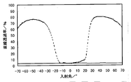
- FIG. 9 shows the incident angle dependence of the scattering characteristics of the light control plate 50 shown in FIG. 6 measured using the method shown in FIG.
- the vertical axis indicates the linear transmittance (an amount of parallel light emitted in the same direction as the incident direction when a predetermined amount of parallel light is incident), which is an index indicating the degree of scattering, and the horizontal axis indicates the incident angle.
- the solid line and the broken line in FIG. 9 respectively show the case where the light control plate 50 is rotated around the AA axis (through the plate structure) and the BB axis (parallel to the plate structure) in FIG. Show. As shown in FIG. 9, it can be seen that the characteristics of the light control plate 50 change by changing the axis.
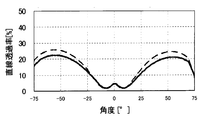
- FIG. 10 shows the incident angle dependence of the scattering characteristics of the anisotropic diffusion medium 1 shown in FIG. 7 measured using the method shown in FIG. As shown in FIG. 10, it can be seen that the characteristics of the anisotropic diffusion medium 1 do not change much even if the axis is changed.
- an object of the present invention is to provide a display device that can improve the problem of color change while having sufficient luminance even at a large viewing angle.
- anisotropic optical film including both the light control plate and the anisotropic diffusion medium
- anisotropic optical film including both the light control plate and the anisotropic diffusion medium
- the present invention has solved the above problems by the following technical configuration.
- a display device comprising a display device having a color change according to a viewing angle and an anisotropic optical film whose diffusivity changes depending on the incident angle of light, the anisotropic optical film having at least one scattering
- An angle formed between the scattering central axis and a direction in which the color change of the display device is minimized is in a range of 20 ° to 65 ° or ⁇ 20 ° to ⁇ 65 °.
- Display device (2)
- An angle formed by one of the scattering central axes and a direction in which the color change of the display device is minimized is in a range of 20 ° to 65 °, and the other of the scattering central axes is A display device, characterized in that the angle formed by the direction in which the color change of the display device is minimized is in the range of ⁇ 20 ° to ⁇ 65 °.
- the angle formed by the scattering central axis and the normal direction of the observation surface of the display device is in the range of ⁇ 60 ° to 60 °, as described in (1) or (2) above Display device.
- the display device is any one of a liquid crystal display device, a plasma display panel, and an organic EL device.
- the liquid crystal display device includes a liquid crystal cell in which liquid crystal is sandwiched between a pair of substrates, and a polarizing element.
- the present invention it is possible to provide a display device capable of improving the problem of color change while having sufficient luminance even at a large viewing angle.
- the “low refractive index region” and the “high refractive index region” are regions formed by a difference in local refractive index of the material constituting the anisotropic optical film and have a lower refractive index than the other. It is a relative one indicating whether it is expensive. These regions are formed when the material forming the anisotropic optical film is cured.
- “Diffusion center axis” means a direction in which the scattering characteristic coincides with the incident angle of light having a substantially target property with the incident angle as a boundary when the incident angle is changed. The reason for having “substantially target” is because it does not strictly have the target of optical characteristics.
- the diffusion center axis can be found by observing the inclination of the film cross section with an optical microscope or by observing the projection shape of light through the anisotropic optical film while changing the incident angle.
- the linear transmittance relates to the linear transmittance of light incident on the optical film, and is the ratio between the amount of transmitted light in the linear direction and the amount of incident light when incident from a certain incident angle. Is done.
- Linear transmittance (%) (Linear transmitted light amount / incident light amount) ⁇ 100
- Short wavelength and “long wavelength” are used in relative meanings, and do not mean a specific wavelength range.
- FIG. 1 is a diagram showing that the emitted light A from the light source 10 is reflected on the surface of the medium 20 and the reflected lights B, C, and D are obtained.
- the outgoing light A has a plurality of wavelengths in the visible light region.
- the scattering and reflection of light varies depending on the wavelength of light, and the light has a property of being easily diffused as the wavelength is shorter and difficult to diffuse as the wavelength is longer.
- the reflected light B is light in which the respective wavelengths are balanced
- the reflected light C is more unbalanced than the reflected light B (there is much short wavelength light and less long wavelength light).
- the light balance of the reflected light D is less than that of the reflected light C (a lot of short wavelength light and a little long wavelength light).
- color change the problem of color change accompanying the viewing angle
- the viewing angle of the reflected light B is the smallest and the viewing angle of the reflected light D is the largest.
- the phenomenon is not limited to the reflected light, and the same phenomenon can be seen in the diffused light (scattered light). Accordingly, not only the reflective display device but also the transmissive display device and the semi-transmissive / semi-reflective display device have a problem that the balance of light is similarly lost.
- the order of the light balance being easily lost is a reflective display device, a transflective display device, and a transmissive display device.
- the reflected light B will pass the anisotropic optical film 30, and the transmitted light B1 with little diffused light will be obtained. Although not shown in the figure, the reflected light B can be obtained as a diffused light together with the transmitted light B1.
- the reflected light C passes through the anisotropic optical film 30, it becomes diffused light C1 to C5.
- the diffused lights C1 and C5 have a substantially equal balance, and the diffused lights C2 and C4 have a substantially equal balance.
- the diffused light C3 has a short wavelength and a long wavelength.
- the diffused lights C2 and C4 have a shorter wavelength and a shorter wavelength than the diffused light C3.
- the diffused lights C1 and C5 have more short wavelength light and less long wavelength light than the diffused lights C2 and C4. Therefore, the reflected light B and the reflected light C have different characteristics of light passing through the anisotropic optical film 30. This is because the inclination of the structure (columnar structure, plate structure, or both) in the anisotropic optical film 30 contributes to the light diffusibility. Further, since the reflected light D exceeds a predetermined emission angle, it is totally reflected on the surface of the anisotropic optical film to become reflected light D1.
- the present invention makes it possible to supply light to a viewing angle region where a lack of luminance or a color change is likely to occur by selectively diffusing light incident on the anisotropic optical film 30 from a predetermined incident angle, An overall optimization of the light balance can be achieved.
- the inclination angle ⁇ of the inclination R of the structure (columnar structure, plate structure, or both) in the anisotropic optical film 30 is A range of 0 ° to 60 ° or a range of 0 ° to ⁇ 60 ° is preferable, and a range of 20 ° to 50 ° or a range of ⁇ 20 ° to ⁇ 50 ° is more preferable. If the inclination angle ⁇ is too small or too large, it is difficult to obtain the effect of improving the color change.
- the present invention uses a display device having a color change with the viewing angle.
- the display device is not particularly limited as long as it is a device for performing display, and examples thereof include a liquid crystal display device, a plasma display panel, and an organic EL device.
- the liquid crystal display device includes a liquid crystal cell sandwiched between a pair of substrates and a polarizing element.
- the form of the liquid crystal cell is not particularly limited, and examples thereof include a form having a liquid crystal sandwiched between a thin film transistor array substrate and a color filter substrate.
- the form of the polarizing plate is not particularly limited, but the form including the polarizing element and the support film in this order from the liquid crystal cell side, the form including the support film and the polarizing element in the order from the liquid crystal cell side, the first order from the liquid crystal cell side.
- the form containing 1 support film, a polarizing element, and a 2nd support film in order is mentioned.
- As said support film the thing similar to the transparent base
- the said polarizing plate is normally arrange
- the polarizing plate preferably further includes a retardation film. Thereby, the viewing angle dependency such as chromaticity of the liquid crystal display device can be further improved.
- the color change with the viewing angle is one of display performances of the display device. Specifically, the luminance (L *) and the number of colors in the direction in which the color change of the display device is minimum and the direction different from the direction by 60 degrees or ⁇ 60 degrees (whichever is sufficient) can be measured. (A *, b *) can be measured and calculated by ⁇ E * ab (color difference). Specifically, it can be obtained by the following equation. In the following equations, ⁇ L *, ⁇ a *, and ⁇ b * are calculated with the direction in which the color change of the display device is minimized as zero degrees.
- ⁇ E * ab [( ⁇ L *) 2 + ( ⁇ a *) 2 + ( ⁇ b *) 2 ] 1/2
- ⁇ L * L * (60 °) -L * (0 °)
- ⁇ a * a * (60 °) ⁇ a * (0 °)
- ⁇ b * b * (60 °) ⁇ b * (0 °)
- the lower limit value is preferable from the viewpoint of color change. However, if the lower limit value is too low, the haze increases and the image tends to be blurred and displayed, or the luminance in the front direction tends to decrease. It is preferable that it is, and it is more preferable that it is 20 or more.
- L * (0 °) in the normal direction is preferably as high as possible.
- the value of L * (0 °) varies greatly depending on the type of display device.
- the difference obtained by subtracting L * (0 °) in the normal direction from L * ( ⁇ 60 °) is preferably as low as possible. As the value of ⁇ L * is lowered, the difference between the luminance in the normal direction and the luminance in the 60 ° or ⁇ 60 ° direction is reduced, so that an image with less discomfort can be obtained even if the viewing angle changes.
- the difference obtained by subtracting L * (0 °) in the normal direction from L * (60 °) varies depending on the type of display device.
- the color change according to the viewing angle is observed when viewed from the front direction (the normal direction of the display surface of the display device, the viewing angle is 0 °) and when observed from the oblique direction (the viewing angle is greater than 0 °). , Meaning the hue is different. In general, the hue of the display device is larger in the direction closer to the front direction, but the opposite may be possible.
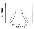
- FIG. 3 is an example showing that the luminance of the display device varies depending on the viewing angle.
- the luminance of the display device is a set having various wavelengths depending on the light source. However, if this is divided into a short wavelength and a long wavelength for convenience, the short wavelength is easy to diffuse and the long wavelength is difficult to diffuse. The shorter the wavelength, the more the longer the wavelength. In FIG. 3, short wavelengths and long wavelengths are not distinguished from each other and are described as a set of these.
- FIG. 3 shows a normal distribution centered on 0 °.
- the solid line in FIG. 3 is that of the prior art, and the luminance decreases at large viewing angles ( ⁇ 60 ° and 60 °).
- the dotted line in FIG. 3 shows the display device of the present invention.
- the present invention can provide a display device having sufficient luminance even at a large viewing angle by distributing a part of the luminance in the front direction (0 °) to a larger viewing angle.
- the present invention can also reduce the color change accompanying the viewing angle.
- the display apparatus which shows normal distribution centering on 0 degree is illustrated in FIG. 3, it is not restricted to this.
- the present invention can be applied to a display device that shows a normal distribution centered on 30 ° and a display device that shows a substantially target property centered on ⁇ 30 °.
- FIG. 4 shows a display device 100 having a display device 100 having a color change according to a viewing angle and an anisotropic optical film 30 whose diffusivity changes depending on the incident angle of light.
- the anisotropic optical film 30 is preferably provided on the observation surface side of the display device 100.
- the anisotropic optical film 30 has one scattering center axis.
- the direction in which the color change of the display device 100 is minimized can be arbitrarily determined in a range larger than ⁇ 90 ° and smaller than + 90 °, but is ⁇ 30 ° or more and + 30 ° or less. It is preferably -15 ° or more and + 15 ° or less.
- the angle formed by the scattering center axis of the anisotropic optical film 30 and the direction in which the color change of the display device 100 is minimized needs to be in the range of 20 ° to 65 ° or ⁇ 20 ° to ⁇ 65 °. is there. It is preferably in the range of 30 ° to 55 ° or ⁇ 30 ° to ⁇ 55 °. By setting this range, it is possible to distribute light in a direction in which the color change of the display device 100 is minimized to a larger viewing angle. As a result, it is possible to provide a display device having sufficient luminance even at a large viewing angle, and to reduce the color change associated with the viewing angle.
- the anisotropic optical film 30 There may be only one scattering center axis in the anisotropic optical film 30, and it may have two or more. It is also possible to laminate anisotropic optical films having different scattering center axes. When two anisotropic optical films having two or more scattering center axes or different scattering center axes are laminated in one anisotropic optical film, one of the scattering center axes is the display device.
- the angle formed between the direction in which the color change of the display device is minimum and the angle formed by the other of the scattering center axes is in the range of 20 ° to 65 °, and the direction in which the color change of the display device is minimized is ⁇ It is preferably in the range of 20 ° to -65 °.
- an angle formed by one of the scattering central axes and a direction in which the color change of the display device is minimized is in a range of 30 ° to 55 °, and the other of the scattering central axes is It is preferable that the angle between the direction in which the color change is minimal and the angle formed is in the range of ⁇ 30 ° to ⁇ 55 °. By setting it in this range, it is possible to obtain optical characteristics having substantially objectivity.
- the anisotropic optical film includes both those having a plate-like structure and those having a columnar structure therein. It is also possible to include these structures simultaneously. Comparing the improvement effect of the obtained color change between the one having a plate-like structure and the one having a columnar structure, the improvement effect of the color change is further improved by having the plate-like structure inside the anisotropic optical film. However, the improvement in the color change may change abruptly as the viewing angle changes, which may cause an unnatural impression to the viewer. On the other hand, although the anisotropic optical film has a columnar structure, the effect of improving the color change is slightly inferior, but the effect of improving the color change accompanying the change of the viewing angle changes gradually, which is unnatural to the observer. It is rare to have a strong impression. Further, when both the plate-like structure and the columnar structure are included in the anisotropic optical film, each has an intermediate property. The internal structure of the anisotropic optical film is preferably adjusted as appropriate according to the purpose of use.
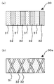
- FIG. 5 is a schematic view of the anisotropic optical film 30 of the present invention.
- region 32 are included alternately.
- adjacent high refractive index regions 32 may be crossed. When the adjacent high refractive index regions 32 are crossed, they may be crossed at all sites of the anisotropic optical film 30a or may be crossed partially. By crossing, the color change at the viewing angles in the two opposite directions can be improved. Further, in FIG. 5B, the case where the low refractive index region intersects instead of the high refractive index region may be different from the case where the inclination is changed.
- the refractive index difference (absolute value) between the low refractive index region and the high refractive index region is preferably 0.02 or more. More preferably, it is 0.03 or more, More preferably, it is 0.04 or more. The greater the refractive index difference, the greater the degree of anisotropy.
- the interface between the low refractive index region 31 and the high refractive index region 32 is drawn as a straight line, but the interface may be substantially linear or curved. Even if it is substantially linear or curved, the incident angle dependency as shown in FIG. 9 or 10 is exhibited.
- the interface between the low refractive index region 31 and the high refractive index region 32 is shown, but this interface may not exist substantially.
- the refractive index gradually increases or decreases, it is difficult to measure the refractive index.
- the local refractive index of the anisotropic optical film is measured a plurality of times, the lowest refractive index portion and the lowest refractive index portion are measured.
- the difference in refractive index from the portion having a high refractive index is 0.02 or more. More preferably, it is 0.03 or more, More preferably, it is 0.04 or more. The greater the refractive index difference, the greater the degree of anisotropy.
- the anisotropic optical film of the present invention can be produced by irradiating a specific photocurable compound with ultraviolet (UV) light under special conditions.
- UV ultraviolet
- the material for forming the anisotropic optical film of the present invention is composed of at least a monomer, oligomer, prepolymer, polymer or macromonomer of a photocurable compound and a photoinitiator. Alternatively, it is a material that is polymerized and solidified by irradiation with visible light. In addition to the photocurable compound, it is preferable to use a resin having a different curing method or the photocurable compound. Examples of resins with different curing methods include thermoplastic resins and thermosetting resins.
- a combination of a photocurable compound and a thermoplastic resin, a combination of a photocurable compound and a thermosetting resin, or a combination of a photocurable compound, a thermoplastic resin, and a thermosetting resin can be appropriately employed.
- a difference in refractive index occurs due to the difference in density. This is because a portion having a high UV irradiation intensity has a fast curing speed, and thus the cured material moves around the cured region, and as a result, a region having a higher refractive index and a region having a lower refractive index are formed.
- the photocurable compound is a monomer, oligomer, prepolymer or macromonomer having a radical polymerizable or cationic polymerizable functional group.
- the radical polymerizable functional group include an acryloyl group, a methacryloyl group, and an allyl group.
- the cationic polymerizable functional group include an epoxy group and an oxetane group. There are no particular restrictions on the type and number of these functional groups, but it is preferable to have a polyfunctional acryloyl group or methacryloyl group because the higher the functional groups, the higher the crosslink density and the greater the difference in refractive index. .
- the radically polymerizable compound mainly contains one or more unsaturated double bonds in the molecule, and specifically includes methyl acrylate, epoxy acrylate, urethane acrylate, polyester acrylate, polyether acrylate, polybutadiene acrylate, and the like.
- a compound having at least one epoxy group, vinyl ether group or oxetane group in the molecule can be used.
- the compounds having an epoxy group include 2-ethylhexyl diglycol glycidyl ether, glycidyl ether of biphenyl, bisphenol A, hydrogenated bisphenol A, bisphenol F, bisphenol AD, bisphenol S, tetramethylbisphenol A, tetramethylbisphenol F, tetrachloro Diglycidyl ethers of bisphenols such as bisphenol A and tetrabromobisphenol A, polyglycidyl ethers of novolac resins such as phenol novolak, cresol novolak, brominated phenol novolak, orthocresol novolak, ethylene glycol, polyethylene glycol, polypropylene glycol, Butanediol, 1,6-hexanediol, neopentyl glycol, trimethyl
- Examples of the compound having a vinyl ether group include diethylene glycol divinyl ether, triethylene glycol divinyl ether, butanediol divinyl ether, hexanediol divinyl ether, cyclohexanedimethanol divinyl ether, hydroxybutyl vinyl ether, ethyl vinyl ether, dodecyl vinyl ether, and trimethylolpropane trivinyl ether. , Propenyl ether propylene carbonate and the like, but are not limited thereto. Vinyl ether compounds are generally cationically polymerizable, but radical polymerization is also possible by combining with acrylates.
- the above cationic polymerizable compounds may be used alone or in combination.
- the photopolymerizable compound is not limited to the above.
- fluorine atoms (F) may be introduced into the photopolymerizable compound in order to reduce the refractive index, and in order to increase the refractive index, Sulfur atoms (S), bromine atoms (Br), and various metal atoms may be introduced.
- thermoplastic resin examples include polyester, polyether, polyurethane, polyamide, polyepoxide, polystyrene, polycarbonate, polyacetal, polyvinyl alcohol, polyvinyl acetate, polyvinyl butyral, an acrylic resin, and a copolymer or a modified product thereof.
- a thermoplastic resin it is dissolved using a solvent in which the thermoplastic resin dissolves, and after application and drying, the photocurable compound is cured with ultraviolet rays to form an anisotropic optical film.
- the solvent may be any solvent as long as it can dissolve the thermoplastic resin.
- alcohol such as ethanol, isopropanol or butanol
- ketone such as acetone
- ester such as ethyl acetate
- ether such as tetrahydrofuran, hexane, benzene
- Aliphatic aromatic and halogenated hydrocarbons such as toluene and chloroform.
- thermosetting resin examples include epoxy resins, phenol resins, melamine resins, urea resins, unsaturated polyesters, copolymers thereof, and modified products.
- the anisotropic optical film is formed by curing the thermosetting resin by appropriately heating after curing the photocurable compound with ultraviolet rays.
- Photoinitiators that can polymerize radically polymerizable compounds include benzophenone, benzyl, Michler's ketone, 2-chlorothioxanthone, 2,4-diethylthioxanthone, benzoin ethyl ether, benzoin isopropyl ether, benzoin isobutyl ether, 2,2- Diethoxyacetophenone, benzyldimethyl ketal, 2,2-dimethoxy-1,2-diphenylethane-1-one, 2-hydroxy-2-methyl-1-phenylpropan-1-one, 1-hydroxycyclohexyl phenyl ketone, 2 -Methyl-1- [4- (methylthio) phenyl] -2-morpholinopropanone-1, 1- [4- (2-hydroxyethoxy) -phenyl] -2-hydroxy-2-methyl-1-propane-1 -On, bis (cyclo Ntadienyl) -bis
- the photoinitiator of a cationic polymerizable compound is a compound that generates an acid by light irradiation and can polymerize the above-mentioned cationic polymerizable compound with the generated acid.
- an onium salt or a metallocene complex is used.
- the onium salt a diazonium salt, a sulfonium salt, an iodonium salt, a phosphonium salt, a selenium salt, or the like is used, and these counter ions include anions such as BF 4 ⁇ , PF 6 ⁇ , AsF 6 ⁇ , SbF 6 ⁇ and the like. Used.
- Specific examples include 4-chlorobenzenediazonium hexafluorophosphate, triphenylsulfonium hexafluoroantimonate, triphenylsulfonium hexafluorophosphate, (4-phenylthiophenyl) diphenylsulfonium hexafluoroantimonate, (4-phenylthiophenyl) diphenyl.
- a functional additive In order to impart an effect of improving color change to the anisotropic optical film, it is preferable to contain a functional additive.
- the functional additive include (a) a condensed silane compound, (b) ultrafine particles with a modified surface, and (c) a softening agent.
- (A) Condensed silane compound The silane is one having 1, 2, 3 or 4, preferably 2 or 3, hydrolyzable groups, and a mixture thereof.
- hydrolyzable groups are hydrogen or halogens such as F, Cl, Br or I, alkoxy, preferably C1-6 alkoxy such as methoxy, ethoxy, n-propoxy, i-propoxy and butoxy; aryloxy, preferably For example C6-10 aryloxy such as phenoxy; acyloxy such as acetoxy or propionyloxy; alkylcarbonyl, preferably C2-7 alkylcarbonyl such as acetyl; amino, preferably 1 to 12 in alkyl group, especially 1 Monoalkylamino or dialkylamino having ⁇ 6 carbon atoms.
- silanes are, for example, methacryloxypropyltrimethoxysilane, acryloxypropyltrimethoxysilane, dimethyldimethoxysilane, dimethyldiethoxysilane, 3-glycidyloxy-propyltrimethoxysilane, glycidyloxy-propyltriethoxysilane, vinyltriethoxy Silane and methyltriethoxysilane.
- the partial condensation of the silane can be carried out, for example, with a hydrolyzing agent such as water, aqueous HCl, aqueous HNO 3 or aqueous ammonia, using a short equivalent, for example 0.3 to 0.9 times the stoichiometric amount. it can.
- Silane may be fully condensed.
- the amount of hydrolyzing agent is preferably assigned in this case so as to obtain an inorganic condensation ratio of 33 to 100%.
- the average inorganic condensation rate of 33% means that, for example, approximately one of the three hydrolyzable residues of silane is condensed to form —Si—O—Si— crosslinks.
- the condensation with a hydrolyzing agent is preferably carried out at a temperature between 5 and 40 ° C.
- the condensation of silane may be performed by a method of polymerizing by UV irradiation.
- the organic conversion rate of silane is preferably 0 to 95%, more preferably 5 to 60%.
- ultrafine particles described later may be generated by hydrolysis and condensation of the precursor (preferably alkoxide).
- the blending amount of the condensed silane compound is preferably 0.00120% by mass with respect to the total solid content of the anisotropic optical film.
- Ultra fine particles whose surface is modified are preferably oxides, ZnO, CdO, SiO 2 , TiO 2 , ZrO 2 , CeO 2 , SnO 2 , Al 2 O 3 , In 2.
- the surface group can be an organic polymerizable and / or condensation polymerizable group that is sensitive to radicals, cations or anions, thermal or photochemical polymerization, or thermal or photochemical condensation polymerization.
- surface groups having (meth) acryl, allyl, vinyl or epoxy groups are preferred, with (meth) acryl and epoxy groups being particularly preferred.
- the main relevant condensation polymerizable groups are hydroxyl, carboxyl and amino groups which can be used between nanoscale particles and silanes to obtain ether, ester and amide linkages.
- a compound containing a polymerizable group for example, an unsaturated carboxylic acid, particularly methacrylic acid, acrylic acid, and acrylosilane and / or an unsaturated ⁇ -diketone is modified. Just do it.
- the organic group present on the surface of the ultrafine particles and containing a polymerizable and / or condensation polymerizable group preferably has a molecular weight of less than 300, in particular less than 200.
- the ultrafine particles preferably have a diameter (primary particle size) of 100 nm or less, particularly 50 nm or less. There is no particular restriction on the lower limit, but for practical reasons this lower limit is generally 0.5 nm, in particular 1 nm, often 4 nm.
- the surface of the ultrafine particles is first subjected to a compound containing a polymerizable group, such as an unsaturated carboxylic acid, particularly methacrylic acid, acrylic acid, and acrylosilane and / or an unsaturated ⁇ diketone. Can be modified by reacting with.
- a compound containing a polymerizable group such as an unsaturated carboxylic acid, particularly methacrylic acid, acrylic acid, and acrylosilane and / or an unsaturated ⁇ diketone.
- the blending amount of the ultrafine particles whose surface has been modified is preferably 0.01 to 20% by mass with respect to the total solid content of the anisotropic optical film.
- (C) Softeners As softeners, all compounds with elastic or softening properties are suitable in principle according to DIN 55945 (December 1988), but mainly those of the ester type. Plasticizers from the following groups are preferred: acyclic aliphatic dicarboxylic esters such as di-n-octyl adipate, bis- (2-ethylhexyl) adipate, esters of adipic acid such as diisodecyl adipate, sebacic acid Dibutyl, dioctyl sebacate and bis- (2-ethylhexyl) sebacate; esters of C6-C12 dicarboxylic acids with polyalkylene glycols, such as triethylene glycol bis- (n-heptanoate), triethylene glycol bis- (2-ethyl) Hexanoate), triethylene glycol bis- (isonanoate); esters of C6-C12 dicarboxylic acids and polyalkylene glycol
- the blending amount of the softening agent is preferably 0.1 to 20% by mass with respect to the total solid content of the anisotropic optical film.
- the photoinitiator is 0.01 to 10 parts by weight, preferably 0.1 to 7 parts by weight, more preferably about 0.1 to 5 parts by weight with respect to 100 parts by weight of the photocurable compound. Blended. This is because if less than 0.01 parts by mass, the photocurability decreases, and if more than 10 parts by mass is blended, only the surface is cured and the internal curability is reduced. This is because the reduction and the inhibition of formation of the plate-like structure are caused.
- photoinitiators are usually used by dissolving the powder directly in the mixture of the above composition, but if the solubility is poor, the photoinitiator is dissolved in a very small amount of solvent in advance at a high concentration. Can also be used.
- a solvent is more preferably photopolymerizable, and specific examples thereof include propylene carbonate and ⁇ -butyrolactone. It is also possible to add various known dyes and sensitizers in order to improve the photopolymerizability.
- a thermosetting initiator capable of curing the photopolymerizable compound by heating can be used in combination with the photoinitiator.
- thermosetting initiator is preferably an organic peroxide in the form of diacyl peroxide, peroxydicarbonate, alkyl perester, dialkyl peroxide, perketal, ketone peroxide and alkyl hydroperoxide.
- examples of such thermosetting initiators are dibenzoyl peroxide, t-butyl perbenzoate and azobisisobutyronitrile.
- An example of a cationic thermal initiator is 1-methylimidazole.
- the thermosetting initiator may be contained in an amount of about 0.01 to 20 parts by mass with respect to 100 parts by mass of the thermosetting resin.
- the photocurable compound can be cured to form an anisotropic optical film.
- a plurality of materials constituting the anisotropic optical film can be mixed.
- known additives such as a plasticizer, an antioxidant, a light stabilizer, a surfactant, and a leveling agent can be added to the composition as necessary.
- plasticizers, surfactants, leveling agents, plasticizers, etc. are effective for improving film-forming properties, and include plasticizers such as phthalic polyester and adipic acid polyester, and silicone and acrylic leveling agents.
- the addition amount is preferably 0.5 to 10% by weight in the total composition.
- the ratio of the photocurable compound having a silicone skeleton to the compound having no silicone skeleton is preferably in the range of 15:85 to 85:15 by mass ratio. More preferably, it is in the range of 30:70 to 70:30. By setting it in this range, the phase separation between the low refractive index region and the high refractive index region can easily proceed. If the ratio of the photocurable compound having a silicone skeleton is less than the lower limit value or exceeds the upper limit value, the phase separation is difficult to proceed, and the problem of insufficient anisotropy is difficult to solve.
- the content is preferably 10 to 60% by mass based on the total photocurable resin composition. If the addition amount is less than the lower limit, the effect of disturbing the molecular orientation is lost and the effect of lowering the phase difference cannot be expected. If the addition amount is too large, the orientation is too disturbed and the original optical anisotropy is impaired. A more preferable blending amount is 15 to 45% by mass, and a sufficient decrease in retardation can be exhibited.
- the anisotropic optical film of the present invention can realize both anisotropy and a low retardation that could not be achieved conventionally by appropriately selecting the compound and the blending amount thereof, and the retardation is an optical film. It can be made sufficiently low 25 nm or less. Furthermore, it is possible to make the thickness 10 nm or less, and the retardation can be equivalent to that of a TAC film, COP film or polycarbonate (PC) sheet conventionally used as a low retardation film. It is also possible to do. That is, the anisotropic optical film of the present invention can be used as a protective film for a polarizing plate.
- the anisotropic optical film obtained by the present invention since the anisotropic optical film obtained by the present invention has a low phase difference, it hardly causes light leakage even when it exists between the crossed Nicols of the polarizing plate, and between the parallel Nicols of the polarizing plate. Even when it is present, optical loss is less likely to occur, and when used for a display or the like, a decrease in luminance is suppressed, contributing to an improvement in contrast.
- the manufacturing method (process) of the anisotropic optical film of this invention is demonstrated.
- the above-mentioned anisotropic optical film forming material photocurable resin composition
- a suitable substrate such as a transparent polyethylene terephthalate (PET) film
- PET transparent polyethylene terephthalate
- the solvent is evaporated by drying as necessary, and the dry film thickness is 10 to 500 ⁇ m, more preferably 20 to 200 ⁇ m, and still more preferably 30 to 100 ⁇ m.
- the dry film thickness is less than 10 ⁇ m, the light diffusibility obtained through the UV irradiation process described later is poor, which is not preferable.
- the dry film thickness exceeds 500 ⁇ m, the overall diffusibility is too strong, and it becomes difficult to obtain the characteristic anisotropy of the present invention, and it is not preferable because of cost increase and incompatibility with thinning applications.
- a release film or a mask described later can be laminated on the coating film to produce a photosensitive laminate.
- Method of providing a photocurable resin composition in a sheet form on a substrate a normal coating method or printing method is applied. Specifically, air doctor coating, bar coating, blade coating, knife coating, reverse coating, transfer roll coating, gravure roll coating, kiss coating, cast coating, spray coating, slot orifice coating, calendar coating, dam coating, dip coating Coating such as die coating, intaglio printing such as gravure printing, printing such as stencil printing such as screen printing, and the like can be used.
- the photocurable resin composition has a low viscosity, a weir with a certain height can be provided around the substrate, and the photocurable resin composition can be cast in the area surrounded by the weir.
- a short arc ultraviolet ray generating light source As a light source for irradiating the coating film with light, a short arc ultraviolet ray generating light source is usually used. Specifically, a high pressure mercury lamp, a low pressure mercury lamp, a metahalide lamp, a xenon lamp, or the like can be used.
- the light beam applied to the photocurable resin composition containing the photocurable compound needs to include a wavelength capable of curing the photocurable compound. Usually, light having a wavelength centered at 365 nm of a mercury lamp is emitted. Used.
- the shape of the light source is preferably linear or dot-like, and a light source that looks substantially linear when viewed from the irradiated position may be used.
- a linear light source When forming a plate-like structure in the anisotropic optical film, it is preferable to use a linear light source, and when forming a columnar structure, a point light source is preferably used.
- a linear light source and a point light source may be used.
- a method for obtaining a linear light beam a known method using various light sources and lenses can be used.
- a simple method an example is shown in which a diffused light source is converted into a parallel light beam using a Fresnel lens or the like, and the parallel light beam is further converted into a linear light beam diffused in only one direction via a lenticular lens. This is not the case.
- a reflecting mirror is arranged behind the light source so that the light is emitted as a point light source in a predetermined direction, and the light is further emitted into the Fresnel.
- the lens can make parallel light.
- a Fresnel lens is a lens in which a normal lens is divided into concentric regions to reduce the thickness, and has a saw-like cross section. When the light beam emitted from the point light source passes through the Fresnel lens, the directions of the light beams having different directions are unified in one direction to become parallel light beams.
- a Fresnel lens is not necessarily required, and various methods including a laser can be used. .
- a part of the parallel light beam is converted into a linear light beam by causing the parallel light beam described above to be incident on the flat surface of the lenticular lens and to be emitted from the uneven surface of the lenticular lens. That is, a parallel light beam and a linear light beam can be obtained through the lenticular lens.
- the above-described UV irradiation method using a lenticular lens is one method for producing the anisotropic optical film of the present invention, and the present invention is not limited thereto.
- a fine structure having a high and low refractive index according to the present invention is formed by the step of irradiating the photocurable composition layer with light having a planar fan-shaped spread.
- the light to irradiate has a wavelength which can harden the said photocurable composition.
- the illuminance of the UV light applied to the coating film is preferably in the range of 0.01 to 100 mW / cm 2 , more preferably 0.1 to The range is 20 mW / cm 2 . If the illuminance is 0.01 mW / cm 2 or less, it takes a long time to cure, resulting in poor production efficiency. If the illuminance is 100 mW / cm 2 or more, the photo-curing compound is cured too quickly to form a structure, This is because the desired anisotropic diffusion characteristic cannot be expressed.
- the UV irradiation time is not particularly limited, but is 10 to 180 seconds, more preferably 30 to 120 seconds. Then, the anisotropic optical film of this invention can be obtained by peeling a release film.
- the anisotropic optical film of the present invention is obtained by forming a specific internal structure in a photocurable composition by irradiating with low-intensity UV light for a relatively long time as described above. For this reason, unreacted monomer components remain by such UV irradiation alone, and stickiness may occur, which may cause problems in handling properties and durability.
- the residual monomer can be polymerized by additional irradiation with UV light having a high illuminance of 1000 mW / cm 2 or more.
- the UV irradiation at this time is preferably performed from the opposite side (base material side) of the direction in which the UV irradiation was performed first.
- Display device As a display device comprising the display device constituting the present invention and an anisotropic optical film, a liquid crystal display device (LCD), a plasma display panel (PDP), an electroluminescence display (ELD), and a cathode ray tube display device (CRT) It can be applied to display devices such as surface electric field display (SED) and electronic paper.
- the anisotropic optical film of the present invention can be preferably used for a transmissive, reflective, or transflective liquid crystal display device, top emission type, or bottom emission type organic EL. This is because these display devices tend to cause a color shift problem. In a liquid crystal display device, light is twisted by a liquid crystal and a color shift occurs.
- the bottom emission type is particularly likely to cause a color shift problem. This is because reflected light is used.
- the anisotropic optical film of the present invention has few problems of adhesive strength, and can be used by being bonded to a desired place via an adhesive layer or an adhesive layer.
- An anisotropic optical film constituting the present invention and an anisotropic optical film of a comparative example were produced according to the following method.
- Example 1 A partition wall having a height of 0.2 mm was formed with a curable resin on the entire periphery of the edge of a PET film (trade name: A4300, manufactured by Toyobo Co., Ltd.) having a thickness of 100 ⁇ m and a size of 76 ⁇ 26 mm. This was filled with the following photocurable resin composition and covered with another PET film.
- a PET film trade name: A4300, manufactured by Toyobo Co., Ltd.
- Ultraviolet rays converted into linear rays through a lenticular lens are irradiated for 1 minute at an irradiation intensity of 10 mW / cm 2 so as to be at an angle of 60 ° from the normal direction of the liquid film, and FIG.
- the anisotropic optical film of Example 1 having a large number of linear minute regions as shown in FIG. From there, the PET film was peeled off to obtain the anisotropic optical film of the present invention.
- Example 2 An anisotropic optical film of the present invention was obtained in the same manner as in Example 1 except that the ultraviolet ray was changed to an angle of 45 ° from the normal direction of the liquid film.
- Example 3 The anisotropic optical film of the present invention was prepared in the same manner as in Example 1 except that the thickness of the liquid film was 0.05 mm and the ultraviolet ray was changed to an angle of 45 ° from the normal direction of the liquid film. Obtained.
- Comparative Example 1 A commercially available fine particle dispersion type isotropic diffusive film was prepared without producing an anisotropic optical film constituting the present invention.
- the total film thickness of the prepared isotropic diffusion film was 120 ⁇ m, HAZE was 80%, and total light transmittance was 85%.
- the weight average molecular weight (Mw) of the silicone, urethane, and acrylate used in Examples 1 to 3 and Comparative Examples 1 and 2 was measured as a polystyrene-converted molecular weight using the GPC method under the following conditions.
- Degasser DG-980-51 (manufactured by JASCO Corporation) Pump: PU-980-51 (manufactured by JASCO Corporation) Autosampler: AS-950 (manufactured by JASCO Corporation) Thermostatic chamber: C-965 (manufactured by JASCO Corporation) Column: Shodex KF-806L x 2 (made by Showa Denko KK) Detector: RI (SHIMAMURA YDR-880) Temperature: 40 ° C Eluent: THF Injection volume: 150 ⁇ l Flow rate: 1.0ml / min Sample concentration: 0.2%
- the anisotropic optical films of Examples and Comparative Examples were evaluated using a variable angle photometer goniophotometer (manufactured by Genesia Co., Ltd.) that can arbitrarily change the light projecting angle of the light source and the light receiving angle of the light receiver.
- the light receiving part was fixed at a position where the light traveling straight from the light source was received, and the anisotropic optical films obtained in Examples and Comparative Examples were set in the sample holder therebetween. As shown in FIG. 8, the sample was rotated as the rotation axis (L), and the linear transmitted light amount corresponding to each incident angle was measured.
- the rotation axis (L) is the same axis as the BB axis in the sample structure shown in FIG.
- the linear transmitted light amount was measured by measuring the wavelength in the visible light region using a visibility filter.
Landscapes
- Physics & Mathematics (AREA)
- General Physics & Mathematics (AREA)
- Optics & Photonics (AREA)
- Nonlinear Science (AREA)
- Chemical & Material Sciences (AREA)
- Mathematical Physics (AREA)
- Crystallography & Structural Chemistry (AREA)
- Dispersion Chemistry (AREA)
- Optical Elements Other Than Lenses (AREA)
- Liquid Crystal (AREA)
- Devices For Indicating Variable Information By Combining Individual Elements (AREA)
- Polarising Elements (AREA)
Priority Applications (3)
| Application Number | Priority Date | Filing Date | Title |
|---|---|---|---|
| CN201380063790.1A CN104854643B (zh) | 2012-12-07 | 2013-12-06 | 显示装置 |
| US14/650,481 US9581738B2 (en) | 2012-12-07 | 2013-12-06 | Display apparatus |
| KR1020157017778A KR102047741B1 (ko) | 2012-12-07 | 2013-12-06 | 표시장치 |
Applications Claiming Priority (2)
| Application Number | Priority Date | Filing Date | Title |
|---|---|---|---|
| JP2012268784A JP5695633B2 (ja) | 2012-12-07 | 2012-12-07 | 表示装置 |
| JP2012-268784 | 2012-12-07 |
Publications (1)
| Publication Number | Publication Date |
|---|---|
| WO2014088086A1 true WO2014088086A1 (ja) | 2014-06-12 |
Family
ID=50883498
Family Applications (1)
| Application Number | Title | Priority Date | Filing Date |
|---|---|---|---|
| PCT/JP2013/082766 Ceased WO2014088086A1 (ja) | 2012-12-07 | 2013-12-06 | 表示装置 |
Country Status (5)
| Country | Link |
|---|---|
| US (1) | US9581738B2 (https=) |
| JP (1) | JP5695633B2 (https=) |
| KR (1) | KR102047741B1 (https=) |
| CN (1) | CN104854643B (https=) |
| WO (1) | WO2014088086A1 (https=) |
Cited By (1)
| Publication number | Priority date | Publication date | Assignee | Title |
|---|---|---|---|---|
| JP2017187770A (ja) * | 2016-03-31 | 2017-10-12 | 株式会社巴川製紙所 | 異方性光学フィルム及びその製造方法 |
Families Citing this family (12)
| Publication number | Priority date | Publication date | Assignee | Title |
|---|---|---|---|---|
| JP6981984B2 (ja) * | 2016-09-14 | 2021-12-17 | 株式会社巴川製紙所 | 反射型表示装置用光拡散フィルム積層体及びこれを用いた反射型表示装置 |
| JP6993976B2 (ja) * | 2016-09-14 | 2022-01-14 | 株式会社巴川製紙所 | 反射型表示装置用光拡散フィルム積層体及びこれを用いた反射型表示装置 |
| JP6955885B2 (ja) * | 2017-03-31 | 2021-10-27 | リンテック株式会社 | プロジェクションスクリーン |
| TWI759451B (zh) * | 2017-03-31 | 2022-04-01 | 日商巴川製紙所股份有限公司 | 使用各向異性光學膜之導光積層體及使用該導光積層體的面狀光源裝置 |
| JP6616921B1 (ja) * | 2018-05-14 | 2019-12-04 | 株式会社巴川製紙所 | ヘッドマウントディスプレイ |
| KR102649006B1 (ko) | 2018-07-06 | 2024-03-20 | 삼성전자주식회사 | 디스플레이 장치 |
| JP7475333B2 (ja) * | 2019-03-29 | 2024-04-26 | 株式会社巴川コーポレーション | 異方性光学フィルムを用いた反射型表示装置 |
| KR102867915B1 (ko) * | 2019-10-24 | 2025-10-01 | 엘지디스플레이 주식회사 | 시야각 조절 필름 및 이를 포함하는 표시 장치 |
| TWI877340B (zh) * | 2020-03-31 | 2025-03-21 | 日商巴川集團股份有限公司 | 異方性光擴散膜及顯示裝置 |
| KR102162846B1 (ko) * | 2020-08-20 | 2020-10-07 | 에스케이씨하이테크앤마케팅(주) | 광학 복합 시트 및 이를 포함하는 표시 장치 |
| JP2023148723A (ja) * | 2022-03-30 | 2023-10-13 | リンテック株式会社 | 視野角制御フィルム |
| DE102023114511A1 (de) * | 2023-06-02 | 2024-12-05 | Bayerische Motoren Werke Aktiengesellschaft | Anzeigevorrichtung für ein Kraftfahrzeug und zugehöriges Kraftfahrzeug |
Citations (5)
| Publication number | Priority date | Publication date | Assignee | Title |
|---|---|---|---|---|
| JP2004341309A (ja) * | 2003-05-16 | 2004-12-02 | Fuji Photo Film Co Ltd | 分光異方性光散乱フィルム、偏光板および液晶表示装置 |
| JP2007249182A (ja) * | 2006-02-17 | 2007-09-27 | Sharp Corp | 表示装置 |
| JP2012155068A (ja) * | 2011-01-25 | 2012-08-16 | Sony Mobile Display Corp | 表示パネル、表示装置および電子機器 |
| JP2012208408A (ja) * | 2011-03-30 | 2012-10-25 | Japan Display West Co Ltd | 表示装置および電子機器 |
| JP2012226158A (ja) * | 2011-04-20 | 2012-11-15 | Toyobo Co Ltd | 視野角向上フィルム、視野角向上フィルム積層体及び液晶表示装置 |
Family Cites Families (14)
| Publication number | Priority date | Publication date | Assignee | Title |
|---|---|---|---|---|
| DE3789858T2 (de) | 1986-12-18 | 1994-09-01 | Nippon Sheet Glass Co Ltd | Platten für Lichtkontrolle. |
| JP2547417B2 (ja) | 1987-08-07 | 1996-10-23 | 日本板硝子株式会社 | 光制御板の製造方法 |
| JP2004264345A (ja) | 2003-02-03 | 2004-09-24 | Nitto Denko Corp | 位相差フィルムおよびその製造方法 |
| US6995820B2 (en) * | 2003-05-16 | 2006-02-07 | Fuji Photo Film Co., Ltd. | Anisotropic spectral scattering films, polarizers and liquid crystal displays |
| JP2005265915A (ja) | 2004-03-16 | 2005-09-29 | Tomoegawa Paper Co Ltd | 異方性拡散媒体及びその製造方法 |
| US20070110957A1 (en) | 2004-03-16 | 2007-05-17 | Kensaku Higashi | Anisotropic diffusing medium and production method therefor |
| US20070011097A1 (en) | 2005-07-06 | 2007-01-11 | Andreas Eckleder | License server and user processor |
| JP2007079855A (ja) | 2005-09-13 | 2007-03-29 | I L C:Kk | 情報処理装置、プログラム提供装置、プログラム提供方法、および該方法をコンピュータに実行させるプログラム |
| CN100504544C (zh) * | 2006-02-17 | 2009-06-24 | 夏普株式会社 | 显示装置 |
| US7800719B2 (en) * | 2006-02-17 | 2010-09-21 | Sharp Kabushiki Kaisha | Display |
| JP5090861B2 (ja) * | 2007-11-07 | 2012-12-05 | 株式会社巴川製紙所 | 異方性拡散媒体 |
| JP5320250B2 (ja) | 2009-10-14 | 2013-10-23 | 株式会社日立製作所 | 透明構造体、光源モジュール並びにこれを用いた照明装置,液晶表示装置及び映像表示装置 |
| JP5738006B2 (ja) * | 2011-03-01 | 2015-06-17 | 株式会社巴川製紙所 | 光学フィルム |
| CN102778711B (zh) | 2011-05-13 | 2015-03-11 | 夏普株式会社 | 光扩散部件和显示装置 |
-
2012
- 2012-12-07 JP JP2012268784A patent/JP5695633B2/ja active Active
-
2013
- 2013-12-06 CN CN201380063790.1A patent/CN104854643B/zh active Active
- 2013-12-06 KR KR1020157017778A patent/KR102047741B1/ko active Active
- 2013-12-06 WO PCT/JP2013/082766 patent/WO2014088086A1/ja not_active Ceased
- 2013-12-06 US US14/650,481 patent/US9581738B2/en active Active
Patent Citations (5)
| Publication number | Priority date | Publication date | Assignee | Title |
|---|---|---|---|---|
| JP2004341309A (ja) * | 2003-05-16 | 2004-12-02 | Fuji Photo Film Co Ltd | 分光異方性光散乱フィルム、偏光板および液晶表示装置 |
| JP2007249182A (ja) * | 2006-02-17 | 2007-09-27 | Sharp Corp | 表示装置 |
| JP2012155068A (ja) * | 2011-01-25 | 2012-08-16 | Sony Mobile Display Corp | 表示パネル、表示装置および電子機器 |
| JP2012208408A (ja) * | 2011-03-30 | 2012-10-25 | Japan Display West Co Ltd | 表示装置および電子機器 |
| JP2012226158A (ja) * | 2011-04-20 | 2012-11-15 | Toyobo Co Ltd | 視野角向上フィルム、視野角向上フィルム積層体及び液晶表示装置 |
Cited By (1)
| Publication number | Priority date | Publication date | Assignee | Title |
|---|---|---|---|---|
| JP2017187770A (ja) * | 2016-03-31 | 2017-10-12 | 株式会社巴川製紙所 | 異方性光学フィルム及びその製造方法 |
Also Published As
| Publication number | Publication date |
|---|---|
| JP2014115421A (ja) | 2014-06-26 |
| US9581738B2 (en) | 2017-02-28 |
| KR102047741B1 (ko) | 2019-11-25 |
| US20150338698A1 (en) | 2015-11-26 |
| CN104854643B (zh) | 2018-11-27 |
| CN104854643A (zh) | 2015-08-19 |
| JP5695633B2 (ja) | 2015-04-08 |
| KR20150093751A (ko) | 2015-08-18 |
Similar Documents
| Publication | Publication Date | Title |
|---|---|---|
| JP5695633B2 (ja) | 表示装置 | |
| JP6483030B2 (ja) | 異方性光学フィルム | |
| TWI760456B (zh) | 防眩性薄膜及顯示裝置 | |
| TWI654087B (zh) | 各向異性光學膜 | |
| JP6616921B1 (ja) | ヘッドマウントディスプレイ | |
| JP6039911B2 (ja) | 偏光板用異方性光学フィルムおよびその製造方法 | |
| WO2007111026A1 (ja) | 光学フィルム | |
| JPWO2014084361A1 (ja) | 異方性光学フィルム | |
| JP6093113B2 (ja) | 異方性光学フィルム | |
| JP5977955B2 (ja) | 異方性光学フィルムおよびその製造方法 | |
| JP5947410B2 (ja) | 表示装置 | |
| JP6542007B2 (ja) | 異方性光学フィルム及びその製造方法 | |
| JP2015222441A (ja) | 異方性光学フィルム | |
| JP6581329B1 (ja) | ヘッドマウントディスプレイ | |
| CN112088578B (zh) | 头戴式显示器 | |
| JP2017187770A (ja) | 異方性光学フィルム及びその製造方法 | |
| TW202246860A (zh) | 各向異性光擴散膜及顯示裝置 | |
| WO2021200891A1 (ja) | 異方性光拡散フィルムおよび表示装置 |
Legal Events
| Date | Code | Title | Description |
|---|---|---|---|
| 121 | Ep: the epo has been informed by wipo that ep was designated in this application |
Ref document number: 13861156 Country of ref document: EP Kind code of ref document: A1 |
|
| NENP | Non-entry into the national phase |
Ref country code: DE |
|
| WWE | Wipo information: entry into national phase |
Ref document number: 14650481 Country of ref document: US |
|
| ENP | Entry into the national phase |
Ref document number: 20157017778 Country of ref document: KR Kind code of ref document: A |
|
| 122 | Ep: pct application non-entry in european phase |
Ref document number: 13861156 Country of ref document: EP Kind code of ref document: A1 |