WO2014087502A1 - 計測装置、プローブ部及び接続ケーブル - Google Patents
計測装置、プローブ部及び接続ケーブル Download PDFInfo
- Publication number
- WO2014087502A1 WO2014087502A1 PCT/JP2012/081519 JP2012081519W WO2014087502A1 WO 2014087502 A1 WO2014087502 A1 WO 2014087502A1 JP 2012081519 W JP2012081519 W JP 2012081519W WO 2014087502 A1 WO2014087502 A1 WO 2014087502A1
- Authority
- WO
- WIPO (PCT)
- Prior art keywords
- drive current
- main body
- light source
- reference voltage
- light
- Prior art date
Links
- 239000000523 sample Substances 0.000 title claims abstract description 139
- 238000005259 measurement Methods 0.000 title claims abstract description 50
- 230000003287 optical effect Effects 0.000 claims abstract description 21
- 230000003321 amplification Effects 0.000 claims description 19
- 238000003199 nucleic acid amplification method Methods 0.000 claims description 19
- 230000017531 blood circulation Effects 0.000 claims description 7
- 238000004364 calculation method Methods 0.000 claims description 6
- 238000001514 detection method Methods 0.000 claims description 3
- 230000001105 regulatory effect Effects 0.000 abstract 1
- 238000000034 method Methods 0.000 description 21
- 230000008569 process Effects 0.000 description 15
- 239000004065 semiconductor Substances 0.000 description 14
- 238000010586 diagram Methods 0.000 description 12
- 210000004369 blood Anatomy 0.000 description 8
- 239000008280 blood Substances 0.000 description 8
- 238000006243 chemical reaction Methods 0.000 description 7
- 238000012545 processing Methods 0.000 description 6
- 230000008859 change Effects 0.000 description 4
- 238000006073 displacement reaction Methods 0.000 description 3
- 210000003743 erythrocyte Anatomy 0.000 description 3
- QVGXLLKOCUKJST-UHFFFAOYSA-N atomic oxygen Chemical compound [O] QVGXLLKOCUKJST-UHFFFAOYSA-N 0.000 description 2
- 230000003111 delayed effect Effects 0.000 description 2
- 238000004519 manufacturing process Methods 0.000 description 2
- 230000008520 organization Effects 0.000 description 2
- 229910052760 oxygen Inorganic materials 0.000 description 2
- 239000001301 oxygen Substances 0.000 description 2
- 238000013139 quantization Methods 0.000 description 2
- 230000004044 response Effects 0.000 description 2
- 239000000758 substrate Substances 0.000 description 2
- 230000009471 action Effects 0.000 description 1
- 238000004458 analytical method Methods 0.000 description 1
- 230000002238 attenuated effect Effects 0.000 description 1
- 230000006866 deterioration Effects 0.000 description 1
- 230000000694 effects Effects 0.000 description 1
- 238000007689 inspection Methods 0.000 description 1
- 239000002184 metal Substances 0.000 description 1
- 238000012544 monitoring process Methods 0.000 description 1
- 230000010287 polarization Effects 0.000 description 1
- 229920006395 saturated elastomer Polymers 0.000 description 1
- 230000035945 sensitivity Effects 0.000 description 1
- 238000004088 simulation Methods 0.000 description 1
- 238000012546 transfer Methods 0.000 description 1
Images


Classifications
-
- A—HUMAN NECESSITIES
- A61—MEDICAL OR VETERINARY SCIENCE; HYGIENE
- A61B—DIAGNOSIS; SURGERY; IDENTIFICATION
- A61B5/00—Measuring for diagnostic purposes; Identification of persons
- A61B5/02—Detecting, measuring or recording pulse, heart rate, blood pressure or blood flow; Combined pulse/heart-rate/blood pressure determination; Evaluating a cardiovascular condition not otherwise provided for, e.g. using combinations of techniques provided for in this group with electrocardiography or electroauscultation; Heart catheters for measuring blood pressure
- A61B5/026—Measuring blood flow
- A61B5/0261—Measuring blood flow using optical means, e.g. infrared light
-
- A—HUMAN NECESSITIES
- A61—MEDICAL OR VETERINARY SCIENCE; HYGIENE
- A61B—DIAGNOSIS; SURGERY; IDENTIFICATION
- A61B5/00—Measuring for diagnostic purposes; Identification of persons
- A61B5/02—Detecting, measuring or recording pulse, heart rate, blood pressure or blood flow; Combined pulse/heart-rate/blood pressure determination; Evaluating a cardiovascular condition not otherwise provided for, e.g. using combinations of techniques provided for in this group with electrocardiography or electroauscultation; Heart catheters for measuring blood pressure
- A61B5/026—Measuring blood flow
-
- A—HUMAN NECESSITIES
- A61—MEDICAL OR VETERINARY SCIENCE; HYGIENE
- A61B—DIAGNOSIS; SURGERY; IDENTIFICATION
- A61B2560/00—Constructional details of operational features of apparatus; Accessories for medical measuring apparatus
- A61B2560/02—Operational features
- A61B2560/0266—Operational features for monitoring or limiting apparatus function
-
- A—HUMAN NECESSITIES
- A61—MEDICAL OR VETERINARY SCIENCE; HYGIENE
- A61B—DIAGNOSIS; SURGERY; IDENTIFICATION
- A61B2560/00—Constructional details of operational features of apparatus; Accessories for medical measuring apparatus
- A61B2560/04—Constructional details of apparatus
- A61B2560/0443—Modular apparatus
-
- A—HUMAN NECESSITIES
- A61—MEDICAL OR VETERINARY SCIENCE; HYGIENE
- A61B—DIAGNOSIS; SURGERY; IDENTIFICATION
- A61B2562/00—Details of sensors; Constructional details of sensor housings or probes; Accessories for sensors
- A61B2562/22—Arrangements of medical sensors with cables or leads; Connectors or couplings specifically adapted for medical sensors
- A61B2562/225—Connectors or couplings
-
- A—HUMAN NECESSITIES
- A61—MEDICAL OR VETERINARY SCIENCE; HYGIENE
- A61B—DIAGNOSIS; SURGERY; IDENTIFICATION
- A61B5/00—Measuring for diagnostic purposes; Identification of persons
- A61B5/68—Arrangements of detecting, measuring or recording means, e.g. sensors, in relation to patient
- A61B5/6846—Arrangements of detecting, measuring or recording means, e.g. sensors, in relation to patient specially adapted to be brought in contact with an internal body part, i.e. invasive
- A61B5/6847—Arrangements of detecting, measuring or recording means, e.g. sensors, in relation to patient specially adapted to be brought in contact with an internal body part, i.e. invasive mounted on an invasive device
- A61B5/6866—Extracorporeal blood circuits, e.g. dialysis circuits
-
- A—HUMAN NECESSITIES
- A61—MEDICAL OR VETERINARY SCIENCE; HYGIENE
- A61B—DIAGNOSIS; SURGERY; IDENTIFICATION
- A61B5/00—Measuring for diagnostic purposes; Identification of persons
- A61B5/74—Details of notification to user or communication with user or patient ; user input means
-
- A—HUMAN NECESSITIES
- A61—MEDICAL OR VETERINARY SCIENCE; HYGIENE
- A61B—DIAGNOSIS; SURGERY; IDENTIFICATION
- A61B5/00—Measuring for diagnostic purposes; Identification of persons
- A61B5/74—Details of notification to user or communication with user or patient ; user input means
- A61B5/742—Details of notification to user or communication with user or patient ; user input means using visual displays
-
- F—MECHANICAL ENGINEERING; LIGHTING; HEATING; WEAPONS; BLASTING
- F04—POSITIVE - DISPLACEMENT MACHINES FOR LIQUIDS; PUMPS FOR LIQUIDS OR ELASTIC FLUIDS
- F04C—ROTARY-PISTON, OR OSCILLATING-PISTON, POSITIVE-DISPLACEMENT MACHINES FOR LIQUIDS; ROTARY-PISTON, OR OSCILLATING-PISTON, POSITIVE-DISPLACEMENT PUMPS
- F04C2270/00—Control; Monitoring or safety arrangements
- F04C2270/04—Force
- F04C2270/041—Controlled or regulated
Definitions
- the present invention relates to a technical field of an optical measurement device that performs measurement using light emitted from a light source such as a semiconductor laser, and a probe unit and a connection cable that constitute the measurement device.
- an optical sensor is proposed in which a light-emitting element and a light-receiving element are mounted on an insulating substrate, and only the light-receiving element is covered and a light-receiving element cap provided with an incident window and a light polarization plane is proposed.
- a biological information monitoring system including a laser blood flow meter that measures blood flow based on scattered light generated by scattering of laser light in a biological tissue has been proposed (see Patent Document 2).
- the present invention has been made in view of the above-described problems, for example, and provides a measuring device, a probe unit, and a connection cable that can replace a member including a light source relatively easily in a short time. Let it be an issue.
- the measuring device is an optical measuring device including a probe unit and a main body unit that are electrically connected to each other, and the probe unit includes a light source, Reference voltage generating means for applying a predetermined reference voltage to the main body, and storage means for storing in advance current adjustment information that is information for adjusting the drive current supplied to the light source,
- the main body supplies the light source based on the stored current adjustment information and drive current supply means capable of supplying the drive current to the light source due to the applied reference voltage.
- Control means for controlling the drive current supply means so as to obtain a power drive current value.
- the measuring device is an optical measuring device including a probe unit and a main body unit that are electrically connected to each other, and the probe unit includes a light source, Reference voltage generating means for applying a predetermined reference voltage to the main body, storage means for storing in advance current adjustment information that is information for adjusting the drive current supplied to the light source, and emission from the light source Light receiving means for receiving scattered light from the object of the emitted light and outputting a light reception signal, and the main body portion is caused to the light source due to the applied reference voltage.
- a drive current supply means capable of supplying a drive current; a control means for controlling the drive current supply means so as to obtain a drive current value to be supplied to the light source based on the stored current adjustment information; and the output Based on received light signal Having an arithmetic means for calculating a state quantity relating to the object Te.
- the probe unit according to claim 9 is a probe unit that is electrically connected to a main unit of an optical measurement device and is supplied with a drive current from the main unit in order to solve the above-described problem,
- a light source that emits light due to the drive current; reference voltage generating means for applying a predetermined reference voltage for generating the drive current to the main body; and the drive current in the main body.
- Storage means for storing current adjustment information, which is information for adjusting the current, in advance.
- connection cable controls a probe unit having a light source, a drive current supply unit capable of supplying a drive current to the light source, and the drive current supply unit in order to solve the above problem.
- a main body portion having a control means, a connection cable for electrically connecting the probe portion and the main body portion to each other, the connector being detachable from the probe portion or the main body portion
- a reference voltage generating means for applying a predetermined reference voltage for causing the drive current supply means to generate the drive current
- control means for supplying the drive current to the main body.
- Storage means for storing current adjustment information, which is information for adjusting the current, in advance.
- a first measurement device is an optical measurement device including a probe unit and a main body that are electrically connected to each other, and the probe unit is a predetermined light source and a predetermined amount with respect to the main body.
- Reference voltage generating means for applying a reference voltage of the first and second storage means for storing current adjustment information, which is information for adjusting the drive current supplied to the light source, Based on the generated reference voltage, the drive current supply means capable of supplying the drive current to the light source and the drive current value to be supplied to the light source based on the stored current adjustment information.
- Control means for controlling the drive current supply means.
- the measuring device is an optical measuring device.
- the measuring device includes a main body portion and a probe portion that are electrically connected to each other.
- the main body is configured to include drive current supply means and control means.
- the probe unit includes a light source, a reference voltage generation unit, and a storage unit.
- a predetermined reference voltage is applied to the main body by the reference voltage generating means of the probe unit.
- the predetermined reference voltage is supplied to drive current supply means of the main body.
- the control unit of the main body unit acquires current adjustment information stored in advance in the storage unit of the probe unit. Subsequently, the control means controls the drive current supply means so that the drive current value to be supplied to the light source of the probe unit is based on the acquired current adjustment information.
- an appropriate drive current is supplied from the drive current supply means to the light source of the probe unit.
- a light source such as a semiconductor laser or a light emitting diode emits light upon receiving a drive current.
- the measurement device performs measurement by receiving scattered light caused by the emitted light.
- description is omitted here.
- current adjustment information for adjusting the drive current supplied to the light source is stored in advance in the storage means. Then, the drive current supply means is controlled by the control means so that the drive current value to be supplied to the light source of the probe unit is based on the current adjustment information. For this reason, adjustment of the light source (that is, adjustment of the drive current supplied to the light source) is automatically performed as long as the user replaces the probe unit. Therefore, the probe unit can be replaced relatively easily and in a short time. It can be performed.
- the second measurement device is an optical measurement device that includes a probe unit and a main body that are electrically connected to each other, and the probe unit has a predetermined relationship with respect to the light source and the main body.
- a reference voltage generating means for applying the reference voltage
- a storage means for storing in advance current adjustment information that is information for adjusting the drive current supplied to the light source, and an object of light emitted from the light source.
- the measuring device is an optical measuring device.
- the measuring device includes a main body portion and a probe portion that are electrically connected to each other.
- the main body includes a drive current supply unit, a control unit, and a calculation unit.
- the probe unit includes a light source, a light receiving unit, a reference voltage generating unit, and a storage unit.
- the light receiving means of the probe unit receives scattered light from the object of light emitted from the light source and outputs a light reception signal.
- the calculating means of the main body calculates a state quantity related to the object based on the output light reception signal.
- the current adjustment information for adjusting the drive current supplied to the light source is stored in the storage means, as in the first measuring device described above, it is relatively easy and short.
- the probe part can be exchanged with.
- the storage means further stores usage time information that is information indicating the usage time of the probe unit.
- the usage time information is stored in the storage means, it is possible to appropriately manage the usage time of the probe unit. Therefore, for example, it is possible to know the replacement time of the probe part with relative ease.
- control means may update the usage time information according to the operating time of the measuring device.
- the usage time information can be updated relatively easily, which is very advantageous in practice.
- the main body may further include notification means for notifying the user of the measurement device when the usage time indicated by the stored usage time information is greater than a predetermined value.
- the “predetermined value” is a value that determines whether or not to notify the user, and is set in advance as a fixed value or as a variable value according to some physical quantity or parameter.
- a “predetermined value” is obtained, for example, experimentally or empirically, or by simulation, for example, by determining the relationship between the usage time of the light source and the degree of deterioration of the light source, and based on the determined relationship What is necessary is just to set as use time when the grade of becomes larger than an allowable range.
- the main body further includes an amplifying unit that amplifies the output received light signal in a variable manner, and the storage unit adjusts the gain associated with the amplifying unit. Further, gain adjustment information, which is information for performing the above, is stored.
- control means of the main body can easily adjust the amplification means by referring to the amplification factor adjustment information.
- control means may control the amplification means based on the stored amplification factor adjustment information.
- the amplification factor of the amplification means can be adjusted relatively easily, which is very advantageous in practice.
- the measurement device is a blood flow detection device.
- blood flow can be detected relatively easily.
- the probe unit according to the embodiment is a probe unit that is electrically connected to the main body of the optical measurement device and is supplied with a drive current from the main body, and emits light due to the drive current And a reference voltage generating means for applying a predetermined reference voltage for generating the drive current to the main body, and current adjustment as information for adjusting the drive current in the main body Storage means for storing information in advance.
- the probe unit can be replaced relatively easily and in a short time, similarly to the first and second measurement apparatuses according to the above-described embodiments.
- connection cable includes a probe unit having a light source, a drive current supply unit capable of supplying a drive current to the light source, and a main body unit having a control unit for controlling the drive current supply unit.
- the probe unit and the main body unit are connection cables that electrically connect each other, and include a connector unit that can be attached to and detached from the probe unit or the main body unit, Reference voltage generation means for applying a predetermined reference voltage for causing the drive current supply means to generate the drive current to the main body, and current adjustment as information for the control means to adjust the drive current Storage means for storing information in advance.
- the probe unit can be exchanged relatively easily and in a short time, similarly to the first and second measurement apparatuses according to the above-described embodiments.
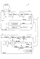
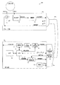
- FIG. 1 is a block diagram illustrating the configuration of the measurement apparatus according to the first embodiment.
- the measuring device 100 includes a main body 10, a probe 20, and a connection cable 30 that electrically connects the main body 10 and the probe 20 to each other.
- the main body unit 10 includes a CPU (Central Processing Unit) 11, a laser drive circuit 12, a power source 13, a display unit 14, a variable amplifier 15, an A / D converter 16, and an arithmetic unit 17. It is configured.
- CPU Central Processing Unit
- the main body unit 10 includes a CPU (Central Processing Unit) 11, a laser drive circuit 12, a power source 13, a display unit 14, a variable amplifier 15, an A / D converter 16, and an arithmetic unit 17. It is configured.
- CPU Central Processing Unit
- the probe unit 20 includes a light source 21 such as a semiconductor laser, a light receiving element 22, an amplifier 23, a reference voltage generator 24, and a nonvolatile memory 25 that stores predetermined probe data. Yes.
- connection cable 30 is formed integrally with the probe portion. At one end portion of the connection cable 30, a connector portion 31 formed to be detachable from the main body portion 10 is provided.
- the “non-volatile memory 25” includes “control means”, “drive current supply means”, “notification means”, “amplification means”, “calculation means”, “light receiving means”, “reference voltage generation” according to the present invention, respectively. It is an example of “means” and “storage means”.
- the power supply potential Vdd related to the power supply 13 of the main body 10 is supplied to the probe 20 via the connection cable 30.
- the power supply potential Vdd is supplied to, for example, the reference voltage generator 24.
- the reference voltage generator 24 generates a reference voltage according to the power supply potential Vdd.
- the generated reference voltage is applied to the laser drive circuit 12 of the main body 10 via the connection cable 30.
- FIG. 2 is a diagram illustrating an example of an electric circuit according to the reference voltage generator according to the first embodiment.
- the reference voltage generator 24 includes a Zener diode.
- a power supply potential Vdd is supplied to the cathode of the Zener diode.
- the anode of the Zener diode is connected to a ground (Gnd) line via a load resistor.
- the voltage between the cathode and anode of the Zener diode is a Zener voltage Vref defined by the characteristics of the Zener diode. Therefore, the anode potential of the Zener diode is “(power supply potential Vdd) ⁇ (zener voltage Vref)”.
- the potential of the anode is applied as a reference voltage to the laser drive circuit 12 of the main body 10 via the connection cable 30.
- the CPU 11 of the main body unit 10 acquires probe data (see FIG. 6) stored in advance in the nonvolatile memory 25 of the probe unit 20 via the connection cable 30.
- the CPU 11 controls the laser drive circuit 12 so that a predetermined drive current is output based on the laser drive adjustment value included in the acquired probe data.
- FIG. 3 is a diagram illustrating an example of an electric circuit according to the laser driving circuit according to the first embodiment.
- the laser drive circuit 12 matches the electronic volume for generating the adjustment voltage Vr for adjusting the drive current, the reference resistor R0, the adjustment voltage Vr, and the voltage drop V0 due to the reference resistor R0.
- Operational amplifier (OP amplifier) and a transistor for outputting a drive current are included in the laser drive circuit 12 .
- One end of the electronic volume is a power supply potential Vdd associated with the power supply 13, and the other end of the electronic volume is a reference voltage (ie, “(power supply potential Vdd) ⁇ (zener voltage Vref)”). Therefore, the voltage across the electronic volume is Vref.
- the electronic volume has a resolution of 6 bits, for example.
- the voltage between the electronic volume sweep terminal and the power supply potential Vdd (that is, the adjustment voltage Vr) is expressed by the following equation (1).
- Adjustment voltage Vr n ⁇ Vref / 63 (1)
- “n” is a laser drive adjustment value that is information for adjusting the drive current supplied to the light source 21, and the value is an integer of 0 to 63.
- the laser drive adjustment value is included in the acquired probe data and is designated by the CPU 11.
- the “laser drive adjustment value” according to the present embodiment is an example of “current adjustment information” according to the present invention.
- the sweep terminal of the electronic volume is connected to the + terminal of the operational amplifier.
- the collector current of the transistor is, for example, about two orders of magnitude larger than the base current.
- the power of emitted light required for the measuring apparatus 100 (“target light power” in FIG. 5 described later) is determined according to the measurement target of the measuring apparatus 100.
- a drive current If that satisfies the required output light power is obtained. It is determined.
- a Zener voltage Vref (that is, a Zener diode) that is smaller than the power supply potential Vdd is selected according to the power supply potential Vdd.
- the required output light power is 10 mW
- the drive current If that satisfies the required output light power is 25 mA
- the power supply potential Vdd is 10 V
- the Zener voltage is 5 V.
- the reference resistance R0 is determined from the drive current If and the Zener voltage Vref determined or selected in this way and the above equation (4).
- the laser drive adjustment value n may be set to 32, for example. As described above, when the drive current If is 25 mA and the Zener voltage is 5 V, the reference resistance R0 is 100 ⁇ .
- the measurement device 100 may be designed while appropriately selecting, for example, an element serving as the light source 21 and the power source 13 so that the values of the Zener voltage Vref, the reference resistance R0, and the like become appropriate values.
- the drive current If output from the laser drive circuit 12 is supplied to the light source 21 of the probe unit 20 via the connection cable 30.
- the light source 21 As a result, light is emitted from the light source 21 to the object to be measured (for example, blood flowing in the capillaries of the human body).
- the light receiving element 22 receives scattered light resulting from the emitted light (emitted light) and outputs a light reception signal.
- the emitted light is scattered by red blood cells (moving objects) in the blood.
- the frequency of light changes according to the moving speed of red blood cells.
- the emitted light is also scattered by non-moving objects such as skin tissue.
- Light scattered by red blood cells and light scattered by non-moving objects interfere with each other to generate an optical beat signal.
- the light receiving element 22 detects the optical beat signal and outputs it as a light receiving signal.
- the amplifier 23 of the probe unit 20 amplifies the light reception signal and outputs a light intensity signal which is the amplified light reception signal.
- the variable amplifier 15 of the main body 10 amplifies the light intensity signal so that the A / D converter 16 in the subsequent stage can appropriately perform A / D conversion.
- FIG. 4 is a diagram illustrating an example of an electric circuit according to the variable amplifier according to the first embodiment.
- the light intensity signal V1 output from the probe unit 20 is input to one end of the electronic volume.
- the other end of the electronic volume is set to a reference potential such as a ground potential.
- the sweep terminal of the electronic volume is connected to the non-inverting input terminal of the operational amplifier.
- One end of the input resistor R1 and one end of the feedback resistor Rf are connected to the inverting input terminal of the operational amplifier.
- the other end of the input resistor R0 is set to a reference potential such as a ground potential.
- the other end of the feedback resistor Rf is connected to the output terminal of the operational amplifier.
- the electronic volume has, for example, 6-bit resolution.
- the light intensity signal V1 output from the probe unit 20 is once attenuated according to the set value of the electronic volume, and is output as a signal V2 to the sweep terminal.
- the signal V2 is amplified by an operational amplifier and output as a signal V3.
- V2 (G1 / 63) V1 (5)
- G1 is a setting value of the electronic volume, and the value is, for example, an integer from 0 to 63.
- V3 / V2 1 + Rf / R1 (6)
- V3 (1 + Rf / R1)
- V2 (1 + Rf / R1) (G1 / 63) V1 (7) It becomes. That is, the light intensity signal V1 is amplified by the variable amplifier 15 according to the above equation (7).
- the light intensity signal V1 is amplified in proportion to the set value G1.
- Rf the feedback resistance
- Rf the input resistance
- the resistance has temperature characteristics, but the temperature characteristics of the resistance ratio can be ignored if they are placed close to the same substrate.
- the maximum resistance value of the electronic volume has a relatively large product variation, but the ratio between the sweep terminal and inter-terminal resistance (sweep resistance value) and the maximum resistance value is almost constant regardless of the product. Product variations can be ignored.
- the variation in the amplification factor shown by the above equation (7) is negligible.
- the light intensity signal V1 is amplified with an accurate amplification factor according to the set value G1, and is output as the signal V3.
- the A / D converter 16 A / D converts the amplified light intensity signal and outputs quantized data.
- the computing unit 17 performs a computation based on frequency analysis such as FFT (Fast Fourier Transform) on the output quantized data.
- FFT Fast Fourier Transform
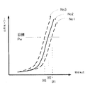
- FIG. 5 is a characteristic diagram showing an example of the IP characteristic of the semiconductor laser.
- the semiconductor laser having the characteristic corresponding to the broken line with the symbol “No1” outputs the emitted light of the target light power Pw when the drive current If1 is supplied.
- the semiconductor laser having the characteristic corresponding to the solid line with the symbol “No 2” outputs the emitted light of the target light power Pw when the driving current If2 smaller than the driving current If1 is supplied.
- the semiconductor laser having the characteristic corresponding to the broken line with the symbol “No 3” outputs the emitted light with the target light power Pw when the driving current If3 smaller than the driving current If2 is supplied.
- semiconductor lasers vary more or less among individuals even if the standards are the same. In other words, it is not possible to obtain emitted light having an appropriate optical power unless a driving current corresponding to the characteristics of the semiconductor laser is supplied.
- the power of the emitted light is lower than the target light power Pw, the power of the scattered light received by the light receiving element 22 is also reduced. Therefore, the S / N (Signal-Noise ratio) of the received light reception signal (and light intensity signal): Signal to noise ratio).
- the power of the emitted light is higher than the target light power Pw, there is a possibility that a problem occurs during measurement.
- probe data including a laser drive adjustment value is stored in advance in the nonvolatile memory 25 as described above. For this reason, even if the probe unit 20 of the measuring device 10 is replaced, the CPU 11 of the main body unit 10 uses the laser drive circuit 12 based on the probe data stored in advance in the nonvolatile memory 25 of the replaced probe unit 20.
- an appropriate driving current can be supplied to the light source 21. That is, when replacing the probe unit 20, it is not necessary to adjust the light source 21 by, for example, a serviceman.
- the user of the measuring apparatus 100 can replace the probe unit 20 relatively easily and in a short time.
- the cost can be greatly reduced as compared with the case where the measuring device 100 is replaced with a new one, which is very advantageous in practice.
- the probe unit 20 can be replaced in a relatively short time, it is not necessary to prepare a spare measuring device or the number of spare measuring devices can be reduced.
- FIG. 6 is an example of probe data stored in the nonvolatile memory according to the first embodiment.
- the probe data includes, for example, “management serial number” and “manufacturing date”, “laser drive adjustment value”, “variable amplifier adjustment value”, and probe unit 20 ( Here, “use time” and the like related to the light source 21) are included.
- variable amplifier adjustment value is an example of “amplification factor adjustment information” according to the present invention, and is information for adjusting the amplification factor related to the variable amplifier 15 of the main body 10.
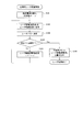
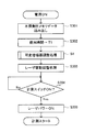
- the CPU 11 when a laser power adjustment process is requested for the CPU 11 of the main body 10 by an external input, the CPU 11 adjusts the laser drive adjustment in order to initialize the drive current supplied to the light source 21 of the probe unit 20.
- the CPU 11 commands the laser drive adjustment value n to the electronic volume (see FIG. 3) of the laser drive circuit 12 (step S102). As a result, a drive current is supplied from the laser drive circuit 12 to the light source 21 of the probe unit 20.
- the laser power of the laser light emitted from the light source 21 is measured by an optical power measuring instrument (not shown) installed outside, and the measurement result is transmitted to the CPU 11 of the main body 10 (step S103). Subsequently, the CPU 11 determines whether or not the measured laser power is equal to or higher than a target reference power (step S104).
- step S104 When it is determined that the measured laser power is equal to or higher than the reference power (step S104: Yes), the CPU 11 writes the current laser drive adjustment value n in the nonvolatile memory 25 of the probe unit 20 (step S106). The process ends.
- step S104 when it is determined that the measured laser power is less than the reference power (step S104: No), the CPU 11 resets the laser drive adjustment value n (step S105) and executes the process of step S102 again. .
- the laser drive circuit 12 generates a drive current by applying a reference voltage as described above (see, for example, FIGS. 1 and 3).
- the reference voltage is determined by the Zener diode (see FIG. 2) of the reference voltage generator 24.
- Zener diodes have individual variations of about ⁇ several percent. If the probe unit 20 is replaced when the main body unit 10 includes the reference voltage generator 24, the reference voltage becomes the reference voltage when the laser drive adjustment value is set due to the individual variation of the Zener diodes. May change. Then, even if the laser drive adjustment value is set at the time of shipment as described above, an appropriate drive current may not be supplied to the light source 21 depending on the main body unit 10 to which the probe unit 20 is electrically connected.
- the reference voltage generator 24 is provided in the probe unit 20 as described above. Therefore, even if the probe unit 20 is replaced, the reference voltage can be kept the same as the reference voltage when the laser drive adjustment value is set. That is, by providing the probe unit 20 with the reference voltage generator 24, it is possible to suppress variations in drive current due to individual variations in the Zener diodes that constitute the reference voltage generator 24.
- variable amplifier adjustment value For example, laser light emitted from the light source 21 due to individual variations of the probe unit 20 due to variations in sensitivity of the light receiving elements 22, displacement of the light receiving elements 22, displacement of lenses (not shown), displacement of the light sources 21, etc. Even if the power of the light is constant, the light intensity signal (see FIG. 1) from the probe unit 20 changes (for example, amplitude fluctuation).
- the A / D conversion is performed without correcting the fluctuation in the amplitude of the light intensity signal, the following problems may occur. That is, if the amplitude of the light intensity signal is too small, the amount of amplitude is insufficient with respect to the input D range of the A / D converter 16, resulting in a quantization error and a large error in subsequent calculations. On the other hand, when the amplitude of the light intensity signal is too large, the input D range of the A / D converter 16 is exceeded, so that the quantized data is saturated and the signal is distorted, so that a large error occurs in the subsequent calculation. .
- variable amplifier adjustment value is stored in advance in the nonvolatile memory 25 of the probe unit 20 so that the user can replace the probe unit 20 relatively easily.
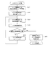
- the laser beam is emitted from the light source 21 while maintaining an appropriate optical arrangement on a reflector (not shown) having a predetermined reflectance. Is irradiated (step S201).
- the CPU 11 of the main body 10 initializes the variable amplifier adjustment value and stores it in a register inside the CPU 11 (step S202).
- the CPU 11 commands the variable amplifier adjustment value G1 to the electronic volume (see FIG. 4) of the variable amplifier 15 (step S203).
- the CPU 11 acquires an A / D conversion value related to the A / D converter 16 (step S204). Subsequently, the CPU 11 determines whether or not the acquired A / D conversion value is equal to or more than a target reference A / D value (step S205).
- the “reference A / D value” is output from the probe unit 20 when, for example, scattered light is received when laser light having a prescribed laser power is applied to a reflector having a predetermined reflectance.
- a typical light intensity signal may be set as an A / D conversion value when input to the A / D converter 16.
- a center value (for example, 32) is set as the variable amplifier adjustment value G1.
- step S205 When it is determined that the acquired A / D conversion value is greater than or equal to the reference A / D value (step S205: Yes), the CPU 11 stores the current variable amplifier adjustment value G1 in the nonvolatile memory 25 of the probe unit 20. Writing (step S207) and the process is terminated.
- step S205 when it is determined that the acquired A / D conversion value is less than the reference A / D value (step S205: No), the CPU 11 resets the variable amplifier adjustment value G1 (step S206), and step S203. The above process is executed again.
- the light intensity signal is amplified with an accurate amplification factor according to the set value G1, and is output as the signal V3 (see FIG. 4). Therefore, referring to the variable amplifier adjustment value G1 stored in the nonvolatile memory 25, the amplitude level suitable for the input D range of the A / D converter 16 is maintained even if the probe unit 20 is replaced.
- the signal V3 having an appropriate amplitude is input to the A / D converter 16, an increase in quantization error at a low amplitude can be suppressed, and a signal distortion due to saturation at a high amplitude can be suppressed. .
- the CPU 11 of the main body unit 10 reads the probe data stored in the nonvolatile memory 25 of the probe unit 20 (step S301). Subsequently, the CPU 11 stores the counter value T1 in a register inside the CPU 11 based on the usage time included in the probe data (step S302).
- the “use time” according to the present embodiment means the total lighting time of the light source 21. For example, when the usage time is 100 hours, the counter value T1 is “100”.
- step S4 the CPU 11 controls the variable amplifier 16 based on the variable amplifier adjustment value included in the probe data.
- step S4 the processing of step S4 will be described with reference to the flowchart of FIG.
- the CPU 11 after reading the probe data stored in the non-volatile memory 25 of the probe unit 20 (step S401), the CPU 11 relates to the variable amplifier 15 based on the variable amplifier adjustment value included in the probe data.
- the set value is set to “G1” (step S402). Subsequently, the CPU 11 sets G1 in the electronic volume of the variable amplifier 15 (step S403).
- step S4 the CPU 11 controls the laser drive circuit 12 based on the laser drive adjustment value included in the probe data (step S303). Subsequently, the CPU 11 determines whether or not a measurement switch (not shown) of the measurement device 100 is turned on (step S304).
- step S304: No When it is determined that the measurement switch is not in the ON state (that is, in the OFF state) (step S304: No), the CPU 11 executes the process of step S304 again (that is, enters a standby state). On the other hand, when it is determined that the measurement switch is turned on (step S304: Yes), the CPU 11 controls the laser drive circuit 12 to supply a drive current to the light source 21 of the probe unit 20 (step S305).
- the CPU 11 clears the 1-hour timer flag and starts a timer program (step S501).
- the timer program is configured to set a one hour timer flag after one hour has elapsed.
- step S502 determines whether or not the value of the one-hour timer flag is “1” (that is, one hour has elapsed) (step S502).
- step S502: No the CPU 11 executes the process of step S502 again.
- step S503 the CPU 11 increments the counter value T1 and stores it in a register inside the CPU 11 (step S503).
- the CPU 11 determines whether or not the counter value T1 exceeds a specified value T1over which is, for example, 500 hours (step S504).
- a specified value T1over which is, for example, 500 hours
- the CPU 11 executes a process of step S506 described later.
- the CPU 11 displays, for example, a warning indicating that the usage time is exceeded on the display unit 14 (step S505).
- step S506 determines whether or not the measurement switch of the measurement apparatus 100 has been turned off.
- step S506: No the CPU 11 executes the process of step S501.
- step S506 determines that the measurement switch has been turned off.
- the CPU 11 controls the laser drive circuit 12 so as not to supply a drive current to the light source 21 of the probe unit 20 (step S507).
- the CPU 11 writes the counter value T1 as a usage time (step S508) and writes it in the nonvolatile memory 25 of the probe unit 20 (step S509).
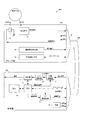
- FIG. 12 is a block diagram illustrating the configuration of the measurement apparatus according to the second embodiment.
- the measuring apparatus 200 includes a main body unit 10, a probe unit 20a, and a connection cable 30a that electrically connects the main body unit 10 and the probe unit 20a.
- the connection cable 30a is formed integrally with the probe portion 20a.
- a nonvolatile memory 35 for storing probe data and a reference voltage generator 34 are built in the connector portion 31a of the connection cable 30a. If comprised in this way, since the probe part 20a can be reduced in size and weight, it is very advantageous practically.
- FIG. 13 is a block diagram illustrating the configuration of the measurement apparatus according to the third embodiment.
- the measuring apparatus 300 includes a main body portion 10b, a probe portion 20b, and a connection cable 30b that electrically connects the main body portion 10b and the probe portion 20b.
- the connection cable 30b is formed integrally with the main body 10b.
- the connector part 32 of the connection cable 30b is formed to be detachable from the probe part 20b.
- a light emitting diode (LED) is used as the light source 21 of the probe unit 20b.
- the light reception signal output from the light receiving element 22 of the probe unit 20b is transmitted to the variable amplifier 15 of the main body unit 10b via the connection cable 30b.
- the main body 10b is configured to include an LED drive circuit 12a in response to the use of a light emitting diode as the light source 21 of the probe 20b.
- the computing unit 17 of the main body 10b estimates the blood concentration from the intensity change of the data quantized by the A / D converter 16. It should be noted that various known modes can be applied to the blood concentration estimation method, and therefore, detailed description thereof is omitted.
- a semiconductor laser can be used instead of the light emitting diode.
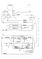
- FIG. 14 is a block diagram illustrating the configuration of the measurement apparatus according to the fourth example.
- the measuring apparatus 400 includes a main body 10c, a probe 20c, and a connection cable 30c that electrically connects the main body 10c and the probe 20c.
- the connection cable 30c is formed integrally with the main body 10c.
- the connector part 32 of the connection cable 30c is formed to be detachable from the probe part 20c.
- the probe 20c includes two light sources 21 and 26. As the light sources 21 and 26, light emitting diodes having different wavelengths are used.
- the light reception signal output from the light receiving element 22 of the probe unit 20c is transmitted to the variable amplifier 15 of the main body unit 10c via the connection cable 30c.
- the probe data stored in the nonvolatile memory 25 includes a laser drive adjustment value corresponding to the light source 21 and a laser drive adjustment value corresponding to the light source 26.
- the main body 10c includes an LED drive circuit 12b in response to the use of light emitting diodes for the light sources 21 and 26 of the probe 20c.
- the LED drive circuit 12 b is configured to be able to output a drive current 1 for driving the light source 21 and a drive current 2 for driving the light source 26. Further, the CPU 11 controls the LED drive circuit 12 b based on both the laser drive adjustment value corresponding to the light source 21 and the laser drive adjustment value corresponding to the light source 26.
- the computing unit 17 of the main body 10c estimates the oxygen saturation in the blood from the intensity change of the data quantized by the A / D converter 16. In addition, since various well-known aspects are applicable to the estimation method of the oxygen saturation in blood, the description about the detail is omitted.
- the present invention is not limited to the above-described embodiment, and can be appropriately changed without departing from the gist or concept of the invention that can be read from the claims and the entire specification. And the connecting cable are also included in the technical scope of the present invention.
Abstract
Description
実施形態に係る第1の計測装置は、相互に電気的に接続されたプローブ部及び本体部を備える光学式の計測装置であって、前記プローブ部は、光源と、前記本体部に対して所定の基準電圧を印加する基準電圧発生手段と、前記光源に供給される駆動電流を調整するための情報である電流調整情報を予め格納する記憶手段と、を有し、前記本体部は、前記印加された基準電圧に起因して、前記光源に対して前記駆動電流を供給可能な駆動電流供給手段と、前記格納された電流調整情報に基づいて、前記光源に供給すべき駆動電流値となるように前記駆動電流供給手段を制御する制御手段と、を有する。
実施形態に係るプローブ部は、光学式の計測装置の本体部に電気的に接続され、前記本体部からの駆動電流が供給されるプローブ部であって、前記駆動電流に起因して光を出射する光源と、前記本体部に対して、前記駆動電流を生成させるための所定の基準電圧を印加する基準電圧発生手段と、前記本体部において、前記駆動電流を調整するための情報である電流調整情報を予め格納する記憶手段と、を備える。
実施形態に係る接続ケーブルは、光源を有するプローブ部と、前記光源に対して駆動電流を供給可能な駆動電流供給手段、及び前記駆動電流供給手段を制御する制御手段を有する本体部と、を備える光学式の計測装置において、前記プローブ部及び前記本体部を相互に電気的に接続する接続ケーブルであって、前記プローブ部又は前記本体部に着脱可能なコネクタ部を備え、前記コネクタ部は、前記本体部に対して、前記駆動電流供給手段に前記駆動電流を生成させるための所定の基準電圧を印加する基準電圧発生手段と、前記制御手段が前記駆動電流を調整するための情報である電流調整情報を予め格納する記憶手段と、を有する。
本発明の計測装置に係る第1実施例を、図面に基づいて説明する。
調整電圧Vr=n・Vref/63・・・・・(1)
ここで、“n”は、光源21に供給される駆動電流を調整するための情報であるレーザ駆動調整値であり、その値は0~63の整数である。該レーザ駆動調整値は、上述の如く、取得されたプローブデータに含まれており、CPU11により指定される。尚、本実施例に係る「レーザ駆動調整値」は、本発明に係る「電流調整情報」の一例である。
(調整電位Vr)=(基準抵抗R0による電圧降下V0)・・・・・(2)
となる。
駆動電流If=V0/R0・・・・・(3)
となる。
駆動電流If=Vr/R0=n・Vref/(63・R0)・・・・・(4)
となる。
上記式(4)からわかるように、基準抵抗R0が一定であれば、駆動電流Ifは“n・Vref”に比例する。このため、CPU11がレーザ駆動調整値nを指定することにより駆動電流Ifを制御することができる。
V2=(G1/63)V1・・・・・(5)
ここで、“G1”は、電子ボリュームの設定値であり、その値は、例えば0~63の整数である。
V3/V2=1+Rf/R1・・・・・(6)
上記式(5)及び(6)から、
V3=(1+Rf/R1)V2=(1+Rf/R1)(G1/63)V1・・・・・(7)
となる。つまり、光強度信号V1は、上記式(7)に従って、可変増幅器15により増幅される。
次に、出荷時におけるレーザ駆動調整値の設定方法について、図7のフローチャートを参照して説明する。
次に、計測装置100の計測時における処理について、図9乃至図11のフローチャートを参照して説明する。
本発明の計測装置に係る第2実施例を、図12を参照して説明する。尚、第2実施例では、プローブ部及び接続ケーブルの構成が一部異なっている以外は、第1実施例と同じであるので、重複する説明を省略すると共に、図面上の同一箇所には同一符号を付して示し、基本的に、第1実施例と異なる部分についてのみ、図12を参照して説明する。図12は、第2実施例に係る計測装置の構成を示すブロック図である。
本発明の計測装置に係る第3実施例を、図13を参照して説明する。尚、第3実施例では、計測装置の構成が一部異なっている以外は、第1実施例と同じであるので、重複する説明を省略すると共に、図面上の同一箇所には同一符号を付して示し、基本的に、第1実施例と異なる部分についてのみ、図13を参照して説明する。図13は、第3実施例に係る計測装置の構成を示すブロック図である。
本発明の計測装置に係る第4実施例を、図14を参照して説明する。尚、第4実施例では、計測装置の構成が一部異なっている以外は、第1実施例と同じであるので、重複する説明を省略すると共に、図面上の同一箇所には同一符号を付して示し、基本的に、第1実施例と異なる部分についてのみ、図14を参照して説明する。図14は、第4実施例に係る計測装置の構成を示すブロック図である。
Claims (10)
- 相互に電気的に接続されたプローブ部及び本体部を備える光学式の計測装置であって、
前記プローブ部は、
光源と、
前記本体部に対して所定の基準電圧を印加する基準電圧発生手段と、
前記光源に供給される駆動電流を調整するための情報である電流調整情報を予め格納する記憶手段と、
を有し、
前記本体部は、
前記印加された基準電圧に起因して、前記光源に対して前記駆動電流を供給可能な駆動電流供給手段と、
前記格納された電流調整情報に基づいて、前記光源に供給すべき駆動電流値となるように前記駆動電流供給手段を制御する制御手段と、
を有する
ことを特徴とする計測装置。 - 相互に電気的に接続されたプローブ部及び本体部を備える光学式の計測装置であって、
前記プローブ部は、
光源と、
前記本体部に対して所定の基準電圧を印加する基準電圧発生手段と、
前記光源に供給される駆動電流を調整するための情報である電流調整情報を予め格納する記憶手段と、
前記光源から出射された光の対象物からの散乱光を受光して、受光信号を出力する受光手段と、
を有し、
前記本体部は、
前記印加された基準電圧に起因して、前記光源に対して前記駆動電流を供給可能な駆動電流供給手段と、
前記格納された電流調整情報に基づいて、前記光源に供給すべき駆動電流値となるように前記駆動電流供給手段を制御する制御手段と、
前記出力された受光信号に基づいて前記対象物に係る状態量を演算する演算手段と、
を有する
ことを特徴とする計測装置。 - 前記記憶手段は、前記プローブ部の使用時間を示す情報である使用時間情報を更に格納することを特徴とする請求項1又は2に記載の計測装置。
- 前記制御手段は、当該計測装置の動作時間に応じて、前記使用時間情報を更新することを特徴とする請求項3に記載の計測装置。
- 前記本体部は、前記格納された使用時間情報により示される使用時間が所定値より大きい場合に、当該計測装置のユーザに対して報知する報知手段を更に有することを特徴とする請求項3に記載の計測装置。
- 前記本体部は、前記出力された受光信号を増幅率可変に増幅する増幅手段を更に有し、
前記記憶手段は、前記増幅手段に係る増幅率を調整するための情報である増幅率調整情報を更に格納する
ことを特徴とする請求項2に記載の計測装置。 - 前記制御手段は、前記格納された増幅率調整情報に基づいて、前記増幅手段を制御することを特徴とする請求項5に記載の計測装置。
- 当該計測装置は、血流検出装置であることを特徴とする請求項1又は2に記載の計測装置。
- 光学式の計測装置の本体部に電気的に接続され、前記本体部からの駆動電流が供給されるプローブ部であって、
前記駆動電流に起因して光を出射する光源と、
前記本体部に対して、前記駆動電流を生成させるための所定の基準電圧を印加する基準電圧発生手段と、
前記本体部において、前記駆動電流を調整するための情報である電流調整情報を予め格納する記憶手段と、
を備えることを特徴とするプローブ部。 - 光源を有するプローブ部と、前記光源に対して駆動電流を供給可能な駆動電流供給手段、及び前記駆動電流供給手段を制御する制御手段を有する本体部と、を備える光学式の計測装置において、前記プローブ部及び前記本体部を相互に電気的に接続する接続ケーブルであって、
前記プローブ部又は前記本体部に着脱可能なコネクタ部を備え、
前記コネクタ部は、
前記本体部に対して、前記駆動電流供給手段に前記駆動電流を生成させるための所定の基準電圧を印加する基準電圧発生手段と、
前記制御手段が前記駆動電流を調整するための情報である電流調整情報を予め格納する記憶手段と、
を有する
ことを特徴とする接続ケーブル。
Priority Applications (4)
| Application Number | Priority Date | Filing Date | Title |
|---|---|---|---|
| US14/648,766 US10070797B2 (en) | 2012-12-05 | 2012-12-05 | Measuring apparatus, probe portion, and connecting cable |
| EP12889536.4A EP2929834A4 (en) | 2012-12-05 | 2012-12-05 | MEASURING DEVICE, SONDENTEIL AND CONNECTING CABLE |
| PCT/JP2012/081519 WO2014087502A1 (ja) | 2012-12-05 | 2012-12-05 | 計測装置、プローブ部及び接続ケーブル |
| JP2014550847A JP6082027B2 (ja) | 2012-12-05 | 2012-12-05 | 計測装置、プローブ部及び接続ケーブル |
Applications Claiming Priority (1)
| Application Number | Priority Date | Filing Date | Title |
|---|---|---|---|
| PCT/JP2012/081519 WO2014087502A1 (ja) | 2012-12-05 | 2012-12-05 | 計測装置、プローブ部及び接続ケーブル |
Publications (1)
| Publication Number | Publication Date |
|---|---|
| WO2014087502A1 true WO2014087502A1 (ja) | 2014-06-12 |
Family
ID=50882952
Family Applications (1)
| Application Number | Title | Priority Date | Filing Date |
|---|---|---|---|
| PCT/JP2012/081519 WO2014087502A1 (ja) | 2012-12-05 | 2012-12-05 | 計測装置、プローブ部及び接続ケーブル |
Country Status (4)
| Country | Link |
|---|---|
| US (1) | US10070797B2 (ja) |
| EP (1) | EP2929834A4 (ja) |
| JP (1) | JP6082027B2 (ja) |
| WO (1) | WO2014087502A1 (ja) |
Cited By (1)
| Publication number | Priority date | Publication date | Assignee | Title |
|---|---|---|---|---|
| JP2017080517A (ja) * | 2017-01-19 | 2017-05-18 | パイオニア株式会社 | 計測装置、プローブ部及び接続ケーブル |
Families Citing this family (3)
| Publication number | Priority date | Publication date | Assignee | Title |
|---|---|---|---|---|
| JP6597410B2 (ja) * | 2016-03-04 | 2019-10-30 | セイコーエプソン株式会社 | 生体情報測定装置および生体情報測定方法 |
| EP3550270B1 (en) * | 2016-11-29 | 2022-01-05 | Pioneer Corporation | Measurement device |
| JP6983093B2 (ja) * | 2018-03-27 | 2021-12-17 | 日東電工株式会社 | 抵抗測定装置、フィルム製造装置および導電性フィルムの製造方法 |
Citations (5)
| Publication number | Priority date | Publication date | Assignee | Title |
|---|---|---|---|---|
| JP3490433B1 (ja) | 2003-06-02 | 2004-01-26 | 株式会社サイバーファーム | 生体情報監視システム |
| WO2005099575A1 (ja) * | 2004-04-15 | 2005-10-27 | Moritex Corporation | 顔面撮像装置 |
| WO2006064635A1 (ja) * | 2004-12-17 | 2006-06-22 | Konica Minolta Holdings, Inc. | 診断システム |
| WO2010023744A1 (ja) * | 2008-08-28 | 2010-03-04 | パイオニア株式会社 | 生体情報測定装置 |
| JP4460566B2 (ja) | 2006-12-07 | 2010-05-12 | 日本電信電話株式会社 | 光学センサ及び生体情報測定装置 |
Family Cites Families (5)
| Publication number | Priority date | Publication date | Assignee | Title |
|---|---|---|---|---|
| US6515273B2 (en) | 1999-08-26 | 2003-02-04 | Masimo Corporation | System for indicating the expiration of the useful operating life of a pulse oximetry sensor |
| JP3688544B2 (ja) | 1999-12-27 | 2005-08-31 | 横河電機株式会社 | 測定信号出力装置 |
| US9408538B2 (en) * | 2006-05-03 | 2016-08-09 | Triple Ring Technologies, Inc. | Method and apparatus for pressure sore detection |
| WO2009134724A1 (en) | 2008-05-02 | 2009-11-05 | Masimo Corporation | Monitor configuration system |
| EP2586366B1 (en) | 2010-06-24 | 2016-04-06 | Pioneer Corporation | Photo-detection device and fluid measurement device |
-
2012
- 2012-12-05 US US14/648,766 patent/US10070797B2/en active Active
- 2012-12-05 WO PCT/JP2012/081519 patent/WO2014087502A1/ja active Application Filing
- 2012-12-05 JP JP2014550847A patent/JP6082027B2/ja active Active
- 2012-12-05 EP EP12889536.4A patent/EP2929834A4/en not_active Withdrawn
Patent Citations (5)
| Publication number | Priority date | Publication date | Assignee | Title |
|---|---|---|---|---|
| JP3490433B1 (ja) | 2003-06-02 | 2004-01-26 | 株式会社サイバーファーム | 生体情報監視システム |
| WO2005099575A1 (ja) * | 2004-04-15 | 2005-10-27 | Moritex Corporation | 顔面撮像装置 |
| WO2006064635A1 (ja) * | 2004-12-17 | 2006-06-22 | Konica Minolta Holdings, Inc. | 診断システム |
| JP4460566B2 (ja) | 2006-12-07 | 2010-05-12 | 日本電信電話株式会社 | 光学センサ及び生体情報測定装置 |
| WO2010023744A1 (ja) * | 2008-08-28 | 2010-03-04 | パイオニア株式会社 | 生体情報測定装置 |
Non-Patent Citations (1)
| Title |
|---|
| See also references of EP2929834A4 * |
Cited By (1)
| Publication number | Priority date | Publication date | Assignee | Title |
|---|---|---|---|---|
| JP2017080517A (ja) * | 2017-01-19 | 2017-05-18 | パイオニア株式会社 | 計測装置、プローブ部及び接続ケーブル |
Also Published As
| Publication number | Publication date |
|---|---|
| JPWO2014087502A1 (ja) | 2017-01-05 |
| US10070797B2 (en) | 2018-09-11 |
| US20150327782A1 (en) | 2015-11-19 |
| EP2929834A4 (en) | 2016-08-03 |
| EP2929834A1 (en) | 2015-10-14 |
| JP6082027B2 (ja) | 2017-02-15 |
Similar Documents
| Publication | Publication Date | Title |
|---|---|---|
| JP6082027B2 (ja) | 計測装置、プローブ部及び接続ケーブル | |
| JP2008505342A (ja) | 赤外線放射源調整法及びその調整法を使用する装置 | |
| JP5884251B2 (ja) | 光データリンクの製造方法 | |
| TW201244526A (en) | Optical power compensation circuit and device, and detecting module | |
| KR20170048584A (ko) | 액티브 소자의 잔여 수명을 근사하는 방법 | |
| JP2017080517A (ja) | 計測装置、プローブ部及び接続ケーブル | |
| TWI247464B (en) | Method and apparatus for measuring bandwidth of an optical spectrum output of a very small wavelength very narrow bandwidth high power laser | |
| JP2009020101A (ja) | コリオリ型流量計 | |
| WO2020217355A1 (ja) | 劣化診断装置および光トランシーバの劣化診断方法 | |
| CN104730308A (zh) | 控制电光探针增益和灵敏度的方法 | |
| JP2007516417A5 (ja) | ||
| JP4770916B2 (ja) | 電子値札システム | |
| JP5488159B2 (ja) | 定電力制御回路 | |
| JP4651471B2 (ja) | 半導体レーザ装置 | |
| JP2009239032A (ja) | レーザダイオード駆動回路およびレーザ溶着電源 | |
| TWI381183B (zh) | 判斷交流/直流交叉校正係數之系統和方法 | |
| JP2021190510A (ja) | 光量調整装置、光量調整システム及び光量調整方法 | |
| JP2006302967A (ja) | 光モジュール | |
| WO2023181582A1 (ja) | センサシステム | |
| KR102123087B1 (ko) | 실시간 서버 모니터링 시스템 | |
| US11381055B2 (en) | Laser system | |
| JP6321461B2 (ja) | 半導体光装置、及び制御方法 | |
| US20230337926A1 (en) | Measurement device, measurement system, measurement method, and non-transitory computer-readable recording medium | |
| KR910008654B1 (ko) | 혈당측정기의 측정오차 보상방법 및 광원조절회로 | |
| JP6963488B2 (ja) | 温度計測装置 |
Legal Events
| Date | Code | Title | Description |
|---|---|---|---|
| 121 | Ep: the epo has been informed by wipo that ep was designated in this application |
Ref document number: 12889536 Country of ref document: EP Kind code of ref document: A1 |
|
| ENP | Entry into the national phase |
Ref document number: 2014550847 Country of ref document: JP Kind code of ref document: A |
|
| WWE | Wipo information: entry into national phase |
Ref document number: 2012889536 Country of ref document: EP |
|
| WWE | Wipo information: entry into national phase |
Ref document number: 14648766 Country of ref document: US |
|
| NENP | Non-entry into the national phase |
Ref country code: DE |