WO2014080668A1 - 高周波増幅回路 - Google Patents
高周波増幅回路 Download PDFInfo
- Publication number
- WO2014080668A1 WO2014080668A1 PCT/JP2013/070842 JP2013070842W WO2014080668A1 WO 2014080668 A1 WO2014080668 A1 WO 2014080668A1 JP 2013070842 W JP2013070842 W JP 2013070842W WO 2014080668 A1 WO2014080668 A1 WO 2014080668A1
- Authority
- WO
- WIPO (PCT)
- Prior art keywords
- circuit
- field effect
- voltage
- fet
- effect transistor
- Prior art date
- Legal status (The legal status is an assumption and is not a legal conclusion. Google has not performed a legal analysis and makes no representation as to the accuracy of the status listed.)
- Ceased
Links
Images







Classifications
-
- H—ELECTRICITY
- H03—ELECTRONIC CIRCUITRY
- H03F—AMPLIFIERS
- H03F1/00—Details of amplifiers with only discharge tubes, only semiconductor devices or only unspecified devices as amplifying elements
- H03F1/30—Modifications of amplifiers to reduce influence of variations of temperature or supply voltage or other physical parameters
- H03F1/301—Modifications of amplifiers to reduce influence of variations of temperature or supply voltage or other physical parameters in MOSFET amplifiers
-
- H—ELECTRICITY
- H03—ELECTRONIC CIRCUITRY
- H03F—AMPLIFIERS
- H03F3/00—Amplifiers with only discharge tubes or only semiconductor devices as amplifying elements
- H03F3/189—High-frequency amplifiers, e.g. radio frequency amplifiers
- H03F3/19—High-frequency amplifiers, e.g. radio frequency amplifiers with semiconductor devices only
- H03F3/193—High-frequency amplifiers, e.g. radio frequency amplifiers with semiconductor devices only with field-effect devices
-
- H—ELECTRICITY
- H03—ELECTRONIC CIRCUITRY
- H03F—AMPLIFIERS
- H03F2200/00—Indexing scheme relating to amplifiers
- H03F2200/15—Indexing scheme relating to amplifiers the supply or bias voltage or current at the drain side of a FET being continuously controlled by a controlling signal
-
- H—ELECTRICITY
- H03—ELECTRONIC CIRCUITRY
- H03F—AMPLIFIERS
- H03F2200/00—Indexing scheme relating to amplifiers
- H03F2200/18—Indexing scheme relating to amplifiers the bias of the gate of a FET being controlled by a control signal
Definitions
- the present invention relates to a high-frequency amplifier circuit that amplifies and outputs an input high-frequency signal, and more particularly, to a high-frequency amplifier circuit that uses an enhancement type field effect transistor as an amplifying element.
- a transmission circuit of a communication device is provided with a high-frequency amplifier circuit that amplifies a high-frequency signal used for communication.
- a high-frequency amplifier circuit for example, a field effect transistor (hereinafter referred to as “FET”) for amplifying a high-frequency signal is used as shown in FIG.
- FET field effect transistor
- the gate bias voltage of the high frequency amplification FET is applied through a resistor.
- Patent Document 1 it is known that the drain current varies due to manufacturing variations of the high frequency amplification FET, and the high frequency amplification circuit described in Patent Document 1 has the following configuration.
- the gate of the high frequency amplification FET is provided with a gate bias circuit including a compensation FET having the same structure as the high frequency amplification FET.
- the gate bias circuit has a configuration in which a compensation FET and two resistors are cascaded between a gate bias (-VGG) application terminal and a ground. Specifically, a resistor, a compensation FET, and a resistor are connected from the gate bias ( ⁇ VGG) application terminal side. Each resistor is connected to the drain and source of the compensation FET.
- a gate bias ( ⁇ VGG) is directly applied to the gate of the compensation FET.
- the pinch off voltage of the compensation FET when the pinch-off voltage of the high frequency amplification FET deviates from the design value, the pinch off voltage of the compensation FET similarly deviates from the design value. Due to the deviation of the pinch-off voltage of the compensation FET, the output voltage of the gate bias circuit (the gate bias voltage of the high-frequency amplification FET) changes so as to compensate for the deviation of the pinch-off voltage.
- the high-frequency amplification FET and the compensation FET described in Patent Document 1 having such a configuration are composed of a depletion-side FET.
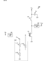
- FIG. 13 is a circuit diagram of a conventional high-frequency amplifier circuit.
- the high frequency amplifier circuit 10P includes a field effect transistor 101 (FET 101) for high frequency amplification.
- the FET 101 is an enhancement type.
- the high frequency signal input terminal Pin is connected to the gate of the FET 101 through the input matching circuit 901.
- Gate bias voltage setting circuit 110P is series-connected resistors 211P between the gate bias voltage application terminal P VG and the ground, and a 212P.
- the connection point of the resistors 211P and 212P is connected to the gate of the FET 101 via the resistor 213P.
- the gate bias voltage of the FET 101 is changed by changing the resistance ratio of the resistors 211P and 212P, and the drain current of the FET 101, that is, the output power of the high-frequency amplifier circuit 10P is adjusted.
- Patent Document 1 uses a depletion type FET for each FET. Therefore, Patent Document 1 does not describe a method for suppressing variation in drain current due to manufacturing variations of a high-frequency amplification FET in a high-frequency amplification circuit with respect to a case where an enhancement type FET is used.
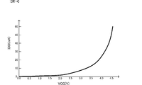
- FIG. 14 is a characteristic diagram showing the relationship between the gate bias voltage and the drain current of a conventional high-frequency amplifier circuit.
- FIG. 15 is a characteristic diagram showing the relationship between the fluctuation of the pinch-off voltage and the drain current when the gate bias voltage is fixed in the conventional high-frequency amplifier circuit.
- the relationship between the gate bias voltage V GG and the drain current I DD is non-linear, and when the gate bias voltage V GG exceeds a predetermined value, the drain current I DD increases.
- the gate bias voltage VGG in a region where the drain current IDD is nonlinear and changes rapidly must be used.
- the amount of change in the drain current IDD according to the change in the gate bias voltage VGG is large, and it is difficult to stably obtain the target output power.
- the variation of the drain current I DD in accordance with the fluctuation amount of the pinch-off voltage of the FET for high frequency amplification is also non-linear.
- the drain current IDD increases rapidly even when the base bias voltage is the same as compared to when the pinch-off voltage is high.
- An object of the present invention is to provide a high-frequency amplifier circuit that can obtain stable output power even if the gate bias voltage VGG and the pinch-off voltage of the high-frequency amplifier FET vary.
- the present invention relates to a high-frequency amplifier circuit including a field-effect transistor for high-frequency amplification and a gate bias voltage setting circuit that determines the gate bias of the field-effect transistor, and has the following characteristics.
- the field effect transistor for high frequency amplification is an enhancement type.
- the gate bias voltage setting circuit includes a constant voltage circuit that outputs a predetermined voltage in a state where an input gate bias voltage VGG input from the outside is applied, and a voltage compensation circuit having a plurality of enhancement type field effect transistors for compensation.
- the plurality of compensation field effect transistors include a first compensation field effect transistor to which a voltage input from a constant voltage circuit is applied, and a drain current between the drain and source due to an increase in drain current of the first compensation field effect transistor.
- the second compensation field effect transistor has a second on-resistance that decreases on-resistance and increases on-resistance between the drain and source due to a decrease in drain current of the first compensation field-effect transistor.
- the gate bias voltage of the field effect transistor for high frequency amplification is adjusted to The drain current of the field effect transistor is kept constant.
- the gate bias voltage of the field effect transistor for high frequency amplification is adjusted and the drain of the field effect transistor for high frequency amplification is adjusted. The current is kept constant.
- the high frequency amplifier circuit of the present invention may have the following configuration.
- the second compensation field effect transistor is grounded at the source.
- Two resistors are connected in series between the source of the first compensating field effect transistor and the drain of the second compensating field effect transistor.
- the gate of the second compensation field effect transistor is connected to the connection point of the two resistors.
- the drain of the second compensation field effect transistor is connected to the gate of the field effect transistor for high frequency amplification.
- This configuration shows a specific circuit configuration example of the voltage compensation circuit.
- the drain of the first compensation field effect transistor is connected to the same drive voltage application terminal as the drain of the field effect transistor for high frequency amplification.
- the current that can be applied to the gate of the field effect transistor for high frequency amplification can be increased.
- the resistor connected in series to the gate of the field effect transistor for high frequency amplification has a low resistance, a large current can be supplied to the gate. Therefore, the output characteristics of the high frequency amplifier circuit can be improved.
- a high-impedance circuit having high impedance for a high-frequency signal is connected between the drain of the first compensation field-effect transistor and the drain of the field-effect transistor for high-frequency amplification. It is preferable that
- the high impedance circuit of the high frequency amplifier circuit of the present invention may be a resistor.
- the high impedance circuit of the high frequency amplifier circuit of the present invention may be a coil.
- the high impedance circuit of the high frequency amplifier circuit of the present invention may be a parallel resonance circuit of a coil and a capacitor whose resonance frequency is the frequency of the high frequency signal.
- the constant voltage circuit of the high frequency amplifier circuit of the present invention includes a plurality of enhancement type field effect transistors for constant voltage, and each of the plurality of constant voltage field effect transistors is diode-connected and cascade-connected. Preferably it is.
- This configuration shows a specific configuration example of the constant voltage circuit.
- the constant voltage circuit has the same fluctuation characteristics as the pinch-off voltage of the field effect transistor for high frequency amplification.
- the voltage also changes. Therefore, it is possible to generate an appropriate and stable voltage corresponding to the pinch-off voltage of the field effect transistor for high frequency amplification.
- the constant voltage circuit of the high-frequency amplifier circuit of the present invention may include a plurality of n-type bipolar transistors, and each of the plurality of n-type bipolar transistors may be diode-connected and cascade-connected.
- This configuration shows a case where the constant voltage circuit is configured by a bipolar transistor. Even with such a bipolar transistor, a constant voltage circuit can be configured and a stable voltage can be output.
- the drain current of the high frequency amplification FET can be stabilized. As a result, a high-frequency amplifier circuit with stable output power can be realized.
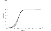
- FIG. 1 is a circuit diagram of a high frequency amplifier circuit according to a first embodiment of the present invention. It is a characteristic diagram showing a first relationship between the input gate bias voltage V GG and the drain current I DD in the high frequency amplifying circuit of the embodiment of the present invention. It is a characteristic diagram showing the relationship between the variation amount [Delta] V p and the drain current I DD of the pinch-off voltage V p in the high frequency amplifier circuit according to the first embodiment of the present invention.
- FIG. 6 is a characteristic diagram showing the relationship between the variation of the bias voltage V GG , the fluctuation amount ⁇ V p of the pinch-off voltage V p , and the drain current I DD in the high frequency amplifier circuit of the first embodiment of the present invention.
- FIG. 6 is a characteristic diagram showing a relationship between an input gate bias voltage V GG and a drain current I DD when a bias resistance is changed in the high frequency amplifier circuit of the present embodiment. It is a circuit diagram of the high frequency amplifier circuit which concerns on the 2nd Embodiment of this invention. It is a circuit diagram of the high frequency amplifier circuit which concerns on the 3rd Embodiment of this invention. It is a circuit diagram of the high frequency amplifier circuit which concerns on the 4th Embodiment of this invention.
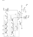
- FIG. 1 is a circuit diagram of a high-frequency amplifier circuit according to the first embodiment of the present invention.
- the high-frequency amplifier circuit 10 includes a field-effect transistor 101 (hereinafter simply referred to as “FET 101”) for high-frequency amplification.
- FET 101 is an enhancement type FET.
- the FET 101 is grounded at the source, and obtains power from the drain.
- the gate of the FET 101 is connected to the high frequency signal input terminal Pin through the input matching circuit 901.
- the gate of the FET 101 is connected to the gate bias voltage application terminal PVG via the gate bias voltage setting circuit 110.
- the drain of the FET 101 is connected to the drive voltage application terminal PVD via the choke coil 301 (inductance L1).
- a connection point between the choke coil 301 and the drive voltage application terminal PVD is connected to the ground via a bypass capacitor 401 (capacitance C1).
- connection point between the drain of the FET 101 and the choke coil 301 is connected to the high-frequency signal output terminal Pout via the output matching circuit 902.
- the input gate bias voltage V GG applied from the gate bias voltage application terminal P VG is stabilized by the gate bias voltage setting circuit 110 according to the characteristics of the FET 101, Compensated by the amplifying gate bias voltage V GG1 and applied to the gate of the FET 101.
- FET 101 is controlled to flow a drain current I DD to desired.
- the high frequency signal S RF is applied to the gate of the FET 101.
- RF signal S RF is amplified by the amplification factor corresponding to the drain current I DD by FET 101.
- the amplified high frequency signal S RF is output from the high frequency signal output terminal Pout via the output matching circuit 902.
- the gate bias voltage setting circuit 110 includes a constant voltage circuit 111 and a voltage compensation circuit 112.
- a resistor 201 and a constant voltage circuit 111 are connected in series between the gate bias voltage application terminal PVG and the ground.
- a connection point between the resistor 201 and the constant voltage circuit 111 is connected to the gate of the FET 101 via the voltage compensation circuit 112.
- the constant voltage circuit 111 includes three field effect transistors (FETs) 104, 105, and 106.
- the FETs 104, 105, and 106 are enhancement type FETs like the FET 101.
- the FETs 104, 105, and 106 and the FET 101 are manufactured on the same semiconductor substrate, and are further formed at close positions on the semiconductor substrate.
- FETs 104, 105, and 106 are connected in cascade between the resistor 201 and the ground. More specifically, the drain of the FET 104 is connected to the resistor 201, and the source of the FET 104 is connected to the drain of the FET 105. The source of the FET 105 is connected to the drain of the FET 106, and the source of the FET 106 is connected to the ground.
- the drain and gate of the FET 104 are connected.
- the drain and gate of the FET 105 are connected.
- the drain and gate of the FET 106 are connected.
- each FET 104, 105, 106 functions as a diode. Therefore, the three-stage cascade connection circuit of FETs 104, 105, and 106 is equivalent to a circuit in which three diodes are connected in series.
- the constant voltage circuit 110 including the three-stage cascade circuit of the FETs 104, 105, and 106 becomes a circuit that can obtain a constant voltage obtained by adding the pinch-off voltages of the FETs 104, 105, and 106.
- the voltage at the connection point between the resistor 201 and the constant voltage circuit 111 in other words, the input voltage of the voltage compensation circuit 112 (the voltage corresponding to V GG2 in FIG. 1) is the voltage by the constant voltage circuit. Become. As a result, even if the input gate bias voltage V GG varies, this variation can be suppressed to some extent, and a more stable voltage V GG2 can be obtained.
- the FETs 104, 105, and 106 are formed on the same semiconductor substrate to have the same characteristics as the FET 101, so that the pinch-off voltage of the FET 101 and the pinch-off voltages of the FETs 104, 105, and 106 are Therefore, the voltage V GG2 corresponding to the fluctuation rate of the pinch-off voltage of the FET 101 can be obtained.
- the voltage V GG2 is not always stable with high accuracy, and may vary due to variations in the input gate bias voltage V GG .
- the voltage compensation circuit 112 shown below suppresses the influence of such variations on the amplification gate bias voltage V GG1 of the FET 101.
- the voltage compensation circuit 112 includes FETs 102 and 103 and resistors 202, 203 and 204.
- the FETs 102 and 103 are composed of enhancement type FETs like the FETs 101, 104, 105, and 106.
- the FETs 102 and 103 and the FETs 101, 104, 105, and 106 are manufactured on the same semiconductor substrate, and are formed at positions adjacent to each other on the semiconductor substrate.
- the FETs 101 to 106 have the same gate voltage-drain current characteristics.
- the FET 102 corresponds to the first compensation field effect transistor of the present invention
- the FET 103 corresponds to the second compensation field effect transistor of the present invention.
- the gate of the FET 102 is connected to a connection point between the resistor 201 and the constant voltage circuit 111. Therefore, the gate bias voltage of the FET 102 is the voltage V GG2 described above.
- the drain of the FET 102 is connected to the drive voltage application terminal PVD via the choke coil 301.
- the source of the FET 102 is connected to the drain of the FET 103 through a series circuit of resistors 202 and 203.
- the FET 103 is grounded at the source.
- the gate of the FET 103 is connected to a connection point between the resistor 202 and the resistor 203.
- the drain of the FET 103 is connected to the gate of the FET 101 via the resistor 204.
- the voltage compensation circuit 112 having such a circuit configuration operates as follows.
- the drain current IDS2 in accordance with the voltage V GG2 flows.
- the drain current I DS2 flows through the resistors 202 and 203, and a voltage corresponding to the drain current I DS2 is generated in each of the resistors 202 and 203.
- the drain current I DS2 of the FET 102 increases.
- the current flowing through the resistors 202 and 203 increases, and the voltage across the resistors 202 and 203 increases.
- V GG2 decreases, the reverse operation is performed and the amplification gate bias voltage V GG1 does not change.
- the high frequency amplifier circuit of this embodiment is a characteristic diagram showing the relationship between the input gate bias voltage V GG and the drain current I DD when the there is no variation of the pinch-off voltage Vp.
- a predetermined value 1.8 [V] in this example
- the radio frequency amplifier circuit of the present embodiment is a characteristic diagram showing the relationship between the pinch-off voltage V p of the variation amount [Delta] V p and the drain current I DD when fixing the input gate bias voltage V GG. As shown in FIG. 3, even if the pinch-off voltage V p of the FET101 for high frequency amplification is changed, the drain current I DD is hardly changed.
- the drain current I DD having a desired current value is not affected by variations in the input gate bias voltage V GG and the pinch-off voltage V p of the FET 101 for high frequency amplification. Can be output stably.
- Figure 4 is a characteristic diagram showing the relationship between the bias voltage V GG variations and pinch-off voltage V p of the variation amount [Delta] V p and the drain current I DD of the radio frequency amplifier circuit of the present embodiment.
- Each characteristic curve in FIG. 4 has a different pinch-off voltage.
- drain by suppressing both the influence of the variation amount [Delta] V p of variation and the pinch-off voltage V p of the bias voltage V GG consists current value to the desired
- the current I DD can be output stably.
- the current for providing the amplification gate bias voltage V GG1 is the drain current I DS2 of the FET 102.
- the power supply for supplying the drain current IDS2 is the drive power supply voltage V DD applied from the drive voltage application terminal PVD .
- the drive power supply voltage V DD is a power supply for supplying a drain current, and can supply a larger amount of current than the input gate bias voltage VGG .
- the high frequency amplifier circuit 10 when used as a power amplifier, it may be operated up to the saturation region of the FET, and the gate current of the FET 101 for high frequency amplification increases particularly rapidly in the saturation region.
- a high-resistance series resistance is connected between the gate of the high-frequency amplification FET 101 and a terminal to which the gate bias voltage VGG is applied to the high-frequency amplification FET 101, a voltage is generated by the series resistance. A drop occurs, and the gate voltage of the FET 101 for high frequency amplification quickly becomes equal to or lower than the pinch-off voltage, and an increase in output power is suppressed.
- the resistance connected in series with the gate in order to increase the output power, the resistance connected in series with the gate must be lowered.
- the resistance when the resistance is lowered, the current flowing through the terminal to which the gate bias voltage VGG is applied increases. .
- the terminal to which the gate bias voltage VGG is applied is a control power source for the FET, there are many cases where the supply current is limited, and a large current cannot be handled. Therefore, in the conventional configuration, the resistance connected in series with the gate cannot be reduced.
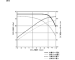
- FIG. 5 is a diagram showing the characteristics of the gate voltage and output power of the FET 101 for high frequency amplification in the high frequency amplifier circuit of the present invention and the conventional high frequency amplifier circuit when the high frequency input power is changed.
- the gate voltage of the FET 101 for high frequency amplification is less likely to be lower than that of the conventional configuration even if the power of the input high frequency signal is increased. That is, the effect that the value of the resistor connected in series with the gate is reduced is exhibited.
- higher output power than the conventional configuration can be obtained.
- FIG. 6 is a characteristic diagram showing the relationship between the input gate bias voltage V GG and the drain current I DD when the bias resistance is changed in the high frequency amplifier circuit of this embodiment.
- V GG input gate bias voltage
- I DD drain current I DD
- FIG. 7 is a circuit diagram of a high-frequency amplifier circuit according to the second embodiment of the present invention.
- the high-frequency amplifier circuit 10A of the present embodiment is different from the high-frequency amplifier circuit 10 according to the first embodiment in the configuration of the constant voltage circuit 111A, and other configurations are the same as those of the high-frequency amplifier circuit 10 according to the first embodiment. The same. Therefore, only different parts will be described below.
- the constant voltage circuit 111A is a circuit in which FETs 104A, 105A, and 106A are cascaded in three stages. Each FET 104A, 105A, 106A has a drain and a source connected. With this configuration, each of the FETs 104A, 105A and 106A can be made to function as a so-called Schottky diode because the drain and the source are short-circuited.
- the resistor 201 is connected to the input terminal (gate) of the FET 104A.
- the output terminal (drain, source) of the FET 104A is connected to the input terminal (gate) of the FET 105A.
- the output terminal (drain, source) of the FET 105A is connected to the input terminal (gate) of the FET 106A.
- the output terminal (drain, source) of the FET A is connected to the ground.
- FETs are cascade-connected, but the Schottky diode elements may be cascade-connected using a two-terminal Schottky diode element.
- FIG. 8 is a circuit diagram of a high-frequency amplifier circuit according to the third embodiment of the present invention.
- the high-frequency amplifier circuit 10B of the present embodiment is different from the high-frequency amplifier circuit 10 according to the first embodiment in the configuration of the constant voltage circuit 111B, and other configurations are the same as those of the high-frequency amplifier circuit 10 according to the first embodiment. The same. Therefore, only different parts will be described below.
- the constant voltage circuit 111B is a circuit in which n-type bipolar transistors 104B, 105B, and 106B are cascade-connected in three stages. Specifically, the resistor 201 is connected to the collector of the bipolar transistor 104B. The collector of the bipolar transistor 105B is connected to the emitter of the bipolar transistor 104B. The collector of the bipolar transistor 106B is connected to the emitter of the bipolar transistor 105B. The emitter of the bipolar transistor 106B is connected to the ground. The collector and base of the bipolar transistor 104B are directly connected to each other. The collector and base of the bipolar transistor 105B are directly connected to each other. The collector and base of the bipolar transistor 106B are directly connected to each other.
- FIG. 9 is a circuit diagram of a high-frequency amplifier circuit according to the fourth embodiment of the present invention.
- the high-frequency amplifier circuit 10C of this embodiment is such that a resistor 501 is connected between the drain of the FET 101 for high-frequency amplification and the drain of the FET 102 of the voltage compensation circuit 112, and the other configuration is the first embodiment. This is the same as the high-frequency amplifier circuit 10 according to FIG.
- This resistor 501 corresponds to the high impedance circuit of the present invention.
- FIG. 10 is a circuit diagram of a high-frequency amplifier circuit according to the fifth embodiment of the present invention.
- the high-frequency amplifier circuit 10D of this embodiment has a coil 601 connected between the drain of the FET 101 for high-frequency amplification and the drain of the FET 102 of the voltage compensation circuit 112, and the other configuration is the same as that of the first embodiment. This is the same as the high-frequency amplifier circuit 10.
- the resistor 501 shown in the fourth embodiment is replaced with the coil 601.
- This coil 601 corresponds to the high impedance circuit of the present invention.
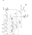
- FIG. 11 is a circuit diagram of a high-frequency amplifier circuit according to the sixth embodiment of the present invention.
- the high-frequency amplifier circuit 10E of this embodiment is configured by connecting a parallel resonant circuit of a coil 601 and a capacitor 602 between the drain of the FET 101 for high-frequency amplification and the drain of the FET 102 of the voltage compensation circuit 112. Is the same as the high-frequency amplifier circuit 10 according to the first embodiment.
- the resistor 501 shown in the fourth embodiment or the coil 601 shown in the fifth embodiment is replaced with a parallel resonance circuit of the coil 601 and the capacitor 602.
- the parallel resonant circuit of the coil 601 and the capacitor 602 corresponds to the high impedance circuit of the present invention.
- the element values of the coil 601 and the capacitor 602 are determined so that the resonance frequency of the parallel resonance circuit of the coil 601 and the capacitor 602 matches the frequency of the high-frequency signal amplified by the high-frequency amplifier circuit 10E.
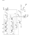
- FIG. 12 is a circuit diagram of a high-frequency amplifier circuit according to the seventh embodiment of the present invention.
- the high-frequency amplifier circuit 10F of the present embodiment is different from the high-frequency amplifier circuit 10 according to the first embodiment in the configuration of the constant voltage circuit 111F, and other configurations are the same as those of the high-frequency amplifier circuit 10 according to the first embodiment. The same. Therefore, only different parts will be described below.
- the constant voltage circuit 111F includes four field effect transistors (FETs) 104, 105, 106, and 107.
- the FETs 104, 105, 106, and 107 are enhancement type FETs.
- FETs 104, 105, 106, and 107 are connected in cascade between the resistor 201 and the ground. More specifically, the drain of the FET 104 is connected to the resistor 201, and the source of the FET 104 is connected to the drain of the FET 105. The source of the FET 105 is connected to the drain of the FET 106, the source of the FET 106 is connected to the drain of the FET 107, and the source of the FET 107 is connected to the ground.
- the drain and gate of the FET 104 are connected.
- the drain and gate of the FET 105 are connected.
- the drain and gate of the FET 106 are connected.
- the drain and gate of the FET 107 are connected.
- a constant voltage circuit composed of cascaded four-stage FETs can be realized.
- the number of cascade-connected FETs for configuring the constant voltage circuit is not limited to three as shown in the first embodiment, and the number of stages may be set as appropriate according to use. . This is the same even when a bipolar transistor is used.
Landscapes
- Engineering & Computer Science (AREA)
- Power Engineering (AREA)
- Amplifiers (AREA)
Abstract
高周波増幅回路(10)は、高周波増幅用のFET(101)、定電圧回路(111)、電圧補償回路(112)を備える。ゲートバイアス電圧印加端子(PVG)とグランドとの間には、抵抗器(201)と定電圧回路(111)が直列接続されている。抵抗器(201)と定電圧回路(111)との接続点とFET(101)との間には、電圧補償回路(112)が接続されている。電圧補償回路(110)は、抵抗器(201)と定電圧回路(111)との接続点にゲートが接続するFET(102)と、FET(102)のソースとグランドとの間に直列接続された抵抗器(202,203)、FET(103)を備える。FET(103)のゲートは抵抗器(202,203)の接続点に接続し、FET(103)のドレインは、抵抗器(204)を介してFET(101)のゲートに接続している。
Description
本発明は、入力された高周波信号を増幅して出力する高周波増幅回路、特に、エンハンスメント型の電界効果トランジスタを増幅素子として用いる高周波増幅回路に関する。
従来、通信機器の送信回路には、通信に利用する高周波信号を増幅する高周波増幅回路が備えられている。基本的な高周波増幅回路の構成としては、例えば、特許文献1の従来技術の図6にも示されているように、高周波信号増幅用の電界効果トランジスタ(以下、「FET」と称する。)が備えられており、抵抗器を介して高周波増幅用FETのゲートバイアス電圧が印加されている。
この構成では、高周波増幅用FETの製造バラツキによりドレイン電流がばらつくことが分かっており、特許文献1に記載の高周波増幅回路では、次の構成を備えている。
高周波増幅用FETのゲートには、高周波増幅用FETと同じ構造からなる補償用FETを含むゲートバイアス回路が備えられている。ゲートバイアス回路は、ゲートバイアス(-VGG)の印加端子とグランドとの間に、補償用FETと二個の抵抗器とが縦続接続された構成からなる。具体的には、ゲートバイアス(-VGG)の印加端子側から、抵抗器、補償用FET、抵抗器が接続される。各抵抗器は、補償用FETのドレインとソースに接続される。補償用FETのゲートには、ゲートバイアス(-VGG)が直接印加される。
このような構成の場合、高周波増幅用FETのピンチオフ電圧が設計値からずれた場合、補償用FETのピンチオフ電圧も同じように設計値からずれる。この補償用FETのピンチオフ電圧のズレによって、ゲートバイアス回路の出力電圧(高周波増幅用FETのゲートバイアス電圧)が、ピンチオフ電圧のズレを補償するように変化する。
このような構成からなる特許文献1に記載の高周波増幅用FETと補償用FETは、デプレッション側のFETからなる。
また、従来の高周波増幅回路として、図13に示す高周波増幅回路がある。図13は、従来の高周波増幅回路の回路図である。高周波増幅回路10Pは、高周波増幅用の電界効果トランジスタ101(FET101)を備える。FET101は、エンハンスメント型からなる。FET101のゲートは、入力整合回路901を介して、高周波信号入力端子Pinが接続されている。
また、FET101のゲートは、ゲートバイアス電圧設定回路110Pを介して、ゲートバイアス電圧印加端子PVGに接続されている。ゲートバイアス電圧設定回路110Pは、ゲートバイアス電圧印加端子PVGとグランドとの間に直列接続された抵抗器211P,212Pを備える。抵抗器211P,212Pの接続点は、抵抗器213Pを介して、FET101のゲートに接続されている。
このような構成では、抵抗器211P,212Pの抵抗比を変化させることで、FET101のゲートバイアス電圧を変化させ、FET101のドレイン電流すなわち高周波増幅回路10Pの出力電力を調整している。
しかしながら、特許文献1に記載の高周波増幅回路は、各FETにデプレッション型FETを用いている。したがって、特許文献1には、高周波増幅回路における高周波増幅用FETの製造バラツキによるドレイン電流のばらつきを抑制する方法について、エンハンスメント型FETを用いた場合に関しての記載が無い。
また、特許文献1に記載の高周波増幅回路では、図13に示した従来の高周波増幅回路10Pと同様に、入力するゲートバイアス電圧を変化させなければ、ドレイン電流を制御することができない。
また、図13に示した従来の高周波増幅回路10Pでは、次に示す問題が生じる。図14は従来の高周波増幅回路のゲートバイアス電圧とドレイン電流との関係を示す特性図である。図15は従来の高周波増幅回路においてゲートバイアス電圧を固定した時のピンチオフ電圧の変動分とドレイン電流との関係を示す特性図である。
図14に示すように、従来の高周波増幅回路10Pでは、ゲートバイアス電圧VGGとドレイン電流IDDとの関係は非線形であり、ゲートバイアス電圧VGGが所定値以上になると、急激にドレイン電流IDDが増加する。
高周波増幅回路として高い出力電力を得ようとする場合、このドレイン電流IDDが非線形で急激に変化する領域のゲートバイアス電圧VGGを用いなければならない。しかしながら、この領域を用いた場合、ゲートバイアス電圧VGGの変化に応じたドレイン電流IDDの変化量が大きく、目標とした出力電力を安定して得ることが難しい。
また、図15に示すように、高周波増幅用のFETのピンチオフ電圧の変動量に応じたドレイン電流IDDの変化量も非線形である。特に、所定のピンチオフ電圧が低くなった場合には、同じベースバイアス電圧であっても、ピンチオフ電圧が高い時と比較して、急激にドレイン電流IDDが増加する。
このように、ゲートバイアス電圧VGGが安定であっても、高周波増幅用のFET101のピンチオフ電圧にバラツキが生じると、同様にドレイン電流が大幅に変化してしまう。
本発明の目的は、ゲートバイアス電圧VGGや高周波増幅用FETのピンチオフオフ電圧にバラツキがあっても、安定した出力電力を得られる高周波増幅回路を提供することにある。
この発明は、高周波増幅用の電界効果トランジスタと、該電界効果トランジスタのゲートバイアスを決定するゲートバイアス電圧設定回路と、を備えた高周波増幅回路に関するものであり、次の特徴を有する。高周波増幅用の電界効果トランジスタはエンハンスメント型である。ゲートバイアス電圧設定回路は、外部入力される入力ゲートバイアス電圧VGGが印加された状態で所定電圧を出力する定電圧回路と、エンハンスメント型の複数の補償用電界効果トランジスタを有する電圧補償回路とを備える。複数の補償用電界効果トランジスタは、定電圧回路から入力される電圧が印加される第1の補償用電界効果トランジスタと、該第1の補償用電界効果トランジスタのドレイン電流の増加によりドレインソース間のオン抵抗が低下し、第1の補償用の電界効果トランジスタのドレイン電流の低下によりドレインソース間のオン抵抗が上昇する第2の補償用電界効果トランジスタを、有する。
この構成では、ゲートバイアス電圧設定回路に入力される電圧が変動した場合に、ゲートバイアス電圧設定回路から出力される電圧、すなわち高周波増幅用の電界効果トランジスタのゲートバイアス電圧が調整され、高周波増幅用の電界効果トランジスタのドレイン電流は一定に保たれる。同様に、高周波増幅用の電界効果トランジスタのピンチオフ電圧が設計値からずれている場合であっても、高周波増幅用の電界効果トランジスタのゲートバイアス電圧が調整され、高周波増幅用の電界効果トランジスタのドレイン電流は一定に保たれる。
また、この発明の高周波増幅回路は、次の構成であってもよい。第2の補償用電界効果トランジスタはソース接地されている。第1の補償用電界効果トランジスタのソースと第2の補償用電界効果トランジスタのドレインとの間には、二個の抵抗器が直列接続されている。第2の補償用電界効果トランジスタのゲートは、二個の抵抗器の接続点に接続されている。第2の補償用電界効果トランジスタのドレインは、高周波増幅用の電界効果トランジスタのゲートに接続されている。
この構成では、電圧補償回路の具体的な回路構成例を示している。
また、この発明の高周波増幅回路では、第1の補償用電界効果トランジスタのドレインは、高周波増幅用の電界効果トランジスタのドレインと同じ駆動電圧印加端子に接続されていることが好ましい。
この構成では、高周波増幅用の電界効果トランジスタのゲートに印加可能な電流を大きくすることができる。これにより、高周波増幅用の電界効果トランジスタのゲートに直列接続する抵抗器を低抵抗にしても、ゲートに大きな電流を供給できる。したがって、高周波増幅回路の出力特性を向上させることができる。
また、この発明の高周波増幅回路では、第1の補償用電界効果トランジスタのドレインと、高周波増幅用の電界効果トランジスタのドレインとの間に、高周波信号に対して高インピーダンスとなる高インピーダンス回路が接続されていることが好ましい。
この構成では、高周波増幅用の電界効果トランジスタから出力される増幅後の高周波信号が、高周波増幅用の電界効果トランジスタのゲート電圧を供給する回路側に帰還することを抑制できる。これにより、高周波増幅回路の出力特性をさらに向上させることができる。
また、この発明の高周波増幅回路の高インピーダンス回路は抵抗器であってもよい。
また、この発明の高周波増幅回路の高インピーダンス回路はコイルであってもよい。
また、この発明の高周波増幅回路の高インピーダンス回路は、高周波信号の周波数を共振周波数とするコイルとコンデンサの並列共振回路であってもよい。
これらの構成では、高インピーダンス回路の具体的な回路構成例を示している。
また、この発明の高周波増幅回路の定電圧回路は、エンハンスメント型の複数の定電圧用電界効果トランジスタを備え、複数の定電圧用電界効果トランジスタは、それぞれがダイオード接続され、且つ、縦続接続されていることが好ましい。
この構成では、定電圧回路の具体的な構成例を示している。このように、高周波増幅用の電界効果トランジスタと同じ特性の電界効果トランジスタのみで定電圧回路を構成することで、高周波増幅用の電界効果トランジスタのピンチオフ電圧と同じような変動特性で定電圧回路の電圧も変化する。したがって、高周波増幅用の電界効果トランジスタのピンチオフ電圧に応じた適切で安定な電圧を発生することができる。
また、この発明の高周波増幅回路の定電圧回路は、複数のn型のバイポーラトランジスタを備え、複数のn型のバイポーラトランジスタは、それぞれがダイオード接続され、且つ、縦続接続されていてもよい。
この構成では、定電圧回路をバイポーラトランジスタで構成する場合を示している。このようなバイポーラトランジスタであっても、定電圧回路を構成することができ、安定した電圧を出力することができる。
この発明によれば、ゲートバイアス電圧VGGや高周波増幅用のFETのピンチオフオフ電圧にバラツキがあっても、高周波増幅用のFETのドレイン電流を安定させることができる。これにより、安定した出力電力の高周波増幅回路を実現することができる。
本発明の第1の実施形態に係る高周波増幅回路について、図を参照して説明する。図1は、本発明の第1の実施形態に係る高周波増幅回路の回路図である。
高周波増幅回路10は、高周波増幅用の電界効果トランジスタ101(以下、単に「FET101」と称する。)を備える。FET101は、エンハンスメント型のFETである。FET101はソース接地されており、ドレインから電力を得る。
FET101のゲートは、入力整合回路901を介して、高周波信号入力端子Pinに接続されている。FET101のゲートは、ゲートバイアス電圧設定回路110を介して、ゲートバイアス電圧印加端子PVGに接続されている。
FET101のドレインは、チョークコイル301(インダクタンスL1)を介して、駆動電圧印加端子PVDに接続されている。チョークコイル301と駆動電圧印加端子PVDとの接続点は、バイパスコンデンサ401(キャパシタンスC1)を介して、グランドに接続されている。
FET101のドレインとチョークコイル301の接続点は、出力整合回路902を介して、高周波信号出力端子Poutに接続されている。
このような回路構成からなる高周波信号増幅回路10は、ゲートバイアス電圧印加端子PVGから印加された入力ゲートバイアス電圧VGGがゲートバイアス電圧設定回路110で、FET101の特性に応じて安定化され、増幅用ゲートバイアス電圧VGG1に補償されてFET101のゲートに印加される。これにより、FET101は、所望とするドレイン電流IDDが流れるように制御される。
このようなFET101に対して、高周波信号入力端子Pinから高周波信号SRFを印加すると、高周波信号SRFは、入力整合回路901を介して、FET101のゲートに印加される。
高周波信号SRFは、FET101によってドレイン電流IDDに応じた増幅率で増幅される。増幅された高周波信号SRFは、出力整合回路902を介して高周波信号出力端子Poutから出力される。
次に、ゲートバイアス電圧設定回路110の具体的な構成について説明する。ゲートバイアス電圧設定回路110は、定電圧回路111、電圧補償回路112を備える。ゲートバイアス電圧印加端子PVGとグランドとの間には、抵抗器201と定電圧回路111とが直列接続されている。抵抗器201と定電圧回路111との接続点は、電圧補償回路112を介して、FET101のゲートに接続されている。
定電圧回路111は、三個の電界効果トランジスタ(FET)104,105,106からなる。FET104,105,106は、FET101と同じくエンハンスメント型のFETで構成されている。例えば、FET104,105,106とFET101は、同じ半導体基板上に製造されたものであり、さらには、当該半導体基板上の近接する位置に形成されている。
FET104,105,106は、抵抗器201とグランドとの間に、縦続接続されている。より具体的には、FET104のドレインは抵抗器201に接続されており、FET104のソースはFET105のドレインに接続されている。FET105のソースはFET106のドレインに接続されており、FET106のソースはグランドに接続されている。
FET104のドレインとゲートは接続されている。FET105のドレインとゲートは接続されている。FET106のドレインとゲートは接続されている。この構成により、それぞれのFET104,105,106はダイオードとして機能する。したがって、FET104,105,106の三段縦続接続回路は、ダイオードが三個直列接続された回路と等価になる。
これにより、FET104,105,106の三段縦続接続回路からなる定電圧回路110は、FET104,105,106のピンチオフ電圧を加算した定電圧が得られる回路となる。
このような回路構成から、抵抗器201と定電圧回路111との接続点の電圧、言い換えれば電圧補償回路112の入力電圧(図1のVGG2に相当する電圧)は、定電圧回路による電圧となる。これにより、入力ゲートバイアス電圧VGGにバラツキがあっても、このバラツキをある程度抑制して、より安定した電圧VGG2を得ることができる。特に、本実施形態に示すように、FET104,105,106を同じ半導体基板上に形成するなどFET101と同じ特性のものとすることで、FET101のピンチオフ電圧と、FET104,105,106のピンチオフ電圧とが同じ変動率となるので、FET101のピンチオフ電圧の変動率に応じた電圧VGG2を得ることができる。
ただし、この電圧VGG2も高精度に安定であるとは限らず、入力ゲートバイアス電圧VGGのバラツキにより、バラツキを有することがある。このようなバラツキが、FET101の増幅用ゲートバイアス電圧VGG1に与える影響を、次に示す電圧補償回路112によって抑制している。
電圧補償回路112は、FET102,103、抵抗器202,203,204を備える。
FET102,103は、FET101,104,105,106と同じくエンハンスメント型のFETで構成されている。例えば、FET102,103とFET101,104,105,106は、同じ半導体基板上に製造されたものであり、さらには、当該半導体基板上の近接する位置に形成されている。このように、全てのFET101~106を同じエンハンスメント型にすることのより、FET101~106は、ゲート電圧-ドレイン電流特性が同じになる。FET102は本発明の第1の補償用電界効果トランジスタに相当し、FET103は本発明の第2の補償用電界効果トランジスタに相当する。
FET102のゲートは、抵抗器201と定電圧回路111との接続点に接続されている。したがって、FET102のゲートバイアス電圧は、上述の電圧VGG2となる。FET102のドレインは、チョークコイル301を介して駆動電圧印加端子PVDに接続されている。
FET102のソースは、抵抗器202,203の直列回路を介して、FET103のドレインに接続されている。FET103はソース接地されている。FET103のゲートは、抵抗器202と抵抗器203との接続点に接続されている。FET103のドレインは、抵抗器204を介してFET101のゲートに接続されている。
このような回路構成からなる電圧補償回路112は、次に示すように動作する。FET102に電圧VGG2が印加されると、当該電圧VGG2に応じたドレイン電流IDS2が流れる。ドレイン電流IDS2は抵抗器202,203に流れ、抵抗器202と抵抗器203とでそれぞれにドレイン電流IDS2に応じた電圧が発生する。
抵抗器202と抵抗器203との接続点は、FET103のゲートに接続されているので、ドレイン電流IDSD2が流れると、抵抗器202と抵抗器203とによる分圧比に応じた電圧VGG3がFET103のゲートに印加される。FET103に電圧VGG3が印加されると、FET103のオン抵抗に応じたドレインソース間電圧が生じる。これが電圧補償回路の出力電圧に相当する電圧VGG4となる。この電圧VGG4は、抵抗器204を介してFET101のゲートに印加され、FET101のゲートには増幅用ゲートバイアス電圧VGG1が印加される。
このような構成では、FET102のゲート電圧VGG2が変動した場合に、各電圧は次に示すように変化する。
例えば、VGG2が上昇した場合、FET102のドレイン電流IDS2は増加する。ドレイン電流IDS2が増加すると、抵抗器202,203に流れる電流が増加し、抵抗器202,203の両端電圧が増加する。
抵抗器203の両端電圧が増加すると、FET103のゲート電圧VGG3が上昇し、FET103のオン抵抗が低下する。FET103のドレインソース間電圧が上昇することが抑制される。この際、FET102,103が同じ特性を有するので、電圧VGG2による電圧変動は結果的に打ち消され、電圧VGG4は上昇しない。したがって、増幅用ゲートバイアス電圧VGG1も変化しない。
なお、VGG2が低下した場合は、この逆の動作となり、増幅用ゲートバイアス電圧VGG1は変化しない。
このように本実施形態の構成を用いることで、入力ゲートバイアス電圧VGGのバラツキがあっても、高周波増幅用のFET101のドレイン電流IDDを、所望の値で安定して出力することができる。
また、ピンチオフ電圧が異なるロットの高周波増幅回路の場合であっても、FET101~106が同じ特性を有するので、入力ゲートバイアス電圧VGGが変動する場合と同様に、高周波増幅用のFET101のドレイン電流IDDの変動を抑制する作用効果を得ることができる。
次に、本実施形態の構成を用いたことによる効果を、図2から図6を用いて説明する。
図2は、本実施形態の高周波増幅回路において、ピンチオフ電圧Vpの変動がないとした時の入力ゲートバイアス電圧VGGとドレイン電流IDDとの関係を示す特性図である。図2に示すように、入力ゲートバイアス電圧VGGが所定値(本例では1.8[V])以上であれば、入力ゲートバイアス電圧VGGが変化しても、ドレイン電流IDDは殆ど変化しない。
図3は、本実施形態の高周波増幅回路において、入力ゲートバイアス電圧VGGを固定した時のピンチオフ電圧Vpの変動量ΔVpとドレイン電流IDDとの関係を示す特性図である。図3に示すように、高周波増幅用のFET101のピンチオフ電圧Vpが変化しても、ドレイン電流IDDは殆ど変化しない。
このように本実施形態の構成を用いることで、入力ゲートバイアス電圧VGGや高周波増幅用のFET101のピンチオフ電圧Vpのバラツキに影響されることなく、所望とする電流値からなるドレイン電流IDDを安定して出力することができる。
図4は、本実施形態の高周波増幅回路におけるバイアス電圧VGGのバラツキとピンチオフ電圧Vpの変動量ΔVpとドレイン電流IDDとの関係を示す特性図である。図4における各特性曲線は、それぞれピンチオフ電圧が異なる。図4に示すように、本実施形態の構成を用いることで、バイアス電圧VGGのバラツキとピンチオフ電圧Vpの変動量ΔVpの双方の影響を抑圧して、所望とする電流値からなるドレイン電流IDDを安定して出力することができる。
さらに、本実施形態の構成では、次に示すような効果が得られる。
本実施形態の構成では、図1に示すように、増幅用ゲートバイアス電圧VGG1を与えるための電流が、FET102のドレイン電流IDS2である。そして、当該ドレイン電流IDS2を供給するための電源は、駆動電圧印加端子PVDから印加される駆動電源電圧VDDである。一般に、駆動電源電圧VDDは、ドレイン電流を供給するための電源であり、入力ゲートバイアス電圧VGGよりも電流供給量を多くすることができる。
ここで、高周波増幅回路10をパワーアンプとして利用する場合、FETの飽和領域まで動作させることがあり、飽和領域では特に高周波増幅用のFET101のゲート電流が急激に増加する。この際、高周波増幅用のFET101のゲートと、当該高周波増幅用のFET101にゲートバイアス電圧VGGを印加する端子との間に、高抵抗の直列抵抗が接続されていると、当該直列抵抗により電圧降下が生じて、高周波増幅用のFET101のゲート電圧がより早くピンチオフ電圧以下になってしまい、出力電力の増加が抑制される。ここで、出力電力を増加させるためには、ゲートに直列接続される抵抗を低くしなければならないが、抵抗を低くした場合、ゲートバイアス電圧VGGを印加する端子に流れる電流が増加してしまう。しかし、ゲートバイアス電圧VGGを印加する端子は、FETの制御電源であるので、供給電流に制限がある場合が多く、大電流に対応できない。したがって、従来の構成では、ゲートに直列接続される抵抗を低くすることができなかった。
しかしながら、本実施形態の構成では、FET102を介して、高周波増幅用のFET101のゲートに対して電流を多く供給できることで、ゲートに直列接続される抵抗(抵抗器202,203,204に相当)を低抵抗化することができる。これにより、高周波増幅回路の出力電力を向上させることができる。
図5は、高周波入力電力を変化させた場合における本発明の高周波増幅回路と従来の高周波増幅回路における高周波増幅用のFET101のゲート電圧と出力電力との特性を示す図である。図5に示すように、本実施形態の構成を用いることで、入力される高周波信号の電力を増加させても、高周波増幅用のFET101のゲート電圧は、従来構成よりも低下しにくい。すなわち、ゲートに直列に接続される抵抗の値が小さくなっている効果が発揮されていることになる。さらに、本実施形態の構成を用いることで、従来構成よりも高い出力電力を得ることができる。
また、次に示す効果を得ることもできる。図6は、本実施形態の高周波増幅回路におけるバイアス抵抗を変化させた場合の入力ゲートバイアス電圧VGGとドレイン電流IDDとの関係を示す特性図である。図6に示すように、バイアス抵抗(抵抗器202,203)を変化させることにより、ドレイン電流IDDの電流値を変化させることができる。この際、いずれのバイアス抵抗値を採用しても、VGGの変動による影響を抑制することができるので、高周波増幅回路におけるドレイン電流IDDの調整が容易になる。
次に、本発明の第2の実施形態に係る高周波増幅回路について、図を参照して説明する。図7は、本発明の第2の実施形態に係る高周波増幅回路の回路図である。本実施形態の高周波増幅回路10Aは、定電圧回路111Aの構成が第1の実施形態に係る高周波増幅回路10と異なるものであり、他の構成は第1の実施形態に係る高周波増幅回路10と同じである。したがって、異なる箇所のみを以下に説明する。
定電圧回路111Aは、FET104A,105A,106Aが三段縦続接続された回路である。各FET104A,105A,106Aはドレインとソースが接続されている。この構成により、各FET104A,105A,106Aはドレインとソースが短絡されるので、所謂ショットキーダイオードとして機能させることができる。抵抗器201には、FET104Aの入力端(ゲート)が接続されている。FET104Aの出力端(ドレイン、ソース)はFET105Aの入力端(ゲート)に接続されている。FET105Aの出力端(ドレイン、ソース)はFET106Aの入力端(ゲート)に接続されている。FETAの出力端(ドレイン、ソース)はグランドに接続されている。なお、本実施形態では、FETを縦続接続する例を示したが、二端子のショットキーダイオード素子を用いて、当該ショットキーダイオード素子を縦続接続してもよい。
このような構成であっても、第1の実施形態と同様に定電圧回路として機能し、第1の実施形態に係る高周波増幅回路10と同じ作用効果を得ることができる。
次に、本発明の第3の実施形態に係る高周波増幅回路について、図を参照して説明する。図8は、本発明の第3の実施形態に係る高周波増幅回路の回路図である。本実施形態の高周波増幅回路10Bは、定電圧回路111Bの構成が第1の実施形態に係る高周波増幅回路10と異なるものであり、他の構成は第1の実施形態に係る高周波増幅回路10と同じである。したがって、異なる箇所のみを以下に説明する。
定電圧回路111Bは、n型のバイポーラトランジスタ104B,105B,106Bが三段縦続接続された回路である。具体的には、抵抗器201には、バイポーラトランジスタ104Bのコレクタが接続されている。バイポーラトランジスタ104Bのエミッタはバイポーラトランジスタ105Bのコレクタが接続されている。バイポーラトランジスタ105Bのエミッタはバイポーラトランジスタ106Bのコレクタが接続されている。バイポーラトランジスタ106Bのエミッタはグランドに接続されている。バイポーラトランジスタ104Bのコレクタとベースは互いに直接接続されている。バイポーラトランジスタ105Bのコレクタとベースは互いに直接接続されている。バイポーラトランジスタ106Bのコレクタとベースは互いに直接接続されている。
このような構成であっても、第1の実施形態と同様に定電圧回路として機能し、第1の実施形態に係る高周波増幅回路10と同じ作用効果を得ることができる。
次に、本発明の第4の実施形態に係る高周波増幅回路について、図を参照して説明する。図9は、本発明の第4の実施形態に係る高周波増幅回路の回路図である。本実施形態の高周波増幅回路10Cは、高周波増幅用のFET101のドレインと電圧補償回路112のFET102のドレインとの間に抵抗器501が接続されたものであり、他の構成は第1の実施形態に係る高周波増幅回路10と同じである。この抵抗器501が本発明の高インピーダンス回路に相当する。
このような構成とすることで、高周波増幅用のFET101から出力される高周波信号が、抵抗器501で減衰されて、電圧補償回路112のFET102のドレインに帰還することを抑制できる。これにより、増幅用ゲートバイアス電圧VGG1を、より安定化することができる。
次に、本発明の第5の実施形態に係る高周波増幅回路について、図を参照して説明する。図10は、本発明の第5の実施形態に係る高周波増幅回路の回路図である。本実施形態の高周波増幅回路10Dは、高周波増幅用のFET101のドレインと電圧補償回路112のFET102のドレインとの間にコイル601が接続されたものであり、他の構成は第1の実施形態に係る高周波増幅回路10と同じである。言い換えれば、第4の実施形態に示した抵抗器501がコイル601に置き換わったものである。このコイル601が本発明の高インピーダンス回路に相当する。
このような構成とすることで、高周波増幅用のFET101から出力される高周波信号が、コイル601で減衰されて、電圧補償回路112のFET102のドレインに帰還することを抑制できる。これにより、増幅用ゲートバイアス電圧VGG1を、より安定化することができる。
次に、本発明の第6の実施形態に係る高周波増幅回路について、図を参照して説明する。図11は、本発明の第6の実施形態に係る高周波増幅回路の回路図である。本実施形態の高周波増幅回路10Eは、高周波増幅用のFET101のドレインと電圧補償回路112のFET102のドレインとの間にコイル601とコンデンサ602の並列共振回路が接続されたものであり、他の構成は第1の実施形態に係る高周波増幅回路10と同じである。言い換えれば、第4の実施形態に示した抵抗器501または第5の実施形態に示したコイル601がコイル601とコンデンサ602の並列共振回路に置き換わったものである。このコイル601とコンデンサ602との並列共振回路が本発明の高インピーダンス回路に相当する。
この際、コイル601とコンデンサ602との並列共振回路の共振周波数が、当該高周波増幅回路10Eで増幅する高周波信号の周波数に一致するように、コイル601とコンデンサ602の素子値を決定する。
このような構成とすることで、高周波増幅用のFET101から出力される高周波信号が、コイル601とコンデンサ602の並列共振回路で減衰されて、電圧補償回路112のFET102のドレインに帰還することを抑制できる。これにより、増幅用ゲートバイアス電圧VGG1を、より安定化することができる。
次に、本発明の第7の実施形態に係る高周波増幅回路について、図を参照して説明する。図12は、本発明の第7の実施形態に係る高周波増幅回路の回路図である。本実施形態の高周波増幅回路10Fは、定電圧回路111Fの構成が第1の実施形態に係る高周波増幅回路10と異なるものであり、他の構成は第1の実施形態に係る高周波増幅回路10と同じである。したがって、異なる箇所のみを以下に説明する。
定電圧回路111Fは、四個の電界効果トランジスタ(FET)104,105,106,107からなる。FET104,105,106,107は、エンハンスメント型のFETである。
FET104,105,106,107は、抵抗器201とグランドとの間に、縦続接続されている。より具体的には、FET104のドレインは抵抗器201に接続されており、FET104のソースはFET105のドレインに接続されている。FET105のソースはFET106のドレインに接続されており、FET106のソースはFET107のドレインに接続されており、FET107のソースはグランドに接続されている。
FET104のドレインとゲートは接続されている。FET105のドレインとゲートは接続されている。FET106のドレインとゲートは接続されている。FET107のドレインとゲートは接続されている。
このような構成により、四段のFETの縦続接続からなる定電圧回路を実現できる。このように、定電圧回路を構成するために縦続接続するFET数は、第1の実施形態に示すように三段であることに限るものではなく、使用に応じて段数は適宜設定すればよい。これは、バイポーラトランジスタを用いる場合でも同じである。
なお、上述の各実施形態を組み合わせた回路構成であっても、第1の実施形態に係る高周波増幅回路10と同じ作用効果を得ることができる。
10,10A,10B,10C,10D,10E,10F,10P:高周波増幅回路、
101:高周波増幅用のFET、
102,103,104,105,106,104A,105A,106A:FET、
104B,105B,106B:バイポーラトランジスタ、
201,202,203,204,211P,212P,213P,501:抵抗器、
301:チョークコイル、
401:バイパスコンデンサ、
601:コイル、
602:コンデンサ、
110,110P:ゲートバイアス電圧設定回路、
111,111A,111B:定電圧回路、
112:電圧補償回路、
901:入力整合回路、
902:出力整合回路、
Pin:高周波信号入力端子、
Pout:高周波信号出力端子、
PVG:ゲートバイアス電圧印加端子、
PVD:駆動電圧印加端子
101:高周波増幅用のFET、
102,103,104,105,106,104A,105A,106A:FET、
104B,105B,106B:バイポーラトランジスタ、
201,202,203,204,211P,212P,213P,501:抵抗器、
301:チョークコイル、
401:バイパスコンデンサ、
601:コイル、
602:コンデンサ、
110,110P:ゲートバイアス電圧設定回路、
111,111A,111B:定電圧回路、
112:電圧補償回路、
901:入力整合回路、
902:出力整合回路、
Pin:高周波信号入力端子、
Pout:高周波信号出力端子、
PVG:ゲートバイアス電圧印加端子、
PVD:駆動電圧印加端子
Claims (9)
- 高周波増幅用の電界効果トランジスタと、該電界効果トランジスタのゲートバイアスを決定するゲートバイアス電圧設定回路と、を備えた高周波増幅回路であって、
前記高周波増幅用の電界効果トランジスタはエンハンスメント型であり、
前記ゲートバイアス電圧設定回路は、
外部入力される入力ゲートバイアス電圧VGGが印加された状態で、所定電圧を出力する定電圧回路と、
エンハンスメント型の複数の補償用電界効果トランジスタを有する電圧補償回路とを備え、
該複数の補償用電界効果トランジスタは、
前記定電圧回路から入力される電圧が印加される第1の補償用電界効果トランジスタと、
該第1の補償用電界効果トランジスタのドレイン電流の増加によりドレインソース間のオン抵抗が低下し、前記第1の補償用の電界効果トランジスタのドレイン電流の低下によりドレインソース間のオン抵抗が上昇する第2の補償用電界効果トランジスタを、有する、高周波増幅回路。 - 前記第2の補償用電界効果トランジスタはソース接地されており、
前記第1の補償用電界効果トランジスタのソースと前記第2の補償用電界効果トランジスタのドレインとの間には、二個の抵抗器が直列接続されており、
前記第2の補償用電界効果トランジスタのゲートは、前記二個の抵抗器の接続点に接続されており、
前記第2の補償用電界効果トランジスタのドレインが、前記高周波増幅用の電界効果トランジスタのゲートに接続されている、
請求項1に記載の高周波増幅回路。 - 前記第1の補償用電界効果トランジスタのドレインは、前記高周波増幅用の電界効果トランジスタのドレインと同じ駆動電圧印加端子に接続されている、
請求項2に記載の高周波増幅回路。 - 前記前記第1の補償用電界効果トランジスタのドレインと、前記高周波増幅用の電界効果トランジスタのドレインとの間に、前記高周波信号に対して高インピーダンスとなる高インピーダンス回路が接続されている、
請求項3に記載の高周波増幅回路。 - 前記高インピーダンス回路は抵抗器である、請求項4に記載の高周波増幅回路。
- 前記高インピーダンス回路はコイルである、請求項4に記載の高周波増幅回路。
- 前記高インピーダンス回路は、前記高周波信号の周波数を共振周波数とするコイルとコンデンサの並列共振回路である、請求項4に記載の高周波増幅回路。
- 前記定電圧回路は、エンハンスメント型の複数の定電圧用電界効果トランジスタを備え、
前記複数の定電圧用電界効果トランジスタは、それぞれがダイオード接続され、且つ、縦続接続されている、請求項1乃至請求項7のいずれかに記載の高周波増幅回路。 - 前記定電圧回路は、複数のn型のバイポーラトランジスタを備え、
前記複数のn型のバイポーラトランジスタは、それぞれがダイオード接続され、且つ、縦続接続されている、請求項1乃至請求項7のいずれかに記載の高周波増幅回路。
Applications Claiming Priority (2)
| Application Number | Priority Date | Filing Date | Title |
|---|---|---|---|
| JP2012-254840 | 2012-11-21 | ||
| JP2012254840 | 2012-11-21 |
Publications (1)
| Publication Number | Publication Date |
|---|---|
| WO2014080668A1 true WO2014080668A1 (ja) | 2014-05-30 |
Family
ID=50775860
Family Applications (1)
| Application Number | Title | Priority Date | Filing Date |
|---|---|---|---|
| PCT/JP2013/070842 Ceased WO2014080668A1 (ja) | 2012-11-21 | 2013-08-01 | 高周波増幅回路 |
Country Status (1)
| Country | Link |
|---|---|
| WO (1) | WO2014080668A1 (ja) |
Cited By (2)
| Publication number | Priority date | Publication date | Assignee | Title |
|---|---|---|---|---|
| FR3059492A1 (fr) * | 2016-11-29 | 2018-06-01 | Stmicroelectronics (Grenoble 2) Sas | Procede et dispositif d'amplification en mode commun autopolarise et autoregule. |
| WO2021186694A1 (ja) * | 2020-03-19 | 2021-09-23 | 三菱電機株式会社 | 半導体装置 |
Citations (5)
| Publication number | Priority date | Publication date | Assignee | Title |
|---|---|---|---|---|
| JPS5552611A (en) * | 1978-10-11 | 1980-04-17 | Nec Corp | Constant-current circuit |
| JPH0284761A (ja) * | 1988-09-21 | 1990-03-26 | Nec Corp | 基準電圧発生回路 |
| JP2006339837A (ja) * | 2005-05-31 | 2006-12-14 | Alps Electric Co Ltd | 集積回路化高周波増幅器 |
| JP2007037149A (ja) * | 2005-07-27 | 2007-02-08 | Infineon Technologies Ag | 増幅回路、および、増幅される信号の増幅方法 |
| JP4616463B2 (ja) * | 2000-12-04 | 2011-01-19 | アロカ株式会社 | 放射線検出装置 |
-
2013
- 2013-08-01 WO PCT/JP2013/070842 patent/WO2014080668A1/ja not_active Ceased
Patent Citations (5)
| Publication number | Priority date | Publication date | Assignee | Title |
|---|---|---|---|---|
| JPS5552611A (en) * | 1978-10-11 | 1980-04-17 | Nec Corp | Constant-current circuit |
| JPH0284761A (ja) * | 1988-09-21 | 1990-03-26 | Nec Corp | 基準電圧発生回路 |
| JP4616463B2 (ja) * | 2000-12-04 | 2011-01-19 | アロカ株式会社 | 放射線検出装置 |
| JP2006339837A (ja) * | 2005-05-31 | 2006-12-14 | Alps Electric Co Ltd | 集積回路化高周波増幅器 |
| JP2007037149A (ja) * | 2005-07-27 | 2007-02-08 | Infineon Technologies Ag | 増幅回路、および、増幅される信号の増幅方法 |
Cited By (4)
| Publication number | Priority date | Publication date | Assignee | Title |
|---|---|---|---|---|
| FR3059492A1 (fr) * | 2016-11-29 | 2018-06-01 | Stmicroelectronics (Grenoble 2) Sas | Procede et dispositif d'amplification en mode commun autopolarise et autoregule. |
| US10063189B2 (en) | 2016-11-29 | 2018-08-28 | Stmicroelectronics (Grenoble 2) Sas | Method and device for self-biased and self-regulated common-mode amplification |
| WO2021186694A1 (ja) * | 2020-03-19 | 2021-09-23 | 三菱電機株式会社 | 半導体装置 |
| JPWO2021186694A1 (ja) * | 2020-03-19 | 2021-09-23 |
Similar Documents
| Publication | Publication Date | Title |
|---|---|---|
| WO2022174645A1 (zh) | 幅度调制对相位调制的补偿电路、射频功率放大器及设备 | |
| US9203368B2 (en) | Power amplifier | |
| US9287830B2 (en) | Stacked bias I-V regulation | |
| EP3335313B1 (en) | Multi-stage amplifier with cascode stage and dc bias regulator | |
| US20100301945A1 (en) | Power amplifier integrated circuit with compensation mechanism for temperature and output power | |
| US10474173B2 (en) | Voltage regulator having a phase compensation circuit | |
| US12483204B2 (en) | Power amplifier system | |
| US20070069821A1 (en) | Active balun device | |
| US20190348959A1 (en) | Gain Stabilization for Supply Modulated RF and Microwave Integrated Circuits | |
| US9722546B2 (en) | Bias circuit for low quiescent current amplifier | |
| KR102117470B1 (ko) | 전력 증폭기 | |
| TWI633410B (zh) | 電流鏡裝置及相關放大電路 | |
| CN110690861A (zh) | 具有线性补偿功能的多级功率放大器 | |
| CN101924523A (zh) | 具有温度和输出功率补偿机制的功率放大器集成电路 | |
| US20130082779A1 (en) | Amplifier | |
| WO2014080668A1 (ja) | 高周波増幅回路 | |
| US10171039B2 (en) | Devices and methods that facilitate power amplifier off state performance | |
| US11967934B2 (en) | Power amplifier circuit | |
| US7688145B2 (en) | Variable gain amplifying device | |
| JPH1188065A (ja) | 半導体増幅回路 | |
| KR102530677B1 (ko) | 병렬 바랙터를 사용한 스택 구조 전력 증폭기 | |
| JP6502623B2 (ja) | 高周波増幅器 | |
| JP5684697B2 (ja) | クリッピング回路、差動増幅回路および増幅回路 | |
| KR200211739Y1 (ko) | 전력증폭용 에프이티(fet)의 게이트 바이어스 회로 | |
| US20160036396A1 (en) | Power Amplifier, and Method of the Same |
Legal Events
| Date | Code | Title | Description |
|---|---|---|---|
| 121 | Ep: the epo has been informed by wipo that ep was designated in this application |
Ref document number: 13857057 Country of ref document: EP Kind code of ref document: A1 |
|
| NENP | Non-entry into the national phase |
Ref country code: DE |
|
| 122 | Ep: pct application non-entry in european phase |
Ref document number: 13857057 Country of ref document: EP Kind code of ref document: A1 |
|
| NENP | Non-entry into the national phase |
Ref country code: JP |