WO2014076997A1 - ワイヤボンディング装置及び半導体装置の製造方法 - Google Patents
ワイヤボンディング装置及び半導体装置の製造方法 Download PDFInfo
- Publication number
- WO2014076997A1 WO2014076997A1 PCT/JP2013/067592 JP2013067592W WO2014076997A1 WO 2014076997 A1 WO2014076997 A1 WO 2014076997A1 JP 2013067592 W JP2013067592 W JP 2013067592W WO 2014076997 A1 WO2014076997 A1 WO 2014076997A1
- Authority
- WO
- WIPO (PCT)
- Prior art keywords
- wire
- bonding
- bond point
- capillary
- bond
- Prior art date
- Legal status (The legal status is an assumption and is not a legal conclusion. Google has not performed a legal analysis and makes no representation as to the accuracy of the status listed.)
- Ceased
Links
Images






Classifications
-
- H—ELECTRICITY
- H10—SEMICONDUCTOR DEVICES; ELECTRIC SOLID-STATE DEVICES NOT OTHERWISE PROVIDED FOR
- H10P—GENERIC PROCESSES OR APPARATUS FOR THE MANUFACTURE OR TREATMENT OF DEVICES COVERED BY CLASS H10
- H10P74/00—Testing or measuring during manufacture or treatment of wafers, substrates or devices
- H10P74/20—Testing or measuring during manufacture or treatment of wafers, substrates or devices characterised by the properties tested or measured, e.g. structural or electrical properties
- H10P74/207—Electrical properties, e.g. testing or measuring of resistance, deep levels or capacitance-voltage characteristics
-
- H—ELECTRICITY
- H10—SEMICONDUCTOR DEVICES; ELECTRIC SOLID-STATE DEVICES NOT OTHERWISE PROVIDED FOR
- H10W—GENERIC PACKAGES, INTERCONNECTIONS, CONNECTORS OR OTHER CONSTRUCTIONAL DETAILS OF DEVICES COVERED BY CLASS H10
- H10W72/00—Interconnections or connectors in packages
- H10W72/50—Bond wires
-
- H—ELECTRICITY
- H10—SEMICONDUCTOR DEVICES; ELECTRIC SOLID-STATE DEVICES NOT OTHERWISE PROVIDED FOR
- H10P—GENERIC PROCESSES OR APPARATUS FOR THE MANUFACTURE OR TREATMENT OF DEVICES COVERED BY CLASS H10
- H10P95/00—Generic processes or apparatus for manufacture or treatments not covered by the other groups of this subclass
-
- H—ELECTRICITY
- H10—SEMICONDUCTOR DEVICES; ELECTRIC SOLID-STATE DEVICES NOT OTHERWISE PROVIDED FOR
- H10W—GENERIC PACKAGES, INTERCONNECTIONS, CONNECTORS OR OTHER CONSTRUCTIONAL DETAILS OF DEVICES COVERED BY CLASS H10
- H10W72/00—Interconnections or connectors in packages
- H10W72/071—Connecting or disconnecting
- H10W72/0711—Apparatus therefor
- H10W72/07141—Means for applying energy, e.g. ovens or lasers
-
- H—ELECTRICITY
- H10—SEMICONDUCTOR DEVICES; ELECTRIC SOLID-STATE DEVICES NOT OTHERWISE PROVIDED FOR
- H10W—GENERIC PACKAGES, INTERCONNECTIONS, CONNECTORS OR OTHER CONSTRUCTIONAL DETAILS OF DEVICES COVERED BY CLASS H10
- H10W72/00—Interconnections or connectors in packages
- H10W72/071—Connecting or disconnecting
- H10W72/0711—Apparatus therefor
- H10W72/07163—Means for mechanical processing, e.g. for planarising, pressing, stamping or drilling
-
- H—ELECTRICITY
- H10—SEMICONDUCTOR DEVICES; ELECTRIC SOLID-STATE DEVICES NOT OTHERWISE PROVIDED FOR
- H10W—GENERIC PACKAGES, INTERCONNECTIONS, CONNECTORS OR OTHER CONSTRUCTIONAL DETAILS OF DEVICES COVERED BY CLASS H10
- H10W72/00—Interconnections or connectors in packages
- H10W72/071—Connecting or disconnecting
- H10W72/0711—Apparatus therefor
- H10W72/07183—Means for monitoring
-
- H—ELECTRICITY
- H10—SEMICONDUCTOR DEVICES; ELECTRIC SOLID-STATE DEVICES NOT OTHERWISE PROVIDED FOR
- H10W—GENERIC PACKAGES, INTERCONNECTIONS, CONNECTORS OR OTHER CONSTRUCTIONAL DETAILS OF DEVICES COVERED BY CLASS H10
- H10W72/00—Interconnections or connectors in packages
- H10W72/071—Connecting or disconnecting
- H10W72/075—Connecting or disconnecting of bond wires
-
- H—ELECTRICITY
- H10—SEMICONDUCTOR DEVICES; ELECTRIC SOLID-STATE DEVICES NOT OTHERWISE PROVIDED FOR
- H10W—GENERIC PACKAGES, INTERCONNECTIONS, CONNECTORS OR OTHER CONSTRUCTIONAL DETAILS OF DEVICES COVERED BY CLASS H10
- H10W72/00—Interconnections or connectors in packages
- H10W72/071—Connecting or disconnecting
- H10W72/075—Connecting or disconnecting of bond wires
- H10W72/07502—Connecting or disconnecting of bond wires using an auxiliary member
-
- H—ELECTRICITY
- H10—SEMICONDUCTOR DEVICES; ELECTRIC SOLID-STATE DEVICES NOT OTHERWISE PROVIDED FOR
- H10W—GENERIC PACKAGES, INTERCONNECTIONS, CONNECTORS OR OTHER CONSTRUCTIONAL DETAILS OF DEVICES COVERED BY CLASS H10
- H10W72/00—Interconnections or connectors in packages
- H10W72/071—Connecting or disconnecting
- H10W72/075—Connecting or disconnecting of bond wires
- H10W72/07521—Aligning
-
- H—ELECTRICITY
- H10—SEMICONDUCTOR DEVICES; ELECTRIC SOLID-STATE DEVICES NOT OTHERWISE PROVIDED FOR
- H10W—GENERIC PACKAGES, INTERCONNECTIONS, CONNECTORS OR OTHER CONSTRUCTIONAL DETAILS OF DEVICES COVERED BY CLASS H10
- H10W72/00—Interconnections or connectors in packages
- H10W72/071—Connecting or disconnecting
- H10W72/075—Connecting or disconnecting of bond wires
- H10W72/07531—Techniques
-
- H—ELECTRICITY
- H10—SEMICONDUCTOR DEVICES; ELECTRIC SOLID-STATE DEVICES NOT OTHERWISE PROVIDED FOR
- H10W—GENERIC PACKAGES, INTERCONNECTIONS, CONNECTORS OR OTHER CONSTRUCTIONAL DETAILS OF DEVICES COVERED BY CLASS H10
- H10W72/00—Interconnections or connectors in packages
- H10W72/071—Connecting or disconnecting
- H10W72/075—Connecting or disconnecting of bond wires
- H10W72/07531—Techniques
- H10W72/07532—Compression bonding, e.g. thermocompression bonding
- H10W72/07533—Ultrasonic bonding, e.g. thermosonic bonding
-
- H—ELECTRICITY
- H10—SEMICONDUCTOR DEVICES; ELECTRIC SOLID-STATE DEVICES NOT OTHERWISE PROVIDED FOR
- H10W—GENERIC PACKAGES, INTERCONNECTIONS, CONNECTORS OR OTHER CONSTRUCTIONAL DETAILS OF DEVICES COVERED BY CLASS H10
- H10W72/00—Interconnections or connectors in packages
- H10W72/071—Connecting or disconnecting
- H10W72/075—Connecting or disconnecting of bond wires
- H10W72/07531—Techniques
- H10W72/07536—Soldering or alloying
-
- H—ELECTRICITY
- H10—SEMICONDUCTOR DEVICES; ELECTRIC SOLID-STATE DEVICES NOT OTHERWISE PROVIDED FOR
- H10W—GENERIC PACKAGES, INTERCONNECTIONS, CONNECTORS OR OTHER CONSTRUCTIONAL DETAILS OF DEVICES COVERED BY CLASS H10
- H10W72/00—Interconnections or connectors in packages
- H10W72/50—Bond wires
- H10W72/531—Shapes of wire connectors
-
- H—ELECTRICITY
- H10—SEMICONDUCTOR DEVICES; ELECTRIC SOLID-STATE DEVICES NOT OTHERWISE PROVIDED FOR
- H10W—GENERIC PACKAGES, INTERCONNECTIONS, CONNECTORS OR OTHER CONSTRUCTIONAL DETAILS OF DEVICES COVERED BY CLASS H10
- H10W72/00—Interconnections or connectors in packages
- H10W72/50—Bond wires
- H10W72/531—Shapes of wire connectors
- H10W72/5363—Shapes of wire connectors the connected ends being wedge-shaped
-
- H—ELECTRICITY
- H10—SEMICONDUCTOR DEVICES; ELECTRIC SOLID-STATE DEVICES NOT OTHERWISE PROVIDED FOR
- H10W—GENERIC PACKAGES, INTERCONNECTIONS, CONNECTORS OR OTHER CONSTRUCTIONAL DETAILS OF DEVICES COVERED BY CLASS H10
- H10W72/00—Interconnections or connectors in packages
- H10W72/50—Bond wires
- H10W72/541—Dispositions of bond wires
- H10W72/5449—Dispositions of bond wires not being orthogonal to a side surface of the chip, e.g. fan-out arrangements
-
- H—ELECTRICITY
- H10—SEMICONDUCTOR DEVICES; ELECTRIC SOLID-STATE DEVICES NOT OTHERWISE PROVIDED FOR
- H10W—GENERIC PACKAGES, INTERCONNECTIONS, CONNECTORS OR OTHER CONSTRUCTIONAL DETAILS OF DEVICES COVERED BY CLASS H10
- H10W72/00—Interconnections or connectors in packages
- H10W72/50—Bond wires
- H10W72/551—Materials of bond wires
- H10W72/552—Materials of bond wires comprising metals or metalloids, e.g. silver
-
- H—ELECTRICITY
- H10—SEMICONDUCTOR DEVICES; ELECTRIC SOLID-STATE DEVICES NOT OTHERWISE PROVIDED FOR
- H10W—GENERIC PACKAGES, INTERCONNECTIONS, CONNECTORS OR OTHER CONSTRUCTIONAL DETAILS OF DEVICES COVERED BY CLASS H10
- H10W72/00—Interconnections or connectors in packages
- H10W72/50—Bond wires
- H10W72/551—Materials of bond wires
- H10W72/552—Materials of bond wires comprising metals or metalloids, e.g. silver
- H10W72/5522—Materials of bond wires comprising metals or metalloids, e.g. silver comprising gold [Au]
-
- H—ELECTRICITY
- H10—SEMICONDUCTOR DEVICES; ELECTRIC SOLID-STATE DEVICES NOT OTHERWISE PROVIDED FOR
- H10W—GENERIC PACKAGES, INTERCONNECTIONS, CONNECTORS OR OTHER CONSTRUCTIONAL DETAILS OF DEVICES COVERED BY CLASS H10
- H10W72/00—Interconnections or connectors in packages
- H10W72/50—Bond wires
- H10W72/551—Materials of bond wires
- H10W72/552—Materials of bond wires comprising metals or metalloids, e.g. silver
- H10W72/5524—Materials of bond wires comprising metals or metalloids, e.g. silver comprising aluminium [Al]
-
- H—ELECTRICITY
- H10—SEMICONDUCTOR DEVICES; ELECTRIC SOLID-STATE DEVICES NOT OTHERWISE PROVIDED FOR
- H10W—GENERIC PACKAGES, INTERCONNECTIONS, CONNECTORS OR OTHER CONSTRUCTIONAL DETAILS OF DEVICES COVERED BY CLASS H10
- H10W72/00—Interconnections or connectors in packages
- H10W72/90—Bond pads, in general
- H10W72/931—Shapes of bond pads
- H10W72/932—Plan-view shape, i.e. in top view
Definitions
- the present invention relates to a wire bonding apparatus that performs wire bonding using a capillary and a method for manufacturing a semiconductor device.
- the wire bonding apparatus is used, for example, to connect a substrate lead and a semiconductor chip pad with a thin wire.
- Wire bonding is performed as follows. That is, the wire is lowered toward the lead together with the wire bonding tool. First, descend at a high speed, then slow down as you approach the lead. This low speed descent is called a first search (1st search). Then, the wire is pressed against the lead at the tip of the tool, and the two are joined while applying ultrasonic vibration to form a first bond (1st bond). After the first bond, the tool is pulled up to extend the wire and move above the pad, forming an appropriate loop. Lower the tool when it is above the pad. Decrease at high speed at first, and slow down as you approach the pad.
- This slow decrease is the second search (2nd search).
- the wire is pressed against the pad at the tip of the tool, and the two are bonded while applying ultrasonic vibration to perform the second bond (2nd bond).
- the tool is pulled up while stopping the movement of the wire with the wire clamper, and the wire is cut at the second bond point.
- Appropriate heating may be performed during the first bond and the second bond.
- the first bond may be performed on the pad and the second bond may be performed on the lead.
- the wire bonding two bonds of the first bond and the second bond are performed, but the first bond and the second bond may not be normally performed.
- the wire may be peeled off from the lead at the stage of loop formation where the first bond is insufficient and the second bond is transferred, and the wire may be cut during loop formation even if the first bond is normal. is there. If these phenomena are collectively referred to as non-stick, it is necessary to detect non-stick at an early stage. In the non-stick detection, a voltage is applied between the substrate side and the wire side of the tool, or a current is passed, and judgment is made based on whether the resistance component, diode component, and capacitance component between them are normal ( For example, Patent Documents 1 and 2).
- a ball bonding method and a wedge bonding method are known as wire bonding methods.
- a gold wire or the like that can form a FAB (Free Air Ball) by high voltage spark or the like is used, and as the tool, a capillary having a chamfer portion that is rotationally symmetric about the longitudinal axis is used.
- a high-voltage discharge electrode having a ring shape so as to surround the tip of the wire in order to make the FAB a spherical shape with no directivity regardless of the direction of the tip of the wire for example, Patent Documents). 3).
- an FAB is not formed using an aluminum wire or the like, and a wedge bonding tool having a wire guide and a pressing surface at the tip is used as a bonding tool instead of a capillary.
- a wedge bonding tool having a wire guide and a pressing surface at the tip is used as a bonding tool instead of a capillary.
- the wire is obliquely extended along the wire guide toward the pressing surface, and the side surface of the wire is pressed against the object to be bonded by the pressing surface for bonding. Therefore, the wire comes out from the pressing surface in the lateral direction at the tip of the tool, and the tip of the tool is not rotationally symmetric about the longitudinal axis (for example, Patent Document 4).
- the tip of the wedge bonding tool is not rotationally symmetric, so depending on the pad and lead arrangement, the wire guide direction may not match the wire connection direction.
- the bonding head that holds the tool is rotated (for example, Patent Document 5), or the bonding stage that holds the bonding object is rotated.
- a method has been proposed in which a capillary whose tip is rotationally symmetric is used and the side surface of the wire is pressed by the tip of the capillary and joined (eg, Patent Document 6).
- the wedge bonding method uses an aluminum wire that is less stretchable than a gold wire. Therefore, after the wire bonding at the first bond point is normally performed, the wire bonding at the second bond point is insufficient and does not adhere, and when the wire is clamped and the wire is cut as it is, the first bond point and the first bond point are It can happen that the wire is cut at the loop between the two bond points.
- the non-bonding or cutting of the wire can be judged from the response by giving an electric signal between the bonding object and the wire.
- the wire is cut at the loop between the first bond point and the second bond point before the determination of non-bonding of the wire bonding at the second bond point is made, the gap between the bonding object and the wire The point where there is no energization is the same as when the wire bonding at the second bond point is normal and the wire is normally cut at the second bond point. Therefore, if determination is made about non-bonding and cutting after bonding at the second bond point, bonding at the second bond point is non-bonding and the wire is cut at the loop between the first bond point and the second bond point. In this case, it is erroneously determined that the bonding at the second bond point is normal and the wire has been cut normally.
- An object of the present invention is to provide a wire bonding apparatus and a semiconductor device manufacturing method capable of accurately determining whether or not the bonding at the second bond point is normal.
- a wire bonding apparatus applies a predetermined inspection voltage between a capillary for inserting a wire, an annular wire protrusion length detection ring arranged coaxially with the capillary, and the wire protrusion length detection ring and the wire.
- a protrusion length determination unit that determines whether or not the protrusion length of the wire protruding from the tip of the capillary is appropriate based on the detection of the presence or absence of energization.
- the wire bonding apparatus if the energization is detected to be in a non-conductive state by applying a predetermined inspection voltage between the wire protrusion length detection ring and the wire, the wire protrusion length detection ring It is also preferable to detect the presence or absence of discharge sparks by applying a predetermined inspection high voltage between the wires.
- the protrusion length determination unit obtains in advance a detection relationship regarding the protrusion length of the wire, the inspection high voltage, and the presence or absence of sparks, and determines the inspection high voltage according to the bonding condition of the wire bonding. It is also preferable to set and determine whether or not the wire projection length is suitable for the bonding conditions.
- the wire bonding apparatus performs wire bonding at the second bond point following wire bonding at the first bond point, and then moves the capillary with the wire clamped to move the wire from the second bond point.
- a predetermined electrical signal is applied between the bonding object and the clamped wire, and a cutting determination unit that determines whether or not the wire is cut based on the response is provided.
- the length determining unit determines whether or not the wire protruding length is appropriate when the cutting determining unit determines that the wire is cut.
- bonding is performed at the first bond point.
- the wire bonding apparatus is configured so that when the protruding length of the wire is determined to be unsuitable, the discarded bonding process is performed by using a predetermined discarded bond point so that the distal end portion of the wire cut has an appropriate protruding length. Even if it has a section, it is suitable.
- the wire bonding apparatus according to the present invention is suitable even when the wire bonding at the first bond point and the second bond point is performed by a wedge bonding method.
- the semiconductor device manufacturing method also includes a first wire that joins a first bonding object and a wire by a wedge bonding method using a capillary through which the wire is inserted at a first bonding point of wire bonding. After the bonding process and wire bonding at the first bond point, the wire is extended from the first bond point with a predetermined wire length, and at the second bond point of wire bonding, between the second bonding object and the wire.
- a cutting determination processing step that determines whether the wire is cut
- the wire protrusion length detection is performed. It is also preferable to detect the presence or absence of a discharge spark by applying a predetermined high inspection voltage between the ring and the wire.
- the semiconductor device manufacturing method when it is determined that the protruding length of the wire is unsuitable, uses a predetermined discarded bond point to discard the cut end portion of the wire to an appropriate protruding length. Even if it has a bond processing step, it is suitable.
- the wire bonding apparatus and the semiconductor device manufacturing method according to the present invention it is possible to make a correct determination as to whether or not the bonding at the second bond point is normal.
- FIG. 4 is a diagram showing that misjudgment in FIG. 3 is likely to occur when a short and low loop is formed in wire bonding.
- FIG. 5 is a diagram showing that the erroneous determination of FIG. 3 is less likely to occur when a long and high loop is formed in wire bonding as compared with FIG. 4.
- FIG. 8 It is a figure which shows the protrusion length determination circuit in the wire bonding apparatus of embodiment of this invention.
- the wire bonding apparatus of embodiment of this invention it is a figure which shows the detection relationship regarding the protrusion length of a wire, an inspection high voltage, and the presence or absence of a spark.
- FIG. 8 it is a figure which shows performing the non-sticking determination in a 2nd bond point in three steps, the cutting determination of a wire, the detection of the presence or absence of electricity supply, and the detection of the presence or absence of a discharge spark.
- FIG. 8 it is a figure which shows that a discharge spark does not arise when the wire bonding of a 2nd bond point is normal.
- FIG. 8 it is a figure which shows that a discharge spark arises when the protrusion length of a wire is inappropriate.
- the wire bonding apparatus of embodiment of this invention it is a figure which shows that a discarded bond process is performed at a discarded bond point. It is a figure which shows moving a capillary just above a discard bond point.
- FIG. 14 is a diagram illustrating that a discarded bond is performed after FIG. 13.
- FIG. 15 is a diagram showing that the wire is cut at a discarded bond point after FIG. 14.
- the object of wire bonding is described as a circuit board lead at the first bond point and a pad of a semiconductor chip at the second bond point.
- the first bond point is a semiconductor.
- a chip pad may be used
- the second bond point may be a circuit board lead.
- Both the first bond point and the second bond point may be used as pads of the semiconductor chip, and both the first bond point and the second bond point may be used as leads of the circuit board.
- Pads and leads are examples of objects to which wires are bonded, and may be other than these.
- the bonding target may be a general electronic component such as a resistor chip or a capacitor chip, in addition to a semiconductor chip, and the circuit board may be an epoxy resin substrate, a lead frame, or the like.
- FIG. 1 is a configuration diagram of the wire bonding apparatus 10.
- the wire bonding apparatus 10 is an apparatus that uses a capillary 28 as a wire bonding tool, an aluminum wire as a wire 30, and connects two bonding objects with the wire 30 by a wedge bonding method.
- a semiconductor chip 6 and a circuit board 8 are shown as bonding objects.
- the wedge bonding method refers to a bonding method that uses ultrasonic waves and pressure without forming a FAB at the wire tip.
- the wire bonding apparatus 10 includes a bonding stage 14 held on a gantry 12, an XY stage 16, and a computer 60.
- the bonding stage 14 is a bonding object holding base on which the semiconductor chip 6 and the circuit board 8 which are two bonding objects are mounted.
- the bonding stage 14 is movable with respect to the gantry 12 when the circuit board 8 or the like is mounted or ejected, but is fixed to the gantry 12 during the bonding process.
- a metal moving table can be used as the bonding stage 14.
- the bonding stage 14 is connected to a reference potential such as the ground potential of the wire bonding apparatus 10.
- the bonding stage 14 is connected to a ground side terminal of a non-sticking determination circuit 36 described later.
- the semiconductor chip 6 is an electronic circuit in which transistors and the like are integrated on a silicon substrate. An input terminal and an output terminal as an electronic circuit are drawn out as a plurality of pads (not shown) on the upper surface of the semiconductor chip 6. Yes.
- the lower surface of the semiconductor chip 6 is the back surface of the silicon substrate and serves as a ground electrode for an electronic circuit.
- the circuit board 8 is obtained by patterning desired wiring on an epoxy resin substrate, and is disposed around a chip pad (not shown) for electrically and mechanically connecting and fixing the lower surface of the semiconductor chip 6. It has a plurality of leads (not shown), and an input terminal and an output terminal as a circuit board drawn from the chip pad or the plurality of leads. Wire bonding is performed by connecting the pads of the semiconductor chip 6 and the leads of the circuit board 8 with wires 30.
- the wind clamper 50 provided on the bonding stage 14 is a flat plate member having an opening at the center, and is a member that holds the circuit board 8.
- the wind clamper 50 is positioned so that the lead of the circuit board 8 on which wire bonding is performed and the semiconductor chip 6 are arranged in the opening at the center, and holds the circuit board 8 at the peripheral edge of the opening.
- the circuit board 8 is fixed to the bonding stage 14.
- the XY stage 16 is a moving table that mounts the bonding head 18 and moves the bonding head 18 to a desired position in the XY plane with respect to the gantry 12 and the bonding stage 14.
- the XY plane is a plane parallel to the upper surface of the gantry 12.
- the Y direction is a direction parallel to the longitudinal direction of the ultrasonic transducer 24 attached to a bonding arm (not shown) described later.
- FIG. 1 shows the X direction, the Y direction, and the Z direction, which is a direction perpendicular to the XY plane.
- the bonding head 18 is mounted on the XY stage 16 and is a moving mechanism that incorporates a Z motor 20 and moves the capillary 28 in the Z direction via the Z drive arm 22 and the ultrasonic transducer 24 by rotation control. is there.
- a linear motor can be used as the Z motor 20.
- the Z drive arm 22 is a member to which an ultrasonic transducer 24 and a wire clamper 32 are attached, and is rotatable around a rotation center provided in the bonding head 18 by rotation control of the Z motor 20.
- the center of rotation provided in the bonding head 18 is not necessarily the output shaft of the Z motor 20, and the entire center of gravity including the Z drive arm 22, the ultrasonic transducer 24, and the wire clamper 32 is taken into consideration, and the rotational load is reduced. Set to position.
- the ultrasonic transducer 24 is an elongated rod member having a root portion attached to the Z drive arm 22 and a capillary 28 through which the wire 30 is inserted at the tip portion.
- An ultrasonic transducer 26 is attached to the ultrasonic transducer 24 and transmits ultrasonic energy generated by driving the ultrasonic transducer 26 to the capillary 28. Therefore, the ultrasonic transducer 24 is formed in a horn shape that tapers toward the distal end side so that the ultrasonic energy from the ultrasonic transducer 26 can be efficiently transmitted to the capillary 28.
- a piezoelectric element is used as the ultrasonic transducer 26.
- the capillary 28 is a bonding tool having a conical body with a flat tip surface and a through-hole through which the wire 30 can be inserted along the longitudinal direction.
- a ceramic capillary used for ball bonding can be used as it is.
- Capillaries used for ball bonding are provided with a corner shape called an appropriate chamfer on the tip surface side of the through hole so that the FAB can be easily held.
- ball bonding is performed.
- a flat surface called a face is provided on the lower surface of the through-hole of the capillary on the tip surface side. This face serves as a pressing surface when wedge bonding is performed in the wire bonding apparatus 10.
- the tool for wedge bonding has a wire guide provided obliquely with respect to the longitudinal direction at the tip, and a pressing surface for pressing the side surface of the wire, it is not rotationally symmetric around the longitudinal axis of the tool, The wire protrudes laterally with directionality along the direction of the wire guide.
- the direction of the wire guide may not match the wire connection direction.
- the semiconductor chip 6 is mounted on the center portion of the circuit board 8, a plurality of pads are arranged so as to make a round along the peripheral portion of the semiconductor chip 6, and the circuit board 8 also extends along the outside of the semiconductor chip 6.
- the connection direction of the wire connecting the lead and the pad differs depending on each of the plurality of wire bondings. In order to align the direction of the wire guide with the connecting direction of the wire, it is necessary to rotate the wedge bonding tool around the longitudinal axis or rotate the circuit board 8.
- the connection direction of the wire connecting the pad and the lead may be different for each wire bonding. It is only necessary to perform a shaping process for slightly changing the direction of the wire 30 protruding from the tip of the capillary 28. For this reason, the capillary 28 is used for wedge bonding.
- the wire 30 inserted through the capillary 28 is a thin aluminum wire.
- the wire 30 is wound around a wire spool 33 provided at the tip of a wire holder extending from the bonding head 18, and is inserted from the wire spool 33 through the wire clamper 32 into a through hole in the center of the capillary 28, thereby leading the tip of the capillary 28. Stick out from.
- a material of the wire 30 in addition to a pure aluminum thin wire, a thin wire appropriately mixed with silicon, magnesium or the like can be used.
- the diameter of the wire 30 can be selected according to the bonding object. An example of the diameter of the wire 30 is 30 ⁇ m.
- the wire clamper 32 is attached to the Z drive arm 22 and is a pair of sandwich plates arranged on both sides of the wire 30.
- the wire clamper 32 is configured to freely move the wire 30 by opening between the opposite sandwich plates and to close between the opposite sandwich plates.
- a wire pinching device for stopping the movement of the wire 30. Since the wire clamper 32 is attached to the Z drive arm 22, even if the capillary 28 moves in the XYZ directions, the wire 30 can be properly sandwiched.
- the wire clamper 32 is opened and closed by the operation of a clamper opening / closing unit 34 using a piezoelectric element.
- the non-sticking determination circuit 36 is a circuit that determines whether or not the connection between the bonding object and the wire 30 is appropriate at each stage of wire bonding.
- the non-sticking determination circuit 36 applies a predetermined electrical signal between the bonding object and the wire 30 and determines whether or not the connection between the bonding object and the wire 30 is appropriate based on the response.
- each stage of wire bonding when the wire 30 is connected from the lead of the circuit board 8 to the pad of the semiconductor chip 6, the lead of the circuit board 8 is used as the first bond point, and the pad of the semiconductor chip 6 is used as the second bond point.
- a first wire bonding process for connecting the wire 30 to the first bond point a loop forming process for extending the wire 30 from the first bond point toward the second bond point to form a loop, and a second bond
- the non-bonding determination circuit 36 determines whether the wire 30 and the lead are bonded at the first bond point, whether the wire 30 and the pad are bonded at the second bond point, and whether the wire 30 is cut at the second bond point. This is a circuit for determining whether or not, etc. at the timing of each process.
- the non-stick determination circuit 36 determines whether or not the wire 30 has been cut after the second wire bonding process at the second bond point. In that sense, the non-stick determination circuit 36 can be called a disconnection determination circuit.
- FIG. 2 is a diagram illustrating a case where the non-stick determination circuit 36 functions as a disconnection determination circuit.
- the wire bonding is properly performed at the first bond point 100 in the first wire bonding process, and then the loop forming process of the wire 30 is performed, and then the second wire bonding process is performed.
- the wire bonding process is properly performed at the second bond point 102 in the second wire bonding process step, and then the movement process process of the capillary 28 is performed.
- 30 is the cutting state 104.
- the non-sticking determination circuit 36 includes an applied power source 106 and a measurement unit 108, one terminal is connected to the bonding stage 14, and the other terminal is connected to the wire clamper 32 or the wire spool 33.
- the resistance component between the wire 30 and the bonding stage 14 can be found by measuring the impedance value by an impedance measurement circuit (not shown) inside the measurement unit 108 using the applied power source 106 as a DC voltage power source.
- the applied power source 106 as an AC voltage power source and measuring the impedance value by an impedance measurement circuit (not shown) inside the measurement unit 108, the capacitance component between the wire 30 and the bonding stage 14 can be obtained.
- the non-sticking determination circuit 36 can determine whether the wire 30 and the bonding stage 14 are in a connected state or in an open state, thereby It can be determined whether or not it is in the disconnected state 104.
- the protrusion length determination circuit 38 and the protrusion length detection ring 40 are connected to the second bond point when the non-bonding determination circuit 36 determines that the wire 30 is in the cut state, as described with reference to FIG. It is provided for determining whether the wire bonding at 102 is normal and the wire 30 is cut at the second bond point 102.
- the wire 30 This is because even if the second wire bonding process is inappropriate and the wire 30 is not attached at the second bond point 102 and the wire 30 is cut between the first bond point 100 and the second bond point 102, the wire 30 This is because the non-attachment determination circuit 36 may erroneously determine that the wire 30 is cut at the second bond point 102 in the attached state because the space between the wire 30 and the bonding stage 14 is open.
- FIG. 3 is a diagram for explaining that an erroneous determination may occur if the result of the non-stick determination circuit 36 is received as it is, depending on the determination timing of the non-stick determination circuit 36 and the timing of wire cutting.
- FIGS. 3A to 3C show the case where the second wire bonding process at the second bond point 102 is normally performed and the wire 30 is normally cut at the second bond point 102 by the moving process for cutting.
- FIG. 3A to 3C show the case where the second wire bonding process at the second bond point 102 is normally performed and the wire 30 is normally cut at the second bond point 102 by the moving process for cutting.
- the second wire bonding process is normally performed, and the wire 30 and the pad of the semiconductor chip 6 are normally bonded at the second bond point 102.
- the predetermined movement a state where the capillary 28 has moved X 1 in the + X direction is shown.
- the wire 30 is normally in the cut state 103 at the second bond point 102.
- FIGS. 3D to 3F show that the second wire bonding process is inappropriate and the wire 30 and the pad of the semiconductor chip 6 are not bonded at the second bond point 102 without being bonded, and the wire 30 is not attached to the first. It is a figure which shows the case where it cut
- FIG. 3D shows the case where the second wire bonding process is completed and the capillary 28 is slightly raised in the + Z direction as in FIG. 3A, but here the second wire bonding process is not performed normally and the wire 30 The pads of the semiconductor chip 6 are not joined and are not attached.
- FIG. 3E shows that the first bond point 100 and the second bond point 102 are moved by moving the capillary 28 by X 2 in the + X direction, as in the case where the second wire bonding process is normally performed. In the meantime, the wire 30 is in the cut state 105.
- the second bond point 102 is a point where the wire 30 and the pad are not attached, but the second wire bonding process is scheduled to be performed.
- the non-stick determination circuit 36 can distinguish between the cases of FIGS. 3A to 3C and FIGS. 3D to 3F.
- FIG. 4 shows the case where the distance between the first bond point 100 and the second bond point 102 is short, the height of the loop formed between them is low, and the loop length is short as the wire bonding conditions.
- the second bond point 102 is not attached.
- FIG. 5 shows a case where the distance between the first bond point 100 and the second bond point 102 is long, the height of the loop formed between them is high, and the loop length is long as the wire bonding conditions.
- the protrusion length determination circuit 38 and the protrusion length detection ring 40 accurately distinguish between these two cases.
- the protruding length of the wire 30 protruding from the tip of the capillary 28 is short and becomes an appropriate value.
- the protruding length of the wire 30 protruding from the tip of the capillary 28 is long and becomes an inappropriate value.
- the protrusion length determination circuit 38 and the protrusion length detection ring 40 determine whether or not the protrusion length of the wire 30 protruding from the tip of the capillary 28 is appropriate, and thereby distinguish two cases where the non-sticking determination circuit 36 cannot determine.
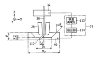
- FIG. 6 is a diagram illustrating the configuration of the protrusion length determination circuit 38 and the protrusion length detection ring 40. Here, the protruding length L T of the wire tail 110 projecting from the capillary 28 is shown.
- the protrusion length detection ring 40 attached to the bonding head 18 is an annular member disposed coaxially with the capillary 28.
- the annular opening of the protrusion length detection ring 40 has a constant inner diameter at first from the ⁇ Z direction to the + Z direction, that is, upward from the bonding stage 14, and then the inner diameter gradually increases. It has a mortar shape.
- the outer diameter of the protrusion length detection ring 40 is D 2 O
- the height as a dimension in the Z direction is H R.
- the inner diameter in the range from the bottom surface, which is the end in the ⁇ Z direction, to the height H I is D I , and the inner diameter gradually increases with an inclination of the angle ⁇ toward the upper surface side.
- the outer diameter D O is about 4 mm
- the total height H R is about 1 mm
- the height H I of the uniform inner diameter portion is about 0.2 mm
- the uniform inner diameter D I is about 2.5 mm and the angle ⁇ is about 45 degrees.
- an appropriate metal material processed into a predetermined shape can be used as the protrusion length detection ring 40.
- the capillary 28 moves in the same manner with respect to the movement in the XY plane, but takes a fixed position with respect to the movement of the capillary 28 in the Z direction. That is, the central axis of the annular opening of the protrusion length detection ring 40 is arranged so as to coincide with the longitudinal axis of the capillary 28, and the capillary 28 extends along the central axis of the annular opening of the protrusion length detection ring 40. Move in the Z direction. When wire bonding is performed at the first bond point 100 and the second bond point 102, the tip of the capillary 28 is in the ⁇ Z direction with respect to the bottom surface of the protruding length detection ring 40.
- the capillary 28 When the protrusion length is determined, the capillary 28 is pulled up in the + Z direction. 6, the tip position of the capillary 28 when the protruding length determination is carried out, is shown from the upper end of the uniform inner diameter D I portion of the protruding length detection ring 40 as the height H G.
- the height H G the wire 30 is extended above the wire tail 110 projecting from the distal end of the capillary 28, to enter the range of the height H I of uniform internal diameter D I portion of the protruding length detection ring 40.
- the protrusion length determination circuit 38 detects the presence / absence of energization when a predetermined inspection voltage is applied between the protrusion length detection ring 40 and the wire 30 and the presence / absence of a discharge spark when a predetermined inspection high voltage is applied therebetween. based on the detection of the judges appropriateness of the protruding length L T of the wire tail 110 projecting from the distal end of the capillary 28.
- the protrusion length determination circuit 38 includes an inspection high voltage 112 and a detection unit 114. One terminal is connected to the protrusion length detection ring 40, and the other terminal is connected to the wire clamper 32.
- the inspection high voltage 112 is a DC voltage, and the detection unit 114 detects a current value.
- the current value in the detection unit 114 does not detect.
- the detecting unit 114 detects a sudden pulse current value.
- the detection portion 114 energization is confirmed .
- a projection length L T of the wire tail 110 projecting from the distal end of the capillary 28 is constant.
- the protruding length L T of the wire tail 110 projecting from the distal end of the capillary 28 has a variation, the projecting length L T of generally normal wire tail 110 Compared to this, the length tends to be longer.
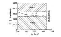
- FIG. 7 is a diagram showing the relationship between the inspection high voltage at which spark discharge occurs and the wire length L L.
- the horizontal axis of FIG. 7 is a wire length L L, the vertical axis represents the test high voltage H V.
- the inspection high voltage at which spark discharge occurs is indicated by characteristic line 116. As shown by the characteristic line 116, when the wire length L L becomes shorter the higher the testing high voltage H V necessary to produce the spark discharge, the wire length L L becomes longer necessary to produce a spark discharge testing high voltage H V decreases.
- the characteristic line 116 determine the test high voltage H V corresponding to the wire length L L, if set as test high voltage 112 of the protruding length determination circuit 38, the projection length if occurred spark discharge L T is appropriate and the normal state shown in FIG. Conversely, if the way the spark discharge under test high voltage 112 which is set is Shojire, inadequate protruding length L T, wire 30 between the first bonding point 100 and the second bonding point 102 It can be determined that the disconnection has occurred.
- the inspection high voltage H V is too high, the protruding length L T is thus cause spark discharge even when the proper protruding length. That is, at the inspection high voltage, it is erroneously detected whether the protrusion length is appropriate.
- the detection region erroneously this, in the example of FIG. 7, a region where the false detection when the H V is equal to or greater than 3300V.
- the region shown in FIG. 7 as being capable of detecting cutting is when the wire length L L is sufficiently long.
- the wire length L L is sufficiently long, there is a margin in the shape of the loop formed between the first bond point 100 and the second bond point 102, and even if the second bond point 102 is not attached, the wire 30 By pulling the wire, there is a margin until the wire 30 is cut. Therefore, before the wire 30 is cut, the non-stick determination circuit 36 can determine non-stick at the second bond point 102.
- the wire length L L is 1000 ⁇ m or more, this is a region where cutting can be detected.
- Characteristic line 116 such erroneous detection area, non-detection region, surrounded by the cut detectable regions, depending on the projected length L T of the wire tail 110 in a region where spark discharge occurs, appropriate protrusion This is a characteristic line obtained by connecting the values of the inspection high voltage at which the spark discharge does not occur when the length is long and the spark discharge is generated when the appropriate protrusion length is exceeded.
- the computer 60 controls the operation of each element of the wire bonding apparatus 10 as a whole.
- the computer 60 includes a control unit 80 that is a CPU, a control unit 80, various interface circuits, and a memory 82. These are connected to each other by an internal bus.
- the various interface circuits are drive circuits or buffer circuits provided between the control unit 80, which is a CPU, and each element of the wire bonding apparatus 10.
- the interface circuit is simply indicated as I / F.
- Various interface circuits include an XY stage I / F 62 connected to the XY stage 16, a Z motor I / F 64 connected to the Z motor 20, an ultrasonic vibrator I / F 66 connected to the ultrasonic vibrator 26, and a clamper opening / closing.
- the memory 82 is a storage device that stores various programs and various control data.
- the various programs include a first bonding program 84 related to the first wire bonding process, a second bonding program 86 related to the second wire bonding process, a movement processing program 88 related to the capillary moving process for wire cutting, and a cutting related to the wire 30 cutting determination process.
- the control data 98 is, for example, detection relation data relating to the wire protrusion length, the inspection high voltage, and the presence / absence of spark described with reference to FIG.
- FIG. 8 is a flowchart showing a wire bonding procedure as a method for manufacturing a semiconductor device.
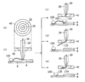
- FIG. 9 is a diagram showing the contents of three determination procedures in the flowchart of FIG. 10 and 11 are diagrams showing the presence or absence of spark discharge in the protrusion length detection ring 40.
- FIG. 8 is a flowchart showing a wire bonding procedure as a method for manufacturing a semiconductor device.
- FIG. 9 is a diagram showing the contents of three determination procedures in the flowchart of FIG. 10 and 11 are diagrams showing the presence or absence of spark discharge in the protrusion length detection ring 40.
- FIG. 8 is a flowchart showing the procedure of wire bonding, and each procedure corresponds to the processing procedure of each program stored in the memory 82 of the computer 60.
- the bonding stage 14 is pulled out once, and the circuit board 8 on which the semiconductor chip 6 as a bonding target is mounted is positioned and set on the bonding stage 14 and is pressed and fixed by the wind clamper 50.
- the bonding stage 14 is returned to the initial position again.
- the bonding stage 14 is heated to a predetermined temperature determined by the bonding conditions.
- This bonding object setting step is automatically performed using an automatic transfer device for the circuit board 8.
- the first bonding program 84 is executed by the control unit 80, and the first wire bonding process is performed at the first bond point 100 (S10).
- the first wire bonding process first, the wire 30 is inserted into the capillary 28 with the wire clamper 32 opened, and the wire 30 protrudes from the tip of the capillary 28. Then, the XY stage 16 and the Z motor 20 are driven to move through the XY stage I / F 62 and the Z motor I / F 64 according to a command from the control unit 80, and the capillary 28 in a state in which the wire 30 protrudes from the tip is formed at the first bond point. Move towards 100.
- the first bond point 100 is set on one lead of the circuit board 8.
- the first bond point 100 is set using a positioning camera or the like not shown in FIG.
- the wire 30 is sandwiched and pressed between the tip of the capillary 28 and the lead of the circuit board 8, and an ultrasonic transducer is passed through the ultrasonic transducer I / F 66 according to a command from the control unit 80. 26 is operated, and the wire 30 and the lead are joined by the ultrasonic vibration energy, the pressing force of the capillary 28 by the drive control of the Z motor 20, and the heating temperature from the bonding stage 14. In this way, the first wire bonding process at the first bond point 100 is performed.
- a loop forming process is performed. That is, after the first wire bonding process is completed, the capillary 28 is lifted upward with the wire clamper 32 open, and then moved directly above the second bond point 102. The second bond point 102 is set on one pad of the semiconductor chip 6. During the movement of the capillary 28, the wire 30 is drawn out from the wire spool 33 and extended from the tip of the capillary 28 by a necessary wire length. The capillary 28 is moved by moving and driving the XY stage 16 and the Z motor 20 according to a command from the control unit 80.
- a second wire bonding process is performed (S12). This processing procedure is performed by the control unit 80 executing the second bonding program 86.
- the loop forming process procedure may be included in the second bonding program 86, and the second wire bonding process may be included including the loop forming process.
- the wire 30 is sandwiched and pressed between the tip of the capillary 28 and the pad of the semiconductor chip 6, and the ultrasonic transducer I is commanded by the control unit 80.
- the ultrasonic vibrator 26 is operated via the / F 66, and the wire 30 and the pad are connected by the ultrasonic vibration energy, the pressing force of the capillary 28 by the drive control of the Z motor 20, and the heating temperature from the bonding stage 14. The space is joined. In this way, the second wire bonding process at the second bond point 102 is performed.
- a movement process for cutting the wire is performed (S14). This processing procedure is performed when the control unit 80 executes the movement processing program 88.
- the movement process for wire cutting is performed as follows.
- the Z motor 20 is rotationally controlled via the Z motor I / F 64 by the command of the control unit 80 to slightly raise the capillary 28.
- the wire tail is pulled obliquely upward, and further, a clamper opening / closing I / F 68 according to a command from the control unit 80
- the clamper opening / closing unit 34 is given a command to close the wire clamper 32.
- the XY stage 16 is driven to move through the XY stage I / F 62, thereby moving the capillary 28 in the XY plane.
- the wire 30 is pulled in the XY plane while the wire 30 is sandwiched between the wire clampers 32. Since the condition of the second wire bonding process is set so that the bonding strength at the second bond point 102 is sufficiently larger than the breaking strength of the wire 30, the wire 30 is cut at the second bond point 102.
- S16 When the movement process of the capillary 28 for cutting the wire is performed, it is determined whether or not the wire is cut (S16). This processing procedure is performed by the control unit 80 executing the cutting determination processing program 90. Whether or not the wire has been cut is determined by operating the non-sticking determination circuit 36 via the cutting determination circuit I / F 70 according to a command from the control unit 80 and receiving the result by the control unit 80. In S16, when it is determined that the wire 30 is not cut, an abnormal signal is output because there is a non-bonding at the second bond point 102 (S26). Even if it is determined in S16 that the wire 30 has been cut, if the bonding is normally performed at the second bond point 102 as it is, an erroneous determination may be made as described with reference to FIG.
- the determination of the protruding length L T is performed for wire tail 110 projecting from the distal end of the capillary 28 (S18). Determination of the protruding length L T is performed using the projected length determination circuit 38 and the protruding length detector ring 40. Determination of the protruding length L T is whether energized wire tail 110 projecting from the distal end of the capillary 28 is in contact with the projecting length detection ring 40 is not detected and (S20), when the current is not detected, a predetermined inspection height This is performed in two steps, whether or not a discharge spark is not detected under voltage (S22). These processing procedures are performed by the control unit 80 executing the protrusion length determination processing program.
- the non-bonding determination at the second bond point 102 is performed through the three-stage determination of S16, S20, and S22, it is determined that the wire 30 has been cut in S16, and it is determined that the energization is not detected in S20. If it is determined in S22 that no discharge spark is detected, it is determined that the second wire bonding at the second bond point 102 has been performed normally and the wire 30 has been cut normally at the second bond point 102 (S24). .
- FIG. 9 shows the state of the three-stage determination regarding the non-stick determination at the second bond point 102.
- FIGS. 9A and 9B are a cross-sectional view and a plan view showing the positional relationship between the capillary 28 and the protruding length detection ring 40 when the second wire bonding process is performed.
- FIG. 9C is a diagram showing a case where the bonding at the second bond point 102 is normally performed and the wire 30 is normally cut at the second bond point 102, and the determination of S16 in FIG. 8 is affirmed. Sometimes corresponds.
- the protrusion length of the wire tail 120 protruding from the tip of the capillary 28 becomes an appropriate protrusion length, and a predetermined inspection high voltage is applied between the wire 30 and the protrusion length detection ring 40 in the wire clamper 32, A discharge spark is not generated between the wire tail 120 protruding from the tip of the capillary 28 and the protruding length detection ring 40.
- FIG. 9D shows a wire tail 122 protruding from the tip of the capillary 28 when the wire 30 is not attached at the second bond point 102 and the wire 30 is cut between the first bond point 100 and the second bond point 102. it is when the projection length L T is too long. At this time, the wire tail 122 protruding from the tip of the capillary 28 is in contact with the protrusion length detection ring 40, and the protrusion length determination circuit 38 detects energization. The determination of S20 in FIG. 8 is denied. Sometimes corresponds.
- FIG. 9E shows a wire tail 124 protruding from the tip of the capillary 28 when the wire 30 is not attached at the second bond point 102 and the wire 30 is cut between the first bond point 100 and the second bond point 102.
- protruding length L T of is when exceeding a suitable projection length a predetermined.
- a predetermined inspection high voltage is applied between the wire 30 and the protrusion length detection ring 40 in the wire clamper 32
- the gap between the wire tail 124 protruding from the tip of the capillary 28 and the protrusion length detection ring 40 is detected.
- Discharge spark occurs in That is, this corresponds to the case where the protrusion length determination circuit 38 detects discharge spark and the determination in S22 in FIG. 9 is negative.
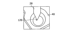
- FIG. 10 and 11 show examples of the presence or absence of discharge between the wire tail protruding from the tip of the capillary 28 and the protruding length detection ring 40 when a predetermined inspection high voltage is set in the protruding length determination circuit 38.
- FIG. FIG. The predetermined inspection high voltage is a wire in an appropriate protruding length range obtained in advance based on various setting conditions such as a wire length and a wire diameter between the first bond point 100 and the second bond point 102 of wire bonding. without protruding length L T in the discharge sparks tail occurs, the protruding length L T exceeds the appropriate protruding length discharge spark is set to occur.
- Figure 10 corresponds to the case of FIG. 9 (c), when the protrusion length L T of the wire tail 120 projecting from the distal end of the capillary 28 is an appropriate protruding length protruding wire tail 120 projecting from the distal end of the capillary 28 There is no discharge spark between the long detection ring 40 and the discharge.
- the tip of FIG. 9 corresponds to the case of (e), when the protrusion length L T of the wire tail 124 projecting from the distal end of the capillary 28 exceeds a suitable projection length corresponding to the check high voltage, capillary 28 A discharge spark 126 is generated between the wire tail 124 protruding from the protrusion and the protruding length detection ring 40.
- the protrusion length detection ring 40 and the protrusion length determination circuit 38 together with the non-bonding determination circuit 36, even if an aluminum wire having a smaller extensibility than a gold wire is used for wedge bonding by the capillary 28, the second bond The non-delivery at the point 102 can be accurately determined.
- FIG. 12 is a diagram showing that the abandoned bonding process is performed between the first wire bonding and the second wire bonding, and is a partial view of the bonding stage 14 viewed from the capillary 28 side in the ⁇ Z direction. is there.
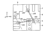
- five leads 7 of the circuit board 8 leads 9 used for discarding bonds, and five pads 5 of the semiconductor chip 6 are shown.
- the first bond point 100 provided on the lead 7 of the circuit board 8 and the second bond point 102 provided on the pad 5 of the semiconductor chip 6 are connected by the wire 130.
- the second wire bonding is performed by connecting a wire 136 between the first bond point 132 provided on the lead 7 of the circuit board 8 and the second bond point 134 provided on the pad 5 of the semiconductor chip 6. is there.
- the connection direction of the wire 130 and the connection direction of the wire 136 have an angle difference of about 70 degrees from each other.
- Bonding point 107 discarded provided leads 9, even protruding length L T of the wire tail 122 projecting from the second bonding point 102 in the capillary 28 of the wire 130 in the first wire bonding unsuitable, second This is the position where the abandoned bond is made so that a smooth transition to wire bonding is possible.
- the abandon bond is performed before the processing at the second bond point 102 of the first wire bonding is completed and the processing of the first bond point 132 of the second wire bonding is started.
- the discard bond process (S27) is performed next.
- This processing procedure is performed by the control unit 80 executing the discard bond program 95.
- the capillary 28 is moved via the XY stage I / F 62 and the Z motor I / F 64, the wire clamper 32 is opened / closed via the clamper opening / closing I / F 68, and the ultrasonic transducer I / F 66 is passed through. Then, the ultrasonic transducer 26 is operated, and this is performed as follows.
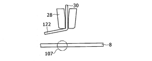
- FIG. 13 is a diagram showing that the capillary 28 has moved just above the discarded bond point 107 of the circuit board 8.
- FIG. 14 is a diagram showing that the wire tail 122 and the circuit board 8 are joined at the discarded bond point 107.
- the capillary 28 is then moved to + Z immediately above the disposal bond point 107 with the wire clamper 32 closed as a wire tail operation and a wire cut operation. Raise in the direction. Since the condition of the discard bond process is set so that the bonding strength at the discard bond point 107 is sufficiently larger than the breaking strength of the wire 30, the wire 30 is cut at the discard bond point 107. As described above, by moving the capillary 28, the wire 30 is discarded and pulled from the bond point 107, and the wire 30 is cut.
- the capillary 28 is moved by a predetermined distance in the XY plane direction from the state of FIG. 14 and is raised obliquely upward indicated by Z 2 in the + Z direction, and the wire 30 is discarded and becomes a cut state 128 at the bond point 107.
- FIG. FIG. 15 shows the portion remaining on the side of the discarded bond point 107 and the wire tail 140 protruding from the tip of the capillary 28.
- the protruding length of the wire tail protruding from the tip of the capillary 28 L T Can be made suitable, and is suitable for the next wire bonding process.
- the discard bond process (S27) is performed immediately after the output of the abnormal signal, but the discard bond process may be performed after the wire bonding apparatus 10 is stopped (S28).
- the end (END) is made after the wire bonding apparatus 10 is stopped (S28), but the next wire bonding process may be directly performed.
- the present invention can be used in a wire bonding apparatus and a wire bonding method for performing wire bonding using a capillary.
Landscapes
- Wire Bonding (AREA)
Abstract
ワイヤボンディング装置(10)は、ワイヤ(30)を挿通するキャピラリ(28)と、ボンディング対象物とクランプ状態のワイヤ(30)との間に所定の電気信号を印加し、その応答に基づいてボンディング対象物とワイヤ(30)との間の不着とワイヤ(30)が切断されたか否かを判定する不着判定回路(36)と、キャピラリ(28)と同軸に配置される円環状の突出長検出リング(40)と、突出長検出リング(40)とワイヤ(30)との間に所定の検査電圧を印加したときの導通の有無の検出およびその間に所定の検査高電圧を印加したときの放電スパークの有無の検出に基づき、キャピラリ(28)の先端から突き出るワイヤテールの突出長の適不適を判定する突出長判定回路(38)とを備える。
Description
本発明は、キャピラリを用いてワイヤボンディングを行うワイヤボンディング装置及び半導体装置の製造方法に関する。
ワイヤボンディング装置は、例えば、基板のリードと半導体チップのパッドとの間を細線のワイヤで接続するために用いられる。ワイヤボンディングは、次のようにして行われる。すなわち、ワイヤボンディング用のツールと共にワイヤをリードに向かって下降させる。最初は高速で下降させ、リードに近づいたら低速にする。この低速下降は第1サーチ(1stサーチ)と呼ばれる。そして、ツール先端でワイヤをリードに押し付け、超音波振動を加えながら両者を接合させて第1ボンド(1stボンド)とする。第1ボンドの後はツールを引き上げてワイヤを延出し、適当なループを形成しながらパッドの上方に移動する。パッドの上方に来るとツールを下降させる。最初は高速で下降させ、パッドに近づいたら低速にする。この低速下降が第2サーチ(2ndサーチ)である。そして、ツール先端でワイヤをパッドに押し付け、超音波振動を加えながら両者を接合させて第2ボンド(2ndボンド)を行う。第2ボンドの後は、ワイヤクランパでワイヤの移動を止めながらツールを引き上げてワイヤを第2ボンド点のところで切断する。これを繰り返して、基板の複数のリードと半導体チップの複数のパッドとの間の接続が行われる。なお、第1ボンド、第2ボンドのときに、適当な加熱を行ってもよい。なお、パッドについて第1ボンドを行い、リードについて第2ボンドを行うものとしてもよい。
このように、ワイヤボンディングにおいては第1ボンドと第2ボンドの2つの接合が行われるが、この第1ボンドや第2ボンドが正常に行われないことがある。また、第1ボンドが不十分で第2ボンドに移るループ形成の段階等でリードからワイヤが剥がれることがあり、また、第1ボンドが正常でもループ形成の途中でワイヤが切断されてしまうこともある。これらの現象をまとめて不着と呼ぶことにすると、不着検出を早期に行う必要がある。不着検出には、基板側とツールのワイヤ側との間に電圧を印加し、あるいは電流を流して、その間の抵抗成分、ダイオード成分、容量成分が正常か否かで判断することが行われる(例えば、特許文献1,2)。
ところで、ワイヤボンディングの方式としては、ボールボンディング方式とウェッジボンディング方式が知られている。
ボールボンディング方式は、高電圧スパーク等でFAB(Free Air Ball)を形成できる金線等を用い、ツールとしては、その長手方向軸の周りについて回転対称形のチャンファ部を先端に有するキャピラリを用いる。ここでは、ワイヤの先端の方向に関わらずFABを方向性のない球形とするために、ワイヤ先端を囲むようにリング状とした高電圧放電電極を用いることが提案されている(例えば、特許文献3)。
ウェッジボンディング方式は、アルミニウム線等を用いてFABを形成せず、ボンディング用のツールとしてキャピラリではなく、ワイヤガイドと押圧面を先端に有するウェッジボンディング用のツールを用いる。ウェッジボンディングでは、ツール先端において、ワイヤガイドに沿ってワイヤを斜めに押圧面側に出し、押圧面でワイヤ側面をボンディング対象物に押し付けてボンディングする。したがって、ツールの先端で押圧面からワイヤが横向きに出る形となり、ツールの先端はその長手方向軸の周りについて回転対称形になっていない(例えば、特許文献4)。
ウェッジボンディング用のツールの先端は回転対称形になっていないので、パッド、リードの配置によっては、そのままではワイヤガイドの方向がワイヤの接続方向と合わないことが生じる。そのために、ツールを保持するボンディングヘッドを回転式にし(例えば、特許文献5)、あるいは、ボンディング対象物を保持するボンディングステージを回転することが行われる。そこで、先端が回転対称形であるキャピラリを用い、キャピラリ先端でワイヤ側面を押圧して接合する方法が提案されている(例えば特許文献6)。
ウェッジボンディング方式では、金線に比べて延伸性が小さいアルミニウムワイヤを用いる。そこで、第1ボンド点におけるワイヤボンディングが正常に行われた後で第2ボンド点におけるワイヤボンディングが不十分で不着となり、そのままワイヤをクランプしてワイヤ切断が行われると、第1ボンド点と第2ボンド点との間のループのところでワイヤが切断されることが生じ得る。
ワイヤの不着や切断は、ボンディング対象物とワイヤとの間に電気信号を与えてその応答から判断できる。しかし、第2ボンド点におけるワイヤボンディングの不着判断が行われる前に、第1ボンド点と第2ボンド点との間のループのところでワイヤが切断されると、ボンディング対象物とワイヤとの間に通電がない点では、第2ボンド点におけるワイヤボンディングが正常で第2ボンド点でワイヤが正常に切断された場合と同じである。したがって、第2ボンド点におけるボンディングの後で不着と切断についての判断を行うと、第2ボンド点におけるボンディングが不着で第1ボンド点と第2ボンド点との間のループのところでワイヤが切断された場合を、第2ボンド点におけるボンディングが正常でワイヤの切断も正常に行われた、と誤判断することになる。
第2ボンド点におけるボンディングが不着で第1ボンド点と第2ボンド点との間のループのところでワイヤが切断されると、ボンディング用のツールの先端から長いワイヤが突き出る状態となる。この状態が、第2ボンド点におけるワイヤボンディングが正常と誤判断されると、この状態のまま、次のボンディング処理が行われる。つまり、ボンディング用のツールの先端から長いワイヤが突き出る状態で、次の第1ボンド点におけるワイヤボンディングが行われることになり、不良品が発生する。このように、第2ボンド点におけるボンディングが正常か否かについて誤判断が生じると、不良品発生の原因となる。
本発明の目的は、第2ボンド点におけるボンディングが正常か否かについて、的確な判断を行うことができるワイヤボンディング装置及び半導体装置の製造方法を提供することである。
本発明に係るワイヤボンディング装置は、ワイヤを挿通するキャピラリと、キャピラリと同軸に配置される円環状のワイヤ突出長検出リングと、ワイヤ突出長検出リングとワイヤとの間に所定の検査電圧を印加したときの通電の有無の検出に基づき、キャピラリの先端から突き出るワイヤの突出長の適不適を判定する突出長判定部と、を備える。
また、本発明に係るワイヤボンディング装置は、通電は、ワイヤ突出長検出リングとワイヤとの間に所定の検査電圧を印加して非導通状態であると検出したならば、ワイヤ突出長検出リングとワイヤとの間に所定の検査高電圧を印加して放電スパークの有無の検出をするとしても好適である。
また、本発明に係るワイヤボンディング装置は、突出長判定部は、ワイヤの突出長と検査高電圧とスパークの有無に関する検出関係を予め求めておき、ワイヤボンディングのボンディング条件に応じて検査高電圧を設定し、ボンディング条件に適したワイヤの突出長か否かを判定するとしても好適である。
また、本発明に係るワイヤボンディング装置は、第1ボンド点におけるワイヤボンディングに引き続き第2ボンド点におけるワイヤボンディングを行った後、ワイヤをクランプ状態としてキャピラリを移動することでワイヤを第2ボンド点から切断する処理を行った後に、ボンディング対象物とクランプ状態のワイヤとの間に所定の電気信号を印加し、その応答に基づいてワイヤが切断されたか否かを判定する切断判定部を備え、突出長判定部は、切断判定部においてワイヤが切断されていると判定した場合に、ワイヤの突出長の適不適を判定し、ワイヤの突出長が不適のときに、第1ボンド点におけるボンディングが行われず、第1ボンド点と第2ボンド点との間でワイヤが切断されたとして異常信号を出力するとしても好適である。
また、本発明に係るワイヤボンディング装置は、ワイヤの突出長が不適と判定されたとき、予め定めた捨てボンド点を用いて、ワイヤの切断された先端部分を適切な突出長にする捨てボンド処理部を備えるとしても好適である。
また、本発明に係るワイヤボンディング装置は、第1ボンド点および第2ボンド点におけるワイヤボンディングは、ウェッジボンディング方式で行われるとしても好適である。
また、本発明に係る半導体装置の製造方法は、ワイヤボンディングの第1ボンド点において、ワイヤを挿通するキャピラリを用いてウェッジボンディング方式で第1ボンディング対象物とワイヤとの間を接合する第1ワイヤボンディング処理工程と、第1ボンド点におけるワイヤボンディングの後、第1ボンド点から所定のワイヤ長でワイヤを延出し、ワイヤボンディングの第2ボンド点において、第2ボンディング対象物とワイヤとの間を接合する第2ワイヤボンディング処理工程と、第2ボンド点におけるワイヤボンディングの後、ワイヤを第2ボンド点から切断するために、ワイヤをクランプ状態として、ワイヤを挿通しているキャピラリを移動する移動処理工程と、ワイヤの切断のためのキャピラリの移動を行った後に、第2ボンディング対象物とワイヤとの間に所定の電気信号を印加し、その応答に基づいてワイヤが切断されたか否かを判定する切断判定処理工程と、ワイヤが切断されていると判定した場合に、キャピラリと同軸に配置される円環状のワイヤ突出長検出リングとワイヤとの間に所定の検査電圧を印加したときの通電の有無の検出に基づき、キャピラリの先端から突き出るワイヤの突出長の適不適を判定する突出長判定工程と、ワイヤの突出長が不適のときに、第2ボンド点におけるボンディングを行わず、第1ボンド点と第2ボンド点との間でワイヤが切断されたとして異常信号を出力する出力処理工程と、を有する。
また、本発明に係る半導体装置の製造方法は、通電は、ワイヤ突出長検出リングとワイヤとの間に所定の検査電圧を印加して非導通状態であると検出したならば、ワイヤ突出長検出リングとワイヤとの間に所定の検査高電圧を印加して放電スパークの有無の検出をするとしても好適である。
また、本発明に係る半導体装置の製造方法は、ワイヤの突出長が不適と判定されたとき、予め定めた捨てボンド点を用いて、ワイヤの切断された先端部分を適切な突出長にする捨てボンド処理工程を有するとしても好適である。
本発明に係るワイヤボンディング装置及び半導体装置の製造方法によれば、第2ボンド点におけるボンディングが正常か否かについて、正しい判断を行うことができる。
以下に図面を用いて本発明に係る実施の形態を詳細に説明する。以下において、ワイヤボンディングの対象物として、第1ボンド点では回路基板のリード、第2ボンド点では半導体チップのパッドとして述べるが、これは説明のための例示であって、第1ボンド点を半導体チップのパッドとし、第2ボンド点を回路基板のリードとしてもよい。第1ボンド点と第2ボンド点をともに半導体チップのパッドとしてもよく、第1ボンド点と第2ボンド点をともに回路基板のリードとしてもよい。パッド、リードはワイヤが接合される対象物の例示であって、これ以外のものであってもよい。また、ボンディングの対象物としては、半導体チップの他、抵抗チップ、コンデンサチップ等の一般的な電子部品でもよく、回路基板としては、エポキシ樹脂基板等の他、リードフレーム等であってもよい。
以下で述べる寸法、材質等は、説明のための例示であって、ワイヤボンディング装置の仕様に応じ、適宜変更が可能である。
以下では、全ての図面において一または対応する要素には同一の符号を付し、重複する説明を省略する。
図1は、ワイヤボンディング装置10の構成図である。このワイヤボンディング装置10は、ワイヤボンディング用のツールとしてキャピラリ28を用い、ワイヤ30としてアルミニウム線を用い、ウェッジボンディング方式で、2つのボンディング対象物をワイヤ30で接続する装置である。図1では、ワイヤボンディング装置10の構成要素ではないが、ボンディング対象物としての半導体チップ6と回路基板8が示されている。なお、本発明の実施の形態において、ウェッジボンディング方式とは、ワイヤ先端にFABを形成せず、超音波、圧力を用いて行うボンディング方式をいう。
ワイヤボンディング装置10は、架台12に保持されるボンディングステージ14と、XYステージ16と、コンピュータ60を含んで構成される。
ボンディングステージ14は、2つのボンディング対象物である半導体チップ6と回路基板8とを搭載するボンディング対象物保持台である。ボンディングステージ14は、回路基板8等を搭載または排出する際に、架台12に対して移動可能であるが、ボンディング処理の間は架台12に対し固定状態とされる。かかるボンディングステージ14としては、金属製の移動テーブルを用いることができる。ボンディングステージ14は、ワイヤボンディング装置10の接地電位等の基準電位に接続される。ボンディングステージ14は、後述する不着判定回路36の接地側端子に接続される。半導体チップ6や回路基板8との間の絶縁が必要な場合には、ボンディングステージ14の必要な部分に絶縁処理が設けられる。
半導体チップ6は、シリコン基板にトランジスタ等を集積化して電子回路としたもので、電子回路としての入力端子と出力端子等が半導体チップ6の上面に複数のパッド(図示せず)として引き出されている。半導体チップ6の下面はシリコン基板の裏面で、電子回路の接地電極とされる。
回路基板8は、エポキシ樹脂基板に所望の配線をパターニングしたもので、半導体チップ6の下面を電気的および機械的に接続して固定するチップパッド(図示せず)と、その周囲に配置される複数のリード(図示せず)と、チップパッドや複数のリードから引き出された回路基板としての入力端子と出力端子を有する。ワイヤボンディングは、半導体チップ6のパッドと、回路基板8のリードとの間をワイヤ30で接続することで行われる。
ボンディングステージ14に設けられるウィンドクランパ50は、中央部に開口を有する平板状の部材で、回路基板8を保持する部材である。ウィンドクランパ50は、中央部の開口の中にワイヤボンディングが行われる回路基板8のリードと半導体チップ6とが配置されるように位置決めして、開口の周縁部で回路基板8を押さえることで、回路基板8をボンディングステージ14に固定する。
後述するようにワイヤ30の突出長が不適切に切断されたときに、次の工程のために捨てボンド処理が行われる。
XYステージ16は、ボンディングヘッド18を搭載し、架台12およびボンディングステージ14に対し、ボンディングヘッド18をXY平面内の所望の位置に移動させる移動台である。XY平面は、架台12の上面と平行な平面である。Y方向は、後述するボンディングアーム(図示せず)に取り付けられた超音波トランスデューサ24の長手方向に平行な方向である。図1に、X方向、Y方向と、XY平面に垂直な方向であるZ方向を示した。
ボンディングヘッド18は、XYステージ16に固定されて搭載され、Zモータ20を内蔵し、その回転制御によってZ駆動アーム22、超音波トランスデューサ24を介して、キャピラリ28をZ方向に移動させる移動機構である。Zモータ20としては、リニアモータを用いることができる。
Z駆動アーム22は、超音波トランスデューサ24と、ワイヤクランパ32とが取り付けられ、Zモータ20の回転制御によって、ボンディングヘッド18に設けられる回転中心の周りに回転可能な部材である。ボンディングヘッド18に設けられる回転中心は、必ずしもZモータ20の出力軸ではなく、Z駆動アーム22、超音波トランスデューサ24、ワイヤクランパ32を含めた全体の重心位置を考慮し、回転負荷が軽減される位置に設定される。
超音波トランスデューサ24は、根元部がZ駆動アーム22に取り付けられ、先端部にワイヤ30を挿通するキャピラリ28が取り付けられる細長い棒部材である。超音波トランスデューサ24には超音波振動子26が取り付けられ、超音波振動子26を駆動することで発生する超音波エネルギをキャピラリ28に伝達する。したがって、超音波トランスデューサ24は、超音波振動子26からの超音波エネルギを効率よくキャピラリ28に伝達できるように、先端側に行くほど先細りとなるホーン形状に形成される。超音波振動子26としては、圧電素子が用いられる。
キャピラリ28は、先端面が平らな円錐体で、ワイヤ30を長手方向に沿って挿通させることができる貫通孔を中心部に有するボンディングツールである。かかるキャピラリ28としては、ボールボンディングに用いられるセラミック製のキャピラリをそのまま用いることができる。ボールボンディングに用いられるキャピラリは、FABを保持しやすいように、貫通孔の先端面側に適当なチャンファと呼ばれる隅部形状が設けられているが、本実施の形態のウェッジボンディング方式では、ボールボンディング用のキャピラリを用い、このキャピラリの貫通孔の先端面側の下面にフェイスと呼ばれる平面を備える。このフェイスが、ワイヤボンディング装置10においてウェッジボンディングを行うときの押圧面となる。
ウェッジボンディング用のツールは、先端部に、長手方向に対し斜めに設けられるワイヤガイドと、ワイヤの側面を押圧するための押圧面を有するので、ツールの長手方向軸の周りに回転対称でなく、ワイヤは、ワイヤガイドの方向に沿った方向性を有して横方向に突き出す。このようなウェッジボンディング用のツールを用いると、リード、パッドの配置によっては、そのままではワイヤガイドの方向がワイヤの接続方向と合わないことが生じる。
例えば、回路基板8の中央部に半導体チップ6が搭載され、半導体チップ6の周辺部に沿って一周するように複数のパッドが配置され、回路基板8にも、半導体チップ6の外側に沿って一周するように複数のリードが設けられる場合には、リードとパッドとを結ぶワイヤの接続方向が複数のワイヤボンディングのそれぞれによって異なる。ワイヤガイドの方向をワイヤの接続方向に合わせるには、ウェッジボンディング用のツールを長手方向軸の周りに回転させるか、回路基板8を回転させる必要がある。
これに対し、キャピラリ28の先端面側のフェイスは、キャピラリ28の長手方向軸の周りに回転対称の形状であるので、パッドとリードとを結ぶワイヤの接続方向が各ワイヤボンディングごとに異なっても、キャピラリ28の先端から突き出るワイヤ30の方向を少し変更する整形処理を行うだけで済む。このため、ウェッジボンディングにキャピラリ28を用いる。
キャピラリ28に挿通されるワイヤ30は、アルミニウムの細線である。ワイヤ30は、ボンディングヘッド18から延びるワイヤホルダの先端に設けられるワイヤスプール33に巻回され、ワイヤスプール33からワイヤクランパ32を介してキャピラリ28の中心部の貫通孔に挿通されて、キャピラリ28の先端から突き出る。かかるワイヤ30の材質としては、純アルミニウム細線の他に、シリコン、マグネシウム等を適当に混合させた細線等を用いることができる。ワイヤ30の直径は、ボンディング対象物によって選択することができる。ワイヤ30の直径の一例を挙げると、30μmである。
ワイヤクランパ32は、Z駆動アーム22に取り付けられ、ワイヤ30の両側に配置される1組の挟み板で、向かい合う挟み板の間を開くことでワイヤ30を自由移動状態とし、向かい合う挟み板の間を閉じることで、ワイヤ30の移動を停止させるワイヤ挟み装置である。ワイヤクランパ32は、Z駆動アーム22に取り付けられるので、キャピラリ28がXYZ方向に移動しても、ワイヤ30を適切に挟むことができる。ワイヤクランパ32の開閉は、圧電素子を用いたクランパ開閉部34の作動によって行われる。
不着判定回路36は、ワイヤボンディングの各段階で、ボンディング対象物とワイヤ30との間の接続が適切か否かを判定する回路である。不着判定回路36は、ボンディング対象物とワイヤ30との間に所定の電気信号を印加し、その応答に基づいて、ボンディング対象物とワイヤ30との間の接続が適切か否かを判定する。
ワイヤボンディングの各段階としては、回路基板8のリードから半導体チップ6のパッドへワイヤ30を接続する場合、回路基板8のリードを第1ボンド点とし、半導体チップ6のパッドを第2ボンド点として、第1ボンド点にワイヤ30を接続する第1ワイヤボンディング処理工程と、第1ボンド点から第2ボンド点に向かってワイヤ30を延出してループを形成するループ形成処理工程と、第2ボンド点にワイヤ30を接続する第2ワイヤボンディング処理工程と、第2ワイヤボンディング処理の後、第2ボンド点においてワイヤ30を切断するためにキャピラリ28を移動させる移動処理工程がある。
不着判定回路36は、第1ボンド点においてワイヤ30とリードが接合しているか否か、第2ボンド点においてワイヤ30とパッドが接合しているか否か、第2ボンド点においてワイヤ30が切断されたか否か等を、それぞれの工程のタイミングで判定する回路である。
ここでは特に、不着判定回路36は、第2ボンド点において第2ワイヤボンディング処理の後でワイヤ30が切断されたか否かを判定する。その意味で、不着判定回路36は、切断判定回路と呼ぶことができる。
図2は、不着判定回路36が切断判定回路として機能するときを示す図である。図2では、第1ワイヤボンディング処理工程で、第1ボンド点100において適切にワイヤボンディングが行われたことが確認され、その後、ワイヤ30のループ形成処理工程を経て、第2ワイヤボンディング処理工程に移行し、第2ワイヤボンディング処理工程も第2ボンド点102において適切にワイヤボンディングが行われたことが確認され、次に、キャピラリ28の移動処理工程が行われ、第2ボンド点102において、ワイヤ30が切断状態104となっていることを示す図である。
不着判定回路36は、印加電源106と測定部108から構成され、一方端子はボンディングステージ14に接続され、他方端子は、ワイヤクランパ32またはワイヤスプール33に接続される。印加電源106を直流電圧電源として、測定部108の内部に図示しないインピーダンス測定回路によりインピーダンス値を測定することで、ワイヤ30とボンディングステージ14の間の抵抗成分が分かる。印加電源106を交流電圧電源として、測定部108の内部に図示しないインピーダンス測定回路によりインピーダンス値を測定することで、ワイヤ30とボンディングステージ14の間の容量成分が分かる。
ワイヤボンディングにおいて、直流または交流による着・不着の検査は、対象となるデバイスにより異なり、また同一デバイスであってもパッドごとに異なる。直流電圧電源を印加する場合で、ワイヤ30が半導体チップ6のパッドと接続状態(着状態)にあるときは、抵抗成分が有限値となる。交流電圧電源を印加する場合は、ワイヤ30が半導体チップ6のパッドと接続状態(着状態)にあるときと非接続状態(不着状態)にあるときとでは容量成分に大きな差が発生する。交流電圧電源を印加して、ワイヤ30が半導体チップ6のパッドと接続状態(着状態)にあるときは、非接続状態(不着状態)に比べて大きな容量成分となる。一方、直流電圧電源を印加する場合で、ワイヤ30が切断状態104のときは、ワイヤ30とボンディングステージ14との間が電気的に開放状態になるので、抵抗成分が無限大になる。また、交流電圧電源を印加する場合で、ワイヤ30が半導体チップ6のパッドと切断状態(不着状態)にあるときは、接続状態(着状態)に比べ小さい容量成分となる。このように、測定部108における抵抗成分または容量成分の変化に基づいて、不着判定回路36は、ワイヤ30とボンディングステージ14との間が接続状態か開放状態かを判定でき、これによってワイヤ30が切断状態104であるか否かを判定することができる。
突出長判定回路38と突出長検出リング40は、不着判定回路36において、ワイヤ30が切断状態であると判断されたときに、その切断状態が、図2で説明したように、第2ボンド点102におけるワイヤボンディングが正常で、ワイヤ30が第2ボンド点102において切断されたものであるか否かを判断するために設けられる。
これは、第2ワイヤボンディング処理が不適切でワイヤ30が第2ボンド点102において不着状態であって、ワイヤ30が第1ボンド点100と第2ボンド点102の間で切断されても、ワイヤ30とボンディングステージ14との間は開放状態であるので、不着判定回路36は、ワイヤ30が着状態の第2ボンド点102において切断されたと誤判定してしまう可能性があるからである。
これについて、図3を用いて説明する。図3は、不着判定回路36の判定のタイミングとワイヤ切断のタイミングによっては、不着判定回路36の結果をそのまま受け取ると、誤判定が生じ得ることを説明する図である。
図3(a)から(c)は、第2ボンド点102における第2ワイヤボンディング処理が正常に行われ、切断のための移動処理によってワイヤ30が第2ボンド点102で正常に切断された場合を示す図である。
図3(a)は、時間t=t0で第2ボンド点102における第2ワイヤボンディング処理が終了し、キャピラリ28が+Z方向に少し上昇した状態を示している。ここでは、第2ワイヤボンディング処理が正常に行われ、第2ボンド点102でワイヤ30と半導体チップ6のパッドとの間が正常に接合されている。図3(b)は、時間t=t1で、キャピラリ28がワイヤ切断のためにXY平面内で所定の移動を行った状態を示している。所定の移動として、ここでは、キャピラリ28が+X方向にX1移動した状態が示されている。このt=t1で、第2ボンド点102のところでワイヤ30が正常に切断状態103となっている。図3(c)は、キャピラリ28がさらに+X方向にX3の位置まで移動した後の時間t=t4の状態を示す図である。
この場合、第2ボンド点102における不着判定は、t=t0とt=t4における不着判定回路36の判定結果に基づいて行うことができる。すなわち、t=t0でワイヤ30が切断されてなく、t=t4でワイヤ30が切断状態であるときには、第2ボンド点102でワイヤ30の接合が正常に行われ、そして第2ボンド点102においてワイヤ30が正常に切断されたとし、t=t0でワイヤ30が切断されてなく、t=t4でもワイヤ30が切断されていないときは、第2ボンド点102でワイヤ30が不着状態で、そのままワイヤ30が切断されていない、と判定することができる。
図3(d)から(f)は、第2ワイヤボンディング処理が不適切で第2ボンド点102においてワイヤ30と半導体チップ6のパッドとの間が接合されずに不着となり、ワイヤ30が第1ボンド点100と第2ボンド点102との間で切断された場合を示す図である。
図3(d)は、(a)と同じく第2ワイヤボンディング処理が終了してキャピラリ28が+Z方向に少し上がったときであるが、ここでは第2ワイヤボンディング処理が正常に行われず、ワイヤ30と半導体チップ6のパッドが接合せず、不着状態となっている。図3(e)は、第2ワイヤボンディング処理が正常に行われた際と同様に、キャピラリ28が+X方向にX2だけ移動したことで、第1ボンド点100と第2ボンド点102との間でワイヤ30が切断状態105となったことを示す。図3(f)は、キャピラリ28が更に+X方向にX3の位置まで移動した後の時間t=t4の状態を示す図である。図3(f)のt4,X3は、図3(c)と同じである。なお、X1<X2<X3である。ここで第2ボンド点102は、ワイヤ30とパッドとの間が不着となっているが、予定では第2ワイヤボンディング処理が行われる点を指す。
このときに、第2ボンド点102における不着判定について、t=t0とt=t4における不着判定回路36の判定結果に基づいて行うと、誤判定をすることになる。すなわち、t=t0ではワイヤ30が切断されてなく、t=t4でワイヤ30が切断状態であり、これは、図3(a)から(c)で説明した正常処理の場合と同じ状態である。したがって、t=t0とt=t4における不着判定回路36の判定結果に基づいて第2ボンド点102における不着判定を行うと、図3(a)から(c)の正常処理の場合と、図3(d)から(f)の不着の場合を区別できず、誤判定を行うことになる。
図3(a)から(c)の正常処理の場合と、図3(d)から(f)の不着の場合の相違は、t=t1の図3(b)とt=t2の図3(e)である。したがって、図3(a)から(c)の正常処理の場合と、図3(d)から(f)の不着の場合を不着判定回路36で区別しようとすると、t=t1とt=t2の間で、ワイヤ30の切断が生じたか否かを判定する必要がある。t=t1とt=t2は、ループ形状やカット速度等の影響を受けるので、ワイヤボンディングのパラメータ変更の都度変わることになる。t=t1とt=t2の間が十分長ければ、不着判定回路36は、図3(a)から(c)の場合と図3(d)から(f)の場合を区別し得るが、t=t1とt=t2の間が短いと、この2つの場合を誤判定する可能性が高くなる。
図4は、ワイヤボンディング条件として、第1ボンド点100と第2ボンド点102との間の距離が短く、その間に形成されるループの高さが低く、またループ長が短い場合である。このように短く低いループが形成される場合には、第2ボンド点102が不着のときに、ワイヤ30が早めに切断されやすく、図3におけるt=t1とt=t2との差がなく、上記2つの場合を誤判定する可能性が高くなる。
図4(a)は、図3(d)のt=t0よりやや早めのタイミングで、第2ワイヤボンディング処理が終了してキャピラリ28が+Z方向に少し上がりかけたときの状態である。ここでは、第2ボンド点102で不着状態となっている。図4(b)は、t=t1で、図4(a)からキャピラリ28が+Z方向に少し上がり、X方向にX1移動したときで、ワイヤ30はまだ切断されていない。図4(c)は、t=t2で、キャピラリ28は+X方向にX4まで移動し、ここでワイヤ30は第1ボンド点100と第2ボンド点102との間で切断状態105となった。図4は、短く低いループが形成される場合であるので、図4(c)に示す時刻t2,X4は、図3(e)の時刻t2,X2より短く、小さな値であり、早い時間でワイヤ30が切断される。
図5は、ワイヤボンディング条件として、第1ボンド点100と第2ボンド点102との間の距離が長く、その間に形成されるループの高さが高く、またループ長が長い場合である。このように長く高いループが形成される場合には、第2ボンド点102が不着のときでも、ワイヤ30の切断までに時間的余裕があり、図3におけるt=t1とt=t2が長くなり、上記2つの場合を誤判定する可能性が低くなる。
図5(a)は、t=t0の状態で、図4(a)と同じく第2ワイヤボンディング処理が終了してキャピラリ28が+Z方向に少し上がりかけたときの状態である。ここでも第2ボンド点102で不着状態である。図5(b)は、t=t1で、図4(b)と同じく、図5(a)からキャピラリ28が+Z方向に少し上がり、X方向にX1移動したときであるが、図4(b)に比べループが高く形成されている。このとき、ワイヤ30はまだ切断されていない。図5(c)は、t=t3で、キャピラリ28は+X方向にX5まで移動したときである。X=X5は、図3(c),(f)のt=t3におけるX=X3よりも大きく、また、t=t3、X=X5は、図4(c)のt=t2、X=X4よりも長く、大きな値である。ここでもワイヤ30はまだ切断されていない。このように、長く高いループが形成される場合には、第2ボンド点102において不着状態であっても、ワイヤ30が切断されるまでに時間的に余裕があり、上記2つの場合を誤判定する可能性が低くなる。なお、図3から図5に示す+X方向への各移動距離の関係は、X1<X4<X2<X3<X5の通りである。
このように、短く低いループが形成される場合ほど、不着判定回路36は上記2つの場合を区別できなくなる。突出長判定回路38と突出長検出リング40は、この2つの場合を的確に区別する。
ワイヤ30が第2ボンド点102で切断された場合には、キャピラリ28の先端から突き出るワイヤ30の突出長が短く、適切な値となる。これに対し、ワイヤ30が第1ボンド点100と第2ボンド点102の間で切断された場合には、キャピラリ28の先端から突き出るワイヤ30の突出長が長く、不適切な値となる。突出長判定回路38と突出長検出リング40は、キャピラリ28の先端から突き出るワイヤ30の突出長が適切か否かを判定し、これによって、不着判定回路36が判定できない2つの場合を区別する。
図6は、突出長判定回路38と突出長検出リング40の構成を示す図である。ここでは、キャピラリ28から突き出るワイヤテール110の突出長LTが示されている。
ボンディングヘッド18に取り付けられる突出長検出リング40は、キャピラリ28と同軸に配置される円環状の部材である。突出長検出リング40の円環状の開口部は、-Z方向から+Z方向に向かって、すなわち、ボンディングステージ14から見て上方側に向かって、最初は一定の内径で、その後、次第に内径が広がるすり鉢状の形状を有する。図6の符号を用いて説明すると、突出長検出リング40の外径はDOで、Z方向の寸法である高さはHRである。-Z方向の端部である底面から高さHIの範囲の内径はDIで、それより上面側に向かって、角度αの傾きで、内径が次第に大きくなる。
突出長検出リング40の寸法の一例を挙げると、外径DOは約4mm、全高HRは約1mm、一様内径部分の高さHIは約0.2mm、一様内径DIは約2.5mm、角度αは約45度である。かかる突出長検出リング40は、適当な金属材料を所定の形状に加工したものを用いることができる。
突出長検出リング40はボンディングヘッド18に取り付けられるので、キャピラリ28のXY平面内の移動については同じように移動するが、キャピラリ28のZ方向の移動に対しては固定位置を取る。すなわち、突出長検出リング40の円環状の開口部の中心軸はキャピラリ28の長手方向軸と一致するように配置され、キャピラリ28は突出長検出リング40の円環状の開口部の中心軸に沿ってZ方向に移動する。第1ボンド点100、第2ボンド点102においてワイヤボンディング処理を行っているときは、キャピラリ28の先端は突出長検出リング40の底面よりも-Z方向にある。
突出長判定を行うときは、キャピラリ28は+Z方向に引き上げられる。図6では、突出長判定が行われるときのキャピラリ28の先端位置が、突出長検出リング40の一様内径DI部分の上端から高さHGとして示されている。高さHGは、ワイヤ30がキャピラリ28の先端から突き出るワイヤテール110の延長した先が、突出長検出リング40の一様内径DI部分の高さHIの範囲に入るようにする。このように高さHGを設定することで、突出長検出リング40とワイヤテール110との間の放電スパークの有無検出を的確に行うことができる。
突出長判定回路38は、突出長検出リング40とワイヤ30との間に所定の検査電圧を印加したときの通電の有無の検出およびその間に所定の検査高電圧を印加したときの放電スパークの有無の検出に基づき、キャピラリ28の先端から突き出るワイヤテール110の突出長LTの適不適を判定する。突出長判定回路38は、検査高電圧112と検出部114から構成され、一方端子は突出長検出リング40に接続され、他方端子は、ワイヤクランパ32に接続される。検査高電圧112は、直流電圧で、検出部114は、電流値を検出する。
ワイヤテール110の突出長LTが短いときは、突出長検出リング40とワイヤテール110との間に放電スパークが生じないので、検出部114では電流値が検出されない。ワイヤテール110の突出長LTが適当に長くなると、突出長検出リング40とワイヤテール110との間に放電スパークが生じるので、検出部114では、突発的なパルス状の電流値を検出する。ワイヤテール110の突出長LTが長すぎて突出長検出リング40に接触すると、ワイヤテール110と突出長検出リング40との間が電気的に導通し、検出部114では、通電が確認される。このように、検出部114が検出する電流値によって、ワイヤテール110の突出長LTの長さが判定できる。
図3(a)から(c)のように、第2ワイヤボンディング処理が正常に行われて第2ボンド点102でワイヤ30が切断された場合と、図3(d)から(f)のように、第2ワイヤボンディング処理が不適切であって第2ボンド点102が不着状態のままでワイヤ30が第1ボンド点100と第2ボンド点102との間で切断された場合の2つを区別するには、図3(c)の正常の場合のワイヤテール110の突出長LTを適切突出長として、そのときにはスパーク放電が生じないようにし、適切突出長を超える突出長LTのときにスパーク放電が生じるように、検査高電圧112を設定することがよい。1つのワイヤボンディング処理工程が正常に完了した場合は、キャピラリ28の先端から突き出るワイヤテール110の突出長LTが一定である。これに対し、1つのワイヤボンディング工程で異常が発生した場合は、キャピラリ28の先端から突き出るワイヤテール110の突出長LTはばらつきがあり、一般的に正常なワイヤテール110の突出長LTに比べてその長さが長くなる傾向がある。
図7は、スパーク放電が生じる検査高電圧とワイヤ長LLの関係を示す図である。図7の横軸はワイヤ長LLで、縦軸は検査高電圧HVである。スパーク放電が生じる検査高電圧は特性線116で示される。特性線116に示されるように、ワイヤ長LLが短くなるとスパーク放電を生じさせるのに必要な検査高電圧HVが高くなり、ワイヤ長LLが長くなるとスパーク放電を生じさせるのに必要な検査高電圧HVが低くなる。
したがって、特性線116を用いて、ワイヤ長LLに対応する検査高電圧HVを求め、これを突出長判定回路38の検査高電圧112として設定すれば、スパーク放電が生じなければ突出長LTが適切で、図3(c)に示す正常状態であることになる。反対に、そのようにして設定された検査高電圧112の下でスパーク放電が生じれば、突出長LTが不適切で、第1ボンド点100と第2ボンド点102との間でワイヤ30の切断が生じたものと判断することができる。
なお、検査高電圧HVが高すぎると、突出長LTが適切突出長のときにもスパーク放電を生じさせてしまう。つまり、その検査高電圧では、適切突出長かについて誤検出することになる。これを誤検出する領域とすると、図7の例では、HVが3300V以上となるときが誤検出する領域である。
検査高電圧HVが低すぎると、突出長LTが適切突出長を超えるときにもスパーク放電が生じない。つまり、その検査高電圧では、適切突出長かについて検出することができない。これを不検出の領域とすると、図7の例では、HVが2400V以下となるときが不検出の領域である。
図7で切断検出可能として示される領域は、ワイヤ長LLが十分長いときである。ワイヤ長LLが十分長いときは、第1ボンド点100と第2ボンド点102との間に形成されるループの形状に余裕があり、第2ボンド点102が不着であっても、ワイヤ30を引っ張ることでワイヤ30が切断されるまでに余裕がある。したがって、ワイヤ30が切断される前に、不着判定回路36が第2ボンド点102における不着を判定することができる。図7の例では、ワイヤ長LLが1000μm以上となるときが切断検出可能な領域である。
特性線116は、このような誤検出する領域、不検出の領域、切断検出可能な領域で囲まれ、ワイヤテール110の突出長LTに応じてスパーク放電が生じる領域の中で、適切な突出長のときにはスパーク放電が発生せず、適切な突出長を超えるときにはスパーク放電が発生する検査高電圧の値をつないで得られた特性線である。
再び図1に戻り、コンピュータ60は、ワイヤボンディング装置10の各要素の動作を全体として制御する。コンピュータ60は、CPUである制御部80と、制御部80と、各種のインタフェース回路と、メモリ82を含んで構成される。これらは互いに内部バスで接続される。
各種インタフェース回路は、CPUである制御部80とワイヤボンディング装置10の各要素との間に設けられる駆動回路またはバッファ回路である。図1では、インタフェース回路を単にI/Fとして示した。各種インタフェース回路は、XYステージ16に接続されるXYステージI/F62、Zモータ20に接続されるZモータI/F64、超音波振動子26に接続される超音波振動子I/F66、クランパ開閉部34に接続されるクランパ開閉I/F68、切断判定回路として機能する不着判定回路36に接続される切断回路I/F70、突出長判定回路38に接続される突出長判定回路I/F72である。
メモリ82は、各種プログラムと、各種制御データを格納する記憶装置である。各種プログラムは、第1ワイヤボンディング処理に関する第1ボンディングプログラム84、第2ワイヤボンディング処理に関する第2ボンディングプログラム86、ワイヤ切断のためのキャピラリ移動処理に関する移動処理プログラム88、ワイヤ30の切断判定処理に関する切断判定処理プログラム90、ワイヤ30の突出長判定処理に関する突出長判定処理プログラム92、ワイヤ切断が異常であることを示す異常出力処理に関する異常出力処理プログラム94、異常出力がされたときに次の工程のための捨てボンド処理に関する捨てボンドプログラム95、その他の制御処理に関する制御プログラム96である。制御データ98としては、例えば、図7で説明したワイヤの突出長と検査高電圧とスパーク有無に関する検出関係データ等である。
上記構成の作用、特にコンピュータ60の各機能について、図8以下を用いてさらに詳細に説明する。図8は、半導体装置の製造方法としてのワイヤボンディングの手順を示すフローチャートである。図9は、図8のフローチャートの3つの判断手順の内容を示す図である。図10と図11は、突出長検出リング40におけるスパーク放電の有無を示す図である。
図8は、ワイヤボンディングの手順を示すフローチャートで、各手順は、コンピュータ60のメモリ82に格納される各プログラムの処理手順に対応する。ワイヤボンディング装置10に電源等が投入されると、コンピュータ60を含むワイヤボンディング装置10の各構成要素の初期化が行われる。
次に、ボンディングステージ14が一旦引き出され、ボンディング対象物である半導体チップ6が搭載された回路基板8がボンディングステージ14上に位置決めセットされ、ウィンドクランパ50によって押さえつけられて固定される。ボンディングステージ14は再び初期状態の位置に戻される。なお、ボンディングステージ14は、ボンディング条件で定められた所定の温度に加熱される。このボンディング対象物設定工程は、回路基板8の自動搬送装置を用いて自動的に行われる。
次に、第1ボンディングプログラム84が制御部80によって実行され、第1ボンド点100において第1ワイヤボンディング処理が行われる(S10)。第1ワイヤボンディング処理は、まず、ワイヤクランパ32が開いた状態で、キャピラリ28にワイヤ30が挿通されキャピラリ28の先端にワイヤ30が突き出る状態とされる。そして、制御部80の指令によってXYステージI/F62とZモータI/F64を介して、XYステージ16とZモータ20が移動駆動され、先端にワイヤ30が突き出る状態のキャピラリ28が第1ボンド点100に向かって移動する。第1ボンド点100は、回路基板8の1つのリード上に設定される。第1ボンド点100の設定は、図1では図示されていない位置決めカメラ等を用いて行われる。
第1ボンド点100では、キャピラリ28の先端部と回路基板8のリードとの間にワイヤ30が挟み込んで押し付けられ、制御部80の指令で超音波振動子I/F66を介して超音波振動子26が作動され、その超音波振動エネルギとZモータ20の駆動制御によるキャピラリ28の押圧力と、ボンディングステージ14からの加熱温度とによって、ワイヤ30とリードとの間が接合される。このようにして、第1ボンド点100における第1ワイヤボンディング処理が行われる。
第1ワイヤボンディング処理が終了すると、ループ形成処理が行われる。すなわち、第1ワイヤボンディング処理が終了した後、ワイヤクランパ32を開いた状態でキャピラリ28を上方に上昇させ、次に第2ボンド点102の直上に移動させる。第2ボンド点102は、半導体チップ6の1つのパッド上に設定される。キャピラリ28の移動の間、ワイヤ30は、ワイヤスプール33から繰り出されて、キャピラリ28の先端から必要なワイヤ長だけ延出される。キャピラリ28の移動は、制御部80の指令によってXYステージ16とZモータ20が移動駆動されることで行われる。
ループ形成処理の後、第2ワイヤボンディング処理が行われる(S12)。この処理手順は、制御部80が第2ボンディングプログラム86を実行することで行われる。ループ形成処理手順を第2ボンディングプログラム86に含め、ループ形成処理を含めて第2ワイヤボンディング処理としてもよい。
第2ボンド点102では、第1ワイヤボンディング処理と同様に、キャピラリ28の先端部と半導体チップ6のパッドとの間にワイヤ30が挟み込んで押し付けられ、制御部80の指令で超音波振動子I/F66を介して超音波振動子26が作動され、その超音波振動エネルギとZモータ20の駆動制御によるキャピラリ28の押圧力と、ボンディングステージ14からの加熱温度とによって、ワイヤ30とパッドとの間が接合される。このようにして、第2ボンド点102における第2ワイヤボンディング処理が行われる。
第2ワイヤボンディング処理が終了すると、次にワイヤ切断のための移動処理が行われる(S14)。この処理手順は、制御部80が移動処理プログラム88を実行することで行われる。ワイヤ切断のための移動処理は、次のように行われる。
第2ボンド点102における接合処理が行われた後、制御部80の指令で、ZモータI/F64を介してZモータ20を回転制御してキャピラリ28を少し上昇させる。次に、制御部80の指令で、XYステージI/F62を介してXYステージ16を移動駆動させることにより、ワイヤテールを斜め上方に引き出し、さらに、制御部80の指令で、クランパ開閉I/F68を介してクランパ開閉部34に指令を与えてワイヤクランパ32を閉じ、その状態で、XYステージI/F62を介してXYステージ16を移動駆動させ、これによってキャピラリ28をXY平面内で移動させる。
つまり、ワイヤクランパ32でワイヤ30を挟んだ状態でワイヤ30をXY平面内で引っ張る。第2ボンド点102における接合強度はワイヤ30の破断強度よりも十分大きくなるように第2ワイヤボンディング処理の条件設定が行われているので、ワイヤ30は、第2ボンド点102において切断される。
ワイヤ切断のためのキャピラリ28の移動処理が行われると、ワイヤが切断されたか否かの判定が行われる(S16)。この処理手順は、制御部80が切断判定処理プログラム90を実行することで行われる。ワイヤ切断が行われたか否かは、制御部80の指令で、切断判定回路I/F70を介して不着判定回路36を作動させ、その結果を制御部80が受け取って行われる。S16において、ワイヤ30が切断されていないと判定されるときは、第2ボンド点102における不着があるとして異常信号を出力する(S26)。S16において、ワイヤ30が切断されていると判定したときでも、そのまま第2ボンド点102において正常に接合が行われたとすると、図3で説明したように、誤判定をする可能性がある。
そこで、ワイヤ切断の判定のS16において、ワイヤ30が切断されていると判定されると、次に、キャピラリ28の先端から突き出すワイヤテール110について突出長LTの判定が行われる(S18)。突出長LTの判定は、突出長判定回路38と突出長検出リング40を用いて行われる。突出長LTの判定は、キャピラリ28の先端から突き出すワイヤテール110が突出長検出リング40に接触する通電が検出されなかったか否か(S20)と、通電が検出されないときに、所定の検査高電圧の下で放電スパークが検出されなかったか否か(S22)の2段階で行われる。これらの処理手順は、制御部80が突出長判定処理プログラムを実行することで行われる。
このように、第2ボンド点102における不着判定は、S16,S20,S22の3段階の判定を経て行われ、S16でワイヤ30が切断されたと判定され、S20で通電の検出がされないと判定され、S22で放電スパークが検出されないと判定されると、第2ボンド点102における第2ワイヤボンディングが正常に行われ、ワイヤ30が第2ボンド点102において正常に切断されたと判定される(S24)。
一方、S16でワイヤ30が切断されたとは判定されないときは、第2ボンド点102においてワイヤ30が不着でワイヤ30が切断されていないとされる。S16の判定が肯定でS20において通電が検出されると、第2ボンド点102においてワイヤ不着で、ワイヤ30が第1ボンド点100と第2ボンド点102との間で切断され、キャピラリ28からのワイヤテール110の突出長が適切な突出長をかなり超えて長いと判断される。S20の判定が肯定でS22において放電スパークが検出されると、キャピラリ28からのワイヤテール110の突出長LTが適切な突出長を超えていると判定される。これらの各場合はいずれも異常信号が出力され(S26)、ワイヤボンディング装置10の動作が停止される(S28)。この処理手順は、制御部80が異常出力処理プログラム94を実行することで行われる。
第2ボンド点102における不着判定に関する3段階の判定の様子を図9に示す。図9(a)と(b)は、第2ワイヤボンディング処理を行っているときのキャピラリ28、突出長検出リング40の配置関係を示す断面図と平面図である。
図9(c)は、第2ボンド点102における接合が正常に行われ、ワイヤ30が第2ボンド点102で正常に切断された場合を示す図で、図8におけるS16の判定が肯定されたときに対応する。この場合、キャピラリ28の先端から突き出るワイヤテール120の突出長が適切な突出長となり、ワイヤクランパ32におけるワイヤ30と突出長検出リング40との間に所定の検査高電圧が印加されたときに、キャピラリ28の先端から突き出るワイヤテール120と突出長検出リング40との間に放電スパークが発生しない。
図9(d)は、第2ボンド点102においてワイヤ30が不着で、ワイヤ30が第1ボンド点100と第2ボンド点102との間で切断されて、キャピラリ28の先端から突き出るワイヤテール122の突出長LTが長すぎるときである。このときは、キャピラリ28の先端から突き出るワイヤテール122が突出長検出リング40に接触し、突出長判定回路38が通電の検出をした場合を示す図で、図8におけるS20の判定が否定されたときに対応する。
図9(e)は、第2ボンド点102においてワイヤ30が不着で、ワイヤ30が第1ボンド点100と第2ボンド点102との間で切断されて、キャピラリ28の先端から突き出るワイヤテール124の突出長LTが予め定めた適切な突出長を超えたときである。このときは、ワイヤクランパ32におけるワイヤ30と突出長検出リング40との間に所定の検査高電圧が印加されたときに、キャピラリ28の先端から突き出るワイヤテール124と突出長検出リング40との間に放電スパークが発生する。つまり、突出長判定回路38が放電スパーク検出をした場合で、図9におけるS22の判定が否定されたときに対応する。
図10と図11は、突出長判定回路38において所定の検査高電圧が設定されたときに、キャピラリ28の先端から突き出るワイヤテールと突出長検出リング40との間の放電の有無の例を示す図である。所定の検査高電圧は、ワイヤボンディングの第1ボンド点100から第2ボンド点102との間のワイヤ長やワイヤ径等の各種設定条件に基づいて予め求められた適切な突出長の範囲のワイヤテールの突出長LTでは放電スパークが発生せず、適切な突出長を超す突出長LTでは放電スパークが発生するように設定される。
図10は、図9(c)の場合に対応し、キャピラリ28の先端から突き出るワイヤテール120の突出長LTが適切な突出長であるときで、キャピラリ28の先端から突き出るワイヤテール120と突出長検出リング40との間で放電スパークが発生していない。
図11は、図9(e)の場合に対応し、キャピラリ28の先端から突き出るワイヤテール124の突出長LTが検査高電圧に対応する適切な突出長を超えたときで、キャピラリ28の先端から突き出るワイヤテール124と突出長検出リング40との間で放電スパーク126が発生している。
このように、不着判定回路36と共に、突出長検出リング40と突出長判定回路38を用いることで、キャピラリ28によるウェッジボンディングに金線より展伸性が小さいアルミニウム線を用いても、第2ボンド点102における不着を的確に判定することができる。
上記では、S26で異常信号出力がされると、S28でワイヤボンディング装置10の動作が停止されるものとした。異常信号出力がされるときは、キャピラリ28の先端から突き出るワイヤテールの突出長LTが不適となっている。そこで、S26とS28の間に捨てボンド処理(S27)を行い、ワイヤ30の突出長を適切なものにすることがよい。捨てボンド処理は、制御部80が捨てボンドプログラム95を実行することで行われる。捨てボンド処理は、回路基板8のリードの中で適当な広さを有するものを捨てボンド用のリードとして用いてもよく、また、半導体チップ6においても、製品として実害の無い部分であれば、捨てボンドを行う場所や位置は限定されない。以下では、捨てボンド処理を行う例として、図9(d)のワイヤテール122について、その突出長LTを適切化する場合について述べる。
図12は、1つ目のワイヤボンディングと2つ目のワイヤボンディングの間に捨てボンド処理が行われることを示す図で、ボンディングステージ14をキャピラリ28の側から-Z方向に見た部分図である。ここでは、回路基板8の5つのリード7と、捨てボンドに用いられるリード9と、半導体チップ6の5つのパッド5が示されている。
ここで、1つ目に行われるワイヤボンディングは、回路基板8のリード7に設けられる第1ボンド点100と、半導体チップ6のパッド5に設けられる第2ボンド点102の間をワイヤ130によって接続するものである。2つ目に行われるワイヤボンディングは、回路基板8のリード7に設けられる第1ボンド点132と、半導体チップ6のパッド5に設けられる第2ボンド点134の間をワイヤ136によって接続するものである。ワイヤ130の接続方向と、ワイヤ136の接続方向は、互いに約70度の角度の差を有する。
リード9に設けられる捨てボンド点107は、1つ目のワイヤボンディングにおけるワイヤ130の第2ボンド点102でキャピラリ28から突き出るワイヤテール122の突出長LTが不適であっても、2つ目のワイヤボンディングにスムーズに移行できるように、捨てボンドが行われる位置である。捨てボンドは、1つ目のワイヤボンディングの第2ボンド点102での処理が終了して、2つ目のワイヤボンディングの第1ボンド点132の処理が開始する前に行われる。
すなわち図8において、異常信号出力処理(S26)が行われると、次に捨てボンド処理(S27)が行われる。この処理手順は、制御部80が捨てボンドプログラム95を実行することで行われる。捨てボンド処理は、XYステージI/F62とZモータI/F64を介してキャピラリ28を移動させ、クランパ開閉I/F68を介して、ワイヤクランパ32を開閉させ、超音波振動子I/F66を介して超音波振動子26を作動させて、次のようにして行われる。
キャピラリ28の先端からワイヤテール122が突き出るワイヤ30を保持して、捨てボンド用のリード9に設けられた捨てボンド点107の直上にキャピラリ28を移動する。図13は、回路基板8の捨てボンド点107の直上にキャピラリ28が移動したことを示す図である。
次に、ワイヤテール122を先端に保持した状態でキャピラリ28を-Z方向に下降させ、捨てボンド点107においてワイヤボンディングを行う。すなわち、制御部80の指令で超音波振動子I/F66を介して超音波振動子26が作動され、その超音波振動エネルギとZモータ20の駆動制御によるキャピラリ28の押圧力と、必要に応じては、ボンディングステージ14からの加熱温度とによって、ワイヤテール122と回路基板8のリード9との間が接合される。図14は、捨てボンド点107において、ワイヤテール122と回路基板8との間が接合されることを示す図である。
捨てボンド点107においてワイヤテール122と回路基板8とが接合されると、次に、ワイヤテール動作およびワイヤカット動作として、ワイヤクランパ32を閉じた状態でキャピラリ28を捨てボンド点107から直上に+Z方向に上昇させる。捨てボンド点107における接合強度はワイヤ30の破断強度よりも十分大きくなるように捨てボンド処理の条件設定が行われているので、ワイヤ30は、捨てボンド点107において切断される。このようにキャピラリ28の移動処理によって、ワイヤ30が捨てボンド点107から引っ張られて、ワイヤ30の切断が行われる。
図15は、図14の状態から、キャピラリ28がXY平面方向に所定距離移動し+Z方向にZ2と示される斜め上方に上昇され、ワイヤ30が捨てボンド点107のところで切断状態128となったことを示す図である。図15には、捨てボンド点107の側に残った部分と、キャピラリ28の先端から突き出るワイヤテール140が示される。
このように、キャピラリ28の先端から突き出るワイヤテールの突出長LTが不適で異常信号出力がされるときでも、捨てボンド処理を行うことで、キャピラリ28の先端から突き出るワイヤテールの突出長LTを適切なものにでき、次のワイヤボンディング処理に適した状態となる。図8のフローチャートには、捨てボンド処理(S27)を異常信号出力の直後に行われるように書いたが、捨てボンド処理をワイヤボンディング装置10の停止(S28)の後に行ってもよい。さらに、図8のフローチャートには、ワイヤボンディング装置10の停止(S28)の後は終了(END)としたが、そのまま次のワイヤボンディング処理に進んでもよい。
本発明は、以上説明した実施形態に限定されるものではなく、請求の範囲により規定されている本発明の技術的範囲ないし本質から逸脱することのない全ての変更及び修正を包含するものである。
本発明は、キャピラリを用いてワイヤボンディングを行うワイヤボンディング装置およびワイヤボンディング方法に利用できる。
5 パッド、6 半導体チップ、7,9 リード、8 回路基板、10 ワイヤボンディング装置、12 架台、14 ボンディングステージ、16 XYステージ、18 ボンディングヘッド、20 Zモータ、22 Z駆動アーム、24 超音波トランスデューサ、26 超音波振動子、28 キャピラリ、30,130,136 ワイヤ、32 ワイヤクランパ、33 ワイヤスプール、34 クランパ開閉部、36 不着判定回路、38 突出長判定回路、40 突出長検出リング、50 ウィンドクランパ、60 コンピュータ、62 XYステージI/F、64 ZモータI/F、66 超音波振動子I/F、68 クランパ開閉I/F、70 切断判定回路I/F、72 突出長判定回路I/F、80 制御部、82 メモリ、84 第1ボンディングプログラム、86 第2ボンディングプログラム、88 移動処理プログラム、90 切断判定処理プログラム、92 突出長判定処理プログラム、94 異常出力処理プログラム、95 捨てボンドプログラム、96 制御プログラム、98 制御データ、100,132 第1ボンド点、102,134 第2ボンド点、103,104,105,128 切断状態、106 印加電源、107 捨てボンド点、108 測定部、110,120,122,124,140 ワイヤテール、112 検査高電圧、114 検出部、116 特性線、126 放電スパーク。
Claims (9)
- ワイヤを挿通するキャピラリと、
前記キャピラリと同軸に配置される円環状のワイヤ突出長検出リングと、
前記ワイヤ突出長検出リングと前記ワイヤとの間に所定の検査電圧を印加したときの通電の有無の検出に基づき、前記キャピラリの先端から突き出る前記ワイヤの突出長の適不適を判定する突出長判定部と、
を含む、ワイヤボンディング装置。 - 請求項1に記載のワイヤボンディング装置であって、
前記通電は、前記ワイヤ突出長検出リングと前記ワイヤとの間に所定の検査電圧を印加して非導通状態であると検出したならば、前記ワイヤ突出長検出リングと前記ワイヤとの間に所定の検査高電圧を印加して放電スパークの有無の検出をする、ワイヤボンディング装置。 - 請求項1に記載のワイヤボンディング装置であって、
前記突出長判定部は、
前記ワイヤの突出長と前記検査高電圧と前記スパークの有無に関する検出関係を予め求めておき、ワイヤボンディングのボンディング条件に応じて前記検査高電圧を設定し、前記ボンディング条件に適した前記ワイヤの突出長か否かを判定する、ワイヤボンディング装置。 - 請求項3に記載のワイヤボンディング装置であって、
第1ボンド点におけるワイヤボンディングに引き続き第2ボンド点におけるワイヤボンディングを行った後、前記ワイヤをクランプ状態として前記キャピラリを移動することで前記ワイヤを前記第2ボンド点から切断する処理を行った後に、ボンディング対象物と前記クランプ状態の前記ワイヤとの間に所定の電気信号を印加し、その応答に基づいて前記ワイヤが切断されたか否かを判定する切断判定部を備え、
前記突出長判定部は、前記切断判定部において前記ワイヤが切断されていると判定した場合に、前記ワイヤの突出長の適不適を判定し、前記ワイヤの突出長が不適のときに、前記第2ボンド点におけるボンディングが行われず、前記第1ボンド点と前記第2ボンド点との間で前記ワイヤが切断されたとして異常信号を出力する、ワイヤボンディング装置。 - 請求項4に記載のワイヤボンディング装置であって、
ワイヤの突出長が不適と判定されたとき、予め定めた捨てボンド点を用いて、ワイヤの切断された先端部分を適切な突出長にする捨てボンド処理部を備える、ワイヤボンディング装置。 - 請求項4または5に記載のワイヤボンディング装置であって、
前記第1ボンド点および前記第2ボンド点における前記ワイヤボンディングは、ウェッジボンディング方式で行われる、ワイヤボンディング装置。 - ワイヤボンディングの第1ボンド点において、ワイヤを挿通するキャピラリを用いてウェッジボンディング方式で第1ボンディング対象物と前記ワイヤとの間を接合する第1ワイヤボンディング処理工程と、
前記第1ボンド点における前記ワイヤボンディングの後、前記第1ボンド点から所定のワイヤ長で前記ワイヤを延出し、前記ワイヤボンディングの前記第2ボンド点において、第2ボンディング対象物と前記ワイヤとの間を接合する第2ワイヤボンディング処理工程と、
前記第2ボンド点における前記ワイヤボンディングの後、前記ワイヤを前記第2ボンド点から切断するために、前記ワイヤをクランプ状態として、前記ワイヤを挿通しているキャピラリを移動する移動処理工程と、
前記ワイヤの切断のための前記キャピラリの移動を行った後に、前記第2ボンディング対象物と前記ワイヤとの間に所定の電気信号を印加し、その応答に基づいて前記ワイヤが切断されたか否かを判定する切断判定処理工程と、
前記ワイヤが切断されていると判定した場合に、前記キャピラリと同軸に配置される円環状のワイヤ突出長検出リングと前記ワイヤとの間に所定の検査電圧を印加したときの通電の有無の検出に基づき、前記キャピラリの先端から突き出る前記ワイヤの突出長の適不適を判定する突出長判定工程と、
前記ワイヤの突出長が不適のときに、前記第2ボンド点におけるボンディングを行わず、前記第1ボンド点と前記第2ボンド点との間で前記ワイヤが切断されたとして異常信号を出力する出力処理工程と、
を有する、半導体装置の製造方法。 - 請求項7に記載の半導体装置の製造方法であって、
前記通電は、前記ワイヤ突出長検出リングと前記ワイヤとの間に所定の検査電圧を印加して非導通状態であると検出したならば、前記ワイヤ突出長検出リングと前記ワイヤとの間に所定の検査高電圧を印加して放電スパークの有無の検出をする、半導体装置の製造方法。 - 請求項7に記載の半導体装置の製造方法であって、
ワイヤの突出長が不適と判定されたとき、予め定めた捨てボンド点を用いて、ワイヤの切断された先端部分を適切な突出長にする捨てボンド処理工程を有する、半導体装置の製造方法。
Priority Applications (4)
| Application Number | Priority Date | Filing Date | Title |
|---|---|---|---|
| CN201380034229.0A CN104395995B (zh) | 2012-11-16 | 2013-06-27 | 打线装置及半导体装置的制造方法 |
| SG11201503763PA SG11201503763PA (en) | 2012-11-16 | 2013-06-27 | Wire-bonding apparatus and method of manufacturing semiconductor device |
| KR1020147028499A KR101596249B1 (ko) | 2012-11-16 | 2013-06-27 | 와이어 본딩 장치 및 반도체 장치의 제조 방법 |
| US14/709,761 US9368471B2 (en) | 2012-11-16 | 2015-05-12 | Wire-bonding apparatus and method of manufacturing semiconductor device |
Applications Claiming Priority (2)
| Application Number | Priority Date | Filing Date | Title |
|---|---|---|---|
| JP2012252210A JP5426000B2 (ja) | 2012-11-16 | 2012-11-16 | ワイヤボンディング装置及びワイヤボンディング方法 |
| JP2012-252210 | 2012-11-16 |
Related Child Applications (1)
| Application Number | Title | Priority Date | Filing Date |
|---|---|---|---|
| US14/709,761 Continuation US9368471B2 (en) | 2012-11-16 | 2015-05-12 | Wire-bonding apparatus and method of manufacturing semiconductor device |
Publications (1)
| Publication Number | Publication Date |
|---|---|
| WO2014076997A1 true WO2014076997A1 (ja) | 2014-05-22 |
Family
ID=49052465
Family Applications (1)
| Application Number | Title | Priority Date | Filing Date |
|---|---|---|---|
| PCT/JP2013/067592 Ceased WO2014076997A1 (ja) | 2012-11-16 | 2013-06-27 | ワイヤボンディング装置及び半導体装置の製造方法 |
Country Status (7)
| Country | Link |
|---|---|
| US (1) | US9368471B2 (ja) |
| JP (1) | JP5426000B2 (ja) |
| KR (1) | KR101596249B1 (ja) |
| CN (1) | CN104395995B (ja) |
| SG (1) | SG11201503763PA (ja) |
| TW (1) | TWI539541B (ja) |
| WO (1) | WO2014076997A1 (ja) |
Families Citing this family (21)
| Publication number | Priority date | Publication date | Assignee | Title |
|---|---|---|---|---|
| CN103069557B (zh) * | 2010-08-10 | 2015-12-02 | 库力索法工业公司 | 引线环、形成引线环的方法及相关处理 |
| JP5426000B2 (ja) * | 2012-11-16 | 2014-02-26 | 株式会社新川 | ワイヤボンディング装置及びワイヤボンディング方法 |
| US9165842B2 (en) * | 2014-01-15 | 2015-10-20 | Kulicke And Soffa Industries, Inc. | Short tail recovery techniques in wire bonding operations |
| TWI517277B (zh) * | 2014-02-14 | 2016-01-11 | 新川股份有限公司 | 打線裝置以及半導體裝置的製造方法 |
| TWI557821B (zh) * | 2014-02-21 | 2016-11-11 | 新川股份有限公司 | 半導體裝置的製造方法以及打線裝置 |
| TWI555104B (zh) * | 2014-09-11 | 2016-10-21 | 矽品精密工業股份有限公司 | 打線裝置及排除不良銲線之方法 |
| JP5950994B2 (ja) * | 2014-12-26 | 2016-07-13 | 株式会社新川 | 実装装置 |
| TWI643276B (zh) * | 2016-08-23 | 2018-12-01 | Shinkawa Ltd. | 夾線裝置的校準方法以及打線裝置 |
| US10600756B1 (en) * | 2017-02-15 | 2020-03-24 | United States Of America, As Represented By The Secretary Of The Navy | Wire bonding technique for integrated circuit board connections |
| KR102375893B1 (ko) * | 2017-10-24 | 2022-03-17 | 삼성디스플레이 주식회사 | 유기 발광 표시 장치 및 유기 발광 표시 장치의 제조 방법 |
| JP7077650B2 (ja) * | 2018-02-16 | 2022-05-31 | トヨタ自動車株式会社 | ボンディング装置、及びボンディング方法 |
| EP3887085B1 (en) * | 2018-11-28 | 2024-03-13 | Kulicke and Soffa Industries, Inc. | Ultrasonic welding systems and methods of using the same |
| JP6973831B2 (ja) * | 2019-03-08 | 2021-12-01 | 株式会社新川 | ワイヤボンディング装置 |
| US11420287B2 (en) * | 2019-09-29 | 2022-08-23 | Ningbo Shangjin Automation Technology Co., Ltd. | Wire clamping system for fully automatic wire bonding machine |
| KR102793253B1 (ko) | 2020-05-14 | 2025-04-08 | 삼성전자주식회사 | 반도체 패키지의 와이어 본딩 방법 |
| CN114453753A (zh) * | 2022-01-26 | 2022-05-10 | 芜湖固高自动化技术有限公司 | 一种电阻片自动焊接设备 |
| TWI848292B (zh) * | 2022-05-20 | 2024-07-11 | 日商新川股份有限公司 | 打線接合系統、打線接合檢查裝置、打線接合方法以及電腦程式產品 |
| CN115621141A (zh) * | 2022-10-13 | 2023-01-17 | 重庆平创半导体研究院有限责任公司 | 一种铝线键合方法 |
| JP7515216B1 (ja) * | 2023-06-16 | 2024-07-12 | 株式会社新川 | ワイヤボンディング装置及びリカバリ方法 |
| US20250162060A1 (en) * | 2023-11-21 | 2025-05-22 | Kulicke And Soffa Industries, Inc. | Wire bonding systems, wire replacement systems, and related methods |
| US20250201765A1 (en) * | 2023-12-15 | 2025-06-19 | Kulicke And Soffa Industries, Inc. | Methods of operating wire bonding systems, including methods of detecting and/or preventing wire fly-out on such systems |
Citations (3)
| Publication number | Priority date | Publication date | Assignee | Title |
|---|---|---|---|---|
| JPH1056034A (ja) * | 1996-08-12 | 1998-02-24 | Hitachi Ltd | ボンディング装置 |
| JP2005332850A (ja) * | 2004-05-18 | 2005-12-02 | Kaijo Corp | ワイヤボンディング装置 |
| JP2012023080A (ja) * | 2010-07-12 | 2012-02-02 | Denso Corp | ワイヤボンディング方法 |
Family Cites Families (28)
| Publication number | Priority date | Publication date | Assignee | Title |
|---|---|---|---|---|
| JPS557415A (en) | 1978-06-30 | 1980-01-19 | Toyo Kagaku Sangyo Kk | Faucet molding mold in fiber reinforcing plastic material |
| US4213556A (en) * | 1978-10-02 | 1980-07-22 | General Motors Corporation | Method and apparatus to detect automatic wire bonder failure |
| US4422568A (en) | 1981-01-12 | 1983-12-27 | Kulicke And Soffa Industries, Inc. | Method of making constant bonding wire tail lengths |
| JPS5834938A (ja) * | 1981-08-27 | 1983-03-01 | Nec Corp | ボンデイング装置 |
| US4586642A (en) * | 1985-05-13 | 1986-05-06 | Kulicke And Soffa Industries Inc. | Wire bond monitoring system |
| JP2817314B2 (ja) | 1990-02-15 | 1998-10-30 | 松下電器産業株式会社 | ワイヤボンダおよびワイヤボンディング方法 |
| JP2814154B2 (ja) * | 1991-04-16 | 1998-10-22 | 株式会社新川 | ボンデイング装置 |
| JP3192761B2 (ja) * | 1992-06-17 | 2001-07-30 | 芝浦メカトロニクス株式会社 | ワイヤボンディング方法 |
| US5302836A (en) * | 1992-07-16 | 1994-04-12 | Bernard Siu | High speed image acquisition for microelectronics inspection |
| JP2714339B2 (ja) * | 1993-01-19 | 1998-02-16 | ローム株式会社 | ワイヤボンディング装置 |
| US5402927A (en) * | 1994-06-09 | 1995-04-04 | Kulicke And Soffa Investments, Inc. | Adjustable wire tensioning apparatus |
| JP3335043B2 (ja) | 1995-03-27 | 2002-10-15 | 株式会社カイジョー | 半導体デバイスの状態判定方法及び状態判定装置 |
| US5645210A (en) * | 1996-02-09 | 1997-07-08 | Kulicke And Soffa Investments, Inc. | High speed bonding tool contact detector |
| JP2000137026A (ja) * | 1998-10-30 | 2000-05-16 | Suzuki Motor Corp | 異常検査方法およびワイヤボンディング装置の接合良否検査システム |
| JP3201371B2 (ja) * | 1999-02-02 | 2001-08-20 | 日本電気株式会社 | ワイヤボンディング装置 |
| US6082657A (en) * | 1999-02-11 | 2000-07-04 | Powerchip Semiconductor Corp. | Wire-feeding device using logical circuitry and multiple sensors |
| JP2000306940A (ja) | 1999-04-21 | 2000-11-02 | Shinkawa Ltd | バンプボンディングにおける不着検査方法及び装置 |
| JP2001189340A (ja) * | 1999-12-28 | 2001-07-10 | Shinkawa Ltd | ワイヤボンデイング方法及びその装置 |
| DE10061691B4 (de) * | 2000-12-12 | 2004-12-30 | Agie S.A., Losone | Vorrichtung und Verfahren zur Detektion einer Bearbeitungselektrode einer Werkzeugmaschine |
| SG106126A1 (en) * | 2002-03-08 | 2004-09-30 | Esec Trading Sa | Method and apparatus for dispensing solder on a substrate |
| TWI248186B (en) | 2004-01-09 | 2006-01-21 | Unaxis Internat Tranding Ltd | Method for producing a wedge-wedge wire connection |
| JP4530984B2 (ja) * | 2005-12-28 | 2010-08-25 | 株式会社新川 | ワイヤボンディング装置、ボンディング制御プログラム及びボンディング方法 |
| CN102047400B (zh) * | 2008-03-17 | 2013-01-30 | 库力索法工业公司 | 用于线焊机的导线放线测量和校准技术 |
| US20120032354A1 (en) * | 2010-08-06 | 2012-02-09 | National Semiconductor Corporation | Wirebonding method and device enabling high-speed reverse wedge bonding of wire bonds |
| PH12012000317B1 (en) * | 2011-10-25 | 2014-08-04 | Asm Tech Singapore Pte Ltd | Automatic wire tail adjustment system for wire bonders |
| JP5426000B2 (ja) * | 2012-11-16 | 2014-02-26 | 株式会社新川 | ワイヤボンディング装置及びワイヤボンディング方法 |
| SG11201604465VA (en) * | 2013-12-11 | 2016-07-28 | Fairchild Semiconductor | Integrated wire bonder and 3d measurement system with defect rejection |
| US9165842B2 (en) * | 2014-01-15 | 2015-10-20 | Kulicke And Soffa Industries, Inc. | Short tail recovery techniques in wire bonding operations |
-
2012
- 2012-11-16 JP JP2012252210A patent/JP5426000B2/ja not_active Expired - Fee Related
-
2013
- 2013-04-30 TW TW102115383A patent/TWI539541B/zh not_active IP Right Cessation
- 2013-06-27 CN CN201380034229.0A patent/CN104395995B/zh active Active
- 2013-06-27 SG SG11201503763PA patent/SG11201503763PA/en unknown
- 2013-06-27 WO PCT/JP2013/067592 patent/WO2014076997A1/ja not_active Ceased
- 2013-06-27 KR KR1020147028499A patent/KR101596249B1/ko not_active Expired - Fee Related
-
2015
- 2015-05-12 US US14/709,761 patent/US9368471B2/en not_active Expired - Fee Related
Patent Citations (3)
| Publication number | Priority date | Publication date | Assignee | Title |
|---|---|---|---|---|
| JPH1056034A (ja) * | 1996-08-12 | 1998-02-24 | Hitachi Ltd | ボンディング装置 |
| JP2005332850A (ja) * | 2004-05-18 | 2005-12-02 | Kaijo Corp | ワイヤボンディング装置 |
| JP2012023080A (ja) * | 2010-07-12 | 2012-02-02 | Denso Corp | ワイヤボンディング方法 |
Also Published As
| Publication number | Publication date |
|---|---|
| TW201421591A (zh) | 2014-06-01 |
| KR101596249B1 (ko) | 2016-02-22 |
| JP2013157594A (ja) | 2013-08-15 |
| US20150243627A1 (en) | 2015-08-27 |
| CN104395995A (zh) | 2015-03-04 |
| SG11201503763PA (en) | 2015-06-29 |
| CN104395995B (zh) | 2017-03-15 |
| TWI539541B (zh) | 2016-06-21 |
| KR20140138903A (ko) | 2014-12-04 |
| JP5426000B2 (ja) | 2014-02-26 |
| US9368471B2 (en) | 2016-06-14 |
Similar Documents
| Publication | Publication Date | Title |
|---|---|---|
| JP5426000B2 (ja) | ワイヤボンディング装置及びワイヤボンディング方法 | |
| KR101672510B1 (ko) | 와이어 본딩 장치 및 와이어 본딩 방법 | |
| KR101598999B1 (ko) | 와이어 본딩 장치 및 반도체 장치의 제조 방법 | |
| US8123108B2 (en) | Method of manufacturing semiconductor device and wire bonding apparatus | |
| JP6715402B2 (ja) | ワイヤボンディング方法及びワイヤボンディング装置 | |
| US9899348B2 (en) | Wire bonding apparatus and method of manufacturing semiconductor device | |
| WO2018110417A1 (ja) | ワイヤボンディング装置及びワイヤボンディング方法 | |
| JPH02187286A (ja) | 自動ワイヤ接着装置 | |
| JP4064366B2 (ja) | 超音波フリップチップ接合装置および接合方法 | |
| CN100516826C (zh) | 用于检查楔形接合的质量的方法 | |
| JP6973831B2 (ja) | ワイヤボンディング装置 | |
| JP2722886B2 (ja) | ワイヤボンディング装置 | |
| TWI529831B (zh) | 打線裝置以及打線方法 | |
| US12476219B2 (en) | Wire bonding state determination method and device using a prescribed electric waveform | |
| JPS6231134A (ja) | 超音波ワイヤボンディング方法および装置 | |
| JP2025122515A (ja) | ワイヤボンディング装置、制御装置、及び制御方法 | |
| KR20210033909A (ko) | 와이어 본딩 장치 및 와이어 본딩 방법 |
Legal Events
| Date | Code | Title | Description |
|---|---|---|---|
| 121 | Ep: the epo has been informed by wipo that ep was designated in this application |
Ref document number: 13855623 Country of ref document: EP Kind code of ref document: A1 |
|
| ENP | Entry into the national phase |
Ref document number: 20147028499 Country of ref document: KR Kind code of ref document: A |
|
| NENP | Non-entry into the national phase |
Ref country code: DE |
|
| 122 | Ep: pct application non-entry in european phase |
Ref document number: 13855623 Country of ref document: EP Kind code of ref document: A1 |