WO2014076804A1 - 実装機、及び基準マークの読取方法 - Google Patents
実装機、及び基準マークの読取方法 Download PDFInfo
- Publication number
- WO2014076804A1 WO2014076804A1 PCT/JP2012/079697 JP2012079697W WO2014076804A1 WO 2014076804 A1 WO2014076804 A1 WO 2014076804A1 JP 2012079697 W JP2012079697 W JP 2012079697W WO 2014076804 A1 WO2014076804 A1 WO 2014076804A1
- Authority
- WO
- WIPO (PCT)
- Prior art keywords
- reading
- data
- mounting
- read
- reference mark
- Prior art date
- Legal status (The legal status is an assumption and is not a legal conclusion. Google has not performed a legal analysis and makes no representation as to the accuracy of the status listed.)
- Ceased
Links
Images






Classifications
-
- H—ELECTRICITY
- H05—ELECTRIC TECHNIQUES NOT OTHERWISE PROVIDED FOR
- H05K—PRINTED CIRCUITS; CASINGS OR CONSTRUCTIONAL DETAILS OF ELECTRIC APPARATUS; MANUFACTURE OF ASSEMBLAGES OF ELECTRICAL COMPONENTS
- H05K13/00—Apparatus or processes specially adapted for manufacturing or adjusting assemblages of electric components
- H05K13/08—Monitoring manufacture of assemblages
- H05K13/084—Product tracking, e.g. of substrates during the manufacturing process; Component traceability
-
- H—ELECTRICITY
- H05—ELECTRIC TECHNIQUES NOT OTHERWISE PROVIDED FOR
- H05K—PRINTED CIRCUITS; CASINGS OR CONSTRUCTIONAL DETAILS OF ELECTRIC APPARATUS; MANUFACTURE OF ASSEMBLAGES OF ELECTRICAL COMPONENTS
- H05K13/00—Apparatus or processes specially adapted for manufacturing or adjusting assemblages of electric components
- H05K13/08—Monitoring manufacture of assemblages
- H05K13/085—Production planning, e.g. of allocation of products to machines, of mounting sequences at machine or facility level
Definitions
- the technology disclosed in this specification relates to a mounter (also referred to as a surface mounter or a chip mounter) that mounts electronic components on a circuit board.
- the present invention relates to a reference mark reading method for reading a plurality of reference marks marked on a circuit board in a mounting machine.
- the mounting machine is a device that moves the suction nozzle that sucks the electronic component to the mounting position of the circuit board, and mounts the electronic component on the circuit board.
- the suction nozzle is attached to a mounting head that can move in the XY plane above the circuit board.
- the mounting head is moved by a transfer device having a drive mechanism using a linear motor, a ball screw, or the like.
- the reference mark reading method disclosed in this specification is a reading method executed in a mounting machine, and reads a plurality of reference marks marked on a circuit board.
- the fiducial mark reading method includes sequence data that defines the order in which components are mounted, reference mark data that defines the fiducial marks that are referred to when the components are mounted, and valid period data that defines the valid period of the fiducial marks. And determining a timing for reading the reference mark for each reference mark.
- the reference mark reading method further includes a step of selectively reading the reference mark that needs to be read at the timing determined in the determining step.
- a necessary reference mark can be read at a necessary timing, so that a reduction in work efficiency can be suppressed.
- the mounting machine disclosed in the present specification includes a reading device that reads a plurality of reference marks marked on a circuit board.
- the reading apparatus uses sequence data that determines the order in which components are mounted, reference mark data that defines the reference marks that are referred to when the components are mounted, and valid period data that defines the valid period of the standard marks.
- the step of determining the timing for reading the reference mark for each reference mark can be executed.
- the reader is further configured to be capable of selectively reading the fiducial mark that needs to be read at the timing determined in the determining step.
- the schematic perspective view of a mounting machine is shown.
- the schematic plan view of a circuit board is shown.
- 1 illustrates a schematic configuration of a reading apparatus according to a first exemplary embodiment.
- An example of schematic structure of sequence data and reference mark data is shown.
- 1 shows a schematic configuration of read timing data.
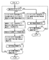
- the mounting flow of the electronic component by the mounting machine of Example 1 is shown (mounting flow until mounting of the first electronic component).
- the mounting flow of the electronic component by the mounting machine of Example 1 is shown (mounting flow after mounting the first electronic component).
- the other example of schematic structure of sequence data and reference mark data is shown.
- 2 shows a schematic configuration of a reading apparatus according to a second embodiment.
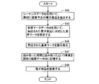
- the mounting flow of the electronic component by the mounting machine of Example 2 is shown (mounting flow until mounting of the first electronic component).
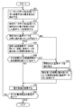
- the mounting flow of the electronic component by the mounting machine of Example 2 is shown (mounting flow after mounting the first electronic component).
- the reference mark reading method disclosed in this specification is a reading method executed in a mounting machine, and reads a plurality of reference marks marked on a circuit board.
- the fiducial mark reading method disclosed in the present specification includes a step of determining the timing for reading the fiducial mark for each fiducial mark. This determining step uses sequence data that defines the order in which components are mounted, reference mark data that defines reference marks to be referred to when mounting the components, and valid period data that defines the valid period of the standard marks. It is determined.
- the timing may mean an opportunity determined based on time, an opportunity determined based on the number of sequences, and / or an opportunity determined based on another index. For example, the timing may be an opportunity determined based on the time since the mounting machine started work.
- the timing may be an opportunity determined based on the number of times components are mounted on the circuit board.
- the effective period data is data describing an effective period in which the use of the reference mark position information is allowed, and is determined based on time, effective period determined based on the number of sequences, and / or others. It may be data describing an effective period determined based on the above criteria. For example, the effective period of the effective period data may be set based on an elapsed time after reading the reference mark. Alternatively, the effective period of the effective period data may be set based on the number of times components are mounted on the circuit board after reading the reference mark. The effective period of the effective period data may be a fixed value or a variable value depending on specific requirements.
- the effective period of the effective period data may be a function value that increases depending on the time after the mounting machine starts work.
- the fiducial mark reading method disclosed in the present specification further includes a step of selectively reading the fiducial mark that needs to be read at the timing determined in the determining step. As described above, the reading method disclosed in the present specification can read the necessary reference marks at a necessary timing, instead of reading all the reference marks at once.
- the step of determining may include a step of determining a plurality of reading timings including the first reading timing and the second reading timing using the valid period data.
- the determining step may further include a step of extracting a part to be mounted between the first reading timing and the second reading timing using the sequence data.
- the step of determining may further include a step of specifying a reference mark corresponding to the extracted part using the reference mark data. In this reading method, it is possible to avoid unnecessary reading of reference marks by reading only the reference marks necessary until the next reading timing at every reading timing.
- the reference mark reading method disclosed in the present specification may further include a step of storing, for each reference mark, a timing at which the reference mark is read in the reading step.
- the determining step may include a step of extracting a part to be mounted using sequence data.
- the step of determining may further include a step of specifying a reference mark corresponding to the part to be mounted using the reference mark data.
- the step of determining may further include a step of determining whether or not to read the reference mark by using the previously read timing and valid period data for each specified reference mark.
- the circuit board may be a multi-sided board including a plurality of circuit patterns.
- the plurality of reference marks may include local reference marks marked corresponding to each of the plurality of circuit patterns. Since a plurality of local reference marks are marked on the multi-sided substrate, the working time for reading these local reference marks tends to be longer. For this reason, by applying the reference mark reading method disclosed in this specification to the reading operation of such a multi-chip board, the work efficiency can be greatly improved.
- the integrated circuit on the circuit board is formed by being sequentially conveyed through a solder printer, a mounting machine, and a reflow furnace.
- the solder printer prints cream solder on the electronic component mounting position on the circuit board.
- the mounting machine mounts the electronic component at the mounting position on the circuit board on which the cream solder is printed.
- the reflow furnace solders an electronic component on a circuit board by performing heat treatment on the circuit board.
- the mounting machine 1 includes a plurality of modules 2 arranged adjacent to each other on a table 3.
- Each of the modules 2 has a common configuration, and includes a plurality of devices in a frame 4 that functions as a housing.
- FIG. 1 shows an example in which two modules 2 are adjacent to each other, and shows an exterior plate of one of the two modules 2 in a watermarked state.
- the module 2 includes a component supply device 10, a parts imaging device 20 having a parts camera, a nozzle stocker 30, a substrate transport device 40, a transfer device 50, and a mounting head 60.
- Each of the modules 2 includes an input / output device 6 on the surface of the exterior plate.
- the input / output device 6 is configured to be able to accept an operator input and to display status information of the module 2 and various instruction signals to the operator.
- the component supply device 10 is a device that supplies a plurality of types of electronic components to be mounted on the circuit board 5 to a component suction position, and includes a plurality of cassette-type feeders 11 arranged in parallel.
- the feeder main body 12 of the feeder 11 is configured to be detachable from the frame 4.
- the feeder 11 has a tape reel 13 around which a carrier tape on which electronic components are taped is wound. The carrier tape is fed out from the tape reel 13 by a predetermined pitch, and the electronic components are sequentially supplied to the component suction positions.
- the part imaging device 20 is fixed to the frame 4 and is disposed between the component supply device 10 and the substrate transfer device 40.
- the parts imaging device 20 has a parts camera composed of a CCD camera. After the electronic component is picked up at the component pick-up position of the feeder 11 and before being mounted on the circuit board 5 positioned on the board transfer device 40, the electronic component is stopped above the part image pickup device 20 and picked up by the parts camera.
- the mounter 1 recognizes the identification of the electronic component and the suction posture of the electronic component using the image data of the electronic component imaged by the parts imaging device 20. The suction posture of the electronic component is corrected by the rotation of the suction nozzle before the electronic component is mounted on the circuit board 5.
- the substrate transfer device 40 is fixed to the frame 4 and transfers the circuit board 5 along the transfer direction (X-axis direction) and positions the circuit board 5 at a predetermined work position.
- the substrate transfer device 40 is a double conveyor type in which a first transfer device 41 and a second transfer device 42 are arranged in two rows.
- the circuit board 5 transported by the substrate transport apparatus 40 is partitioned into a plurality of circuit blocks 5a, and a circuit pattern is formed in each circuit block 5a.
- the circuit board 5 is a multi-sided board that is divided into circuit blocks 5a after all electronic components are mounted.
- global reference marks M1 are marked at four corners.
- a local reference mark M2 is marked on each circuit block 5a. These global reference mark M1 and local reference mark M2 are used to align the work position of the circuit board 5 and the position of the electronic component mounting position.
- the transfer device 50 is fixed to the frame 4 and is an XY robot type.
- the transfer device 50 includes a Y-axis drive device 50Y and an X-axis drive device 50X.
- the Y-axis drive device 50Y has a drive mechanism that uses a linear motor, and is configured to be able to move the Y-axis slide member 53 in the Y-axis direction.
- the X-axis drive device 50X has a drive mechanism that uses a ball screw, and is configured to be able to move the X-axis slide member provided on the Y-axis slide member 53 in the X-axis direction.
- a mounting head 60 is fixed to the X-axis slide member.
- the mounting head 60 is attached with a mark camera including a suction nozzle and a CCD camera for sucking electronic components.
- the mark camera is used to image the reference marks M1 and M2 marked on the circuit board 5.
- the mounting head 60 is moved in the XY plane using the Y-axis driving device 50Y and the X-axis driving device 50X, and the component supply device 10, the parts imaging device 20, the nozzle stocker 30, and the substrate transport device.
- the upper part of 40 is comprised so that a movement is possible.
- the components of the Y-axis drive device 50Y and the X-axis drive device 50X generate heat due to the sliding friction of the guide mechanisms and the like of the Y-axis drive device 50Y and the X-axis drive device 50X.
- the components of the Y-axis drive device 50Y and the X-axis drive device 50X are thermally expanded, and the mounting accuracy of the electronic components is reduced.
- the position information of the reference marks M1 and M2 marked on the circuit board 5 is used to periodically align the work position of the circuit board 5 and the position of mounting the electronic component, The effect of such thermal expansion is compensated.
- the reading device 100 provided in the mounting machine 1 includes a control device 70 that controls the timing for reading the reference marks M ⁇ b> 1 and M ⁇ b> 2 marked on the circuit board 5.
- the control device 70 is connected to the storage device 80, the transfer device 50, the mark camera of the mounting head 60, and the input / output device 6.
- the storage device 80 is configured to be able to store sequence data 82, reference mark data 84, validity period data 86, and read timing data 88.
- FIG. 4 shows an example of the sequence data 82 and the reference mark data 84.
- the mounting order indicates a numeric string expressed in decimal.
- the mounting time indicates an elapsed time from the start of production by the mounting machine 1.
- the electronic component indicates the type of electronic component to be mounted on the circuit board 5.
- the reference mark indicates the type of the reference mark marked on the circuit board 5.
- the reference mark Ma is a local reference mark M2 marked on a specific circuit block 5a among the local reference marks M2 marked on the circuit board 5.
- the sequence data 82 defines the order of mounting the electronic components, and in this example, corresponds to data in which the mounting time is associated with the electronic components. For example, the sequence data 82 defines that the electronic component P1 is mounted at the mounting time T0, the electronic component P2 is mounted at the mounting time T0 + 1, and the electronic component P3 is mounted at the mounting time T0 + 2. Instead of this example, the sequence data 82 may be data in which the mounting order is associated with the electronic component. In this case, for example, the sequence data 82 defines that the electronic component P1 is mounted first, the electronic component P2 is mounted second, and the electronic component P3 is mounted third.
- the reference mark data 84 defines a reference mark that is referred to when the electronic component is mounted.
- the reference mark data 84 corresponds to data that associates the electronic component with the reference mark.
- the reference mark data 84 defines that the reference marks Ma and Mb are referred to when the electronic components P1 to Pn1 are mounted, and the reference marks Mc and Md are referred to when the electronic components Pn2 to Pm1 are mounted.
- the effective period data 86 defines an effective period in which the reference mark position information is allowed to be used. In this example, the effective period data 86 is time data such as “5 minutes”.
- the valid period of the reference mark may be determined empirically from the temperature rise curve during production by the mounting machine 1.
- the sequence data 82, the reference mark data 84, and the valid period data 86 can be input via the input / output device 6.
- the read timing data 88 is data that defines a plurality of read timings, and is created using the sequence data 82 and the valid period data 86. For example, when the effective period data 86 is “5 minutes”, a plurality of reading timings corresponding to the mounting time of the sequence data 82 are determined within a range in which the interval between successive reading timings does not exceed “5 minutes”. . As a result, read timing data 88 as shown in FIG. 5 is created. In this example, the read timing data 88 defines that the reference mark is read at the mounting times T0, T1, and T2.
- FIG. 6 shows a flow until the first electronic component to be mounted is mounted.
- the flow is until the electronic component P1 (see FIG. 4) is mounted.
- FIG. 7 shows a flow of mounting the electronic component after mounting the first electronic component.
- step S ⁇ b> 11 the control device 70 acquires sequence data 82 and valid period data 86.
- step S12 the control device 70 determines a plurality of reading timings and creates reading timing data 88 (see FIG. 5).
- step S ⁇ b> 13 the control device 70 uses the sequence data 82 to extract electronic components to be mounted between the first reading timing T ⁇ b> 0 and the next reading timing T ⁇ b> 1.
- step S ⁇ b> 14 the control device 70 uses the reference mark data 84 to specify a reference mark corresponding to the extracted electronic component. In this example, the reference marks Ma and Mb are specified.
- step S15 the control device 70 reads the specified reference marks Ma and Mb.
- the control device 70 uses the Y-axis drive circuit and the X-axis drive circuit so that the reference marks Ma and Mb are positioned within the imaging field of view of the mark camera attached to the mounting head 60.
- the apparatus 50 is driven and the reference marks Ma and Mb are imaged.
- the captured reference marks Ma and Mb are processed by the image processing unit and recognized.
- the mounting machine 1 is controlled so as to read only the reference marks Ma and Mb required by the next reading timing T1 among the plurality of reference marks marked on the circuit board 5.
- step S ⁇ b> 16 the electronic component P ⁇ b> 1 to be mounted first is mounted at the mounting position of the circuit board 5 using the position information of the reference marks Ma and Mb. Thereafter, mounting of electronic components is executed based on the flow of FIG.
- step S21 the control device 70 uses the read timing data 88 to determine whether or not it is a read timing. If it is within the work period between the first reading timing T0 and the next reading timing T1, the control device 70 determines that it is not the reading timing. Thereby, the mounting operation proceeds to step S23.
- step S23 the control device 70 uses the sequence data 82 to extract the next electronic component to be mounted.
- step S25 the extracted electronic component is mounted at the mounting position of the circuit board 5 using the position information of the reference marks Ma and Mb that has already been read.
- step S27 the control device 70 determines whether or not all the electronic components have been mounted. If it is determined that the mounting of all electronic components has been completed, the mounting operation is completed. If it is determined that the mounting of all the electronic components has not been completed, the mounting operation returns to step S21.
- step S21 the control device 70 determines that it is the reading timing. Thereby, the mounting operation proceeds to step S31.
- the control device 70 uses the sequence data 82 to extract electronic components that are to be mounted by the next reading timing T2.
- step S ⁇ b> 33 the control device 70 uses the reference mark data 84 to specify a reference mark corresponding to the extracted electronic component.
- the reference marks Mc and Md are specified.
- step S35 the control device 70 reads the specified reference marks Mc and Md.
- the mounting machine 1 is controlled so as to read only the reference marks Mc and Md required by the next reading timing T2 among the plurality of reference marks marked on the circuit board 5.
- step S ⁇ b> 36 the control device 70 uses the sequence data 82 to extract the next electronic component to be mounted.
- step S ⁇ b> 37 the extracted electronic component is mounted at the mounting position of the circuit board 5 using the position information of the read reference marks Mc and Md.
- step S39 the control device 70 determines whether or not all electronic components have been mounted. If it is determined that the mounting of all electronic components has been completed, the mounting operation is completed. If it is determined that the mounting of all the electronic components has not been completed, the mounting operation returns to step S21.
- the mounting machine 1 is configured not to read all the reference marks at a time at a plurality of reading timings, but to read only the reference marks necessary until the next reading timing. As a result, useless reading of reference marks can be avoided, and efficient reading work can be executed.
- the mode in which the type of the reference mark to be read is changed for each of a plurality of reading timings is illustrated for the sake of convenience.
- the technology disclosed in this specification It is not limited to such an aspect.
- the reference marks Ma and Mb necessary for the next mounting time T0 + A are read at the mounting time T0, and are necessary for the next mounting time T1 + B at the mounting time T0 + A.
- the reference marks Ma, Mb, Mc, and Md are read, and the quasi-marks Mc, Md, Me, and Mf that are required up to the next mounting time T2 + C are read at the mounting time T1 + B.
- the fixed time data mode in which the valid period described in the valid period data 86 is “5 minutes” is exemplified.
- the valid period described in the valid period data 86 may be time data represented by a function that increases depending on the time after the mounting machine 1 starts work.
- the effective period described in the effective period data 86 may be set based on the number of times electronic components are mounted on the circuit board 5.
- the reading device 101 provided in the mounting machine 1 according to the second embodiment includes reading history data 89 instead of the reading timing data 88 of the reading device 100 according to the first embodiment. It is characterized by.
- the reading history data 89 is configured to be able to store the timing at which the reference mark is read for each reference mark.
- the reading history data 89 is configured to be able to store the time for reading the reference mark for each reference mark.
- FIG. 10 shows a flow until the electronic component to be mounted first is mounted.
- the flow is until the electronic component P1 (see FIG. 4) is mounted.
- FIG. 11 shows a flow of mounting the electronic component after mounting the first electronic component.
- step S ⁇ b> 41 the control device 70 first extracts the electronic component P ⁇ b> 1 to be mounted using the sequence data 82.
- step S43 the control device 70 uses the reference mark data 84 to specify the reference marks Ma and Mb corresponding to the extracted electronic component P1.
- step S45 the control device 70 reads the specified reference marks Ma and Mb.
- step S47 the control device 70 stores in the reading history data 89 the time when the reference marks Ma and Mb are read and the fact that the reference marks Ma and Mb are read.
- step S49 using the position information of the reference marks Ma and Mb, the electronic component P1 to be mounted first is mounted at the mounting position of the circuit board. Thereafter, mounting of electronic components is executed based on the flow of FIG.
- step S51 the control device 70 uses the sequence data 82 to extract the next electronic component P2 to be mounted.
- step S52 the control device 70 uses the reference mark data 84 to specify the reference marks Ma and Mb corresponding to the extracted electronic component P2.
- step S53 the control device 70 uses the reading history data 89 to determine whether or not the specified reference marks Ma and Mb have been read before. If it is determined that it has been read, the mounting operation proceeds to step S54.
- step S54 the control device 70 uses the reading history data 89 to acquire the time when the reference marks Ma and Mb were read last time.
- step S55 the control device 70 determines whether or not the elapsed time from the previously read time exceeds the valid period (eg, “5 minutes”) defined by the valid period data 86. To do. If the elapsed time does not exceed the valid period, the control device 70 determines that the reference marks Ma and Mb are valid. Thereby, the mounting operation proceeds to step S56. In step S56, the extracted electronic component P2 is mounted at the mounting position of the circuit board using the position information of the reference marks Ma and Mb. Next, in step S57, the control device 70 determines whether or not all electronic components have been mounted. If it is determined that the mounting of all electronic components has been completed, the mounting operation is completed. If it is determined that the mounting of all the electronic components has not been completed, the mounting operation returns to step S51.
- the valid period eg, “5 minutes”
- step S55 the control device 70 determines in step S55 that the reference marks Ma and Mb are invalid. . Thereby, the mounting operation proceeds to step S58.
- step S58 the control device 70 reads the specified reference marks Ma and Mb.
- step S59 the control device 70 stores in the reading history data 89 the time when the reference marks Ma and Mb are read and the fact that the reference marks Ma and Mb are read. Accordingly, the latest time when the reference marks Ma and Mb are read is stored in the reading history data 89.
- step S53 the control device 70 determines in step S53 that the reference marks Mc and Md have not been read. Thereby, the mounting operation proceeds to step S58.
- step S58 the control device 70 reads the specified reference marks Mc and Md.
- step S ⁇ b> 59 the control device 70 stores the time when the reference marks Mc and Md are read and the fact that the reference marks Mc and Md are read in the reading history data 89.
- step S56 the extracted electronic component Pn2 is mounted at the mounting position of the circuit board using the position information of the reference marks Mc and Md.
- the mounting machine 1 is configured to determine whether the reference mark referred to when mounting the electronic component is valid or invalid each time the electronic component is mounted, and to read the reference mark only when the electronic component is invalid. ing. As a result, useless reading of reference marks can be avoided, and efficient reading work can be executed.
- step S53- Step S55 when the reference mark has been read before, the reference mark is compared with the effective period of the effective period data 86 every time an electronic component is mounted (step S53- Step S55) is exemplified.
- the reading history data 89 is periodically verified, and the fact that the reference mark whose elapsed time from the previous reading of the reference mark exceeds the effective period of the effective period data 86 is read. It may be invalidated in advance.
- the fixed time data mode in which the valid period described in the valid period data 86 is “5 minutes” is exemplified.
- time data represented by a function that increases depending on the time after the mounting machine 1 starts work may be used.
- the effective period described in the effective period data 86 may be set based on the number of times electronic components are mounted on the circuit board 5.
- Control device 80 Storage device 82: Sequence data 84: Reference mark data 86: Valid period data 88: Reading timing data
Landscapes
- Engineering & Computer Science (AREA)
- Operations Research (AREA)
- Manufacturing & Machinery (AREA)
- Microelectronics & Electronic Packaging (AREA)
- Supply And Installment Of Electrical Components (AREA)
- Length Measuring Devices By Optical Means (AREA)
Abstract
実装機において、回路基板に印されている複数の基準マークの読み取りを行う基準マークの読取方法は、部品を装着する順序を定めたシーケンスデータ、その部品を装着する際に参照する前記基準マークを定めた参照マークデータ、及び前記基準マークの有効期間を定めた有効期間データを用いて、前記基準マークを読み取るタイミングを前記基準マーク毎に決定するステップと、前記決定するステップで決定された前記タイミングにおいて、読み取りが必要とされた前記基準マークを選択的に読み取るステップと、を備える。
Description
本明細書で開示される技術は、回路基板に電子部品を実装する実装機(表面実装機又はチップマウンタともいう)に関する。本発明は特に、実装機において、回路基板に印されている複数の基準マークの読み取りを行う基準マークの読取方法に関する。
実装機は、電子部品を吸着した吸着ノズルを回路基板の装着位置に移動させ、回路基板に電子部品を装着する装置である。吸着ノズルは、回路基板の上方をXY平面内で移動可能な搭載ヘッドに取り付けられている。搭載ヘッドは、リニアモータ、ボールねじ等を利用した駆動機構を有する移載装置によって移動される。
特開平8-18289号公報で指摘されているように、このような移載装置の駆動機構では、搭載ヘッドを移動させるときに、ガイド機構等の摺動摩擦によって発熱する。このため、駆動機構の構成部品が熱膨張し、電子部品の装着精度が低下する。近年、電子部品の小型化により、1枚の回路基板に装着される電子部品の点数が増加し、1枚の回路基板の生産に要する時間が長くなっている。このため、一枚の回路基板の生産中における駆動機構の経時的な熱変位の影響により、装着精度の低下が問題となっている。
従来の実装機では、装着精度の低下を抑えるために、回路基板に印されている複数の基準マークを定期的に読み取り、電子部品の装着位置の補正を行なっている。しかしながら、従来の実装機では、全て基準マークを定期的に一括して読み取るように制御されていることから、作業効率の低下を招いている。本明細書では、複数の基準マークを効率的に読み取ることにより、作業効率の低下を抑えることが可能な基準マークの読取方法、及びそのような読取方法を実行する実装機を提供することを目的としている。
本明細書で開示される基準マークの読取方法は、実装機において実行される読取方法であり、回路基板に印されている複数の基準マークの読み取りを行う。基準マークの読取方法は、部品を搭載する順序を定めたシーケンスデータ、その部品を装着する際に参照する前記基準マークを定めた参照マークデータ、及び前記基準マークの有効期間を定めた有効期間データを用いて、前記基準マークを読み取るタイミングを前記基準マーク毎に決定するステップを備える。基準マークの読取方法はさらに、前記決定するステップで決定された前記タイミングにおいて、読み取りが必要とされた前記基準マークを選択的に読み取るステップを備える。
上記読取方法によれば、必要な基準マークを必要なタイミングで読み取ることができるので、作業効率の低下を抑えることができる。
本明細書で開示される実装機は、回路基板に印されている複数の基準マークの読み取りを行う読取装置を備えている。読取装置は、部品を装着する順序を定めたシーケンスデータ、その部品を装着する際に参照する前記基準マークを定めた参照マークデータ、及び前記基準マークの有効期間を定めた有効期間データを用いて、前記基準マークを読み取るタイミングを前記基準マーク毎に決定するステップを実行可能に構成されている。読取装置はさらに、前記決定するステップで決定された前記タイミングにおいて、読み取りが必要とされた前記基準マークを選択的に読み取るステップを実行可能に構成されている。
上記実装機によれば、必要な基準マークを必要なタイミングで読み取ることができるので、作業効率の低下を抑えることができる。
以下、本明細書で開示される技術の特徴を整理する。なお、以下に記す事項は、各々単独で技術的な有用性を有している。
本明細書で開示される基準マークの読取方法は、実装機において実行される読取方法であり、回路基板に印されている複数の基準マークの読み取りを行う。本明細書で開示される基準マークの読取方法は、基準マークを読み取るタイミングを基準マーク毎に決定するステップを備える。この決定するステップは、部品を装着する順序を定めたシーケンスデータ、その部品を装着する際に参照する基準マークを定めた参照マークデータ、及び基準マークの有効期間を定めた有効期間データを用いて決定される。ここで、タイミングとは、時間に基づいて定められる機会、シーケンス数に基づいて定められる機会、及び/又はその他の指標に基づいて定められる機会を意味してもよい。例えば、タイミングは、実装機が作業を開始してからの時間に基づいて定められた機会であってもよい。あるいは、タイミングは、回路基板に部品を装着した回数に基づいて定められた機会であってもよい。また、有効期間データは、基準マークの位置情報の使用が許容される有効期間を記述したデータであり、時間に基づいて定められる有効期間、シーケンス数に基づいて定められる有効期間、及び/又はその他の基準に基づいて定められる有効期間を記述したデータであってもよい。例えば、有効期間データの有効期間は、基準マークを読み取ってからの経過時間に基づいて設定されていてもよい。あるいは、有効期間データの有効期間は、基準マークを読み取ってから回路基板に部品を装着した回数に基づいて設定されていてもよい。また、この有効期間データの有効期間は、固定値であってもよく、特定の要件に依存する変数値であってもよい。例えば、有効期間データの有効期間は、実装機が作業を開始してからの時間に依存して増加する関数値であってもよい。本明細書で開示される基準マークの読取方法はさらに、決定するステップで決定されたタイミングにおいて、読み取りが必要とされた基準マークを選択的に読み取るステップを備える。このように、本明細書で開示される読取方法は、全ての基準マークを一括して読み取るのではなく、必要なタイミングで必要な基準マークを読み取ることができる。
決定するステップは、有効期間データを用いて、第1読取りタイミングと第2読取りタイミングを含む複数の読取りタイミングを決定するステップを有していてもよい。決定ステップはさらに、シーケンスデータを用いて、第1読取りタイミングと第2読取りタイミングの間に装着予定の部品を抽出するステップを有していてもよい。決定するステップはさらに、参照マークデータを用いて、抽出された部品に対応した基準マークを特定するステップを有していてもよい。この読取方法では、読取りタイミング毎に、次の読み取りタイミングまでに必要な基準マークのみを読み取ることにより、無駄な基準マークの読み取りを回避することができる。
本明細書で開示される基準マークの読取方法はさらに、読み取るステップで基準マークを読み取ったタイミングを基準マーク毎に記憶するステップをさらに備えていてもよい。この場合、決定するステップは、シーケンスデータを用いて、装着予定の部品を抽出するステップを有していてもよい。決定するステップはさらに、参照マークデータを用いて、装着予定の部品に対応した基準マークを特定するステップを有していてもよい。決定するステップはさらに、特定された基準マーク毎に、前回読み取ったタイミングと有効期間データを用いて、当該基準マークを読み取るか否かを決定するステップを有していてもよい。この読取方法では、部品を装着する毎に、その部品を装着する際に参照する基準マークが有効か無効かを判定し、無効な場合のみ基準マークを読取ることにより、無駄な基準マークの読み取りを回避することができる。
回路基板は、複数の回路パターンを含む多面取り基板であってもよい。この場合、複数の基準マークは、複数の回路パターンの各々に対応して印されているローカル基準マークを含んでいてもよい。多面取り基板には複数のローカル基準マークが印されているので、それらのローカル基準マークを読取る作業時間が長くなる傾向にある。このため、本明細書で開示される基準マークの読取り方法をこのような多面取り基板の読取り作業に適用することにより、作業効率を大幅に向上させることができる。
以下、図面を参照して、回路基板上に集積回路を形成する際に用いられる実装機を説明する。回路基板上の集積回路は、はんだ印刷機、実装機、及びリフロー炉を順に搬送されて形成される。はんだ印刷機は、回路基板上の電子部品の搭載位置にクリームはんだを印刷する。実装機は、クリームはんだが印刷された回路基板上の装着位置に電子部品を装着する。リフロー炉は、回路基板に熱処理を施すことで電子部品を回路基板上にハンダ付けする。
図1に示されるように、実装機1は、テーブル3上に隣接して配置されている複数のモジュール2を備えている。モジュール2の各々は、共通した構成となっており、筐体として機能するフレーム4内に複数の装置を備えている。図1は、2つのモジュール2が隣接した例を示しており、2つのモジュール2のうちの1つのモジュール2の外装板を透かした状態で示している。モジュール2は、部品供給装置10、パーツカメラを有するパーツ撮像装置20、ノズルストッカ30、基板搬送装置40、移載装置50、及び搭載ヘッド60を備える。また、モジュール2の各々は、外装板の表面に入出力装置6を備えている。この入出力装置6は、オペレータ入力を受け付け可能であるとともに、モジュール2のステータス情報及びオペレータへの各種指示信号を表示可能に構成されている。
部品供給装置10は、回路基板5に装着する複数種類の電子部品を部品吸着位置に供給する装置であり、複数のカセット式のフィーダ11が並設して構成されている。フィーダ11のフィーダ本体12は、フレーム4に着脱可能に構成されている。フィーダ11は、電子部品がテーピングされているキャリアテープが巻回されたテープリール13を有している。テープリール13からキャリアテープが所定ピッチずつ送り出され、電子部品が部品吸着位置に順次供給される。
パーツ撮像装置20は、フレーム4に固定されており、部品供給装置10と基板搬送装置40の間に配置されている。パーツ撮像装置20は、CCDカメラで構成されるパーツカメラを有する。電子部品は、フィーダ11の部品吸着位置で吸着された後、基板搬送装置40に位置決めされている回路基板5に装着される前に、パーツ撮像装置20の上方で停止され、パーツカメラで撮像される。実装機1は、パーツ撮像装置20で撮像した電子部品の画像データを利用して、電子部品の識別及び電子部品の吸着姿勢を認識する。電子部品の吸着姿勢は、電子部品が回路基板5に装着される前に吸着ノズルが自転することによって補正される。
基板搬送装置40は、フレーム4に固定されており、回路基板5を搬送方向(X軸方向)に沿って搬送するとともに、所定の作業位置で回路基板5を位置決めする。基板搬送装置40は、第1搬送装置41と第2搬送装置42を2列並設したダブルコンベアタイプである。
図2に示されるように、基板搬送装置40を搬送される回路基板5は、複数の回路ブロック5aに区画されており、各回路ブロック5aに回路パターンが形成されている。回路基板5は、全ての電子部品が装着された後に、回路ブロック5aごとに分割される多面取り基板である。回路基板5には、4つの角部にグローバル基準マークM1が印されている。回路ブロック5aの各々には、ローカル基準マークM2が印されている。これらグローバル基準マークM1及びローカル基準マークM2は、回路基板5の作業位置の位置合わせ及び電子部品の装着位置の位置合わせを行うために用いられる。
図1に戻る。移載装置50は、フレーム4に固定されており、XYロボットタイプである。移載装置50は、Y軸駆動装置50Y及びX軸駆動装置50Xを備えている。Y軸駆動装置50Yは、リニアモータを利用した駆動機構を有しており、Y軸スライド部材53をY軸方向に移動可能に構成されている。X軸駆動装置50Xは、ボールねじを利用した駆動機構を有しており、Y軸スライド部材53に設けられたX軸スライド部材をX軸方向に移動可能に構成されている。X軸スライド部材には、搭載ヘッド60が固定されている。搭載ヘッド60には、電子部品を吸着するための吸着ノズル及びCCDカメラで構成されるマークカメラが取り付けられている。マークカメラは、回路基板5に印されている基準マークM1,M2を撮像するために用いられる。
実装機1では、搭載ヘッド60がY軸駆動装置50Y及びX軸駆動装置50Xを用いてX-Y平面内で移動され、部品供給装置10、パーツ撮像装置20、ノズルストッカ30、及び基板搬送装置40の上方を移動可能に構成されている。搭載ヘッド60を移動させるときに、Y軸駆動装置50Y及びX軸駆動装置50Xのガイド機構等の摺動摩擦によってY軸駆動装置50Y及びX軸駆動装置50Xの構成部品が発熱する。このため、Y軸駆動装置50Y及びX軸駆動装置50Xの構成部品が熱膨張し、電子部品の装着精度が低下する。実装機1では、回路基板5に印されている基準マークM1,M2の位置情報を利用して、回路基板5の作業位置の位置合わせ及び電子部品の装着位置の位置合わせを定期的に行い、このような熱膨張の影響を補償する。
図3に示されるように、実装機1に設けられている読取装置100は、回路基板5に印されている基準マークM1,M2を読み取るタイミングを制御する制御装置70を備えている。制御装置70は、記憶装置80、移載装置50、搭載ヘッド60のマークカメラ、及び入出力装置6に接続されている。記憶装置80は、シーケンスデータ82、参照マークデータ84、有効期間データ86、及び読取りタイミングデータ88を記憶可能に構成されている。
図4に、シーケンスデータ82と参照マークデータ84の一例を示す。ここで、装着順序は、10進数で表された数字列を示している。装着時間は、実装機1による生産を開始してからの経過時間を示す。電子部品は、回路基板5に装着される電子部品の種類を示す。基準マークは、回路基板5に印されている基準マークの種類を示す。例えば、基準マークMaは、回路基板5に印されているローカル基準マークM2のうちの特定の回路ブロック5aに印されているローカル基準マークM2である。
シーケンスデータ82は、電子部品を搭載する順序を定めており、この例では、装着時間と電子部品を対応付けたデータに相当する。例えば、シーケンスデータ82は、装着時間T0で電子部品P1を装着し、装着時間T0+1で電子部品P2を装着し、装着時間T0+2で電子部品P3を装着することを定めている。なお、この例に代えて、シーケンスデータ82は、装着順序と電子部品を対応付けたデータであってもよい。この場合、例えば、シーケンスデータ82は、1番目に電子部品P1を装着し、2番目に電子部品P2を装着し、3番目に電子部品P3を装着することを定めている。参照マークデータ84は、電子部品を装着する際に参照する基準マークを定めており、この例では、電子部品と基準マークを対応付けたデータに相当する。例えば、参照マークデータ84は、電子部品P1~Pn1を装着するときは基準マークMa,Mbを参照し、電子部品Pn2~Pm1を装着するときは基準マークMc,Mdを参照することを定めている。有効期間データ86は、基準マークの位置情報を使用することが許容される有効期間を定めており、この例では、「5分」といった時間データである。基準マークの有効期間は、実装機1による生産時の温度上昇カーブから経験的に決定されてもよい。シーケンスデータ82、参照マークデータ84、及び有効期間データ86は、入出力装置6を介して入力することができる。
読取りタイミングデータ88は、複数の読取りタイミングを定めたデータであり、シーケンスデータ82と有効期間データ86を用いて作成される。例えば、有効期間データ86が「5分」である場合、連続する読取りタイミングの間隔が「5分」を越えない範囲内で、シーケンスデータ82の装着時間に対応した複数の読取りタイミングが決定される。これにより、図5に示されるような読取りタイミングデータ88が作成される。この例では、読取りタイミングデータ88は、装着時間T0,T1,T2において、基準マークの読み取りを行うことを定めている。
次に、図6及び図7を参照し、読取装置100を有する実装機1が電子部品を回路基板5に装着するフローを説明する。図6は、最初に装着予定の電子部品を装着するまでのフローを示す。この例では、電子部品P1(図4参照)を装着するまでのフローである。図7は、最初の電子部品を装着した以降の電子部品を装着するフローを示す。
図6に示されるように、まず、ステップS11において、制御装置70は、シーケンスデータ82と有効期間データ86を取得する。次に、ステップS12において、制御装置70は、複数の読取りタイミングを決定し、読取りタイミングデータ88を作成する(図5参照)。次に、ステップS13において、制御装置70は、シーケンスデータ82を用いて、最初の読取りタイミングT0と次の読取りタイミングT1の間に装着予定の電子部品を抽出する。次に、ステップS14において、制御装置70は、参照マークデータ84を用いて、抽出された電子部品に対応した基準マークを特定する。この例では、基準マークMa,Mbが特定される。次に、ステップS15において、制御装置70は、特定された基準マークMa,Mbを読み取る。具体的には、制御装置70は、搭載ヘッド60に取り付けられているマークカメラの撮像視野内に基準マークMa,Mbが位置するように、Y軸駆動回路及びX軸駆動回路を用いて移載装置50を駆動し、基準マークMa,Mbを撮像する。撮像された基準マークMa,Mbは、画像処理部で処理され、画像認識される。このように、実装機1では、回路基板5に印されている複数の基準マークのうち、次の読取りタイミングT1までに必要とされる基準マークMa,Mbのみを読み取るように制御される。次に、ステップS16において、基準マークMa,Mbの位置情報を利用して、最初に装着予定の電子部品P1を回路基板5の装着位置に装着する。これ以降は、図7のフローに基づいて電子部品の装着が実行される。
図7に示されるように、ステップS21において、制御装置70は、読取りタイミングデータ88を用いて、読取りタイミングか否かを判定する。最初の読取りタイミングT0と次の読取りタイミングT1の間の作業期間内であれば、制御装置70は、読取りタイミングでないと判定する。これにより、装着作業は、ステップS23に進む。ステップS23において、制御装置70は、シーケンスデータ82を用いて、次に装着予定の電子部品を抽出する。次に、ステップS25において、既に読み取られている基準マークMa,Mbの位置情報を利用して、抽出された電子部品が回路基板5の装着位置に装着される。次に、ステップS27において、制御装置70は、全ての電子部品の装着が終了したか否かを判定する。全ての電子部品の装着が終了していると判定されれば、装着作業が終了する。全ての電子部品の装着が終了していないと判定されれば、装着作業はステップS21に戻る。
電子部品の装着が進み、装着時間がT1に達すると、ステップS21において、制御装置70は、読取りタイミングであると判定する。これにより、装着作業は、ステップS31に進む。ステップS31において、制御装置70は、シーケンスデータ82を用いて、次の読取りタイミングT2までに装着予定の電子部品を抽出する。次に、ステップS33において、制御装置70は、参照マークデータ84を用いて、抽出された電子部品に対応した基準マークを特定する。この例では、基準マークMc,Mdが特定される。次に、ステップS35において、制御装置70は、特定された基準マークMc,Mdを読み取る。このように、実装機1では、回路基板5に印されている複数の基準マークのうち、次の読取りタイミングT2までに必要とされる基準マークMc,Mdのみを読み取るように制御される。次に、ステップS36において、制御装置70は、シーケンスデータ82を用いて、次に装着予定の電子部品を抽出する。次に、ステップS37において、読み取られた基準マークMc,Mdの位置情報を利用して、抽出された電子部品が回路基板5の装着位置に装着される。次に、ステップS39において、制御装置70は、全ての電子部品の装着が終了したか否かを判定する。全ての電子部品の装着が終了していると判定されれば、装着作業が終了する。全ての電子部品の装着が終了していないと判定されれば、装着作業はステップS21に戻る。
このように、実装機1は、複数の読取りタイミングにおいて全ての基準マークを一括して読み取るのではなく、次の読取りタイミングまでに必要な基準マークのみを読取るように構成されている。これにより、無駄な基準マークの読み取りを回避することができるので、効率的な読取り作業を実行することができる。
なお、上記例では、複数の読み取りタイミング毎に、読み取る基準マークの種類が変更される態様を例示したが、これは便宜の上で例示したものであり、本明細書で開示される技術はこのような態様に限定されるものではない。例えば、図8に示されるように、シーケンスデータ82と有効期間データ86を用いて決定される複数の読み取りタイミングが装着時間T0,T0+A,T1+B,T2+Cの場合、図6及び図7の装着フローに基づくと、装着時間T0において次の装着時間T0+Aまでに必要な基準マークMa,Mbが読み取られ、装着時間T0+Aにおいて次の装着時間T1+Bまでに必要な基準マークMa,Mb,Mc,Mdが読み取られ、装着時間T1+Bにおいて次の装着時間T2+Cまでに必要な準マークMc,Md,Me,Mfが読み取られる。
なお、実施例1の実装機1では、有効期間データ86に記述されている有効期間が「5分」という固定された時間データの態様を例示した。この例に代えて、有効期間データ86に記述されている有効期間は、実装機1が作業を開始してからの時間に依存して増加する関数で表される時間データであってもよい。また、有効期間データ86に記述されている有効期間が、回路基板5に電子部品を装着した回数に基づいて設定されていてもよい。
図9に示されるように、実施例2の実装機1に設けられている読取装置101は、実施例1の読取装置100の読取りタイミングデータ88に代えて、読取り履歴データ89を備えていることを特徴としている。読取り履歴データ89は、基準マークを読み取ったタイミングを基準マーク毎に記憶可能に構成されている。この例では、読取り履歴データ89は、基準マークを読取った時間を基準マーク毎に記憶可能に構成されている。
次に、図10及び図11を参照し、読取装置101を有する実装機1が電子部品を回路基板5に装着するフローを説明する。図10は、最初に装着予定の電子部品を装着するまでのフローを示す。この例では、電子部品P1(図4参照)を装着するまでのフローである。図11は、最初の電子部品を装着した以降の電子部品を装着するフローを示す。
図10に示されるように、まず、ステップS41において、制御装置70は、シーケンスデータ82を用いて、最初に装着予定の電子部品P1を抽出する。次に、ステップS43において、制御装置70は、参照マークデータ84を用いて、抽出された電子部品P1に対応した基準マークMa,Mbを特定する。次に、ステップS45において、制御装置70は、特定された基準マークMa,Mbを読み取る。次に、ステップS47において、制御装置70は、基準マークMa,Mbを読み取った時間と基準マークMa,Mbを読み取ったという事実を読取り履歴データ89に記憶する。次に、ステップS49において、基準マークMa,Mbの位置情報を利用して、最初に装着予定の電子部品P1が回路基板の装着位置に装着される。これ以降は、図11のフローに基づいて電子部品の装着が実行される。
図11に示されるように、ステップS51において、制御装置70は、シーケンスデータ82を用いて、次に装着予定の電子部品P2を抽出する。次に、ステップS52において、制御装置70は、参照マークデータ84を用いて、抽出された電子部品P2に対応した基準マークMa,Mbを特定する。次に、ステップS53において、制御装置70は、読取り履歴データ89を用いて、特定された基準マークMa,Mbを以前に読み取ったことがあるか否かを判定する。読取ったことがあると判定されれば、装着作業はステップS54に進む。ステップS54において、制御装置70は、読取り履歴データ89を用いて、前回、基準マークMa,Mbを読み取った時間を取得する。次に、ステップS55において、制御装置70は、その前回に読取った時間からの経過時間が有効期間データ86で定められている有効期間(例えば、「5分」)を越えている否かを判定する。経過時間が有効期間を越えていなければ、制御装置70は、基準マークMa,Mbが有効であると判定する。これにより、装着作業はステップS56に進む。ステップS56において、基準マークMa,Mbの位置情報を利用して、抽出された電子部品P2が回路基板の装着位置に装着される。次に、ステップS57において、制御装置70は、全ての電子部品の装着が終了したか否かを判定する。全ての電子部品の装着が終了していると判定されれば、装着作業が終了する。全ての電子部品の装着が終了していないと判定されれば、装着作業はステップS51に戻る。
このような装着作業が繰返され、基準マークMa,Mbを読み取った時間からの経過時間が有効期間を越えると、ステップS55において、制御装置70は、基準マークMa,Mbが無効であると判定する。これにより、装着作業はステップS58に進む。ステップS58において、制御装置70は、特定された基準マークMa,Mbを読み取る。次に、ステップS59において、制御装置70は、基準マークMa,Mbを読み取った時間と基準マークMa,Mbを読み取ったという事実を読取り履歴データ89に記憶する。これにより、基準マークMa,Mbを読取った最新の時間が読取り履歴データ89に記憶される。
また、このような装着作業が繰返され、電子部品Pn2を装着する段階になると、ステップS53において、制御装置70は、基準マークMc,Mdを読み取ったことがないと判定する。これにより、装着作業はステップS58に進む。ステップS58において、制御装置70は、特定された基準マークMc,Mdを読み取る。次に、ステップS59において、制御装置70は、基準マークMc,Mdを読み取った時間と基準マークMc,Mdを読み取ったという事実を読取り履歴データ89に記憶する。次に、ステップS56において、基準マークMc,Mdの位置情報を利用して、抽出された電子部品Pn2が回路基板の装着位置に装着される。
このように、実装機1は、電子部品を装着する毎に、その電子部品を装着する際に参照する基準マークが有効か無効かを判定し、無効な場合のみ基準マークを読取るように構成されている。これにより、無駄な基準マークの読み取りを回避することができるので、効率的な読取り作業を実行することができる。
なお、実施例2の実装機1では、以前に基準マークを読み取ったことがある場合、電子部品を装着する毎に、その基準マークを有効期間データ86の有効期間と比較する態様(ステップS53-ステップS55)を例示した。この例に代えて、読取り履歴データ89を定期的に検証し、前回に基準マークを読み取ってからの経過時間が有効期間データ86の有効期間を越えている基準マークに関しては、読み取ったという事実を予め無効にしてもよい。このようなステップを図11の装着フローと平行して実行することで、ステップS54とステップS55を省略することができるので、効率的な読取り作業を実行することができる。
なお、実施例2の実装機1では、有効期間データ86に記述されている有効期間が「5分」という固定された時間データの態様を例示した。この例に代えて、実装機1が作業を開始してからの時間に依存して増加する関数で表される時間データであってもよい。また、有効期間データ86に記述されている有効期間が、回路基板5に電子部品を装着した回数に基づいて設定されていてもよい。
以上、本技術の具体例を詳細に説明したが、これらは例示にすぎず、請求の範囲を限定するものではない。請求の範囲に記載の技術には、以上に例示した具体例を様々に変形、変更したものが含まれる。本明細書または図面に説明した技術要素は、単独であるいは各種の組み合わせによって技術的有用性を発揮するものであり、出願時の請求項に記載の組み合わせに限定されるものではない。また、本明細書または図面に例示した技術は複数目的を同時に達成するものであり、そのうちの一つの目的を達成すること自体で技術的有用性を持つものである。
70:制御装置
80:記憶装置
82:シーケンスデータ
84:参照マークデータ
86:有効期間データ
88:読取りタイミングデータ
80:記憶装置
82:シーケンスデータ
84:参照マークデータ
86:有効期間データ
88:読取りタイミングデータ
Claims (5)
- 実装機において、回路基板に印されている複数の基準マークの読み取りを行う基準マークの読取方法であって、
部品を装着する順序を定めたシーケンスデータ、その部品を装着する際に参照する前記基準マークを定めた参照マークデータ、及び前記基準マークの有効期間を定めた有効期間データを用いて、前記基準マークを読み取るタイミングを前記基準マーク毎に決定するステップと、
前記決定するステップで決定された前記タイミングにおいて、読み取りが必要とされた前記基準マークを選択的に読み取るステップと、を備える読取方法。 - 前記決定するステップは、
前記有効期間データを用いて、第1読取りタイミングと第2読取りタイミングを含む複数の読取りタイミングを決定するステップと、
前記シーケンスデータを用いて、前記第1読取りタイミングと前記第2読取りタイミングの間に装着予定の前記部品を抽出するステップと、
前記参照マークデータを用いて、抽出された前記部品に対応した前記基準マークを特定するステップと、を有する請求項1に記載の読取方法。 - 前記読み取るステップで前記基準マークを読み取ったタイミングを前記基準マーク毎に記憶するステップをさらに備えており、
前記決定するステップは、
前記シーケンスデータを用いて、装着予定の前記部品を抽出するステップと、
前記参照マークデータを用いて、前記装着予定の前記部品に対応した前記基準マークを特定するステップと、
特定された前記基準マーク毎に、前回読み取ったタイミングと前記有効期間データを用いて、当該基準マークを読み取るか否かを決定するステップと、を有する請求項1に記載の読取方法。 - 前記回路基板は、複数の回路パターンを含む多面取り基板であり、
前記複数の基準マークは、前記複数の回路パターンの各々に対応して印されているローカル基準マークを含んでいる請求項1~3のいずれか一項に記載の読取方法。 - 回路基板に印されている複数の基準マークの読み取りを行う読取装置を備えている実装機であって、
前記読取装置は、
部品を装着する順序を定めたシーケンスデータ、その部品を装着する際に参照する前記基準マークを定めた参照マークデータ、及び前記基準マークの有効期間を定めた有効期間データを用いて、前記基準マークを読み取るタイミングを前記基準マーク毎に決定するステップと、
前記決定するステップで決定された前記タイミングにおいて、読み取りが必要とされた前記基準マークを選択的に読み取るステップと、を実行可能に構成されている実装機。
Priority Applications (2)
| Application Number | Priority Date | Filing Date | Title |
|---|---|---|---|
| JP2014546792A JP6076999B2 (ja) | 2012-11-15 | 2012-11-15 | 実装機、及び基準マークの読取方法 |
| PCT/JP2012/079697 WO2014076804A1 (ja) | 2012-11-15 | 2012-11-15 | 実装機、及び基準マークの読取方法 |
Applications Claiming Priority (1)
| Application Number | Priority Date | Filing Date | Title |
|---|---|---|---|
| PCT/JP2012/079697 WO2014076804A1 (ja) | 2012-11-15 | 2012-11-15 | 実装機、及び基準マークの読取方法 |
Publications (1)
| Publication Number | Publication Date |
|---|---|
| WO2014076804A1 true WO2014076804A1 (ja) | 2014-05-22 |
Family
ID=50730744
Family Applications (1)
| Application Number | Title | Priority Date | Filing Date |
|---|---|---|---|
| PCT/JP2012/079697 Ceased WO2014076804A1 (ja) | 2012-11-15 | 2012-11-15 | 実装機、及び基準マークの読取方法 |
Country Status (2)
| Country | Link |
|---|---|
| JP (1) | JP6076999B2 (ja) |
| WO (1) | WO2014076804A1 (ja) |
Cited By (2)
| Publication number | Priority date | Publication date | Assignee | Title |
|---|---|---|---|---|
| JP2023161413A (ja) * | 2022-04-25 | 2023-11-07 | ヤマハ発動機株式会社 | 基板作業装置 |
| US12376276B2 (en) | 2019-05-28 | 2025-07-29 | Fuji Corporation | Fiducial mark allocation method, fiducial mark allocation device, mounting method and mounting system |
Citations (2)
| Publication number | Priority date | Publication date | Assignee | Title |
|---|---|---|---|---|
| JPH06126671A (ja) * | 1992-10-13 | 1994-05-10 | Matsushita Electric Ind Co Ltd | ロボット位置決め方法 |
| JP2007012914A (ja) * | 2005-06-30 | 2007-01-18 | Yamaha Motor Co Ltd | 部品実装方法および表面実装機 |
Family Cites Families (2)
| Publication number | Priority date | Publication date | Assignee | Title |
|---|---|---|---|---|
| JP2007214494A (ja) * | 2006-02-13 | 2007-08-23 | Yamaha Motor Co Ltd | マーク認識方法および表面実装機 |
| JP2009170516A (ja) * | 2008-01-11 | 2009-07-30 | Yamaha Motor Co Ltd | 表面実装機、及び電子部品実装方法 |
-
2012
- 2012-11-15 WO PCT/JP2012/079697 patent/WO2014076804A1/ja not_active Ceased
- 2012-11-15 JP JP2014546792A patent/JP6076999B2/ja active Active
Patent Citations (2)
| Publication number | Priority date | Publication date | Assignee | Title |
|---|---|---|---|---|
| JPH06126671A (ja) * | 1992-10-13 | 1994-05-10 | Matsushita Electric Ind Co Ltd | ロボット位置決め方法 |
| JP2007012914A (ja) * | 2005-06-30 | 2007-01-18 | Yamaha Motor Co Ltd | 部品実装方法および表面実装機 |
Cited By (3)
| Publication number | Priority date | Publication date | Assignee | Title |
|---|---|---|---|---|
| US12376276B2 (en) | 2019-05-28 | 2025-07-29 | Fuji Corporation | Fiducial mark allocation method, fiducial mark allocation device, mounting method and mounting system |
| JP2023161413A (ja) * | 2022-04-25 | 2023-11-07 | ヤマハ発動機株式会社 | 基板作業装置 |
| JP7849215B2 (ja) | 2022-04-25 | 2026-04-21 | ヤマハ発動機株式会社 | 基板作業装置 |
Also Published As
| Publication number | Publication date |
|---|---|
| JPWO2014076804A1 (ja) | 2016-09-08 |
| JP6076999B2 (ja) | 2017-02-08 |
Similar Documents
| Publication | Publication Date | Title |
|---|---|---|
| US10582651B2 (en) | Component mounting machine | |
| KR101051106B1 (ko) | 전자부품 실장장치 및 전자부품 실장방법 | |
| KR20180100363A (ko) | 전자 부품 핸들링 유닛 | |
| JP4828298B2 (ja) | 部品実装方法および部品実装装置 | |
| JP2009094283A (ja) | 実装基板の生産方法、表面実装機及び実装基板生産管理装置 | |
| JP6309962B2 (ja) | 組立機 | |
| JP2009170465A5 (ja) | ||
| JP4728423B2 (ja) | 電子部品の実装方法及び電子部品の実装機 | |
| JP2009170516A (ja) | 表面実装機、及び電子部品実装方法 | |
| JP6076999B2 (ja) | 実装機、及び基準マークの読取方法 | |
| JP6572437B2 (ja) | 部品実装装置および部品実装方法 | |
| JP5663151B2 (ja) | 部品実装方法および部品実装装置 | |
| JP4694516B2 (ja) | 部品実装方法および表面実装機 | |
| JP2003347794A (ja) | 電子回路部品取出し方法および取出し装置 | |
| JP5254875B2 (ja) | 実装機 | |
| JP4781945B2 (ja) | 基板処理方法および部品実装システム | |
| JP4651581B2 (ja) | 部品実装方法 | |
| CN108370662B (zh) | 安装头的移动误差检测装置及元件安装装置 | |
| JP6242478B2 (ja) | 部品装着装置 | |
| JP3564191B2 (ja) | 実装機の位置補正方法及びその装置 | |
| JP5768173B2 (ja) | 部品実装方法および部品実装装置 | |
| JP6086667B2 (ja) | 部品実装システム | |
| JP4954698B2 (ja) | 表面実装機および表面実装機の制御方法 | |
| JP5622886B2 (ja) | 部品実装方法 | |
| JP4339141B2 (ja) | 表面実装機 |
Legal Events
| Date | Code | Title | Description |
|---|---|---|---|
| 121 | Ep: the epo has been informed by wipo that ep was designated in this application |
Ref document number: 12888324 Country of ref document: EP Kind code of ref document: A1 |
|
| ENP | Entry into the national phase |
Ref document number: 2014546792 Country of ref document: JP Kind code of ref document: A |
|
| NENP | Non-entry into the national phase |
Ref country code: DE |
|
| 122 | Ep: pct application non-entry in european phase |
Ref document number: 12888324 Country of ref document: EP Kind code of ref document: A1 |