WO2014073405A1 - 光学表示パネルの連続製造方法および光学表示パネルの連続製造システム - Google Patents
光学表示パネルの連続製造方法および光学表示パネルの連続製造システム Download PDFInfo
- Publication number
- WO2014073405A1 WO2014073405A1 PCT/JP2013/079097 JP2013079097W WO2014073405A1 WO 2014073405 A1 WO2014073405 A1 WO 2014073405A1 JP 2013079097 W JP2013079097 W JP 2013079097W WO 2014073405 A1 WO2014073405 A1 WO 2014073405A1
- Authority
- WO
- WIPO (PCT)
- Prior art keywords
- optical
- optical film
- film
- cell
- display panel
- Prior art date
- Legal status (The legal status is an assumption and is not a legal conclusion. Google has not performed a legal analysis and makes no representation as to the accuracy of the status listed.)
- Ceased
Links
Images
Classifications
-
- G—PHYSICS
- G02—OPTICS
- G02F—OPTICAL DEVICES OR ARRANGEMENTS FOR THE CONTROL OF LIGHT BY MODIFICATION OF THE OPTICAL PROPERTIES OF THE MEDIA OF THE ELEMENTS INVOLVED THEREIN; NON-LINEAR OPTICS; FREQUENCY-CHANGING OF LIGHT; OPTICAL LOGIC ELEMENTS; OPTICAL ANALOGUE/DIGITAL CONVERTERS
- G02F1/00—Devices or arrangements for the control of the intensity, colour, phase, polarisation or direction of light arriving from an independent light source, e.g. switching, gating or modulating; Non-linear optics
- G02F1/01—Devices or arrangements for the control of the intensity, colour, phase, polarisation or direction of light arriving from an independent light source, e.g. switching, gating or modulating; Non-linear optics for the control of the intensity, phase, polarisation or colour
- G02F1/13—Devices or arrangements for the control of the intensity, colour, phase, polarisation or direction of light arriving from an independent light source, e.g. switching, gating or modulating; Non-linear optics for the control of the intensity, phase, polarisation or colour based on liquid crystals, e.g. single liquid crystal display cells
- G02F1/1303—Apparatus specially adapted to the manufacture of LCDs
-
- G—PHYSICS
- G02—OPTICS
- G02F—OPTICAL DEVICES OR ARRANGEMENTS FOR THE CONTROL OF LIGHT BY MODIFICATION OF THE OPTICAL PROPERTIES OF THE MEDIA OF THE ELEMENTS INVOLVED THEREIN; NON-LINEAR OPTICS; FREQUENCY-CHANGING OF LIGHT; OPTICAL LOGIC ELEMENTS; OPTICAL ANALOGUE/DIGITAL CONVERTERS
- G02F1/00—Devices or arrangements for the control of the intensity, colour, phase, polarisation or direction of light arriving from an independent light source, e.g. switching, gating or modulating; Non-linear optics
- G02F1/01—Devices or arrangements for the control of the intensity, colour, phase, polarisation or direction of light arriving from an independent light source, e.g. switching, gating or modulating; Non-linear optics for the control of the intensity, phase, polarisation or colour
- G02F1/13—Devices or arrangements for the control of the intensity, colour, phase, polarisation or direction of light arriving from an independent light source, e.g. switching, gating or modulating; Non-linear optics for the control of the intensity, phase, polarisation or colour based on liquid crystals, e.g. single liquid crystal display cells
- G02F1/133—Constructional arrangements; Operation of liquid crystal cells; Circuit arrangements
- G02F1/1333—Constructional arrangements; Manufacturing methods
- G02F1/1335—Structural association of cells with optical devices, e.g. polarisers or reflectors
- G02F1/133528—Polarisers
-
- G—PHYSICS
- G02—OPTICS
- G02B—OPTICAL ELEMENTS, SYSTEMS OR APPARATUS
- G02B5/00—Optical elements other than lenses
- G02B5/30—Polarising elements
- G02B5/3025—Polarisers, i.e. arrangements capable of producing a definite output polarisation state from an unpolarised input state
- G02B5/3033—Polarisers, i.e. arrangements capable of producing a definite output polarisation state from an unpolarised input state in the form of a thin sheet or foil, e.g. Polaroid
Definitions
- the present invention relates to an optical display panel continuous manufacturing method and an optical display panel continuous manufacturing system.
- the first polarizing film obtained by feeding out a strip-shaped first polarizing film having an absorption axis in the longitudinal direction from the first optical film roll and cutting the strip-shaped first polarizing film in the width direction is used as the liquid crystal cell.
- a continuous manufacturing method (so-called Roll to Panel (RTP) method) of a liquid crystal display panel in which a two-polarized film is bonded to a surface on the viewing side of the liquid crystal cell is disclosed (for example, see Patent Document 1). *
- the present invention has been made in view of the above problems, and an object of the present invention is to provide an optical display panel manufacturing method and a manufacturing system for manufacturing an optical display panel in which warpage is suppressed.
- the present invention is a method for continuously producing an optical display panel in which a first optical film is laminated on one side of an optical cell and a second optical film is laminated on the other side of the optical cell,
- the first optical film obtained by cutting the band-shaped first optical film in the width direction is supplied from the first optical film roll, and while transporting the optical cell, the first optical film is removed from the optical cell.
- the second optical film is taken out from and supplied from the housing portion in which the second optical film in a single wafer state is housed, and the second optical film is transported from the pair of sides facing the optical cell while transporting the optical cell.
- an optical film for example, a polarizing film
- an optical cell for example, a liquid crystal cell
- one surface is bonded by the RTP method and the other surface is an STP method.
- the sticking direction parallel (including the same).
- both the bonding direction and tension control can be secured, and the front and back of the optical cell (first and second surfaces) The tension can be easily canceled to make the stresses coincide (substantially coincide, substantially coincide), and the warpage of the optical display panel can be suppressed.
- the first bonding step and the second bonding step are performed on a series of conveyance units that convey the optical cell and the optical display panel.
- the thickness of the second optical film is larger than the thickness of the first polarizing film. That is, it is preferable to carry out an optical film having a larger thickness by a sheet to panel method (a method in which an optical film that has been in a single wafer state is bonded to an optical cell, hereinafter also referred to as an “STP method”).
- STP method since the optical film is bonded while adsorbing and releasing the optical film, the optical film is bonded without applying a large tension. It is not possible to apply a large tension to it).
- the RTP method is a continuous roll film, it is easy to apply tension, and conversely, if the film is bonded without applying tension (for example, free of tension), there is a problem of bubble generation and sticking displacement. Since it is likely to occur, bonding is performed while applying tension to the film. Therefore, a relatively thick (stress accumulation) optical film is bonded to one surface of the optical cell by the STP method, and a relatively thin (stress accumulation difficult) optical film is optically controlled by the RTP method while controlling the tension. By bonding to the other surface of the cell, warpage of the optical display panel can be further suppressed.
- the absorption axis of the first optical film bonded to one surface of the optical display panel and the absorption axis of the second optical film bonded to the other surface are orthogonal to each other,
- the absorption axis of the first optical film in a state wound around the first optical film roll is in the longitudinal direction
- the absorption axis of the strip-shaped second optical film used for manufacturing the single-wafer second optical film is in the longitudinal direction.
- This configuration makes it possible to manufacture a high-contrast optical display panel in which the occurrence of warpage is suppressed.
- the optical cell is a VA mode or IPS mode liquid crystal cell.
- the present invention is particularly suitable for producing a high-contrast VA mode or IPS mode liquid crystal display panel in which the occurrence of warpage is suppressed.
- Another aspect of the present invention is a system for continuously manufacturing an optical display panel in which a first optical film is laminated on one surface of an optical cell and a second optical film is laminated on the other surface of the optical cell.
- a series of transport units for transporting the optical cell and the optical display panel A first optical film supply unit for supplying the first optical film obtained by cutting the belt-shaped first optical film in the width direction from a first optical film roll; Supplying the first optical film from a pair of sides facing the optical cell while transporting the optical cell transported by the transport unit while feeding the first optical film supplied by the first optical film supply unit A first bonding portion to be bonded to one surface of the optical cell along the direction;
- a second optical film supply unit that takes out and supplies the second optical film from a storage unit in which the second optical film in a single wafer state is stored; While transporting the optical cell transported by the transport unit, the second optical film supplied by the second optical film supply unit is moved from the pair of sides facing the optical cell to the second optical film. And a second bonding part to be
- an optical film for example, a polarizing film
- an optical cell for example, a liquid crystal cell
- one surface is bonded by the RTP method and the other surface is an STP method.
- the sticking direction parallel (including the same).
- both the bonding direction and tension control can be secured, and the front and back of the optical cell (first and second surfaces) The tension can be easily canceled to make the stresses coincide (substantially coincide, substantially coincide), and the warpage of the optical display panel can be suppressed.
- either the process of a 1st bonding part and the process of a 2nd bonding part may be performed first, and the simultaneous or the bonding process period may partially overlap before and behind.
- the 1st pasting part and the 2nd pasting part are arranged in the conveyance part which conveys the optical cell and the optical display panel.
- the thickness of the second optical film is larger than the thickness of the first polarizing film.
- the absorption axis of the first optical film bonded to one surface of the optical display panel and the absorption axis of the second optical film bonded to the other surface are orthogonal to each other,
- the absorption axis of the first optical film in a state wound around the first optical film roll is in the longitudinal direction
- the absorption axis of the strip-shaped second optical film used for manufacturing the single-wafer second optical film is in the longitudinal direction.
- the optical cell is a VA mode or IPS mode liquid crystal cell.
- a method of supplying an optical film from an optical film roll for example, (1) a belt-like laminated optical film in which a belt-like optical film is laminated on a carrier film is fed out from the optical film roll.
- Examples of the method include a method of feeding a belt-shaped laminated optical film formed by laminating the formed belt-shaped optical film and supplying the optical film, and any of them can be used.
- the optical display panel continuous manufacturing system of this embodiment continuously manufactures an optical display panel in which a first optical film is laminated on one surface of an optical cell and a second optical film is laminated on the other surface of the optical cell.
- the first optical film obtained by cutting the belt-shaped first optical film in the width direction, and a series of transport units that transport the optical cell and the optical display panel.
- the first optical film supplied from the roll and the first optical film supplied by the first optical film supply unit are opposed to the optical cell while conveying the optical cell conveyed by the conveyance unit.
- a first bonding portion that is bonded to one surface of the optical cell along the supply direction of the first optical film from the side of the set and a second optical film in a single wafer state are accommodated.
- the second optical film supply unit that takes out and supplies the second optical film from the storage unit, and the second optical film supply unit that supplies the second optical film while conveying the optical cell conveyed by the conveyance unit.
- a second bonding portion that bonds the two optical films to the other surface of the optical cell along a supply direction of the second optical film from a pair of sides facing the optical cell.
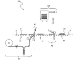
- FIGS. 1 to 3 are schematic views of a continuous manufacturing system for an optical display panel according to Embodiment 1.
- FIG. Hereinafter, a continuous manufacturing system of an optical display panel according to the present embodiment will be specifically described with reference to FIGS.
- a horizontally long liquid crystal cell is used as an optical cell
- a horizontally long liquid crystal display panel is used as an example of an optical display panel.
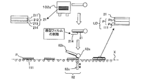
- the optical film roll those shown in FIGS. 1, 2, and 3 are used. That is, as the first optical film roll 1, a strip-shaped first polarizing film 11 (corresponding to the first optical film) having an absorption axis in the longitudinal direction is laminated on the first carrier film 12, and the liquid crystal cell P The belt-shaped first laminated optical film 10 having a width corresponding to the short side is wound.
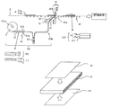
- the second optical film 21 in a single wafer state is manufactured using a strip-shaped second polarizing film having an absorption axis in the longitudinal direction and a strip-shaped linearly polarized light separating film having a reflection axis in the width direction.
- a conventionally known method such as a method described in JP-A-2004-250213 can be used.
- each of the second polarizing film and the linearly polarized light separating film is laminated in a single sheet state in advance, or one of the second polarizing film and the linearly polarized light separating film is preliminarily formed into a single sheet state, and the other is used as a strip film.
- stacking the film of a state is mentioned.
- belt-shaped 1st polarizing film 11 has a strip
- the second optical film 21 in a single wafer state is formed by laminating a linearly polarized light separating film 211, a second polarizing film 212, and an adhesive 213, and a release film 214 is temporarily attached to protect the adhesive 213.
- the continuous manufacturing system 100 for a liquid crystal display panel includes a series of transport units X that transport the liquid crystal cells P and the liquid crystal display panel LD, a first optical film supply unit 101, 1 bonding part 81, the 2nd optical film supply part 102, and the 2nd bonding part 82 are included.
- the transport unit X transports the liquid crystal cell P and the liquid crystal display panel LD.
- the conveyance unit X includes a plurality of conveyance rollers X1, a suction plate, and the like.
- the first optical film supply unit 101 is obtained by cutting the strip-shaped first polarizing film 11 having a width corresponding to the short side of the liquid crystal cell P in the width direction with a length corresponding to the long side of the liquid crystal cell P.
- the first polarizing film 111 is supplied from the first optical film roll 1 to the first bonding unit 81. Therefore, in this embodiment, the 1st optical film supply part 101 is the 1st delivery part 101a, the 1st cutting part 41, the 1st tension adjustment part 51, the 1st peeling part 61, the 1st winding part 71, and several Transport roller portion 101b.
- the first feeding unit 101 a has a feeding shaft on which the first optical film roll 1 is installed, and feeds the strip-shaped first laminated optical film 10 from the first optical film roll 1.
- the first feeding unit 101a may be provided with two feeding shafts. Thereby, it is possible to quickly join the roll 1 to the roll film installed on the other feeding shaft without replacing the roll 1 with a new roll.
- the first cutting part 41 is configured to have cutting means 41a and suction means 41b, and half-cuts the strip-shaped first laminated optical film 10 in the width direction with a length corresponding to the long side of the liquid crystal cell P (first).
- the band-shaped first polarizing film 11 is cut in the width direction without cutting the carrier film 12).
- the first cutting unit 41 uses the cutting unit 41a to fix the band-shaped first laminated optical film 10 from the first carrier film 12 side by using the suction unit 41b, and fixes the band-shaped first polarized light.
- the film 11 (the film body 11 a and the adhesive 11 b) is cut in the width direction, and the first polarizing film 111 having a size corresponding to the liquid crystal cell P is formed on the first carrier film 12.
- the cutting means 41a includes a cutter, a laser device, a combination thereof, and the like.
- the first tension adjusting unit 51 has a function of maintaining the tension of the belt-shaped first laminated optical film 10.
- the first tension adjusting unit 51 is configured to include a dancer roll, but is not limited thereto.
- the first peeling unit 61 peels the first polarizing film 111 from the first carrier film 12 by folding the first laminated optical film 10 having the first carrier film 12 on the inside.
- Examples of the first peeling portion 61 include a wedge-shaped member and a roller.
- the first winding unit 71 winds up the first carrier film 12 from which the first polarizing film 111 has been peeled off.
- the first winding unit 71 has a winding shaft on which a roll for winding the first carrier film 12 is installed.
- the 1st bonding part 81 was supplied by the 1st optical film supply part 101, conveying the liquid crystal cell P conveyed by the conveyance part X, making the long side direction parallel to a conveyance direction (1st peeling part).
- a surface Pa on the viewing surface side of the liquid crystal cell P from the short side of the liquid crystal cell P along the supply direction of the first polarizing film 111 (long side direction of the liquid crystal cell P). Are bonded together via an adhesive 11b.
- the first bonding unit 81 includes a pair of bonding rollers 81a and 81b, and at least one of the bonding rollers 81a and 81b includes a driving roller.
- the 2nd optical film supply part 102 takes out the 2nd optical film 21 of a sheet
- the 2nd bonding part 82 is the 2nd optical film 21 supplied by the 2nd optical film supply part 102, conveying the liquid crystal cell P conveyed by the conveyance part X with the long side direction parallel to a conveyance direction. Is bonded to the surface Pb on the back side of the liquid crystal cell P from the short side of the liquid crystal cell P.
- the second bonding unit 82 includes a moving unit (not shown) that moves the sheet-shaped second optical film 21 from the housing unit 102c to the bonding position, and a sheet-fed release film 214 that has a sheet-fed state. 2
- the liquid crystal cell P is conveyed in contact with the surface of the liquid crystal cell P, a peeling portion (not shown) that peels from the optical film 21, a suction portion 82b that adsorbs the second optical film 21 in a single wafer state, a bonding roller 82a Drive roller 82c.
- the storage portion 102c is not limited to the form described in FIGS. 1 and 3 and may have other shapes, for example, a container having a mounting table for mounting the second optical film 21 in a single wafer state.
- the pedestal may be covered around it.
- the moving unit moves to the second optical film 21 in a single-wafer state placed in the accommodating unit 102c, and adsorbs the surface of the second optical film 21 at the adsorbing unit 82b and moves to the bonding position.
- the peeling portion peels the single-wafer release film 214 from the single-wafer second optical film 21.
- the peeling unit may peel the release film 214 by bonding the adhesive tape to the surface of the release film 214 using, for example, an adhesive tape and moving the adhesive tape.
- the second optical film 21 in a single wafer state adsorbed by the adsorbing part 82b is sent to the laminating roller 82a at the tip position, and the laminating roller 82a is rotated to be on the surface Pb on the back side of the liquid crystal cell P.
- the second optical film 21 is bonded from the short side.
- the driving roller 82c and the bonding roller 82a sandwich the liquid crystal cell P and the second optical film 21 and convey them downstream.
- the driving roller 82c and the bonding roller 82a may be driven together, or the driving roller 82c may be driven.
- the first optical film supply unit and the second optical film supply unit are arranged in the transport unit X of the liquid crystal cell so that the supply directions of the first polarizing film and the second optical film are parallel to each other. Therefore, the space occupied by the apparatus can be reduced. Moreover, in this embodiment, the bonding direction of the 1st polarizing film 111 in the 1st bonding part 81 with respect to liquid crystal cell P and the bonding direction of the 2nd optical film 21 in the 2nd bonding part 82 are parallel. Therefore, the warp of the liquid crystal display panel can be suitably suppressed.
- the first bonding unit bonds the first polarizing film from the lower side of the liquid crystal cell
- the second bonding unit bonds the second optical film from the upper side of the liquid crystal cell. It is not limited to.
- the first bonding unit may bond the first polarizing film from the upper side of the liquid crystal cell
- the second bonding unit may bond the second optical film from the lower side of the liquid crystal cell.
- the first polarizing film 111 is bonded to the surface Pa on the viewing side of the liquid crystal cell P along the supply direction of the first polarizing film 111 from the short side of the liquid crystal cell P, and the second optical film 21. Is bonded to the surface Pb on the back side of the liquid crystal cell P along the supply direction of the second optical film from the short side of the liquid crystal cell P. As long as it is bonded so that the absorption axis is orthogonal (crossed Nicols), it is not limited to this.
- the first polarizing film 111 may be bonded from the long side of the liquid crystal cell P, and the second optical film 21 may be bonded from the long side of the liquid crystal cell P.
- the width and cutting size of the second optical film are set according to whether the second optical film is bonded from the long side or the short side of the liquid crystal cell. Moreover, it bonds together so that the absorption axis of each polarizing film of the visual recognition side and back side of a liquid crystal cell may orthogonally cross (cross Nicol).
- the continuous manufacturing method of the optical display panel of Embodiment 1 continuously manufactures an optical display panel in which a first optical film is laminated on one surface of an optical cell and a second optical film is laminated on the other surface of the optical cell.
- the first optical film obtained by cutting the strip-shaped first optical film in the width direction is supplied from a first optical film roll, and the first optical film is conveyed while transporting the optical cell.
- the second optical film is taken out and supplied from the accommodated accommodating part, and the first optical film is conveyed along the supply direction of the second optical film from a pair of sides facing the optical cell while conveying the optical cell.
- the absorption axis of the first optical film bonded to one surface of the optical display panel and the absorption axis of the second optical film bonded to the other surface are orthogonal to each other and wound around the first optical film roll.
- the absorption axis of the first optical film in the formed state is in the longitudinal direction
- the absorption axis of the band-shaped second optical film used for manufacturing the second optical film in the sheet state is in the longitudinal direction.
- the second optical film is a laminated optical film in which a polarizing film and a linearly polarized light separating film are laminated, but is not limited thereto.
- the second optical film include a broadband retardation film and a laminated optical film in which a broadband retardation film and a polarizing film are laminated.
- the broadband retardation film is exemplified by a film in which a ⁇ / 4 retardation film and a ⁇ / 2 retardation film are laminated.
- Embodiment 1 As the optical film roll, a roll-shaped laminated optical film obtained by laminating a band-shaped optical film on a carrier film is used, but the configuration of the optical film roll is not limited to this. For example, by appropriately using a belt-shaped laminated optical film formed by laminating a band-shaped optical film in which a plurality of score lines are formed in the width direction on a carrier film (a cut optical film roll). Also good. In addition, a cutting part becomes unnecessary in the optical film supply part which supplies an optical film from the optical film roll with a notch.
- the cutting unit cuts the band-shaped optical film in the width direction and forms the optical film having a size corresponding to the optical cell on the carrier film.
- the band-shaped optical film is formed.
- the band-shaped optical film is cut in the width direction (skip cut) so as to avoid the defective part of the optical film of the optical film of the size corresponding to the optical cell on the carrier film (the non-defective optical that is bonded to the optical cell)
- an optical film including a defect portion may be formed in a size smaller than the optical cell (more preferably in a size as small as possible).
- each optical film roll a band-shaped optical film formed in the width direction so that a plurality of score lines avoid a defective portion is laminated on the carrier film, and corresponds to an optical cell on the carrier film.
- an optical film including a defective portion is formed in a size smaller than the optical cell (more preferably in a size as small as possible).
- the yield can be effectively improved by using a roll-shaped laminated optical film (an optical film roll having a cut).
- the optical film including the defective portion is peeled off from the carrier film and discharged, or wound around the winding portion together with the carrier film so as not to be bonded to the optical cell.
- a horizontally-long rectangular optical cell and an optical display panel have been described as examples.
- the shape of the optical cell and the optical display panel includes a pair of opposing sides and another pair of opposing sides. As long as it is a shape, it is not particularly limited.
- the film body of the polarizing film is, for example, a polarizer (thickness is generally about 1 to 80 ⁇ m) and a polarizer protective film (thickness is generally about 1 to 500 ⁇ m) attached to one or both sides of the polarizer. Formed without an agent or adhesive.
- a polarizer usually has an absorption axis in the stretching direction.
- a polarizing film including a long polarizer having an absorption axis in the longitudinal direction is also referred to as “MD polarizing film”, and a polarizing film including a long polarizer having an absorption axis in the width direction is also referred to as “TD polarizing film”. .
- films constituting the film body include, for example, retardation films such as ⁇ / 4 plates and ⁇ / 2 plates (thickness is generally 10 to 200 ⁇ m), viewing angle compensation films, brightness enhancement films, surface protection films, etc. Is mentioned.
- the thickness of the laminated optical film is, for example, in the range of 10 ⁇ m to 500 ⁇ m.
- the polarizer is obtained, for example, by dyeing, crosslinking, stretching, and drying a polyvinyl alcohol film.
- Each treatment of dyeing, crosslinking and stretching of the polyvinyl alcohol film need not be performed separately and may be performed simultaneously, and the order of the treatments may be arbitrary.
- a polyvinyl alcohol film is immersed in a solution containing iodine or a dichroic dye, dyed by adsorbing iodine or a dichroic dye, and stretched 3 times in a solution containing boric acid or borax. After uniaxial stretching at ⁇ 7 times, it is washed and dried.
- the pressure-sensitive adhesive is not particularly limited, and examples thereof include an acrylic pressure-sensitive adhesive, a silicone pressure-sensitive adhesive, and a urethane pressure-sensitive adhesive.
- the layer thickness of the pressure-sensitive adhesive is preferably in the range of 10 ⁇ m to 50 ⁇ m, for example.
- Examples of the peeling force between the pressure-sensitive adhesive and the carrier film include 0.15 (N / 50 mm width sample), but are not particularly limited thereto. The peeling force is measured according to JIS Z0237.
- carrier film for example, a conventionally known film such as a plastic film (for example, a polyethylene terephthalate film, a polyolefin film, or the like) can be used.
- a plastic film for example, a polyethylene terephthalate film, a polyolefin film, or the like
- an appropriate material according to the prior art such as a silicone-based, long-chain alkyl-based, fluorine-based or molybdenum sulfide-coated material may be used.
- the carrier film is generally called a release film (separator film).
- the release film 214 of Embodiment 1 the same film as the carrier film can be used.
- Examples of the film body of the linearly polarized light separation film include a reflective polarizing film having a multilayer structure having a reflection axis and a transmission axis.
- the reflective polarizing film can be obtained, for example, by alternately laminating and stretching a plurality of polymer films A and B of two different materials.
- the refractive index of only material A increases and changes in the stretching direction, birefringence is developed, and the stretching direction having a difference in refractive index at the interface of material AB becomes the reflection axis, and the direction in which no refractive index difference occurs (non-stretching direction). It becomes the transmission axis.
- This reflective polarizing film has a transmission axis in its longitudinal direction and a reflection axis in its short direction (width direction).
- a commercially available product may be used as it is, or a commercially available product may be used after secondary processing (for example, stretching).
- 3M company brand name DBEF and 3M company brand name APF are mentioned, for example.
- the liquid crystal cell has a structure in which a liquid crystal layer is sealed between a pair of substrates (a first substrate (viewing side surface) Pa and a second substrate (back surface) Pb) disposed to face each other.
- a liquid crystal layer is sealed between a pair of substrates (a first substrate (viewing side surface) Pa and a second substrate (back surface) Pb) disposed to face each other.
- VA vertical alignment
- IPS in-plane switching
- a liquid crystal display panel has a polarizing film bonded to one or both sides of a liquid crystal cell, and a drive circuit is incorporated as necessary.
- Organic EL cell (Organic EL cell, organic EL display panel)
- the organic EL cell has a configuration in which an electroluminescent layer is sandwiched between a pair of electrodes.
- an arbitrary type such as a top emission method, a bottom emission method, a double emission method, or the like can be used.
- the organic EL display panel has a polarizing film bonded to one or both sides of an organic EL cell, and a drive circuit is incorporated as necessary.
Landscapes
- Physics & Mathematics (AREA)
- Nonlinear Science (AREA)
- General Physics & Mathematics (AREA)
- Optics & Photonics (AREA)
- Chemical & Material Sciences (AREA)
- Crystallography & Structural Chemistry (AREA)
- Mathematical Physics (AREA)
- Engineering & Computer Science (AREA)
- Manufacturing & Machinery (AREA)
- Liquid Crystal (AREA)
- Polarising Elements (AREA)
- Devices For Indicating Variable Information By Combining Individual Elements (AREA)
Priority Applications (2)
| Application Number | Priority Date | Filing Date | Title |
|---|---|---|---|
| CN201380054082.1A CN104737065B (zh) | 2012-11-09 | 2013-10-28 | 光学显示面板的连续制造方法及光学显示面板的连续制造系统 |
| KR1020157015007A KR101646479B1 (ko) | 2012-11-09 | 2013-10-28 | 광학 표시 패널의 연속 제조 방법 및 광학 표시 패널의 연속 제조 시스템 |
Applications Claiming Priority (2)
| Application Number | Priority Date | Filing Date | Title |
|---|---|---|---|
| JP2012-247682 | 2012-11-09 | ||
| JP2012247682A JP5782010B2 (ja) | 2012-11-09 | 2012-11-09 | 光学表示パネルの連続製造方法および光学表示パネルの連続製造システム |
Publications (1)
| Publication Number | Publication Date |
|---|---|
| WO2014073405A1 true WO2014073405A1 (ja) | 2014-05-15 |
Family
ID=50684514
Family Applications (1)
| Application Number | Title | Priority Date | Filing Date |
|---|---|---|---|
| PCT/JP2013/079097 Ceased WO2014073405A1 (ja) | 2012-11-09 | 2013-10-28 | 光学表示パネルの連続製造方法および光学表示パネルの連続製造システム |
Country Status (5)
| Country | Link |
|---|---|
| JP (1) | JP5782010B2 (enExample) |
| KR (1) | KR101646479B1 (enExample) |
| CN (1) | CN104737065B (enExample) |
| TW (1) | TWI524985B (enExample) |
| WO (1) | WO2014073405A1 (enExample) |
Families Citing this family (12)
| Publication number | Priority date | Publication date | Assignee | Title |
|---|---|---|---|---|
| JP6095711B2 (ja) * | 2015-02-19 | 2017-03-15 | 住友化学株式会社 | 積層光学フィルムの製造方法 |
| KR101674354B1 (ko) * | 2016-05-30 | 2016-11-22 | 주식회사 엘지화학 | 광학 표시 소자의 제조 시스템 및 제조 방법 |
| KR101674352B1 (ko) | 2016-05-30 | 2016-11-08 | 주식회사 엘지화학 | 광학 표시 소자의 제조 시스템 및 제조 방법 |
| JP6732580B2 (ja) * | 2016-07-22 | 2020-07-29 | 日東電工株式会社 | 光学表示パネルの製造方法と光学表示パネルの製造システム |
| JP6792367B2 (ja) * | 2016-07-22 | 2020-11-25 | 日東電工株式会社 | 枚葉状の光学フィルム |
| JP6792366B2 (ja) * | 2016-07-22 | 2020-11-25 | 日東電工株式会社 | 光学フィルムセット及びその製造方法 |
| JP6654113B2 (ja) * | 2016-07-22 | 2020-02-26 | 日東電工株式会社 | 光学表示パネルの製造方法と光学表示パネルの製造システム |
| KR102042053B1 (ko) | 2016-08-25 | 2019-11-07 | 주식회사 엘지화학 | 디스플레이 유닛의 제조 시스템 |
| JP6651638B2 (ja) | 2016-09-06 | 2020-02-19 | 沢井製薬株式会社 | 口腔内崩壊錠添加用組成物 |
| JP6538014B2 (ja) * | 2016-09-06 | 2019-07-03 | 日東電工株式会社 | 光学的表示ユニットの連続製造装置及び連続製造方法 |
| JP6505877B1 (ja) * | 2018-01-04 | 2019-04-24 | 日東電工株式会社 | 切目を有する長尺の光学フィルムを搬送する搬送装置、並びに、光学表示パネルの連続製造システム |
| JP7389703B2 (ja) * | 2019-12-25 | 2023-11-30 | 住友化学株式会社 | 積層体の製造方法、及び、貼合装置 |
Citations (3)
| Publication number | Priority date | Publication date | Assignee | Title |
|---|---|---|---|---|
| JP2010256757A (ja) * | 2009-04-28 | 2010-11-11 | Sumitomo Chemical Co Ltd | 光学表示パネルの製造方法 |
| JP2011197651A (ja) * | 2010-02-24 | 2011-10-06 | Sumitomo Chemical Co Ltd | 液晶表示装置の製造方法 |
| JP2012103594A (ja) * | 2010-11-12 | 2012-05-31 | Nitto Denko Corp | 液晶表示装置の製造方法 |
Family Cites Families (7)
| Publication number | Priority date | Publication date | Assignee | Title |
|---|---|---|---|---|
| JP2823970B2 (ja) | 1991-04-05 | 1998-11-11 | 浜松ホトニクス株式会社 | 近接場走査光学顕微鏡 |
| KR101010990B1 (ko) | 2006-10-17 | 2011-01-26 | 닛토덴코 가부시키가이샤 | 광학 부재 부착방법 및 그것을 이용한 장치 |
| JP5313002B2 (ja) | 2008-04-07 | 2013-10-09 | 日東電工株式会社 | 光学表示装置の製造方法 |
| JP4669070B2 (ja) * | 2009-05-21 | 2011-04-13 | 日東電工株式会社 | 光学表示装置の製造システム及び製造方法 |
| JP2012032559A (ja) | 2010-07-30 | 2012-02-16 | Sumitomo Chemical Co Ltd | ロール状偏光板のセット及びその製造方法並びに液晶パネルの製造方法 |
| JP2012053077A (ja) | 2010-08-31 | 2012-03-15 | Sumitomo Chemical Co Ltd | ロール状偏光板のセット及びその製造方法並びに液晶パネルの製造方法 |
| JP4921597B1 (ja) * | 2011-03-18 | 2012-04-25 | 日東電工株式会社 | 液晶表示パネルの連続製造システムおよび液晶表示パネルの連続製造方法、並びに、検査装置および検査方法 |
-
2012
- 2012-11-09 JP JP2012247682A patent/JP5782010B2/ja active Active
-
2013
- 2013-10-28 KR KR1020157015007A patent/KR101646479B1/ko active Active
- 2013-10-28 WO PCT/JP2013/079097 patent/WO2014073405A1/ja not_active Ceased
- 2013-10-28 CN CN201380054082.1A patent/CN104737065B/zh active Active
- 2013-11-08 TW TW102140736A patent/TWI524985B/zh active
Patent Citations (3)
| Publication number | Priority date | Publication date | Assignee | Title |
|---|---|---|---|---|
| JP2010256757A (ja) * | 2009-04-28 | 2010-11-11 | Sumitomo Chemical Co Ltd | 光学表示パネルの製造方法 |
| JP2011197651A (ja) * | 2010-02-24 | 2011-10-06 | Sumitomo Chemical Co Ltd | 液晶表示装置の製造方法 |
| JP2012103594A (ja) * | 2010-11-12 | 2012-05-31 | Nitto Denko Corp | 液晶表示装置の製造方法 |
Also Published As
| Publication number | Publication date |
|---|---|
| KR101646479B1 (ko) | 2016-08-05 |
| JP5782010B2 (ja) | 2015-09-24 |
| TW201422415A (zh) | 2014-06-16 |
| CN104737065A (zh) | 2015-06-24 |
| KR20150082542A (ko) | 2015-07-15 |
| JP2014095833A (ja) | 2014-05-22 |
| CN104737065B (zh) | 2016-09-07 |
| TWI524985B (zh) | 2016-03-11 |
Similar Documents
| Publication | Publication Date | Title |
|---|---|---|
| JP5782010B2 (ja) | 光学表示パネルの連続製造方法および光学表示パネルの連続製造システム | |
| JP5744819B2 (ja) | 光学表示パネルの連続製造方法および光学表示パネルの連続製造システム | |
| JP5945143B2 (ja) | 光学フィルムロールセットおよび光学フィルムロールセットの製造方法。 | |
| TWI551918B (zh) | A manufacturing method of a liquid crystal display element, and a manufacturing system of a liquid crystal display device | |
| JP5905761B2 (ja) | 光学表示パネルの連続製造方法および光学表示パネルの連続製造システム | |
| JP6082140B2 (ja) | 光学表示パネルの連続製造方法および光学表示パネルの連続製造システム | |
| JP5933066B2 (ja) | 光学表示パネルの連続製造方法および光学表示パネルの連続製造システム | |
| JP6148755B2 (ja) | 光学表示パネルの連続製造方法および光学表示パネルの連続製造システム |
Legal Events
| Date | Code | Title | Description |
|---|---|---|---|
| 121 | Ep: the epo has been informed by wipo that ep was designated in this application |
Ref document number: 13852632 Country of ref document: EP Kind code of ref document: A1 |
|
| NENP | Non-entry into the national phase |
Ref country code: DE |
|
| ENP | Entry into the national phase |
Ref document number: 20157015007 Country of ref document: KR Kind code of ref document: A |
|
| 122 | Ep: pct application non-entry in european phase |
Ref document number: 13852632 Country of ref document: EP Kind code of ref document: A1 |