WO2014069217A1 - 偏光素子、偏光素子の製造方法、液晶表示装置、及び、液晶表示装置の製造方法 - Google Patents
偏光素子、偏光素子の製造方法、液晶表示装置、及び、液晶表示装置の製造方法 Download PDFInfo
- Publication number
- WO2014069217A1 WO2014069217A1 PCT/JP2013/077731 JP2013077731W WO2014069217A1 WO 2014069217 A1 WO2014069217 A1 WO 2014069217A1 JP 2013077731 W JP2013077731 W JP 2013077731W WO 2014069217 A1 WO2014069217 A1 WO 2014069217A1
- Authority
- WO
- WIPO (PCT)
- Prior art keywords
- polarizing element
- electrode
- transport layer
- organic semiconductor
- semiconductor layer
- Prior art date
- Legal status (The legal status is an assumption and is not a legal conclusion. Google has not performed a legal analysis and makes no representation as to the accuracy of the status listed.)
- Ceased
Links
Images





























Classifications
-
- G—PHYSICS
- G02—OPTICS
- G02F—OPTICAL DEVICES OR ARRANGEMENTS FOR THE CONTROL OF LIGHT BY MODIFICATION OF THE OPTICAL PROPERTIES OF THE MEDIA OF THE ELEMENTS INVOLVED THEREIN; NON-LINEAR OPTICS; FREQUENCY-CHANGING OF LIGHT; OPTICAL LOGIC ELEMENTS; OPTICAL ANALOGUE/DIGITAL CONVERTERS
- G02F1/00—Devices or arrangements for the control of the intensity, colour, phase, polarisation or direction of light arriving from an independent light source, e.g. switching, gating or modulating; Non-linear optics
- G02F1/01—Devices or arrangements for the control of the intensity, colour, phase, polarisation or direction of light arriving from an independent light source, e.g. switching, gating or modulating; Non-linear optics for the control of the intensity, phase, polarisation or colour
- G02F1/13—Devices or arrangements for the control of the intensity, colour, phase, polarisation or direction of light arriving from an independent light source, e.g. switching, gating or modulating; Non-linear optics for the control of the intensity, phase, polarisation or colour based on liquid crystals, e.g. single liquid crystal display cells
- G02F1/133—Constructional arrangements; Operation of liquid crystal cells; Circuit arrangements
- G02F1/1333—Constructional arrangements; Manufacturing methods
- G02F1/1335—Structural association of cells with optical devices, e.g. polarisers or reflectors
- G02F1/133528—Polarisers
-
- G—PHYSICS
- G02—OPTICS
- G02F—OPTICAL DEVICES OR ARRANGEMENTS FOR THE CONTROL OF LIGHT BY MODIFICATION OF THE OPTICAL PROPERTIES OF THE MEDIA OF THE ELEMENTS INVOLVED THEREIN; NON-LINEAR OPTICS; FREQUENCY-CHANGING OF LIGHT; OPTICAL LOGIC ELEMENTS; OPTICAL ANALOGUE/DIGITAL CONVERTERS
- G02F1/00—Devices or arrangements for the control of the intensity, colour, phase, polarisation or direction of light arriving from an independent light source, e.g. switching, gating or modulating; Non-linear optics
- G02F1/01—Devices or arrangements for the control of the intensity, colour, phase, polarisation or direction of light arriving from an independent light source, e.g. switching, gating or modulating; Non-linear optics for the control of the intensity, phase, polarisation or colour
- G02F1/13—Devices or arrangements for the control of the intensity, colour, phase, polarisation or direction of light arriving from an independent light source, e.g. switching, gating or modulating; Non-linear optics for the control of the intensity, phase, polarisation or colour based on liquid crystals, e.g. single liquid crystal display cells
- G02F1/133—Constructional arrangements; Operation of liquid crystal cells; Circuit arrangements
- G02F1/13306—Circuit arrangements or driving methods for the control of single liquid crystal cells
- G02F1/13324—Circuits comprising solar cells
-
- H—ELECTRICITY
- H10—SEMICONDUCTOR DEVICES; ELECTRIC SOLID-STATE DEVICES NOT OTHERWISE PROVIDED FOR
- H10K—ORGANIC ELECTRIC SOLID-STATE DEVICES
- H10K30/00—Organic devices sensitive to infrared radiation, light, electromagnetic radiation of shorter wavelength or corpuscular radiation
- H10K30/30—Organic devices sensitive to infrared radiation, light, electromagnetic radiation of shorter wavelength or corpuscular radiation comprising bulk heterojunctions, e.g. interpenetrating networks of donor and acceptor material domains
-
- Y—GENERAL TAGGING OF NEW TECHNOLOGICAL DEVELOPMENTS; GENERAL TAGGING OF CROSS-SECTIONAL TECHNOLOGIES SPANNING OVER SEVERAL SECTIONS OF THE IPC; TECHNICAL SUBJECTS COVERED BY FORMER USPC CROSS-REFERENCE ART COLLECTIONS [XRACs] AND DIGESTS
- Y02—TECHNOLOGIES OR APPLICATIONS FOR MITIGATION OR ADAPTATION AGAINST CLIMATE CHANGE
- Y02E—REDUCTION OF GREENHOUSE GAS [GHG] EMISSIONS, RELATED TO ENERGY GENERATION, TRANSMISSION OR DISTRIBUTION
- Y02E10/00—Energy generation through renewable energy sources
- Y02E10/50—Photovoltaic [PV] energy
- Y02E10/549—Organic PV cells
-
- Y—GENERAL TAGGING OF NEW TECHNOLOGICAL DEVELOPMENTS; GENERAL TAGGING OF CROSS-SECTIONAL TECHNOLOGIES SPANNING OVER SEVERAL SECTIONS OF THE IPC; TECHNICAL SUBJECTS COVERED BY FORMER USPC CROSS-REFERENCE ART COLLECTIONS [XRACs] AND DIGESTS
- Y02—TECHNOLOGIES OR APPLICATIONS FOR MITIGATION OR ADAPTATION AGAINST CLIMATE CHANGE
- Y02P—CLIMATE CHANGE MITIGATION TECHNOLOGIES IN THE PRODUCTION OR PROCESSING OF GOODS
- Y02P70/00—Climate change mitigation technologies in the production process for final industrial or consumer products
- Y02P70/50—Manufacturing or production processes characterised by the final manufactured product
Definitions
- the present invention relates to a polarizing element, a method for manufacturing a polarizing element, a liquid crystal display device, and a method for manufacturing a liquid crystal display device. More specifically, the present invention relates to a polarizing element having a power generation function and a manufacturing method thereof, a liquid crystal display device including a polarizing element having a power generation function, and a manufacturing method thereof.
- a liquid crystal display (LCD) device is a device that controls light transmission / blocking (display on / off) by controlling the orientation of liquid crystal molecules having birefringence.
- a general liquid crystal display device includes a liquid crystal panel including a pair of substrates and a liquid crystal layer disposed between the pair of substrates, a pair of polarizing plates disposed so as to sandwich the liquid crystal panel, and a backlight unit. That is, each of the pair of substrates has a polarizing plate on a surface opposite to the liquid crystal layer.
- a backlight unit including a light source is provided on the back surface of the liquid crystal panel.
- the liquid crystal layer contains liquid crystal molecules having positive or negative dielectric anisotropy.
- the polarizing plate has optical anisotropy that transmits only light waves in a certain vibration direction, and the axis of the vibration direction of the transmitted light is also referred to as a polarization axis.
- a display method using a liquid crystal display device will be described by taking normally black as an example.
- a light source such as a backlight
- the liquid crystal display device displays black.
- the alignment direction of the liquid crystal molecules changes according to the direction of the electric field. Since the liquid crystal molecules have birefringence, the path of light from the light source is changed, and the light from the light source is emitted to the viewer side at an angle with the polarization axis of the polarizing plate. As a result, the liquid crystal display device shows white display.
- Solar cells are devices that generate electricity using sunlight.
- Solar cells are broadly classified into silicon, compound semiconductor, and organic. Further, the silicon system is divided into a crystalline silicon type and a thin film silicon type, the compound semiconductor system is divided into a compound crystal system and a compound thin film system, and the organic system is divided into an organic semiconductor system and a dye-sensitized type.
- silicon-based solar cells are the mainstream, but interest in organic semiconductor-based solar cells is increasing because they can be manufactured at low cost.
- Examples of the organic semiconductor solar cell include a PN junction type and a bulk heterojunction type.
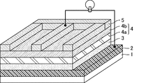
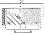
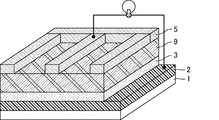
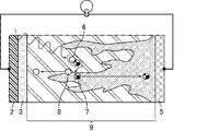
- a power generation mechanism of a PN junction type organic semiconductor solar cell and a bulk heterojunction type organic semiconductor solar cell will be described below with reference to FIGS. 59 and 60 are schematic views of a PN junction type organic semiconductor solar cell, FIG. 59 is a schematic perspective view, and FIG. 60 is a schematic cross-sectional view showing a power generation mechanism.
- 61 and 62 are schematic views of a bulk heterojunction type organic semiconductor solar cell, FIG. 61 is a schematic perspective view, and FIG. 62 is a schematic cross-sectional view showing a power generation mechanism.
- the PN junction type organic semiconductor solar cell includes a support substrate 1 such as a glass substrate, an anode 2, a hole transport layer 3, a photoelectric conversion layer 4, and a cathode 5.
- the photoelectric conversion layer 4 includes two layers in which a p-type organic semiconductor layer 4a and an n-type organic semiconductor layer 4b are stacked.
- An anode 2 is formed on the glass substrate 1, a hole transport layer 3 is formed on the anode 2, a p-type organic semiconductor layer 4 a is formed on the hole transport layer 3, and the p-type organic semiconductor layer 4 a
- the n-type organic semiconductor layer 4b is formed, and the cathode 5 is formed on the n-type organic semiconductor layer 4b.
- the interface (pn junction interface) between the p-type organic semiconductor layer 4a and the n-type organic semiconductor layer 4b.
- excitons 6 in which electrons 7 and holes 8 are paired are generated.
- the excitons 6 reach the pn junction interface, they are separated into electrons 7 and holes 8 and move to the cathode 5 and the anode 2, respectively. Such a movement of electric charge generates a current.
- a bulk heterojunction type organic semiconductor solar cell includes a p-type organic semiconductor material instead of a photoelectric conversion layer in which a p-type organic semiconductor layer and an n-type organic semiconductor layer are stacked. It has a single-layer photoelectric conversion layer 9 mixed with an n-type organic semiconductor material.
- the configuration other than the photoelectric conversion layer 9 is the same as that of the PN junction type organic semiconductor solar cell.
- the photoelectric conversion layer 9 has a large area at the pn junction interface because a p-type organic semiconductor material and an n-type organic semiconductor material are mixed. Therefore, when the photoelectric conversion layer 9 is irradiated with excitation light (for example, sunlight), there is a high probability that the excitons 6 reach the pn junction interface, and the excitons 6 are easily separated into electrons 7 and holes 8. Therefore, the photoelectric conversion efficiency is high.
- excitation light for example, sunlight
- Patent Document 1 Non-Patent Documents 1 and 2.
- polarization characteristics can be imparted by rubbing the p-type organic semiconductor layer.
- Display devices such as a liquid crystal display device require power supply from the outside such as a power source and a battery in order to display an image. For this reason, it cannot be used in areas where power infrastructure is not established, and it cannot be used when external power is not supplied due to a disaster or the like. Further, in recent years, awareness of environmental energy has increased, and therefore a self-powered display that generates power by the display device itself is required.
- a product combining a silicon solar cell and a display device has been proposed for a long time.
- a silicon-based solar cell it is necessary to dispose the solar cell behind the display surface or to arrange the display surface and the solar cell side by side.
- silicon-based solar cells do not transmit light, if a solar cell is disposed on the back side of the display surface, display and power generation cannot be performed simultaneously. Further, when the display surface and the solar cell are arranged side by side, a large installation area is required.
- the present invention has been made in view of the above-described present situation, and has a power generation function and a polarization characteristic, and a polarizing element having an efficient configuration, a manufacturing method of the polarizing element, a liquid crystal display device having the polarizing element, and An object of the present invention is to provide a method for manufacturing the liquid crystal display device.
- the present inventors have studied a configuration that can generate power simultaneously with display without complicating the configuration. Then, paying attention to the point that an organic semiconductor solar cell can impart polarization characteristics by performing a certain treatment, the polarizing element included in the liquid crystal display device is replaced with a solar cell having polarization characteristics. Thus, it has been found that a power generation function can be imparted to the polarizing element without complicating the configuration. In addition, since the organic semiconductor solar cell can easily ensure translucency, even if it is placed so as to overlap with the display surface, there is little demerit that light is blocked.
- the present inventors have conducted further studies, and even when the polarization characteristics are imparted to the bulk heterojunction type organic semiconductor layer instead of the PN junction type organic semiconductor layer, the same method may be used. It was confirmed that the bulk heterojunction type has better polarization characteristics than the PN junction type.
- One embodiment of the present invention includes a supporting substrate, a first electrode, a second electrode, an organic semiconductor layer disposed between the first electrode and the second electrode, and the first electrode A first carrier transport layer disposed between an electrode and the organic semiconductor layer and / or a second carrier transport layer disposed between the organic semiconductor layer and the second electrode.
- the support substrate, the first electrode, and the second electrode are arranged in this order, and the organic semiconductor layer is a single layer organic semiconductor layer of a bulk heterojunction type, and the first carrier transport At least one of the layer, the organic semiconductor layer, and the second carrier transport layer is a polarizing element having polarization characteristics.
- the first electrode may be an anode or a cathode.
- the second electrode may be an anode or a cathode.
- the first carrier transport layer may be a hole transport layer or an electron transport layer.
- the second carrier transport layer may be a hole transport layer or an electron transport layer.
- the configuration of the polarizing element of the present invention is not particularly limited by other components as long as such components are formed as essential.
- the application of the polarizing element of the present invention is not limited, and can be applied to optical elements such as polarizing sunglasses, polarizing lenses, and polarizing filters in addition to the liquid crystal display device.
- the first electrode is an anode
- the second electrode is a cathode
- the first carrier transport layer is a hole transport layer
- the second carrier transport layer is
- the first electrode is a cathode
- the second electrode is an anode
- the first carrier transport layer is an electron transport layer
- the configuration (i) is also referred to as a normal type (Normal type)
- the configuration (ii) is also referred to as an inverted type (Inverted type).
- the surface of the organic semiconductor layer may have irregularities.
- the unevenness may be a linear groove in plan view.
- the groove width is preferably 1 to 1000 nm
- the interval between adjacent grooves is preferably 10 to 10000 nm
- the depth of the groove is preferably 1 to 100 nm.
- the surface of the first carrier transport layer and / or the surface of the second carrier transport layer may have irregularities.
- the unevenness may be a linear groove in plan view.
- the groove width is preferably 1 to 1000 nm
- the interval between adjacent grooves is preferably 10 to 10000 nm
- the depth of the groove is preferably 1 to 100 nm.
- the surface of the support substrate may have irregularities.
- the unevenness may be a linear groove in plan view.
- the width of the groove is preferably 100 to 1000 nm, the interval between adjacent grooves is preferably 100 to 10000 nm, and the depth of the groove is preferably 10 to 300 nm.
- the second electrode may have a plurality of parts formed of different materials.
- the second electrode may have a light-transmitting part and a light-shielding part.
- the second electrode may have a grid-like electrode portion and a comb-like electrode portion.
- the second electrode has a portion having a greater thickness and a portion having a smaller thickness, and the portion having the smaller thickness is made of a material having a higher electrical conductivity than the portion having the greater thickness. Preferably it is.
- the second electrode is a cathode and has a thicker part and a thinner part.
- the thinner part is a material having a work function smaller than that of the thicker part. It is preferable to be configured.
- the second electrode is an anode and has a thicker part and a thinner part, and the thinner part is made of a material having a work function larger than that of the thicker part. It is preferable to be configured.
- Another embodiment of the present invention includes a step of forming a first electrode on a supporting substrate, a step of forming a bulk heterojunction type single-layer organic semiconductor layer on the first electrode, and the organic Forming a second electrode on the semiconductor layer, forming a first carrier transport layer between the first electrode and the organic semiconductor layer, and / or the organic semiconductor layer and the first Forming a second carrier transport layer between the two electrodes, wherein at least one of the first carrier transport layer, the organic semiconductor layer, and the second carrier transport layer is a polarization property. It is a manufacturing method of the polarizing element which has these.
- the first electrode may be an anode or a cathode.
- the second electrode may be an anode or a cathode.
- the first carrier transport layer may be a hole transport layer or an electron transport layer.
- the second carrier transport layer may be a hole transport layer or an electron transport layer.
- the method for producing a polarizing element of the present invention is not particularly limited by other steps as long as such steps are essential.
- the first electrode is an anode
- the second electrode is a cathode
- the first carrier transport layer is a hole transport layer
- the second carrier transport layer is
- the first electrode is a cathode
- the second electrode is an anode
- the first carrier transport layer is an electron transport layer
- the configuration (i) is also referred to as a normal type (Normal type)
- the configuration (ii) is also referred to as an inverted type (Inverted type).
- the step of forming irregularities on the surface of the organic semiconductor layer may be a step of rubbing the surface of the organic semiconductor layer.
- the groove width is preferably 1 to 1000 nm
- the interval between adjacent grooves is preferably 10 to 10000 nm
- the groove depth is preferably 1 to 100 nm.
- the step of forming irregularities on the surface of the organic semiconductor layer may be a step of forming linear grooves on the surface of the organic semiconductor layer in plan view using photolithography.
- the groove width is preferably 100 to 1000 nm
- the interval between adjacent grooves is preferably 100 to 10,000 nm
- the groove depth is preferably 10 to 100 nm.
- An example of the step of forming the organic semiconductor layer may be a step of applying the organic semiconductor material while moving the support substrate in one direction.
- a step of extending the organic semiconductor layer may be provided between the step of forming the organic semiconductor layer and the step of forming the second electrode.
- the step of forming irregularities on the surface of the first carrier transport layer may be a step of rubbing the surface of the first carrier transport layer.
- the groove width is preferably 1 to 1000 nm
- the interval between adjacent grooves is preferably 10 to 10000 nm
- the groove depth is preferably 1 to 100 nm.
- the step of forming irregularities on the surface of the first carrier transport layer may be a step of forming linear grooves on the surface of the first carrier transport layer in plan view using photolithography.
- the groove width is preferably 100 to 1000 nm
- the interval between adjacent grooves is preferably 100 to 10,000 nm
- the groove depth is preferably 10 to 100 nm.
- the step of forming irregularities on the surface of the second carrier transport layer may be a step of rubbing the surface of the second carrier transport layer.
- the groove width is preferably 1 to 1000 nm
- the interval between adjacent grooves is preferably 10 to 10000 nm
- the groove depth is preferably 1 to 100 nm.
- the step of forming irregularities on the surface of the second carrier transport layer may be a step of forming linear grooves on the surface of the second carrier transport layer in plan view using photolithography.
- the groove width is preferably 100 to 1000 nm
- the interval between adjacent grooves is preferably 100 to 10,000 nm
- the groove depth is preferably 10 to 100 nm.
- the number of rubbing is preferably 15 to 160 times, more preferably 40 ⁇ 160 times, more preferably 80 to 160 times.
- the step of forming irregularities on the surface of the support substrate may be a step of forming linear grooves on the surface of the support substrate in plan view.
- the width of the groove is preferably 100 to 1000 nm, the interval between adjacent grooves is preferably 100 to 10000 nm, and the depth of the groove is preferably 10 to 300 nm.
- Another embodiment of the present invention includes a pair of substrates, a liquid crystal layer sandwiched between the pair of substrates, A pair of polarizing elements, and at least one of the pair of polarizing elements is any one of the polarizing elements of the present invention, and on one surface of the pair of substrates opposite to the liquid crystal layer side.
- a liquid crystal display device first liquid crystal display device of the present invention
- the configuration of the first liquid crystal display device of the present invention is not particularly limited by other components as long as such components are essential.
- Either one of the pair of substrates may have a black matrix, and at least a part of the second electrode of the polarizing element may be disposed so as to overlap the black matrix.
- the portion of the second electrode that overlaps with the black matrix may be thicker than the portion that does not overlap with the black matrix.
- the portion of the second electrode that does not overlap with the black matrix may have a light transmitting property.
- the second electrode may be positioned between the first electrode and the liquid crystal layer.
- Another embodiment of the present invention includes a pair of substrates and a liquid crystal layer sandwiched between the pair of substrates, and at least one of the pair of substrates includes a liquid crystal display device including the above polarizing element ( 2 is a second liquid crystal display device of the present invention.
- the configuration of the second liquid crystal display device of the present invention is not particularly limited by other components as long as such components are essential.
- any one of the substrates may have a black matrix, and at least a part of the second electrode of the polarizing element may be disposed so as to overlap the black matrix.
- the portion of the second electrode that overlaps with the black matrix may be thicker than the portion that does not overlap with the black matrix.
- the portion of the second electrode that does not overlap with the black matrix may have a light transmitting property.
- the second electrode may be positioned between the first electrode and the liquid crystal layer.
- a polarizing element manufactured by the method for manufacturing a polarizing element according to any one of the present invention and the polarizing element manufactured by the step of manufacturing the polarizing element is sandwiched between liquid crystal layers. And a step of disposing one of a pair of substrates on a surface opposite to the liquid crystal layer (a method for producing a first liquid crystal display device of the present invention).
- the method for producing the first liquid crystal display device of the present invention is not particularly limited by other steps as long as such steps are essential.
- a method for manufacturing a liquid crystal display device which includes a step of manufacturing a polarizing element on at least one of a pair of substrates sandwiching a liquid crystal layer, by the method for manufacturing a polarizing element according to any one of the present invention. (The manufacturing method of the 2nd liquid crystal display device of this invention).
- the method for producing the second liquid crystal display device of the present invention is not particularly limited by other steps as long as such steps are essential.
- a polarizing element excellent in an electric power generation function and a polarization characteristic and provided with an efficient structure, and a liquid crystal display device provided with this polarizing element are obtained.
- FIG. 1 is a schematic cross-sectional view of a polarizing plate including a polarizing element according to Embodiment 1.
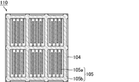
- FIG. 2 is a schematic plan view of a polarizing plate including the polarizing element according to Embodiment 1.
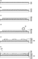
- FIG. 3 is a schematic diagram illustrating a manufacturing process of a polarizing plate including the polarizing element according to the first embodiment.
- FIG. 6 is a schematic plan view of a polarizing element according to application form 1.
- FIG. 6 is a schematic plan view of a polarizing element according to application form 1. The schematic diagram showing the manufacturing process (1st manufacturing process) of the cathode of the polarizing element which concerns on the application form 1.
- FIG. 1 is a schematic cross-sectional view of a polarizing plate including a polarizing element according to Embodiment 1.
- FIG. 2 is a schematic plan view of a polarizing plate including the polarizing element according to Embodiment 1.
- FIG. 3 is a schematic diagram
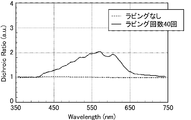
- FIG. 3 is a graph showing the dichroic ratio of the polarizing element according to Example 1.
- 6 is a graph showing the dichroic ratio of the polarizing element according to Comparative Example 1.
- FIG. 4 is a schematic cross-sectional view of a polarizing plate including a polarizing element according to Embodiment 2.
- FIG. 5 is a schematic diagram illustrating a manufacturing process of a polarizing plate including a polarizing element according to Embodiment 2.
- FIG. 5 is a schematic diagram illustrating a manufacturing process of a polarizing plate including a polarizing element according to Embodiment 2.
- FIG. 6 is a schematic cross-sectional view of a polarizing plate including a polarizing element according to Embodiment 3.
- FIG. 6 is a schematic plan view of a polarizing element according to Embodiment 3.
- FIG. 6 is a schematic plan view of a polarizing element according to Embodiment 3.
- FIG. 6 is a schematic plan view of a polarizing element according to Embodiment 3.
- FIG. 6 is a schematic cross-sectional view showing a power generation mechanism of a polarizing element according to a second embodiment.
- FIG. 6 is an energy band diagram of a polarizing element according to Embodiment 2.
- FIG. 6 is a schematic cross-sectional view showing a power generation mechanism of a polarizing element according to a third embodiment.
- FIG. 6 is an energy band diagram of a polarizing element according to Embodiment 3.
- FIG. 6 is a schematic diagram illustrating a manufacturing process of a polarizing plate including a polarizing element according to Embodiment 3.
- FIG. 6 is a schematic diagram illustrating a manufacturing process of a polarizing plate including a polarizing element according to Embodiment 3.
- 5 is a schematic cross-sectional view of a polarizing plate including a polarizing element according to Embodiment 4.
- FIG. 6 is a schematic diagram illustrating a manufacturing process of a polarizing plate including a polarizing element according to Embodiment 4.
- 6 is a schematic cross-sectional view of a polarizing plate including a polarizing element according to Embodiment 5.
- FIG. 5 is a schematic diagram illustrating a manufacturing process of a polarizing plate including a polarizing element according to Embodiment 3.
- 5 is a schematic cross-sectional view of a polarizing
- FIG. 6 is a schematic diagram illustrating a manufacturing process of a polarizing plate including a polarizing element according to Embodiment 5.
- 9 is a schematic cross-sectional view of a polarizing plate including a polarizing element according to Embodiment 6.
- FIG. 10 is a schematic diagram illustrating a manufacturing process of a polarizing plate including a polarizing element according to Embodiment 6.
- 10 is a schematic cross-sectional view of a polarizing plate including a polarizing element according to Embodiment 7.
- FIG. FIG. 10 is a schematic diagram illustrating a manufacturing process of a polarizing plate including a polarizing element according to Embodiment 7.
- FIG. 10 is a schematic cross-sectional view of a polarizing plate including a polarizing element according to Embodiment 8.
- FIG. 10 is a schematic diagram illustrating a manufacturing process of a polarizing plate including a polarizing element according to Embodiment 8.
- 10 is a schematic cross-sectional view of a polarizing plate including a polarizing element according to Embodiment 9.
- FIG. 10 is a schematic diagram illustrating a manufacturing process of a polarizing plate including a polarizing element according to Embodiment 9.
- FIG. 10 is a schematic diagram illustrating a manufacturing process of a polarizing plate including a polarizing element according to Embodiment 9.
- FIG. 10 is a schematic cross-sectional view of a polarizing plate including a polarizing element according to Embodiment 10.
- FIG. 10 is a schematic diagram illustrating a manufacturing process of a polarizing plate including the polarizing element according to the tenth embodiment.
- FIG. 10 is a schematic diagram illustrating a manufacturing process of a polarizing plate including a polarizing element according to Embodiment 10.
- 12 is a schematic cross-sectional view of a polarizing plate including a polarizing element according to Embodiment 11.
- FIG. 12 is a schematic diagram illustrating a manufacturing process of a polarizing plate including a polarizing element according to Embodiment 11.
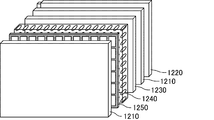
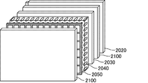
- FIG. 18 is a schematic perspective view of a liquid crystal display device according to a twelfth embodiment.
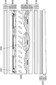
- FIG. 16 is a schematic cross-sectional view of a liquid crystal display device according to Embodiment 12.
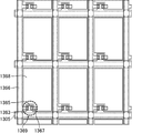
- FIG. 18 is a schematic plan view of a TFT substrate of a liquid crystal display device according to Embodiment 12.
- FIG. 18 is a schematic plan view of a color filter substrate of a liquid crystal display device according to Embodiment 12.
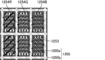
- FIG. 18 is a schematic plan view in which the position of the cathode is added to the schematic plan view of the color filter substrate of the liquid crystal display device according to Embodiment 12.
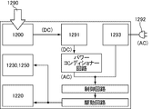
- FIG. 25 is a diagram illustrating a power supply path in a liquid crystal display device according to a twelfth embodiment.
- FIG. 20 is a schematic perspective view of a liquid crystal display device according to a thirteenth embodiment.
- FIG. 18 is a schematic cross-sectional view of a liquid crystal display device according to Embodiment 13.
- 14 is a schematic plan view of a TFT substrate of a liquid crystal display device according to Embodiment 13.
- FIG. FIG. 18 is a schematic plan view of a color filter substrate of a liquid crystal display device according to Embodiment 13.
- FIG. 18 is a schematic diagram showing a manufacturing process of a TFT substrate of a liquid crystal display device according to Embodiment 13.
- FIG. 18 is a schematic diagram showing a manufacturing process of a TFT substrate of a liquid crystal display device according to Embodiment 13.
- FIG. 19 is a schematic diagram illustrating a manufacturing process of a color filter substrate of a liquid crystal display device according to Embodiment 13.
- FIG. 18 is a schematic perspective view of a liquid crystal display device according to a fourteenth embodiment.
- FIG. 18 is a schematic cross-sectional view of a liquid crystal display device according to a fourteenth embodiment.
- FIG. 6 is a schematic cross-sectional view of a liquid crystal display device according to an application form 2. The plane schematic diagram which added the position of the cathode with respect to the plane schematic diagram of the color filter substrate of the liquid crystal display device which concerns on the application form 2.
- FIG. 19 is a schematic diagram illustrating a manufacturing process of a color filter substrate of a liquid crystal display device according to Embodiment 13.
- FIG. 18 is a schematic perspective view of a liquid crystal display device according to a fourteenth embodiment.
- FIG. 10 is a schematic cross-sectional view of a liquid crystal display device according to an application mode 3.
- FIG. 10 is a schematic plan view of a color filter substrate of a liquid crystal display device according to an application form 3.
- FIG. 10 is a schematic plan view of a color filter substrate of a liquid crystal display device according to an application form 3.
- the perspective schematic diagram of a PN junction type organic semiconductor solar cell The cross-sectional schematic diagram which shows the electric power generation mechanism of the solar cell of a PN junction type organic semiconductor type
- Each polarizing element may be used as a “power generation element” that can take out electrons and holes generated when exposed to light as a direct current, such as a solar cell,
- a photodiode, a CCD (Charged Coupled Device) using the photodiode, or a CMOS image sensor holds electrons generated when light strikes inside the semiconductor layer, and the intensity of light (light It is also possible to use it as a “light receiving element” capable of taking out an electrical signal corresponding to the signal) to the outside.
- Embodiment 1 In Embodiment 1, the normal type (normal type) has only the hole transport layer (first carrier transport layer) as the carrier transport layer, and the organic semiconductor layer is uneven by rubbing to impart polarization characteristics. The form will be described.
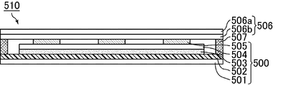
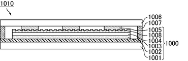
- FIG. 1 and 2 are schematic views of a polarizing plate including a polarizing element according to Embodiment 1, FIG. 1 is a schematic sectional view, and FIG. 2 is a schematic plan view.
- a polarizing element 100 according to Embodiment 1 includes a support substrate 101, an anode (first electrode) 102, a hole transport layer (first carrier transport layer) 103, an organic semiconductor layer 104, and And a cathode (second electrode) 105, which are laminated in this order.
- the polarizing element 100 is attached to the counter substrate 106 with a sealing material 107, and the combination of the polarizing element 100, the sealing material 107, and the counter substrate 106 constitutes one polarizing plate 110.
- the anode 102 is translucent and has a flat plate shape.
- the shape of the cathode 105 as shown in FIG. 2, the shape which is a grid
- the organic semiconductor layer 104 has polarization characteristics (optical anisotropy). Polarization characteristics should be expressed as the transmittance ratio between the case where two polarizing elements are arranged in parallel Nicols so that the polarization axes are parallel to each other and the case where they are arranged in crossed Nicols so that the polarization axes are orthogonal to each other. This ratio of transmittance is also called “dichroic ratio”. In general, when the polarizing element is used in a liquid crystal display device or the like, it can perform a monochrome display with a dichroic ratio of 2 or more, and a higher dichroic ratio can provide a better monochrome display. . In this specification, “having polarization characteristics” refers to a case where the dichroic ratio at a wavelength component of 550 nm is 2 or more.
- the organic semiconductor layer 104 is a bulk heterojunction single-layer organic semiconductor layer formed by mixing a p-type organic semiconductor material and an n-type organic semiconductor material.
- the organic semiconductor layer 104 is a photoelectric conversion layer.
- When the excitons reach the pn junction interface they are separated into electrons and holes (holes), and the electrons move to the cathode 105 and the holes move to the anode 102.
- Such a movement of electric charge generates a current.
- the diffusion length of electrons and holes is as short as several hundreds nm. Therefore, in a PN junction type organic semiconductor layer, the probability of excitons reaching the pn junction interface is low. Since the bulk heterojunction type has a large area at the pn junction interface, the probability of excitons reaching the pn junction interface is high. Accordingly, the photoelectric conversion efficiency is improved.
- the cathode 105 is preferably made of a metal having a small work function that easily collects electrons efficiently.
- Aluminum (Al, work function: 4.3 eV), silver (Ag, work function: 4.3 to 4.7 eV) Etc.) are preferably used.
- the cathode 105 is preferably an electrode having a light-transmitting property or a semi-light-transmitting property. Can be granted.
- a translucent electrode refers to one having a transmittance of 60 to 100%, and a semi-transparent electrode refers to one having a transmittance of 30 to 60%.
- the anode 102 is preferably a transparent electrode having a large work function that easily collects holes efficiently, and indium-tin-oxide (ITO, work function 4.8 eV) or the like is preferably used.
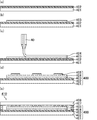
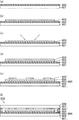
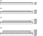
- FIG. 3 is a schematic diagram illustrating a manufacturing process of a polarizing plate including the polarizing element according to the first embodiment.
- an anode 102 is formed on a support substrate 101 by a sputtering method, a vacuum evaporation method, an inkjet method, or a printing method.
- the support substrate 101 is an insulating substrate, and a glass substrate, a plastic substrate, a film sheet, a substrate in which a film sheet is attached to a glass substrate, or the like can be used.
- the anode 102 can be formed using indium tin oxide (ITO), carbon nanotubes (CNT), graphene, an ink or a solution containing them, or the like.
- the hole transport layer 103 is formed on the anode 102 by spin coating, slit coating, vapor deposition, or the like.
- annealing treatment heat treatment
- a nitrogen-substituted glove box in order to further expel moisture and oxygen in the hole transport layer 103.
- the hole transport layer 103 includes polyaniline, polyphenylene vinylene, polythiophene, polypyrrole, polyparaphenylene, polyacetylene, triphenyldiamine (TPD), polyethylene dioxythiophene (PEDOT), polyethylene dioxythiophene-polystyrene doped with (doped) impurities. It can be formed using sulfonic acid (PEDOT: PSS), polysilane, or the like.
- the impurity is preferably a counter ion such as polystyrene sulfonic acid from the viewpoint of neutralizing the charge.
- a thermoplastic resin such as a polyester resin or a hydrophilic polymer such as polyvinyl alcohol is preferable.
- an organic semiconductor material is applied on the hole transport layer 103 by a spin coat method, a slit coat method, or the like to form an organic semiconductor layer 104.
- the organic semiconductor layer 104 is formed using an organic semiconductor material in which a p-type organic semiconductor material and an n-type organic semiconductor material are mixed.
- Examples of p-type organic semiconductor materials include copper phthalocyanine, poly (2-methoxy, 5- (2′-ethyl-hexyloxy) -1,4-phenylene vinylene (MEH-PPV), and poly (2-methoxy-5- (3′-7′-dimethyloctyloxy) -1,4-phenylene vinylene (MDMO-PPV), poly (3-hexylthiophene) (P3HT), etc.
- Examples of the n-type organic semiconductor material include perylene diimide derivatives, fullerene, phenyl C 61 butyric acid methyl ester (PCBM), or the like fullerene derivatives such Saimefu (SIMEF) and the like.
- the surface of the organic semiconductor layer 104 is rubbed using a rubbing roller 10.
- the number of rubbing times is 15 times or more, and polarization characteristics can be imparted to the organic semiconductor layer. The larger the number of rubbing times, the higher the value of the dichroic ratio.
- the rubbing frequency is preferably 15 to 160 times, more preferably 40 to 160 times, and still more preferably 80 to 160 times.
- the rubbing treatment may be performed while heating.
- the cathode 105 is formed on the organic semiconductor layer 104 by a sputtering method, a vacuum evaporation method, an ink jet method, or a printing method. Thereby, the polarizing element 100 is completed.
- the cathode 105 can be formed using aluminum (Al), silver (Ag), gold (Au), carbon nanotubes (CNT), a carbon compound such as graphene, an ink or a solution containing them, or the like.
- the polarizing element 100 is completed.
- the completed polarizing element 100 may be annealed (heat treated) as necessary.
- the polarizing element 100 and the counter substrate 106 are bonded together with a sealant 107, and the anode 102, the hole transport layer 103, the organic semiconductor layer 104, and the cathode 105 are bonded to the support substrate 101. Sealing is performed between the counter substrate 106 and the counter substrate 106. Thereby, the hole transport layer 103 and the organic semiconductor layer 104 can be prevented from being exposed to the atmosphere.
- a glass substrate, a plastic substrate, a film sheet, or the like can be used as the counter substrate 106.
- a protective film made of an inorganic compound may be formed on the surface of the plastic substrate or film sheet.
- any of a material that is cured by irradiation with ultraviolet light, a material that is cured by heat, and a material that is cured by irradiation with heat and ultraviolet light may be used.
- the generated electromotive force can be charged to the power storage element.
- Whether or not the anode 102 and the cathode 105 are formed in the polarizing element 100 can be confirmed using a microscope. Whether at least one of the hole transport layer 103 and the organic semiconductor layer 104 has polarization characteristics is prepared by preparing a pair of polarizing plates 110 including the polarizing element 100 and measuring a dichroic ratio using a spectroscope. Can be confirmed. Moreover, it can be confirmed using a solar simulator whether the polarizing element 100 has a power generation function. Whether the polarizing element has an organic semiconductor layer and the organic semiconductor layer 104 is formed by mixing a p-type organic semiconductor material and an n-type organic semiconductor material is determined by X-ray photoelectron spectroscopy (XPS). ). Whether or not the organic semiconductor layer 104 is a single layer can be confirmed using a scanning electron microscope (SEM: Scanning Electron Microscope) or a transmission electron microscope (TEM: Transmission Electron Microscope).
- SEM Scanning Electron Microscope
- the first embodiment it is possible to obtain a polarizing element having a power generation function and excellent polarization characteristics.
- the rubbing method established as a mass production technique it is possible to increase the area and mass production.
- the application form 1 is an example of a polarizing plate including the polarizing element according to the first embodiment, and is a form that pays particular attention to the shape of the cathode 105.
- 4 and 5 are schematic plan views of the polarizing element according to Application Mode 1.
- FIG. As shown in FIGS. 4 and 5, in the application mode 1, the cathode 105 includes a grid-like electrode portion 105b and a comb-like electrode portion 105a surrounded by the grid-like electrode portion 105b.
- the comb-like electrode portion 105a is electrically connected to the grid-like electrode portion 105b.
- the diffusion length of electrons and holes separated at the pn junction interface is as short as several hundred nm.
- the cathode 105 is preferably formed as wide as possible. In order to increase the area, not only the grid-like electrode portion but also the comb-like electrode It is preferable to further have a portion.
- a plurality of comb-like electrode portions 105a are provided, and are formed so that they are alternately meshed with each other at a predetermined interval.
- the comb-shaped electrode portion 105a may be linear as shown in FIG. 4, or may have a plurality of bent portions as shown in FIG.
- the comb-shaped electrode portion 105a is a thin film having a low work function, high conductivity, and high efficiency in order to efficiently collect electrons generated in the organic semiconductor layer 104 while increasing the transmittance of the polarizing element. preferable.
- the thickness of the grid-like electrode portion 105b is preferably larger than the thickness of the comb-like electrode portion 105a.
- the grid-like electrode portion 105b includes aluminum (Al, work function: 4.3 eV), silver (Ag, work function: 4.3 to 4.7 eV) having a work function (small work function) suitable for electron collection. Etc.) are preferably used. Since the wiring resistance can be lowered by increasing the film thickness of the grid-like electrode portion 105b, electrons can be easily collected.
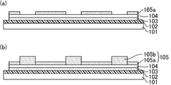
- the cathode is formed by a first manufacturing process or a second manufacturing process described later, instead of the process shown in FIG. 6 and 7 are schematic views showing the manufacturing process of the cathode of the polarizing element according to the application form 1.
- FIG. 6 shows the first manufacturing process
- FIG. 7 shows the second manufacturing process.
- a mask vapor deposition method or a sputtering method is used on the organic semiconductor layer 104 to form a portion other than the portion where the lattice-like electrode portion 105b is formed later. Then, the comb-like electrode portion 105a is formed. Next, as shown in FIG. 6B, a grid-like electrode portion 105b is formed in a portion where the comb-like electrode portion 105a is not formed by using a mask vapor deposition method or a sputtering method.
- a comb-like electrode portion 105a is formed on the entire surface of the organic semiconductor layer 104 by using a mask vapor deposition method or a sputtering method. Thereafter, as shown in FIG. 7B, a grid-like electrode portion 105b is formed on the comb-like electrode portion 105a by using a mask vapor deposition method.
- the thickness of the comb-like electrode portion 105a is preferably 1 to 50 nm, and more preferably 10 to 30 nm.
- the thickness of the grid-like electrode portion 105b is preferably 100 to 400 nm in the first manufacturing process, more preferably 100 to 200 nm, and preferably 100 to 400 nm in the second manufacturing process. More preferably, it is 100 to 200 nm.
- different materials can be selected for the comb-like electrode portion 105a and the lattice-like electrode portion 105b, and the electrons generated in the organic semiconductor layer 104 can be increased while increasing the transmittance of the polarizing element 100. It can be collected efficiently.
- a material having higher electrical conductivity for the comb-like electrode portion 105a than for the lattice-like electrode portion 105b is preferable to use.
- aluminum Al, conductivity: 37.4 ⁇ 10 6 S / m
- copper Cu, conductivity: 59 ⁇ 10 6 S / m
- silver Ag, conductivity: 61.4 ⁇ 10 6 S / m
- the thickness of the comb-like electrode portion 105a is smaller than the thickness of the grid-like electrode portion 105b. can do. Thereby, since the translucent thin film which raised the transmittance
- a material having a work function smaller than that of the grid-like electrode portion 105b for the comb-like electrode portion 105a is preferable to use.
- silver (Ag, work function: 4.3 to 4.7 eV) is used for the grid-like electrode portion 105b
- copper (Cu, work function: 4.7 eV) is used for the grid-like electrode portion 105b
- silver (Ag, work function: 4.3 to 4.7 eV) is used for the comb-like electrode portion 105a. ) May be used.
- the comb-like electrode portion 105a is made of a material having a work function smaller than that of the grid-like electrode portion 105b, so that the lattice-like electrode portion to which the electrons collected by the comb-like electrode portion 105a are connected is used. It can be efficiently transported to 105b (or an external terminal connected to it).
- a material having a higher conductivity and a lower work function than the grid-like electrode portion 105b for the comb-like electrode portion 105a.
- copper conductivity: 59 ⁇ 10 6 S / m, work function: 4.7 eV
- silver Ag, conductivity
- the comb-shaped electrode portion 105a is made of a metal having a higher electrical conductivity and a lower work function than the lattice-shaped electrode portion 105b, thereby reducing the thickness of the comb-shaped electrode portion 105a.
- the light transmittance can be increased by making the thickness smaller.
- electrons collected by the comb-like electrode portion 105a can be efficiently transported to the connected grid-like electrode portion 105b (or an external terminal connected thereto), so that the photoelectric conversion efficiency can be increased. .
- Example 1 In the following, Example 1 in which a polarizing plate including a polarizing element is produced in the same manner as in Embodiment 1 is shown.
- an ITO film was formed on the entire surface of the glass substrate by sputtering. Then, it baked at 200 degreeC. Thereafter, a resist having a desired pattern shape was formed using photolithography, and then the ITO film was etched with concentrated hydrochloric acid or ferric chloride to form an electrode pattern. Thereafter, the resist was stripped using a stripping solution.
- PEDOT polyethylenedioxythiophene-polystyrene sulfonic acid
- PEDOT PSS
- a spin coating method to form a PEDOT: PSS film having a thickness of 40 nm.
- PEDOT: PSS adhering to the area where the sealing material is applied, the electrode pad area, etc. is wiped off, heat treatment (annealing treatment) is performed at 120 ° C. for 10 minutes on a hot plate, and the solvent is removed to form a hole transport layer. did.
- an annealing treatment was performed at 180 ° C. for 5 minutes in a nitrogen-substituted glove box.
- P3HT poly (3-hexylthiophene)
- PCBM phenyl C 61 butyric acid methyl ester
- the substrate was placed on a hot plate heated to 150 ° C. in a glove box subjected to nitrogen substitution, and the surface of the organic semiconductor layer was rubbed in one direction with a rubbing cloth.
- the number of times of rubbing was 0 times, 15 times, and 40 times.
- An aluminum (Al) electrode having a thickness of 100 nm was formed on the rubbed organic semiconductor layer by a vacuum deposition method using a metal mask. Vacuum deposition was performed under the conditions of a degree of vacuum of 10 ⁇ 4 Pa and a deposition rate of 1 to 10 ⁇ / s. The Al electrode was formed in a lattice shape in plan view. Thereafter, annealing was performed at 150 ° C. for 20 minutes. Thus, a polarizing element was obtained.
- P3HT By performing the annealing treatment, P3HT accumulates due to the ⁇ - ⁇ interaction between the thiophene skeletons of P3HT, which is a ⁇ -conjugated polymer, and self-organization is promoted, thereby improving light absorption characteristics and hole mobility. it can.
- the annealing process causes aggregation of PCBM (fullerene derivative) used as the n-type organic semiconductor material and the self-organization of the polymers (P3HT and PCBM) tends to be hindered.
- a photocurable sealing resin was applied to the peripheral portion of the counter substrate (glass substrate) using a dispenser device, and bonded to the polarizing element.
- the portions other than the seal resin application part were masked, and the ultraviolet light was irradiated to the seal resin application part for 1 to 2 minutes to bond the polarizing element and the counter substrate.
- the number of rubbing was 0 times, 15 times, and 40 times. Prepared.
- a sample having a rubbing frequency of 0 and a rubbing frequency of 40 were prepared.
- the measurement of the dichroic ratio was performed by obtaining the ratio of the transmittance when arranged in parallel Nicols and the transmittance when arranged in crossed Nicols using a spectroscope. The measurement wavelength range was 350 to 750 nm.
- Example 1 shows a value 1.5 to 2 times higher than that of Comparative Example 1. It was.
- the polarization characteristics are improved as the number of rubbing is increased, and monochrome display is performed with the number of rubbing being 15 times. As a result, it was found that the polarization characteristics can be obtained. Furthermore, it was found that the polarization characteristics can be improved with a smaller number of rubbing times compared to the polarizing element according to Comparative Example 1 having two PN junction type organic semiconductor layers.
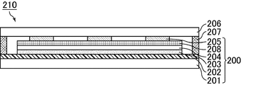
- the second embodiment is the same as the first embodiment except that a second carrier transport layer is further provided. That is, in a normal type (Normal type) polarizing element, a hole transport layer (first carrier transport layer) and an electron transport layer (second carrier transport layer) are provided as carrier transport layers, and organic semiconductor is rubbed. A mode in which unevenness is formed on the layer to impart polarization characteristics will be described.
- FIG. 10 is a schematic cross-sectional view of a polarizing plate including the polarizing element according to the second embodiment.
- the polarizing element 200 according to Embodiment 2 includes a support substrate 201, an anode (first electrode) 202, a hole transport layer (first carrier transport layer) 203, an organic semiconductor layer 204, and an electron. It has a transport layer (second carrier transport layer) 208 and a cathode (second electrode) 205, which are stacked in this order.
- the polarizing element 200 is attached to the counter substrate 206 with a sealing material 207, and the combination of the polarizing element 200, the sealing material 207, and the counter substrate 206 constitutes one polarizing plate 210.
- the organic semiconductor layer 204 is a single layer organic semiconductor layer of a bulk heterojunction type. In Embodiment 2, the organic semiconductor layer 204 has polarization characteristics (optical anisotropy).
- the electron transport layer (second carrier transport layer) 208 By disposing the electron transport layer (second carrier transport layer) 208 between the cathode (second electrode) 205 and the organic semiconductor layer 204, the efficiency of injecting electrons from the organic semiconductor layer 204 to the cathode 205 is increased. be able to.
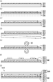
- FIG. 11A and FIG. 11B are schematic views illustrating a manufacturing process of a polarizing plate including the polarizing element according to the second embodiment.
- an anode 202 is formed on a support substrate 201 as shown in FIG. 11-1 (a), and holes are formed on the anode 202 as shown in FIG. 11-1 (b).
- a transport layer 203 is formed, an organic semiconductor layer 204 is formed on the hole transport layer 203 as shown in FIG. 11-1 (c), and an organic semiconductor layer 204 is formed as shown in FIG. 11-1 (d). Rubbing the surface of the.
- the electron transport layer 208 is formed on the organic semiconductor layer 204.
- an electron transport layer (second layer) is formed on the organic semiconductor layer 204 by a sol-gel method, a spin coating method, a slit coating method, a sputtering method, a vapor deposition method, or the like.
- Carrier transport layer) 208 is formed.
- the electron transporting layer 208 is formed using titanium oxide (TiO 2 ), zinc oxide (ZnO), lithium fluoride (LiF), or a solution in which these nanoparticles (particle diameter: about 1 to 30 nm) are dispersed. can do.
- the obtained sol is applied onto the organic semiconductor layer 204 by a spin coating method or a drop casting method, and is fired at 350 to 450 ° C. to form a microcrystalline TiO 2 thin film.
- the cathode 205 is formed on the electron transport layer 208, and the polarizing element 200 according to the second embodiment is completed.
- the polarizing element 200 and the counter substrate 206 are bonded to each other through a sealant 207, and the anode 202 and the positive substrate are interposed between the support substrate 201 and the counter substrate 206.
- the polarizing plate 210 is completed.
- the electron transport layer 208 since the electron transport layer 208 is provided, electrons generated in the organic semiconductor layer 204 can be efficiently collected.
- Embodiment 3 is different in the stacking order of the anode, the hole transport layer, the organic semiconductor layer, the electron transport layer, and the cathode on the support substrate (more specifically, the inverted type), and the anode and cathode.
- the second embodiment is the same as the second embodiment except that the material is different. That is, in the inverted type (inverted type), the carrier transport layer has a hole transport layer (first carrier transport layer) and an electron transport layer (second carrier transport layer), and the organic semiconductor layer is uneven by rubbing. A mode in which the polarization characteristics are imparted by forming the film will be described.
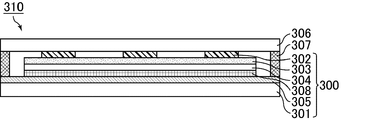
- FIG. 12 is a schematic cross-sectional view of a polarizing plate including the polarizing element according to the third embodiment.
- the polarizing element 300 according to Embodiment 3 includes a support substrate 301, a cathode (first electrode) 305, an electron transport layer (first carrier transport layer) 308, an organic semiconductor layer 304, and holes. It has a transport layer (second carrier transport layer) 303 and an anode (second electrode) 302, which are stacked in this order.
- the polarizing element 300 is attached to the counter substrate 306 with a sealing material 307, and the combination of the polarizing element 300, the sealing material 307, and the counter substrate 306 constitutes one polarizing plate 310.
- the organic semiconductor layer 304 is a single layer organic semiconductor layer of a bulk heterojunction type. In Embodiment 3, the organic semiconductor layer 304 has polarization characteristics (optical anisotropy).
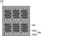
- FIGS. 13 to 15 are schematic plan views of the polarizing element according to the third embodiment.
- the shape of the anode 302 As an example of the shape of the anode 302, as shown in FIG. 13, a shape that is a lattice shape in a plan view can be cited as in FIG. 2 of the first embodiment. Further, as shown in FIGS. 14 and 15, the anode 302 includes a grid-like electrode portion 302 b and a comb-like electrode surrounded by the grid-like electrode portion as in FIGS. Portion 302a.
- the cathode 305 has translucency and has a flat plate shape.
- the shape of the anode 302 is the same as the shape of the cathode 105 of Embodiment 1
- the shape of the cathode 305 is the same as the shape of the anode 102 of Embodiment 1, but it is used for the anode 302 and the cathode 305.
- the electrode material is different from that of the first embodiment.
- the cathode 305 preferably uses a transparent electrode having a relatively small work function in order to perform a function of collecting electrons, and indium tin oxide (ITO, work function 4.8 eV) is preferably used. It is done.
- the anode 302 functions to collect holes, gold (Au, work function: 4.8 to 5.1 eV) having a relatively large work function is preferably used.
- Au work function: 4.8 to 5.1 eV
- a highly durable polarizing element can be obtained by using a metal such as Au that is stable even in the air and hardly oxidizes in the anode 302.
- the comb-shaped electrode portion 302a has high conductivity in order to efficiently collect holes generated in the organic semiconductor layer while increasing the transmittance of the polarizing element.
- a thin film is preferable.
- gold Au, work function: 4. 8 to 5.1 eV
- silver Ag, work function: 4.3 to 4.7 eV
- the thickness of the grid-like electrode portion 302b is preferably larger than the thickness of the comb-like electrode portion 302a.
- Gold Au, work function: 4.8 to 5.1 eV
- a work function suitable for collecting holes large work function
- the wiring resistance can be lowered, so that electrons can be easily collected.
- different materials can be selected for the comb-like electrode portion 302a and the lattice-like electrode portion 302b, and the transmittance of the polarizing element 300 is increased while the organic material is increased. Holes generated in the semiconductor layer 304 can be efficiently collected.
- a material having higher electrical conductivity for the comb-like electrode portion 302a than for the lattice-like electrode portion 302b is preferable to use.
- aluminum Al, conductivity: 37.4 ⁇ 10 6 S / m
- gold Au, conductivity: 45.5 ⁇ 10 6 S / m
- Copper Copper
- Cu conductivity: 59 ⁇ 10 6 S / m
- silver Ag, conductivity: 61.4 ⁇ 10 6 S / m
- the like may be used for the comb-shaped electrode portion 302a.
- the thickness of the comb-like electrode portion 302a is smaller than the thickness of the grid-like electrode portion 302b. can do. Thereby, since the translucent thin film which raised the transmittance
- a material having a work function larger than that of the grid-like electrode portion 302b for the comb-like electrode portion 302a.
- silver (Ag, work function: 4.3 to 4.7 eV) is used for the grid-like electrode portion 302b, and gold (Au, work function: 4.8 to 5.5) is used for the comb-like electrode portion 302a.
- gold Au, work function: 4.8 to 5.5
- comb-like electrode portion 302a 1 eV
- aluminum Al, work function: 4.3 eV
- silver Ag, work function: 4.3
- a grid-like electrode portion to which electrons collected by the comb-like electrode portion 302a are connected by using a material having a work function larger than that of the grid-like electrode portion 302b for the comb-like electrode portion 302a. It can be efficiently transported to 302b (or an external terminal connected to it).
- a material having a higher conductivity and a higher work function than the grid-like electrode portion 302b for the comb-like electrode portion 302a.
- aluminum Al, conductivity: 37.4 ⁇ 10 6 S / m, work function: 4.3 eV
- silver Ag, Conductivity: 61.4 ⁇ 10 6 S / m, work function: 4.3 to 4.7 eV
- copper Cu, conductivity: 59 ⁇ 10 6 S / m, work function: 4.7 to 5.1 eV
- Gold Au, conductivity: 45.5 ⁇ 10 6 S / m, work function: 4.8 to 5.1 eV
- the comb-like electrode portion 302a is made of a metal having a higher electrical conductivity and a larger work function than the lattice-like electrode portion 302b, so that the thickness of the comb-like electrode portion 302a can be reduced.
- the light transmittance can be increased by making the thickness smaller.
- electrons collected by the comb-like electrode portion 302a can be efficiently transported to the connected grid-like electrode portion 302b (or an external terminal connected thereto), so that the photoelectric conversion efficiency can be increased. .
- the inverted type Inverted type as in Embodiment 3, it is particularly preferable to have both a hole transport layer and an electron transport layer from the viewpoint of photoelectric conversion efficiency.
- the electron transport layer 308 between the first electrode (cathode) 305 and the organic semiconductor layer 304, holes are prevented from flowing to the cathode 305, and the second electrode (anode) 302 and the organic semiconductor layer 304 are prevented. This is because by providing the hole transport layer 303 therebetween, electrons can be prevented from flowing to the anode 302 and the photoelectric conversion efficiency can be prevented from decreasing.
- inverted type Inverted type as in the third embodiment, Au that is stable in the air and hardly oxidizes can be used for the anode 302 instead of highly corrosive Al or the like. Further, TiO 2 , ZnO, or the like that is stable in the air can be used for the electron transport layer 308 that is in contact with the cathode 305, and a highly durable polarizing element can be obtained.
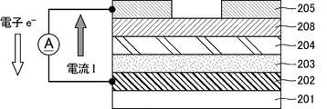
- FIG. 16 is a schematic cross-sectional view showing a power generation mechanism of the polarizing element according to the second embodiment
- FIG. 17 is an energy band diagram of the polarizing element according to the second embodiment
- FIG. 18 is a schematic cross-sectional view showing a power generation mechanism of the polarizing element according to the third embodiment
- FIG. 19 is an energy band diagram of the polarizing element according to the third embodiment.
- the polarizing element according to Embodiment 2 is a normal type (Normal type), the first electrode is the anode 202, the second electrode is the cathode 205, and the first carrier transport layer is the hole transport layer 203.
- the second carrier transport layer is an electron transport layer 208.
- an anode 202, a hole transport layer 203, an organic semiconductor layer 204, an electron transport layer 208, and a cathode 205 are stacked in this order.
- FIG. 17 is an energy band diagram when ITO is used for the anode 202, PEDOT: PSS for the hole transport layer 203, P3HT and PCBM for the organic semiconductor layer 204, TiO 2 for the electron transport layer 208, and Al for the cathode 205.
- HOMO Highest Occupied Molecular Orbital
- LUMO Large Unoccupied Molecular Orbital
- the polarizing element according to Embodiment 3 is an inverted type (Inverted type), the first electrode is a cathode 305, the second electrode is an anode 302, and the first carrier transport layer is an electron transport layer 308.
- the second carrier transport layer is the hole transport layer 303.
- the cathode 305, the electron transport layer 308, the organic semiconductor layer 304, the hole transport layer 303, and the anode 302 are stacked in this order.
- 19 is an energy band diagram when ITO is used for the cathode 305, TiO 2 is used for the electron transport layer 308, P3HT and PCBM are used for the organic semiconductor layer 304, PEDOT: PSS is used for the hole transport layer 303, and Au is used for the anode 302. .
- a metal having a low work function is used for the second electrode 205, and a metal having a high work function is used for the first electrode 202.
- the hole 8 moves to the anode 202. Due to such movement of electric charge, a current is generated from the anode (first electrode) 202 to the cathode (second electrode) 205.
- the inverted type inverted type
- a metal having a low work function is used for the first electrode 305
- a metal having a high work function is used for the second electrode 302.
- the hole 8 moves to the second electrode 302. Therefore, in the third embodiment, the direction of the current is opposite to that of the normal type (normal type) of the first embodiment, the first electrode 305 is a cathode, and the second electrode 302 is an anode.
- normal type has higher photoelectric conversion efficiency than the reverse type (inverted type) for reasons such as materials used for electrodes and organic semiconductors.
- FIGS. 20-1 and 20-2 are schematic views illustrating a manufacturing process of a polarizing plate including the polarizing element according to the third embodiment.
- a cathode 305 is formed on a support substrate 301 by a sputtering method, a vacuum evaporation method, an ink jet method, or a printing method.
- the cathode 305 is made of the material used as the material of the anode (first electrode) 102 in Embodiment 1, that is, indium tin oxide (ITO), carbon nanotube (CNT), graphene, ink or solution containing them, and the like. Can be formed.
- an electron transport layer 308 is formed on the cathode 305, and as shown in FIG. 20-1 (c), an organic semiconductor layer 304 is formed on the electron transport layer 308.
- the surface of the organic semiconductor layer 304 is rubbed to form a hole transport layer 303 on the organic semiconductor layer 304, as shown in FIG. 20-2 (e).
- the material, manufacturing method, and the like used for the electron transport layer 308 are the same as those in the second embodiment.
- the materials used for the organic semiconductor layer 304 and the hole transport layer 303, the manufacturing method, the method for rubbing the surface of the organic semiconductor layer 304, and the number of times are the same as those in the first embodiment.
- an anode 302 is formed on the hole transport layer 303 by sputtering, vacuum deposition, ink jet, or printing, and the polarization according to the third embodiment.
- the element 300 is completed.
- the anode 302 is a material used as the material of the cathode (second electrode) 105 in Embodiment 1, that is, carbon such as aluminum (Al), silver (Ag), gold (Au), carbon nanotube (CNT), graphene, or the like. It can be formed using a compound, an ink or a solution containing them, and the like. However, in Embodiment 3, it is preferable to use gold (Au) or the like having a higher work function as the anode 302 from the viewpoint of easily taking out generated holes.
- the polarizing element 300 and the counter substrate 306 are bonded to each other through a sealant 307, and the cathode 305 and the positive substrate 306 are interposed between the support substrate 301 and the counter substrate 306.
- the hole transport layer 303, the organic semiconductor layer 304, the electron transport layer 308, and the anode 302 is completed.
- Embodiment 3 a polarizing element with high durability can be obtained.
- Embodiment 4 is an embodiment except that it does not have a step of rubbing the organic semiconductor layer, and instead has a step of forming an organic semiconductor layer while stretching a mixed solution containing an organic semiconductor material. Same as 1. That is, in a normal type (Normal type) polarizing element, only a hole transport layer (first carrier transport layer) is provided as a carrier transport layer, and a polarization property is imparted by forming the organic semiconductor layer while stretching it. Is described.
- Normal type Normal type polarizing element
- FIG. 21 is a schematic cross-sectional view of a polarizing plate including the polarizing element according to the fourth embodiment.
- a polarizing element 400 according to Embodiment 4 includes a support substrate 401, an anode (first electrode) 402, a hole transport layer (first carrier transport layer) 403, an organic semiconductor layer 404, and And a cathode (second electrode) 405, which are stacked in this order.
- the polarizing element 400 is attached to the counter substrate 406 with a sealant 407, and the combination of the polarizing element 400, the sealant 407, and the counter substrate 406 constitutes one polarizing plate 410.
- the organic semiconductor layer 404 is a single layer organic semiconductor layer of a bulk heterojunction type. In Embodiment 4, the organic semiconductor layer 404 has polarization characteristics (optical anisotropy).
- the power generation mechanism is the same as that of the first embodiment.
- FIG. 22 is a schematic diagram illustrating a manufacturing process of a polarizing plate including the polarizing element according to the fourth embodiment.
- an anode 402 is formed on a support substrate 401 as shown in FIG. 22A, and a hole transport layer 403 is formed on the anode 402 as shown in FIG. Form.
- the organic semiconductor layer 404 is formed by, for example, a slit coat method. As shown in FIG. 22 (c), a mixed solution in which an organic semiconductor material is dissolved is applied by using a slit coater 40 while dropping on the hole transport layer 403 with a certain width from above. At this time, by applying the substrate while moving it, the mixed solution can be applied while being stretched, and the organic molecules in the organic semiconductor material can be oriented along the extending direction. As a result, an organic semiconductor layer 404 having polarization characteristics is obtained. In the fourth embodiment, the rubbing process is unnecessary.
- Embodiment 4 the p-type organic semiconductor material and the n-type organic semiconductor material listed in Embodiment 1 are dissolved in a solvent having a relatively high viscosity such as dioxane, cyclohexane, carbon tetrachloride, propanol, ethanol, ethylene glycol, and the like. Use the mixed solution.
- the mixed solution may further be mixed with an iodine solution containing iodine and potassium iodide.
- the iodine concentration in the iodine solution is preferably 0.01 to 1 wt%, and the potassium iodide concentration is preferably 0.01 to 10 wt%.
- poly (3-hexylthiophene) (P3HT) (1.25 wt%) and phenyl C 61 butyric acid methyl ester (PCBM) (1 wt%) are dissolved in chlorobenzene, Prepare a mixed solution. Furthermore, an iodine solution containing iodine (0.1 wt%) and potassium iodide (0.1 wt%) is mixed with the prepared mixed solution. Next, use a slit coater in a glove box where nitrogen substitution has been performed, apply the mixed solution while stretching the mixed solution by slowly moving the substrate while hanging the mixed solution on the hole transport layer with a certain width. An organic semiconductor layer having a thickness of about 150 nm is formed. Thereafter, a heat treatment (annealing treatment) is performed at 150 ° C. for 20 minutes on a hot plate, and the solvent is completely removed to form an organic semiconductor layer.
- annealing treatment annealing treatment
- a cathode 405 is formed on the organic semiconductor layer 404, and the polarizing element 400 according to the fourth embodiment is completed.
- the polarizing element 400 and the counter substrate 406 are bonded to each other through a sealant 407, and the anode 402 and the hole transport are provided between the support substrate 401 and the counter substrate 406.
- the polarizing plate 410 is completed.
- Embodiment 4 since rubbing is not performed, generation of dust and static electricity can be prevented, and the yield is high.
- the area can be easily increased, the number of steps is small, and the throughput is high.
- Embodiment 5 is the same as Embodiment 1 except that it does not have a step of rubbing the organic semiconductor layer, and instead, the organic semiconductor layer is uniaxially extended. That is, in a normal type (Normal type) polarizing element, only a hole transporting layer (first carrier transporting layer) is provided as a carrier transporting layer, and polarization characteristics are imparted by uniaxially extending the organic semiconductor layer. State.
- a normal type (Normal type) polarizing element only a hole transporting layer (first carrier transporting layer) is provided as a carrier transporting layer, and polarization characteristics are imparted by uniaxially extending the organic semiconductor layer. State.
- Normal type Normal type
- FIG. 23 is a schematic cross-sectional view of a polarizing plate including the polarizing element according to the fifth embodiment.
- a polarizing element 500 according to Embodiment 5 includes a support substrate 501, an anode (first electrode) 502, a hole transport layer (first carrier transport layer) 503, an organic semiconductor layer 504, and And a cathode (second electrode) 505, which are laminated in this order.
- the polarizing element 500 is attached to the counter substrate 506 with a sealant 507, and a combination of the polarizing element 500, the sealant 507, and the counter substrate 506 constitutes one polarizing plate 510.
- the support substrate 501 is a single-layer film made of a transparent film
- the counter substrate 506 is a laminated film made of a transparent film 506a and a protective film 506b formed of an inorganic compound.
- the organic semiconductor layer 504 is a single layer organic semiconductor layer of a bulk heterojunction type.
- the organic semiconductor layer 504 and the hole transport layer 504 have polarization characteristics (optical anisotropy).
- the power generation mechanism is the same as that of the first embodiment.
- FIG. 24 is a schematic diagram illustrating a manufacturing process of a polarizing plate including the polarizing element according to the fifth embodiment.
- the support substrate 501 is formed on the base substrate 580.
- the supporting substrate 501 is preferably made of a stretchable material such as an ultrathin plastic substrate or a film sheet.
- An example of the base substrate 580 is a glass substrate.
- the support substrate 501 can be formed as a film sheet by applying a transparent polyimide solution or the like on the base substrate 580 and baking it.
- the anode 502 is formed on the support substrate 501, and as shown in FIG. 24B, the hole transport layer 503 is formed on the anode 502, as shown in FIG.
- the organic semiconductor layer 504 is formed over the hole transport layer 503.
- an iodine solution may be used together as in the fourth embodiment.
- the support substrate 501 and the base substrate 580 are peeled off by laser irradiation or the like, and then, for example, as shown in FIG.
- the semiconductor layer 504 is uniaxially extended.
- the hole transport layer 503 is also uniaxially extended. Thereby, polarization characteristics can be imparted to the organic semiconductor layer 504 and the hole transport layer 503.
- the drawing ratio is preferably 1.2 to 7 times.
- Uniaxial distraction may use either a dry distraction method or a wet distraction method. Examples of the dry stretching method include an inter-roll stretching method, a heated roll stretching method, and a compression stretching method.
- the laminate prepared up to the organic semiconductor layer is immersed in a swelling bath, the laminate is swollen to perform distraction, and then immersed in an iodine solution containing iodine and potassium iodide. Then, it is dyed and further stretched while immersed in a crosslinking bath.
- a solution containing urea or thiourea can be used for the swelling bath, and a solution containing boric acid, borax or the like can be used for the crosslinking bath.
- a transparent polyimide solution is applied to a thickness of 10 to 30 ⁇ m on a glass substrate serving as a base substrate, and then the polyimide solution is baked to form a film sheet. Then, an anode including nanoparticles made of indium tin oxide (ITO) is formed on the entire surface of the film sheet using screen printing or gravure printing. Further, baking is performed at 200 to 300 ° C. to reduce the resistance of the ITO film.
- poly (3-hexylthiophene) (P3HT) (1.25 wt%) and phenyl C 61 butyric acid methyl ester (PCBM) (1 wt%) are dissolved in chlorobenzene to prepare a mixed solution.
- an iodine solution containing iodine (0.1 wt%) and potassium iodide (0.1 wt%) is mixed with the prepared mixed solution.
- the mixed solution adjusted as described above is applied onto the anode by a spin coating method to form the organic semiconductor layer 504.
- the laminated film formed up to the organic semiconductor layer is peeled off from the base substrate, and the peeled laminated film is passed through a hot roll in a glove box where nitrogen substitution is performed, and uniaxial stretching is performed by a dry stretching method.
- the cathode 505 is formed on the organic semiconductor layer 504, and the polarizing element 500 according to the fifth embodiment is completed.
- the polarizing element 500 and the counter substrate 506 are bonded to each other with a sealant 507, and the anode 502, the hole transport layer 503, and the like are interposed between the support substrate 501 and the counter substrate 506.
- the polarizing plate 510 is completed by sealing the organic semiconductor layer 504 and the cathode 505.
- the support substrate 501 is manufactured by forming a transparent film by the same method as the method of manufacturing the counter substrate 506 and further forming a protective film on the transparent film with an inorganic compound such as silicon nitride. can do.
- a polarizing element having a power generation function and high polarization characteristics can be obtained. Further, since rubbing is not performed, generation of dust and static electricity can be prevented, and the yield is high. Furthermore, since a thin and lightweight material such as plastic and a film sheet is used for the supporting substrate and the counter substrate, a light and highly flexible polarizing element can be obtained.
- Embodiment 6 is the same as Embodiment 1 except that it does not have a step of rubbing the organic semiconductor layer and instead forms a linear groove on the surface of the organic semiconductor layer in plan view. is there. That is, in a normal type (Normal type) polarizing element, it has only a hole transporting layer (first carrier transporting layer) as a carrier transporting layer, and a groove is formed on the surface of the organic semiconductor layer by laser irradiation, thereby polarizing characteristics. The form which gave is described.
- Normal type Normal type
- FIG. 25 is a schematic cross-sectional view of a polarizing plate including the polarizing element according to the sixth embodiment.
- a polarizing element 600 according to Embodiment 6 includes a support substrate 601, an anode (first electrode) 602, a hole transport layer (first carrier transport layer) 603, an organic semiconductor layer 604, and And a cathode (second electrode) 605, which are stacked in this order.
- the polarizing element 600 is attached to the counter substrate 606 with a sealant 607, and the combination of the polarizing element 600, the sealant 607, and the counter substrate 606 forms one polarizing plate 610.
- the organic semiconductor layer 604 is a bulk heterojunction single-layer organic semiconductor layer.
- linear grooves are formed on the surface of the organic semiconductor layer 604 in plan view, and have polarization characteristics (optical anisotropy).
- the power generation mechanism is the same as that of the first embodiment.
- FIG. 26 is a schematic diagram illustrating a manufacturing process of a polarizing plate including the polarizing element according to the sixth embodiment.
- an anode 602 is formed on a support substrate 601 as shown in FIG. 26A, and a hole transport layer 603 is formed on the anode 602 as shown in FIG. Form.
- laser irradiation is performed on the surface of the organic semiconductor layer 604 as shown in FIG. To form a linear groove in plan view.
- the laser irradiation method include a two-beam interference method and a phase mask method.
- the two-beam interference method is an optical lithography technique that matches the phase conditions and path lengths of two laser beams and transfers the periodic light intensity distribution (interference pattern) generated when they are superimposed onto a target member.
- the period of the interference pattern depends on the interference angle of the two light beams and the laser wavelength.
- a laser can form a one-dimensional or two-dimensional fine uneven pattern on the surface of the organic semiconductor layer 604.
- the width of the groove is preferably 100 to 1000 nm, more preferably 100 to 300 nm.
- the interval between adjacent grooves is preferably 100 to 10,000 nm, more preferably 100 to 1000 nm.
- the depth of the groove is preferably 10 to 100 nm, more preferably 50 to 100 nm.
- the cathode 605 is formed on the organic semiconductor layer 604, and the polarizing element 600 according to the sixth embodiment is completed.
- the polarizing element 600 and the counter substrate 606 are bonded to each other with a sealant 607, and the anode 602, the hole transport layer 603, and the like are interposed between the support substrate 601 and the counter substrate 606.
- the polarizing plate 610 is completed by sealing the organic semiconductor layer 604 and the cathode 605.
- Embodiment 6 since rubbing is not performed, generation of dust and static electricity can be prevented, and the yield is high.
- the grooves can be formed not only in one direction but also in a plurality of directions, the polarization direction can be set in a plurality of directions.
- the seventh embodiment is the same as the first embodiment except that the organic semiconductor layer is not rubbed and instead the hole transport layer is rubbed. That is, in a normal type (Normal type) polarizing element, it has only a hole transport layer (first carrier transport layer) as a carrier transport layer, and imparts polarization characteristics by forming irregularities in the hole transport layer by rubbing. We will describe the form.
- a normal type (Normal type) polarizing element it has only a hole transport layer (first carrier transport layer) as a carrier transport layer, and imparts polarization characteristics by forming irregularities in the hole transport layer by rubbing.
- FIG. 27 is a schematic cross-sectional view of a polarizing plate including the polarizing element according to the seventh embodiment.
- a polarizing element 700 according to Embodiment 7 includes a support substrate 701, an anode (first electrode) 702, a hole transport layer (first carrier transport layer) 703, an organic semiconductor layer 704, and And a cathode (second electrode) 705, which are laminated in this order.
- the polarizing element 700 is attached to the counter substrate 706 with a sealant 707, and the combination of the polarizing element 700, the sealant 707, and the counter substrate 706 constitutes one polarizing plate 710.
- the organic semiconductor layer 704 is a bulk heterojunction single-layer organic semiconductor layer. In Embodiment 7, both or one of the hole transport layer 703 and the organic semiconductor layer 704 has polarization characteristics (optical anisotropy).
- the power generation mechanism is the same as that of the first embodiment.
- FIG. 28 is a schematic diagram illustrating a manufacturing process of a polarizing plate including the polarizing element according to the seventh embodiment.
- an anode 702 is formed on a support substrate 701 as shown in FIG. 28A, and a hole transport layer 703 is formed on the anode 702 as shown in FIG. Form.
- a rubbing process is performed on the surface of the hole transport layer 703 using a rubbing roller 10.
- the number of rubbing times is 15 times or more, and polarization characteristics can be imparted to the hole transport layer. The larger the number of rubbing times, the higher the value of the dichroic ratio.
- the rubbing frequency is preferably 15 to 160 times, more preferably 40 to 160 times, and still more preferably 80 to 160 times.
- the rubbing treatment may be performed while heating.
- an organic semiconductor layer 704 is formed on the hole transport layer 703 as shown in FIG. Since the surface of the hole transport layer 703 is rubbed, the surface of the organic semiconductor layer 704 that is in contact with the hole transport layer 703 is also affected by the rubbing process.
- a cathode 705 is formed on the organic semiconductor layer 704, and the polarizing element 700 according to Embodiment 5 is completed.
- the polarizing element 700 and the counter substrate 706 are bonded to each other with a sealant 707, and the anode 702, the hole transport layer 703, and the like are interposed between the support substrate 701 and the counter substrate 706.
- the polarizing plate 710 is completed.
- Embodiment 7 since linear grooves in the plan view are formed on the surface of the hole transport layer by rubbing, the incident light is scattered and the amount of light incident on the organic semiconductor layer is increased. Efficiency can be improved.
- an optimal material can be selected for the hole transport layer in order to improve polarization characteristics, and an optimal material can be selected for the organic semiconductor layer in order to improve photoelectric conversion efficiency.
- the breadth of the process widens and the process margin widens.
- Embodiment 8 is the same as Embodiment 1 except that it does not have a step of rubbing the organic semiconductor layer and instead forms a linear groove on the surface of the hole transport layer in plan view. It is. That is, in a normal type (Normal type) polarizing element, it has only a hole transport layer (first carrier transport layer) as a carrier transport layer, and a groove is formed on the surface of the hole transport layer by laser irradiation for polarization. The form which gave the characteristic is described.
- Normal type Normal type
- FIG. 29 is a schematic cross-sectional view of a polarizing plate including the polarizing element according to the eighth embodiment.
- a polarizing element 800 according to Embodiment 8 includes a support substrate 801, an anode (first electrode) 802, a hole transport layer (first carrier transport layer) 803, an organic semiconductor layer 804, and The cathode (second electrode) 805 is laminated in this order.
- the polarizing element 800 is attached to the counter substrate 806 with a sealant 807, and the combination of the polarizing element 800, the sealant 807, and the counter substrate 806 forms one polarizing plate 810.
- the organic semiconductor layer 804 is a single layer organic semiconductor layer of a bulk heterojunction type.
- linear grooves are formed on the surface of the hole transport layer 803 in plan view, and both or one of the hole transport layer 803 and the organic semiconductor layer 804 has polarization characteristics (optical anisotropy). ).
- the power generation mechanism is the same as that of the first embodiment.
- FIG. 30 is a schematic diagram illustrating a manufacturing process of a polarizing plate including the polarizing element according to the eighth embodiment.
- an anode 802 is formed on a support substrate 801 as shown in FIG.
- the surface of the hole transport layer 803 is irradiated with laser as shown in FIG. 30 (c).
- a linear groove is formed.
- the width of the groove is preferably 100 to 1000 nm, more preferably 100 to 300 nm.
- the interval between adjacent grooves is preferably 100 to 10,000 nm, more preferably 100 to 1000 nm.
- the depth of the groove is preferably 10 to 100 nm, more preferably 50 to 100 nm.
- the material of the hole transport layer 803 preferably includes a material that is sensitive to ultraviolet light, and more preferably a photopolymerization initiator is added.
- a cyclohexanone solution containing 2.5 wt% of butyl (m-hydroxyphenyl) polysilane (molecular weight: 150,000) is spin-coated on the anode under conditions of 2500 rpm and 30 s. Then, after wiping off the solution adhering to the region where the sealing material is applied, the electrode pad region, etc., heat treatment (annealing treatment) is performed at 150 ° C. for 30 minutes on a hot plate, the solvent is blown off, and the thickness is 0.3 ⁇ m. A polysilane thin film is formed. Thereafter, in order to further expel moisture and oxygen in the film, annealing is performed at 180 ° C.
- a linear groove in a plan view is formed on the surface of the hole transport layer using laser irradiation by a two-beam interference method.
- grooves that are linear in a plan view have an interval of about 160 nm, and a depth of 10 to 100 nm can be formed.
- the light source a He—Cd laser having a wavelength of 325 nm can be used.
- an organic semiconductor layer 804 is formed on the hole transport layer 803 as shown in FIG. Since the surface of the hole transport layer 803 has a linear groove in plan view, the surface of the organic semiconductor layer 804 on the side in contact with the hole transport layer 803 also necessarily has a groove.
- a cathode 805 is formed on the organic semiconductor layer 804, and the polarizing element 800 according to Embodiment 8 is completed.
- the polarizing element 800 and the counter substrate 806 are bonded to each other with a sealant 807, and the anode 802, the hole transport layer 803, and the like are interposed between the support substrate 801 and the counter substrate 806.
- the polarizing plate 810 is completed by sealing the organic semiconductor layer 804 and the cathode 805.
- the eighth embodiment since rubbing is not performed, generation of dust and static electricity can be prevented, and the yield is high.
- the grooves can be formed not only in one direction but also in a plurality of directions, the polarization direction can be set in a plurality of directions.
- the ninth embodiment is the same as the second embodiment except that the organic semiconductor layer is not rubbed, and instead, the electron transport layer is rubbed. That is, in a normal type (Normal type) polarizing element, a hole transport layer (first carrier transport layer) and an electron transport layer (second carrier transport layer) are provided as carrier transport layers, and electron transport is performed by rubbing. A mode in which unevenness is formed on the surface of the layer to impart polarization characteristics will be described.
- FIG. 31 is a schematic cross-sectional view of a polarizing plate including the polarizing element according to the ninth embodiment.
- a polarizing element 910 according to Embodiment 9 includes a support substrate 901, an anode (first electrode) 902, a hole transport layer (first carrier transport layer) 903, an organic semiconductor layer 904, and electrons.
- a transport layer 908 (second carrier transport layer) and a cathode (second electrode) 905 are provided, which are stacked in this order.
- the polarizing element 900 is attached to the counter substrate 906 with a sealant 907, and a combination of the polarizing element 900, the seal 907, and the counter substrate 906 constitutes one polarizing plate 910.
- the organic semiconductor layer 904 is a bulk heterojunction single-layer organic semiconductor layer.
- the electron transport layer 908 has polarization characteristics (optical anisotropy).
- the power generation mechanism is the same as that of the second embodiment.
- FIG. 32-1 and FIG. 32-2 are schematic views showing a manufacturing process of a polarizing plate including the polarizing element according to the ninth embodiment.
- an anode 902 is formed on a support substrate 901 as shown in FIG. 32-1 (a), and holes are formed on the anode 902 as shown in FIG. 32-1 (b).
- a transport layer 903 is formed, an organic semiconductor layer 904 is formed on the hole transport layer 903 as shown in FIG. 32-1 (c), and an organic semiconductor layer 904 is formed as shown in FIG. 32-1 (d).
- An electron transport layer 908 is formed thereon.
- the surface of the electron transport layer 908 is rubbed using a rubbing roller 10.
- molecules in the electron transport layer 908 can be uniaxially oriented to impart polarization characteristics to the electron transport layer 908.
- the number of rubbing times is 15 times or more, and polarization characteristics can be imparted to the electron transport layer. The larger the number of rubbing times, the higher the value of the dichroic ratio.
- the rubbing frequency is preferably 15 to 160 times, more preferably 40 to 160 times, and still more preferably 80 to 160 times.
- the rubbing treatment may be performed while heating.
- the cathode 905 is formed on the electron transport layer 908, and the polarizing element 900 according to the ninth embodiment is completed.
- the polarizing element 900 and the counter substrate 906 are bonded together with a sealant 907, and an anode 902, a hole transport layer are interposed between the support substrate 901 and the counter substrate 906.
- the electron transport layer 908 has polarization characteristics can be confirmed by preparing a pair of polarizing plates 910 including the polarizing element 900 and measuring the dichroic ratio using a spectroscope.
- Embodiment 9 since a linear groove in a plan view is formed on the surface of the electron transport layer by rubbing, incident light is scattered and the amount of light incident on the organic semiconductor layer is increased. Efficiency can be improved.
- an optimal material can be selected for the electron transport layer in order to improve polarization characteristics, and an optimal material can be selected for the organic semiconductor layer and the hole transport layer in order to improve photoelectric conversion efficiency. Therefore, the range of material selection is widened, and the process margin is widened.
- Embodiment 10 is the same as Embodiment 2 except that it does not have a step of rubbing the organic semiconductor layer, and instead forms a linear groove in a plan view on the surface of the electron transport layer. is there. That is, in a normal type (Normal type) polarizing element, it has a hole transport layer (first carrier transport layer) and an electron transport layer (second carrier transport layer) as a carrier transport layer, and electron transport by laser irradiation. A mode in which unevenness is formed on the surface of the layer to impart polarization characteristics will be described.
- Normal type Normal type
- FIG. 33 is a schematic cross-sectional view of a polarizing plate including the polarizing element according to the tenth embodiment.
- the polarizing element 1000 according to the tenth embodiment includes a support substrate 1001, an anode (first electrode) 1002, a hole transport layer (first carrier transport layer) 1003, an organic semiconductor layer 1004, an electron.
- a transport layer (second carrier transport layer) 1008 and a cathode (second electrode) 1005 are provided, which are stacked in this order.
- the polarizing element 1000 is attached to the counter substrate 1006 with a sealant 1007, and the combination of the polarizing element 1000, the sealant 1007, and the counter substrate 1006 forms one polarizing plate 1010.
- the organic semiconductor layer 1004 is a single layer organic semiconductor layer of a bulk heterojunction type.
- a linear groove is formed on the surface of the electron transport layer 1008 in a plan view, and has polarization characteristics (optical anisotropy).
- the power generation mechanism is the same as that of the second embodiment.
- FIG. 34-1 and FIG. 34-2 are schematic views showing a manufacturing process of a polarizing plate including the polarizing element according to the tenth embodiment.
- an anode 1002 is formed on a support substrate 1001 as shown in FIG. 34-1 (a), and holes are formed on the anode 1002 as shown in FIG. 34-1 (b).
- a transport layer 1003 is formed, an organic semiconductor layer 1004 is formed on the hole transport layer 1003 as shown in FIG. 34-1 (c), and an organic semiconductor layer 1004 is formed as shown in FIG. 34-1 (d).
- An electron transport layer 1008 is formed thereon.
- the width of the groove is preferably 100 to 1000 nm, more preferably 100 to 300 nm.
- the interval between adjacent grooves is preferably 100 to 10,000 nm, more preferably 100 to 1000 nm.
- the depth of the groove is preferably 10 to 100 nm, more preferably 50 to 100 nm.
- the cathode 1005 is formed on the electron transport layer 1008, and the polarizing element 1000 according to Embodiment 10 is completed.
- the polarizing element 1000 and the counter substrate 1006 are bonded together with a sealant 1007, and an anode 1002 and a hole transport layer are interposed between the support substrate 1001 and the counter substrate 1006.
- the organic semiconductor layer 1004 the electron transport layer 1008, and the cathode 1005, the polarizing plate 1010 is completed.
- Embodiment 10 since rubbing is not performed, generation of dust and static electricity can be prevented, and the yield is high.
- the grooves can be formed not only in one direction but also in a plurality of directions, the polarization direction can be set in a plurality of directions.
- Embodiment 11 is the same as Embodiment 1 except that it does not have a step of rubbing the organic semiconductor layer, and instead forms a linear groove in a plan view on the surface of the support substrate. . That is, in a normal type (normal type) polarizing element, a mode in which only a hole transport layer (first carrier transport layer) is provided as a carrier transport layer and grooves are formed on the surface of the support substrate to impart polarization characteristics. Is described.
- FIG. 35 is a schematic cross-sectional view of a polarizing plate including the polarizing element according to the eleventh embodiment.
- the polarizing element 1100 according to the eleventh embodiment includes a support substrate 1101, an anode (first electrode) 1102, a hole transport layer (first carrier transport layer) 1103, an organic semiconductor layer 1104, a cathode. (Second electrode) 1105 is provided, which are stacked in this order.
- the polarizing element 1100 is attached to the counter substrate 1106 with a sealant 1107, and the combination of the polarizing element 1100, the sealant 1107, and the counter substrate 1106 forms one polarizing plate 1110.
- the organic semiconductor layer 1104 is a single layer organic semiconductor layer of a bulk heterojunction type. In Embodiment 11, linear grooves are formed on the surface of the support substrate 1101 in plan view, and both or one of the hole transport layer 1103 and the organic semiconductor layer 1104 has polarization characteristics (optical anisotropy). .
- the power generation mechanism is the same as that of the first embodiment.
- FIG. 36 is a schematic diagram illustrating a manufacturing process of a polarizing plate including the polarizing element according to the eleventh embodiment.
- a resist is applied to the entire surface of the support substrate 1101. In consideration of the chemical resistance during etching, it is preferable to use a negative resist. Thereafter, as shown in FIG. 36A, the resist on the region to be etched is removed, and the resist 60 is left on the region not to be etched. Next, by performing wet etching for about 10 seconds to 3 minutes using hydrofluoric acid (HF), buffered hydrofluoric acid (BHF), etc., linear grooves are formed in plan view.
- the width of the groove is preferably 100 to 1000 nm, the interval between adjacent grooves is preferably 100 to 10000 nm, and the depth of the groove is preferably 10 to 300 nm.
- dry etching may be performed.
- dry etching by performing dry etching such as Deep RIE (reactive ion etching) for about 10 seconds to 1 minute, a linear groove as described above can be formed.
- fine particles may be sprayed onto the support substrate 1101 by a sandblast method to form fine grooves on the surface of the support substrate 1101.
- a groove may be formed on the surface by performing a rubbing process while heating at a temperature equal to or lower than the glass transition temperature (Tg).
- Tg glass transition temperature
- Embodiment 11 by forming a linear groove on the support substrate 1101 in a plan view, it is possible to impart uniaxial orientation to both or one of the hole transport layer and the organic semiconductor layer formed thereon.
- an anode 1102 is formed on a support substrate 1101 as shown in FIG. 36B, and a hole transport layer 1103 is formed on the anode 1102 as shown in FIG. 36D, an organic semiconductor layer 1104 is formed on the hole transport layer 1103 as shown in FIG. 36D, and a cathode 1105 is formed on the organic semiconductor layer 1104 as shown in FIG.
- the polarizing element 1100 according to Embodiment 11 is completed. Then, as illustrated in FIG.
- the polarizing element 1100 and the counter substrate 1106 are attached to each other with a sealant 1107, and an anode 1102, a hole transport layer 1103, and a support substrate 1101 are provided between the counter substrate 1106,
- the polarizing plate 1110 is completed by sealing the organic semiconductor layer 1104 and the cathode 1105.
- Embodiment 11 since rubbing is not performed, generation of dust and static electricity can be prevented, and the yield is high.
- the fourth to eighth and eleventh embodiments may have a second carrier transport layer as in the second embodiment.
- the anode, the hole transport layer, the organic semiconductor layer, the electron transport layer, and the cathode are inverted types (inverted types) having different stacking orders on the support substrate. ) May apply.
- the application form 1 which is an example of the embodiment 1 can be applied to any of the embodiments 2 to 11.
- Embodiments 1 to 6 for treating the organic semiconductor layer may be combined with Embodiments 7 and 8 for treating the first carrier transport layer, or for treating the second carrier transport layer. You may combine with form 9 or 10. Further, any one of the first to sixth embodiments may be combined with the seventh or eighth embodiment, and further combined with the ninth or tenth embodiment. The eleventh embodiment may be combined with any one of the first to tenth embodiments. For example, when Embodiments 1 and 11 are combined, a linear groove is formed on the surface of the support substrate in plan view, and a rubbing process is performed on the surface of the organic semiconductor layer.
- the polarizing element and the manufacturing method of the polarizing element have been described.
- a liquid crystal display device including the polarizing element and a method for manufacturing the liquid crystal display device will be described in the following embodiments 12 to 14.
- Embodiment 12 is a liquid crystal display device having a polarizing element.
- 37 to 40 are schematic views of a liquid crystal display device according to Embodiment 12, FIG. 37 is a schematic perspective view, FIG. 38 is a schematic cross-sectional view, FIG. 39 is a schematic plan view of a TFT substrate, and FIG. 40 is a color filter. It is a plane schematic diagram of a substrate.
- the liquid crystal display device includes a backlight unit 1220, a polarizing plate 1210, a TFT substrate 1230, a liquid crystal layer 1240, a color filter from the back side to the observation surface side of the liquid crystal display device.
- a substrate 1250 and a polarizing plate 1210 are stacked in this order.
- the polarizing plate 1210 includes a polarizing element 1200, a counter substrate 1206, and a sealant 1207.
- the polarizing element 1200 includes a support substrate 1201, an anode (first electrode) 1202, a hole transport layer (first carrier transport layer) 1203, an organic semiconductor layer 1204, and a cathode (second electrode) 1205.
- any of the polarizing elements 100, 200, 300, 400, 500, 600, 700, 800, 900, 1000, and 1100 according to Embodiments 1 to 11 may be applied.
- the polarizing elements according to different embodiments of the first to eleventh embodiments may be applied to the polarizing element 1200 on the TFT substrate side and the polarizing element 1200 on the color filter substrate side.
- the TFT substrate 1230 has an insulating transparent substrate 1231 made of glass or the like, a base coat film 1232 is formed thereon, and a gate electrode 1233 is formed thereon.
- a gate insulating film 1234 and a semiconductor layer 1235 are stacked over the gate electrode 1233, and a source electrode 1236 and a drain electrode 1237 are formed so as to partially overlap the semiconductor layer 1235.
- a pixel electrode 1238 is formed over the gate insulating film 1234, and part of the pixel electrode 1238 overlaps with the drain electrode 1237.
- Part of the source electrode 1236, the drain electrode 1237, the semiconductor layer 1235, and part of the pixel electrode 1238 form a TFT (Thin Film Transistor) 1239.
- the TFT substrate 1230 When the TFT substrate 1230 is viewed in plan, as shown in FIG. 39, the TFT substrate 1230 has a plurality of gate wirings 1233 and a plurality of source wirings 1236, and the plurality of gate wirings 1233 and the plurality of source wirings 1236 are orthogonal to each other.
- a TFT 1239 is formed in the vicinity of the intersection of the gate wiring 1233 and the source wiring 1236.
- a pixel electrode 1238 is formed in a region surrounded by the plurality of gate wirings 1233 and the plurality of source wirings 1236.
- a storage capacitor line for holding a data signal (charge) written from the source line 1236 through the TFT 1239 is also formed in the pixel.
- the color filter substrate 1250 includes a black matrix 1253 and a color filter 1254 on the liquid crystal layer 1240 side of an insulating transparent substrate 1251 made of glass or the like.
- the color filter 1254 includes, for example, a red color filter 1254R, a green color filter 1254G, and a blue color filter 1254B.
- the color filter substrate 1250 has an interlayer film 1255 and a counter electrode 1256 stacked in this order toward the liquid crystal layer 1240 side.
- the black matrix 1253 has a lattice shape, and the color filters 1254R, 1254G, and 1254B are arranged in a region (opening) surrounded by the black matrix 1253.
- FIG. 41 is a schematic plan view in which the position of the cathode is added to the schematic plan view of the color filter substrate of the liquid crystal display device according to the twelfth embodiment.
- the cathode 1205 which is one of the components of the polarizing element 1200 is arranged so as to overlap with the black matrix 1253.
- the aperture ratio of the liquid crystal display device can be increased.
- the backlight unit 1220 includes, for example, a light source 1221 composed of a light emitting diode (LED) or a cold cathode lamp, a light guide plate 1222, a scattering plate 1223, a prism sheet 1224, and the like.
- a light source 1221 composed of a light emitting diode (LED) or a cold cathode lamp
- a light guide plate 1222 a scattering plate 1223
- a prism sheet 1224 and the like.
- the cathode (second electrode) 1205 is preferably located between the anode (first electrode) 1202 and the liquid crystal layer 1240. That is, the anode 1202 is preferably disposed at a position farther from the liquid crystal layer 1240 than the cathode 1205. Specifically, in the polarizing element 1200 on the TFT substrate 1230 side, the anode 1202 is preferably disposed closer to the backlight unit 1220 than the cathode 1205. By arranging in this way, the light from the backlight unit is not blocked by the cathode 1205 and is incident on the organic semiconductor layer 1204 which is the power generation layer through the anode 1202 which is the transparent electrode. it can.
- the anode 1202 is preferably disposed at a position closer to the viewer side than the cathode 1205.
- sunlight is not blocked by the cathode 1205 but is incident on the organic semiconductor layer 1204 as a power generation layer through the anode 1202 as a transparent electrode, so that the amount of power generation can be increased.
- the liquid crystal display device differs from a general liquid crystal display device in that the polarizing plate of a general liquid crystal display device is replaced with a polarizing plate including the polarizing element with a power generation function of the present invention.
- a general liquid crystal display device will be described below with reference to FIGS. 42 and 43 are schematic views of a general liquid crystal display device, FIG. 42 is a schematic perspective view, and FIG. 43 is a schematic cross-sectional view.
- a general liquid crystal display device includes a backlight unit 2020, a polarizing plate 2100, a TFT substrate 2030, a liquid crystal layer 2040, and a color filter substrate 2050 from the back side to the observation surface side of the liquid crystal display device. And a polarizing plate 2100 are laminated in this order.
- the polarizing plate 2100 is a general polarizing plate, and has a structure in which, for example, a triacetyl cellulose (TAC) film 2101, a polyvinyl alcohol (PVA) film 2102, and a TAC film 2101 are laminated.
- TAC triacetyl cellulose
- PVA polyvinyl alcohol
- the polarizing plate 2100 can be produced by uniaxially stretching the PVA film 2102 and attaching the TAC film 2101 to both surfaces thereof.
- the polarizing plate 2100 includes an anode, a first and / or a second carrier transport layer like the polarizing elements 100, 200, 300, 400, 500, 600, 700, 800, 900, 1000, and 1100 of the embodiments 1 to 11.
- the configurations of the backlight unit 2020, the TFT substrate 2030, the liquid crystal layer 2040, and the color filter substrate 2050 are the same as the configurations of the backlight unit 1220, the TFT substrate 1230, the liquid crystal layer 1240, and the color filter substrate 1250, respectively. It is.
- the polarizing element 1200 is disposed on both the TFT substrate and the color filter substrate, but the polarizing element 1200 is disposed on one of the TFT substrate and the color filter substrate, and the TAC film is disposed on the other substrate.
- a general polarizing plate 2100 on which a PVA film or the like is laminated may be disposed.
- the liquid crystal display device according to Embodiment 12 is different from a general liquid crystal display device in which a conventional solar cell is simply combined or superposed. That is, the liquid crystal display device according to the twelfth embodiment exhibits a synergistic effect that cannot be obtained by simply adding the polarization function of a general polarizing plate and the power generation function of a solar cell.
- the polarizing element according to Embodiment 1 rubs a bulk heterojunction type organic semiconductor layer, and forms an n-type organic semiconductor layer and a p-type.
- Embodiment 7 when a polarizing plate including the polarizing element of Embodiment 7 or 9 is used as an example, in Embodiment 7, the hole transport layer is rubbed to form irregularities, and in Embodiment 9, the electron transport layer is formed. Are rubbed to form irregularities.
- irregularities in the hole transport layer or electron transport layer in contact with the organic semiconductor layer not only simply imparting polarization characteristics, but light again enters the organic semiconductor layer due to scattered light or reflected light at the irregularities.
- the liquid crystal display device according to Embodiment 12 simply combines a conventional solar cell with a general liquid crystal display device in that it has a synergistic effect of improving photoelectric conversion efficiency and improving polarization characteristics. Or it is different from the superimposed form.
- FIG. 44 is a diagram for explaining a power supply path in the liquid crystal display device according to the twelfth embodiment.
- the liquid crystal display device according to the twelfth embodiment includes a polarizing element 1200 with a power generation function, a liquid crystal panel including a TFT substrate 1230 and a color filter substrate 1250, and a backlight unit 1220.
- An alternating current is supplied from the external power source 1292 to the liquid crystal panel and the backlight unit 1220 through the battery 1293, the control circuit, and the drive circuit.
- Each of the electrodes (cathode, anode) of the polarizing element 1200 with a power generation function is connected to the electrode of the power storage element 1291.
- a direct current (hole and electron movement) is generated in the polarizing element 1200 with a power generation function and is temporarily stored in the power storage element 1291.
- the direct current flowing from the power storage element 1291 is converted into an alternating current in the power conditioner circuit and flows to the control circuit.
- the polarizing element 1200 with a power generation function contributes to the supply of power to the TFT substrate 1230, the color filter substrate 1250, and the backlight unit 1220.
- the power necessary for driving the liquid crystal display device may be provided only by the power generated by the polarizing element 1200 with the power generation function, or may be provided together with the power from the external power source.
- a transmissive liquid crystal display device requires a backlight unit, and thus consumes high power.
- a battery 1293 is provided, and power from an external power source 1292 is charged as a main power source.
- the polarizing element 1200 with a power generation function generates power.
- the power to be used can be supplementarily used. Thereby, the power consumption of a battery can be suppressed and the usage time of a battery can be lengthened.
- a reflective liquid crystal display device does not require a backlight unit, and thus consumes low power, and can be driven only by the power generated by the polarizing element 1200 with a power generation function. Therefore, a battery is not necessary, and the liquid crystal display device can be reduced in weight.
- the liquid crystal display device may be any of a transmission type, a reflection type, and a reflection / transmission type.
- the TFT substrate includes a reflection plate for reflecting outside light.
- the liquid crystal display device according to the twelfth embodiment may be in the form of a color filter on array having a color filter on a TFT substrate.
- the liquid crystal display device according to the twelfth embodiment may be a monochrome display. In that case, the color filter does not need to be arranged.
- the liquid crystal layer is filled with a liquid crystal material having a characteristic of being oriented in a specific direction when a constant voltage is applied.
- the orientation of the liquid crystal molecules in the liquid crystal layer is controlled by applying a voltage higher than a threshold value.
- the alignment mode of liquid crystal molecules includes, for example, TN mode, IPS mode, VA mode, and the like, and is not particularly limited.
- the liquid crystal display device it is possible to check whether electrodes such as an anode and a cathode are formed by taking out the polarizing element and checking the structure of the polarizing element using a microscope, for example. Moreover, it can confirm that a polarizing element has a power generation function using a solar simulator. Furthermore, using a spectroscope, it can be confirmed that the polarizing element (at least one of a hole transport layer, an organic semiconductor layer, and an electron transport layer) has polarization characteristics.
- the polarizing element is confirmed to have an organic semiconductor layer, and the organic semiconductor layer is formed by mixing a p-type organic semiconductor material and an n-type organic semiconductor material. It can be confirmed. Furthermore, according to a scanning electron microscope (SEM: Scanning Electron Microscope) or a transmission electron microscope (TEM: Transmission Electron Microscope), it can be confirmed that the organic semiconductor layer of the polarizing element is a single layer.
- SEM Scanning Electron Microscope
- TEM Transmission Electron Microscope
- the power generation function can be added to the liquid crystal display device without changing the structure of the TFT substrate, the color filter substrate, or the like.
- the compatibility is high, and it can be applied to various liquid crystal display devices.
- the thirteenth embodiment is the same as the twelfth embodiment except that the polarizing element is not inside the TFT substrate and the color filter substrate but inside the TFT substrate and the color filter substrate.
- 45 to 48 are schematic views of a liquid crystal display device according to Embodiment 13, FIG. 45 is a schematic perspective view, FIG. 46 is a schematic cross-sectional view, FIG. 47 is a schematic plan view of a TFT substrate, and FIG. It is a plane schematic diagram of a substrate.
- the liquid crystal display device includes a backlight unit 1320, a TFT substrate 1360, a liquid crystal layer 1340, and a color filter substrate 1370 from the back side to the observation surface side of the liquid crystal display device. Are stacked in this order.
- the configuration of the backlight unit 1320 is the same as that of the twelfth embodiment.
- the TFT substrate 1360 and the color filter substrate 1370 each include a polarizing element 1300.
- the polarizing element 1300 includes a support substrate 1301, an anode (first electrode) 1302, a hole transport layer (first carrier transport layer) 1303, an organic semiconductor layer 1304, and a cathode (second electrode) 1305. They are stacked in order.
- any of the polarizing elements 100, 200, 300, 400, 500, 600, 700, 800, 900, 1000, and 1100 of Embodiments 1 to 11 may be applied.
- the polarizing element 1300 in the TFT substrate and the polarizing element 1300 in the color filter substrate may be different from the polarizing elements in the first to eleventh embodiments.
- the TFT substrate 1360 includes a polarizing element 1300, a passivation film 1361 is formed thereon, and a base coat film 1362 is formed thereon.
- a gate electrode 1363, a gate insulating film 1364, a semiconductor layer 1365, a source electrode 1366, a drain electrode 1367, and a pixel electrode 1368 are formed over the base coat film 1362, as in Embodiment 12, and part of the source electrode 1366
- the drain electrode 1367, the semiconductor layer 1365, and a part of the pixel electrode 1368 form a TFT (Thin Film Transistor) 1369.
- TFT Thin Film Transistor
- the cathode 1305 of the polarizing element 1300 is formed so as to overlap with the gate wiring 1363 and the source wiring 1366.
- the color filter substrate 1370 includes a polarizing element 1300, a passivation film 1371 is formed thereon, and a base coat film 1372 is formed thereon.
- a black matrix 1373, a color filter 1374, an interlayer film 1375, and a counter electrode 1376 are stacked in this order.
- the black matrix 1373 has a lattice shape, and color filters 1374R, 1374G, and 1374B are arranged in an area (opening) surrounded by the black matrix 1373.
- the cathode 1305 of the polarizing element 1300 is formed so as to overlap with the black matrix 1373.
- FIGS. 49A and 49B are the manufacturing process of the TFT substrate
- the polarizing element 1300 is formed by any one of the methods in the first to eleventh embodiments.
- a passivation film 1361 is formed on the surface of the polarizing element 1300, and the polarizing element 1300 is sealed.
- an inorganic film such as silicon nitride (SiN), an organic film such as spin-on-glass (SOG) or diamond-like carbon (DLC), or a stacked film thereof can be used.
- the passivation film 1361 can be formed by a CVD method.
- a silicon nitride (SiN) film is formed to a thickness of 100 to 300 nm on the surface of the polarizing element by a CVD method. Thereafter, diamond-like carbon (DLC) is laminated on the surface of silicon nitride by an ALD (Atomic Layer Deposition) method. Thereby, the passivation film is completed.
- SiN silicon nitride
- ALD Atomic Layer Deposition
- a base coat film 1362 is formed on the passivation film 1361, and a gate electrode 1363 is formed on the base coat film 1362.
- a base coat film 1362 By forming the base coat film 1362, impurities, moisture, and the like can be prevented from entering the polarizing element 1300.
- an inorganic film such as SiO 2 , SiN, SiON, SiNO, or a stacked film thereof can be used.
- the gate electrode 1363 can be formed by film formation using a sputtering method, a vacuum evaporation method, or the like, and patterning by photolithography and etching.
- the gate electrode 1363 can be formed using aluminum (Al), silver (Ag), molybdenum (Mo), W (tungsten), copper (Cu), or the like.
- the gate electrode 1363 is preferably formed at a position overlapping with the cathode 1305 of the polarizing element 1300. Thereby, the fall of an aperture ratio can be prevented.
- a SiO 2 film is formed with a thickness of 50 to 500 nm on the passivation film by a CVD method, and a SiN film is formed thereon with a thickness of 50 to 300 nm to form a base coat film.
- an aluminum (Al) film is formed to a thickness of 40 to 300 nm on the base coat film by mask vacuum vapor deposition to form a gate electrode.
- a gate insulating film 1364 is formed on the base coat film 1362 and the gate electrode 1363, and as shown in FIG. A semiconductor layer 1365 is formed.
- an inorganic film or an organic film can be used for the gate insulating film 1364 and the semiconductor layer 1365.
- an inorganic film is used for the gate insulating film 1364 and / or the semiconductor layer 1365, a TFT with excellent reliability of the gate insulating film 1364 and / or the semiconductor layer 1365 is obtained.
- the material for the inorganic gate insulating film include SiO 2 and SiN.
- the material of the inorganic semiconductor layer include amorphous silicon (a-Si).
- a-Si amorphous silicon
- an oxide semiconductor eg, IGZO
- a gate insulating film is formed by forming a SiN film with a thickness of 50 to 150 nm by CVD. On the gate insulating film, an a-Si layer is formed with a thickness of 50 to 100 nm, and an n + layer is formed thereon with a thickness of 10 to 100 nm. Thereafter, the stack of the a-Si layer and the n + layer is left in an island shape by photolithography and dry etching.
- the gate insulating film, the semiconductor layer, and the n + layer can be formed and heat-treated at, for example, 150 ° C. to 400 ° C.
- a gate insulating film (SiO 2 , SiN, etc.) 1364 is formed with a thickness of 50 to 150 nm by CVD, and then an IGZO film is formed with a thickness of 50 to 200 nm by sputtering. Similarly, the IGZO film is left in an island shape by photolithography and etching.
- the gate insulating film and the IGZO film can be formed and heat-treated at, for example, 150 ° C. to 400 ° C. When IGZO is used, the n + layer is not necessary.
- an organic film In the case where an organic film is used for the gate insulating film 1364 and the semiconductor layer 1365, it can be formed at a low temperature of 200 ° C. or lower, so that damage and stress due to heating to the organic semiconductor layer 1305 of the polarizing element 1300 and the substrate are suppressed. be able to.
- Examples of the material of the organic gate insulating film 1364 include polymethacrylate (PMMA), polystyrene (PS), polyvinylphenol (PVP), CYTOP (Asahi Glass Co., Ltd., registered trademark) and the like.
- the semiconductor layer 1365 uses pentacene, rubrene, dinaphtho [2,3-b: 2 ′, 3′-f] thieno [3,2-b] thiophene (DNTT), or the like. And can be formed by vapor deposition. Also, a coating method such as spin coating using 6,13-bis (triisopropylsilylethynyl) pentacene (TIPS-pentacene), P3HT, benzothieno [3,2-b] benzothiophene (BTBT), Cn-BTBT, etc. Can be formed. DNTT is more preferable because it has a high heat resistance of 200 ° C. or higher.
- an n-type organic semiconductor when employed, it can be formed by a coating method using C 60 fullerene, phenyl C 61 butyric acid methyl ester (PCBM), or the like. Instead of the spin coating method, an inkjet method or a printing method may be used. Even when an organic semiconductor is used, the n + layer is not necessary.
- PCBM phenyl C 61 butyric acid methyl ester
- a solution as a material of the gate insulating film is spin-coated at 1500 to 4000 rpm for about 60 seconds, and then annealed at 120 ° C. for several minutes on a hot plate, A gate insulating film having a thickness of about 500 to 1000 nm is formed.
- a metal film is formed on the entire surface of the substrate by sputtering, vacuum vapor deposition, or the like, and thereafter, the source electrode 1366 and the drain electrode 1367 are patterned by photolithography and etching, as shown in FIG. 49-2 (f).
- the source electrode 1366 and the drain electrode 1367 can be formed using aluminum (Al), aluminum-silicon alloy (AlSi), titanium (Ti), copper (Cu), silver (Ag), gold (Au), or the like. .
- an AlSi / Ti electrode is formed to about 300/50 nm by sputtering, and then photolithography and dry etching (gap etching) are performed to form a source electrode and a drain electrode. it can.
- a metal film is formed on the entire surface of the substrate by sputtering, vacuum deposition, ink jet, printing, or the like. Thereafter, the pixel electrode 1368 is patterned by photolithography and etching, as shown in FIG. 49-2 (g).
- the pixel electrode 1368 can be formed using a transparent electrode such as ITO, IZO, CNT, graphene, an ink or a solution containing them, and the like.
- Part of the source electrode 1366, the drain electrode 1367, the semiconductor layer 1365, and part of the pixel electrode 1368 form a TFT (Thin Film Transistor) 1369.
- an ITO film is formed on the entire surface of the substrate by sputtering, followed by baking at 200 to 300 ° C. to lower the resistance of the ITO film. Thereafter, a resist having a desired pattern shape is formed using photolithography, and then the ITO film is etched using concentrated hydrochloric acid or ferric chloride, whereby a pixel electrode can be formed.
- the TFT substrate 1360 is completed.
- the top contact type TFT is taken as an example.
- IGZO or an organic semiconductor is used as the material of the semiconductor layer of the TFT
- a bottom contact type TFT is formed in consideration of reliability and TFT characteristics. May be.
- the source electrode 1366 and the drain electrode 1367 are formed before the semiconductor layer is formed.
- the polarizing element 1300 is manufactured by any of the methods of Embodiments 1 to 11, and the polarizing element 1300 is manufactured as shown in FIG. A passivation film 1371 is formed on the surface, and the polarizing element 1300 is sealed.
- a base coat film 1372 is formed as in the TFT substrate, and a black matrix 1373 is formed on the base coat film 1372.
- the black matrix 1373 is formed in a lattice shape in plan view, for example.
- the black matrix can prevent light leakage due to disordered alignment of liquid crystal molecules.
- the black matrix 1373 can be formed using chromium (Cr), a resin containing a black pigment, or the like.
- a black matrix is formed by applying a resin containing a black pigment having photosensitivity to a thickness of 1 to 2 ⁇ m by a slit coater and patterning by photolithography.
- a black matrix can also be formed by forming a Cr film with a thickness of 40 to 300 nm by sputtering and patterning by photolithography and etching.
- a photosensitive color resist for example, photosensitive R (red), G (green), or B (blue) is formed on a substrate on which a black matrix 1373 is formed.
- a color resist is applied by a slit coater and patterned by photolithography to form a color filter 1374 in a region surrounded by the black matrix. This process is repeated three times for R (red), G (green), and B (blue) color resists to form three color filters. It can also be formed by applying R, G, and B color inks by an inkjet method.
- an interlayer film 1375 is formed on the black matrix 1373 and the color filter 1374.
- an inorganic film using SiO 2 , SiN, SiON, SiNO, or the like, or an organic film using spin-on glass (SOG), resin, or the like can be used.
- a light-transmitting counter electrode 1376 is formed over the interlayer film 1375 by a sputtering method, a vacuum evaporation method, an inkjet method, a printing method, or the like.
- the counter electrode 1376 can be formed using ITO, IZO, CNT, graphene, an ink or a solution containing any of these, or the like.
- a spacer made of a photosensitive resin for maintaining a cell gap between the TFT substrate and the color filter substrate may be formed by photolithography as necessary.
- the color filter substrate 1370 is completed.
- An alignment film is formed on the surfaces of the TFT substrate 1360 and the color filter substrate 1370 manufactured as described above, and a rubbing process is performed.
- a sealing resin is applied to the periphery of one substrate and bonded to the other substrate.
- a liquid crystal material is injected between both substrates and sealed to form a liquid crystal layer 1340.
- a sealing resin is applied to the periphery of one substrate, a liquid crystal material is dropped inside the sealing material, and then bonded to the other substrate. (Liquid crystal dropping method).
- a backlight unit 1320 is disposed on the back side of the TFT substrate 1360.
- the TFT substrate has a pixel electrode and the color filter substrate has a counter electrode.
- the present invention is not limited to such a form.
- the present invention can be applied to a liquid crystal display device in which the color filter substrate does not have a counter electrode and the TFT substrate has a pixel electrode and a common electrode.
- Embodiment 14 includes one of a pair of polarizing elements inside one of the TFT substrate and the color filter substrate, and the other of the pair of polarizing elements is arranged outside the other one of the substrates. Except for this, this embodiment is the same as Embodiment 12.
- 51 and 52 are schematic diagrams of the liquid crystal display device according to Embodiment 14, FIG. 51 is a schematic perspective view, and FIG. 52 is a schematic cross-sectional view.
- the liquid crystal display device includes a backlight unit 1420, a polarizing plate 1410, a TFT substrate 1430, a liquid crystal layer 1440, and a liquid crystal layer 1440 from the back side to the observation surface side of the liquid crystal display device.
- a color filter substrate 1470 is provided, which are stacked in this order.
- the configuration of the backlight unit 1420 is the same as that of the eighth embodiment.
- the color filter substrate 1470 includes a polarizing element 1400.
- the polarizing element 1400 includes a support substrate 1401, an anode (first electrode) 1402, a hole transport layer (first carrier transport layer) 1403, an organic semiconductor layer 1404, and a cathode (second electrode) 1405. Are stacked in this order.
- any of the polarizing elements 100, 200, 300, 400, 500, 600, 700, 800, 900, 1000, and 1100 of the first to eleventh embodiments may be applied.
- Polarizing elements according to different embodiments may be applied to the polarizing element 1400 included in the polarizing plate 1410 disposed outside the TFT substrate and the polarizing element 1400 included in the color filter substrate 1470, respectively.
- the TFT substrate 1430 includes an insulating transparent substrate 1431 made of glass or the like, and a base coat film 1432, a gate electrode 1433, a gate insulating film 1434, a semiconductor layer 1435, a source, and the like.
- An electrode 1436, a drain electrode 1437, and a pixel electrode 1438 are formed.
- a part of the source electrode 1436, a drain electrode 1437, a semiconductor layer 1435, and a part of the pixel electrode 1438 are a TFT (Thin Film Transistor) 1439. Is forming.
- the color filter substrate 1470 includes a polarizing element 1400 on which a passivation film 1471, a base coat film 1472, a black matrix 1473, a color filter 1474, an interlayer film 1475, and a counter electrode 1476 are formed. ing.
- the cathode 1405 of the polarizing element 1400 is formed so as to overlap with the black matrix 1473. By arranging in this way, the aperture ratio of the liquid crystal display device can be increased.
- the application mode 2 is an example of the liquid crystal display device according to the twelfth embodiment, and particularly focuses on the shape of the cathode.
- FIG. 53 is a schematic cross-sectional view of a liquid crystal display device according to Application Mode 2.
- 54 and 55 are schematic plan views in which the position of the cathode is added to the schematic plan view of the color filter substrate of the liquid crystal display device according to the application mode 2.
- FIG. 53 is a schematic cross-sectional view of a liquid crystal display device according to Application Mode 2.
- 54 and 55 are schematic plan views in which the position of the cathode is added to the schematic plan view of the color filter substrate of the liquid crystal display device according to the application mode 2.
- the cathode 1205 of the polarizing plate 1210 includes a grid-like electrode portion 1205b and a comb-like electrode portion 1205a surrounded by the grid-like electrode portion 1205b.
- the configurations of the comb-like electrode portion 1205a and the grid-like electrode portion 1205b are the same as the configurations of the comb-like electrode portion 105a and the grid-like electrode portion 105b of the application mode 1.
- the electrons separated from the excitons by being irradiated with excitation light (sunlight, backlight light) move to the comb-shaped electrode portion 1205a, and are charged, for example, to the storage element through the lattice-shaped electrode portion 1205b.
- the shape of the cathode 1205 can be, for example, the shape shown in FIG. As shown in FIGS. 54 and 55, the black matrix 1253 of the color filter substrate 1250 and the grid-like electrode portion 1205b of the polarizing element 1200 overlap each other in a plan view, and are comb-like in the opening of the black matrix 1253.
- the electrode portions 1205a are arranged so as to overlap each other. By disposing the cathode also at a position overlapping with the opening of the black matrix 1253, charges generated in the polarizing element can be efficiently collected, and photoelectric conversion efficiency can be improved.
- the comb-shaped electrode portion 1205a is preferably transparent or translucent.
- the comb-shaped electrode portion 1205a and the lattice-shaped electrode portion 1205b may be used for the comb-shaped electrode portion 1205a and the lattice-shaped electrode portion 1205b.
- the comb-shaped electrode portion 1205a it is preferable to use a material having a higher conductivity than the lattice-shaped electrode portion 1205b.
- the comb-shaped electrode portion 1205a is preferably made of a material having a work function smaller than that of the lattice-shaped electrode portion 1205b.
- a material having higher electrical conductivity for the comb-shaped electrode portion 1205a than for the grid-shaped electrode portion 1205b For example, aluminum (Al, conductivity: 37.4 ⁇ 10 6 S / m), copper (Cu, conductivity: 59 ⁇ 10 6 S / m), or the like is used for the grid-like electrode portion 1205b. Silver (Ag, conductivity: 61.4 ⁇ 10 6 S / m) may be used for the electrode portion 1205a.
- the thickness of the comb-like electrode portion 1205a is smaller than the thickness of the grid-like electrode portion 1205b. can do. Thereby, since the translucent thin film which raised the transmittance
- the comb-shaped electrode portion 1205a is preferably made of a material having a work function smaller than that of the lattice-shaped electrode portion 1205b.
- a material having a work function smaller than that of the lattice-shaped electrode portion 1205b For example, silver (Ag, work function: 4.3 to 4.7 eV) is used for the grid-like electrode portion 1205b, and aluminum (Al, work function: 4.3 eV) is used for the comb-like electrode portion 1205a.
- copper (Cu, work function: 4.7 eV) is used for the grid-like electrode portion 1205b, and silver (Ag, work function: 4.3 to 4.7 eV) is used for the comb-like electrode portion 1205a. ) May be used.
- a material having a higher conductivity and a lower work function than the grid-like electrode portion 1205b for the comb-like electrode portion 1205a.
- copper conductivity: 59 ⁇ 10 6 S / m, work function: 4.7 eV
- silver Ag, conductivity
- the comb-shaped electrode portion 1205a is made of a metal having a higher electrical conductivity and a lower work function than the lattice-shaped electrode portion 1205b, so that the thickness of the comb-shaped electrode portion 1205a can be reduced.
- the light transmittance can be increased by making the thickness smaller.
- electrons collected by the comb-like electrode portion 1205a can be efficiently transported to the connected grid-like electrode portion 1205b (or an external terminal connected thereto), so that the photoelectric conversion efficiency can be increased. .
- FIG. 56 is a schematic cross-sectional view of a liquid crystal display device according to Application Mode 3.
- 57 and 58 are schematic plan views of the color filter substrate of the liquid crystal display device according to the application form 3.
- FIG. 56 is a schematic cross-sectional view of a liquid crystal display device according to Application Mode 3.
- 57 and 58 are schematic plan views of the color filter substrate of the liquid crystal display device according to the application form 3.
- FIG. 56 is a schematic cross-sectional view of a liquid crystal display device according to Application Mode 3.
- the cathode 1305 of the polarizing element 1300 includes a grid-like electrode portion 1305b and a comb-like electrode portion 1305a surrounded by the grid-like electrode portion 1305b.
- the configurations of the comb-like electrode portion 1305a and the grid-like electrode portion 1305b are the same as the configurations of the comb-like electrode portion 105a and the grid-like electrode portion 105b of Application Mode 1.
- the shape of the cathode 1305 can be, for example, the shape shown in FIG. As shown in FIGS. 57 and 58, the black matrix 1373 of the color filter substrate 1370 and the grid-like electrode portion 1305b of the polarizing element overlap each other in a plan view, and have a comb-like shape in the opening of the black matrix 1373.
- the electrode portions 1305a are formed so as to overlap each other. By forming a cathode also at a position overlapping with the opening of the black matrix 1373, charges generated in the polarizing element can be efficiently collected, and photoelectric conversion efficiency can be improved.
- the comb-shaped electrode portion 1305a is preferably transparent or translucent.
- the configurations of the comb-shaped electrode portion 1305a and the grid-shaped electrode portion 1305b are the same as the configurations of the comb-shaped electrode portion 1205a and the grid-shaped electrode portion 1205b described in Application Mode 2.
- the cathode manufactured in the first manufacturing process of the application form 1 is exemplified as the cathode, but the cathode manufactured in the second manufacturing process of the application form 1 may be used.
- the case of the normal type (normal type) in which the second electrode is a cathode as shown in the first embodiment and the application mode 1 is illustrated, but as shown in the third embodiment, The same applies to the case of the inverted type (inverted type) in which the second electrode is an anode.
- the anode When applied to the inverted type (inverted type), has a comb-like electrode portion and a grid-like electrode portion, and the anode is made of an electrode material similar to that described in Embodiment 3. Can be used.
Landscapes
- Physics & Mathematics (AREA)
- Nonlinear Science (AREA)
- Mathematical Physics (AREA)
- Chemical & Material Sciences (AREA)
- Crystallography & Structural Chemistry (AREA)
- General Physics & Mathematics (AREA)
- Optics & Photonics (AREA)
- Polarising Elements (AREA)
Abstract
本発明は、発電機能及び偏光特性に優れ、かつ効率的な構成を備える偏光素子を提供する。本発明の偏光素子は、支持基板と、第一の電極と、第二の電極と、該第一の電極と該第二の電極との間に配置された有機半導体層と、該第一の電極と該有機半導体層との間に配置された第一のキャリア輸送層、及び/又は、該有機半導体層と該第二の電極との間に配置された第二のキャリア輸送層とを有し、該支持基板と第一の電極と第二の電極とは、この順に配置され、該有機半導体層は、バルクへテロ接合型の単層の有機半導体層であり、該第一のキャリア輸送層、該有機半導体層、及び、該第二のキャリア輸送層の少なくとも一つが偏光特性を有するものである。
Description
偏光素子、偏光素子の製造方法、液晶表示装置及び液晶表示装置の製造方法に関する。より詳しくは、発電機能を有する偏光素子及びその製造方法、発電機能を有する偏光素子を備える液晶表示装置及びその製造方法に関するものである。
液晶表示(LCD:Liquid Crystal Display)装置は、複屈折性を有する液晶分子の配向を制御することにより光の透過/遮断(表示のオン/オフ)を制御する機器である。一般的な液晶表示装置は、一対の基板及び一対の基板間に配置された液晶層からなる液晶パネルと、液晶パネルを挟むように配置された一対の偏光板と、バックライトユニットとを有する。すなわち、一対の基板はそれぞれ、液晶層と反対側の面上に偏光板を有する。液晶パネルの背面には、光源を含むバックライトユニットが備え付けられる。液晶層は、正又は負の誘電率異方性を有する液晶分子を含有する。偏光板は、一定の振動方向の光波だけを透過させる光学異方性を有し、透過する光の振動方向の軸を偏光軸ともいう。
液晶表示装置による表示方法をノーマリーブラックを例に説明する。液晶層内に電圧が印加されていない時には、バックライト等の光源からの光は、上記一対の偏光板により遮断され、液晶表示装置は黒表示を示す。一方、液晶層内に電圧が印加されると、電界の向きに応じて液晶分子の配向方向が変化する。液晶分子は、複屈折性を有するため、光源からの光の経路を変化させ、光源からの光は、偏光板の偏光軸と角度を成し観察者側へ射出される。これにより、液晶表示装置は白表示を示す。
太陽電池は、太陽光を利用して発電する機器である。太陽電池は、シリコン系、化合物半導体系、有機系に大別される。更に、シリコン系は、結晶シリコン型と薄膜シリコン型に分けられ、化合物半導体系は、化合物結晶系と化合物薄膜系に分けられ、有機系は、有機半導体系と色素増感型に分けられる。現在、シリコン系の太陽電池が主流であるが、低価格で製造できる可能性があることから、有機半導体系の太陽電池への関心が高まっている。
有機半導体系の太陽電池の種類としては、PN接合型、バルクヘテロ接合型が挙げられる。以下に、図59~図62を用いて、PN接合型の有機半導体系の太陽電池と、バルクヘテロ接合型の有機半導体系の太陽電池の発電機構について説明する。図59及び図60は、PN接合型の有機半導体系の太陽電池の模式図であり、図59は斜視模式図、図60は発電機構を示す断面模式図である。図61及び図62は、バルクヘテロ接合型の有機半導体系の太陽電池の模式図であり、図61は斜視模式図、図62は発電機構を示す断面模式図である。
PN接合型の有機半導体系の太陽電池は、図59に示すように、ガラス基板等の支持基板1、陽極2、正孔輸送層3、光電変換層4、陰極5を有する。光電変換層4は、p型の有機半導体層4a及びn型の有機半導体層4bが積層された2層で構成される。ガラス基板1上に陽極2が形成され、陽極2上に正孔輸送層3が形成され、正孔輸送層3上にp型の有機半導体層4aが形成され、p型の有機半導体層4a上にn型の有機半導体層4bが形成され、n型の有機半導体層4b上に陰極5が形成される。
図60に示すように、光電変換層4に励起光(例えば、太陽光)が照射されると、p型の有機半導体層4aとn型の有機半導体層4bとの界面(p-n接合界面)近傍において、電子7と正孔(ホール)8が一対となった励起子6が発生する。励起子6がp-n接合界面まで到達すると、電子7と正孔(ホール)8に分離し、それぞれ陰極5と陽極2に移動する。このような電荷の移動により、電流が発生する。
バルクヘテロ接合型の有機半導体系の太陽電池は、図61に示すように、p型の有機半導体層及びn型の有機半導体層が積層された光電変換層の代わりに、p型の有機半導体材料とn型の有機半導材料とを混合した単層の光電変換層9を有する。光電変換層9以外の構成は、PN接合型の有機半導体系の太陽電池と同様である。
図62に示すように、光電変換層9は、p型の有機半導体材料とn型の有機半導材料とが混合されているため、p-n接合界面の面積が広い。そのため、光電変換層9に励起光(例えば、太陽光)が照射されると、励起子6がp-n接合界面に達する確率が高く、励起子6が電子7と正孔8に分離しやすいため、光電変換効率が高い。
有機半導体系の太陽電池は、更に光電変換効率を向上させるために種々の研究がなされている(例えば、特許文献1、非特許文献1及び2参照。)。また、近年、p型有機半導体層とn型有機半導体層を積層した二層構造の有機半導体系の太陽電池において、p型有機半導体層をラビングすることで、偏光特性を付与することができることが報告されている(例えば、非特許文献3参照。)。
C.W.Tang,「Twolayer organic photovoltaic cell」Applied Physics Letters 48,183(1986)
Sean E.Shaheen, Christoph J.Brabec, N.Serdar Sariciftci, Franz Padinger, Thomas Fromherz et al.,「2.5% efficient organic plastic solar cells」Applied Physics Letters 78, 841(2001)
Rui Zhu, Ankit Kumar, and Yang Yang,「Polarizing Organiv Photovoltaics」Advanced Materials 23, 4193(2011)
液晶表示装置をはじめとする表示装置は、映像を表示するために電源やバッテリー等の外部からの電力供給を必要とする。そのため、電力インフラが整備されていない地域では使用することができず、また、災害等で外部からの電力が供給されない場合には使用することができない。更に、近年、環境エネルギーに対する意識が高まっていることから、表示装置自身が発電するセルフパワードディスプレイが必要とされている。
セルフパワードディスプレイとして、シリコン系の太陽電池と表示装置とを組み合わせた商品は古くから提案されている。シリコン系の太陽電池を用いる場合には、表示面の裏側に太陽電池を配置するか、表示面と太陽電池とを並べて配置する必要がある。しかし、シリコン系の太陽電池は光を透過しないため、表示面の裏側に太陽電池を配置すると、表示と発電とを同時に行うことができない。また、表示面と太陽電池とを並べて配置すると、広い設置面積が必要となる。
本発明は、上記現状に鑑みてなされたものであり、発電機能及び偏光特性に優れ、かつ効率的な構成を備える偏光素子、該偏光素子の製造方法、該偏光素子を有する液晶表示装置、及び、該液晶表示装置の製造方法を提供することを目的とするものである。
本発明者らは、構成を複雑化することなく、表示と同時に発電を行うことが可能な構成について検討を行った。そして、有機半導体系の太陽電池は、一定の処理を施すことで偏光特性を付与することが可能な点に着目し、液晶表示装置が必須として備える偏光素子を、偏光特性を有する太陽電池に置き換えることで、構成を複雑化することなく、偏光素子に発電機能を付与することができることを見出した。なお、有機半導体系の太陽電池は、透光性を確保しやすいため、表示面と重ねて配置したとしても、光が遮られてしまうというデメリットが少ない。
また、本発明者らは、更に鋭意検討を行ったところ、PN接合型の有機半導体層ではなく、バルクヘテロ接合型の有機半導体層に対して偏光特性を付与した場合、同じ方法であったとしても、バルクヘテロ接合型の方が、PN接合型よりも優れた偏光特性を持つことが確認された。
こうして本発明者らは、上記課題をみごとに解決することができることに想到し、本発明に到達したものである。
本発明の一態様は、支持基板と、第一の電極と、第二の電極と、該第一の電極と該第二の電極との間に配置された有機半導体層と、該第一の電極と該有機半導体層との間に配置された第一のキャリア輸送層、及び/又は、該有機半導体層と該第二の電極との間に配置された第二のキャリア輸送層とを有し、該支持基板と第一の電極と第二の電極とは、この順に配置され、該有機半導体層は、バルクへテロ接合型の単層の有機半導体層であり、該第一のキャリア輸送層、該有機半導体層、及び、該第二のキャリア輸送層の少なくとも一つが偏光特性を有する偏光素子である。
上記第一の電極は、陽極であっても陰極であってもよい。また、上記第二の電極は、陽極であっても、陰極であってもよい。上記第一のキャリア輸送層は、正孔輸送層であっても電子輸送層であってもよい。上記第二のキャリア輸送層は、正孔輸送層であっても電子輸送層であってもよい。
本発明の偏光素子の構成としては、このような構成要素を必須として形成されるものである限り、その他の構成要素により特に限定されるものではない。また、本発明の偏光素子の用途は限定されず、液晶表示装置のほかに、偏光サングラス、偏光レンズ、偏光フィルター等の光学素子に適用することも可能である。
好ましい形態としては、(i)上記第一の電極が陽極であり、上記第二の電極が陰極であり、上記第一のキャリア輸送層が正孔輸送層であり、上記第二のキャリア輸送層が電子輸送層である組み合わせ、及び、(ii)上記第一の電極が陰極であり、上記第二の電極が陽極であり、上記第一のキャリア輸送層が電子輸送層であり、上記第二のキャリア輸送層が正孔輸送層である組み合わせが挙げられる。好ましい形態のうち、(i)の構成を通常型(Normal型)ともいい、(ii)の構成を逆型(Inverted型)ともいう。
上記有機半導体層の表面は、凹凸を有してもよい。該凹凸は、平面視において線状の溝であってもよい。溝の幅は1~1000nmであり、隣り合う溝の間隔は10~10000nmであり、溝の深さは1~100nmであることが好ましい。
上記第一のキャリア輸送層の表面及び/又は前記第二のキャリア輸送層の表面は、凹凸を有してもよい。該凹凸は、平面視において線状の溝であってもよい。溝の幅は1~1000nmであり、隣り合う溝の間隔は10~10000nmであり、溝の深さは1~100nmであることが好ましい。
上記支持基板の表面は、凹凸を有してもよい。該凹凸は、平面視において線状の溝であってもよい。溝の幅は100~1000nmであり、隣り合う溝の間隔は100~10000nmであり、溝の深さは10~300nmであることが好ましい。
上記第二の電極は、異なる材料により形成された複数の部位を有してもよい。
上記第二の電極は、透光性を有する部位と、遮光性を有する部位とを有してもよい。
前記第二の電極は、格子状の電極部分と櫛歯状の電極部分とを有してもよい。
上記第二の電極は、より厚みの大きい部位と、より厚みの小さい部位とを有し、該厚みの小さい部位は、該厚みの大きい部位に比べて、電気伝導度が大きい材料で構成されていることが好ましい。
上記第二の電極は、陰極であり、より厚みの大きい部位と、より厚みの小さい部位とを有し、該厚みの小さい部位は、該厚みの大きい部位に比べて、仕事関数が小さい材料で構成されていることが好ましい。
上記第二の電極は、陽極であり、より厚みの大きい部位と、より厚みの小さい部位とを有し、該厚みの小さい部位は、該厚みの大きい部位に比べて、仕事関数が大きい材料で構成されていることが好ましい。
本発明の他の一態様は、支持基板上に第一の電極を形成する工程と、該第一の電極上にバルクへテロ接合型の単層の有機半導体層を形成する工程と、該有機半導体層上に第二の電極を形成する工程と、該第一の電極と該有機半導体層との間に第一のキャリア輸送層を形成する工程、及び/又は、該有機半導体層と該第二の電極との間に第二のキャリア輸送層を形成する工程とを有し、該第一のキャリア輸送層、該有機半導体層、及び、該第二のキャリア輸送層の少なくとも一つが偏光特性を有する偏光素子の製造方法である。
上記第一の電極は、陽極であっても陰極であってもよい。また、上記第二の電極は、陽極であっても、陰極であってもよい。上記第一のキャリア輸送層は、正孔輸送層であっても電子輸送層であってもよい。また、上記第二のキャリア輸送層は、正孔輸送層であっても電子輸送層であってもよい。
本発明の偏光素子の製造方法としては、このような工程を必須とするものである限り、その他の工程により特に限定されるものではない。
好ましい形態としては、(i)上記第一の電極が陽極であり、上記第二の電極が陰極であり、上記第一のキャリア輸送層が正孔輸送層であり、上記第二のキャリア輸送層が電子輸送層である組み合わせ、及び、(ii)上記第一の電極が陰極であり、上記第二の電極が陽極であり、上記第一のキャリア輸送層が電子輸送層であり、上記第二のキャリア輸送層が正孔輸送層である組み合わせが挙げられる。好ましい形態のうち、(i)の構成を通常型(Normal型)ともいい、(ii)の構成を逆型(Inverted型)ともいう。
上記有機半導体層を形成する工程と上記第二の電極を形成する工程との間に、上記有機半導体層の表面に凹凸を形成する工程を有してもよい。
上記有機半導体層の表面に凹凸を形成する工程は、上記有機半導体層の表面をラビングする工程であってもよい。ラビングする場合、溝の幅は1~1000nmであり、隣り合う溝の間隔は10~10000nmであり、溝の深さは1~100nmであることが好ましい。
上記有機半導体層の表面に凹凸を形成する工程は、フォトリソグラフィーを用いて、上記有機半導体層の表面に平面視において線状の溝を形成する工程であってもよい。フォトリソグラフィーを用いる場合、溝の幅は100~1000nmであり、隣り合う溝の間隔は100~10000nmであり、溝の深さは10~100nmであることが好ましい。
上記有機半導体層を形成する工程の一例は、上記支持基板を一方向に移動させながら有機半導体材料を塗布する工程であってもよい。
上記有機半導体層を形成する工程と前記第二の電極を形成する工程との間に、有機半導体層を伸延する工程を有してもよい。
上記第一キャリア輸送層を形成する工程と上記有機半導体層を形成する工程との間に、該第一キャリア輸送層の表面に凹凸を形成する工程を有してもよい。
上記第一のキャリア輸送層の表面に凹凸を形成する工程は、上記第一キャリア輸送層の表面をラビングする工程であってもよい。ラビングする場合、溝の幅は1~1000nmであり、隣り合う溝の間隔は10~10000nmであり、溝の深さは1~100nmであることが好ましい。
上記第一のキャリア輸送層の表面に凹凸を形成する工程は、フォトリソグラフィーを用いて、上記第一キャリア輸送層の表面に平面視において線状の溝を形成する工程であってもよい。フォトリソグラフィーを用いる場合、溝の幅は100~1000nmであり、隣り合う溝の間隔は100~10000nmであり、溝の深さは10~100nmであることが好ましい。
上記第二キャリア輸送層を形成する工程と上記第二の電極を形成する工程との間に、前記第二キャリア輸送層の表面に凹凸を形成する工程を有してもよい。
上記前記第二キャリア輸送層の表面に凹凸を形成する工程は、上記第二キャリア輸送層の表面をラビングする工程であってもよい。ラビングする場合、溝の幅は1~1000nmであり、隣り合う溝の間隔は10~10000nmであり、溝の深さは1~100nmであることが好ましい。
前記第二キャリア輸送層の表面に凹凸を形成する工程は、フォトリソグラフィーを用いて、該第二キャリア輸送層の表面に平面視において線状の溝を形成する工程であってもよい。フォトリソグラフィーを用いる場合、溝の幅は100~1000nmであり、隣り合う溝の間隔は100~10000nmであり、溝の深さは10~100nmであることが好ましい。
上記有機半導体層の表面、第一のキャリア輸送層の表面、又は、上記第二のキャリア輸送層の表面をラビングする工程は、ラビング回数が15~160回であることが好ましく、より好ましくは40~160回であり、更に好ましくは80~160回である。
上記支持基板上に第一の電極を形成する工程の前に、上記支持基板の表面に凹凸を形成する工程を有してもよい。
上記支持基板の表面に凹凸を形成する工程は、上記支持基板の表面に平面視において線状の溝を形成する工程であってもよい。溝の幅は100~1000nmであり、隣り合う溝の間隔は100~10000nmであり、溝の深さは10~300nmであることが好ましい。
本発明の他の一態様は、一対の基板と、該一対の基板の間に挟持された液晶層と、
一対の偏光素子とを有し、該一対の偏光素子の少なくとも一方は、上記本発明のいずれかの偏光素子であり、該一対の基板のいずれか一方の、液晶層側と反対側の面上に配置されている液晶表示装置(本発明の第一の液晶表示装置)である。
一対の偏光素子とを有し、該一対の偏光素子の少なくとも一方は、上記本発明のいずれかの偏光素子であり、該一対の基板のいずれか一方の、液晶層側と反対側の面上に配置されている液晶表示装置(本発明の第一の液晶表示装置)である。
本発明の第一の液晶表示装置の構成としては、このような構成要素を必須として形成されるものである限り、その他の構成要素により特に限定されるものではない。
上記一対の基板のいずれか一方は、ブラックマトリクスを有し、上記偏光素子が有する第二の電極の少なくとも一部は、該ブラックマトリクスと重畳するように配置されてもよい。
上記第二の電極の、上記ブラックマトリクスと重畳する部分は、上記ブラックマトリクスと重畳しない部分より厚くてもよい。
上記第二の電極の、上記ブラックマトリクスと重畳しない部分は、透光性を有してもよい。
上記第一の電極と上記液晶層との間に上記第二の電極が位置してもよい。
本発明の他の一態様は、一対の基板と、該一対の基板の間に挟持された液晶層とを有し、該一対の基板の少なくとも一方は、上記の偏光素子を含む液晶表示装置(本発明の第二の液晶表示装置)である。
本発明の第二の液晶表示装置の構成としては、このような構成要素を必須として形成されるものである限り、その他の構成要素により特に限定されるものではない。
上記基板のいずれか一方は、ブラックマトリクスを有し、上記偏光素子が有する第二の電極の少なくとも一部は、該ブラックマトリクスと重畳するように配置されてもよい。
上記第二の電極の、上記ブラックマトリクスと重畳する部分は、上記ブラックマトリクスと重畳しない部分より厚くてもよい。
上記第二の電極の、上記ブラックマトリクスと重畳しない部分は、透光性を有してもよい。
上記第一の電極と上記液晶層との間に上記第二の電極が位置してもよい。
本発明の他の一態様は、上記本発明のいずれかの偏光素子の製造方法によって偏光素子を製造する工程と、該偏光素子を製造する工程によって製造された偏光素子を、液晶層を挟持する一対の基板のいずれか一方の、液晶層と反対側の面上に配置する工程とを有する液晶表示装置の製造方法(本発明の第一の液晶表示装置の製造方法)である。
本発明の第一の液晶表示装置の製造方法としては、このような工程を必須とするものである限り、その他の工程により特に限定されるものではない。
本発明の他の一態様は、上記本発明のいずれかの偏光素子の製造方法によって、液晶層を挟持する一対の基板の少なくとも一方に、偏光素子を製造する工程を有する液晶表示装置の製造方法(本発明の第二の液晶表示装置の製造方法)である。
本発明の第二の液晶表示装置の製造方法としては、このような工程を必須とするものである限り、その他の工程により特に限定されるものではない。
本発明によれば、発電機能及び偏光特性に優れ、かつ効率的な構成を備える偏光素子、及び、該偏光素子を備える液晶表示装置が得られる。
以下に実施形態を掲げ、本発明について図面を参照して更に詳細に説明するが、本発明はこれらの実施形態のみに限定されるものではない。
下記実施形態に係る各偏光素子は、例えば、太陽電池のように、光が当たったときに発生した電子及び正孔を直流電流として取り出すことが可能な「発電素子」として用いてもよいし、例えば、フォトダイオード、それを用いたCCD(Charged Coupled Device)又はCMOSイメージセンサーのように、光が当たったときに発生した電子を半導体層内部に保持し、回路駆動の仕方によって光の強弱(光信号)に応じた電気信号を外部に取り出すことが可能な「受光素子」として用いてもよい。
(実施形態1)
実施形態1では、通常型(Normal型)において、キャリア輸送層として正孔輸送層(第一のキャリア輸送層)のみを有し、ラビングにより有機半導体層に凹凸を形成して偏光特性を付与した形態について述べる。
実施形態1では、通常型(Normal型)において、キャリア輸送層として正孔輸送層(第一のキャリア輸送層)のみを有し、ラビングにより有機半導体層に凹凸を形成して偏光特性を付与した形態について述べる。
図1及び図2は、実施形態1に係る偏光素子を含む偏光板の模式図であり、図1は断面模式図であり、図2は平面模式図である。図1に示すように、実施形態1に係る偏光素子100は、支持基板101、陽極(第一の電極)102、正孔輸送層(第一のキャリア輸送層)103、有機半導体層104、及び、陰極(第二の電極)105を有し、これらはこの順に積層されている。偏光素子100は、シール材107により対向基板106と貼り付けられており、偏光素子100、シール材107、及び、対向基板106の組み合わせが一つの偏光板110を構成する。陽極(第一の電極)102と有機半導体層104との間に正孔輸送層(第一のキャリア輸送層)103を配置することで、ポテンシャル障壁を小さくして陽極102から有機半導体層104への正孔の注入効率を高めることができる。陽極102は透光性を有しており、形状は平板状である。陰極105の形状の一例としては、図2に示すように、平面視において格子状である形状が挙げられる。
実施形態1では、有機半導体層104が偏光特性(光学的異方性)を有する。偏光特性は、二枚の偏光素子を偏光軸が互いに平行となるようにパラレルニコルに配置した場合と、偏光軸が互いに直交するようにクロスニコルに配置した場合との透過率の比で表すことができ、この透過率の比を「二色比」ともいう。偏光素子は、一般的に液晶表示装置等に用いた場合には、二色比が2以上でモノクロ表示を行うことができ、二色比の値が高いほど良好なモノクロ表示を得ることができる。本明細書において「偏光特性を有する」とは、550nmの波長成分での二色比が2以上である場合をいう。
有機半導体層104は、p型有機半導体材料とn型有機半導体材料とを混合して形成されたバルクヘテロ接合型の単層の有機半導体層である。有機半導体層104は、光電変換層である。励起子がp-n接合界面まで到達すると、電子と正孔(ホール)に分離し、電子は陰極105へ、正孔は陽極102に移動する。このような電荷の移動により、電流が発生する。有機半導体では、電子及び正孔の拡散長が数百nmと短いため、PN接合型の有機半導体層では、励起子がp-n接合界面に到達する確率が低いが、有機半導体層104は、バルクヘテロ接合型でp-n接合界面の面積が広いため、励起子がp-n接合界面に到達する確率が高い。従って、光電変換効率が向上する。
陰極105には、電子を効率的に収集しやすい仕事関数が小さい金属を用いることが好ましく、アルミニウム(Al、仕事関数:4.3eV)、銀(Ag、仕事関数:4.3~4.7eV)等が好適に用いられる。また、偏光素子100の透過率を高くする観点からは、陰極105には、透光性又は半透光性を有する電極であることが好ましく、薄く形成することで透光性又は半透光性を付与することができる。透光性を有する電極とは、透過率が60~100%のものをいい、半透光性を有する電極とは、透過率が30~60%のものをいう。また、陽極102には、正孔を効率的に収集しやすい仕事関数が大きい透明電極を用いる事が好ましく、インジウム-スズ-オキサイド(ITO、仕事関数4.8eV)等が好適に用いられる。
以下に、図3を用いて、実施形態1に係る偏光素子100を含む偏光板110の製造方法の一例について説明する。図3は、実施形態1に係る偏光素子を含む偏光板の製造工程を表した模式図である。
〔陽極の形成〕
図3(a)に示すように、支持基板101上に、スパッタ法、真空蒸着法、インクジェット法、又は、印刷法により、陽極102を形成する。支持基板101は、絶縁性の基板であり、ガラス基板、プラスチック基板、フィルムシート、フィルムシートをガラス基板に貼り付けた基板等を用いることができる。陽極102は、インジウム酸化スズ(ITO)、カーボンナノチューブ(CNT)、グラフェン、それらが含まれたインク又は溶液等を用いて形成することができる。
図3(a)に示すように、支持基板101上に、スパッタ法、真空蒸着法、インクジェット法、又は、印刷法により、陽極102を形成する。支持基板101は、絶縁性の基板であり、ガラス基板、プラスチック基板、フィルムシート、フィルムシートをガラス基板に貼り付けた基板等を用いることができる。陽極102は、インジウム酸化スズ(ITO)、カーボンナノチューブ(CNT)、グラフェン、それらが含まれたインク又は溶液等を用いて形成することができる。
〔正孔輸送層の形成〕
図3(b)に示すように、陽極102上に、スピンコート法、スリットコート法、蒸着法等により、正孔輸送層103を形成する。好ましくは、正孔輸送層103を形成した後、正孔輸送層103中の水分、酸素を更に追い出すため、窒素置換したグローブボックス内で、アニール処理(熱処理)を行う。正孔輸送層103は、不純物を添加(ドープ)したポリアニリン、ポリフェニレンビニレン、ポリチオフェン、ポリピロール、ポリパラフェニレン、ポリアセチレン、トリフェニルジアミン(TPD)、ポリエチレンジオキシチオフェン(PEDOT)、ポリエチレンジオキシチオフェン-ポリスチレンスルホン酸(PEDOT:PSS)、ポリシラン等を用いて形成することができる。上記不純物としては、電荷を中和する観点からは、ポリスチレンスルホン酸のような対イオンが好ましい。また、塗布性、膜強度を高める観点からは、ポリエステル樹脂等の熱可塑性樹脂、又は、ポリビニルアルコール等の親水性ポリマーが好ましい。
図3(b)に示すように、陽極102上に、スピンコート法、スリットコート法、蒸着法等により、正孔輸送層103を形成する。好ましくは、正孔輸送層103を形成した後、正孔輸送層103中の水分、酸素を更に追い出すため、窒素置換したグローブボックス内で、アニール処理(熱処理)を行う。正孔輸送層103は、不純物を添加(ドープ)したポリアニリン、ポリフェニレンビニレン、ポリチオフェン、ポリピロール、ポリパラフェニレン、ポリアセチレン、トリフェニルジアミン(TPD)、ポリエチレンジオキシチオフェン(PEDOT)、ポリエチレンジオキシチオフェン-ポリスチレンスルホン酸(PEDOT:PSS)、ポリシラン等を用いて形成することができる。上記不純物としては、電荷を中和する観点からは、ポリスチレンスルホン酸のような対イオンが好ましい。また、塗布性、膜強度を高める観点からは、ポリエステル樹脂等の熱可塑性樹脂、又は、ポリビニルアルコール等の親水性ポリマーが好ましい。
〔有機半導体層の形成〕
図3(c)に示すように、正孔輸送層103上に、スピンコート法、スリットコート法等により、有機半導体材料を塗布し、有機半導体層104を形成する。有機半導体層104は、p型の有機半導体材料とn型の有機半導体材料を混合した有機半導体材料を用いて形成する。p型の有機半導体材料としては、銅フタロシアニン、ポリ(2-メトキシ、5-(2’-エチル-ヘキシルオキシ)-1,4-フェニレンビニレン(MEH-PPV)、ポリ(2-メトキシ-5-(3’-7’-ジメチルオクチルオキシ)-1,4-フェニレンビニレン(MDMO-PPV)、ポリ(3-ヘキシルチオフェン)(P3HT)等が挙げられる。n型の有機半導体材料としては、ペリレンジイミド誘導体、フラーレン、フェニルC61酪酸メチルエステル(PCBM)、サイメフ(SIMEF)等のフラーレン誘導体等が挙げられる。
図3(c)に示すように、正孔輸送層103上に、スピンコート法、スリットコート法等により、有機半導体材料を塗布し、有機半導体層104を形成する。有機半導体層104は、p型の有機半導体材料とn型の有機半導体材料を混合した有機半導体材料を用いて形成する。p型の有機半導体材料としては、銅フタロシアニン、ポリ(2-メトキシ、5-(2’-エチル-ヘキシルオキシ)-1,4-フェニレンビニレン(MEH-PPV)、ポリ(2-メトキシ-5-(3’-7’-ジメチルオクチルオキシ)-1,4-フェニレンビニレン(MDMO-PPV)、ポリ(3-ヘキシルチオフェン)(P3HT)等が挙げられる。n型の有機半導体材料としては、ペリレンジイミド誘導体、フラーレン、フェニルC61酪酸メチルエステル(PCBM)、サイメフ(SIMEF)等のフラーレン誘導体等が挙げられる。
〔有機半導体層に対するラビング〕
図3(d)に示すように、有機半導体層104の表面を、ラビングローラー10を用いてラビング処理を行う。ラビング処理を一方向に行うことで、有機半導体層104中の分子を一軸配向させ、有機半導体層104に偏光特性を付与することができる。ラビング回数は、15回以上で、有機半導体層に偏光特性を付与することができ、ラビング回数が多いほど、二色比の値を高くすることができる。また、ラビング回数が多いほど、有機半導体層104の表面近傍においてp型の有機半導体材料とn型の有機半導体材料とが混合され、p-n接合界面の面積が増えるため、光電変換効率を高くすることができる。ラビング回数は、15~160回が好ましく、より好ましくは40~160回であり、更に好ましくは80~160回である。ラビング処理は、加熱しながら行ってもよい。
図3(d)に示すように、有機半導体層104の表面を、ラビングローラー10を用いてラビング処理を行う。ラビング処理を一方向に行うことで、有機半導体層104中の分子を一軸配向させ、有機半導体層104に偏光特性を付与することができる。ラビング回数は、15回以上で、有機半導体層に偏光特性を付与することができ、ラビング回数が多いほど、二色比の値を高くすることができる。また、ラビング回数が多いほど、有機半導体層104の表面近傍においてp型の有機半導体材料とn型の有機半導体材料とが混合され、p-n接合界面の面積が増えるため、光電変換効率を高くすることができる。ラビング回数は、15~160回が好ましく、より好ましくは40~160回であり、更に好ましくは80~160回である。ラビング処理は、加熱しながら行ってもよい。
〔陰極の形成〕
図3(e)に示すように、有機半導体層104上に、スパッタ法、真空蒸着法、インクジェット法、又は、印刷法により、陰極105を形成する。これにより、偏光素子100が完成する。陰極105は、アルミニウム(Al)、銀(Ag)、金(Au)、カーボンナノチューブ(CNT)、グラフェン等の炭素化合物、それらが含まれたインク又は溶液等を用いて形成することができる。こうして、偏光素子100が完成する。
〔その他〕
また、完成した偏光素子100に対して、必要に応じてアニール処理(熱処理)を行ってもよい。
図3(e)に示すように、有機半導体層104上に、スパッタ法、真空蒸着法、インクジェット法、又は、印刷法により、陰極105を形成する。これにより、偏光素子100が完成する。陰極105は、アルミニウム(Al)、銀(Ag)、金(Au)、カーボンナノチューブ(CNT)、グラフェン等の炭素化合物、それらが含まれたインク又は溶液等を用いて形成することができる。こうして、偏光素子100が完成する。
〔その他〕
また、完成した偏光素子100に対して、必要に応じてアニール処理(熱処理)を行ってもよい。
〔封止〕
図3(f)に示すように、上記偏光素子100と、対向基板106とを、シール材107により貼り合わせ、陽極102、正孔輸送層103、有機半導体層104及び陰極105を支持基板101と対向基板106との間に封止する。これにより、正孔輸送層103及び有機半導体層104が大気暴露されることを防ぐことができる。対向基板106は、ガラス基板、プラスチック基板、フィルムシート等を用いることができる。プラスチック基板又はフィルムシートの表面は、無機化合物からなる保護膜が形成されていてもよい。シール材107は、紫外光の照射により硬化するもの、熱により硬化するもの、並びに、熱及び紫外光照射のいずれによっても硬化するもののいずれを用いてもよい。紫外線の照射を行う場合には、正孔輸送層103及び有機半導体層104が劣化しないように、シール材107以外の部分をマスクキングすることが好ましい。
図3(f)に示すように、上記偏光素子100と、対向基板106とを、シール材107により貼り合わせ、陽極102、正孔輸送層103、有機半導体層104及び陰極105を支持基板101と対向基板106との間に封止する。これにより、正孔輸送層103及び有機半導体層104が大気暴露されることを防ぐことができる。対向基板106は、ガラス基板、プラスチック基板、フィルムシート等を用いることができる。プラスチック基板又はフィルムシートの表面は、無機化合物からなる保護膜が形成されていてもよい。シール材107は、紫外光の照射により硬化するもの、熱により硬化するもの、並びに、熱及び紫外光照射のいずれによっても硬化するもののいずれを用いてもよい。紫外線の照射を行う場合には、正孔輸送層103及び有機半導体層104が劣化しないように、シール材107以外の部分をマスクキングすることが好ましい。
そして、偏光素子100の陽極102及び陰極105を蓄電素子に接続することで、発生した起電力を蓄電素子に充電することができる。
偏光素子100内に陽極102及び陰極105が形成されているか否かは、顕微鏡を用いて確認することができる。正孔輸送層103及び有機半導体層104の少なくとも一つが偏光特性を有するか否かは、偏光素子100を含む偏光板110を一対用意し、分光器を用いて二色比を測定することで、確認することができる。また、偏光素子100が発電機能を有するか否かは、ソーラーシミュレーターを用いて確認することができる。偏光素子が有機半導体層を有し、有機半導体層104がp型の有機半導体材料及びn型の有機半導体材料を混合して形成されたものであるか否かは、X線光電子分光法(XPS)により確認することができる。有機半導体層104が単層であるか否かは、走査型電子顕微鏡(SEM:Scanning Electron Microscope)や透過型電子顕微鏡(TEM:Transmission Electron Microscope)を用いて確認することができる。
実施形態1によれば、発電機能を有するとともに、偏光特性の優れた偏光素子を得ることができる。また、量産化技術として確立しているラビング法を用いるため、大面積化及び量産が可能である。
(応用形態1)
応用形態1は、実施形態1に係る偏光素子を含む偏光板の一例であり、特に、陰極105の形状に着目した形態である。図4及び図5は、応用形態1に係る偏光素子の平面模式図である。図4及び図5に示すように、応用形態1では、陰極105は、格子状の電極部分105bと、格子状の電極部分105bに囲まれた櫛歯状の電極部分105aとを有する。櫛歯状の電極部分105aは、格子状の電極部分105bと電気的に接続されている。有機半導体層104では、p-n接合界面で分離した電子及び正孔の拡散長は数百nmと短い。そのため、発生した電子及び正孔を効率良く回収するためには、陰極105は、できるだけ広く形成されることが好ましく、面積を稼ぐために、格子状の電極部分のみならず、櫛歯状の電極部分を更に有することが好ましい。
応用形態1は、実施形態1に係る偏光素子を含む偏光板の一例であり、特に、陰極105の形状に着目した形態である。図4及び図5は、応用形態1に係る偏光素子の平面模式図である。図4及び図5に示すように、応用形態1では、陰極105は、格子状の電極部分105bと、格子状の電極部分105bに囲まれた櫛歯状の電極部分105aとを有する。櫛歯状の電極部分105aは、格子状の電極部分105bと電気的に接続されている。有機半導体層104では、p-n接合界面で分離した電子及び正孔の拡散長は数百nmと短い。そのため、発生した電子及び正孔を効率良く回収するためには、陰極105は、できるだけ広く形成されることが好ましく、面積を稼ぐために、格子状の電極部分のみならず、櫛歯状の電極部分を更に有することが好ましい。
図4及び図5に示すように、櫛歯状の電極部分105aは複数本設けられており、互いが一定の間隔を空けて交互に噛み合わさるように形成されている。櫛歯状の電極部分105aは、図4に示すように直線状であってもよく、図5に示すように複数の屈曲部分を有していてもよい。櫛歯状の電極部分105aを櫛歯状とすることで、電子の捕集効率を上げ、応用形態1に係る偏光素子の光電変換効率を高めることができる。櫛歯状の電極部分105aは、偏光素子の透過率を高めつつ、有機半導体層104で発生した電子を効率的に収集するため、仕事関数が低く、導電率が高く、薄い膜であることが好ましい。そのため、格子状の電極部分105b及び櫛歯状の電極部分105aを同一材料で一体形成する場合の材料としては、銀(Ag、仕事関数:4.3~4.7eV)、アルミニウム(Al:仕事関数4.3eV)等を用いることが好ましい。
格子状の電極部分105bの厚みは、櫛歯状の電極部分105aの厚みよりも大きいことが好ましい。格子状の電極部分105bには、電子捕集に適した仕事関数(小さい仕事関数)を有するアルミニウム(Al、仕事関数:4.3eV)、銀(Ag、仕事関数:4.3~4.7eV)等が好適に用いられる。格子状の電極部分105bの膜厚を大きくすることで、配線抵抗を低くすることができるので、電子を収集しやすくすることができる。
応用形態1に係る偏光子の製造工程では、上記実施形態1の図3(e)で示した工程に換えて、後述の第一の製造工程又は第二の製造工程によって、陰極を形成する。図6及び図7は、応用形態1に係る偏光素子の陰極の製造工程を表した模式図であり、図6は第一の製造工程を表し、図7は第二の製造工程を表す。
第一の製造工程は、図6(a)に示すように、有機半導体層104上に、マスク蒸着法又はスパッタ法を用いて、後に格子状の電極部分105bが形成される部分以外の部分に、櫛歯状の電極部分105aを形成する。次に、図6(b)に示すように、マスク蒸着法又はスパッタ法を用いて、櫛歯状の電極部分105aが形成されていない部分に格子状の電極部分105bを形成する。
第二の製造工程は、図7(a)に示すように、マスク蒸着法又はスパッタ法を用いて、有機半導体層104の表面全面に、櫛歯状の電極部分105aを形成する。その後、図7(b)に示すように、マスク蒸着法を用いて、櫛歯状の電極部分105a上に格子状の電極部分105bを形成する。
第一及び第二の製造工程ともに、櫛歯状の電極部分105aの厚さは、1~50nmが好ましく、より好ましくは10~30nmである。格子状の電極部分105bの厚さは、第一の製造工程の場合は、100~400nmが好ましく、より好ましくは100~200nmであり、第二の製造工程の場合は、100~400nmが好ましく、より好ましくは100~200nmである。
応用形態1では、櫛歯状の電極部分105aと格子状の電極部分105bとで、異なる材料を選択することができ、偏光素子100の透過率を高めつつ、有機半導体層104で発生した電子を効率的に収集することができる。
具体的には、櫛歯状の電極部分105aには、格子状の電極部分105bよりも、導電率が大きい材料を用いることが好ましい。例えば、格子状の電極部分105bにはアルミニウム(Al、導電率:37.4×10⁶S/m)、銅(Cu、導電率:59×106S/m)等を用い、櫛歯状の電極部分105aには銀(Ag、導電率:61.4×106S/m)を用いてもよい。櫛歯状の電極部分105aに、格子状の電極部分105bよりも電気伝導度が大きい金属を用いることで、櫛歯状の電極部分105aの厚みを、格子状の電極部分105bの厚みよりも小さくすることができる。これにより、光の透過率を高めた半透明の薄膜を形成できるので、有機半導体層に照射される光が増加し、光電変換効率を高めることができる。
また、櫛歯状の電極部分105aには、格子状の電極部分105bよりも、仕事関数が小さい材料を用いることが好ましい。例えば、格子状の電極部分105bには銀(Ag、仕事関数:4.3~4.7eV)を用い、櫛歯状の電極部分105aにはアルミニウム(Al、仕事関数:4.3eV)を用いてもよいし、格子状の電極部分105bには銅(Cu、仕事関数:4.7eV)を用い、櫛歯状の電極部分105aには銀(Ag、仕事関数:4.3~4.7eV)を用いてもよい。櫛歯状の電極部分105aに、格子状の電極部分105bよりも、仕事関数が小さい材料を用いることで、櫛歯状の電極部分105aで捕集した電子を接続されている格子状の電極部分105b(やそれに繋がる外部端子)へ効率良く輸送することができる。
更に、櫛歯状の電極部分105aには、格子状の電極部分105bよりも、導電率が大きく、仕事関数が小さい材料を用いることが好ましい。例えば、格子状の電極部分105bには銅(Cu、導電率:59×106S/m、仕事関数:4.7eV)を用い、櫛歯状の電極部分105aには銀(Ag、導電率:61.4×106S/m、仕事関数:4.3~4.7eV)を用いてもよい。櫛歯状の電極部分105aに、格子状の電極部分105bよりも電気伝導度が大きく、仕事関数が小さい金属を用いることで、櫛歯状の電極部分105aの厚みを、格子状の電極部分105bの厚みよりも小さくし、光の透過率を高めることができる。同時に、櫛歯状の電極部分105aで捕集した電子を接続されている格子状の電極部分105b(やそれに繋がる外部端子)へ効率良く輸送することができるので、光電変換効率を高めることができる。
(実施例1)
以下に、実施形態1に準じた形で、偏光素子を含む偏光板を作製した実施例1を示す。
以下に、実施形態1に準じた形で、偏光素子を含む偏光板を作製した実施例1を示す。
まず、スパッタ法を用いてガラス基板全面にITO膜を形成した。続いて、200℃で焼成した。その後、フォトリソグラフィーを用いて所望のパターン形状のレジストを形成した後、濃塩酸又は第二塩化鉄でITO膜のエッチングを行って電極パターンを形成した。その後、剥離液を用いてレジストを剥離した。
ITO膜上に、ポリエチレンジオキシチオフェン-ポリスチレンスルホン酸(PEDOT:PSS)を塗布し、スピンコート法により2000rpm、60sで回転させ、厚さ40nmのPEDOT:PSS膜を形成した。その後、シール材を塗布する領域、電極パッド領域等に付着したPEDOT:PSSを拭取り、ホットプレートで120℃、10分間の熱処理(アニール処理)を行い、溶媒を飛ばして正孔輸送層を形成した。その後、正孔輸送層中の水分、酸素を更に追い出すため、窒素置換したグローブボックス内で、180℃で5分間のアニール処理を行った。
次に、ポリ(3-ヘキシルチオフェン)(P3HT)(1.25wt%)とフェニルC61酪酸メチルエステル(PCBM)(1wt%)とをクロロベンゼンに溶解し、混合溶液を調製した。窒素置換を行ったグローブボックス内で、正孔輸送層上に上記混合溶液を塗布し、1500rpm、60sでスピンコートし、厚さ150nmの有機半導体層を形成した。その後、シール材を塗布する領域、電極パッド領域等に付着した混合溶液を拭取り、ホットプレートで150℃、20分間のアニール処理を行い、溶媒を飛ばした。その後、窒素置換を行ったグローブボックス内で、150℃に加熱したホットプレート上に基板を置き、有機半導体層の表面をラビングクロスで一方向に擦った。ラビング回数は0回のものと、15回のものと、40回のものを作成した。
ラビングした有機半導体層上に、メタルマスクを用いた真空蒸着法により、厚さ100nmのアルミニウム(Al)電極を形成した。真空蒸着は、真空度10-4Pa、蒸着速度1~10Å/sの条件で行った。Al電極は、平面視において、格子状に形成した。その後、150℃、20分間のアニール処理を行った。以上により、偏光素子を得た。アニール処理を行うことで、π共役高分子であるP3HTが有するチオフェン骨格間のπ-π相互作用により、P3HTが積み重なり自己組織化が促進し、光吸収特性や正孔移動度を向上させることができる。ただし、アニール処理により、n型の有機半導体材料として用いたPCBM(フラーレン誘導体)の凝集が進行し、ポリマー(P3HTとPCBM)の自己組織化が阻害されやすくなるため注意が必要である。
その後、グローブボックス内で、ディスペンサ装置を用いて、対向基板(ガラス基板)の周辺部に光硬化型シール樹脂を塗布し、偏光素子と貼り合せた。シール樹脂塗布部以外の部分をマスクし、シール樹脂塗布部に対して紫外線を1~2分照射し、偏光素子と対向基板とを接着した。
次に、偏光特性を確認した。以上のようにして作製した偏光素子を二枚用意し、各偏光素子をパラレルニコルに配置した場合と、クロスニコルに配置した場合とでそれぞれ透過率を測定し、透過率の比(二色比)を算出した。また、比較のために、同様にして、PN接合型の2層の有機半導体層を有する偏光素子(比較例1)を作製し、これについても透過率の比(二色比)を算出した。比較例1に係る偏光素子では、p型半導体層の表面をラビングし、その上にn型半導体層を積層して形成した。図8は、実施例1に係る偏光素子の二色比を示したグラフであり、図9は、比較例1に係る偏光素子の二色比を示したグラフである。
二色比の測定には、実施例1として上記方法で作製した単層のバルクへテロ接合型のサンプルについては、ラビング回数が0回のものと、15回のものと、40回のものとを用意した。一方、比較例1として上記方法で作製したPN接合型のサンプルについては、ラビング回数が0回のものと、ラビング回数が40回のものとを用意した。二色比の測定は、分光器を用いて、パラレルニコルに配置した場合の透過率と、クロスニコルに配置した場合の透過率の比を求めることにより行った。測定波長域は、350~750nmとした。
図8及び図9に示すように、ラビング回数が0回では、実施例1、比較例1ともに、二色比は1であり偏光特性を有さないことが分かった。図8に示すように、実施例1では、ラビング回数が多いほど偏光特性が向上し、ラビング回数が15回で550nmの波長成分の二色比が2程度であり、ラビング回数が40回では、二色比が3程度であった。図8と図9とを比較すると、ラビング回数が15回の実施例1と、ラビング回数が40回の比較例1とでは、同等の偏光特性を有することが分かった。また、ラビング回数がともに40回の場合において、実施例1と比較例1とを比較すると、実施例1の方が、比較例1と比べて1.5~2倍高い値を示すことが分かった。
以上により、バルクヘテロ接合型の単層の有機半導体層を有する実施例1に係る偏光素子では、ラビング回数が多いほど偏光特性が向上すること、及び、ラビング回数が15回で、モノクロ表示を行うことができる程度の偏光特性が得られることが分かった。更に、PN接合型の2層の有機半導体層を有する比較例1に係る偏光素子と比較して、少ないラビング回数で、偏光特性を向上させることができることが分かった。
(実施形態2)
実施形態2は、更に第二のキャリア輸送層を有する点以外は、実施形態1と同様である。すなわち、通常型(Normal型)の偏光素子において、キャリア輸送層として正孔輸送層(第一のキャリア輸送層)と電子輸送層(第二のキャリア輸送層)とを有し、ラビングにより有機半導体層に凹凸を形成して偏光特性を付与した形態について述べる。
実施形態2は、更に第二のキャリア輸送層を有する点以外は、実施形態1と同様である。すなわち、通常型(Normal型)の偏光素子において、キャリア輸送層として正孔輸送層(第一のキャリア輸送層)と電子輸送層(第二のキャリア輸送層)とを有し、ラビングにより有機半導体層に凹凸を形成して偏光特性を付与した形態について述べる。
図10は、実施形態2に係る偏光素子を含む偏光板の断面模式図である。図10に示すように、実施形態2に係る偏光素子200は、支持基板201、陽極(第一の電極)202、正孔輸送層(第一のキャリア輸送層)203、有機半導体層204、電子輸送層(第二のキャリア輸送層)208及び、陰極(第二の電極)205を有し、これらはこの順に積層されている。偏光素子200は、シール材207により対向基板206と貼り付けられており、偏光素子200、シール材207、及び、対向基板206の組み合わせが、一つの偏光板210を構成する。有機半導体層204は、バルクヘテロ接合型の単層の有機半導体層である。実施形態2では、有機半導体層204が偏光特性(光学的異方性)を有する。
陰極(第二の電極)205と有機半導体層204との間に電子輸送層(第二のキャリア輸送層)208を配置することで、有機半導体層204から陰極205への電子の注入効率を高めることができる。
以下に、図11-1及び図11-2を用いて、実施形態2に係る偏光素子200を含む偏光板210の製造方法の一例について説明する。図11-1及び図11-2は、実施形態2に係る偏光素子を含む偏光板の製造工程を表した模式図である。
まず、実施形態1と同様に、図11-1(a)に示すように、支持基板201上に陽極202を形成し、図11-1(b)に示すように、陽極202上に正孔輸送層203を形成し、図11-1(c)に示すように、正孔輸送層203上に有機半導体層204を形成し、図11-1(d)に示すように、有機半導体層204の表面をラビングする。
実施形態2では、有機半導体層204上に電子輸送層208を形成する。図11-2(e)に示すように、有機半導体層204上に、ゾルゲル(sol-gel)法、スピンコート法、スリットコート法、スパッタ法、蒸着法等により、電子輸送層(第二のキャリア輸送層)208を形成する。電子輸送層208は、酸化チタン(TiO2)、酸化亜鉛(ZnO)、フッ化リチウム(LiF)、又は、これらのナノ粒子(粒子径:1~30nm程度)が分散された溶液を用いて形成することができる。
ゾルゲル(sol-gel)法を用いた場合の具体例を挙げると、バイアル瓶中で、四塩化チタン(TiCl4)をエタノールとベンジルアルコールとの混合液に溶かした溶液を、80℃で8時間アニール処理を行い、ゾルを形成させる。その後、懸濁液をジエチルエーテル液中に沈殿させ、遠心分離によって溶媒からナノ粒子を分離し、最終沈殿物をエタノール中に分散させて、透明なゾルを得る。得られたゾルを有機半導体層204上にスピンコート法又はドロップキャスト法で塗布し、350~450℃で焼成して、微結晶TiO2薄膜を形成する。
その後、実施形態1と同様に、図11-2(f)に示すように、電子輸送層208上に陰極205を形成し、実施形態2に係る偏光素子200が完成する。そして、図11-2(g)に示すように、偏光素子200と対向基板206とを、シール材207を介して互いに貼り合わせ、支持基板201と対向基板206との間に、陽極202、正孔輸送層203、有機半導体層204、電子輸送層208及び陰極205を封止することで、偏光板210が完成する。
実施形態2では、電子輸送層208を有するため、有機半導体層204で発生した電子を効率的に収集することができる。
(実施形態3)
実施形態3は、陽極、正孔輸送層、有機半導体層、電子輸送層及び陰極の、支持基板上での積層順が異なる点(より詳しくは、Inverted型である点)、及び陽極、陰極の材料が異なる点以外は、実施形態2と同様である。すなわち、逆型(Inverted型)において、キャリア輸送層として正孔輸送層(第一のキャリア輸送層)と電子輸送層(第二のキャリア輸送層)とを有し、ラビングにより有機半導体層に凹凸を形成して偏光特性を付与した形態について述べる。
実施形態3は、陽極、正孔輸送層、有機半導体層、電子輸送層及び陰極の、支持基板上での積層順が異なる点(より詳しくは、Inverted型である点)、及び陽極、陰極の材料が異なる点以外は、実施形態2と同様である。すなわち、逆型(Inverted型)において、キャリア輸送層として正孔輸送層(第一のキャリア輸送層)と電子輸送層(第二のキャリア輸送層)とを有し、ラビングにより有機半導体層に凹凸を形成して偏光特性を付与した形態について述べる。
図12は、実施形態3に係る偏光素子を含む偏光板の断面模式図である。図12に示すように、実施形態3に係る偏光素子300は、支持基板301、陰極(第一の電極)305、電子輸送層(第一のキャリア輸送層)308、有機半導体層304、正孔輸送層(第二のキャリア輸送層)303、及び、陽極(第二の電極)302を有し、これらはこの順に積層されている。偏光素子300は、シール材307により対向基板306と貼り付けられており、偏光素子300、シール材307、及び、対向基板306の組み合わせが、一つの偏光板310を構成する。有機半導体層304は、バルクヘテロ接合型の単層の有機半導体層である。実施形態3では、有機半導体層304が偏光特性(光学的異方性)を有する。
図13~図15は、実施形態3に係る偏光素子の平面模式図である。陽極302の形状の一例としては、図13に示すように、実施形態1の図2と同様に、平面視において格子状である形状が挙げられる。また、陽極302は、図14及び図15に示すように、応用形態1の図4及び図5と同様に格子状の電極部分302bと、格子状の電極部分に囲まれた櫛歯状の電極部分302aとを有してもよい。陰極305は、透光性を有しており、形状は平板状である。
実施形態3では、陽極302の形状を、実施形態1の陰極105の形状と同様とし、陰極305の形状を、実施形態1の陽極102の形状と同様としているが、陽極302及び陰極305に用いる電極材料が実施形態1と異なる。陰極305は、電子を収集する機能を果たすため、仕事関数が相対的に小さく、かつ透明な電極を用いることが好ましく、インジウム-スズ-オキサイド(ITO、仕事関数4.8eV)等が好適に用いられる。また、陽極302は、正孔を収集する機能を果たすため、仕事関数が相対的に大きい金(Au、仕事関数:4.8~5.1eV)等が好適に用いられる。また、陽極302に空気中でも安定で酸化しにくいAu等の金属を用いることで、耐久性が高い偏光素子を得ることができる。一方、偏光素子300の変換効率を高くする観点からは、陽極302には反射性のアルミニウム(Al)を用いることが好ましい。
図14及び図15を用いて詳述すると、櫛歯状の電極部分302aは、偏光素子の透過率を高めつつ、有機半導体層で発生した正孔を効率的に収集するため、導電率が高く、薄い膜であることが好ましい。格子状の電極部分302b及び櫛歯状の電極部分302aを同一材料で一体形成する場合の材料としては、導電率が高く、薄膜化することで半透明となる金(Au、仕事関数:4.8~5.1eV)、銀(Ag、仕事関数:4.3~4.7eV)等を用いることが好ましい。格子状の電極部分302bの厚みは、櫛歯状の電極部分302aの厚みよりも大きいことが好ましい。格子状の電極部分302bには、正孔捕集に適した仕事関数(大きい仕事関数)を有する金(Au、仕事関数:4.8~5.1eV)が好適に用いられる。格子状の電極部分302bの膜厚を大きくすることで、配線抵抗を低くすることができるので、電子を収集しやすくすることができる。
実施形態3においても、応用形態1と同様に、櫛歯状の電極部分302aと格子状の電極部分302bとで、異なる材料を選択することができ、偏光素子300の透過率を高めつつ、有機半導体層304で発生した正孔を効率的に収集することができる。
具体的には、櫛歯状の電極部分302aには、格子状の電極部分302bよりも、導電率が大きい材料を用いることが好ましい。例えば、格子状の電極部分302bには、アルミニウム(Al、導電率:37.4×10⁶S/m)、金(Au、導電率:45.5×106S/m)等を用い、櫛歯状の電極部分302aには、銅(Cu、導電率:59×106S/m)、銀(Ag、導電率:61.4×106S/m)等を用いてもよい。櫛歯状の電極部分302aに、格子状の電極部分302bよりも電気伝導度が大きい金属を用いることで、櫛歯状の電極部分302aの厚みを、格子状の電極部分302bの厚みよりも小さくすることができる。これにより、光の透過率を高めた半透明の薄膜を形成できるので、有機半導体層に照射される光が増加し、光電変換効率を高めることができる。
また、櫛歯状の電極部分302aには、格子状の電極部分302bよりも、仕事関数が大きい材料を用いることが好ましい。例えば、格子状の電極部分302bには銀(Ag、仕事関数:4.3~4.7eV)を用い、櫛歯状の電極部分302aには金(Au、仕事関数:4.8~5.1eV)を用いてもよいし、格子状の電極部分302bにはアルミニウム(Al、仕事関数:4.3eV)を用い、櫛歯状の電極部分302aには銀(Ag、仕事関数:4.3~4.7eV)、銅(Cu、仕事関数:4.7~5.1eV)、金(Au、仕事関数:4.8~5.1eV)等を用いてもよい。櫛歯状の電極部分302aに、格子状の電極部分302bよりも、仕事関数が大きい材料を用いることで、櫛歯状の電極部分302aで捕集した電子を接続されている格子状の電極部分302b(やそれに繋がる外部端子)へ効率良く輸送することができる。
更に、櫛歯状の電極部分302aには、格子状の電極部分302bよりも、導電率が大きく、かつ、仕事関数が大きい材料を用いることが好ましい。例えば、格子状の電極部分302bにはアルミニウム(Al、導電率:37.4×10⁶S/m、仕事関数:4.3eV)を用い、櫛歯状の電極部分302aには銀(Ag、導電率:61.4×106S/m、仕事関数:4.3~4.7eV)、銅(Cu、導電率:59×106S/m、仕事関数:4.7~5.1eV)、金(Au、導電率:45.5×106S/m、仕事関数:4.8~5.1eV)等を用いてもよい。櫛歯状の電極部分302aに、格子状の電極部分302bよりも電気伝導度が大きく、仕事関数が大きい金属を用いることで、櫛歯状の電極部分302aの厚みを、格子状の電極部分302bの厚みよりも小さくし、光の透過率を高めることができる。同時に、櫛歯状の電極部分302aで捕集した電子を接続されている格子状の電極部分302b(やそれに繋がる外部端子)へ効率良く輸送することができるので、光電変換効率を高めることができる。
実施形態3のような逆型(Inverted型)では、特に正孔輸送層と電子輸送層との両方を有することが、光電変換効率の観点から好ましい。第一の電極(陰極)305と有機半導体層304との間に電子輸送層308を設けることで、正孔が陰極305に流れることを防ぎ、第二の電極(陽極)302と有機半導体層304との間に正孔輸送層303を設けることで、電子が陽極302に流れることを防ぐことができ、光電変換効率が低下することを防ぐことができるためである。
実施形態3のような逆型(Inverted型)では、陽極302に腐食性の高いAl等の代わりに、空気中で安定、かつ酸化しにくいAuを用いることができる。また、陰極305と接する電子輸送層308に、空気中で安定なTiO2、ZnO等を用いることができ、耐久性が高い偏光素子を得ることができる。
以下に、実施形態2及び実施形態3を例にして、通常型(Normal型)と逆型(Inverted型)との発電機構の違いについて説明する。図16は、実施形態2に係る偏光素子の発電機構を示す断面模式図であり、図17は、実施形態2に係る偏光素子のエネルギーバンド図である。図18は、実施形態3に係る偏光素子の発電機構を示す断面模式図であり、図19は、実施形態3に係る偏光素子のエネルギーバンド図である。
実施形態2に係る偏光素子は通常型(Normal型)であり、第一の電極は陽極202であり、第二の電極は陰極205であり、第一のキャリア輸送層は正孔輸送層203であり、第二のキャリア輸送層は電子輸送層208である。図16に示すように、通常型(Normal型)では、陽極202、正孔輸送層203、有機半導体層204、電子輸送層208及び陰極205がこの順に積層される。図17は、陽極202にITO、正孔輸送層203にPEDOT:PSS、有機半導体層204にP3HT及びPCBM、電子輸送層208にTiO2、陰極205にAlを用いた場合のエネルギーバンド図である。図17及び図19中の、HOMO(Highest Occupied Molecular Orbital)は、電子が占有している軌道のうち最もエネルギー順位の高い分子軌道を示し、LUMO(Lowest Unoccupied Molecular Orbital)は、電子がない空の軌道のうち最もエネルギー順位の低い分子軌道を示す。
実施形態3に係る偏光素子は逆型(Inverted型)であり、第一の電極は陰極305であり、第二の電極は陽極302であり、第一のキャリア輸送層は電子輸送層308であり、第二のキャリア輸送層は正孔輸送層303である。図18に示すように、逆型(Inverted型)では、陰極305、電子輸送層308、有機半導体層304、正孔輸送層303及び陽極302がこの順に積層される。図19は、陰極305にITO、電子輸送層308にTiO2、有機半導体層304にP3HT及びPCBM、正孔輸送層303にPEDOT:PSS、陽極302にAuを用いた場合のエネルギーバンド図である。
図17及び図19に示すように、有機半導体層204及び304に光が照射されると、p型有機半導体材料とn型有機半導体材料との界面(p-n接合界面)近傍において、電子7と正孔(ホール)8が一対となった励起子6が発生する。励起子6がp-n接合界面まで到達すると、電子7と正孔(ホール)8に分離する。
通常型(Normal型)では、第二の電極205に仕事関数が小さい金属を用い、第一の電極202に仕事関数が大きい金属を用いることで、図17に示すように、電子7は陰極205に移動し、正孔8は陽極202に移動する。このような電荷の移動により、陽極(第一の電極)202から、陰極(第二の電極)205へ電流が発生する。
逆型(Inverted型)では、第一の電極305に仕事関数が小さい金属を用い、第二の電極302に仕事関数が大きい金属を用いることで、図19に示すように、電子7は第一の電極305へ移動し、正孔8は第二の電極302へ移動する。そのため、実施形態3では、電流の向きは実施形態1の通常型(Normal型)とは逆になり、第一の電極305は陰極となり、第二の電極302は陽極となる。
なお、電極、有機半導体等に用いる材料等の理由により、逆型(Inverted型)よりも通常型(Normal型)の方が、高い光電変換効率が得られる。
以下に、図20-1及び図20-2を用いて、実施形態3に係る偏光素子300を含む偏光板310の製造方法の一例について説明する。図20-1及び図20-2は、実施形態3に係る偏光素子を含む偏光板の製造工程を表した模式図である。
実施形態3では、実施形態2と、陽極、正孔輸送層、有機半導体層、電子輸送層及び陰極の、支持基板上での積層順が異なる。図20-1(a)に示すように、支持基板301上に、スパッタ法、真空蒸着法、インクジェット法、又は、印刷法により、陰極305を形成する。陰極305は、実施形態1で陽極(第一の電極)102の材料として用いた材料、すなわち、インジウム酸化スズ(ITO)、カーボンナノチューブ(CNT)、グラフェン、それらが含まれたインク又は溶液等を用いて形成することができる。
図20-1(b)に示すように、陰極305上に電子輸送層308を形成し、図20-1(c)に示すように、電子輸送層308上に有機半導体層304を形成し、図20-1(d)に示すように、有機半導体層304の表面をラビングし、図20-2(e)に示すように、有機半導体層304上に正孔輸送層303を形成する。電子輸送層308に用いる材料、製法等は、実施形態2と同様である。有機半導体層304及び正孔輸送層303に用いる材料、製法等、並びに、有機半導体層304の表面をラビングする方法、回数は、実施形態1と同様である。
その後、図20-2(f)に示すように、正孔輸送層303上に、スパッタ法、真空蒸着法、インクジェット法、又は、印刷法により、陽極302を形成し、実施形態3に係る偏光素子300が完成する。陽極302は、実施形態1で陰極(第二の電極)105の材料として用いた材料、すなわち、アルミニウム(Al)、銀(Ag)、金(Au)、カーボンナノチューブ(CNT)、グラフェン等の炭素化合物、それらが含まれたインク又は溶液等を用いて形成することができる。ただし、実施形態3では、陽極302は、発生した正孔を取り出しやすくする観点から、より仕事関数の大きい金(Au)等を用いることが好ましい。
そして、図20-2(g)に示すように、偏光素子300と対向基板306とを、シール材307を介して互いに貼り合わせ、支持基板301と対向基板306との間に、陰極305、正孔輸送層303、有機半導体層304、電子輸送層308及び陽極302を封止することで、偏光板310が完成する。
実施形態3によれば、耐久性が高い偏光素子を得ることができる。
(実施形態4)
実施形態4は、有機半導体層に対してラビングする工程を有さない点、その代わりに、有機半導体材料を含有する混合溶液を引き延ばしながら有機半導体層を形成する工程を有する点以外は、実施形態1と同様である。すなわち、通常型(Normal型)の偏光素子において、キャリア輸送層として正孔輸送層(第一のキャリア輸送層)のみを有し、有機半導体層を引き伸ばしながら形成することにより偏光特性を付与した形態について述べる。
実施形態4は、有機半導体層に対してラビングする工程を有さない点、その代わりに、有機半導体材料を含有する混合溶液を引き延ばしながら有機半導体層を形成する工程を有する点以外は、実施形態1と同様である。すなわち、通常型(Normal型)の偏光素子において、キャリア輸送層として正孔輸送層(第一のキャリア輸送層)のみを有し、有機半導体層を引き伸ばしながら形成することにより偏光特性を付与した形態について述べる。
図21は、実施形態4に係る偏光素子を含む偏光板の断面模式図である。図21に示すように、実施形態4に係る偏光素子400は、支持基板401、陽極(第一の電極)402、正孔輸送層(第一のキャリア輸送層)403、有機半導体層404、及び、陰極(第二の電極)405を有し、これらはこの順に積層されている。偏光素子400は、シール材407により対向基板406と貼り付けられており、偏光素子400、シール材407、及び、対向基板406の組み合わせが、一つの偏光板410を構成する。有機半導体層404は、バルクヘテロ接合型の単層の有機半導体層である。実施形態4では、有機半導体層404が偏光特性(光学的異方性)を有する。発電機構は、実施形態1と同様である。
以下に、図22を用いて、実施形態4に係る偏光素子400を含む偏光板410の製造方法の一例について説明する。図22は、実施形態4に係る偏光素子を含む偏光板の製造工程を表した模式図である。
まず、実施形態1と同様に、図22(a)に示すように、支持基板401上に陽極402を形成し、図22(b)に示すように、陽極402上に正孔輸送層403を形成する。
実施形態4では、有機半導体層404は、例えばスリットコート法により形成する。図22(c)に示すように、スリットコーター40を用いて有機半導体材料を溶解した混合溶液を上方より一定の幅で正孔輸送層403上に垂らしながら、塗布する。このとき、基板を移動させながら塗布することで、混合溶液を引き伸ばしながら塗布することができ、有機半導体材料中の有機分子を伸延方向に沿って配向させることができる。そしてその結果、偏光特性を有する有機半導体層404が得られる。実施形態4では、ラビング処理は不要である。実施形態4では、実施形態1で列挙したp型の有機半導体材料及びn型の有機半導体材料を、ジオキサン、シクロヘキサン、四塩化炭素、プロパノール、エタノール、エチレングリコール等の粘度が比較的高い溶媒に溶解させた混合溶液を用いる。混合溶液には、更にヨウ素及びヨウ化カリウムを含有するヨウ素溶液を混合してもよい。ヨウ素溶液中のヨウ素濃度は0.01~1wt%であることが好ましく、ヨウ化カリウム濃度は0.01~10wt%であることが好ましい。
有機半導体層の製造工程の具体例を挙げると、ポリ(3-ヘキシルチオフェン)(P3HT)(1.25wt%)とフェニルC61酪酸メチルエステル(PCBM)(1wt%)とをクロロベンゼンに溶解し、混合溶液を調製する。更に、調製した混合溶液に対し、ヨウ素(0.1wt%)及びヨウ化カリウム(0.1wt%)を含有するヨウ素溶液を混合する。次に、窒素置換を行ったグローブボックス内で、スリットコーターを用いて、混合溶液を正孔輸送層上に、一定の幅で垂らしながら、ゆっくりと基板を移動させて混合溶液を引き伸ばしながら塗布し、厚さ150nm程度の有機半導体層を形成する。その後、ホットプレートで150℃、20分間加熱処理(アニール処理)を行い、溶媒を完全に飛ばし、有機半導体層を形成する。
その後、実施形態1と同様に、図22(d)に示すように、有機半導体層404上に陰極405を形成し、実施形態4に係る偏光素子400が完成する。そして、図22(e)に示すように、偏光素子400と対向基板406とを、シール材407を介して互いに貼り合わせ、支持基板401と対向基板406との間に、陽極402、正孔輸送層403、有機半導体層404及び陰極405を封止することで、偏光板410が完成する。
実施形態4では、ラビングを行わないため、発塵及び静電気の発生を防止することができ、歩留まりが高い。実施形態4は、大面積化が容易であり、また、工程数が少なくスループットが高い。
(実施形態5)
実施形態5は、有機半導体層に対してラビングする工程を有さない点、その代わりに、有機半導体層を一軸伸延する点以外は、実施形態1と同様である。すなわち、通常型(Normal型)の偏光素子において、キャリア輸送層として正孔輸送層(第一のキャリア輸送層)のみを有し、有機半導体層を一軸伸延することにより偏光特性を付与した形態について述べる。
実施形態5は、有機半導体層に対してラビングする工程を有さない点、その代わりに、有機半導体層を一軸伸延する点以外は、実施形態1と同様である。すなわち、通常型(Normal型)の偏光素子において、キャリア輸送層として正孔輸送層(第一のキャリア輸送層)のみを有し、有機半導体層を一軸伸延することにより偏光特性を付与した形態について述べる。
図23は、実施形態5に係る偏光素子を含む偏光板の断面模式図である。図23に示すように、実施形態5に係る偏光素子500は、支持基板501、陽極(第一の電極)502、正孔輸送層(第一のキャリア輸送層)503、有機半導体層504、及び、陰極(第二の電極)505を有し、これらはこの順に積層されている。偏光素子500は、シール材507により対向基板506と貼り付けられており、偏光素子500、シール材507、及び、対向基板506の組み合わせが一つの偏光板510を構成する。実施形態5において支持基板501は、透明フィルムからなる単層フィルムであり、対向基板506は、透明フィルム506a、及び、無機化合物により形成された保護膜506bからなる積層フィルムである。有機半導体層504は、バルクヘテロ接合型の単層の有機半導体層である。実施形態5では、有機半導体層504及び正孔輸送層504が偏光特性(光学的異方性)を有する。発電機構は、実施形態1と同様である。
以下に、図24を用いて実施形態5に係る偏光素子500を含む偏光板510の製造方法の一例について説明する。図24は、実施形態5に係る偏光素子を含む偏光板の製造工程を表した模式図である。
図24(a)に示すように、ベース基板580上に支持基板501を形成する。支持基板501には、極薄プラスチック基板、フィルムシート等の伸縮性を有する材料を用いることが好ましい。ベース基板580としては、例えば、ガラス基板が挙げられる。例えば、支持基板501は、ベース基板580上に透明なポリイミド溶液等を塗布し、焼成することによってフィルムシートとして形成することができる。その後、実施形態1と同様に、支持基板501上に陽極502を形成し、図24(b)に示すように、陽極502上に正孔輸送層503を形成し、図24(c)に示すように、正孔輸送層503上に有機半導体層504を形成する。有機半導体層504を形成する際には、実施形態4と同様にヨウ素溶液を併せて用いてもよい。
次に、図24(d)に示すように、支持基板501とベース基板580とをレーザー照射等により剥離し、その後、図24(e)に示すように、例えば、伸延ローラー50を用いて有機半導体層504を一軸伸延する。この際、同時に正孔輸送層503も一軸伸延される。これにより、有機半導体層504及び正孔輸送層503に偏光特性を付与することができる。伸延倍率は1.2~7倍であることが好ましい。一軸伸延は、乾式伸延方式、湿潤伸延方式のいずれを用いてもよい。乾式伸延方式としては、ロール間伸延方法、加熱ロール伸延方法、圧縮伸延方法等が挙げられる。湿潤式伸延方式の一例としては、有機半導体層まで作製した積層体を、膨潤浴に浸漬し、該積層体を膨潤させて伸延を行い、その後、ヨウ素及びヨウ素化カリウムを含むヨウ素溶液内に浸漬して染色し、更に架橋浴に浸漬しながら伸延を行う。膨潤浴には、尿素又はチオ尿素等を含む溶液を用い、架橋浴には、ホウ酸、ホウ砂等を含む溶液を用いることができる。
具体例を挙げると、まず、ベース基板となるガラス基板上に対し、透明なポリイミド溶液を厚さ10~30μmで塗布した後、ポリイミド溶液を焼成し、フィルムシートを形成する。そして、スクリーン印刷又はグラビア印刷を用いてフィルムシート全面に、インジウム酸化スズ(ITO)からなるナノ粒子を含む陽極を形成する。更に、200~300℃で焼成し、ITO膜の抵抗を下げる。有機半導体層は、ポリ(3-ヘキシルチオフェン)(P3HT)(1.25wt%)とフェニルC61酪酸メチルエステル(PCBM)(1wt%)とをクロロベンゼンに溶解し、混合溶液を調製する。更に、調製した混合溶液に対し、ヨウ素(0.1wt%)及びヨウ化カリウム(0.1wt%)を含有するヨウ素溶液を混合する。次に、以上までで調整された混合溶液を、陽極上に、スピンコート法により塗布し、有機半導体層504を形成する。続いて、有機半導体層までが形成された積層フィルムをベース基板から剥離し、剥離した積層フィルムを、窒素置換を行ったグローブボックス内で、熱ロールに通し、乾式伸延方式により一軸伸延を行う。
その後、実施形態1と同様に、図24(f)に示すように、有機半導体層504上に陰極505を形成し、実施形態5に係る偏光素子500が完成する。そして、図24(g)に示すように、偏光素子500と対向基板506とを、シール材507により貼り合わせ、支持基板501と対向基板506との間に、陽極502、正孔輸送層503、有機半導体層504及び陰極505を封止することで、偏光板510が完成する。実施形態5では、支持基板501は、対向基板506を作製した方法と同じ方法で透明フィルムを作製し、更に、透明フィル上に、窒化シリコン等の無機化合物により保護膜を形成することで、作製することができる。
実施形態5によれば、発電機能を有するとともに、偏光特性の高い偏光素子が得られる。また、ラビングを行わないため、発塵及び静電気の発生を防止することができ、歩留まりが高い。更に、支持基板及び対向基板にプラスチック、フィルムシート等の、薄型かつ軽量の素材を用いているので、軽量かつ柔軟性の高い偏光素子を得ることができる。
(実施形態6)
実施形態6は、有機半導体層に対してラビングする工程を有さない点、その代わりに、有機半導体層の表面に平面視において線状の溝を形成する点以外は、実施形態1と同様である。すなわち、通常型(Normal型)の偏光素子において、キャリア輸送層として正孔輸送層(第一のキャリア輸送層)のみを有し、レーザー照射により有機半導体層の表面に溝を形成して偏光特性を付与した形態について述べる。
実施形態6は、有機半導体層に対してラビングする工程を有さない点、その代わりに、有機半導体層の表面に平面視において線状の溝を形成する点以外は、実施形態1と同様である。すなわち、通常型(Normal型)の偏光素子において、キャリア輸送層として正孔輸送層(第一のキャリア輸送層)のみを有し、レーザー照射により有機半導体層の表面に溝を形成して偏光特性を付与した形態について述べる。
図25は、実施形態6に係る偏光素子を含む偏光板の断面模式図である。図25に示すように、実施形態6に係る偏光素子600は、支持基板601、陽極(第一の電極)602、正孔輸送層(第一のキャリア輸送層)603、有機半導体層604、及び、陰極(第二の電極)605を有し、これらはこの順に積層される。偏光素子600は、シール材607により対向基板606と貼り付けられており、偏光素子600、シール材607、及び、対向基板606の組み合わせが一つの偏光板610を形成する。有機半導体層604は、バルクヘテロ接合型の単層の有機半導体層である。実施形態6では、有機半導体層604の表面に平面視において線状の溝が形成されており、偏光特性(光学的異方性)を有する。発電機構は、実施形態1と同様である。
以下に、図26を用いて実施形態6に係る偏光素子600を含む偏光板610の製造方法の一例について説明する。図26は、実施形態6に係る偏光素子を含む偏光板の製造工程を表した模式図である。
まず、実施形態1と同様に、図26(a)に示すように、支持基板601上に陽極602を形成し、図26(b)に示すように、陽極602上に正孔輸送層603を形成する。
次に、図26(c)に示すように、正孔輸送層603上に有機半導体層604を形成した後、図26(d)に示すように、有機半導体層604の表面に対しレーザー照射を行い、平面視において線状の溝を形成する。レーザーの照射方法としては、二光束干渉法、位相マスク法等が挙げられる。二光束干渉法は、2本のレーザービームの位相条件、行路長をマッチングさせ、重ね合わせた際に発生する周期的光強度分布(干渉パターン)を、対象となる部材に転写する光リソグラフィー技術の1つである。干渉パターンの周期は、2光束の干渉角度とレーザー波長に依存する。レーザーにより、1次元又は2次元の微細な凹凸パターンを、有機半導体層604の表面に形成することができる。溝の幅は100~1000nmが好ましく、より好ましくは100~300nmである。隣り合う溝の間隔は、100~10000nmが好ましく、より好ましくは100~1000nmである。溝の深さは、10~100nmが好ましく、より好ましくは50~100nmである。有機半導体層604の表面に平面視において線状の溝を形成することにより、有機半導体層604に、偏光特性を付与することができる。実施形態6では、有機半導体層604の材料が、紫外光に対して感光性を有する材料を含むことが好ましく、光重合開始剤が添加されていることがより好ましい。
その後、実施形態1と同様に、図26(e)に示すように、有機半導体層604上に陰極605を形成し、実施形態6に係る偏光素子600が完成する。そして、図26(f)に示すように、偏光素子600と対向基板606とを、シール材607により貼り合わせ、支持基板601と対向基板606との間に、陽極602、正孔輸送層603、有機半導体層604及び陰極605を封止することで、偏光板610が完成する。
実施形態6では、ラビングを行わないため、発塵及び静電気の発生を防止することができ、歩留まりが高い。また、一方向だけではなく、複数の方向に溝を形成することができるため、複数の方向に偏光方向を設定することができる。
(実施形態7)
実施形態7は、有機半導体層に対してラビングは行わず、その代わりに、正孔輸送層に対してラビングを行う点以外は、実施形態1と同様である。すなわち、通常型(Normal型)の偏光素子において、キャリア輸送層として正孔輸送層(第一のキャリア輸送層)のみを有し、ラビングにより正孔輸送層に凹凸を形成して偏光特性を付与した形態について述べる。
実施形態7は、有機半導体層に対してラビングは行わず、その代わりに、正孔輸送層に対してラビングを行う点以外は、実施形態1と同様である。すなわち、通常型(Normal型)の偏光素子において、キャリア輸送層として正孔輸送層(第一のキャリア輸送層)のみを有し、ラビングにより正孔輸送層に凹凸を形成して偏光特性を付与した形態について述べる。
図27は、実施形態7に係る偏光素子を含む偏光板の断面模式図である。図27に示すように、実施形態7に係る偏光素子700は、支持基板701、陽極(第一の電極)702、正孔輸送層(第一のキャリア輸送層)703、有機半導体層704、及び、陰極(第二の電極)705を有し、これらはこの順に積層される。偏光素子700は、シール材707により対向基板706と貼り付けられ、偏光素子700、シール材707、及び、対向基板706の組み合わせが一つの偏光板710を構成する。有機半導体層704は、バルクヘテロ接合型の単層の有機半導体層である。実施形態7では、正孔輸送層703及び有機半導体層704の両方又は一方が偏光特性(光学的異方性)を有する。発電機構は、実施形態1と同様である。
以下に、図28を用いて実施形態7に係る偏光素子700を含む偏光板710の製造方法の一例について説明する。図28は、実施形態7に係る偏光素子を含む偏光板の製造工程を表した模式図である。
まず、実施形態1と同様に、図28(a)に示すように、支持基板701上に陽極702を形成し、図28(b)に示すように、陽極702上に正孔輸送層703を形成する。
その後、図28(c)に示すように、正孔輸送層703の表面に、ラビングローラー10を用いてラビング処理を行う。ラビング処理を一方向に行うことで、正孔輸送層703中の分子を一軸配向させ、正孔輸送層703に偏光特性を付与することができる。ラビング回数は、15回以上で、正孔輸送層に偏光特性を付与することができ、ラビング回数が多いほど、二色比の値を高くすることができる。ラビング回数は、15~160回が好ましく、より好ましくは40~160回であり、更に好ましくは80~160回である。ラビング処理は、加熱しながら行ってもよい。正孔輸送層703の表面にラビングを施すことにより、後に正孔輸送層703上に形成する有機半導体層704にも、一軸配向性を持たせることができる。
その後、実施形態1と同様に、図28(d)に示すように、正孔輸送層703上に有機半導体層704を形成する。正孔輸送層703の表面にラビング処理がなされているので、有機半導体層704の正孔輸送層703と接する側の表面もまた、その影響を受けることになる。次に、図28(e)に示すように、有機半導体層704上に陰極705を形成し、実施形態5に係る偏光素子700が完成する。そして、図28(f)に示すように、偏光素子700と対向基板706とを、シール材707により貼り合わせ、支持基板701と対向基板706との間に、陽極702、正孔輸送層703、有機半導体層704及び陰極705を封止することで、偏光板710が完成する。
実施形態7では、ラビングにより正孔輸送層の表面に平面視において線状の溝が形成されることにより、入射光が散乱され、有機半導体層に入射する光の量が増加するため、光電変換効率を向上することができる。また、正孔輸送層には、偏光特性を向上させるために最適な材料を選択し、有機半導体層には、光電変換効率を向上させるために最適な材料を選択することができるので、材料選択の幅が広がり、プロセスマージンが広がる。
(実施形態8)
実施形態8は、有機半導体層に対してラビングする工程を有さない点、その代わりに、正孔輸送層の表面に平面視において線状の溝を形成する点以外は、実施形態1と同様である。すなわち、通常型(Normal型)の偏光素子において、キャリア輸送層として正孔輸送層(第一のキャリア輸送層)のみを有し、レーザー照射により正孔輸送層の表面に溝を形成して偏光特性を付与した形態について述べる。
実施形態8は、有機半導体層に対してラビングする工程を有さない点、その代わりに、正孔輸送層の表面に平面視において線状の溝を形成する点以外は、実施形態1と同様である。すなわち、通常型(Normal型)の偏光素子において、キャリア輸送層として正孔輸送層(第一のキャリア輸送層)のみを有し、レーザー照射により正孔輸送層の表面に溝を形成して偏光特性を付与した形態について述べる。
図29は、実施形態8に係る偏光素子を含む偏光板の断面模式図である。図29に示すように、実施形態8に係る偏光素子800は、支持基板801、陽極(第一の電極)802、正孔輸送層(第一のキャリア輸送層)803、有機半導体層804、及び、陰極(第二の電極)805が、この順に積層される。偏光素子800は、シール材807により対向基板806と貼り付けられ、偏光素子800、シール材807、及び、対向基板806の組み合わせが一つの偏光板810を構成する。有機半導体層804は、バルクヘテロ接合型の単層の有機半導体層である。実施形態8では、正孔輸送層803の表面に平面視において線状の溝が形成されており、正孔輸送層803及び有機半導体層804の両方又は一方は、偏光特性(光学的異方性)を有する。発電機構は、実施形態1と同様である。
以下に、図30を用いて実施形態8に係る偏光素子800を含む偏光板810の製造方法の一例について説明する。図30は、実施形態8に係る偏光素子を含む偏光板の製造工程を表した模式図である。
まず、実施形態1と同様に、図30(a)に示すように、支持基板801上に陽極802を形成する。
次に、図30(b)に示すように、陽極802上に正孔輸送層803を形成した後、図30(c)に示すように、正孔輸送層803の表面に対しレーザー照射を行い、平面視において線状の溝を形成する。溝の幅は100~1000nmが好ましく、より好ましくは100~300nmである。隣り合う溝の間隔は、100~10000nmが好ましく、より好ましくは100~1000nmである。溝の深さは、10~100nmが好ましく、より好ましくは50~100nmである。正孔輸送層803の表面に平面視において線状の溝を形成することにより、後に正孔輸送層803上に形成する有機半導体層804にも、偏光特性を付与することができる。実施形態8では、正孔輸送層803の材料が、紫外光に対して感光性を有する材料を含むことが好ましく、光重合開始剤が添加されていることがより好ましい。
具体例を挙げると、まず、陽極上に、ブチル(m-ヒドロキシフェニル)ポリシラン(分子量150000)を2.5wt%含有するシクロヘキサノン溶液を2500rpm、30sの条件でスピンコートする。その後、シール材を塗布する領域、電極パッド領域等に付着した溶液を拭取った後、ホットプレートで150℃、30分間加熱処理(アニール処理)を行い、溶媒を飛ばし、厚さ0.3μmのポリシラン薄膜を形成する。その後、膜中の水分、酸素を更に追い出すため、窒素置換したグローブボックス内で、180℃、5分間のアニール処理を行う。次に、二光束干渉法によるレーザー照射を用いて、正孔輸送層の表面に平面視において線状の溝を形成する。これにより、例えば、平面視において線状であり、間隔が約160nmであり、深さが10~100nmの溝を形成することができる。光源には、波長325nmのHe-Cdレーザーを用いることができる。
その後、実施形態1と同様に、図30(d)に示すように、正孔輸送層803上に有機半導体層804を形成する。正孔輸送層803の表面が平面視において線状の溝を有しているので、有機半導体層804の正孔輸送層803と接する側の表面もまた、必然的に溝を有することになる。次に、図30(e)に示すように、有機半導体層804上に陰極805を形成し、実施形態8に係る偏光素子800が完成する。そして、図30(f)に示すように、偏光素子800と対向基板806とを、シール材807により貼り合わせ、支持基板801と対向基板806との間に、陽極802、正孔輸送層803、有機半導体層804及び陰極805を封止することで、偏光板810が完成する。
実施形態8では、ラビングを行わないため、発塵及び静電気の発生を防止することができ、歩留まりが高い。また、一方向だけではなく、複数の方向に溝を形成することができるため、複数の方向に偏光方向を設定することができる。
(実施形態9)
実施形態9は、有機半導体層に対してラビングは行わず、その代わりに、電子輸送層に対してラビングを行う点以外は、実施形態2と同様である。すなわち、通常型(Normal型)の偏光素子において、キャリア輸送層として正孔輸送層(第一のキャリア輸送層)と電子輸送層(第二のキャリア輸送層)とを有し、ラビングにより電子輸送層の表面に凹凸を形成して偏光特性を付与した形態について述べる。
実施形態9は、有機半導体層に対してラビングは行わず、その代わりに、電子輸送層に対してラビングを行う点以外は、実施形態2と同様である。すなわち、通常型(Normal型)の偏光素子において、キャリア輸送層として正孔輸送層(第一のキャリア輸送層)と電子輸送層(第二のキャリア輸送層)とを有し、ラビングにより電子輸送層の表面に凹凸を形成して偏光特性を付与した形態について述べる。
図31は、実施形態9に係る偏光素子を含む偏光板の断面模式図である。図31に示すように、実施形態9に係る偏光素子910は、支持基板901、陽極(第一の電極)902、正孔輸送層(第一のキャリア輸送層)903、有機半導体層904、電子輸送層908(第二のキャリア輸送層)及び、陰極(第二の電極)905を有し、これらはこの順に積層される。偏光素子900は、シール材907により対向基板906と貼り付けられ、偏光素子900、シール907、及び、対向基板906の組み合わせが一つの偏光板910を構成する。有機半導体層904は、バルクヘテロ接合型の単層の有機半導体層である。実施形態9では、電子輸送層908が偏光特性(光学的異方性)を有する。発電機構は、実施形態2と同様である。
以下に、図32-1及び図32-2を用いて実施形態9に係る偏光素子900を含む偏光板910の製造方法の一例について説明する。図32-1及び図32-2は、実施形態9に係る偏光素子を含む偏光板の製造工程を表した模式図である。
まず、実施形態2と同様に、図32-1(a)に示すように、支持基板901上に陽極902を形成し、図32-1(b)に示すように、陽極902上に正孔輸送層903を形成し、図32-1(c)に示すように、正孔輸送層903上に有機半導体層904を形成し、図32-1(d)に示すように、有機半導体層904上に電子輸送層908を形成する。
その後、図32-2(e)に示すように、電子輸送層908の表面に、ラビングローラー10を用いてラビング処理を行う。ラビング処理を一方向に行うことで、電子輸送層908中の分子を一軸配向させ、電子輸送層908に偏光特性を付与することができる。ラビング回数は、15回以上で、電子輸送層に偏光特性を付与することができ、ラビング回数が多いほど、二色比の値を高くすることができる。ラビング回数は、15~160回が好ましく、より好ましくは40~160回であり、更に好ましくは80~160回である。ラビング処理は、加熱しながら行ってもよい。
その後、実施形態2と同様に、図32-2(f)に示すように、電子輸送層908上に陰極905を形成し、実施形態9に係る偏光素子900が完成する。そして、図32-2(g)に示すように、偏光素子900と対向基板906とを、シール材907により貼り合わせ、支持基板901と対向基板906との間に、陽極902、正孔輸送層903、有機半導体層904、電子輸送層908及び陰極905を封止することで、偏光板910が完成する。
電子輸送層908が偏光特性を有するか否かは、偏光素子900を含む偏光板910を一対用意し、分光器を用いて二色比を測定することで、確認することができる。
実施形態9では、ラビングにより、電子輸送層の表面に平面視において線状の溝が形成されることにより、入射光が散乱され、有機半導体層に入射する光の量が増加するため、光電変換効率を向上することができる。また、電子輸送層には、偏光特性を向上させるために最適な材料を選択し、有機半導体層及び正孔輸送層には、光電変換効率を向上させるために最適な材料を選択することができるので、材料選択の幅が広がり、プロセスマージンが広がる。
(実施形態10)
実施形態10は、有機半導体層に対してラビングする工程を有さない点、その代わりに、電子輸送層の表面に平面視において線状の溝を形成する点以外は、実施形態2と同様である。すなわち、通常型(Normal型)の偏光素子において、キャリア輸送層として正孔輸送層(第一のキャリア輸送層)と電子輸送層(第二のキャリア輸送層)を有し、レーザー照射により電子輸送層の表面に凹凸を形成して偏光特性を付与した形態について述べる。
実施形態10は、有機半導体層に対してラビングする工程を有さない点、その代わりに、電子輸送層の表面に平面視において線状の溝を形成する点以外は、実施形態2と同様である。すなわち、通常型(Normal型)の偏光素子において、キャリア輸送層として正孔輸送層(第一のキャリア輸送層)と電子輸送層(第二のキャリア輸送層)を有し、レーザー照射により電子輸送層の表面に凹凸を形成して偏光特性を付与した形態について述べる。
図33は、実施形態10に係る偏光素子を含む偏光板の断面模式図である。図33に示すように、実施形態10に係る偏光素子1000は、支持基板1001、陽極(第一の電極)1002、正孔輸送層(第一のキャリア輸送層)1003、有機半導体層1004、電子輸送層(第二のキャリア輸送層)1008、及び、陰極(第二の電極)1005を有し、これらはこの順に積層される。偏光素子1000は、シール材1007により対向基板1006と貼り付けられており、偏光素子1000、シール材1007、及び、対向基板1006の組み合わせが一つの偏光板1010を形成する。有機半導体層1004は、バルクヘテロ接合型の単層の有機半導体層である。実施形態10では、電子輸送層1008の表面に平面視において線状の溝が形成されており、偏光特性(光学的異方性)を有する。発電機構は、実施形態2と同様である。
以下に、図34-1及び図34-2を用いて実施形態10に係る偏光素子1000を含む偏光板1010の製造方法の一例について説明する。図34-1及び図34-2は、実施形態10に係る偏光素子を含む偏光板の製造工程を表した模式図である。
まず、実施形態2と同様に、図34-1(a)に示すように、支持基板1001上に陽極1002を形成し、図34-1(b)に示すように、陽極1002上に正孔輸送層1003を形成し、図34-1(c)に示すように、正孔輸送層1003上に有機半導体層1004を形成し、図34-1(d)に示すように、有機半導体層1004上に電子輸送層1008を形成する。
次に、図34-2(e)に示すように、実施形態6と同様に、電子輸送層1008の表面に対しレーザー照射を行い、平面視において線状の溝を形成する。溝の幅は100~1000nmが好ましく、より好ましくは100~300nmである。隣り合う溝の間隔は、100~10000nmが好ましく、より好ましくは100~1000nmである。溝の深さは、10~100nmが好ましく、より好ましくは50~100nmである。電子輸送層1008の表面に平面視において線状の溝を形成することにより、電子輸送層1008に、偏光特性を付与することができる。実施形態10では、電子輸送層1008の材料が、紫外光に対して感光性を有する材料を含むことが好ましく、光重合開始剤が添加されていることがより好ましい。
その後、実施形態2と同様に、図34-2(f)に示すように、電子輸送層1008上に陰極1005を形成し、実施形態10に係る偏光素子1000が完成する。そして、図34-2(g)に示すように、偏光素子1000と対向基板1006とを、シール材1007により貼り合わせ、支持基板1001と対向基板1006との間に、陽極1002、正孔輸送層1003、有機半導体層1004、電子輸送層1008及び陰極1005を封止することで、偏光板1010が完成する。
電子輸送層1008が偏光特性を有するか否かは、実施形態9と同様の方法で、確認することができる。
実施形態10では、ラビングを行わないため、発塵及び静電気の発生を防止することができ、歩留まりが高い。また、一方向だけではなく、複数の方向に溝を形成することができるため、複数の方向に偏光方向を設定することができる。
(実施形態11)
実施形態11は、有機半導体層に対してラビングする工程を有さない点、その代わりに、支持基板の表面に平面視において線状の溝を形成する点以外は、実施形態1と同様である。すなわち、通常型(Normal型)の偏光素子において、キャリア輸送層として正孔輸送層(第一のキャリア輸送層)のみを有し、支持基板の表面に溝を形成して偏光特性を付与した形態について述べる。
実施形態11は、有機半導体層に対してラビングする工程を有さない点、その代わりに、支持基板の表面に平面視において線状の溝を形成する点以外は、実施形態1と同様である。すなわち、通常型(Normal型)の偏光素子において、キャリア輸送層として正孔輸送層(第一のキャリア輸送層)のみを有し、支持基板の表面に溝を形成して偏光特性を付与した形態について述べる。
図35は、実施形態11に係る偏光素子を含む偏光板の断面模式図である。図35に示すように、実施形態11に係る偏光素子1100は、支持基板1101、陽極(第一の電極)1102、正孔輸送層(第一のキャリア輸送層)1103、有機半導体層1104、陰極(第二の電極)1105を有し、これらはこの順に積層されている。偏光素子1100は、シール材1107により対向基板1106と貼り付けられ、偏光素子1100、シール材1107、及び、対向基板1106の組み合わせが一つの偏光板1110を形成する。有機半導体層1104は、バルクヘテロ接合型の単層の有機半導体層である。実施形態11では、支持基板1101の表面に平面視において線状の溝が形成されており、正孔輸送層1103及び有機半導体層1104の両方又は一方は偏光特性(光学的異方性)を有する。発電機構は、実施形態1と同様である。
以下に、図36を用いて実施形態11に係る偏光素子1100を含む偏光板1110の製造方法の一例について説明する。図36は、実施形態11に係る偏光素子を含む偏光板の製造工程を表した模式図である。
まず、支持基板1101の全面にレジストを塗布する。レジストはエッチング時の耐薬液性を考えて、ネガ型レジストを用いることが好ましい。その後、図36(a)に示すように、エッチングする領域上のレジストを除去し、エッチングしない領域上にレジスト60を残す。次に、フッ化水素酸(HF)、バッファードフッ酸(BHF)等を用いて、10秒~3分程度ウェットエッチングすることにより、平面視において線状の溝を形成する。溝の幅は100~1000nmであり、隣り合う溝の間隔は100~10000nmであり、溝の深さは10~300nmであることが好ましい。
上記では、ウェットエッチングの場合について説明したが、ドライエッチングを行ってもよい。ドライエッチングは、Deep RIE(反応性イオンエッチング)等のドライエッチを、10秒~1分程度行うことにより、上記のような平面視において線状の溝を形成することができる。また、サンドブラスト法により、微細な粒子を支持基板1101に吹き付け、支持基板1101の表面に微細な溝を形成してもよい。支持基板1101がプラスチック基板又はフィルムシートである場合には、ガラス転位温度(Tg)以下の温度で加熱しながらラビング処理を行うことで表面に溝を形成してもよい。実施形態11では、支持基板1101に平面視において線状の溝を形成することにより、その上に形成する正孔輸送層及び有機半導体層の両方又は一方に一軸配向性を持たせることができる。
その後、実施形態1と同様に、図36(b)に示すように、支持基板1101上に陽極1102を形成し、図36(c)に示すように、陽極1102上に正孔輸送層1103を形成し、図36(d)に示すように、正孔輸送層1103上に有機半導体層1104を形成し、図36(e)に示すように、有機半導体層1104上に陰極1105を形成し、実施形態11に係る偏光素子1100が完成する。そして、図36(f)に示すように、偏光素子1100と対向基板1106とを、シール材1107により貼り合わせ、支持基板1101と対向基板1106との間に、陽極1102、正孔輸送層1103、有機半導体層1104及び陰極1105を封止することで、偏光板1110が完成する。
実施形態11では、ラビングを行わないため、発塵及び静電気の発生が防止でき、歩留まりが高い。
実施形態4~8及び11は、実施形態2と同様に、第二のキャリア輸送層を有してもよい。また、実施形態4~8及び11は、実施形態3と同様に、陽極、正孔輸送層、有機半導体層、電子輸送層及び陰極の、支持基板上での積層順が異なる逆型(Inverted型)を適用してもよい。更に、実施形態1の一例である応用形態1は、実施形態2~11のいずれにも適用することができる。
有機半導体層に処理を施す実施形態1~6のいずれかは、第一のキャリア輸送層に処理を施す実施形態7又は8と組み合わせてもよいし、第二のキャリア輸送層に処理を施す実施形態9又は10と組み合わせてもよい。また、実施形態1~6のいずれかは、実施形態7又は8と組み合わせ、更に実施形態9又は10と組み合わせてもよい。実施形態11は、実施形態1~10のいずれかの実施形態と組み合わせてもよい。例えば、実施形態1と11とを組み合わせた場合は、支持基板の表面に平面視において線状の溝を形成し、更に、有機半導体層の表面にラビング処理を行う。
上記実施形態1~11は、偏光素子及び偏光素子の製造方法について説明した。上記の偏光素子を含む液晶表示装置及び液晶表示装置の製造方法について、以下の実施形態12~14で説明する。
(実施形態12)
実施形態12は、偏光素子を有する液晶表示装置である。図37~図40は、実施形態12に係る液晶表示装置の模式図であり、図37は斜視模式図、図38は断面模式図、図39はTFT基板の平面模式図、図40はカラーフィルター基板の平面模式図である。
実施形態12は、偏光素子を有する液晶表示装置である。図37~図40は、実施形態12に係る液晶表示装置の模式図であり、図37は斜視模式図、図38は断面模式図、図39はTFT基板の平面模式図、図40はカラーフィルター基板の平面模式図である。
図37に示すように、実施形態12に係る液晶表示装置は、液晶表示装置の背面側から観察面側に向かって、バックライトユニット1220、偏光板1210、TFT基板1230、液晶層1240、カラーフィルター基板1250、及び、偏光板1210がこの順に積層されている。
図38に示すように、偏光板1210は、偏光素子1200、対向基板1206及びシール材1207を有する。偏光素子1200は、支持基板1201、陽極(第一の電極)1202、正孔輸送層(第一のキャリア輸送層)1203、有機半導体層1204、陰極(第二の電極)1205を有し、これらはこの順に積層されている。偏光素子1200は、上記実施形態1~11に係る偏光素子100、200、300、400、500、600、700、800、900、1000及び1100のいずれを適用してもよい。TFT基板側の偏光素子1200とカラーフィルター基板側の偏光素子1200とは、実施形態1~11のうち、それぞれ異なる実施形態に係る偏光素子を適用してもよい。
TFT基板1230は、ガラス等を材料とする絶縁性の透明基板1231を有し、その上にベースコート膜1232が形成され、その上にゲート電極1233が形成されている。ゲート電極1233上に、ゲート絶縁膜1234、及び、半導体層1235が積層され、半導体層1235と一部が重畳するようにソース電極1236及びドレイン電極1237が形成されている。また、ゲート絶縁膜1234上には、画素電極1238が形成されており、画素電極1238の一部は、ドレイン電極1237と重畳している。ソース電極1236の一部、ドレイン電極1237、半導体層1235、及び、画素電極1238の一部は、TFT(Thin Film Transistor:薄膜トランジスタ)1239を形成している。TFT基板1230を平面視した場合、図39に示すように、複数のゲート配線1233と複数のソース配線1236とを有し、複数のゲート配線1233と複数のソース配線1236とは互いに直交する。ゲート配線1233とソース配線1236との交点付近には、TFT1239が形成されている。また、複数のゲート配線1233と複数のソース配線1236とに囲まれた領域には、画素電極1238が形成されている。また、複雑になるので図示はしないが、ソース配線1236からTFT1239を通して書き込まれたデータ信号(電荷)を保持するための保持容量配線も画素内に形成されている。
カラーフィルター基板1250は、ガラス等を材料とする絶縁性の透明基板1251の液晶層1240側にブラックマトリクス1253及びカラーフィルター1254を有する。カラーフィルター1254は、例えば、赤色のカラーフィルター1254R、緑色のカラーフィルター1254G、及び、青色のカラーフィルター1254Bから構成される。更に、カラーフィルター基板1250は、液晶層1240側に向かって、層間膜1255及び対向電極1256をこの順に積層して有する。平面視においては、図40に示すように、ブラックマトリクス1253は格子状であり、ブラックマトリクス1253で囲まれた領域(開口部)に、カラーフィルター1254R、1254G、1254Bは配置されている。
図41は、実施形態12に係る液晶表示装置のカラーフィルター基板の平面模式図に対し、陰極の位置を付け加えた平面模式図である。図41に示すように、偏光素子1200の構成要素の一つである陰極1205は、ブラックマトリクス1253と重畳するように配置されている。平面視において、ブラックマトリクスの開口部に、偏光素子の陰極が形成されていないため、液晶表示装置の開口率を高くすることができる。
バックライトユニット1220は、例えば、発光ダイオード(LED)又は冷陰極菅からなる光源1221、導光板1222、散乱板1223、プリズムシート1224等から構成される。
実施形態12に係る偏光素子1200では、陽極(第一の電極)1202と液晶層1240との間に陰極(第二の電極)1205が位置することが好ましい。すなわち、陽極1202が陰極1205よりも液晶層1240から遠い位置に配置されることが好ましい。具体的には、TFT基板1230側の偏光素子1200は、陽極1202が陰極1205よりもバックライトユニット1220に近い位置に配置されることが好ましい。このように配置することで、バックライトユニットからの光が陰極1205に遮られず、透明電極である陽極1202を通して発電層である有機半導体層1204に入射されるので、発電量を多くすることができる。また、カラーフィルター基板1250側の偏光素子1200は、陽極1202が陰極1205よりも観察者側に近い位置に配置されることが好ましい。このように配置することで、太陽光が陰極1205に遮られず、透明電極である陽極1202を通して発電層である有機半導体層1204に入射されるので、発電量を多くすることができる。
実施形態12に係る液晶表示装置は、一般的な液晶表示装置の偏光板を、本発明の発電機能付き偏光素子を含む偏光板に置き換えた点で、一般的な液晶表示装置と異なる。以下に図42及び図43を用いて、一般的な液晶表示装置について説明する。図42及び図43は、一般的な液晶表示装置の模式図であり、図42は斜視模式図であり、図43は断面模式図である。
図42に示すように、一般的な液晶表示装置は、液晶表示装置の背面側から観察面側に向かって、バックライトユニット2020、偏光板2100、TFT基板2030、液晶層2040、カラーフィルター基板2050、及び、偏光板2100をこの順に積層して有する。
図43に示すように、偏光板2100は一般的な偏光板であり、例えば、トリアセチルセルロース(TAC)フィルム2101、ポリビニルアルコール(PVA)フィルム2102、TACフィルム2101が積層した構造を有する。偏光板2100は、PVAフィルム2102を一軸伸延し、その両面にTACフィルム2101を貼り付けることで、作製することができる。偏光板2100は、実施形態1~11の偏光素子100、200、300、400、500、600、700、800、900、1000及び1100のように、陽極、第一及び又は第二のキャリア輸送層、有機半導体層及び陰極を有さないため、励起光を照射しても発電することはできない。バックライトユニット2020、TFT基板2030、液晶層2040、及び、カラーフィルター基板2050の構成は、それぞれ上述の、バックライトユニット1220、TFT基板1230、液晶層1240、及び、カラーフィルター基板1250の構成と同様である。
実施形態12では、TFT基板及びカラーフィルター基板の両基板に偏光素子1200を配置したが、TFT基板及びカラーフィルター基板のいずれか一方の基板に偏光素子1200を配置し、他方の基板にTACフィルム、PVAフィルム等が積層された一般的な偏光板2100を配置してもよい。
実施形態12に係る液晶表示装置は、一般的な液晶表示装置に、単に、従来の太陽電池を組み合わせ、又は、重ね合わせた形態とは異なる。すなわち、実施形態12に係る液晶表示装置は、一般的な偏光板が有する偏光機能と、太陽電池が有する発電機能とを単に足し合わせただけでは得られない相乗効果を奏する。
実施形態1の偏光素子を含む偏光板を用いた場合を例に挙げると、実施形態1に係る偏光素子は、バルクへテロ接合型の有機半導体層をラビングし、n型有機半導体層とp型有機半導体層とが、混合されればされるほど、p-n接合界面が増え、太陽電池としての特性(光電変換効率)が向上するだけでなく、偏光板としての特性(偏光特性)も向上するという相乗効果を奏する。また、実施形態7又は9の偏光素子を含む偏光板を用いた場合を例に挙げると、実施形態7では、正孔輸送層をラビングして凹凸を形成し、実施形態9では、電子輸送層をラビングして凹凸を形成している。有機半導体層に接する正孔輸送層又は電子輸送層に凹凸を形成することで、単に偏光特性を付与するだけでなく、凹凸部での散乱光や反射光によって再び有機半導体層に光が入射することで、光電変換効率も向上させるという相乗効果を奏する。
以上のように、実施形態12に係る液晶表示装置は、光電変換効率の向上及び偏光特性の向上という相乗効果を奏する点において、一般的な液晶表示装置に、単に、従来の太陽電池を組み合わせ、又は、重ね合わせた形態とは異なる。
以下に、図44を用いて実施形態12に係る液晶表示装置における電力供給の経路の一例について説明する。図44は、実施形態12に係る液晶表示装置における電力供給の経路を説明した図である。図44に示すように、実施形態12に係る液晶表示装置は、発電機能付き偏光素子1200と、TFT基板1230及びカラーフィルター基板1250を含む液晶パネルと、バックライトユニット1220とを有する。液晶パネル及びバックライトユニット1220に対しては、バッテリー1293、制御回路、及び、駆動回路を介して、外部電源1292から交流電流が供給される。発電機能付き偏光素子1200が有する電極(陰極、陽極)のそれぞれは、蓄電素子1291の電極につながっている。偏光素子1200に励起光(太陽光、バックライト光)1290が照射されると発電機能付き偏光素子1200内で直流電流(正孔、電子の移動)が発生し、一旦蓄電素子1291に蓄電される。そして、蓄電素子1291から流れてくる直流電流は、パワーコンディショナー回路において交流電流に変換され、制御回路へと流れていく。これにより、外部電源に加え、発電機能付き偏光素子1200が、TFT基板1230、カラーフィルター基板1250、及び、バックライトユニット1220への電力の供給に寄与する。
液晶表示装置の駆動に必要な電力は、発電機能付き偏光素子1200が発電する電力だけで賄ってもよいし、外部電源からの電力と合わせて賄ってもよい。例えば、透過型の液晶表示装置は、バックライトユニットが必要であるため消費電力が高く、バッテリー1293を設け、外部電源1292からの電力を充電して主電源とし、発電機能付き偏光素子1200が発電する電力は補助的に利用することができる。これにより、バッテリーの電力消費を抑制し、バッテリーの利用時間を長くすることができる。一方、反射型の液晶表示装置は、バックライトユニットが不要であるため消費電力が低く、発電機能付き偏光素子1200が発電する電力だけで駆動することができる。そのため、バッテリーが不要になり、液晶表示装置を軽量化することができる。
実施形態12に係る液晶表示装置の他の構成要素について詳述する。
実施形態12に係る液晶表示装置は、透過型、反射型及び反射透過両用型のいずれであってもよい。反射型又は反射透過両用型であれば、TFT基板は、外光を反射するための反射板を備える。実施形態12に係る液晶表示装置は、カラーフィルターをTFT基板に備えるカラーフィルタオンアレイ(Color Filter On Array)の形態であってもよい。また、実施形態12に係る液晶表示装置はモノクロディスプレイであってもよく、その場合、カラーフィルターは配置される必要はない。
液晶層には、一定電圧が印加されることで特定の方向に配向する特性をもつ液晶材料が充填されている。液晶層内の液晶分子は、閾値以上の電圧の印加によってその配向性が制御される。実施形態12において液晶分子の配向モードは、例えば、TNモード、IPSモード、VAモード等が挙げられ、特に限定されない。
実施形態12に係る液晶表示装置においては、偏光素子を取り出し、例えば、顕微鏡を用いて偏光素子の構造を確認することで、陽極、陰極等の電極が形成されているかを確認することができる。また、ソーラーシミュレーターを用いて、偏光素子が発電機能を有することを確認することができる。更に、分光器を用いて、偏光素子(正孔輸送層、有機半導体層、及び、電子輸送層の少なくとも一つ)が偏光特性を有することを確認することができる。X線光電子分光法(XPS)によれば、偏光素子が有機半導体層を有することを確認し、有機半導体層がp型の有機半導体材料及びn型の有機半導体材料を混合して形成されたものであることを確認することができる。更に、走査型電子顕微鏡(SEM:Scanning Electron Microscope)や透過型電子顕微鏡(TEM:Transmission Electron Microscope)によれば、偏光素子が有する有機半導体層が単層であることを確認することができる。
実施形態12によれば、TFT基板、カラーフィルター基板等の構造を変えることなく、液晶表示装置に対して発電機能を付加することができる。また、互換性が高く、様々な液晶表示装置に適用することができる。
(実施形態13)
実施形態13は、偏光素子がTFT基板及びカラーフィルター基板の外側ではなく、TFT基板及びカラーフィルター基板の内部に含まれている点以外は実施形態12と同様である。図45~図48は、実施形態13に係る液晶表示装置の模式図であり、図45は斜視模式図、図46は断面模式図、図47はTFT基板の平面模式図、図48はカラーフィルター基板の平面模式図である。
実施形態13は、偏光素子がTFT基板及びカラーフィルター基板の外側ではなく、TFT基板及びカラーフィルター基板の内部に含まれている点以外は実施形態12と同様である。図45~図48は、実施形態13に係る液晶表示装置の模式図であり、図45は斜視模式図、図46は断面模式図、図47はTFT基板の平面模式図、図48はカラーフィルター基板の平面模式図である。
図45に示すように、実施形態13に係る液晶表示装置は、液晶表示装置の背面側から観察面側に向かって、バックライトユニット1320、TFT基板1360、液晶層1340、及び、カラーフィルター基板1370をこの順に積層して有する。バックライトユニット1320の構成は、実施形態12と同様である。
図46に示すように、TFT基板1360及びカラーフィルター基板1370は、それぞれ偏光素子1300を含む。偏光素子1300は、支持基板1301、陽極(第一の電極)1302、正孔輸送層(第一のキャリア輸送層)1303、有機半導体層1304、及び、陰極(第二の電極)1305が、この順に積層されて構成されている。偏光素子1300は、上記実施形態1~11の偏光素子100、200、300、400、500、600、700、800、900、1000及び1100のいずれを適用してもよい。TFT基板内の偏光素子1300とカラーフィルター基板内の偏光素子1300とは、実施形態1~11の偏光素子うち、それぞれ異なるものを適用してもよい。
TFT基板1360は、偏光素子1300を有し、その上にパッシベーション膜1361が形成され、その上にベースコート膜1362が形成される。ベースコート膜1362上には、実施形態12と同様に、ゲート電極1363、ゲート絶縁膜1364、半導体層1365、ソース電極1366、ドレイン電極1367、及び、画素電極1368が形成され、ソース電極1366の一部、ドレイン電極1367、半導体層1365、及び、画素電極1368の一部は、TFT(Thin Film Transistor:薄膜トランジスタ)1369を形成している。TFT基板を平面視した場合、図47に示すように、複数のゲート配線1363と複数のソース配線1366とを有し、ゲート配線1363とソース配線1366との交点付近には、TFT1369が形成され、複数のゲート配線1363と複数のソース配線1366とに囲まれた領域には、画素電極1368が形成されている。実施形態13では、ゲート配線1363及びソース配線1366と重畳するように、偏光素子1300の陰極1305が形成されている。
カラーフィルター基板1370は、偏光素子1300を有し、その上にパッシベーション膜1371が形成され、その上にベースコート膜1372が形成される。ベースコート膜1372上には、実施形態12と同様に、ブラックマトリクス1373、カラーフィルター1374、層間膜1375及び対向電極1376がこの順に積層されて形成されている。平面視においては、図48に示すように、ブラックマトリクス1373は格子状であり、ブラックマトリクス1373で囲まれた領域(開口部)に、カラーフィルター1374R、1374G、1374Bが配置されている。更に、偏光素子1300の陰極1305が、ブラックマトリクス1373と重畳するように形成されている。このように形成することで、液晶表示装置の開口率を高くすることができる。
以下に実施形態13に係る液晶表示装置の製造工程を説明する。図49-1、図49-2、図50は、実施形態13に係る液晶表示装置の製造工程を表した模式であり、図49-1及び図49-2はTFT基板の製造工程、図50はカラーフィルター基板の製造工程を表す。
まず、図49-1及び図49-2を用いて、実施形態13に係る液晶表示装置のTFT基板の製造工程について説明する。
〔パッシベーション膜の形成〕
図49-1(a)に示すように、上記実施形態1~11のいずれかの方法により、偏光素子1300を作成する。次に、図49-1(b)に示すように、偏光素子1300の表面にパッシベーション膜1361を形成し、偏光素子1300を封止する。パッシベーション膜としては、窒化シリコン(SiN)等の無機膜、スピンオングラス(SOG)、ダイヤモンドライクカーボン(DLC)等の有機膜、又は、それらの積層膜を用いることができる。パッシベーション膜1361は、CVD法により形成することができる。
図49-1(a)に示すように、上記実施形態1~11のいずれかの方法により、偏光素子1300を作成する。次に、図49-1(b)に示すように、偏光素子1300の表面にパッシベーション膜1361を形成し、偏光素子1300を封止する。パッシベーション膜としては、窒化シリコン(SiN)等の無機膜、スピンオングラス(SOG)、ダイヤモンドライクカーボン(DLC)等の有機膜、又は、それらの積層膜を用いることができる。パッシベーション膜1361は、CVD法により形成することができる。
具体例を挙げると、偏光素子の表面に、CVD法により窒化シリコン(SiN)膜を100~300nm成膜する。その後、窒化シリコンの表面上に、ALD(Atomic Layer Deposition)法によりダイヤモンドライクカーボン(DLC)を積層する。これにより、パッシベーション膜が完成する。
〔ベースコート膜及びゲート電極の形成〕
図49-1(c)に示すように、パッシベーション膜1361上に、ベースコート膜1362を作成し、ベースコート膜1362上にゲート電極1363を形成する。ベースコート膜1362を作成することで、不純物、水分等が、偏光素子1300に浸入することを防ぐことができる。ベースコート膜1362には、SiO2、SiN、SiON、SiNO等の無機膜、又は、これらの積層膜を用いることができる。ゲート電極1363は、スパッタ法、真空蒸着法等を用いて成膜しフォトリソグラフィーとエッチングによりパターニングすることで形成することができる。ゲート電極1363は、アルミニウム(Al)、銀(Ag)、モリブデン(Mo)、W(タングステン)、銅(Cu)等を用いて形成することができる。ゲート電極1363は、偏光素子1300の陰極1305に重畳する位置に形成することが好ましい。これにより、開口率の低下を防ぐことができる。
図49-1(c)に示すように、パッシベーション膜1361上に、ベースコート膜1362を作成し、ベースコート膜1362上にゲート電極1363を形成する。ベースコート膜1362を作成することで、不純物、水分等が、偏光素子1300に浸入することを防ぐことができる。ベースコート膜1362には、SiO2、SiN、SiON、SiNO等の無機膜、又は、これらの積層膜を用いることができる。ゲート電極1363は、スパッタ法、真空蒸着法等を用いて成膜しフォトリソグラフィーとエッチングによりパターニングすることで形成することができる。ゲート電極1363は、アルミニウム(Al)、銀(Ag)、モリブデン(Mo)、W(タングステン)、銅(Cu)等を用いて形成することができる。ゲート電極1363は、偏光素子1300の陰極1305に重畳する位置に形成することが好ましい。これにより、開口率の低下を防ぐことができる。
具体例を挙げると、パッシベーション膜上に、CVD法によりSiO2膜を厚さ50~500nmで成膜し、その上にSiN膜を厚さ50~300nmで成膜して、ベースコート膜を形成する。その後、ベースコート膜上に、マスク真空蒸着法によりアルミニウム(Al)膜を厚さ40~300nmで成膜して、ゲート電極を形成する。
〔ゲート絶縁膜及び半導体層の形成〕
図49-1(d)に示すように、ベースコート膜1362及びゲート電極1363上に、ゲート絶縁膜1364を形成し、図49-2(e)に示すように、ゲート電極1363と重畳する位置に半導体層1365を形成する。ゲート絶縁膜1364及び半導体層1365には、無機膜、有機膜のいずれも用いることができる。
図49-1(d)に示すように、ベースコート膜1362及びゲート電極1363上に、ゲート絶縁膜1364を形成し、図49-2(e)に示すように、ゲート電極1363と重畳する位置に半導体層1365を形成する。ゲート絶縁膜1364及び半導体層1365には、無機膜、有機膜のいずれも用いることができる。
ゲート絶縁膜1364及び/又は半導体層1365に無機膜を用いた場合は、ゲート絶縁膜1364及び/又は半導体層1365の信頼性に優れたTFTが得られる。無機ゲート絶縁膜の材料としては、SiO2、SiN等が挙げられる。無機半導体層の材料としては、アモルファスシリコン(a-Si)等が挙げられる。また、無機半導体層の材料として、a-Siの代わりに酸化物半導体(例えば、IGZO)を用いることもできる。
具体例を例に挙げると、CVD法により、SiN膜を厚さ50~150nmで成膜してゲート絶縁膜を形成する。ゲート絶縁膜上に、a-Si層を50~100nmで成膜し、その上にn+層を厚さ10~100nmで成膜する。その後、フォトリソグラフィーとドライエッチングによりa-Si層とn+層との積層を島状に残す。ゲート絶縁膜、半導体層及びn+層の成膜及び熱処理は、例えば150℃~400℃で行うことができる。他の具体例を挙げると、CVD法により、ゲート絶縁膜(SiO2、SiN等)1364を厚さ50~150nmで成膜した後、スパッタ法によりIGZO膜を厚さ50~200nmで成膜し、同様にフォトリソグラフィーとエッチングにより、IGZO膜を島状に残す。ゲート絶縁膜、IGZO膜の成膜及び熱処理は、例えば150℃~400℃で行う事ができる。IGZOを用いる場合、n+層は不要である。
ゲート絶縁膜1364及び半導体層1365に有機膜を用いた場合は、200℃以下の低温で形成することができるので、偏光素子1300の有機半導体層1305や、基板への加熱によるダメージ及び応力を抑えることができる。有機ゲート絶縁膜1364の材料としては、ポリメタクリルアクリレート(PMMA)、ポリスチレン(PS)、ポリビニルフェノール(PVP)、CYTOP(旭硝子株式会社、登録商標)等が挙げられる。
半導体層1365は、p型の有機半導体を採用する場合、ペンタセン、ルブレン、ジナフト[2,3-b:2’,3’-f]チエノ[3,2-b]チオフェン(DNTT)等を用いて、蒸着法で形成することができる。また、6,13-ビス(トリイソプロピルシリルエチニル)ペンタセン(TIPS-ペンタセン)、P3HT、ベンゾチエノ[3,2-b]ベンゾチオフェン(BTBT)、Cn-BTBT等を用いて、スピンコート等の塗布法で形成することができる。DNTTは耐熱性が200℃以上と高いため、より好ましい。一方、n型の有機半導体を採用する場合、C60フラーレン、フェニルC61酪酸メチルエステル(PCBM)等を用いて、塗布法により形成することができる。スピンコート法の代わりに、インクジェット法や印刷法を用いてもよい。有機半導体を用いる場合も、n+層は不要である。
具体例を挙げると、ベースコート膜及びゲート電極上に、ゲート絶縁膜の材料となる溶液を1500~4000rpm、60s程度でスピンコートした後、ホットプレートで120℃、数分程度のアニールを行って、厚さ約500~1000nmのゲート絶縁膜を形成する。
〔ソース電極及びドレイン電極の形成〕
基板全面に、スパッタ法、真空蒸着法等により金属膜を成膜し、その後、フォトリソグラフィー及びエッチングにより、図49-2(f)に示すように、ソース電極1366及びドレイン電極1367をパターニングする。ソース電極1366及びドレイン電極1367は、アルミニウム(Al)、アルミニウム-ケイ素合金(AlSi)、チタン(Ti)、銅(Cu)、銀(Ag)、金(Au)等を用いて形成することができる。
基板全面に、スパッタ法、真空蒸着法等により金属膜を成膜し、その後、フォトリソグラフィー及びエッチングにより、図49-2(f)に示すように、ソース電極1366及びドレイン電極1367をパターニングする。ソース電極1366及びドレイン電極1367は、アルミニウム(Al)、アルミニウム-ケイ素合金(AlSi)、チタン(Ti)、銅(Cu)、銀(Ag)、金(Au)等を用いて形成することができる。
具体例を挙げると、まず、スパッタ法により、AlSi/Ti電極を300/50nm程度成膜した後、フォトリソグラフィーとドライエッチング(ギャップエッチング)を行うことで、ソース電極及びドレイン電極を形成することができる。
〔画素電極の形成〕
基板全面にスパッタ法、真空蒸着法、インクジェット法、印刷法等により金属膜を成膜する。その後、フォトリソグラフィー及びエッチングによって、図49-2(g)に示すように、画素電極1368をパターニングする。画素電極1368は、透明電極であるITO、IZO、CNT、グラフェン、それらを含有するインク又は溶液等を用いて形成することができる。ソース電極1366の一部、ドレイン電極1367、半導体層1365、及び、画素電極1368の一部は、TFT(Thin Film Transistor:薄膜トランジスタ)1369を形成する。
基板全面にスパッタ法、真空蒸着法、インクジェット法、印刷法等により金属膜を成膜する。その後、フォトリソグラフィー及びエッチングによって、図49-2(g)に示すように、画素電極1368をパターニングする。画素電極1368は、透明電極であるITO、IZO、CNT、グラフェン、それらを含有するインク又は溶液等を用いて形成することができる。ソース電極1366の一部、ドレイン電極1367、半導体層1365、及び、画素電極1368の一部は、TFT(Thin Film Transistor:薄膜トランジスタ)1369を形成する。
具体例を挙げると、まず、スパッタ法により基板全面にITO膜を形成し、続いて200~300℃で焼成し、ITO膜の抵抗を下げる。その後、フォトリソグラフィーを用いて所望のパターン形状のレジストを形成した後、濃塩酸又は塩化第二鉄を用いてITO膜のエッチングを行うことで、画素電極を形成することができる。
以上の工程により、TFT基板1360が完成する。実施形態13では、トップコンタクト型のTFTを例に挙げたが、TFTの半導体層の材料としてIGZO又は有機半導体を用いる場合は、信頼性やTFT特性を考慮し、ボトムコンタクト型のTFTを形成してもよい。ボトムコンタクト型のTFTは、半導体層の形成前にソース電極1366及びドレイン電極1367を形成する。
以下に、図50を用いて、実施形態13に係る液晶表示装置のカラーフィルター基板の製造工程について説明する。
〔パッシベーション膜の形成〕
TFT基板と同様に、図50(a)に示すように、上記実施形態1~11のいずれかの方法により、偏光素子1300を作製し、図50(b)に示すように、偏光素子1300の表面にパッシベーション膜1371を形成し、偏光素子1300を封止する。
TFT基板と同様に、図50(a)に示すように、上記実施形態1~11のいずれかの方法により、偏光素子1300を作製し、図50(b)に示すように、偏光素子1300の表面にパッシベーション膜1371を形成し、偏光素子1300を封止する。
〔ベースコート膜及びブラックマトリクスの形成〕
次に、図50(c)に示すように、TFT基板と同様に、ベースコート膜1372を形成し、ベースコート膜1372上にブラックマトリクス1373を形成する。ブラックマトリクス1373は、例えば、平面視において格子状に形成する。ブラックマトリクスにより、液晶分子の配向乱れによる光漏れを防ぐことができる。ブラックマトリクス1373は、クロム(Cr)、黒色色素を含有する樹脂等を用いて形成することができる。
次に、図50(c)に示すように、TFT基板と同様に、ベースコート膜1372を形成し、ベースコート膜1372上にブラックマトリクス1373を形成する。ブラックマトリクス1373は、例えば、平面視において格子状に形成する。ブラックマトリクスにより、液晶分子の配向乱れによる光漏れを防ぐことができる。ブラックマトリクス1373は、クロム(Cr)、黒色色素を含有する樹脂等を用いて形成することができる。
具体例を挙げると、感光性を有する黒色色素を含んだ樹脂を、スリットコーターにより厚さ1~2μmで塗布し、フォトリソグラフィーによりパターニングすることで、ブラックマトリクスを形成する。また、スパッタ法によりCr膜を厚さ40~300nmで成膜し、フォトリソグラフィー及びエッチングによりパターニングすることでも、ブラックマトリクスを形成することができる。
〔カラーフィルターの形成〕
図50(d)に示すように、ブラックマトリクス1373を形成した基板上に、感光性を有する色レジスト、例えば、感光性を有するR(赤)、G(緑)、又は、B(青)の色レジストをスリットコーターで塗布し、フォトリソグラフィーによりパターニングして、ブラックマトリクスに囲まれた領域にカラーフィルター1374を形成する。この工程をR(赤)、G(緑)、B(青)の色レジスト3回分繰り返して、3色のカラーフィルターを形成する。インクジェット法により、R、G、Bの色インクを塗布することでも形成することができる。
図50(d)に示すように、ブラックマトリクス1373を形成した基板上に、感光性を有する色レジスト、例えば、感光性を有するR(赤)、G(緑)、又は、B(青)の色レジストをスリットコーターで塗布し、フォトリソグラフィーによりパターニングして、ブラックマトリクスに囲まれた領域にカラーフィルター1374を形成する。この工程をR(赤)、G(緑)、B(青)の色レジスト3回分繰り返して、3色のカラーフィルターを形成する。インクジェット法により、R、G、Bの色インクを塗布することでも形成することができる。
〔層間膜及び対向電極の形成〕
図50(e)に示すように、ブラックマトリクス1373及びカラーフィルター1374上に、層間膜1375を形成する。層間膜1375には、SiO2、SiN、SiON、SiNO等を材料とする無機膜、又は、スピンオングラス(SOG)、樹脂等を材料とする有機膜を用いることができる。その後、層間膜1375上に、スパッタ法、真空蒸着法、インクジェット法、印刷法等により透光性を有する対向電極1376を形成する。対向電極1376は、ITO、IZO、CNT、グラフェン、これらを含有するインク又は溶液等を用いて形成することができる。次に、必要に応じてTFT基板及びカラーフィルター基板間のセルギャップを保つための、感光性樹脂からなるスペーサーをフォトリソグラフィーにより形成してもよい。
図50(e)に示すように、ブラックマトリクス1373及びカラーフィルター1374上に、層間膜1375を形成する。層間膜1375には、SiO2、SiN、SiON、SiNO等を材料とする無機膜、又は、スピンオングラス(SOG)、樹脂等を材料とする有機膜を用いることができる。その後、層間膜1375上に、スパッタ法、真空蒸着法、インクジェット法、印刷法等により透光性を有する対向電極1376を形成する。対向電極1376は、ITO、IZO、CNT、グラフェン、これらを含有するインク又は溶液等を用いて形成することができる。次に、必要に応じてTFT基板及びカラーフィルター基板間のセルギャップを保つための、感光性樹脂からなるスペーサーをフォトリソグラフィーにより形成してもよい。
以上により、カラーフィルター基板1370が完成する。
上記で作製したTFT基板1360及びカラーフィルター基板1370の表面に配向膜を形成し、ラビング処理を施す。次に、一方の基板の周辺部にシール樹脂を塗布して、他方の基板と貼り合わせる。その後、両基板の間に液晶材料を注入し、封止して液晶層1340を形成する。貼り合わせの別の方法としては、両基板にラビング処理を施した後、一方の基板の周辺部にシール樹脂を塗布し、シール材の内側に液晶材料を滴下した後、他方の基板と貼り合せてもよい(液晶滴下法)。TFT基板1360の背面側には、バックライトユニット1320を配置する。以上により、実施形態13に係る液晶表示装置が完成する。
実施形態13では、実施形態12に係る液晶表示装置における透明基板1231及び1251に相当する部材を削減できるので、より薄型、軽量な液晶表示装置を得ることができる。実施形態13では、TFT基板が画素電極を有し、カラーフィルター基板が対向電極を有する液晶表示装置を例示したが、このような形態に限定されない。例えば、カラーフィルター基板が対向電極を有さず、TFT基板が画素電極及び共通電極を有するような液晶表示装置にも適用することができる。
(実施形態14)
実施形態14は、TFT基板及びカラーフィルター基板のいずれか一方の内部に一対の偏光素子の一方が含まれており、他の一方の基板の外部に一対の偏光素子の他方が配置されている点以外は実施形態12と同様である。図51及び図52は、実施形態14に係る液晶表示装置の模式であり、図51は斜視模式図、図52は断面模式図である。
実施形態14は、TFT基板及びカラーフィルター基板のいずれか一方の内部に一対の偏光素子の一方が含まれており、他の一方の基板の外部に一対の偏光素子の他方が配置されている点以外は実施形態12と同様である。図51及び図52は、実施形態14に係る液晶表示装置の模式であり、図51は斜視模式図、図52は断面模式図である。
図51に示すように、実施形態14に係る液晶表示装置は、液晶表示装置の背面側から観察面側に向かって、バックライトユニット1420、偏光板1410、TFT基板1430、液晶層1440、及び、カラーフィルター基板1470を有し、これらはこの順に積層されている。バックライトユニット1420の構成は、実施形態8と同様である。
図52に示すように、カラーフィルター基板1470は、偏光素子1400を含む。偏光素子1400は、支持基板1401、陽極(第一の電極)1402、正孔輸送層(第一のキャリア輸送層)1403、有機半導体層1404、陰極(第二の電極)1405を有し、これらはこの順に積層されている。偏光素子1400は、上記実施形態1~11の偏光素子100、200、300、400、500、600、700、800、900、1000及び1100のいずれを適用してもよい。TFT基板の外部に配置される偏光板1410に含まれる偏光素子1400、及び、カラーフィルター基板1470に含まれる偏光素子1400に対しては、それぞれ異なる実施形態に係る偏光素子を適用してもよい。
TFT基板1430は、実施形態12と同様に、ガラス等を材料とする絶縁性の透明基板1431を有し、その上に、ベースコート膜1432、ゲート電極1433、ゲート絶縁膜1434、半導体層1435、ソース電極1436、ドレイン電極1437、及び、画素電極1438が形成され、ソース電極1436の一部、ドレイン電極1437、半導体層1435、及び、画素電極1438の一部は、TFT(Thin Film Transistor:薄膜トランジスタ)1439を形成している。
カラーフィルター基板1470は、実施形態13と同様に、偏光素子1400を有し、その上に、パッシベーション膜1471、ベースコート膜1472、ブラックマトリクス1473、カラーフィルター1474、層間膜1475及び対向電極1476が形成されている。偏光素子1400の陰極1405は、ブラックマトリクス1473と重畳するように形成されている。このように配置することで、液晶表示装置の開口率を高くすることができる。
(応用形態2)
応用形態2は、実施形態12に係る液晶表示装置の一例であり、特に、陰極の形状に着目した形態である。図53は、応用形態2に係る液晶表示装置の断面模式図である。図54及び図55は、応用形態2に係る液晶表示装置のカラーフィルター基板の平面模式図に対し、陰極の位置を付け加えた平面模式図である。
応用形態2は、実施形態12に係る液晶表示装置の一例であり、特に、陰極の形状に着目した形態である。図53は、応用形態2に係る液晶表示装置の断面模式図である。図54及び図55は、応用形態2に係る液晶表示装置のカラーフィルター基板の平面模式図に対し、陰極の位置を付け加えた平面模式図である。
図53~図55に示すように、応用形態2では、偏光板1210の陰極1205は、格子状の電極部分1205bと、格子状の電極部分1205bに囲まれた櫛歯状の電極部分1205aとを有する。櫛歯状の電極部分1205a及び格子状の電極部分1205bの構成は、応用形態1の櫛歯状の電極部分105a及び格子状の電極部分105bの構成と同様である。励起光(太陽光、バックライト光)が照射されることにより励起子から分離した電子は、櫛歯状の電極部分1205aに移動し、格子状の電極部分1205bを通じて、例えば、蓄電素子に充電される。
陰極1205の形状は、例えば、応用形態1の図4又は図5で示した形状とすることができる。図54及び図55に示すように、カラーフィルター基板1250のブラックマトリクス1253と、偏光素子1200の格子状の電極部分1205bは、平面視において、互いに重畳し、ブラックマトリクス1253の開口部に櫛歯状の電極部分1205aが重畳するように配置される。ブラックマトリクス1253の開口部と重なる位置にも陰極を配置することで、偏光素子で発生した電荷を効率よく集めることができ、光電変換効率を向上させることができる。櫛歯状の電極部分1205aは、透明又は半透明であることが好ましい。
また、櫛歯状の電極部分1205aと格子状の電極部分1205bとでは、それぞれ異なる材料を用いてもよい。櫛歯状の電極部分1205aには、格子状の電極部分1205bよりも、導電率が大きい材料を用いることが好ましい。また、櫛歯状の電極部分1205aには、格子状の電極部分1205bよりも、仕事関数が小さい材料を用いることが好ましい。
具体的には、櫛歯状の電極部分1205aには、格子状の電極部分1205bよりも、導電率が大きい材料を用いることが好ましい。例えば、格子状の電極部分1205bにはアルミニウム(Al、導電率:37.4×10⁶S/m)、銅(Cu、導電率:59×106S/m)等を用い、櫛歯状の電極部分1205aには銀(Ag、導電率:61.4×106S/m)を用いてもよい。櫛歯状の電極部分1205aに、格子状の電極部分1205bよりも電気伝導度が大きい金属を用いることで、櫛歯状の電極部分1205aの厚みを、格子状の電極部分1205bの厚みよりも小さくすることができる。これにより、光の透過率を高めた半透明の薄膜を形成できるので、有機半導体層に照射される光が増加し、光電変換効率を高めることができる。
また、櫛歯状の電極部分1205aには、格子状の電極部分1205bよりも、仕事関数が小さい材料を用いることが好ましい。例えば、格子状の電極部分1205bには銀(Ag、仕事関数:4.3~4.7eV)を用い、櫛歯状の電極部分1205aにはアルミニウム(Al、仕事関数:4.3eV)を用いてもよいし、格子状の電極部分1205bには銅(Cu、仕事関数:4.7eV)を用い、櫛歯状の電極部分1205aには銀(Ag、仕事関数:4.3~4.7eV)を用いてもよい。櫛歯状の電極部分1205aに、格子状の電極部分1205bよりも、仕事関数が小さい材料を用いることで、櫛歯状の電極部分1205aで捕集した電子を接続されている格子状の電極部分1205b(やそれに繋がる外部端子)へ効率良く輸送することができる。
更に、櫛歯状の電極部分1205aには、格子状の電極部分1205bよりも、導電率が大きく、仕事関数が小さい材料を用いることが好ましい。例えば、格子状の電極部分1205bには銅(Cu、導電率:59×106S/m、仕事関数:4.7eV)を用い、櫛歯状の電極部分1205aには銀(Ag、導電率:61.4×106S/m、仕事関数:4.3~4.7eV)を用いてもよい。櫛歯状の電極部分1205aに、格子状の電極部分1205bよりも電気伝導度が大きく、仕事関数が小さい金属を用いることで、櫛歯状の電極部分1205aの厚みを、格子状の電極部分1205bの厚みよりも小さくし、光の透過率を高めることができる。同時に、櫛歯状の電極部分1205aで捕集した電子を接続されている格子状の電極部分1205b(やそれに繋がる外部端子)へ効率良く輸送することができるので、光電変換効率を高めることができる。
応用形態2では、開口率が高く、光電変換効率が高い液晶表示装置を得ることができる。
(応用形態3)
応用形態3は、実施形態13に係る液晶表示装置の一例であり、特に、陰極の形状に着目した形態である。図56は、応用形態3に係る液晶表示装置の断面模式図である。図57及び図58は、応用形態3に係る液晶表示装置のカラーフィルター基板の平面模式図である。
応用形態3は、実施形態13に係る液晶表示装置の一例であり、特に、陰極の形状に着目した形態である。図56は、応用形態3に係る液晶表示装置の断面模式図である。図57及び図58は、応用形態3に係る液晶表示装置のカラーフィルター基板の平面模式図である。
図56~図58に示すように、応用形態3では、偏光素子1300の陰極1305は、格子状の電極部分1305bと、格子状の電極部分1305bに囲まれた櫛歯状の電極部分1305aとを有する。櫛歯状の電極部分1305a及び格子状の電極部分1305bの構成は、応用形態1の櫛歯状の電極部分105a及び格子状の電極部分105bの構成と同様である。
陰極1305の形状は、例えば、応用形態1の図4又は図5で示した形状とすることができる。図57及び図58に示すように、カラーフィルター基板1370のブラックマトリクス1373と、偏光素子の格子状の電極部分1305bは、平面視において、互いに重畳し、ブラックマトリクス1373の開口部に櫛歯状の電極部分1305aが重畳するように形成される。ブラックマトリクス1373の開口部と重なる位置にも陰極を形成することで、偏光素子で発生した電荷を効率よく集めることができ、光電変換効率を向上させることができる。櫛歯状の電極部分1305aは、透明又は半透明であることが好ましい。櫛歯状の電極部分1305a及び格子状の電極部分1305bの構成は、応用形態2で示した櫛歯状の電極部分1205a及び格子状の電極部分1205bの構成と同様である。
応用形態3では、開口率が高く、光電変換効率が高い液晶表示装置を得ることができる。
応用形態2及び3では、陰極は、応用形態1の第一の製造工程で作製した陰極を例示したが、応用形態1の第二の製造工程で作製した陰極を用いてもよい。応用形態2及び3では、実施形態1及び応用形態1で示したような、第二の電極が陰極である通常型(Normal型)の場合を例示したが、実施形態3に示したような、第二の電極が陽極である逆型(Inverted型)の場合においても、同様に適用できる。逆型(Inverted型)に適用する場合は、陽極が櫛歯状の電極部分と格子状の電極部分とを有する構成とし、陽極には、実施形態3で述べた電極材料と同様の電極材料を用いることができる。
1、101、201、301、401、501、601、701、801、901、1001、1101、1201、1301:支持基板
2、102、202、302、402、502、602、702、802、902、1002、1102、1202、1302:陽極(第一の電極又は第二の電極)
3、103、203、303、403、503、603、703、803、903、1003、1103,1203、1303:正孔輸送層(第一のキャリア輸送層又は第二のキャリア輸送層)
4:PN接合型の光電変換層
4a:p型の有機半導体層
4b:n型の有機半導体層
104、204、304、404、504、604、704、804、904、1004、1104、1204、1304:有機半導体層(バルクヘテロ接合型)
5、105、205、305、405、505、605、705、805、905、1005、1105、1205、1305:陰極(第二の電極又は第一の電極)
6:励起子
7:電子
8:正孔(ホール)
9:バルクヘテロ接合型の光電変換層
10:ラビングローラー
40:スリットコーター
50:伸延ローラー
60:レジスト
100、200、300、400、500、600、700、800、900、1000、1100、1200、1300:(発電機能付き)偏光素子
105b、302b、1205b、1305b:格子状の電極部分
105a、302a、1205a、1305a:櫛歯状の電極部分
110、210、310、410、510、610、710、810、910、1010、1110、1210:偏光板
106、206、306、406、506、606、706、806、906、1006、1106、1206、1406:対向基板
107、207、307、407、507、607、707、807、907、1007、1107、1207、1407:シール材
208、1008、1108:電子輸送層(第二のキャリア輸送層又は第一のキャリア輸送層)
506a:透明フィルム
506b:保護膜
580:ベース基板
1231、1251、1431、2031、2051:透明基板
1220、1320、1420、2020:バックライトユニット
1221、1321、1421、2021:光源
1222、1322、1422、2022:導光板
1223、1323、1423、2023:散乱板
1224、1324,1424、2024:プリズムシート
1230、1430、2030:TFT基板
1250、2050:カラーフィルター基板
1232、1362、1372、2032、1432、1472:ベースコート膜
1233、1363、1433、2033:ゲート電極(ゲート配線)
1234、1364、1434、2034:ゲート絶縁膜
1235、1365、1435、2035:半導体層
1236、1366、1436、2036:ソース電極(ソース配線)
1237、1367、2037:ドレイン電極
1238、1368、1438、2038:画素電極
1253、1373、1473、2053:ブラックマトリクス
1254、1374、1474、2054:カラーフィルター
1255、1375、1475、2055:層間膜
1256、1376、1476、2056:対向電極
1290:励起光
1291:蓄電素子
1292:外部電源
1293:バッテリー
1299、1439、2039:TFT
1240、1340、1440、2040:液晶層
1241、1341、1441、2041:液晶分子
1360:TFT基板(偏光素子を含む)
1361、1371、1471:パッシベーション膜
1370、1470:カラーフィルター基板(偏光素子を含む)
1369:TFT
2100:一般的な偏光板
2101:TACフィルム
2102:PVAフィルム
2、102、202、302、402、502、602、702、802、902、1002、1102、1202、1302:陽極(第一の電極又は第二の電極)
3、103、203、303、403、503、603、703、803、903、1003、1103,1203、1303:正孔輸送層(第一のキャリア輸送層又は第二のキャリア輸送層)
4:PN接合型の光電変換層
4a:p型の有機半導体層
4b:n型の有機半導体層
104、204、304、404、504、604、704、804、904、1004、1104、1204、1304:有機半導体層(バルクヘテロ接合型)
5、105、205、305、405、505、605、705、805、905、1005、1105、1205、1305:陰極(第二の電極又は第一の電極)
6:励起子
7:電子
8:正孔(ホール)
9:バルクヘテロ接合型の光電変換層
10:ラビングローラー
40:スリットコーター
50:伸延ローラー
60:レジスト
100、200、300、400、500、600、700、800、900、1000、1100、1200、1300:(発電機能付き)偏光素子
105b、302b、1205b、1305b:格子状の電極部分
105a、302a、1205a、1305a:櫛歯状の電極部分
110、210、310、410、510、610、710、810、910、1010、1110、1210:偏光板
106、206、306、406、506、606、706、806、906、1006、1106、1206、1406:対向基板
107、207、307、407、507、607、707、807、907、1007、1107、1207、1407:シール材
208、1008、1108:電子輸送層(第二のキャリア輸送層又は第一のキャリア輸送層)
506a:透明フィルム
506b:保護膜
580:ベース基板
1231、1251、1431、2031、2051:透明基板
1220、1320、1420、2020:バックライトユニット
1221、1321、1421、2021:光源
1222、1322、1422、2022:導光板
1223、1323、1423、2023:散乱板
1224、1324,1424、2024:プリズムシート
1230、1430、2030:TFT基板
1250、2050:カラーフィルター基板
1232、1362、1372、2032、1432、1472:ベースコート膜
1233、1363、1433、2033:ゲート電極(ゲート配線)
1234、1364、1434、2034:ゲート絶縁膜
1235、1365、1435、2035:半導体層
1236、1366、1436、2036:ソース電極(ソース配線)
1237、1367、2037:ドレイン電極
1238、1368、1438、2038:画素電極
1253、1373、1473、2053:ブラックマトリクス
1254、1374、1474、2054:カラーフィルター
1255、1375、1475、2055:層間膜
1256、1376、1476、2056:対向電極
1290:励起光
1291:蓄電素子
1292:外部電源
1293:バッテリー
1299、1439、2039:TFT
1240、1340、1440、2040:液晶層
1241、1341、1441、2041:液晶分子
1360:TFT基板(偏光素子を含む)
1361、1371、1471:パッシベーション膜
1370、1470:カラーフィルター基板(偏光素子を含む)
1369:TFT
2100:一般的な偏光板
2101:TACフィルム
2102:PVAフィルム
Claims (38)
- 支持基板と、第一の電極と、第二の電極と、該第一の電極と該第二の電極との間に配置された有機半導体層と、該第一の電極と該有機半導体層との間に配置された第一のキャリア輸送層、及び/又は、該有機半導体層と該第二の電極との間に配置された第二のキャリア輸送層とを有し、
該支持基板と第一の電極と第二の電極とは、この順に配置され、
該有機半導体層は、バルクへテロ接合型の単層の有機半導体層であり、
該第一のキャリア輸送層、該有機半導体層、及び、該第二のキャリア輸送層の少なくとも一つが偏光特性を有する
ことを特徴とする偏光素子。 - 前記第一の電極は、陽極であり、
前記第二の電極は、陰極であり、
前記第一のキャリア輸送層は、正孔輸送層であり、
前記第二のキャリア輸送層は、電子輸送層である
ことを特徴とする請求項1に記載の偏光素子。 - 前記第一の電極は、陰極であり、
前記第二の電極は、陽極であり、
前記第一のキャリア輸送層は、電子輸送層であり、
前記第二のキャリア輸送層は、正孔輸送層である
ことを特徴とする請求項1に記載の偏光素子。 - 前記有機半導体層の表面は、凹凸を有することを特徴とする請求項1~3のいずれかに記載の偏光素子。
- 前記第一のキャリア輸送層の表面及び/又は前記第二のキャリア輸送層の表面は、凹凸を有することを特徴とする請求項1~4のいずれかに記載の偏光素子。
- 前記支持基板の表面は、凹凸を有することを特徴とする請求項1~5のいずれかに記載の偏光素子。
- 前記凹凸は、平面視において線状の溝であることを特徴とする請求項4~6のいずれかに記載の偏光素子。
- 前記第二の電極は、異なる材料により形成された複数の部位を有することを特徴とする請求項1~7のいずれかに記載の偏光素子。
- 前記第二の電極は、透光性を有する部位と、遮光性を有する部位とを有することを特徴とする請求項1~8のいずれかに記載の偏光素子。
- 前記第二の電極は、格子状の電極部分と櫛歯状の電極部分とを有することを特徴とする請求項1~9のいずれかに記載の偏光素子。
- 前記第二の電極は、より厚みの大きい部位と、より厚みの小さい部位とを有し、
該厚みの小さい部位は、該厚みの大きい部位に比べて、電気伝導度が大きい材料で構成されている
ことを特徴とする請求項1~10のいずれかに記載の偏光素子。 - 前記第二の電極は、陰極であり、より厚みの大きい部位と、より厚みの小さい部位とを有し、
該厚みの小さい部位は、該厚みの大きい部位に比べて、仕事関数が小さい材料で構成されている
ことを特徴とする請求項1、2、4~11のいずれかに記載の偏光素子。 - 前記第二の電極は、陽極であり、より厚みの大きい部位と、より厚みの小さい部位とを有し、
該厚みの小さい部位は、該厚みの大きい部位に比べて、仕事関数が大きい材料で構成されている
ことを特徴とする請求項1、3~11のいずれかに記載の偏光素子。 - 支持基板上に第一の電極を形成する工程と、
該第一の電極上にバルクへテロ接合型の単層の有機半導体層を形成する工程と、
該有機半導体層上に第二の電極を形成する工程と、
該第一の電極と該有機半導体層との間に第一のキャリア輸送層を形成する工程、及び/又は、該有機半導体層と該第二の電極との間に第二のキャリア輸送層を形成する工程とを有し、
該第一のキャリア輸送層、該有機半導体層、及び、該第二のキャリア輸送層の少なくとも一つが偏光特性を有する
ことを特徴とする偏光素子の製造方法。 - 前記第一の電極は、陽極であり、
前記第二の電極は、陰極であり、
前記第一のキャリア輸送層は、正孔輸送層であり、
前記第二のキャリア輸送層は、電子輸送層である
ことを特徴とする請求項14に記載の偏光素子の製造方法。 - 前記第一の電極は、陰極であり、
前記第二の電極は、陽極であり、
前記第一のキャリア輸送層は、電子輸送層であり、
前記第二のキャリア輸送層は、正孔輸送層である
ことを特徴とする請求項14に記載の偏光素子の製造方法。 - 前記有機半導体層を形成する工程と前記第二の電極を形成する工程との間に、前記有機半導体層の表面に凹凸を形成する工程を有することを特徴とする請求項14~16のいずれかに記載の偏光素子の製造方法。
- 前記有機半導体層の表面に凹凸を形成する工程は、前記有機半導体層の表面をラビングする工程であることを特徴とする請求項17に記載の偏光素子の製造方法。
- 前記有機半導体層の表面に凹凸を形成する工程は、フォトリソグラフィーを用いて、前記有機半導体層の表面に平面視において線状の溝を形成する工程であることを特徴とする請求項17に記載の偏光素子の製造方法。
- 前記有機半導体層を形成する工程は、前記支持基板を一方向に移動させながら有機半導体材料を塗布する工程であることを特徴とする請求項14~16のいずれかに記載の偏光素子の製造方法。
- 前記有機半導体層を形成する工程と前記第二の電極を形成する工程との間に、前記有機半導体層を伸延する工程を有することを特徴とする請求項14~16のいずれかに記載の偏光素子の製造方法。
- 前記第一のキャリア輸送層を形成する工程と前記有機半導体層を形成する工程との間に、前記第一のキャリア輸送層の表面に凹凸を形成する工程を有することを特徴とする請求項14~21のいずれかに記載の偏光素子の製造方法。
- 前記第一のキャリア輸送層の表面に凹凸を形成する工程は、前記第一のキャリア輸送層の表面をラビングする工程であることを特徴とする請求項22に記載の偏光素子の製造方法。
- 前記第一のキャリア輸送層の表面に凹凸を形成する工程は、フォトリソグラフィーを用いて、前記第一のキャリア輸送層の表面に平面視において線状の溝を形成する工程であることを特徴とする請求項22に記載の偏光素子の製造方法。
- 前記第二のキャリア輸送層を形成する工程と前記第二の電極を形成する工程との間に、前記第二のキャリア輸送層の表面に凹凸を形成する工程を有することを特徴とする請求項14~24のいずれかに記載の偏光素子の製造方法。
- 前記第二のキャリア輸送層の表面に凹凸を形成する工程は、前記第二のキャリア輸送層の表面をラビングする工程であることを特徴とする請求項25に記載の偏光素子の製造方法。
- 前記第二のキャリア輸送層の表面に凹凸を形成する工程は、フォトリソグラフィーを用いて、前記第二のキャリア輸送層の表面に平面視において線状の溝を形成する工程であることを特徴とする請求項25に記載の偏光素子の製造方法。
- 前記有機半導体層の表面、前記第一のキャリア輸送層の表面、又は、前記第二のキャリア輸送層の表面をラビングする工程は、ラビング回数が15~160回であることを特徴とする請求項18、23及び26のいずれかに記載の偏光素子の製造方法。
- 前記支持基板上に第一の電極を形成する工程の前に、前記支持基板の表面に凹凸を形成する工程を有することを特徴とする請求項14~28のいずれかに記載の偏光素子の製造方法。
- 前記支持基板の表面に凹凸を形成する工程は、前記支持基板の表面に平面視において線状の溝を形成する工程であることを特徴とする請求項29に記載の偏光素子の製造方法。
- 一対の基板と、
該一対の基板の間に挟持された液晶層と、
一対の偏光素子とを有し、
該一対の偏光素子の少なくとも一方は、請求項1~13のいずれかに記載の偏光素子であり、該一対の基板のいずれか一方の、液晶層側と反対側の面上に配置されている
ことを特徴とする液晶表示装置。 - 一対の基板と、
該一対の基板の間に挟持された液晶層とを有し、
該一対の基板の少なくとも一方は、請求項1~13のいずれかに記載の偏光素子を含む
ことを特徴とする液晶表示装置。 - 前記一対の基板のいずれか一方は、ブラックマトリクスを有し、
前記偏光素子が有する第二の電極の少なくとも一部は、該ブラックマトリクスと重畳するように配置される
ことを特徴とする請求項31又は32に記載の液晶表示装置。 - 前記第二の電極の、前記ブラックマトリクスと重畳する部分は、前記ブラックマトリクスと重畳しない部分より厚いことを特徴とする請求項33に記載の液晶表示装置。
- 前記第二の電極の、前記ブラックマトリクスと重畳しない部分は、透光性を有することを特徴とする請求項33又は34に記載の液晶表示装置。
- 前記第一の電極と前記液晶層との間に前記第二の電極が位置することを特徴とする請求項31~35のいずれかに記載の液晶表示装置。
- 請求項14~30のいずれかに記載の偏光素子の製造方法によって偏光素子を製造する工程と、
該偏光素子の製造方法によって製造された偏光素子を、液晶層を挟持する一対の基板のいずれか一方の、液晶層と反対側の面上に配置する工程とを有する
ことを特徴とする液晶表示装置の製造方法。 - 請求項14~30のいずれかに記載の偏光素子の製造方法によって、液晶層を挟持する一対の基板の少なくとも一方に偏光素子を製造する
ことを特徴とする液晶表示装置の製造方法。
Applications Claiming Priority (2)
| Application Number | Priority Date | Filing Date | Title |
|---|---|---|---|
| JP2012243177 | 2012-11-02 | ||
| JP2012-243177 | 2012-11-02 |
Publications (1)
| Publication Number | Publication Date |
|---|---|
| WO2014069217A1 true WO2014069217A1 (ja) | 2014-05-08 |
Family
ID=50627131
Family Applications (1)
| Application Number | Title | Priority Date | Filing Date |
|---|---|---|---|
| PCT/JP2013/077731 Ceased WO2014069217A1 (ja) | 2012-11-02 | 2013-10-11 | 偏光素子、偏光素子の製造方法、液晶表示装置、及び、液晶表示装置の製造方法 |
Country Status (1)
| Country | Link |
|---|---|
| WO (1) | WO2014069217A1 (ja) |
Cited By (1)
| Publication number | Priority date | Publication date | Assignee | Title |
|---|---|---|---|---|
| CN114556607A (zh) * | 2019-10-24 | 2022-05-27 | 夏普株式会社 | 显示装置 |
Citations (7)
| Publication number | Priority date | Publication date | Assignee | Title |
|---|---|---|---|---|
| JP2003277741A (ja) * | 2002-03-26 | 2003-10-02 | Sharp Corp | 有機el発光素子およびそれを用いた液晶表示装置 |
| JP2005174605A (ja) * | 2003-12-08 | 2005-06-30 | Nitto Denko Corp | 有機el素子および画像表示装置 |
| JP2005216596A (ja) * | 2004-01-28 | 2005-08-11 | Seiko Epson Corp | 有機エレクトロルミネッセンス装置及び電子機器 |
| JP2006019638A (ja) * | 2004-07-05 | 2006-01-19 | Nitto Denko Corp | 偏光発光体、偏光有機エレクトロルミネッセンス素子及び液晶表示装置並びに偏光発光体の製造方法 |
| JP2007536753A (ja) * | 2004-05-04 | 2007-12-13 | メルク パテント ゲーエムベーハー | 有機電子デバイス |
| JP2009060053A (ja) * | 2007-09-03 | 2009-03-19 | Fujifilm Corp | 光電変換素子 |
| JP2011525642A (ja) * | 2009-07-02 | 2011-09-22 | 宸鴻光電科技股▲分▼有限公司 | 光電変換能力を有する表示装置と偏光板 |
-
2013
- 2013-10-11 WO PCT/JP2013/077731 patent/WO2014069217A1/ja not_active Ceased
Patent Citations (7)
| Publication number | Priority date | Publication date | Assignee | Title |
|---|---|---|---|---|
| JP2003277741A (ja) * | 2002-03-26 | 2003-10-02 | Sharp Corp | 有機el発光素子およびそれを用いた液晶表示装置 |
| JP2005174605A (ja) * | 2003-12-08 | 2005-06-30 | Nitto Denko Corp | 有機el素子および画像表示装置 |
| JP2005216596A (ja) * | 2004-01-28 | 2005-08-11 | Seiko Epson Corp | 有機エレクトロルミネッセンス装置及び電子機器 |
| JP2007536753A (ja) * | 2004-05-04 | 2007-12-13 | メルク パテント ゲーエムベーハー | 有機電子デバイス |
| JP2006019638A (ja) * | 2004-07-05 | 2006-01-19 | Nitto Denko Corp | 偏光発光体、偏光有機エレクトロルミネッセンス素子及び液晶表示装置並びに偏光発光体の製造方法 |
| JP2009060053A (ja) * | 2007-09-03 | 2009-03-19 | Fujifilm Corp | 光電変換素子 |
| JP2011525642A (ja) * | 2009-07-02 | 2011-09-22 | 宸鴻光電科技股▲分▼有限公司 | 光電変換能力を有する表示装置と偏光板 |
Cited By (1)
| Publication number | Priority date | Publication date | Assignee | Title |
|---|---|---|---|---|
| CN114556607A (zh) * | 2019-10-24 | 2022-05-27 | 夏普株式会社 | 显示装置 |
Similar Documents
| Publication | Publication Date | Title |
|---|---|---|
| US8993998B2 (en) | Electro-optic device having nanowires interconnected into a network of nanowires | |
| Wang et al. | Three-phase morphology evolution in sequentially solution-processed polymer photodetector: toward low dark current and high photodetectivity | |
| JP4915477B2 (ja) | 画像入出力装置 | |
| Xu et al. | Enhanced photoresponse in metasurface-integrated organic photodetectors | |
| US8481997B2 (en) | Organic light emitting display device | |
| TWI644448B (zh) | 鈣鈦礦太陽能電池模組及其製備方法 | |
| Neethipathi et al. | High-performance photomultiplication photodiode with a 70 nm-thick active layer assisted by IDIC as an efficient molecular sensitizer | |
| KR101412896B1 (ko) | 유기 전기화학 장치 및 이의 제조방법 | |
| Zhang et al. | Enhanced performance of semitransparent inverted organic photovoltaic devices via a high reflector structure | |
| US9209340B2 (en) | Polarizing photovoltaic devices and applications in LCD displays and tandem solar cells | |
| Wang et al. | Polymer electrolyte dielectrics enable efficient exciton-polaron quenching in organic semiconductors for photostable organic transistors | |
| JP6046014B2 (ja) | 太陽電池及び太陽電池モジュール | |
| US20170017115A1 (en) | Display device | |
| Cai et al. | Hybrid optical/electric memristor for light-based logic and communication | |
| Huang et al. | High-performance organic phototransistors based on D18, a high-mobility and unipolar polymer | |
| Yun et al. | Effect of laser-induced direct micropatterning on polymer optoelectronic devices | |
| Zhao et al. | Self-powered organic phototransistors with asymmetrical van der Waals stacking for flexible image sensors | |
| Takada et al. | High performance organic solar cells fabricated using recycled transparent conductive substrates | |
| Lai et al. | Interplay of nanoscale, hybrid P3HT/ZTO interface on optoelectronics and photovoltaic cells | |
| Yao et al. | Fingerprint Recognition Matrix Based on Photomultiplication-Type Organic Photodetectors with a Signal-to-Noise Ratio of 51,400 | |
| WO2014069217A1 (ja) | 偏光素子、偏光素子の製造方法、液晶表示装置、及び、液晶表示装置の製造方法 | |
| EP3669231B1 (en) | Liquid crystal spatial light modulator | |
| Kim et al. | Toward near-foldable surface light sources with ultimate efficiency: ultrathin substrates embedded with micron-scale inverted lens arrays | |
| KR101380225B1 (ko) | 액정표시장치용 어레이 기판 | |
| KR20120058542A (ko) | 광전 변환 소자 및 그 제조 방법 |
Legal Events
| Date | Code | Title | Description |
|---|---|---|---|
| 121 | Ep: the epo has been informed by wipo that ep was designated in this application |
Ref document number: 13851393 Country of ref document: EP Kind code of ref document: A1 |
|
| NENP | Non-entry into the national phase |
Ref country code: DE |
|
| 122 | Ep: pct application non-entry in european phase |
Ref document number: 13851393 Country of ref document: EP Kind code of ref document: A1 |
|
| NENP | Non-entry into the national phase |
Ref country code: JP |