WO2014065304A1 - 導光体、導光体の製造方法、光シャッター及び面光源装置 - Google Patents
導光体、導光体の製造方法、光シャッター及び面光源装置 Download PDFInfo
- Publication number
- WO2014065304A1 WO2014065304A1 PCT/JP2013/078649 JP2013078649W WO2014065304A1 WO 2014065304 A1 WO2014065304 A1 WO 2014065304A1 JP 2013078649 W JP2013078649 W JP 2013078649W WO 2014065304 A1 WO2014065304 A1 WO 2014065304A1
- Authority
- WO
- WIPO (PCT)
- Prior art keywords
- light
- light guide
- main surface
- optical shutter
- light source
- Prior art date
- Legal status (The legal status is an assumption and is not a legal conclusion. Google has not performed a legal analysis and makes no representation as to the accuracy of the status listed.)
- Ceased
Links
Images





Classifications
-
- G—PHYSICS
- G02—OPTICS
- G02B—OPTICAL ELEMENTS, SYSTEMS OR APPARATUS
- G02B6/00—Light guides; Structural details of arrangements comprising light guides and other optical elements, e.g. couplings
- G02B6/0001—Light guides; Structural details of arrangements comprising light guides and other optical elements, e.g. couplings specially adapted for lighting devices or systems
- G02B6/0011—Light guides; Structural details of arrangements comprising light guides and other optical elements, e.g. couplings specially adapted for lighting devices or systems the light guides being planar or of plate-like form
- G02B6/0033—Means for improving the coupling-out of light from the light guide
- G02B6/0063—Means for improving the coupling-out of light from the light guide for extracting light out both the major surfaces of the light guide
-
- G—PHYSICS
- G02—OPTICS
- G02B—OPTICAL ELEMENTS, SYSTEMS OR APPARATUS
- G02B6/00—Light guides; Structural details of arrangements comprising light guides and other optical elements, e.g. couplings
- G02B6/0001—Light guides; Structural details of arrangements comprising light guides and other optical elements, e.g. couplings specially adapted for lighting devices or systems
- G02B6/0011—Light guides; Structural details of arrangements comprising light guides and other optical elements, e.g. couplings specially adapted for lighting devices or systems the light guides being planar or of plate-like form
- G02B6/0065—Manufacturing aspects; Material aspects
-
- G—PHYSICS
- G02—OPTICS
- G02B—OPTICAL ELEMENTS, SYSTEMS OR APPARATUS
- G02B6/00—Light guides; Structural details of arrangements comprising light guides and other optical elements, e.g. couplings
- G02B6/0001—Light guides; Structural details of arrangements comprising light guides and other optical elements, e.g. couplings specially adapted for lighting devices or systems
- G02B6/0011—Light guides; Structural details of arrangements comprising light guides and other optical elements, e.g. couplings specially adapted for lighting devices or systems the light guides being planar or of plate-like form
- G02B6/0033—Means for improving the coupling-out of light from the light guide
- G02B6/0035—Means for improving the coupling-out of light from the light guide provided on the surface of the light guide or in the bulk of it
- G02B6/0036—2-D arrangement of prisms, protrusions, indentations or roughened surfaces
-
- G—PHYSICS
- G02—OPTICS
- G02B—OPTICAL ELEMENTS, SYSTEMS OR APPARATUS
- G02B6/00—Light guides; Structural details of arrangements comprising light guides and other optical elements, e.g. couplings
- G02B6/0001—Light guides; Structural details of arrangements comprising light guides and other optical elements, e.g. couplings specially adapted for lighting devices or systems
- G02B6/0011—Light guides; Structural details of arrangements comprising light guides and other optical elements, e.g. couplings specially adapted for lighting devices or systems the light guides being planar or of plate-like form
- G02B6/0033—Means for improving the coupling-out of light from the light guide
- G02B6/0035—Means for improving the coupling-out of light from the light guide provided on the surface of the light guide or in the bulk of it
- G02B6/004—Scattering dots or dot-like elements, e.g. microbeads, scattering particles, nanoparticles
- G02B6/0043—Scattering dots or dot-like elements, e.g. microbeads, scattering particles, nanoparticles provided on the surface of the light guide
Definitions
- the present invention relates to a light guide, a method for manufacturing the light guide, an optical shutter, and a surface light source device.
- transparent plate materials such as tempered glass plates and methacrylic resin plates are excellent in transparency, they are used as light guides in, for example, optical shutter applications and surface light source applications such as backlights and illumination devices.
- Patent Document 1 describes a tempered glass plate or a methacrylic resin plate having a roughened surface such as a polished glass treatment on the surface as a light guide for an optical shutter.
- the optical shutter uses a light guide whose surface is roughened, and an LED (light emitting diode) light source is disposed on the end face of the light guide.
- This light shutter can visually recognize the back side from the front when the LED light source is turned off, and when the LED light source is turned on, the light diffused by the roughened portion is emitted from the main surface of the light guide so that the back side cannot be seen.
- this optical shutter is in a shutter open state when the light source is extinguished and in a closed state when the light source is lit.
- Patent Document 2 describes a methacrylic resin plate having a recess formed on the surface as an edge light type backlight light guide.
- the light guide used here has a recess having a diameter of about 260 to 450 ⁇ m formed by laser processing, and is suitable for use as a surface light source of a liquid crystal display device.
- An object of the present invention is to provide an optical shutter having a high concealment function when the shutter is open and a high concealing function when the shutter is closed, and a light guide used therefor.
- Another object of the present invention is to provide a surface light source device that is highly transparent when the light source is turned off and has excellent design properties, and a light guide used therefor.
- a plate-shaped light guide body in which two opposing main surfaces are light emitting surfaces and at least one side end surface is a light incident surface, and light is applied to at least a partial region of at least one main surface. An emission mechanism is formed, and when the fog value in the region where the light emission mechanism is formed is 3% or less and the completely diffused light is incident from at least one light incident surface, the light emission mechanism of the main surface is formed.
- the angle at which the luminous intensity of the emitted light from the selected region becomes maximum (hereinafter referred to as “output maximum angle”) is within the range of ⁇ 60 ° to + 60 ° with respect to the normal of the main surface, and the output light efficiency Is a light guide body of 15% or more.
- the output maximum angle of one main surface is within a range of ⁇ 30 ° to + 30 ° with respect to the normal of the main surface.
- the maximum angle of emission of the other main surface is in the range of ⁇ 60 ° to ⁇ 30 °, in the range of + 30 ° to + 60 °, and in the range of ⁇ 60 ° to ⁇ 30 ° and + 30 ° to + 60 °
- the light guide according to [1] which is in at least one range selected from the range.
- a minute recess or protrusion is formed as the emission mechanism, the depth of the recess or the height of the protrusion is not less than 30 ⁇ m and not more than 70 ⁇ m, and the diameter of the recess or protrusion is not less than 40 ⁇ m and not more than 150 ⁇ m.
- the light guide of the present invention it is possible to obtain an optical shutter having high transparency when the shutter is open and having a high concealing function when the shutter is closed.
- the light guide of the present invention can provide a surface light source device that is highly transparent when the light source is extinguished and excellent in design.
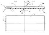
- the schematic side view and schematic top view which show the state of the emitted light from a main surface when light injects from one side end surface of the light guide which concerns on one Embodiment of this invention.
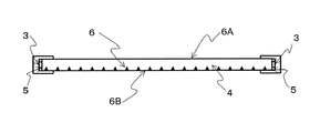
- the schematic side view and schematic top view of one Embodiment of the optical shutter or surface light source device using the light guide of this invention which made two opposing side end surfaces light incident surfaces.
- the light emission surface is constituted by each of two opposing main surfaces in the light guide according to the present invention.
- “opposing” with respect to any two surfaces of the light guide means facing each other toward the inside of the light guide.
- the light incident surface is constituted by at least one side end surface in the light guide of the present invention.
- the light incident surface may be one side end surface or each of two or more side end surfaces.
- each of the two opposing side end surfaces may be a light incident surface
- each of two orthogonal side end surfaces may be a light incident surface.
- each of the two opposing side end surfaces is a light incident surface.
- the light emitting mechanism is a mechanism for emitting light incident on the light guide of the present invention to the outside of the light guide of the present invention.
- the light emitting mechanism is formed in at least a partial region of at least one main surface of the light guide according to the present invention.
- the light emission mechanism may be formed on at least one main surface of the two main surfaces of the light guide, or may be formed on both main surfaces.
- the light emitting mechanism only needs to be formed in at least a part of the main surface, and may be formed in the entire main surface. Moreover, the light emission mechanism may be formed in a state of being divided into a plurality of regions on the main surface.
- the light emission mechanism for example, a resin in which minute concaves or convexes are formed on the surface of the main surface and a scatterer such as titanium oxide particles dispersed in an acrylic binder resin on the surface of the main surface
- a scatterer such as titanium oxide particles dispersed in an acrylic binder resin
- the depth of the recesses or the height of the protrusions is preferably 30 ⁇ m or more and 70 ⁇ m or less, and the plurality of recesses or protrusions Each part may have a variation within a range of 30 ⁇ m or more and 70 ⁇ m or less.
- the depth of the concave portion or the height of the convex portion indicates the distance from the bottom or top to the main surface (here, the flat surface portion excluding the concave or convex portion) in the cross section of the concave or convex portion.
- FIG. 1 shows a cross section 1 of a concave portion and a concave portion 2 viewed from above in a light emitting mechanism in a light guide according to an embodiment of the present invention.
- the depth of the recess is a distance Y from the bottom surface to the main surface in the recess section 1.
- the outgoing maximum angle with respect to the main surface having the light output mechanism tends to be + 60 ° or less with respect to the normal of the main surface. It is in. Further, in this case, the outgoing maximum angle with respect to the main surface having no light output mechanism tends to be + 30 ° or less with the normal of the main surface as the center.
- the output maximum angle for the main surface without the light output mechanism should be ⁇ 30 ° or more about the normal to the main surface. There is a tendency to be able to.
- the lower limit of the range of the depth of the concave portion or the height of the convex portion is more preferably 35 ⁇ m, and particularly preferably 40 ⁇ m.
- the upper limit value of the range of the depth of the concave portion or the height of the convex portion is more preferably 65 ⁇ m.
- the diameter of the recesses or protrusions is preferably 40 ⁇ m or more and 150 ⁇ m or less, and 40 ⁇ m or more per plurality of recesses or protrusions.
- the variation may be within a range of 150 ⁇ m or less.
- the diameter of the concave or convex portion indicates the maximum inner diameter of the concave or convex portion. The following description will be made using the concave portion 2 as viewed from above in FIG.
- the diameter of the concave portion is the maximum inner diameter X of the concave portion indicated by a dotted line in the concave portion 2.
- the output light efficiency of the light guide of the present invention tends to be 15% or more.
- the output light efficiency is the ratio of the sum of the light flux emitted from the light exit surface having the light exit mechanism to the light flux incident from the light entrance surface and the light flux emitted from the light exit surface not having the light exit mechanism. Indicates.
- the haze value of the light guide of the present invention tends to be 3% or less.
- the lower limit of the diameter range of the concave or convex portions is more preferably 50 ⁇ m, and particularly preferably 60 ⁇ m.
- the upper limit value of the diameter range of the concave portion or the convex portion is more preferably 130 ⁇ m, and particularly preferably 110 ⁇ m.
- the surface density of the concave or convex portions is preferably 450 dots or more and 5,000 dots or less per square inch.
- the output light efficiency of the light guide of the present invention tends to be 15% or more.
- the haze value of the light guide of the present invention tends to be 3% or less.
- the lower limit of the surface density range of the concave or convex portions is more preferably 500 dots per square inch, and particularly preferably 600 dots.
- the upper limit of the surface density range of the concave or convex portions is more preferably 4,000 dots per square inch, and particularly preferably 2,800 dots.
- the light guide of the present invention has a plate shape having two opposing main surfaces each being a light emitting surface and at least one side end surface being a light incident surface.
- the light guide of the present invention can be a plate-like body that is multilayered as necessary.
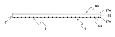
- the light guide 4 in FIG. 12 has a three-layer structure of a low refractive index resin layer 17A, a high refractive index resin layer 17B, and a low refractive index resin layer 17A. According to this, even if the surface of the light guide 4 is soiled by dust or fingerprints, it is possible to provide a feature that the soiling is not noticeable.
- FIG. 12 has a three-layer structure of a low refractive index resin layer 17A, a high refractive index resin layer 17B, and a low refractive index resin layer 17A. According to this, even if the surface of the light guide 4 is soiled by dust or fingerprints, it is possible to provide a feature that the soiling is not noticeable.
- the light guide of the present invention can be a plate-like body having a curvature as required.
- the thickness of the light guide of the present invention is, for example, 0.5 to 6 mm.
- the size of the light guide of the present invention is not limited and can be selected according to the purpose.
- the shape of the light guide of the present invention includes, for example, a square, a rectangle, a pentagon or more polygon, and a circle.
- each of the two main surfaces facing each other is a light emitting surface.
- a light emitting mechanism is formed on at least a part of the light emitting surface. The light incident from the light incident surface is emitted from the light emitting surface via the light emitting mechanism.
- the light guide of the present invention preferably has a haze value of 3% or less.
- the fog value of the light guide of the present invention By setting the fog value of the light guide of the present invention to 3% or less, when the light guide of the present invention is used for an optical shutter, the visibility on the back side when the shutter is open tends to be good.
- the haze value of the light guide of the present invention By setting the haze value of the light guide of the present invention to 3% or less, when the light guide of the present invention is used for a surface light source device such as lighting, the transparency is high when the light source is turned off, and an excellent design. There exists a tendency which can obtain the surface light source device which has property.
- the haze value of the light guide of the present invention is preferably 2.5% or less, more preferably 2% or less.
- the haze value of the light guide of the present invention is generally 0.1% or more.
- the output maximum angle is centered on the normal of the main surface (that is, the direction of the normal of the main surface is (0 °) ⁇ 60 ° or more and + 60 ° or less.
- Completely diffused light is light having a Lambertian distribution (a distribution of light having the same luminance in all directions), for example, light emitted from an LED light source without a condenser lens.
- FIG. 2 is a schematic side view showing a state of emitted light from the main surface when light is incident from one side end face of the light guide according to the embodiment of the present invention, together with a schematic top view. .
- the light 7 emitted from the LED light source 3 disposed facing the light incident surface 5 enters the light guide 4 from the light incident surface 5 and has a light emitting surface 6A and a light emitting mechanism that do not have a light emitting mechanism.
- the light is repeatedly reflected from the inner surface by the light emitting surface 6B and travels, and is emitted as emitted light 8 from the light emitting surfaces 6A and 6B by the action of the light emitting mechanism.
- the exit maximum angle is the exit angle when the luminous intensity becomes maximum as shown in FIG. 3, and as shown in FIG. 2, the direction of the light exiting from the light exit surfaces 6A and 6B and the normal of the main surface
- the normal direction is 0 °
- the light source side with respect to the normal is-
- the opposite side of the light source is +.
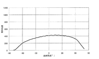
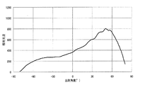
- Examples of the pattern of emitted light having an output maximum angle of ⁇ 60 ° or more and + 60 ° or less include the patterns shown in FIGS.
- the outgoing light pattern (outgoing light pattern a) shown in FIG. 3 has one main surface having a light output mechanism, and only one side end surface is a light incident surface. It is an example of the emitted light pattern from. In this example, the output maximum angle exists in the vicinity of + 10 °. When the two opposing side end surfaces are light incident surfaces, a substantially similar pattern is shown, and the exit maximum angle exists in the vicinity of the normal, for example, ⁇ 15 ° to + 15 °, particularly ⁇ 10 ° to + 10 °.
- the outgoing light pattern (outgoing light pattern b) shown in FIG. 4 has one main surface having a light emitting mechanism, and only one side end surface is a light incident surface. This is an example of the outgoing light pattern. In this example, the output maximum angle exists in the vicinity of + 50 °.
- the outgoing light pattern (outgoing light pattern c) shown in FIG. 5 has one main surface having a light output mechanism, and the main surface having the light output mechanism when two opposing side end surfaces are light incident surfaces. It is an example of the emitted light pattern from. In this example, the output maximum angle exists in the vicinity of ⁇ 50 ° and + 50 °.
- the outgoing light pattern (outgoing light pattern d) shown in FIG. 6 has two main surfaces having a light output mechanism, and the outgoing light pattern from the main surface when two opposing side end surfaces are light incident surfaces. It is an example. In this example, the output maximum angle exists from ⁇ 50 ° to + 50 °.
- the emitted light when the light source is turned on can be efficiently emitted to the front of the light emitting surface, and the back side is hardly visible. Therefore, a high shutter function, that is, a high concealment function can be exhibited.
- a light guide body in which an outgoing light pattern on one main surface is an outgoing light pattern a and an outgoing light pattern on the other main surface is an outgoing light pattern c, and outgoing light patterns on both main surfaces are It is preferable to use a light guide that is the outgoing light pattern d.
- a surface light source device in particular, a suspended illumination device, a light guide body in which the outgoing light pattern on one main surface is an outgoing light pattern a and the outgoing light pattern on the other main surface is an outgoing light pattern c is used. Is preferred.
- the light guide of the present invention preferably has an emission light efficiency of 15% or more.
- the material for the light guide of the present invention include transparent inorganic materials such as glass and transparent resin materials.
- Examples of the transparent resin used for the transparent resin material include methacrylic resin, styrene resin, polycarbonate resin, and alicyclic polyolefin resin. Among these, a methacrylic resin is preferable in terms of laser processability.
- methacrylic resin examples include homopolymers or copolymers of methacrylic acid esters.
- methacrylic acid ester examples include methyl methacrylate, ethyl methacrylate, propyl methacrylate, and cyclohexyl methacrylate.
- methacrylic acid esters acrylic acid esters such as methyl acrylate, ethyl acrylate and n-butyl acrylate, ⁇ , ⁇ -ethylenically unsaturated carboxylic acids such as acrylic acid, methacrylic acid and maleic anhydride, styrene, etc.
- Other vinyl monomers such as aromatic vinyl monomers and vinyl cyanide monomers such as acrylonitrile may be copolymerized.
- a methyl methacrylate homopolymer or a copolymer containing methyl methacrylate as a main component is preferable in terms of processability and low cost.
- the scatterer can be dispersed inside the light guide as required.
- Examples of the scatterer include inorganic diffusing agents and organic diffusing agents.
- Examples of the inorganic diffusing agent include glass fine particles and silica fine particles.
- organic diffusing agent examples include silicone fine particles and styrene fine particles.
- the light guide of the present invention can be manufactured, for example, by forming a light emitting mechanism on the main surface of a plate-shaped light guide material, that is, a light guide base plate (light guide blank).
- Examples of the method for forming the concave portion as the light emitting mechanism include a laser processing method and a machining method using a blade.
- Examples of the method for forming the convex portion as the light emitting mechanism include a hot press method, an injection molding method, a screen printing method, and an ink jet printing method.
- a scatterer When forming a convex part by printing methods, such as a screen printing method and an inkjet printing method, as a light emission mechanism, a scatterer can be contained in the ink used in order to form a convex part.
- a method of forming the light emitting mechanism on the main surface of the light guide body base plate a method of forming a recess by a laser processing method is preferable from the viewpoint of workability and mass productivity.
- Examples of the method of forming the recess by the laser processing method include a method of irradiating the main surface of the light guide base plate with laser light.
- the laser those having good processing efficiency with respect to the light guide base plate are preferable, and examples thereof include an infrared laser such as a carbon dioxide laser (CO 2 laser).
- CO 2 laser carbon dioxide laser
- a laser having a wavelength of 9.3 ⁇ m or 10.6 ⁇ m is preferable. By using a laser having this wavelength, the methacrylic resin sheet absorbs laser light and is heated, so that laser processing can be performed efficiently.
- Examples of the carbon dioxide laser processing apparatus include a CO 2 gas laser processing machine PLS4.75 (trade name, wavelength: 10.6 ⁇ m, average output: 40 W) manufactured by Universal Laser Co., Ltd.
- the shape (diameter and depth) of the recesses can be controlled by changing irradiation conditions such as laser output, scanning speed, focal position (focus position), and numerical aperture of the condenser lens. Since the laser is radiated in a pulse shape, a plurality of concave portions spaced apart from each other are formed with scanning.
- a light source is arranged to face the light incident surface of the light guide of the present invention.
- the light source include an LED and a cold cathode fluorescent lamp.
- the LED is preferable from the viewpoint that power consumption can be reduced and the drive circuit can be simplified.
- a white LED may be used, a colored LED may be used according to the application, or LEDs of different colors may be combined. Further, as the LED, an LED without a lens (an LED that emits completely diffused light) may be used, or an LED with a lens may be used as long as it does not emit parallel light.
- the above-described LEDs can be used in combination depending on the purpose.
- LED light source When an LED light source is used as the light source of the optical shutter or the surface light source device of the present invention, one or a plurality of LED light sources can be arranged facing one side end surface.
- the light guide used in the optical shutter and the surface light source device of the present invention may have at least one light incident surface. When there are two light incident surfaces, the two opposite side end surfaces are used as the light incident surfaces. It is preferable.
- the light guide used in the optical shutter or the surface light source device of the present invention may have a light emission mechanism formed on one main surface, or a light emission mechanism formed on both main surfaces.
- FIG. 7 is a schematic side view of an optical shutter or a surface light source device using a light guide body 4 in which each of two opposing side end surfaces is a light incident surface 5 and a concave portion is formed as a light emitting mechanism 6 on one main surface.
- FIG. 7 is a schematic side view of an optical shutter or a surface light source device using a light guide body 4 in which each of two opposing side end surfaces is a light incident surface 5 and a concave portion is formed as a light emitting mechanism 6 on one main surface.
- the light emitted from the light source 3 enters the light guide 4 from the light incident surface 5 and is emitted from the emission surface 6A having no light emission mechanism and the emission surface 6B having the light emission mechanism 6. At this time, since the light emitted from the emission surface 6A that does not have the light emission mechanism is light reflected by the light emission mechanism 6, the emission light pattern is the aforementioned emission light pattern a.
- the emission light pattern is the aforementioned emission light pattern c.
- an optical shutter or a surface light source device using a light guide body in which a concave portion is formed as a light emitting mechanism on both main surfaces and each of two opposing side end surfaces being light incident surfaces will be described with reference to FIG. explain.
- the light emitted from the light source 3 enters the light guide 4 from the light incident surface 5 and is emitted from an emission surface 6B having two light emission mechanisms 6 facing each other.
- the outgoing light pattern of the light emitted from the outgoing surface 6B having the light outgoing mechanism 6 has the outgoing light pattern a and the outgoing light pattern c because the light outgoing mechanism 6 is formed on both main surfaces.
- the above-described outgoing light pattern d is obtained.
- the optical shutter of the present invention is in a shutter open state when the light source is turned off, and is in a closed state when the light source is turned on.
- the optical shutter according to the present invention uses the light guide according to the present invention, when the shutter is open, the front side of the optical shutter can be seen well, and when the shutter is closed, a high concealing function is provided. Can be expressed.
- the high concealment function refers to a function that provides high concealment as a shutter and makes the back side invisible, when viewed from the front or obliquely of the optical shutter.
- an outgoing light pattern on one main surface is an outgoing light pattern a
- an outgoing light pattern on the other main surface is an outgoing light pattern c.
- a light guide that is the light emission pattern d in terms of high concealment function.
- the surface light source device of the present invention uses the light guide of the present invention, it can be used as an illuminating device that is highly transparent when the light source is turned off and has excellent design.
- a light guide having a main surface that emits the light of the emitted light pattern c is used and the main surface is installed so as to face the ceiling.
- indirect light it is preferable in that indirect light can be used efficiently.
- part means “part by mass”.
- the diameter of a recessed part is the largest internal diameter X on the basis of the upper surface of a light-guide test piece, as shown in FIG.
- the depth of a recessed part is the distance Y to the deepest location of a recessed part on the basis of the upper surface of a light-guide test piece, as shown in FIG.
- (B) Area density of recess
- the area density of the recess of the light guide specimen was measured by the following method using a laser microscope (OLS-3500 (trade name) manufactured by Olympus Corporation). First, after selecting an objective lens ( ⁇ 10) and obtaining data of a two-dimensional image of a main surface (length 10.24 mm ⁇ width 10.24 mm) having a light emitting mechanism of a light guide specimen, 1 square inch The number of hit recesses was determined to obtain the surface density of the recesses.
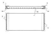
- (D) Output maximum angle The output maximum angle was measured by the following method. As shown in FIG. 9, the LED light source 3 (Nichia Corporation (Nichia Corporation)) is formed on one side end surface of the optical shutter test piece 15 with the main surface opposite to the main surface of the light emitting mechanism formed facing the luminance meter 9. Product name: NS2W123B) is attached, and the upper main surface is shielded by a shading cover 16 having a circular opening with a diameter of 10 mm in the center, and then a luminance meter 9 ((stock) ) Topcon's BM-7 (trade name)) is installed above the optical shutter test piece 15, centering on the center of the upper main surface of the optical shutter test piece 15 and from the luminance meter 9 to the upper main surface.
- a luminance meter 9 ((stock) ) Topcon's BM-7 (trade name)
- the light-shielding cover 16 was installed, and the luminance meter was made to function as a photometer by increasing the measurement angle of the luminance meter 9 (2 °).
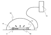
- (E) Output light efficiency The output light efficiency was measured by the method shown below. As shown in FIG. 10, the LED light source 3 (manufactured by Nichia Corporation, product name: NS2W123B) is attached to one side end surface of the light guide test piece 10, and a surface other than the upper surface of the main surface is covered with a light-shielding cover. 11 after being shielded from light, installed in a half moon integrating sphere 12 (Otsuka Electronics Co., Ltd., trade name: HM-1030), applying a current of 60 mA to the LED light source 3 to test a light flux of 13.5 lm It was made to inject into the piece 10.
- a half moon integrating sphere 12 (Otsuka Electronics Co., Ltd., trade name: HM-1030)
- the main surface having the light emission mechanism of the light guide body test piece 10 and the main surface not having the light emission mechanism are arranged as upper surfaces, respectively, and emission of the main surface of the light guide body test piece 10 having the light emission mechanism is performed.
- the light beam Ia and the outgoing light beam Ib on the main surface not having the light emitting mechanism were measured using a light beam detector 13 (trade name: MCPD-9800, manufactured by Otsuka Electronics Co., Ltd.) connected to a half moon integrating sphere, The output light efficiency was obtained by the following formula.
- Output light efficiency (%) ( ⁇ Outgoing light beam Ia (lm) + Outgoing light beam Ib (lm) ⁇ / Incoming light beam (13.5 (lm)) * 100
- (B) Concealment A (Concealment function when viewed from an angle)
- the material was placed at a position 20 cm away from the back side of the main surface that does not have the light emitting mechanism of the light guide of the optical shutter.
- the visibility of the document is confirmed with the light source of the optical shutter turned on at an angle of 45 ° from a position 20 cm away from the front side of the main surface having the light emitting mechanism of the light guide of the optical shutter.
- the concealment function when viewed from the oblique side of the shutter was evaluated according to the following criteria. ⁇ : It is difficult to see the characters of the material, and the concealment function is good.
- X It is easy to visually recognize the characters of the material, and the concealment function is poor.
- (C) Concealment B (Concealment function when viewed from the front)
- the material was placed at a position 20 cm away from the back side of the main surface that does not have the light emitting mechanism of the light guide of the optical shutter.
- the visibility of the material is confirmed with the light source of the optical shutter turned on from the position 20 cm away from the front side of the main surface having the light emission mechanism of the light guide of the optical shutter in the normal direction of the emission surface.
- the shutter function when viewed from the normal direction of the exit surface of the shutter was evaluated according to the following criteria. ⁇ : It is difficult to see the characters of the material, and the concealment function is good.
- X It is easy to visually recognize the characters of the material, and the concealment function is poor.
- the reaction vessel was cooled to room temperature to obtain a syrup having a polymer content of 26% by mass, a mass average molecular weight of 116,000, and an absolute viscosity of 1.8 Pa ⁇ s at 20 ° C.
- a syrup having a polymer content of 26% by mass, a mass average molecular weight of 116,000, and an absolute viscosity of 1.8 Pa ⁇ s at 20 ° C.
- 0.35 part of t-hexyl peroxypivalate manufactured by NOF Corporation, perhexyl PV (trade name)
- 0.13 part of n-dodecyl mercaptan as a molecular weight regulator were added and stirred.
- a thermopolymerizable viscous liquid was prepared.
- thermopolymerizable viscous liquid is poured into a mold formed by sandwiching two tempered glass plates facing each other through a polyvinyl chloride gasket at a distance of 2.3 mm, and heated in 80 ° C. warm water for 45 minutes. After being immersed and polymerized, it was heat-treated in an air heating furnace at 135 ° C. for 60 minutes. After completion of the heat treatment, the substrate was cooled at room temperature, and the gasket and the tempered glass plate were removed to obtain a light guide plate ( ⁇ ) having a plate thickness of 3 mm.
- Example 1 From the light guide base plate ( ⁇ ) obtained in Production Example 1, using a panel saw (SZ-III (trade name) manufactured by Shinx Co., Ltd.), a base plate for optical shutter of 210 mm ⁇ 300 mm and 60 mm ⁇ 60 mm The light guide body test piece base plate was cut out.
- SZ-III trade name manufactured by Shinx Co., Ltd.
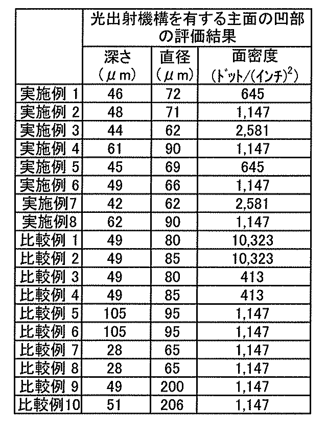
- the depth of the recess was 46 ⁇ m, the diameter of the recess was 72 ⁇ m, and the surface density of the recess was 645 dots / (inch) 2 .
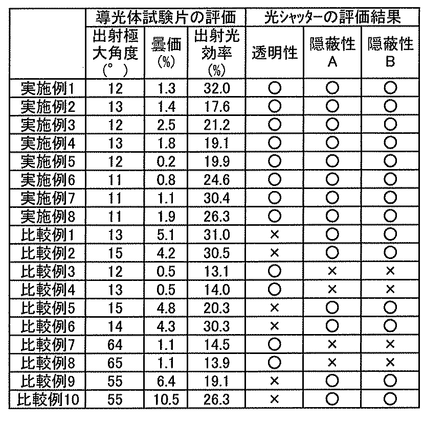
- the results are shown in Table 2.
- LED light sources 3 manufactured by Nichia Corporation, product name: NS2W123B
- NS2W123B product name: NS2W123B
- the obtained optical shutter has good transparency when the shutter is open (when the LED light source is turned off), and also has concealability when the shutter is closed (when the LED light source is turned on). Both B (the hiding function seen from the front) were also good. The results are shown in Table 3.
- Table 1 The abbreviations in Table 1 indicate the following.
- HPPDF Condensing lens (trade name, manufactured by Universal Laser Co., Ltd.) 1.5 in: Condensing lens (trade name, manufactured by Universal Laser Co., Ltd.)
- Example 2 to 8 An optical shutter test piece, a light guide specimen and an optical shutter were obtained in the same manner as in Example 1 except that the light guide base plate and the laser processing conditions were changed as shown in Table 1. The evaluation results are shown in Tables 2 and 3.
- Comparative Example 1 the surface density of the recesses was 10,323 dots / (inch) 2 , the haze value was as high as 5.1%, and the transparency of the optical shutter was poor.
- Comparative Example 2 the surface density of the recesses was 10,323 dots / (inch) 2 , the haze value was as high as 4.2%, and the transparency of the optical shutter was poor.
- Comparative Example 3 since the surface density of the recesses was as small as 413 dots / (inch) 2 , the output light efficiency was as low as 13.1%, and the concealability (A) and concealability (B) were poor.
- Comparative Example 4 since the surface density of the recesses was as small as 413 dots / (inch) 2 , the output light efficiency was as low as 14.0%, and the concealability (A) and concealability (B) were poor.
- the depth of the concave portion was as deep as 105 ⁇ m and the haze value was as high as 4.8%, so the transparency of the optical shutter was poor.
- the depth of the concave portion was as deep as 105 ⁇ m and the haze value was as high as 4.3%, so the transparency of the optical shutter was poor.
- Comparative Example 7 since the depth of the concave portion is as shallow as 28 ⁇ m, the output light efficiency is as low as 14.5%, the maximum output maximum angle is as large as 64 °, and the concealability (A) and concealability (B) are poor. It was. In Comparative Example 8, since the depth of the concave portion is as shallow as 28 ⁇ m, the output light efficiency is as low as 13.9%, the maximum angle of the output is as large as 65 °, and the concealability (A) and concealability (B) are poor. It was.
- Example 1 except that a CO 2 laser marker (manufactured by Keyence Co., Ltd., ML-Z9525 (trade name)) is used instead of the CO 2 laser processing machine with a condenser lens, and the laser processing conditions shown in Table 4 are used. In the same manner, a test piece for optical shutter and a test piece for light guide were obtained. The evaluation results are shown in Tables 2 and 3.
- a CO 2 laser marker manufactured by Keyence Co., Ltd., ML-Z9525 (trade name)
- Table 4 the laser processing conditions shown in Table 4
- Comparative Example 9 since the diameter of the recess was as large as 200 ⁇ m, the haze was as high as 6.4%, and the transparency of the optical shutter was poor. In Comparative Example 10, since the diameter of the recess was as large as 206 ⁇ m, the haze value was as high as 10.5%, and the transparency of the optical shutter was poor.
- the light guide of the present invention can be used for an optical shutter, and is suitable for use in architectural windows such as partitions and skylights.
- the light guide of the present invention can be used for a surface light source device and is suitable for use in an illumination device such as a ceiling light.
Landscapes
- Physics & Mathematics (AREA)
- General Physics & Mathematics (AREA)
- Optics & Photonics (AREA)
- Engineering & Computer Science (AREA)
- Manufacturing & Machinery (AREA)
- Planar Illumination Modules (AREA)
- Light Guides In General And Applications Therefor (AREA)
- Arrangement Of Elements, Cooling, Sealing, Or The Like Of Lighting Devices (AREA)
- Non-Portable Lighting Devices Or Systems Thereof (AREA)
- Microelectronics & Electronic Packaging (AREA)
Abstract
Description
[1] 対向する2つの主面が光出射面であり、少なくとも1つの側端面が光入射面である板状の導光体であって、少なくとも一方の主面の少なくとも一部の領域に光出射機構が形成されており、光出射機構が形成された領域における曇価が3%以下で、少なくとも1つの光入射面から完全拡散光が入射されたときに、主面の光出射機構が形成された領域からの出射光の光度が極大となる角度(以下、「出射極大角度」という)が、主面の法線を中心に-60°以上+60°以下の範囲内にあり、出射光効率が15%以上である導光体。
[2] 少なくとも1つの光入射面から完全拡散光が入射されたときに、一方の主面の出射極大角度が、主面の法線を中心に-30°以上+30°以下の範囲内にあり、もう一方の主面の出射極大角度が、-60°以上-30°以下の範囲内、+30°以上+60°以下の範囲内、及び-60°以上-30°以下と+30°以上+60°以下との範囲内から選ばれる少なくとも1種の範囲内にある[1]に記載の導光体。
[3] 対向する2つの主面が光出射面であり、少なくとも1つの側端面が光入射面である板状の導光体であって、少なくとも一方の主面の少なくとも一部の領域に光出射機構として微小な凹部又は凸部が形成されており、凹部の深さ又は凸部の高さが30μm以上70μm以下で、凹部又は凸部の直径が40μm以上150μm以下で、凹部又は凸部の面密度が1平方インチ当たり450ドット以上5,000ドット以下である導光体。ここで、「ドット」は個数単位であり、1ドットは1個であることを示す。
[4] 導光体元板の少なくとも一方の主面の少なくとも一部の領域にレーザー光を照射して、光出射機構を形成する[1]~[3]のいずれかに記載の導光体の製造方法。
[5] [1]~[3]のいずれかに記載の導光体の光入射面に対向して光源が配置されている光シャッター。
[6] [1]~[3]のいずれかに記載の導光体の光入射面に対向して光源が配置されている面光源装置。
光出射面は、本発明の導光体における対向する2つの主面のそれぞれにより構成される。
尚、本明細書において、導光体の何れか2つの面につき「対向する」とは、導光体内側 に向けて互いに向き合うことを意味する。
光入射面は、本発明の導光体における少なくとも1つの側端面により構成される。
光入射面は、1つの側端面でもよく、2つ以上の複数の側端面のそれぞれでもよい。
光入射面が2つある場合は、対向する2つの側端面のそれぞれが光入射面でもよく、直交する2つの側端面のそれぞれが光入射面でもよい。光出射面から出射する光の均一性の面から、例えば図7に示すように、対向する2つの側端面のそれぞれが光入射面であることが好ましい。
光出射機構は、本発明の導光体に入射された光を本発明の導光体の外部に出射させるための機構である。
本発明の導光体は、それぞれが光出射面である対向する2つの主面及び少なくとも1つが光入射面である側端面を有し、板状である。
本発明の導光体は、例えば図12に示すように、必要に応じて多層化した板状体とすることができる。図12の導光体4は、低屈折率樹脂層17A、高屈折率樹脂層17B及び低屈折率樹脂層17Aの3層構造とされている。これによれば、導光体4の表面がほこりや指紋により汚れても、その汚れが目立ちにくいという特長を付与することができる。
図12において、光入射面5、並びに、光出射機構を有さない光出射面6A及び光出射機構6を有する光出射面6Bが、示されている。
本発明の導光体は、必要に応じて曲率を持たせた板状体とすることができる。
本発明の光シャッター及び面光源装置は、本発明の導光体の光入射面に対向して光源が配置されているものである。
光源としては、例えば、LED及び冷陰極管蛍光灯が挙げられる。これらの中で、消費電力を少なくできる点や駆動回路を簡略化できる点から、LEDが好ましい。
(a)凹部の深さ及び直径
レーザー顕微鏡(オリンパス(株)製、OLS-3500(商品名))を用いて導光体試験片の凹部の深さ及び直径を以下の方法で測定した。
まず、導光体試験片の中央部分の任意の凹部を一つ選び、対物レンズ(×50)を用いて凹部の深さ方向の測定ピッチを0.25μmに設定し、レーザー強度レベルを100に設定して凹部の3次元画像のデータを得た。
次いで、得られた3次元画像のデータに対して、レーザー顕微鏡に内蔵されている凹凸形状用ノイズ除去処理操作を一回行って、暗ノイズを除去し、レーザー顕微鏡に内蔵されている段差計測操作により上記の凹部の深さ及び直径を測定した。
尚、凹部の直径は、図1に示すように、導光体試験片の上面を基準とした最大内径Xである。また、凹部の深さは、図1に示すように、導光体試験片の上面を基準とした凹部の最も深い箇所までの距離Yである。
レーザー顕微鏡(オリンパス(株)製、OLS-3500(商品名))を用いて導光体試験片の凹部の面密度を以下の方法で測定した。
まず、対物レンズ(×10)を選択して導光体試験片の光出射機構を有する主面(縦10.24mm×横10.24mm)の2次元画像のデータを得た後、1平方インチ当たりの凹部の個数を求め、凹部の面密度を得た。
HAZEMETER((株)村上色彩技術研究所製、HM―150(商品名))の受光側に導光体試験片の光出射機構を有する主面をセットし、JIS K 7136に準拠して曇価を測定した。
出射極大角度は、以下に示す方法により測定した。
図9に示すように、光出射機構形成主面の反対側の主面を輝度計9に向けて上側にした光シャッター用試験片15の1つの側端面にLED光源3(日亜化学工業(株)製、商品名:NS2W123B)を取り付け、上側主面を中央部に直径10mmの円形の開口部をもつ遮光カバー16で遮光した後、測定角を2°に設定した輝度計9((株)トプコン製、BM-7(商品名))を光シャッター用試験片15の上方に設置し、光シャッター用試験片15の上側主面の中央部を中心に、輝度計9から上側主面の中央部までの距離が一定の距離(Z=650mm)となるような条件で図示される方向に1°刻みで輝度計9を移動させて相対光度を測定し、出射極大角度を求めた。なお、遮光カバー16を設置し、輝度計9の測定角を大きくする(2°)ことで、輝度計を光度計として機能させた。
出射光効率は、以下に示す方法により測定した。
図10に示すように、導光体試験片10の1つの側端面にLED光源3(日亜化学工業(株)製、商品名:NS2W123B)を取り付け、主面の上面以外の面を遮光カバー11で遮光した後、ハーフムーン積分球12(大塚電子(株)、商品名:HM-1030)内に設置し、LED光源3に電流60mAを印加して13.5lmの光束を導光体試験片10に入射させるようにした。ここで、導光体試験片10の光出射機構を有する主面及び光出射機構を有さない主面をそれぞれ上面として配置し、導光体試験片10の光出射機構を有する主面の出射光束Ia及び光出射機構を有さない主面の出射光束Ibをそれぞれハーフムーン積分球に接続した光束検出器13(大塚電子(株)製、商品名:MCPD-9800)を用いて測定し、下式により出射光効率を求めた。
出射光効率(%)=({出射光束Ia(lm)+出射光束Ib(lm)}/入射光束(13.5(lm))*100
(a)透明性
光シャッターの導光体の光出射機構を有さない主面の後ろ側の20cm離れた位置に資料を配置した。次いで、光シャッターの導光体の光出射機構を有する主面の手前側の20cm離れた位置から、光シャッターの光源を消灯した状態で資料の視認性を確認し、光シャッターの導光体の透明性を以下の基準で評価した。
○:資料の文字を視認し易く、光源消灯時の透明性が良好である。
×:資料の文字を視認し難く、光源消灯時の透明性が不良である。
(b)隠蔽性A(斜めから見たときの隠蔽機能)
光シャッターの導光体の光出射機構を有さない主面の後ろ側の20cm離れた位置に資料を配置した。次いで、光シャッターの導光体の光出射機構を有する主面の手前側の20cm離れた位置から斜め45°の角度で、光シャッターの光源を点灯した状態で資料の視認性を確認し、光シャッターの斜めから見たときの隠蔽機能を以下の基準で評価した。
○:資料の文字を視認し難く、隠蔽機能が良好である。
×:資料の文字を視認し易く、隠蔽機能が不良である。
(c)隠蔽性B(正面から見たときの隠蔽機能)
光シャッターの導光体の光出射機構を有さない主面の後ろ側の20cm離れた位置に資料を配置した。次いで、光シャッターの導光体の光出射機構を有する主面の手前側の20cm離れた位置から出射面法線方向に、光シャッターの光源を点灯した状態で資料の視認性を確認し、光シャッターの出射面法線方向から見たときのシャッター機能を以下の基準で評価した。
○:資料の文字を視認し難く、隠蔽機能が良好である。
×:資料の文字を視認し易く、隠蔽機能が不良である。
冷却管、温度計及び攪拌機を備えた反応器に、メタクリル酸メチル98部、アクリル酸n-ブチル2部、分子量調整剤としてn-ドデシルメルカプタン0.063部及び離型剤としてジオクチルスルホ琥珀酸ナトリウム0.005部を供給した。
反応器内を攪拌しながら重合開始剤として2、2’-アゾビス-(2、4-ジメチルバレロニトリル)0.10部を添加した後に内温90℃まで昇温し、10分間保持した。次いで、反応容器を室温まで冷却して、重合体含有率26質量%、質量平均分子量11.6万、20℃における絶対粘度1.8Pa・sのシラップを得た。
このシラップ100部にt-ヘキシルパーオキシピバレート(日油(株)製、パーヘキシルPV(商品名))0.35部及び分子量調整剤としてn-ドデシルメルカプタン0.13部を添加した後に攪拌し、熱重合性粘性液体を調製した。
この熱重合性粘性液体を、ポリ塩化ビニル製ガスケットを介して2.3mmの間隔で相対する2枚の強化ガラス板で挟むことにより形成された鋳型に注入し、80℃の温水中に45分間浸漬して重合させた後、135℃の空気加熱炉中で60分間熱処理した。熱処理終了後、室温下で冷却し、ガスケット及び強化ガラス板を取り除くことにより板厚3mmの導光体元板(α)を得た。
成形材料用透明メタクリル樹脂(三菱レイヨン(株)製、アクリペットVH6#001(商品名))を65mmφベント付一軸押出機で溶融混練し、Tダイから樹脂温度260℃にて溶融押出しして、表面が平滑な、下ローラー、中ローラー及び上ローラーの組み合わせからなる3本ローラーを用いて、下ローラーの表面温度90℃、中ローラーの表面温度175℃及び上ローラーの表面温度120℃に設定してプレス成形し、厚さ3mmの導光体元板(β)を得た。
製造例1で得られた導光体元板(α)から、パネルソー(シンクス(株)製、SZ―III(商品名))を用いて、210mm×300mmの光シャッター用元板と60mm×60mmの導光体試験片用元板とを切出した。

HPDFO:集光レンズ(ユニバーサルレーザー(株)製、商品名)
1.5in:集光レンズ(ユニバーサルレーザー(株)製、商品名)
導光体元板及びレーザー加工条件を表1のように変更する以外は実施例1と同様にして
光シャッター用試験片、導光体試験片及び光シャッターを得た。評価結果を表2及び表3に示す。
導光板元板及びレーザー加工条件を表1のように変更する以外は実施例1と同様にして光シャッター用試験片、導光体試験片及び光シャッターを得た。評価結果を表2及び表3に示す。
比較例2では、凹部の面密度が10,323ドット/(インチ)2で、曇価が4.2%と高く、光シャターの透明性が不良であった。
比較例3では、凹部の面密度が413ドット/(インチ)2と小さいため出射光効率が13.1%と低く、隠蔽性(A)及び隠蔽性(B)が不良であった。
比較例4では、凹部の面密度が413ドット/(インチ)2と小さいため出射光効率が14.0%と低く、隠蔽性(A)及び隠蔽性(B)が不良であった。
比較例5では、凹部の深さが105μmと深く、曇価が4.8%と高いため光シャターの透明性が不良であった。
比較例6では、凹部の深さが105μmと深く、曇価が4.3%と高いため光シャターの透明性が不良であった。
比較例7では、凹部の深さが28μmと浅いため出射光効率が14.5%と低く、更に出射極大角度が64°と大きく、隠蔽性(A)及び隠蔽性(B)が不良であった。
比較例8では、凹部の深さが28μmと浅いため出射光効率が13.9%と低く、更に出射極大角度が65°と大きく、隠蔽性(A)及び隠蔽性(B)が不良であった。
集光レンズを取り付けたCO2レーザー加工機の代わりにCO2レーザーマーカー((株)キーエンス製、ML―Z9525(商品名))を用い、表4に示すレーザー加工条件とする以外は実施例1と同様にして光シャッター用試験片と導光体試験片を得た。評価結果を表2及び表3に示す。
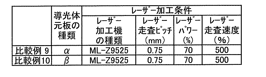
比較例10では、凹部の直径は206μmと大きいため曇価が10.5%と高く、光シャターの透明性が不良であった。
2:上から見た凹部
3:LED光源
4:導光体
5:光入射面
6:光出射機構
6A:光出射機構を有さない光出射面
6B:光出射機構を有する光出射面
7:LED光源より出射した光
8:光出射面より出射する光
9:輝度計
10:導光体試験片
11:遮光カバー
12:ハーフムーン積分球
13:光束検出器
14:カバー
15:光シャッター用試験片
16:遮光カバー
17A:低屈折率樹脂層
17B:高屈折率樹脂層
Claims (6)
- 対向する2つの主面が光出射面であり、少なくとも1つの側端面が光入射面である板状の導光体であって、少なくとも一方の主面の少なくとも一部の領域に光出射機構が形成されており、光出射機構が形成された領域における曇価が3%以下で、少なくとも1つの光入射面から完全拡散光が入射されたときに、主面の光出射機構が形成された領域からの出射光の光度が極大となる角度が、主面の法線を中心に-60°以上+60°以下の範囲内にあり、出射光効率が15%以上である導光体。
- 少なくとも1つの光入射面から完全拡散光が入射されたときに、一方の主面の光出射機構が形成された領域からの出射光の光度が極大となる角度が、主面の法線を中心に-30°以上+30°以下の範囲内にあり、もう一方の主面の光出射機構が形成された領域からの出射光の光度が極大となる角度が、-60°以上-30°以下の範囲内、+30°以上+60°以下の範囲内、及び-60°以上-30°以下と+30°以上+60°以下との範囲内から選ばれる少なくとも1種の範囲内にある請求項1に記載の導光体。
- 対向する2つの主面が光出射面であり、少なくとも1つの側端面が光入射面である板状の導光体であって、少なくとも一方の主面の少なくとも一部の領域に光出射機構として微小な凹部又は凸部が形成されており、凹部の深さ又は凸部の高さが30μm以上70μm以下で、凹部又は凸部の直径が40μm以上150μm以下で、凹部又は凸部の面密度が1平方インチ当たり450ドット以上5,000ドット以下である導光体。
- 導光体元板の少なくとも一方の主面の少なくとも一部の領域にレーザー光を照射して、光出射機構を形成する請求項1~3のいずれかに記載の導光体の製造方法。
- 請求項1~3のいずれかに記載の導光体の光入射面に対向して光源が配置されている光シャッター。
- 請求項1~3のいずれかに記載の導光体の光入射面に対向して光源が配置されている面光源装置。
Priority Applications (4)
| Application Number | Priority Date | Filing Date | Title |
|---|---|---|---|
| US14/437,499 US9507072B2 (en) | 2012-10-26 | 2013-10-23 | Light guide, manufacturing method of light guide, optical shutter, and planar light-source device |
| CN201380056130.0A CN104769351A (zh) | 2012-10-26 | 2013-10-23 | 导光体、导光体的制造方法、光学快门以及面光源装置 |
| KR1020157009461A KR101775802B1 (ko) | 2012-10-26 | 2013-10-23 | 도광체, 도광체의 제조 방법, 광셔터 및 면광원 장치 |
| JP2013549661A JP6424428B2 (ja) | 2012-10-26 | 2013-10-23 | 導光体、導光体の製造方法、光シャッター及び面光源装置 |
Applications Claiming Priority (2)
| Application Number | Priority Date | Filing Date | Title |
|---|---|---|---|
| JP2012-236360 | 2012-10-26 | ||
| JP2012236360 | 2012-10-26 |
Publications (1)
| Publication Number | Publication Date |
|---|---|
| WO2014065304A1 true WO2014065304A1 (ja) | 2014-05-01 |
Family
ID=50544681
Family Applications (1)
| Application Number | Title | Priority Date | Filing Date |
|---|---|---|---|
| PCT/JP2013/078649 Ceased WO2014065304A1 (ja) | 2012-10-26 | 2013-10-23 | 導光体、導光体の製造方法、光シャッター及び面光源装置 |
Country Status (6)
| Country | Link |
|---|---|
| US (1) | US9507072B2 (ja) |
| JP (1) | JP6424428B2 (ja) |
| KR (1) | KR101775802B1 (ja) |
| CN (1) | CN104769351A (ja) |
| TW (1) | TWI601989B (ja) |
| WO (1) | WO2014065304A1 (ja) |
Cited By (1)
| Publication number | Priority date | Publication date | Assignee | Title |
|---|---|---|---|---|
| WO2019225636A1 (ja) | 2018-05-22 | 2019-11-28 | 三菱ケミカル株式会社 | カラー表示装置、車両内外装部材、照明灯用ランプ、表示用看板及び車両 |
Families Citing this family (6)
| Publication number | Priority date | Publication date | Assignee | Title |
|---|---|---|---|---|
| JP6430291B2 (ja) * | 2014-07-28 | 2018-11-28 | 日立アプライアンス株式会社 | 照明装置 |
| KR102397362B1 (ko) * | 2015-05-28 | 2022-05-20 | 엘지이노텍 주식회사 | 조명장치 및 이를 포함하는 차량용램프 |
| CN109477626A (zh) * | 2016-06-10 | 2019-03-15 | 康宁股份有限公司 | 包含光提取特征的玻璃制品 |
| CN110906272B (zh) * | 2018-09-14 | 2021-11-16 | 深圳市绎立锐光科技开发有限公司 | 一种光源装置及车灯 |
| DE102021001512B4 (de) * | 2021-03-23 | 2023-03-16 | Mercedes-Benz Group AG | Zierteil mit einem Flächenlichtleiter |
| US11149922B1 (en) | 2021-04-16 | 2021-10-19 | Eduardo Reyes | Light output reducing shutter system |
Citations (8)
| Publication number | Priority date | Publication date | Assignee | Title |
|---|---|---|---|---|
| JP2004046076A (ja) * | 2002-03-15 | 2004-02-12 | Mitsubishi Rayon Co Ltd | 光偏向素子及び面光源装置 |
| JP2007059164A (ja) * | 2005-08-23 | 2007-03-08 | Fujifilm Corp | 導光板、これを用いる面状照明装置および液晶表示装置 |
| JP2008112611A (ja) * | 2006-10-30 | 2008-05-15 | Jikco Ltd | プリズムシート、照明装置及び発光標識システム |
| JP2009300989A (ja) * | 2008-05-15 | 2009-12-24 | Mitsubishi Rayon Co Ltd | 光偏向シートおよびそれを備えた面光源装置 |
| JP2010085425A (ja) * | 2008-09-29 | 2010-04-15 | Mitsubishi Rayon Co Ltd | レンズシート、面光源装置及び液晶表示装置 |
| JP2010262742A (ja) * | 2009-04-30 | 2010-11-18 | Kowa Co | Led照明装置 |
| JP2011527818A (ja) * | 2008-07-10 | 2011-11-04 | スリーエム イノベイティブ プロパティズ カンパニー | 粘弾性導光材 |
| JP2012079474A (ja) * | 2010-09-30 | 2012-04-19 | Kuraray Co Ltd | 発光体 |
Family Cites Families (19)
| Publication number | Priority date | Publication date | Assignee | Title |
|---|---|---|---|---|
| US5613751A (en) * | 1995-06-27 | 1997-03-25 | Lumitex, Inc. | Light emitting panel assemblies |
| US6500603B1 (en) * | 1999-11-11 | 2002-12-31 | Mitsui Chemicals, Inc. | Method for manufacturing polymer optical waveguide |
| JP2002023155A (ja) * | 2000-07-05 | 2002-01-23 | Nitto Denko Corp | 反射型液晶表示装置 |
| TW574509B (en) * | 2001-02-14 | 2004-02-01 | Yuka Denshi Co Ltd | Light guide body, light reflective sheet and surface light source device and liquid crystal device using the light reflective sheet, and the manufacturing method of light reflective sheet |
| JP2003046076A (ja) * | 2001-07-27 | 2003-02-14 | Toshiba Corp | シミュレーションシステムおよびシミュレーション方法 |
| JP3882108B2 (ja) * | 2001-11-14 | 2007-02-14 | 株式会社Inax | 光シャッター及びこれを用いた収納家具 |
| CN100470330C (zh) * | 2002-01-18 | 2009-03-18 | 三菱丽阳株式会社 | 光源装置 |
| JP4256716B2 (ja) * | 2003-05-12 | 2009-04-22 | アルプス電気株式会社 | 光源ユニット、照明装置および液晶表示装置 |
| EP2277081A2 (en) * | 2008-05-08 | 2011-01-26 | Koninklijke Philips Electronics N.V. | Lighting device |
| JP2010103068A (ja) | 2008-10-27 | 2010-05-06 | Kuroda Denki Kk | 導光板の製造方法、導光板及び光源装置 |
| JP2010157475A (ja) * | 2009-01-05 | 2010-07-15 | Sony Corp | 照明装置および表示装置 |
| WO2010113422A1 (ja) * | 2009-03-31 | 2010-10-07 | 株式会社クラレ | 発光体 |
| RU2012127562A (ru) * | 2009-12-03 | 2014-01-10 | Конинклейке Филипс Электроникс Н.В. | Прозрачный излучающий оконный элемент |
| WO2011093173A1 (ja) * | 2010-01-29 | 2011-08-04 | 日本ゼオン株式会社 | 導光体、照明装置及び液晶表示装置 |
| JP2012124064A (ja) * | 2010-12-09 | 2012-06-28 | Sumitomo Chemical Co Ltd | 導光板、面光源装置及び透過型画像表示装置 |
| JP2012156092A (ja) * | 2011-01-28 | 2012-08-16 | Fujifilm Corp | 面状照明装置 |
| SG195039A1 (en) * | 2011-05-20 | 2013-12-30 | 3M Innovative Properties Co | Light management film |
| TWI446240B (zh) * | 2011-06-03 | 2014-07-21 | Primax Electronics Ltd | 具有發光圖案之輸入裝置 |
| TWI553359B (zh) * | 2012-02-29 | 2016-10-11 | 鴻海精密工業股份有限公司 | 導光板及背光模組 |
-
2013
- 2013-10-23 WO PCT/JP2013/078649 patent/WO2014065304A1/ja not_active Ceased
- 2013-10-23 US US14/437,499 patent/US9507072B2/en active Active
- 2013-10-23 JP JP2013549661A patent/JP6424428B2/ja active Active
- 2013-10-23 CN CN201380056130.0A patent/CN104769351A/zh active Pending
- 2013-10-23 KR KR1020157009461A patent/KR101775802B1/ko active Active
- 2013-10-24 TW TW102138358A patent/TWI601989B/zh active
Patent Citations (8)
| Publication number | Priority date | Publication date | Assignee | Title |
|---|---|---|---|---|
| JP2004046076A (ja) * | 2002-03-15 | 2004-02-12 | Mitsubishi Rayon Co Ltd | 光偏向素子及び面光源装置 |
| JP2007059164A (ja) * | 2005-08-23 | 2007-03-08 | Fujifilm Corp | 導光板、これを用いる面状照明装置および液晶表示装置 |
| JP2008112611A (ja) * | 2006-10-30 | 2008-05-15 | Jikco Ltd | プリズムシート、照明装置及び発光標識システム |
| JP2009300989A (ja) * | 2008-05-15 | 2009-12-24 | Mitsubishi Rayon Co Ltd | 光偏向シートおよびそれを備えた面光源装置 |
| JP2011527818A (ja) * | 2008-07-10 | 2011-11-04 | スリーエム イノベイティブ プロパティズ カンパニー | 粘弾性導光材 |
| JP2010085425A (ja) * | 2008-09-29 | 2010-04-15 | Mitsubishi Rayon Co Ltd | レンズシート、面光源装置及び液晶表示装置 |
| JP2010262742A (ja) * | 2009-04-30 | 2010-11-18 | Kowa Co | Led照明装置 |
| JP2012079474A (ja) * | 2010-09-30 | 2012-04-19 | Kuraray Co Ltd | 発光体 |
Cited By (1)
| Publication number | Priority date | Publication date | Assignee | Title |
|---|---|---|---|---|
| WO2019225636A1 (ja) | 2018-05-22 | 2019-11-28 | 三菱ケミカル株式会社 | カラー表示装置、車両内外装部材、照明灯用ランプ、表示用看板及び車両 |
Also Published As
| Publication number | Publication date |
|---|---|
| JPWO2014065304A1 (ja) | 2016-09-08 |
| KR20150058318A (ko) | 2015-05-28 |
| US9507072B2 (en) | 2016-11-29 |
| TWI601989B (zh) | 2017-10-11 |
| JP6424428B2 (ja) | 2018-11-21 |
| US20150301262A1 (en) | 2015-10-22 |
| KR101775802B1 (ko) | 2017-09-06 |
| CN104769351A (zh) | 2015-07-08 |
| TW201430411A (zh) | 2014-08-01 |
Similar Documents
| Publication | Publication Date | Title |
|---|---|---|
| JP6424428B2 (ja) | 導光体、導光体の製造方法、光シャッター及び面光源装置 | |
| JP2007304553A (ja) | プリズムシート、それを備えたバックライトユニット及び液晶表示装置 | |
| KR20130069481A (ko) | 광가이드 플레이트 및 엣지 라이트 백라이트 장치 | |
| WO2007000962A1 (ja) | 照明装置およびこれに用いられる光制御部材並びにこれらを用いた画像表示装置 | |
| JP4933512B2 (ja) | 導光板 | |
| KR20110065610A (ko) | 집광형 광학 시트 | |
| JP2009300989A (ja) | 光偏向シートおよびそれを備えた面光源装置 | |
| JP5375234B2 (ja) | エッジライト型照明装置 | |
| TW201222030A (en) | Optical sheet, area light source device, and transmission image display device | |
| JP2010192246A (ja) | 光拡散板、光学シート、バックライトユニットおよびディスプレイ装置 | |
| JP2011033643A (ja) | 光路変更シート、バックライトユニット及びディスプレイ装置 | |
| JP2010044269A (ja) | 光拡散板、光学シート、バックライトユニット及びディスプレイ装置 | |
| JP2008304501A (ja) | 拡散板 | |
| JP2011064745A (ja) | 光学シート、バックライトユニット及びディスプレイ装置 | |
| JP2011150078A (ja) | 光学シート、バックライトユニットおよびディスプレイ装置 | |
| JP2007329016A (ja) | バックライトユニット | |
| JP6304027B2 (ja) | 熱可塑性樹脂成形体及びその製造方法、熱可塑性樹脂導光体、光源装置並びに液晶表示装置 | |
| KR20130016972A (ko) | 확산층을 구비하는 도광판 및 이를 구비하는 백라이트 유닛, 디스플레이 장치 및 조명 장치 | |
| JP2012242649A (ja) | 光学シート、バックライトユニットおよびディスプレイ装置 | |
| JP2010122372A (ja) | 光学機能部材、バックライトユニット及びディスプレイ装置 | |
| KR101812385B1 (ko) | 돌출부를 구비한 광 투과성 판 | |
| KR20090080238A (ko) | 광확산판, 이를 구비한 백라이트 유닛, 액정표시장치 및조명장치 | |
| JP5267024B2 (ja) | 光学シート、バックライトユニット及びディスプレイ装置 | |
| JP2010044268A (ja) | 光拡散板、光学シート、バックライトユニット及びディスプレイ装置 | |
| JP2010140704A (ja) | 導光板及び導光板の製造方法 |
Legal Events
| Date | Code | Title | Description |
|---|---|---|---|
| ENP | Entry into the national phase |
Ref document number: 2013549661 Country of ref document: JP Kind code of ref document: A |
|
| 121 | Ep: the epo has been informed by wipo that ep was designated in this application |
Ref document number: 13848534 Country of ref document: EP Kind code of ref document: A1 |
|
| ENP | Entry into the national phase |
Ref document number: 20157009461 Country of ref document: KR Kind code of ref document: A |
|
| WWE | Wipo information: entry into national phase |
Ref document number: 14437499 Country of ref document: US |
|
| NENP | Non-entry into the national phase |
Ref country code: DE |
|
| 122 | Ep: pct application non-entry in european phase |
Ref document number: 13848534 Country of ref document: EP Kind code of ref document: A1 |