WO2014064737A1 - Accumulation型MOSFET - Google Patents
Accumulation型MOSFET Download PDFInfo
- Publication number
- WO2014064737A1 WO2014064737A1 PCT/JP2012/006858 JP2012006858W WO2014064737A1 WO 2014064737 A1 WO2014064737 A1 WO 2014064737A1 JP 2012006858 W JP2012006858 W JP 2012006858W WO 2014064737 A1 WO2014064737 A1 WO 2014064737A1
- Authority
- WO
- WIPO (PCT)
- Prior art keywords
- region
- accumulation
- mosfet
- semiconductor
- current
- Prior art date
- Legal status (The legal status is an assumption and is not a legal conclusion. Google has not performed a legal analysis and makes no representation as to the accuracy of the status listed.)
- Ceased
Links
Images

Classifications
-
- H—ELECTRICITY
- H10—SEMICONDUCTOR DEVICES; ELECTRIC SOLID-STATE DEVICES NOT OTHERWISE PROVIDED FOR
- H10D—INORGANIC ELECTRIC SEMICONDUCTOR DEVICES
- H10D30/00—Field-effect transistors [FET]
- H10D30/60—Insulated-gate field-effect transistors [IGFET]
- H10D30/62—Fin field-effect transistors [FinFET]
-
- H—ELECTRICITY
- H10—SEMICONDUCTOR DEVICES; ELECTRIC SOLID-STATE DEVICES NOT OTHERWISE PROVIDED FOR
- H10D—INORGANIC ELECTRIC SEMICONDUCTOR DEVICES
- H10D48/00—Individual devices not covered by groups H10D1/00 - H10D44/00
- H10D48/30—Devices controlled by electric currents or voltages
- H10D48/32—Devices controlled by only the electric current supplied, or only the electric potential applied, to an electrode which does not carry the current to be rectified, amplified or switched
- H10D48/36—Unipolar devices
- H10D48/362—Unipolar transistors having ohmic electrodes on emitter-like, base-like, and collector-like regions, e.g. hot electron transistors [HET], metal base transistors [MBT], resonant tunnelling transistors [RTT], bulk barrier transistors [BBT], planar doped barrier transistors [PDBT] or charge injection transistors [CHINT]
-
- H—ELECTRICITY
- H03—ELECTRONIC CIRCUITRY
- H03K—PULSE TECHNIQUE
- H03K17/00—Electronic switching or gating, i.e. not by contact-making and –breaking
- H03K17/51—Electronic switching or gating, i.e. not by contact-making and –breaking characterised by the components used
- H03K17/56—Electronic switching or gating, i.e. not by contact-making and –breaking characterised by the components used by the use, as active elements, of semiconductor devices
- H03K17/687—Electronic switching or gating, i.e. not by contact-making and –breaking characterised by the components used by the use, as active elements, of semiconductor devices the devices being field-effect transistors
-
- H—ELECTRICITY
- H10—SEMICONDUCTOR DEVICES; ELECTRIC SOLID-STATE DEVICES NOT OTHERWISE PROVIDED FOR
- H10D—INORGANIC ELECTRIC SEMICONDUCTOR DEVICES
- H10D30/00—Field-effect transistors [FET]
- H10D30/60—Insulated-gate field-effect transistors [IGFET]
- H10D30/67—Thin-film transistors [TFT]
-
- H—ELECTRICITY
- H10—SEMICONDUCTOR DEVICES; ELECTRIC SOLID-STATE DEVICES NOT OTHERWISE PROVIDED FOR
- H10D—INORGANIC ELECTRIC SEMICONDUCTOR DEVICES
- H10D62/00—Semiconductor bodies, or regions thereof, of devices having potential barriers
- H10D62/10—Shapes, relative sizes or dispositions of the regions of the semiconductor bodies; Shapes of the semiconductor bodies
- H10D62/13—Semiconductor regions connected to electrodes carrying current to be rectified, amplified or switched, e.g. source or drain regions
- H10D62/165—Tunnel injectors
-
- H—ELECTRICITY
- H10—SEMICONDUCTOR DEVICES; ELECTRIC SOLID-STATE DEVICES NOT OTHERWISE PROVIDED FOR
- H10D—INORGANIC ELECTRIC SEMICONDUCTOR DEVICES
- H10D30/00—Field-effect transistors [FET]
- H10D30/60—Insulated-gate field-effect transistors [IGFET]
- H10D30/62—Fin field-effect transistors [FinFET]
- H10D30/6218—Fin field-effect transistors [FinFET] of the accumulation type
Definitions
- the present invention relates to an accumulation type MOSFET.
- Recent semiconductor integrated circuit devices (hereinafter sometimes referred to as “LSI devices”) have a high density of functional elements such as transistors (10 9 to 10 12 ) with the progress of miniaturization technology. Because it is integrated, its power consumption is large, and it is becoming unsuitable for the recent energy saving era.
- MOSFET Metal-Oxide-Semiconductor-Field-Effect-Transistor
- an accumulation mode MOSFET (hereinafter also referred to as “A-type MOSFET”) is preferred to a so-called Inversion Mode MOSFET (hereinafter also referred to as “I-type MOSFET”). It is considered effective (Non-Patent Documents 1 and 2).
- the S value (gate voltage for increasing the drain current by one digit) is 60 mV / dec or more (room temperature) because of carrier movement due to thermionic emission.
- Non-patent Document 3 there is an example in which an S value of 46 mV / dec is realized with a structure that performs tunneling electron emission (Non-patent Document 3).
- the S value is 46 mV / dec, but the current driving capability at the time of ON is much smaller than that of a normal thermionic emission type.
- the present invention has been made in view of the above points, and the problem is that the ratio of drain current when the MOSFET is OFF (zero V) and ON (power supply voltage) is large, and the current drive capability when ON is also large. It is to provide an Accumulation type MOSFET. Another aspect of the subject of the present invention is to provide an accumulation-type MOSFET having excellent switching characteristics and current drive capability.
- One aspect of the present invention lies in an accumulation-type MOSFET characterized in that a tunnel electron emission portion and a thermal electron emission portion are provided in a source region portion (first invention).
- Another aspect of the present invention resides in the accumulation type MOSFET in which the tunnel electron emission portion and the thermal electron emission portion constitute a two-layer structure in the first invention (second invention). .
- Still another aspect of the present invention lies in a driving method of an accumulation type MOSFET, which is driven by a tunnel current at the time of transition from an OFF state to an ON state, and is driven by a thermoelectron current in the ON state (third). Invention).
- an accumulation-type MOSFET having a large ratio of drain current between OFF (zero V) and ON (power supply voltage) and a large current driving capability when ON, and a driving method thereof. Furthermore, an accumulation-type MOSFET having excellent switching characteristics and current drive capability can be provided.
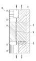
- FIG. 1 is a schematic structural explanatory view schematically showing the main part of the structure of an accumulation type MOSFET according to a preferred embodiment of the present invention.
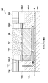
- FIG. 2 is a schematic explanatory diagram for explaining a current path near the threshold voltage (during switching).
- FIG. 3 is a schematic explanatory diagram for explaining a current path in an ON state (operation state).
- FIG. 1 is a schematic structural explanatory view schematically showing the main part of the structure of one Accumulation type MOSFET according to a preferred embodiment of the present invention.
- An A-type MOSFET 100 shown in FIG. 1 includes an n ⁇ silicon (Si) semiconductor region (hereinafter simply referred to as “n ⁇ ”) in which a channel region is formed on a BOX (Buried oxide) layer 101 made of SiO 2 (silicon oxide) or the like. 102 ”, two n + silicon (Si) semiconductor regions for forming ohmic contacts (hereinafter also simply referred to as“ n + region ”) 103-1, 103-2, It has.
- the BOX layer 101 is provided by a normal semiconductor manufacturing technique using a silicon (Si) semiconductor substrate.
- a typical example is an SOI (Silicon on Insulator) substrate prepared by a bonding method.
- Two Si semiconductor substrates having a SiO 2 layer having a predetermined thickness formed by oxidizing the surface in advance on the surface are prepared and bonded together with the SiO 2 layers on the surface inside. Thereafter, the surface of the Si semiconductor region of one Si semiconductor substrate is polished by CMP or the like to form a Si semiconductor region layer having a predetermined thickness.
- the source electrode 104 passes through the silicide region 106-1, and in the n + region (drain region) 103-2, the drain electrode 105 passes through the silicide region 106-2. Are electrically connected to each other.
- a gate electrode 108 is provided on the n ⁇ region 102 with a gate insulating layer 107 interposed therebetween.
- the gate insulating layer 107 and the gate electrode 108 are electrically insulated from the source electrode 104, the drain electrode 105, and the silicide regions 106-1 and 106-2 by the insulating regions 109-1 and 109-2.
- the silicide region 106-1 is formed so that an ohmic contact is formed in “source electrode 104 / silicide region 106-1 / n + region 103-1 / n ⁇ region 102”, and the silicide region 106-2 is In “drain electrode 105 / silicide region 106-2 / n + region 103-2 / n ⁇ region 102”, each is provided according to desired conditions so that an ohmic contact is formed.
- n + regions 103-1 and 103-2 are provided between the source electrode 104 and the n ⁇ region 102 and between the drain electrode 105 and the n ⁇ region 102 by providing the silicide regions 106-1 and 106-2. If a good ohmic contact is formed, it is not always necessary.
- a structural feature of the A-type MOSFET 100 shown in FIG. 1 is that a p + buried region 110 is provided in the n ⁇ region 102 in contact with the n + region 103-1. Further, the p + buried region 110 is opposed to the insulating region 109-1 with a part of the n ⁇ region 102 interposed therebetween.
- the source electrode 104 and the drain electrode 105 are metals normally used in the semiconductor field, such as tungsten (W), aluminum (Al), copper (Cu), nickel (Ni), etc., and polysilicon (poly-Si). ) Etc.
- an appropriate constituent material is selected so that an electrical contact between the n + region 103 and the source electrode 104 and the drain electrode 105 becomes an ohmic contact.
- the silicide region 106 has a thickness sufficient to form a silicide region 106 having a predetermined thickness, and a metal layer that may also be a part of the source or drain electrode on the n + region provided on the BOX layer 101.
- This is a diffusion region formed by thermal diffusion of silicon (Si) in the n + region and metal of the metal layer (hereinafter also referred to as “M”) by performing a heat treatment after the sputtering method.
- a low work function metal such as holmium (Ho), erbium (Er), samarium (Sm), yttrium (Yb), or the like is preferably used for the metal layer. In particular, holmium (Ho) and erbium (Er) are desirable.
- the silicide region 106-1 and the silicide region 106-2 may be the same or different as long as appropriate ohmic contacts can be formed.
- the gate insulating layer 107 interposed between the n ⁇ region 102 and the gate electrode 108 is formed of a dense and electrically insulating material such as silicon oxide, silicon nitride, or silicon oxynitride.
- the gate electrode 108 is usually composed of polysilicon (poly-Si), but in addition, a refractory metal such as tungsten (W) and tantalum (Ta), a metal such as titanium (Ti) and aluminum (Al), and the like. It can also be comprised with the compound.
- the A-type MOSFET shown in FIG. 1 is produced by ordinary semiconductor technology.
- the illustrated MOSFET 100 is formed on a BOX layer 101 having a thickness of about 50 nm, for example, on the surface of a support substrate (not shown) formed using a p-type silicon substrate.
- An n ⁇ semiconductor region 102 is formed on the BOX layer 101, and a channel region is formed therein.
- the n ⁇ semiconductor region 102 has a film thickness of 50 nm, for example.
- n + region 103-1 On both sides of the n ⁇ type semiconductor region 102, a source region (n + region 103-1) / drain region (contained by an n + semiconductor having the same conductivity type as that of the channel region and having an impurity atom concentration higher than that of the channel region) n + region 103-2).
- n ⁇ semiconductor region 102 On the n ⁇ semiconductor region 102, for example, a gate insulating layer 107 made of an oxide film having an electrical equivalent film thickness (EOT) of 7.5 nm is provided, and on the gate insulating layer 107, p A gate electrode 108 made of + polysilicon is provided.
- the illustrated n-channel transistor has a gate length and a gate width of, for example, 0.6 ⁇ m and 20.0 ⁇ m, respectively.
- the average impurity atom concentration of the n ⁇ semiconductor region 102 is, for example, about 2 ⁇ 10 17 cm ⁇ 3
- the average impurity atom concentration of the n + regions 103-1 and 103-2 is, for example, It is about 2 ⁇ 10 20 cm ⁇ 3 .
- the source region 103-1, the drain region 103-2, and the silicide regions 106-1 and 106-2 are a low work function metal layer on the n + region, an antioxidant metal layer serving as a source electrode and a drain electrode (in the present invention). Is typically employed in order to cause a silicidation reaction between the n + region and the low work function metal layer by performing a heat treatment in a stacked state of tungsten (W). It is formed.
- the material of the low work function metal layer is smaller than the value obtained by adding 0.3 eV to the absolute value of the energy at the bottom of the conduction band of n + silicon constituting the source region 106-1 and the drain region 106-2. It is desirable to select from a metal material having a work function. As such a metal material, holmium (Ho) or erbium (Er) is particularly preferable.
- a sputtering method is desirable as a method for forming the metal layer in order to suppress the contamination of impurities as much as possible.
- holmium (Ho) is deposited to a thickness of 10 nm by sputtering in an Ar atmosphere.
- the atmosphere of sputtering may be Xe, and erbium (Er) may be used instead of holmium (Ho) as previously performed.
- holmium (Ho) or erbium (Er) is desirable as the material exceeding 700 ° C., but other rare earth metals such as samarium (Sm) and ytterbium (Yb) can also be used.
- the low work function metal layer has an absolute value higher than the value obtained by adding 0.3 eV to the absolute value of the energy at the bottom of the conduction band of silicon. It may be formed of a metal material having a small work function.
- the contact resistance with the n ⁇ semiconductor region 102 is suppressed to 1 ⁇ 10 ⁇ 9 ⁇ cm 2 or less, and the series resistance with the source region 103-1 and the drain region 103-2 as n + regions is reduced. Even when combined, the series resistance of the transistor can be 1.0 ⁇ m.
- a part of the low work function metal layer is formed on the surface of the n + region that forms the source region 103-1 and the drain region 103-2 in the metal forming apparatus.
- the low work function metal layer After the low work function metal layer is formed, it is transported in an inert gas atmosphere such as nitrogen or argon under reduced pressure so as not to be exposed to the atmosphere, and is carried into the formation chamber of the antioxidation metal layer. 1.
- An antioxidant metal layer is formed on the entire exposed surface of the n + region for forming the drain region 103-2. The formation of the antioxidant metal layer in this case is performed, for example, by using tungsten (W) and sputtering tungsten (W) by 300 nm in an argon (Ar) atmosphere in the sputtering chamber.
- the low work function metal layer and the antioxidant metal layer are heat-treated (annealed) at, for example, 600 ° C. to form a silicide layer region such as holmium (Ho) silicide as described above.
- the annealing is preferably performed, for example, in an Ar or N 2 atmosphere at 300 to 700 ° C. for 2 to 60 minutes. More preferably, in the case of holmium (Ho) and erbium (Er), it is desirable to anneal at 600 ° C. for about 10 minutes.
- the thickness of the antioxidant metal layer thicker than the thickness of the low work function metal layer, the surface roughness of the silicide layer can be reduced and the destruction of the pn junction can be prevented.
- holmium (Ho) or erbium (Er) constituting the low work function metal layer is oxidized during annealing, and a high-quality silicide thin film of a metal having a desired low work function is formed.
- the W layer is provided, the oxidation of holmium (Ho) or erbium (Er) is suppressed, and the silicide thin film to be formed does not have any defect or does not substantially occur. It is possible to form a high-quality silicide thin film of a metal having As a result, a high-quality silicide thin film with a low work function is formed.
- the thickness of the anti-oxidation metal layer is low so that the constituent metal of the low work function metal layer does not hinder the formation of flatness at the interface between the silicide region and the n + silicon layer region formed by migration during annealing. It is appropriately selected depending on the thickness of the work function metal layer.
- the thickness of the W layer is preferably 100 nm or more, and the effect obtained in that case is remarkable.
- the thickness (t) (distance (L)) is preferably set to about the thickness of the storage layer formed under the gate insulating layer 107, more preferably about several to 10 nm. It is desirable to do.
- the thickness is too small, the electrons will not be emitted by thermionic emission from the n + region 103-1) or the silicide region (106-1) when turned on, and the ON current will be reduced. When it becomes thicker than about 10 nm, the so-called tunnel effect is not expected.
- the present invention is applied to an A-type n-channel MOSFET has been described above, but the present invention can be applied to an A-type p-channel MOSFET as well.
- the example of the Si semiconductor is used as the semiconductor.
- other semiconductors such as Ge, SiGe, SiC, and the like can be used.
- Step 1 n - well (3e17 cm ⁇ 3 ) is formed on the SOI substrate
- Step 2 Separation: Etching of silicon part other than the active region (plasma etching using (Ar / HBr) gas)
- Step 3 Gate oxidation (1.5 nm, 400 ° C., radical oxidation).
- a high-k film may be formed.
- “Process 4” Poly-Si deposition (150 nm thickness, 530 ° C., SiH 4 )
- “Process 5” Boron ion (B + ) implantation (5e15 cm ⁇ 2 , 10 keV)
- “Step 6” Gate Poly-Si etching (Ar / HBr)
- Step 7 BF 2 injection (1E15cm -2 (tilt7 °))
- Step 8 Side wall formation: Si 3 N 4 (SiH 4 , N 2 , H 2 plasma CVD) + Dry etching (C 5 F 8 )
- Step 11 patterning + W wet etching (alkali etching) + Er wet etch etch
- FIGS. 2 is a schematic explanatory diagram for explaining a current path in the vicinity of a threshold voltage (during switching)
- FIG. 3 is a schematic explanatory diagram for explaining a current path in an ON state (operation state).
- the numbers common to those in FIG. 1 are the same as those shown in FIG.
- the potential of the gate electrode 108 changes as the electric charge is accumulated in the gate electrode 108, and eventually reaches the power supply voltage.
- this process until the potential of the gate electrode 108 reaches the power supply voltage may be referred to as a transition process.
- the current path at the applied voltage (power supply voltage) (“ON voltage” or “operating voltage”) to be turned on (operating state) is indicated by an arrow in FIG.
- a current (accumulation region current) based on the charges accumulated in the accumulation region starts to flow.
- the bulk current flowing from the transition process continues to flow even when the gate voltage becomes the power supply voltage.
- the current tunnels through the p + buried region through the path “n + region 103-1 ⁇ p + buried region 110 ⁇ n ⁇ region 102”.
- carriers are injected from the n + region 103-1 into the n ⁇ region 102 to form a so-called tunnel current, so that there is no limit of 60 mV / dec at room temperature, and the potential barrier formed in the p + buried region 11 the by appropriately controlled by the width of the p + buried region 11, can be changed from the OFF state to the oN state in the following slope 60 mV / dec.
- MOSFET 101 MOSFET 101 ... BOX layer 102 ... n - region 103 ... n + region 104 ... source electrode 105 ... drain electrode 106 ... silicide region 107 ... insulating layer 108 ... gate electrode 109 ... Insulating region 110 ... p + buried region
Landscapes
- Thin Film Transistor (AREA)
- Electrodes Of Semiconductors (AREA)
Abstract
Description
しかし、非特許文献1、2に記載のA型MOSFETでは、熱電子放出によるキャリア移動であるためS値(ドレイン電流を一桁上げるためのゲート電圧)が60mV/dec以上(室温)である。
「工程2」:分離:活性領域以外のシリコン部分をエッチング((Ar/HBr)ガスを用いたプラズマエッチング)
「工程3」:ゲート酸化(1.5nm、400℃、ラジカル酸化)。High-k膜の成膜でも良い。
「工程4」:Poly-Siデポジッション(150nm厚、530℃、SiH4)
「工程5」:ボロンイオン(B+)注入(5e15cm-2、10keV)
「工程6」:ゲートPoly-Siエッチング(Ar/HBr)
「工程7」:BF2注入(1E15cm-2(tilt7°))
「工程8」:サイドウォール形成:Si3N4(SiH4、N2、H2プラズマCVD)+Dryエッチング
(C5F8)
「工程9」:As注入(3e15cm-2、25KeV(tilt0°))
「工程10」:Erスパッタ成膜(W/Er=100/5nm)+アニール500℃、2min
「工程11」:パターニング+Wウェットエッチング(アルカリエッチング)+Erウェットエッチング(室温H2SO4+H2O2)
「工程12」:活性化アニール、N2、1000℃、5sec
「工程13」:再酸化(ラジカル酸化7nm)
「工程14」:CVD-SiO2、300nm
「工程15」:コンタクトホール形成、ドライエッチング(C5F8)
「工程16」:Al成膜 500nm
「工程17」:Alエッチング
101・・・BOX層
102・・・n-領域
103・・・n+領域
104・・・ソース電極
105・・・ドレイン電極
106・・・シリサイド領域
107・・・絶縁層
108・・・ゲート電極
109・・・絶縁領域
110・・・p+埋め込み領域
Claims (4)
- トンネル電子放出部と熱電子放出部とをソース領域部に設けたことを特徴とするAccumulation型MOSFET。
- 前記トンネル電子放出部と前記熱電子放出部とで2層構造を構成している請求項1に記載のAccumulation型MOSFET。
- トンネル電子放出部と熱電子放出部とをソース領域部に設けたAccumulation型MOSFETを、OFF状態からON状態への遷移時にはトンネル電流によって駆動し、ON状態では熱電子電流によって駆動することを特徴とするAccumulation型MOSFETの駆動方法。
- OFF状態からON状態に遷移するときのドレイン電流を一桁上昇させるために必要なゲート電圧が少なくとも室温で60mVより小さくなる領域が存在することを特徴とする請求項3に記載のMOSFETの駆動方法。
Priority Applications (5)
| Application Number | Priority Date | Filing Date | Title |
|---|---|---|---|
| PCT/JP2012/006858 WO2014064737A1 (ja) | 2012-10-25 | 2012-10-25 | Accumulation型MOSFET |
| JP2013557318A JP5704586B2 (ja) | 2012-10-25 | 2012-10-25 | Accumulation型MOSFET |
| KR1020157007616A KR101529023B1 (ko) | 2012-10-25 | 2012-10-25 | Accumulation형 MOSFET |
| TW102137499A TWI503986B (zh) | 2012-10-25 | 2013-10-17 | Polarization of gold and oxygen halide effect transistor |
| US14/636,817 US9299844B2 (en) | 2012-10-25 | 2015-03-03 | Accumulation-mode MOSFET and driving method thereof |
Applications Claiming Priority (1)
| Application Number | Priority Date | Filing Date | Title |
|---|---|---|---|
| PCT/JP2012/006858 WO2014064737A1 (ja) | 2012-10-25 | 2012-10-25 | Accumulation型MOSFET |
Related Child Applications (1)
| Application Number | Title | Priority Date | Filing Date |
|---|---|---|---|
| US14/636,817 Continuation US9299844B2 (en) | 2012-10-25 | 2015-03-03 | Accumulation-mode MOSFET and driving method thereof |
Publications (1)
| Publication Number | Publication Date |
|---|---|
| WO2014064737A1 true WO2014064737A1 (ja) | 2014-05-01 |
Family
ID=50544141
Family Applications (1)
| Application Number | Title | Priority Date | Filing Date |
|---|---|---|---|
| PCT/JP2012/006858 Ceased WO2014064737A1 (ja) | 2012-10-25 | 2012-10-25 | Accumulation型MOSFET |
Country Status (5)
| Country | Link |
|---|---|
| US (1) | US9299844B2 (ja) |
| JP (1) | JP5704586B2 (ja) |
| KR (1) | KR101529023B1 (ja) |
| TW (1) | TWI503986B (ja) |
| WO (1) | WO2014064737A1 (ja) |
Cited By (4)
| Publication number | Priority date | Publication date | Assignee | Title |
|---|---|---|---|---|
| US20160020305A1 (en) * | 2014-07-21 | 2016-01-21 | Samsung Electronics Co., Ltd. | Thermionically-overdriven tunnel fets and methods of fabricating the same |
| US9484423B2 (en) | 2013-11-01 | 2016-11-01 | Samsung Electronics Co., Ltd. | Crystalline multiple-nanosheet III-V channel FETs |
| JP2017028006A (ja) * | 2015-07-17 | 2017-02-02 | 国立大学法人東北大学 | 電界効果トランジスタおよびその駆動方法 |
| US9570609B2 (en) | 2013-11-01 | 2017-02-14 | Samsung Electronics Co., Ltd. | Crystalline multiple-nanosheet strained channel FETs and methods of fabricating the same |
Families Citing this family (1)
| Publication number | Priority date | Publication date | Assignee | Title |
|---|---|---|---|---|
| US10134863B2 (en) | 2015-06-15 | 2018-11-20 | Taiwan Semiconductor Manufacturing Company, Ltd. | Vertical semiconductor device structure and method of forming |
Citations (5)
| Publication number | Priority date | Publication date | Assignee | Title |
|---|---|---|---|---|
| JPH0491480A (ja) * | 1990-08-03 | 1992-03-24 | Hitachi Ltd | 半導体装置 |
| WO2005083796A1 (ja) * | 2004-02-27 | 2005-09-09 | Rohm Co., Ltd. | 半導体装置およびその製造方法 |
| WO2008007749A1 (en) * | 2006-07-13 | 2008-01-17 | National University Corporation Tohoku University | Transistor and semiconductor device |
| WO2010050405A1 (ja) * | 2008-10-30 | 2010-05-06 | 国立大学法人東北大学 | コンタクト形成方法、半導体装置の製造方法、および半導体装置 |
| JP2011181617A (ja) * | 2010-02-26 | 2011-09-15 | Toshiba Corp | 半導体装置及びその製造方法 |
Family Cites Families (7)
| Publication number | Priority date | Publication date | Assignee | Title |
|---|---|---|---|---|
| US5581100A (en) * | 1994-08-30 | 1996-12-03 | International Rectifier Corporation | Trench depletion MOSFET |
| US5844273A (en) * | 1994-12-09 | 1998-12-01 | Fuji Electric Co. | Vertical semiconductor device and method of manufacturing the same |
| US5920088A (en) * | 1995-06-16 | 1999-07-06 | Interuniversitair Micro-Electronica Centrum (Imec Vzw) | Vertical MISFET devices |
| US6191447B1 (en) * | 1999-05-28 | 2001-02-20 | Micro-Ohm Corporation | Power semiconductor devices that utilize tapered trench-based insulating regions to improve electric field profiles in highly doped drift region mesas and methods of forming same |
| US7638841B2 (en) * | 2003-05-20 | 2009-12-29 | Fairchild Semiconductor Corporation | Power semiconductor devices and methods of manufacture |
| US8878292B2 (en) * | 2008-03-02 | 2014-11-04 | Alpha And Omega Semiconductor Incorporated | Self-aligned slotted accumulation-mode field effect transistor (AccuFET) structure and method |
| JP2009302510A (ja) * | 2008-03-03 | 2009-12-24 | Fuji Electric Device Technology Co Ltd | トレンチゲート型半導体装置およびその製造方法 |
-
2012
- 2012-10-25 JP JP2013557318A patent/JP5704586B2/ja active Active
- 2012-10-25 KR KR1020157007616A patent/KR101529023B1/ko active Active
- 2012-10-25 WO PCT/JP2012/006858 patent/WO2014064737A1/ja not_active Ceased
-
2013
- 2013-10-17 TW TW102137499A patent/TWI503986B/zh active
-
2015
- 2015-03-03 US US14/636,817 patent/US9299844B2/en active Active
Patent Citations (5)
| Publication number | Priority date | Publication date | Assignee | Title |
|---|---|---|---|---|
| JPH0491480A (ja) * | 1990-08-03 | 1992-03-24 | Hitachi Ltd | 半導体装置 |
| WO2005083796A1 (ja) * | 2004-02-27 | 2005-09-09 | Rohm Co., Ltd. | 半導体装置およびその製造方法 |
| WO2008007749A1 (en) * | 2006-07-13 | 2008-01-17 | National University Corporation Tohoku University | Transistor and semiconductor device |
| WO2010050405A1 (ja) * | 2008-10-30 | 2010-05-06 | 国立大学法人東北大学 | コンタクト形成方法、半導体装置の製造方法、および半導体装置 |
| JP2011181617A (ja) * | 2010-02-26 | 2011-09-15 | Toshiba Corp | 半導体装置及びその製造方法 |
Cited By (4)
| Publication number | Priority date | Publication date | Assignee | Title |
|---|---|---|---|---|
| US9484423B2 (en) | 2013-11-01 | 2016-11-01 | Samsung Electronics Co., Ltd. | Crystalline multiple-nanosheet III-V channel FETs |
| US9570609B2 (en) | 2013-11-01 | 2017-02-14 | Samsung Electronics Co., Ltd. | Crystalline multiple-nanosheet strained channel FETs and methods of fabricating the same |
| US20160020305A1 (en) * | 2014-07-21 | 2016-01-21 | Samsung Electronics Co., Ltd. | Thermionically-overdriven tunnel fets and methods of fabricating the same |
| JP2017028006A (ja) * | 2015-07-17 | 2017-02-02 | 国立大学法人東北大学 | 電界効果トランジスタおよびその駆動方法 |
Also Published As
| Publication number | Publication date |
|---|---|
| TW201436219A (zh) | 2014-09-16 |
| US20150179788A1 (en) | 2015-06-25 |
| US9299844B2 (en) | 2016-03-29 |
| JP5704586B2 (ja) | 2015-04-22 |
| TWI503986B (zh) | 2015-10-11 |
| KR101529023B1 (ko) | 2015-06-15 |
| JPWO2014064737A1 (ja) | 2016-09-05 |
| KR20150039876A (ko) | 2015-04-13 |
Similar Documents
| Publication | Publication Date | Title |
|---|---|---|
| TWI390630B (zh) | 半導體元件的製造方法 | |
| JP5042943B2 (ja) | デュアルゲートを有するcmos型半導体装置形成方法 | |
| CN103681276B (zh) | 金属栅极、mos晶体管及cmos结构分别的形成方法 | |
| CN101840862B (zh) | 高性能半导体器件的形成方法 | |
| JP5704586B2 (ja) | Accumulation型MOSFET | |
| US20250006499A1 (en) | Integrated dipole region for transistor | |
| US9911821B2 (en) | Semiconductor device structure and method for forming the same | |
| JP5126930B2 (ja) | 半導体装置の製造方法 | |
| JP2004247341A (ja) | 半導体装置 | |
| JP2008053283A (ja) | 半導体装置の製造方法 | |
| JP5252627B2 (ja) | 半導体装置の製造方法および半導体装置 | |
| JP5437592B2 (ja) | 半導体装置およびその製造方法 | |
| JP2015084436A (ja) | Accumulation型MOSFET | |
| JP6487288B2 (ja) | 電界効果トランジスタおよびその駆動方法 | |
| US7456115B2 (en) | Method for forming semiconductor devices having reduced gate edge leakage current | |
| JP2007281318A (ja) | 半導体装置の製造方法 | |
| TWI922708B (zh) | 用於可靠低接觸電阻之導電氧矽化物 | |
| US20250048683A1 (en) | Methods of forming electronic devices having a strained transistor channel | |
| US20260101550A1 (en) | Semiconductor devices with mixed channel | |
| US20240222195A1 (en) | Dipole formation processes | |
| JP2008072001A (ja) | 半導体装置及びその製造方法 | |
| JPH05109652A (ja) | 半導体装置の製造方法 | |
| TW202429549A (zh) | 金屬閘極堆疊的自由基處理 |
Legal Events
| Date | Code | Title | Description |
|---|---|---|---|
| ENP | Entry into the national phase |
Ref document number: 2013557318 Country of ref document: JP Kind code of ref document: A |
|
| 121 | Ep: the epo has been informed by wipo that ep was designated in this application |
Ref document number: 12886995 Country of ref document: EP Kind code of ref document: A1 |
|
| ENP | Entry into the national phase |
Ref document number: 20157007616 Country of ref document: KR Kind code of ref document: A |
|
| NENP | Non-entry into the national phase |
Ref country code: DE |
|
| 122 | Ep: pct application non-entry in european phase |
Ref document number: 12886995 Country of ref document: EP Kind code of ref document: A1 |