WO2014050276A1 - 電力変換装置 - Google Patents
電力変換装置 Download PDFInfo
- Publication number
- WO2014050276A1 WO2014050276A1 PCT/JP2013/069971 JP2013069971W WO2014050276A1 WO 2014050276 A1 WO2014050276 A1 WO 2014050276A1 JP 2013069971 W JP2013069971 W JP 2013069971W WO 2014050276 A1 WO2014050276 A1 WO 2014050276A1
- Authority
- WO
- WIPO (PCT)
- Prior art keywords
- flow path
- forming body
- power semiconductor
- path forming
- base plate
- Prior art date
- Legal status (The legal status is an assumption and is not a legal conclusion. Google has not performed a legal analysis and makes no representation as to the accuracy of the status listed.)
- Ceased
Links
Images



Classifications
-
- H—ELECTRICITY
- H02—GENERATION; CONVERSION OR DISTRIBUTION OF ELECTRIC POWER
- H02M—APPARATUS FOR CONVERSION BETWEEN AC AND AC, BETWEEN AC AND DC, OR BETWEEN DC AND DC, AND FOR USE WITH MAINS OR SIMILAR POWER SUPPLY SYSTEMS; CONVERSION OF DC OR AC INPUT POWER INTO SURGE OUTPUT POWER; CONTROL OR REGULATION THEREOF
- H02M7/00—Conversion of AC power input into DC power output; Conversion of DC power input into AC power output
- H02M7/003—Constructional details, e.g. physical layout, assembly, wiring or busbar connections
-
- H—ELECTRICITY
- H05—ELECTRIC TECHNIQUES NOT OTHERWISE PROVIDED FOR
- H05K—PRINTED CIRCUITS; CASINGS OR CONSTRUCTIONAL DETAILS OF ELECTRIC APPARATUS; MANUFACTURE OF ASSEMBLAGES OF ELECTRICAL COMPONENTS
- H05K7/00—Constructional details common to different types of electric apparatus
- H05K7/14—Mounting supporting structure in casing or on frame or rack
- H05K7/1422—Printed circuit boards receptacles, e.g. stacked structures, electronic circuit modules or box like frames
- H05K7/1427—Housings
- H05K7/1432—Housings specially adapted for power drive units or power converters
- H05K7/14322—Housings specially adapted for power drive units or power converters wherein the control and power circuits of a power converter are arranged within the same casing
-
- H—ELECTRICITY
- H05—ELECTRIC TECHNIQUES NOT OTHERWISE PROVIDED FOR
- H05K—PRINTED CIRCUITS; CASINGS OR CONSTRUCTIONAL DETAILS OF ELECTRIC APPARATUS; MANUFACTURE OF ASSEMBLAGES OF ELECTRICAL COMPONENTS
- H05K7/00—Constructional details common to different types of electric apparatus
- H05K7/20—Modifications to facilitate cooling, ventilating, or heating
- H05K7/20218—Modifications to facilitate cooling, ventilating, or heating using a liquid coolant without phase change in electronic enclosures
-
- H—ELECTRICITY
- H05—ELECTRIC TECHNIQUES NOT OTHERWISE PROVIDED FOR
- H05K—PRINTED CIRCUITS; CASINGS OR CONSTRUCTIONAL DETAILS OF ELECTRIC APPARATUS; MANUFACTURE OF ASSEMBLAGES OF ELECTRICAL COMPONENTS
- H05K7/00—Constructional details common to different types of electric apparatus
- H05K7/20—Modifications to facilitate cooling, ventilating, or heating
- H05K7/2089—Modifications to facilitate cooling, ventilating, or heating for power electronics, e.g. for inverters for controlling motor
- H05K7/20927—Liquid coolant without phase change
Definitions
- the present invention relates to a power conversion device that converts DC power into AC power or converts AC power into DC power, and more particularly to a power conversion device used in a hybrid vehicle or an electric vehicle.
- an object of the present invention is to further improve the assemblability of the power conversion device.
- a power conversion device includes a power semiconductor module having a power semiconductor element that converts a direct current into an alternating current, a first flow path forming body that forms a first flow path through which a cooling refrigerant flows, and a cooling refrigerant.
- a drive circuit including a second flow path forming body that forms the second flow path, a first base plate on which the second flow path forming body is mounted, and a drive circuit that outputs a drive signal for driving the power semiconductor element A board, a case for housing the power semiconductor module, the first flow path forming body, the second flow path forming body, the first base plate, and the drive circuit board, and the drive circuit board includes:
- the mounting surface of the drive circuit is disposed so as to face the side wall of the second flow path forming body, the second flow path forming body forms a storage space for storing the power semiconductor module, and further, the second flow The path forming body is stored in the storage
- An insertion port connected to the drive circuit is formed in the side wall facing the mounting surface of the drive circuit, and the power semiconductor module has a control terminal connected to the drive circuit board through the insertion port, the first
- the flow path forming body is fixed to the case, and further, the first flow path forming body forms an opening connected to the first flow path, and the first base plate
- the assemblability of the power conversion device can be improved.
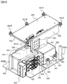
- FIG. 3 is an enlarged perspective view of an electrical component disposed between a first flow path forming body 110 and a cover 107 shown in FIG. 2.
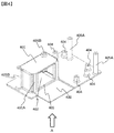
- FIG. 4 is an enlarged perspective view of a first base plate 400 and a second flow path forming body 401 shown in FIG. 2.
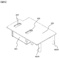
- FIG. 5 is an external perspective view of a first base plate 400 viewed from the direction of arrow A in FIG. 4.
- 2 is an external perspective view of a case 101 and a first flow path forming body 110.
- FIG. FIG. 6 is an external perspective view showing a process of housing the first base plate 400 and the like in the case 101.
- FIG. 1 is an external perspective view of a power conversion apparatus 100 according to the present embodiment.
- Case 101 houses a power semiconductor module 300U and the like which will be described later.
- the outlet pipe 103 discharges the cooling refrigerant to the outside of the power conversion apparatus 100.
- the outlet pipe 103 is disposed around the center of the case side surface 101A in the height direction.
- the inlet pipe 102 (see FIG. 2) is arranged around the center in the height direction of the case side surface 101B formed on the side opposite to the case side surface 101A.
- the inlet pipe 102 introduces the cooling refrigerant into the power conversion apparatus 100.
- the case 101 has an opening 105 formed on the case side surface 101C.
- the AC bus bar 104U, the AC bus bar 104V, and the AC bus bar 104W protrude from the inside of the case 101 to the outside of the case 101 through the opening 105.
- the AC bus bar 104U is a conductor member that transmits a U-phase AC current
- the AC bus bar 104V is a conductor member that transmits a V-phase AC current
- the AC bus bar 104W is a conductor member that transmits a W-phase AC current. .
- the case 101 forms an opening 106 on the case side surface 101A.
- the opening 106 is formed at a position facing a connection portion between the AC bus bar 104U and another conductor, a connection portion between the AC bus bar 104V and another conductor, and a connection portion between the AC bus bar 104W and another conductor.
- a worker or a work robot can perform a connection work between the AC bus bar and another conductor through the opening 106.
- the cover 107 closes the first insertion port 109 (see FIG. 2) formed in the upper part of the case 101.
- the first insertion port 109 is formed to accommodate a power semiconductor module 300U and the like which will be described later.
- the cover 108 closes a second insertion port (not shown) formed in the lower part of the case 101.
- the second insertion opening is formed to accommodate a DCDC converter 900 described later.
- the power conversion device 100 according to the present embodiment is mainly used for a hybrid vehicle and an electric vehicle.
- An example of the vehicle system is described in Japanese Patent Application Laid-Open No. 2011-217550.
- the power converter device 100 which concerns on this embodiment may be used for another use in order to achieve the effect.
- it may be used for a home appliance inverter of a refrigerator or an air conditioner for the purpose of improving productivity and cooling performance.
- the inverter may be used for an inverter for industrial equipment whose use environment is similar to that for a vehicle inverter.
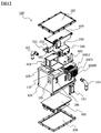
- FIG. 2 is an exploded perspective view of the power conversion apparatus 100 according to the present embodiment.
- the first flow path forming body 110 is disposed around the middle in the height direction of the case 101.
- the first flow path forming body 110 is connected to the inlet pipe 102 and the outlet pipe 103. Between the first flow path forming body 110 and the cover 107, the first base plate 400, the second flow path forming body 401, the power semiconductor modules 300U to 300W, the capacitor module 500, the drive circuit board 200, and the control circuit board 600 are provided. Etc. are arranged.
- the power semiconductor modules 300U to 300W described later convert a direct current into an alternating current.
- the capacitor module 500 described later smoothes the DC voltage.
- the drive circuit board 200 is mounted with a drive circuit that outputs a drive signal for driving the power semiconductor modules 300U to 300W.
- the control circuit board 600 includes a control circuit that outputs a control signal for controlling the power semiconductor modules 300U to 300W on the drive circuit board 200. An example of these circuit systems is described in JP 2011-217550 A.
- a DCDC converter 900 is disposed between the first flow path forming body 110 and the cover 108.
- the DCDC converter 900 converts a direct current voltage.
- An example of a circuit system of the DCDC converter 900 is described in Japanese Patent Publication No. 4463695.
- the opening 106 illustrated in FIG. 1 is closed by the cover 111.
- FIG. 3 is an enlarged perspective view of an electrical component disposed between the first flow path forming body 110 and the cover 107 shown in FIG.
- FIG. 4 is an enlarged perspective view of the first base plate 400 and the second flow path forming body 401 shown in FIG.
- the second flow path forming body 401 is mounted on the first base plate 400.
- the second flow path forming body 401 and the first base plate 400 may be integrally formed in order to improve productivity and thermal conductivity.
- the second flow path forming body 401 forms a storage space 402 for storing the power semiconductor modules 300U to 300W.
- the second flow path forming body 401 forms an insertion port 403 connected to the storage space 402 on the side wall 401A.
- the storage space 402 functions as a flow path for flowing the cooling refrigerant.
- the insertion port 403 is one insertion port for inserting three power semiconductor modules 300U to 300W, but may be provided for each of a plurality of power semiconductor modules.
- the first base plate 400 has a plurality of support members 404 for fixing the capacitor module 500.
- the capacitor module 500 is fixed in a state where it is thermally connected to the first base plate 400 by a plurality of support members 404. Thereby, the heat generated in the capacitor module 500 is transmitted to the first base plate 400, and the capacitor module 500 can be cooled.
- the second base plate 601 mounts the control circuit board 600.
- the second base plate 601 includes a fixing portion 601A connected to a support member 405A extending from the first base plate 400.
- the control circuit board 600 and the like are cooled by the first base plate 400 via the fixed portion 601A and the support member 405A.
- the second base plate 601 supports the third base plate 602.
- the third base plate 602 projects in the direction perpendicular to the mounting surface of the control circuit board 600 on the second base plate 601 and in the arrangement direction of the first base plate 400.
- the drive circuit board 200 is mounted on the surface of the third base plate 602 on the side where the power semiconductor modules 300U to 300W are disposed. As a result, the drive circuit board 200 is cooled by the third base plate 602 and the second base plate 601.
- the second base plate 601 has a fixing portion 601B connected to a support member 405B extending from the second flow path forming body 401. As a result, the second base plate 601 is thermally connected to the second flow path forming body 401 via the fixing portion 601B, so that the cooling performance of the control circuit board 600 or the drive circuit board 200 can be improved. .
- the second base plate 601 and the third base plate 602 are made of a material having high electrical conductivity such as aluminum.
- the case 101 illustrated in FIG. 1 is made of a material having high electrical conductivity such as aluminum.
- the second base plate 601 has a fixing portion 601 ⁇ / b> C that is directly connected to the case 101.
- the control circuit board 600 is disposed on the opposite side of the power semiconductor modules 300U to 300W with the second base plate 601 interposed therebetween. As a result, electromagnetic noise radiated from the power semiconductor modules 300U to 300W and the drive circuit board 200 can be caused to flow to the ground via the fixed portion 601C and the like, so that the control circuit board 600 can be protected from the electromagnetic noise.
- the drive circuit board 200 is disposed such that the mounting surface of the drive circuit faces the side wall 401A of the second flow path forming body 401.
- the power semiconductor modules 300U to 300W have a control terminal 325 connected to the drive circuit board 200 through the insertion port 403.
- the connection work between the control terminal 325 and the drive circuit board 200 is performed before the power semiconductor modules 300U to 300W and the drive circuit board 200 are mounted on the case 101.
- the third base plate 602 forms an opening 603 formed at a position facing the connection portion 201 between the control terminal 325 and the drive circuit board 200.
- the current sensor 202 is arranged so that a through hole formed in the current sensor 202 is penetrated by the AC bus bars 104U to 104W.
- the capacitor module 500 includes a resin sealing body 503 that seals a part of the DC positive terminal 501 and a part of the DC negative terminal 502.
- the resin sealing body 503 in the resin sealing body 503, one surface of the resin sealing body 503 is in contact with one surface of the second flow path forming body 401. As a result, the resin sealing body 503 is cooled, and the DC positive terminal 501 and the DC negative terminal 502 are also cooled.
- FIG. 5 is an external perspective view of the first base plate 400 viewed from the direction of arrow A in FIG.
- the first base plate 400 forms a first through hole 406 that is connected to the storage space 402.
- the first base plate 400 forms a second through hole 407 that is connected to the storage space 402.
- FIG. 6 is an external perspective view of the case 101 and the first flow path forming body 110.
- the first flow path forming body 110 is formed integrally with the case 101.
- the case 101 and the first flow path forming body 110 are manufactured by casting. This eliminates the fastening material (bolts and the like), thereby reducing the weight. Moreover, the heat conduction between the case 101 and the first flow path forming body 110 becomes good, and the cooling performance of the entire power conversion device 100 is improved.
- the first flow path forming body 110 forms a flow path 112a connected to the inlet pipe 102.
- the flow path 112a is formed so as to be connected to the first through hole 406 shown in FIG.
- the first flow path forming body 110 forms a flow path 112b on the side of the flow path 112a with the partition wall 113 interposed therebetween.
- the flow path 112b is formed so as to be connected to the second through hole 407 shown in FIG.
- the first flow path forming body 110 forms a flow path 112 c that is connected to the flow path 112 b and is connected to the outlet pipe 103.
- the flow path 112c is formed so that the flow direction of the refrigerant flowing in the flow path 112c is opposite to the flow direction of the refrigerant flowing in the flow paths 112a and 112b.
- the flow path 112a, the flow path 112b, and the flow path 112c are connected to an opening that is closed by a first base plate 400 described later.
- FIG. 7 is an external perspective view showing a process of housing the first base plate 400 and the like in the case 101.
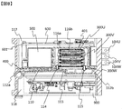
- FIG. 8 is a cross-sectional view of the B surface of the power conversion apparatus 100 shown in FIG. 1 as viewed from the direction of the arrow B without the cover 107 and the cover 108.
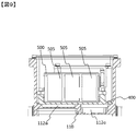
- FIG. 9 is a cross-sectional view of the power conversion device 100 shown in FIG. 1 as viewed from the direction of the arrow on the C surface with the cover 107 and the cover 108 removed.
- the first base plate 400 on which the power semiconductor module 300 ⁇ / b> U and the like are mounted is disposed on the first flow path forming body 110 and connected to the first flow path forming body 110.
- the first base plate 400 is configured to block the opening connected to the flow path 112a, the opening connected to the flow path 112b, and the opening connected to the flow path 112c. Fixed to. Thereby, the first base plate 400 comes into direct contact with the cooling refrigerant.
- the cooling refrigerant flows through the flow path 112 a and into the storage space 402 of the second flow path forming body 401 as indicated by the refrigerant flow 114.
- the cooling refrigerant cools the power semiconductor modules 300U to 300W, and then flows from the storage space 402 to the flow path 112b as indicated by the refrigerant flow 115.
- the power semiconductor modules 300 ⁇ / b> U to 300 ⁇ / b> W include a cooling unit that is housed in the storage space 402 and an electrical connection portion that protrudes outside the storage space 402.
- the protruding direction of the electrical connection portion is the main factor that determines the dimensions of the power semiconductor modules 300U to 300W. For this reason, in order to make the height direction of the power converter device 100 small, it is necessary to fully consider the direction of the power semiconductor module. Further, when the power conversion device 100 is assembled, a power semiconductor module and other components are assembled from the opening of the case 101 of the power conversion device 100 and work such as screw tightening / welding / soldering is performed. It is difficult to work at a deep position (position close to the bottom surface of the case 101).
- the first flow path molded body 110 and the second flow path molded body 401 are configured separately, and the second flow path molded body 401 is connected to the first base plate 400. Further, the second flow path molded body 401 incorporates main electric components such as the power semiconductor modules 300U to 300W into the first base plate 400, and the connection work is performed outside the case 101, not inside the case 101. Then, the first base plate 400 in which the main electrical components are incorporated is fixed to the second flow path molded body 401. Thereby, since there is no outer wall of the power converter 100, that is, the wall of the case 101 at the time of assembly, the direction of work is lost, and the degree of freedom in design and assembly is improved.
- the protruding direction of the electrical connection portion of the power semiconductor modules 300U to 300W is directed to the inner wall of the case 101.
- the capacitor module 500 is built in, and electrical parts such as screw tightening, welding, and soldering are fastened and the capacitor module 500 itself is fixed. However, it is difficult to work deeply from the opening of the case 101. ing.
- the capacitor module 500 is disposed on the first base plate 400.
- the capacitor element 505 shown in FIG. 9 may receive heat from the high-power power semiconductor module via the capacitor side terminal 504, thereby causing a decrease in the performance of the capacitor element 505.
- the second flow path forming body 110 is formed up to a position where the flow path 112a and the flow path 112c face the capacitor module 500. Thereby, the capacitor module 500 can be cooled, and the desired performance and life of the capacitor element 505 can be improved.
- the capacitor module 500 includes a capacitor case 506 that houses a part of the capacitor side terminal 504 and the capacitor element 505.
- the capacitor case 506 is formed with a capacitor side opening 507 from which the capacitor side terminal 505 protrudes. Further, the capacitor case 506 is disposed on the first base plate 400 such that the capacitor side opening 507 faces the first flow path forming body 110 that houses the power semiconductor module.
- the wiring distance of the capacitor side terminal 505 connected to the power semiconductor module can be shortened, and the inductance can be reduced and the heat generation of the capacitor side terminal 505 itself can be suppressed.
- the power semiconductor module 300V is disposed at a position facing the first base plate 400 with the power semiconductor module 300W interposed therebetween, and a cooling refrigerant is interposed between the power semiconductor module 300V and the second power semiconductor module 300W.
- a flow path space 116a is formed to flow the air.
- the power semiconductor module 300U is disposed at a position facing the first base plate 400 with the power semiconductor module 300V and the power semiconductor module 300W interposed therebetween, and is cooled between the power semiconductor module 300U and the second power semiconductor module 300V.
- a flow path space 116b for flowing the refrigerant is formed.
- the coolant can be brought into direct contact with the power semiconductor modules 300U to 300W, and since the coolant flows on both surfaces of each power semiconductor module, the cooling performance of the power semiconductor modules 300U to 300W can be improved.
- the case 101 is divided into a first storage space 117 and a second storage space 118 by the first flow path forming body 110.
- the first base plate 400 on which the main electrical components are mounted is stored in the first storage space 117, while the circuit components constituting the DCDC converter 900 are stored in the second storage space 118 and the first flow path.
- the inverter circuit is cooled by one surface of the first flow path forming body 110
- the DCDC converter is cooled by one surface of the first flow path forming body 110
- the cooling area of the first flow path forming body 110 is reduced. It can be used effectively and leads to the miniaturization of the entire apparatus.
- the second base plate 601 made of metal is disposed at a position facing the first base 400 with the power semiconductor modules 300U to 300W interposed therebetween. Further, the second base plate 601 has a fixing portion 601 ⁇ / b> C connected to the metal case 101.
- the control circuit board 600 is disposed at a position facing the power semiconductor modules 300U to 300W with the second base plate 601 interposed therebetween. Accordingly, the second base plate 601 can shield electromagnetic noise radiated from the power semiconductor modules 300U to 300W, and protect the control circuit board 600 from electromagnetic noise.
- DESCRIPTION OF SYMBOLS 100 Power converter, 101 ... Case, 101A ... Case side surface, 101B ... Case side surface, 101C ... Case side surface, 102 ... Inlet piping, 103 ... Outlet piping, 104U ... AC bus bar, 104V ... AC bus bar, 104W ... AC bus bar, 105 ... opening, 106 ... opening, 107 ... cover, 108 ... cover, 109 ... first insertion port, 110 ... first flow path forming body, 111 ... cover, 112a ... flow path, 112b ... flow path, 112c ... Flow path, 113 ... partition wall, 114 ... flow of refrigerant, 115 ...
- capacitor side terminal 505 ... capacitor element, 506 ... capacitor case, 507 ... capacitor side opening , 600 ... control circuit board, 601A ... fixed part, 601B ... fixed part, 601C ... fixed part, 601 ... second base plate, 602 ... third base plate, 603 ... opening, 900 ... DCDC converter
Landscapes
- Engineering & Computer Science (AREA)
- Microelectronics & Electronic Packaging (AREA)
- Physics & Mathematics (AREA)
- Thermal Sciences (AREA)
- Power Engineering (AREA)
- Inverter Devices (AREA)
- Cooling Or The Like Of Semiconductors Or Solid State Devices (AREA)
Abstract
Description
特許文献1には、パワー半導体モジュール及びコンデンサモジュールを電力変換装置に組み込んだ後に、パワー半導体モジュールの端子とコンデンサモジュールの端子を溶接により接続したり、ドライバ回路基板とパワー半導体モジュールとを半田材により接続するとが記載されている。
図1は、本実施形態に係る電力変換装置100の外観斜視図である。
図2は、本実施形態に係る電力変換装置100の分解斜視図である。第1流路形成体110は、ケース101の高さ方向における真ん中周辺に配置される。第1流路形成体110は、入口配管102及び出口配管103と接続される。
第1流路形成体110とカバー107との間には、第1ベース板400と第2流路形成体401とパワー半導体モジュール300Uないし300Wとコンデンサモジュール500と駆動回路基板200と制御回路基板600等が配置される。
後述されるパワー半導体モジュール300Uないし300Wは、直流電流を交流電流に変換する。後述されるコンデンサモジュール500は、直流電圧を平滑化する。駆動回路基板200は、パワー半導体モジュール300Uないし300Wを駆動する駆動信号を出力する駆動回路を搭載する。制御回路基板600は、駆動回路基板200にパワー半導体モジュール300Uないし300Wを制御するための制御信号を出力する制御回路を搭載する。これらの回路システムの一例は、特開2011-217550号公報に記載されている。
そこで、第1流路成形体110と第2流路成形体401が分離して構成され、第2流路成形体401が第1ベース板400と接続される。さらに第2流路成形体401が第1ベース板400に、パワー半導体モジュール300Uないし300W等の主要電気部品を組み込み、接続作業をケース101内ではなく、ケース101の外で行なう。そして、主要電気部品が組み込まれた第1ベース板400を第2流路成形体401に固定する。これにより、組立時、電力変換装置100の外壁、つまりケース101の壁がない為、作業の方向性が無くなり、設計および組立て性の自由度が向上する。また、パワー半導体モジュール300Uないし300Wの電気的接続の方向も自由度が向上するため、パワー半導体モジュール300Uないし300Wは、パワー半導体モジュール300Uないし300Wの電気接続部の突出方向がケース101の内壁に向かうように配置することができる。これにより、電力変換装置100の高さ方向を小さくすることができるようになる。
Claims (9)
- 直流電流を交流電流に変換するパワー半導体素子を有するパワー半導体モジュールと、
冷却冷媒を流す第1流路を形成する第1流路形成体と、
冷却冷媒を流す第2流路を形成する第2流路形成体と、
前記第2流路形成体を搭載する第1ベース板と、
前記パワー半導体素子を駆動する駆動信号を出力する駆動回路を搭載した駆動回路基板と、
前記パワー半導体モジュールと前記第1流路形成体と前記第2流路形成体と前記第1ベース板と前記駆動回路基板を収納するケースと、を備え、
前記駆動回路基板は、前記駆動回路の搭載面が前記第2流路形成体の側壁と対向するように配置され、
前記第2流路形成体は、前記パワー半導体モジュールを収納する収納空間を形成し、
さらに前記第2流路形成体は、前記収納空間と繋がる挿入口を前記駆動回路の搭載面と対向する前記側壁に形成し、
前記パワー半導体モジュールは、前記挿入口を通って前記駆動回路基板と接続される制御端子を有し、
前記第1流路形成体は、前記ケースに固定され、
さらに前記第1流路形成体は、前記第1流路と繋がる開口部を形成し、
前記第1ベース板は、前記開口部を塞ぐとともに前記第1流路形成体に接続され、
さらに前記第1ベース板は、前記第1流路と前記第2流路を繋ぐ第1貫通孔を形成する電力変換装置。 - 請求項1に記載された電力変換装置であって、
直流電圧を平滑化するコンデンサモジュールと、を備え、
前記コンデンサモジュールは、前記第1ベース板上に配置される電力変換装置。 - 請求項2に記載された電力変換装置であって、
前記第1流路は、前記コンデンサモジュールと対向する位置まで形成される電力変換装置。 - 請求項2又は3に記載されたいずれかの電力変換装置であって、
前記コンデンサモジュールは、コンデンサ素子と、前記コンデンサ素子と電気的に接続されるコンデンサ側端子と、前記コンデンサ素子と前記コンデンサ側端子を収納するコンデンサケースと、を有し、
前記コンデンサケースは、前記コンデンサ側端子が突出するコンデンサ側開口部を形成し、
さらに前記コンデンサケースは、前記コンデンサ側開口部が前記第2流路形成体と対向するように前記第1ベース板に配置される電力変換装置。 - 請求項1ないし4に記載されたいずれかの電力変換装置であって、
前記パワー半導体モジュールは、第1パワー半導体モジュールと第2パワー半導体モジュールとにより構成され、
前記第2パワー半導体モジュールは、前記第1パワー半導体モジュールを挟んで前記第1ベース板と対向する位置に配置され、
前記第1パワー半導体モジュールと前記第2パワー半導体モジュールとの間に前記冷却冷媒を流す流路空間が形成される電力変換装置。 - 請求項1ないし5に記載されたいずれかの電力変換装置であって、
前記第1ベース板に、前記第1流路と前記第2流路を繋ぐ第2貫通孔を形成され、
前記第1流路形成体は、前記第1ベース板と接触するとともに前記第1貫通孔と前記第2貫通孔との間に配置される隔壁を有する電力変換装置。 - 請求項1ないし4に記載されたいずれかの電力変換装置であって、
直流電圧を変換するDCDCコンバータ回路を備え、
前記ケースは、前記第1流路形成体によって第1収納空間と第2収納空間に分けられ、
前記パワー半導体モジュールと前記第2流路形成体と前記第1ベース板は、前記第1収納空間に収納され、
前記DCDCコンバータ回路は、前記第2収納空間に収納されるとともに前記第2流路形成体に配置される電力変換装置。 - 請求項1ないし7に記載されたいずれかの電力変換装置であって、
前記パワー半導体モジュールを挟んで前記第1ベースと対向する位置に配置されるとともに前記ケースに固定される金属製の第2ベース板と、
前記駆動回路に前記パワー半導体素子を制御するための制御信号を出力する制御回路を搭載した制御回路基板と、を備え、
前記制御回路基板は、前記第2ベース板を挟んで前記パワー半導体モジュールと対向する位置に配置される電力変換装置。 - 請求項1ないし8に記載されたいずれかの電力変換装置であって、
前記第1流路形成体は、前記ケースと一体に形成される電力変換装置。
Priority Applications (3)
| Application Number | Priority Date | Filing Date | Title |
|---|---|---|---|
| US14/419,997 US20150163961A1 (en) | 2012-09-28 | 2013-07-24 | Power Conversion Apparatus |
| CN201380041069.2A CN104584408B (zh) | 2012-09-28 | 2013-07-24 | 电力转换装置 |
| DE112013004779.9T DE112013004779B4 (de) | 2012-09-28 | 2013-07-24 | Stromrichtvorrichtung |
Applications Claiming Priority (2)
| Application Number | Priority Date | Filing Date | Title |
|---|---|---|---|
| JP2012-215456 | 2012-09-28 | ||
| JP2012215456A JP5753829B2 (ja) | 2012-09-28 | 2012-09-28 | 電力変換装置 |
Publications (1)
| Publication Number | Publication Date |
|---|---|
| WO2014050276A1 true WO2014050276A1 (ja) | 2014-04-03 |
Family
ID=50387690
Family Applications (1)
| Application Number | Title | Priority Date | Filing Date |
|---|---|---|---|
| PCT/JP2013/069971 Ceased WO2014050276A1 (ja) | 2012-09-28 | 2013-07-24 | 電力変換装置 |
Country Status (5)
| Country | Link |
|---|---|
| US (1) | US20150163961A1 (ja) |
| JP (1) | JP5753829B2 (ja) |
| CN (1) | CN104584408B (ja) |
| DE (1) | DE112013004779B4 (ja) |
| WO (1) | WO2014050276A1 (ja) |
Cited By (2)
| Publication number | Priority date | Publication date | Assignee | Title |
|---|---|---|---|---|
| CN105459077A (zh) * | 2014-09-30 | 2016-04-06 | 精工爱普生株式会社 | 机器人 |
| CN106664030A (zh) * | 2014-07-29 | 2017-05-10 | 日立汽车系统株式会社 | 电力变换装置 |
Families Citing this family (15)
| Publication number | Priority date | Publication date | Assignee | Title |
|---|---|---|---|---|
| JP5563383B2 (ja) * | 2010-06-21 | 2014-07-30 | 日立オートモティブシステムズ株式会社 | 電力変換装置 |
| JP5738817B2 (ja) * | 2012-09-14 | 2015-06-24 | 日立オートモティブシステムズ株式会社 | 電力変換装置 |
| KR102458738B1 (ko) * | 2015-11-11 | 2022-10-25 | 현대모비스 주식회사 | 커패시터 직접냉각방식의 인버터 |
| KR102361530B1 (ko) * | 2015-11-11 | 2022-02-09 | 현대모비스 주식회사 | 캐패시터 직접냉각방식의 인버터 |
| KR101821878B1 (ko) * | 2016-02-24 | 2018-01-24 | 엘에스산전 주식회사 | 인버터 |
| WO2018055668A1 (ja) * | 2016-09-20 | 2018-03-29 | 三菱電機株式会社 | 電力変換装置 |
| CN106696858A (zh) * | 2016-12-23 | 2017-05-24 | 中国第汽车股份有限公司 | 一种电动汽车高压功率电子装置布置结构 |
| US11011996B2 (en) | 2017-03-30 | 2021-05-18 | Hitachi Automotive Systems, Ltd. | Power converter |
| CN112313870B (zh) * | 2018-06-22 | 2023-12-01 | 日立安斯泰莫株式会社 | 电力转换装置 |
| DE112019002805B4 (de) * | 2018-07-04 | 2026-01-08 | Hitachi Astemo, Ltd. | Leistungsumwandlungsvorrichtung |
| JP7239380B2 (ja) * | 2019-04-16 | 2023-03-14 | 株式会社日立製作所 | 電力変換装置 |
| CN113853737B (zh) * | 2019-05-27 | 2025-07-15 | 三菱电机株式会社 | 电力转换装置及电力转换装置的制造方法 |
| JP7424125B2 (ja) * | 2020-03-12 | 2024-01-30 | ニデック株式会社 | インバータ装置 |
| JP7526630B2 (ja) * | 2020-10-01 | 2024-08-01 | 株式会社日立製作所 | パワー半導体装置 |
| CN113692155A (zh) * | 2021-08-03 | 2021-11-23 | 深圳麦格米特电气股份有限公司 | 一种电源及用电设备 |
Citations (2)
| Publication number | Priority date | Publication date | Assignee | Title |
|---|---|---|---|---|
| JP2008118753A (ja) * | 2006-11-02 | 2008-05-22 | Hitachi Ltd | 電力変換装置 |
| JP2011217550A (ja) * | 2010-04-01 | 2011-10-27 | Hitachi Automotive Systems Ltd | 電力変換装置 |
Family Cites Families (19)
| Publication number | Priority date | Publication date | Assignee | Title |
|---|---|---|---|---|
| US6972957B2 (en) * | 2002-01-16 | 2005-12-06 | Rockwell Automation Technologies, Inc. | Modular power converter having fluid cooled support |
| EP2216891B1 (en) * | 2003-08-21 | 2012-01-04 | Denso Corporation | Mounting structure ofa semiconductor device |
| JP2005117829A (ja) * | 2003-10-09 | 2005-04-28 | Toshiba Corp | 液冷式電力変換装置 |
| JP4756935B2 (ja) * | 2005-06-29 | 2011-08-24 | 本田技研工業株式会社 | コンデンサ搭載型インバータユニット |
| JP4848187B2 (ja) * | 2006-01-17 | 2011-12-28 | 日立オートモティブシステムズ株式会社 | 電力変換装置 |
| JP4857017B2 (ja) * | 2006-04-27 | 2012-01-18 | 日立オートモティブシステムズ株式会社 | 電力変換装置 |
| JP4434181B2 (ja) * | 2006-07-21 | 2010-03-17 | 株式会社日立製作所 | 電力変換装置 |
| JP4567029B2 (ja) * | 2007-06-22 | 2010-10-20 | 日立オートモティブシステムズ株式会社 | 電力変換装置 |
| US7710723B2 (en) * | 2007-07-17 | 2010-05-04 | Gm Global Technology Operations, Inc. | Vehicle inverter assembly with cooling channels |
| JP4580997B2 (ja) * | 2008-03-11 | 2010-11-17 | 日立オートモティブシステムズ株式会社 | 電力変換装置 |
| US7952856B2 (en) * | 2008-06-02 | 2011-05-31 | Honda Motor Co., Ltd. | Power control unit and hybrid vehicle comprising same |
| JP4657329B2 (ja) * | 2008-07-29 | 2011-03-23 | 日立オートモティブシステムズ株式会社 | 電力変換装置および電動車両 |
| JP4708459B2 (ja) * | 2008-07-29 | 2011-06-22 | 日立オートモティブシステムズ株式会社 | 電力変換装置 |
| JP4643695B2 (ja) | 2008-09-02 | 2011-03-02 | 日立コンピュータ機器株式会社 | 双方向dc−dcコンバータ及びその制御方法 |
| US8059404B2 (en) * | 2008-10-09 | 2011-11-15 | GM Global Technology Operations LLC | Power inverters |
| JP5417314B2 (ja) * | 2010-12-27 | 2014-02-12 | 日立オートモティブシステムズ株式会社 | 電力変換装置 |
| JP5506749B2 (ja) * | 2011-07-25 | 2014-05-28 | 日立オートモティブシステムズ株式会社 | 電力変換装置 |
| JP5504219B2 (ja) * | 2011-07-27 | 2014-05-28 | 日立オートモティブシステムズ株式会社 | 電力変換装置 |
| JP5508357B2 (ja) * | 2011-07-29 | 2014-05-28 | 日立オートモティブシステムズ株式会社 | 電力変換装置 |
-
2012
- 2012-09-28 JP JP2012215456A patent/JP5753829B2/ja active Active
-
2013
- 2013-07-24 CN CN201380041069.2A patent/CN104584408B/zh active Active
- 2013-07-24 DE DE112013004779.9T patent/DE112013004779B4/de active Active
- 2013-07-24 US US14/419,997 patent/US20150163961A1/en not_active Abandoned
- 2013-07-24 WO PCT/JP2013/069971 patent/WO2014050276A1/ja not_active Ceased
Patent Citations (2)
| Publication number | Priority date | Publication date | Assignee | Title |
|---|---|---|---|---|
| JP2008118753A (ja) * | 2006-11-02 | 2008-05-22 | Hitachi Ltd | 電力変換装置 |
| JP2011217550A (ja) * | 2010-04-01 | 2011-10-27 | Hitachi Automotive Systems Ltd | 電力変換装置 |
Cited By (3)
| Publication number | Priority date | Publication date | Assignee | Title |
|---|---|---|---|---|
| CN106664030A (zh) * | 2014-07-29 | 2017-05-10 | 日立汽车系统株式会社 | 电力变换装置 |
| CN106664030B (zh) * | 2014-07-29 | 2018-10-30 | 日立汽车系统株式会社 | 电力变换装置 |
| CN105459077A (zh) * | 2014-09-30 | 2016-04-06 | 精工爱普生株式会社 | 机器人 |
Also Published As
| Publication number | Publication date |
|---|---|
| DE112013004779T5 (de) | 2015-06-11 |
| CN104584408B (zh) | 2018-03-30 |
| CN104584408A (zh) | 2015-04-29 |
| DE112013004779B4 (de) | 2026-05-07 |
| JP5753829B2 (ja) | 2015-07-22 |
| US20150163961A1 (en) | 2015-06-11 |
| JP2014072938A (ja) | 2014-04-21 |
Similar Documents
| Publication | Publication Date | Title |
|---|---|---|
| JP5753829B2 (ja) | 電力変換装置 | |
| JP5914290B2 (ja) | 電力変換装置 | |
| KR102131684B1 (ko) | 차량 탑재용 전력 변환 장치 | |
| US10128770B2 (en) | Converter and electric power conversion apparatus | |
| JP5725067B2 (ja) | 電力変換装置 | |
| US9750147B2 (en) | Power converter | |
| JP5024169B2 (ja) | 電力変換装置 | |
| JP5529477B2 (ja) | インバータ一体型電動圧縮機 | |
| JP2014090538A (ja) | 電力変換装置 | |
| CN102948064A (zh) | 电力转换装置 | |
| JP2011182631A (ja) | 電力変換装置 | |
| US20180041136A1 (en) | Power Semiconductor Module and Electric Power Conversion Device | |
| JP6169181B2 (ja) | Dc−dcコンバータ装置 | |
| CN115224955B (zh) | 功率转换装置 | |
| JP2010087002A (ja) | 発熱部品冷却構造 | |
| JP5488502B2 (ja) | 電力変換装置 | |
| US10461656B2 (en) | Power conversion device having a cover that covers DC positive and negative terminals | |
| JP5494421B2 (ja) | 電力変換装置 | |
| JP6115430B2 (ja) | 電力変換装置 | |
| JP2008131792A (ja) | インバータ一体型電動圧縮機 | |
| JP5644643B2 (ja) | 負荷駆動装置 | |
| JP6364384B2 (ja) | 電力変換装置 | |
| JP2018148794A (ja) | 電力変換装置 | |
| JP6314784B2 (ja) | 電力変換装置 | |
| JP2017139963A (ja) | 電力変換装置 |
Legal Events
| Date | Code | Title | Description |
|---|---|---|---|
| 121 | Ep: the epo has been informed by wipo that ep was designated in this application |
Ref document number: 13841707 Country of ref document: EP Kind code of ref document: A1 |
|
| WWE | Wipo information: entry into national phase |
Ref document number: 14419997 Country of ref document: US |
|
| WWE | Wipo information: entry into national phase |
Ref document number: 1120130047799 Country of ref document: DE Ref document number: 112013004779 Country of ref document: DE |
|
| 122 | Ep: pct application non-entry in european phase |
Ref document number: 13841707 Country of ref document: EP Kind code of ref document: A1 |
|
| WWG | Wipo information: grant in national office |
Ref document number: 112013004779 Country of ref document: DE |