WO2014050133A1 - 光電場増強デバイスとその製造方法、及びそれを用いた測定装置 - Google Patents
光電場増強デバイスとその製造方法、及びそれを用いた測定装置 Download PDFInfo
- Publication number
- WO2014050133A1 WO2014050133A1 PCT/JP2013/005755 JP2013005755W WO2014050133A1 WO 2014050133 A1 WO2014050133 A1 WO 2014050133A1 JP 2013005755 W JP2013005755 W JP 2013005755W WO 2014050133 A1 WO2014050133 A1 WO 2014050133A1
- Authority
- WO
- WIPO (PCT)
- Prior art keywords
- photoelectric field
- marker pattern
- excitation light
- image
- light
- Prior art date
- Legal status (The legal status is an assumption and is not a legal conclusion. Google has not performed a legal analysis and makes no representation as to the accuracy of the status listed.)
- Ceased
Links
Images



Classifications
-
- G—PHYSICS
- G01—MEASURING; TESTING
- G01N—INVESTIGATING OR ANALYSING MATERIALS BY DETERMINING THEIR CHEMICAL OR PHYSICAL PROPERTIES
- G01N21/00—Investigating or analysing materials by the use of optical means, i.e. using sub-millimetre waves, infrared, visible or ultraviolet light
- G01N21/62—Systems in which the material investigated is excited whereby it emits light or causes a change in wavelength of the incident light
- G01N21/63—Systems in which the material investigated is excited whereby it emits light or causes a change in wavelength of the incident light optically excited
- G01N21/65—Raman scattering
- G01N21/658—Raman scattering enhancement Raman, e.g. surface plasmons
-
- G—PHYSICS
- G01—MEASURING; TESTING
- G01N—INVESTIGATING OR ANALYSING MATERIALS BY DETERMINING THEIR CHEMICAL OR PHYSICAL PROPERTIES
- G01N21/00—Investigating or analysing materials by the use of optical means, i.e. using sub-millimetre waves, infrared, visible or ultraviolet light
- G01N21/01—Arrangements or apparatus for facilitating the optical investigation
-
- G—PHYSICS
- G01—MEASURING; TESTING
- G01N—INVESTIGATING OR ANALYSING MATERIALS BY DETERMINING THEIR CHEMICAL OR PHYSICAL PROPERTIES
- G01N21/00—Investigating or analysing materials by the use of optical means, i.e. using sub-millimetre waves, infrared, visible or ultraviolet light
- G01N21/62—Systems in which the material investigated is excited whereby it emits light or causes a change in wavelength of the incident light
- G01N21/63—Systems in which the material investigated is excited whereby it emits light or causes a change in wavelength of the incident light optically excited
- G01N21/64—Fluorescence; Phosphorescence
- G01N21/6402—Atomic fluorescence; Laser induced fluorescence
-
- G—PHYSICS
- G01—MEASURING; TESTING
- G01N—INVESTIGATING OR ANALYSING MATERIALS BY DETERMINING THEIR CHEMICAL OR PHYSICAL PROPERTIES
- G01N2201/00—Features of devices classified in G01N21/00
- G01N2201/02—Mechanical
-
- G—PHYSICS
- G01—MEASURING; TESTING
- G01N—INVESTIGATING OR ANALYSING MATERIALS BY DETERMINING THEIR CHEMICAL OR PHYSICAL PROPERTIES
- G01N2201/00—Features of devices classified in G01N21/00
- G01N2201/06—Illumination; Optics
- G01N2201/061—Sources
- G01N2201/06113—Coherent sources; lasers
Definitions
- FIG. 1A is a schematic top view of a photoelectric field enhancement device 1 according to an embodiment of the present invention
- FIG. 1B is a schematic cross-sectional view in the thickness direction.
- the photoelectric field enhancement device 1 performs two-dimensional scanning in the main scanning direction and the sub-scanning direction on the surface 40s on which the sample is placed, and outputs each signal light from each scanning point.
- FIG. 1B localized plasmons are induced on the surface 40s by the irradiation of the excitation light L1, and the surface 40s is irradiated by the irradiation of the excitation light L1, as shown in FIG. 1B.
- the intensity of the signal light L2 emitted from the sample placed on is increased.
- the transparent substrate 10 may have a single layer structure or a laminated structure.
- the laminated substrate include those obtained by forming a TiO 2 film as a protective film on a glass substrate.
- the marker pattern 20 is not particularly limited as long as it can generate a signal light L2 by irradiation of the excitation light L1 and can acquire a two-dimensional signal image by an image acquisition unit described later.
- the marker pattern 20 has a reflectance with respect to the excitation light L1. Examples thereof include a high material, a material having a high absorption rate for the excitation light L1, and a material that emits fluorescence when irradiated with the excitation light L1.
- fluorescence is not easily cut by a wavelength selection filter arranged before reaching the detector, it can be used as a marker formed only in a specific region.
- the marker pattern 20 preferably has a thickness of 50 nm or more so that signal light can be detected with high sensitivity.
- the fine concavo-convex structure 40 made of a metal film is not particularly limited as long as the average size and average pitch of the concavo-convex convex portions can cause localized plasmons on the surface by irradiation with the excitation light L1, It is preferably shorter than the wavelength of the excitation light L1.
- the fine concavo-convex structure 40 made of a metal film preferably has an average depth of 200 nm or less from the top of the convex portion to the bottom of the adjacent concave portion, and an average pitch between the vertices of the nearest convex portions separating the concave portions of 200 nm or less.
- the fine concavo-convex structure 40 made of a metal film may be provided with the fine concavo-convex structure 30 on the base substrate as in this embodiment, and may have a fine concavo-convex structure corresponding to the concavo-convex structure of the base.
- a substrate having a high surface smoothness may be used, and a substrate having a fine concavo-convex structure independent of the shape of the surface of the base substrate may be used.
- the metal does not always have the same shape as the base because it easily aggregates.
- the marker pattern 20 is preferably formed on a fine concavo-convex structure 40 made of a metal film.
- the patterning of this marker is difficult to manufacture because it easily causes cracks in the fine concavo-convex structure. According to the configuration of the present embodiment, it is possible to form a marker pattern having a precise shape without affecting the fine concavo-convex structure.
- the marker pattern 20 is directly formed on the substrate 10.
- the surface 40s of the fine concavo-convex structure 40 made of a metal film must exist within the depth of focus of the optical system that detects the signal light.
- a depth of focus is about 700 nm in a system that uses a 780 nm laser as excitation light and detects from a transparent substrate 10 side with a microscope lens having a magnification of 100 times and a numerical aperture of 0.9. is there.
- the total film thickness of the transparent fine concavo-convex structure 30 and the fine concavo-convex structure 40 made of a metal film is 700 nm or less as long as the film can provide a sufficient electric field enhancing effect.
- the average film thickness of the fine concavo-convex structure 40 made of a metal film is preferably in the range of 10 to 100 nm so that localized plasmons can be well induced by irradiation with the excitation light L1.
- an aluminum layer 30a is formed on the surface of the transparent substrate 10 and the marker pattern 20 by a sputtering method to a film thickness of about several tens of nm.
- the transparent substrate 10 with the aluminum layer 30a is submerged in boiling pure water, and taken out after a few minutes (about 5 minutes).
- this boiling treatment boiling treatment
- the aluminum layer becomes transparent and a transparent fine uneven structure (boehmite layer) 30 is formed.
- a metal film such as Au is formed by vapor deposition, and the photoelectric field enhancement device 1 having at least the surface of the metal fine concavo-convex structure 40 can be obtained.
- the metal film 40 is not limited to vapor deposition, and may be formed, for example, by immobilizing metal fine particles. Further, the vapor deposition method is not limited to a normal vapor deposition method, and an oblique vapor deposition method may be used.
- the photoelectric field enhancement device can be manufactured as described above.
- the measuring apparatus 100 includes a photoelectric field enhancement device 1 in which the sample S is placed on the surface 40S, and excitation light L1 from the back surface 10s side (transparent substrate 10 side) of the photoelectric field enhancement device 1 to the sample S.
- the detection means 120 for detecting the signal light L2 from each scanning point from the back surface 10s side, and the signal light L2 from the scanning point detected by the detection means 120 Based on the detection means 120 for detecting the signal light L2 from each scanning point from the back surface 10s side, and the signal light L2 from the scanning point detected by the detection means 120, a two-dimensional signal image and a marker pattern image on the front surface 40s.
- the photoelectric field enhancement device 1 is configured so that the distance between the marker pattern forming surface of the transparent substrate 10 and the fine concavo-convex structure surface 40s is within the depth of focus of the detection means. Designed.
- the excitation light irradiation means 110 transmits an excitation light source 111 that emits the excitation light L1 and the excitation light L1 to the substrate 10 side, and the signal light L2 that is generated from the subject in the sample S and is enhanced by the irradiation of the excitation light L1.
- the dichroic mirror 112 that reflects the light from the substrate 10 side including the light to the light detection unit 120 side, and the excitation light L1 that has passed through the dichroic mirror 112 is condensed on the region where the sample S of the photoelectric field enhancement device 1 is placed.
- a lens 113 that collimates the light from the sample side is also provided.
- the excitation light irradiation means 110 may be provided with a laser line filter or the like that uses the light L1 emitted from the excitation light source 111 as excitation light of a specific wavelength, if necessary.
- Detection by the light detector 120 is performed at each scanning point scanned in the main scanning direction and the sub-scanning direction shown in FIG. 1 by the scanning unit 140 and arranged at a predetermined interval, and detected at each scanning point. Detection results such as the intensity and spectrum of the signal light L2 are sent to the image acquisition means 130.
- the image acquisition unit 130 acquires a two-dimensional signal image and a marker pattern image on the surface 40 s based on the detection result of each scanning point. For example, when the obtained detection result is a spectral result such as a Raman spectrum, a desired wavelength is determined from the obtained spectral pattern, and the obtained signal is located at a position corresponding to each scanning point on the surface 40s. By displaying, the detection result of the Raman spectrum can be visualized and two-dimensional imaging can be performed.
- a spectral result such as a Raman spectrum
- the two-dimensional image obtained at this stage is an image including jitter shift.
- a two-dimensional image of the marker pattern 20 is obtained together with a two-dimensional image of the sample.
- a schematic diagram of an image obtained by the image acquisition means 130 of the measuring apparatus 100 is shown on the left side of FIG.
- the two-dimensional signal image corrected by the image correction means 150 is sent to the display means 160 for displaying it and displayed as a correct two-dimensional signal image as shown in the right figure of FIG.
- the photoelectric field enhancing device 1 and the measuring apparatus 100 using the same can be suitably used for chemical imaging such as Raman scattered light, fluorescence, higher harmonics, Rayleigh scattered light, or Mie scattered light.
- the photoelectric field enhancement device 1 is formed on the transparent substrate 10, the marker pattern 20 that is directly formed on the transparent substrate 10, and extends in a direction not parallel to the main scanning direction in two-dimensional scanning, the marker pattern 20, and the transparent substrate 10.
- at least the surface 40 s has a fine concavo-convex structure (30, 40) made of the metal film 40.
- the photoelectric field enhancement device 1 is made of a material transparent to the excitation light L1 and the signal light L2, the detection of the signal light L2 of the sample and the detection of the marker pattern 20 are performed on the back surface of the photoelectric field enhancement device. It can be carried out from the 10s side (the side opposite to the sample contact surface). Therefore, according to the present invention, a high-accuracy signal image can be acquired without requiring precise machine control, and chemical imaging is performed at a high S / N even for a sample of ⁇ m order or more such as a cell. be able to.
- the excitation light irradiation means 110 was arrange
- positioning surface side) of the photoelectric field enhancement device 1 and irradiating excitation light from the surface side.
- the fine metal concavo-convex structure of the photoelectric field enhancement device localized plasmon resonance can be similarly induced regardless of whether excitation light is incident from either of the front and back sides, and a photoelectric field enhancement effect can be obtained.
Landscapes
- Health & Medical Sciences (AREA)
- Physics & Mathematics (AREA)
- Biochemistry (AREA)
- Life Sciences & Earth Sciences (AREA)
- Chemical & Material Sciences (AREA)
- Analytical Chemistry (AREA)
- General Health & Medical Sciences (AREA)
- General Physics & Mathematics (AREA)
- Immunology (AREA)
- Pathology (AREA)
- Nuclear Medicine, Radiotherapy & Molecular Imaging (AREA)
- Optics & Photonics (AREA)
- Investigating, Analyzing Materials By Fluorescence Or Luminescence (AREA)
- Investigating Or Analysing Materials By Optical Means (AREA)
Description
本発明は、局在プラズモンを誘起しうる微細な金属凹凸構造を備えた光電場増強デバイスとその製造方法、及び、この光電場増強デバイスを用いて増強された信号光を検出してその物理特性を測定する測定装置に関するものである。
金属表面における局在プラズモン共鳴現象による電場増強効果を利用した光電場増強デバイスが知られている。かかる光電場増強デバイスは、金属体、特に表面にナノオーダの凹凸を有する金属体に試料を接触させた状態で光を照射すると、その表面に局在プラズモン共鳴による増強電場を生じることから、光の照射により被検体から発せられる信号光の光特性に基づいて被検体の同定や定量を行う測定装置において、被検体を担持する担体(基板)として適用することにより、信号光を増強電場により増強させて高感度な測定を可能にする。
光電場増強デバイスを利用した測定方法として、表面増強ラマン(SERS)分光法が良く知られている(非特許文献1参照)。ラマン分光法は、物質に単波長光を照射して得られる散乱光を分光して、ラマン散乱光のスペクトル(ラマンスペクトル)を得る方法であり、ラマンシフトの検出による物質の同定や、ラマンスペクトル強度による試料中の被検体濃度の測定等に使用されている。
光電場増強デバイスとしては、Si基板の表面に凹凸を設け、その凹凸面に金属膜を形成した基板が主に用いられている(特許文献1~3参照)。
また、Al基板の表面を陽極酸化して一部を金属酸化物層(Al2O3)とし、陽極酸化の過程で金属酸化物層内部に自然形成され、金属酸化物層の表面において開口した複数の微細孔内に、金属が充填された基板も提案されている(特許文献4参照)。
また、細胞などのμmオーダー以上の試料であっても、試料自身が信号光に対する遮蔽体ならずに良好なS/Nで増強された信号光を検出可能にする光電場増強デバイスとして、本発明者らは、ベーマイトと呼ばれる透明微細凹凸構造の凹凸表面を、金属膜で覆った光電場増強デバイスを開示している(特許文献5,6)。
かかる光電場増強デバイスによれば、デバイスの裏面側(試料担持面と反対側)から増強された信号光を検出することができるため、被検体により遮蔽されることなく増強光電場により増強された信号光を検出することができる。
一方、担体上の試料を決まったポイント間隔(空間分解能)で走査して多点測定を行い、測定結果を可視化して面分布画像(マップ)を表示するケミカルイメージング技術がある。ケミカルイメージングによれば、試料の面内における成分分布等を直感的に把握することができる。特許文献7,8にはラマンスペクトルイメージングが開示されている。
Optics Express Vol.17, No.2118556
ケミカルイメージングにおいては、2次元走査による多点測定を行うが、2次元走査において、副走査方向のスタートラインが装置のクロック等の影響(ジッタ)によって揃わなくなる現象を生じるため、精度の高い信号画像を取得するためにジッタの補正(除去)を行う必要がある。ジッタ補正は、精密な機械制御を行うことが一般的であるが、精密な機械制御には高価な制御装置が必要となることから、低コスト化が望まれている。
本発明は上記事情に鑑みてなされたものであり、精密な機械制御を要することなく精度の高い信号画像を取得可能なケミカルイメージングが可能であり、細胞などのμmオーダー以上の試料であっても高いS/Nにて測定が可能な測定装置及びそれを可能にする光電場増強デバイスを提供することを目的とするものである。
本発明の光電場増強デバイスは、励起光の照射により表面に局在プラズモンが誘起され、励起光の照射により表面に載置された試料から発せられる信号光の強度を増強する光電場増強デバイスであって、その表面に対して、励起光を表面内方向に2次元走査して、各走査点からの各信号光を裏面側から検出し、検出により得られた各信号光に基づいて表面における2次元信号画像を取得する測定方法に用いられるものであり、
透明基板と、透明基板上に直接形成され、2次元走査における主走査方向と非平行方向に延びるマーカーパターンと、マーカーパターン及び透明基板上に形成された少なくとも表面が金属膜からなる微細凹凸構造を備えたことを特徴とするものである。
透明基板と、透明基板上に直接形成され、2次元走査における主走査方向と非平行方向に延びるマーカーパターンと、マーカーパターン及び透明基板上に形成された少なくとも表面が金属膜からなる微細凹凸構造を備えたことを特徴とするものである。
ここで、透明とは、励起光、および該光により被検体から生じる光に対し、透過率が50%以上であることをいうものとする。なお、これらの光に対して、透過率は75%以上、さらには90%以上であることが好ましい。
少なくとも表面を覆う金属微細構造の下層の透明下地基材は、下地基材に照射される励起光、および励起光により被検体から生じる光に対し、透過率が50%以上であるものとする。なお、これらの光に対して、透過率は75%以上、さらには90%以上であることが好ましい。
ここで「載置された試料」とは、具体的にはデバイス表面に接触あるいは隣接している試料や、デバイス表面に近接して存在する試料等である。
微細凹凸構造は、バイヤーライト又はベーマイトからなる透明微細凹凸構造の凹凸面に金属膜が成膜されてなるものであることが好ましい。
マーカーパターンの好適な態様としては、主走査方向と略垂直に交わるライン状のパターンが挙げられる。
マーカーパターンとしては、Cr,Au,Al,又はAg等の、励起光に対する反射率が高い少なくとも1種の材料から形成されてなる態様、又は、カーボンブラック又は窒化チタン等の、励起光に対する吸収率が高い少なくとも1種の材料により形成されてなる態様、励起光の照射により蛍光を発する材料により形成されてなる態様が挙げられる。
本発明の測定装置は、上記本発明の光電場増強デバイスと、励起光をデバイスの試料が載置される表面に照射する励起光照射手段と、励起光をデバイスの表面内方向に2次元走査させる走査手段と、各走査点からの各信号光を裏面側から検出する検出手段と、検出手段により検出された走査点からの信号光に基づいて、表面における2次元信号画像及びマーカーパターン画像を取得する画像取得手段と、マーカーパターン画像に基づいて、取得された2次元信号画像を補正する画像補正手段と、画像補正手段により補正された2次元信号画像を表示する表示手段を備えたことを特徴としている。
本発明の測定装置において、透明基板のマーカーパターン形成面と、微細凹凸構造表面との距離が、検出手段の焦点深度以内であることが好ましい。
本発明の光電場増強デバイスの製造方法は、透明基板を用意し、透明基板上に、2次元走査における主走査方向と非平行方向に延びるマーカーパターンを直接形成し、このマーカーパターンが形成された透明基板上に、アルミニウムを主成分とする金属膜を形成し、少なくとも該金属膜を浸水させた後に煮沸処理を施すことによりベーマイト層を形成し、ベーマイト層上に金属膜を形成することを特徴とするものである。
マーカーパターンは、リソグラフィにより形成することが好ましい。
本発明の光電場増強デバイスは、透明基板と、透明基板上に直接形成され、2次元走査における主走査方向と非平行方向に延びるマーカーパターンと、マーカーパターン及び透明基板上に形成された少なくとも表面が金属膜からなる微細凹凸構造を備えた構成としている。かかる構成の光電場増強デバイスを用いたケミカルイメージング測定では、励起光照射のジッタに基づく2次元画像のずれを、マーカーパターンの画像のずれ量に基づいて補正することにより補正して精度の高い信号画像を取得することができる。また、光電場増強デバイスが励起光や信号光に対して透明な材料により構成していることから、信号光の検出やマーカーパターンの検出を光電場増強デバイスの裏面側(試料接触面と反対側)から実施することができる。従って、本発明によれば、精密な機械制御を要することなく精度の高い信号画像を取得可能であり、細胞などのμmオーダー以上の試料であっても高いS/Nにてケミカルイメージングを実施することができる。
以下、図面を参照して本発明の測定方法および測定装置の実施形態について説明する。なお、視認しやすくするため、図面中の各構成要素の縮尺等は実際のものとは適宜異ならせてある。
「光電場増強デバイス及びそれを用いた測定装置」
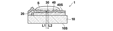
図1Aは、本発明の一実施形態にかかる光電場増強デバイス1の上面概略図、図1Bは厚み方向断面概略図である。
光電場増強デバイス1は、図1Aに示されるように、試料が載置される表面40sに対して、主走査方向と副走査方向に2次元走査して、各走査点からの各信号光に基づいて表面における2次元信号画像を得るイメージングに用いられるものであり、図1Bに示されるように、励起光L1の照射により表面40sに局在プラズモンが誘起され、励起光L1の照射により表面40sに載置された試料から発せられる信号光L2の強度を増強するものである。
図1Aは、本発明の一実施形態にかかる光電場増強デバイス1の上面概略図、図1Bは厚み方向断面概略図である。
光電場増強デバイス1は、図1Aに示されるように、試料が載置される表面40sに対して、主走査方向と副走査方向に2次元走査して、各走査点からの各信号光に基づいて表面における2次元信号画像を得るイメージングに用いられるものであり、図1Bに示されるように、励起光L1の照射により表面40sに局在プラズモンが誘起され、励起光L1の照射により表面40sに載置された試料から発せられる信号光L2の強度を増強するものである。
光電場増強デバイス1は、透明基板10上に、透明基板10上に直接形成されたマーカーパターン20と、透明基板10及びマーカーパターン20上に形成された、透明微細凹凸構造30と、透明微細凹凸構造30上に形成された金属膜からなる微細凹凸構造40とからなり、各走査点からの各信号光L2は、裏面10s側から検出される。
透明基板10は、透明性を有していれば特に制限されないが、透明性が高い方が好ましく、例えばガラスやアクリル樹脂等が挙げられる。透明基板10は単層構造であっても積層構造であってもよい。積層基板は、例えば、ガラス基板上に保護膜としてTiO2膜を形成してなるもの等が挙げられる。
マーカーパターン20は、励起光L1の照射により、信号光L2を生じて後記する画像取得手段により2次元信号画像を取得可能なものであれば特に制限されないが、励起光L1に対して反射率が高い材料や、励起光L1に対する吸収率が高い材料、また、励起光L1の照射により蛍光を発する材料等が挙げられる。
励起光L1に対して反射率の高い材料としては、金属が挙げられ、Cr,Au,又はAg,Al等が挙げられる。マーカーパターン20は、Cr,Au,Al,又はAgのうち少なくとも1種の金属から形成されてなることが好ましく、Crが特に好ましい。
励起光L1に対して吸収率の高い材料としては、カーボンブラック又は窒化シリコン等が挙げられる。
励起光L1に対して吸収率の高い材料としては、カーボンブラック又は窒化シリコン等が挙げられる。
また、蛍光は、検出器に到達するまでに配される波長選択フィルタによりカットされにくいことから、特定領域にのみ形成するマーカーとして利用することも出来る。
マーカーパターン20は、副走査方向のスタートラインが装置のクロック等の影響(ジッタ)によって揃わなくなる現象を補正(除去)して、精度の高い信号画像を取得するために用いられるものであるため、主走査方向と平行方向に延びるパターンではその補正に用いることができない。従って、マーカーパターン20は、主走査方向と非平行方向に延びるパターンを有していればよいが、図1Aに示されるように、主走査方向と略垂直に交わるライン状のパターンが補正しやすく好ましい。
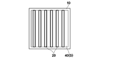
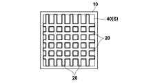
図1Aに示されるパターン以外には、図2Aに示されるストライプ状のパターンや、図2Bに示される格子状のパターン等を用いることができる。ストライプ状のパターンは、より細かい補正が実施でき、格子状のパターンは、副走査方向のジッタ補正にも有効である。チェッカーボード形状等の微細なパターンは、局所的な場所を精密に特定する測定に有効である。
マーカーパターン20は、感度良く信号光を検出可能とするためには、50nm以上の厚みを有していることが好ましい。
透明微細凹凸構造30としては、その上に成膜される金膜の表面である微細凹凸構造40の表面において局在プラズモンが誘起されうる凹凸構造(平均深さ、平均ピッチ)であれば特に制限されない。透明微細凹凸構造30としては、バイヤーライト層又はベーマイト層が好ましく、形成方法が容易であり、凹凸構造の面内均一性が高いことからベーマイト層であることが最も好ましい。ベーマイトを用いた光電場増強デバイス1を用いた態様では、表面凹凸構造の面内均一性が高いので、同一試料に対して、光照射箇所を変えて測定を実施しても、再現性のよいデータが得られる。したがって、同一試料に対して、光照射箇所を変えて複数のデータを取り、データの信頼性を上げることが可能である。
上記透明微細凹凸構造30としては、その他にアルミニウムを陽極酸化した後に非陽極酸化部分を除去して得られる陽極酸化アルミニウム皮膜等が例示される。また、本実施形態では透明基板10と透明微細凹凸構造30とが異なる材料により構成された態様について示してあるが、透明基板10の表面を加工して透明微細凹凸構造30を形成した態様であってもよく、この場合は、透明基板10と透明微細凹凸構造30とが一体化されてなる構成となる。かかる構成は、例えば、ガラス基板の表面をリソグラフィーとドライエッチング処理することにより形成することができる。
金属膜からなる微細凹凸構造40としては特に制限されず、励起光L1の照射により良好な局在プラズモンを誘起可能な金属であることが好ましい。かかる金属としては、Au、Ag、Cu、Al、Pt、およびこれらを主成分とする合金等が挙げられ、Auが特に好ましい。
金属膜からなる微細凹凸構造40は、その凹凸の凸部の平均的な大きさおよび平均ピッチは、励起光L1の照射により表面において局在プラズモンを生じさせうるものであれば特に限定されないが、励起光L1の波長より短いことが好ましい。金属膜からなる微細凹凸構造40は、凸部頂点から隣接する凹部の底部までの平均深さが200nm以下、凹部を隔てた最隣接凸部の頂点同士の平均ピッチが200nm以下であることが望ましい。
金属膜からなる微細凹凸構造40は、本実施形態のように下地基材に微細凹凸構造30を備え、下地の凹凸構造に応じた微細凹凸構造を有するものであってもよいし、下地基材に表面平滑性の高い基材を用い、下地基材の表面の形状によらない微細凹凸構造を有するものであってもよい。ただし、下地の凹凸構造に応じた微細凹凸構造である場合でも、金属は凝集等をしやすいことから、下地と同じ形状のものとなるとは限らない。
マーカーパターン20と試料との焦点を考慮すると、マーカーパターン20は金属膜からなる微細凹凸構造40上に形成されてなることが好ましいと通常は考えられるが、ナノオーダーの極薄い微細凹凸構造上へのマーカーのパターニングは、微細凹凸構造に亀裂を生じやすく製造上困難である。本実施形態の構成によれば、微細凹凸構造に影響を与えることなく精度良い形状のマーカーパターンを形成することができる。
光電場増強デバイス1において、マーカーパターン20、透明微細凹凸構造30、金属膜からなる微細凹凸構造40の各層の厚みは、信号光L2の検出を裏面10s側からマーカーパターン20及び、試料Sからの信号光(反射光や吸収光)を感度良く検出可能な厚みとなるように設計されることが好ましい。なお、透明基板10については、その厚みが厚く、オーダーが全く異なるため考慮する必要はない(基板はミリオーダー、他の層はナノオーダー)。
裏面10s側からマーカーパターン20及び、試料Sからの信号光を感度良く検出可能とするためには、マーカーパターン20が基板10上に直接形成されてなることから、基板10の表面(マーカー形成面)と、金属膜からなる微細凹凸構造40の表面40sとが、信号光を検出する光学系の焦点深度内に存在する必要がある。
従って、透明微細凹凸構造30と金属膜からなる微細凹凸構造40との合計膜厚は、検出に用いられる光学系の焦点深度を考慮して設計する必要がある。
例えば、ラマン分光装置に適用する場合に、励起光として780nmのレーザを用い、透明基板10側から、倍率100倍、開口数0.9の顕微鏡レンズにて検出する系における焦点深度は約700nmである。この場合、透明微細凹凸構造30と金属膜からなる微細凹凸構造40との合計膜厚は700nm以下において、充分な電場増強効果が得られる膜厚であればよいことになる。
金属膜からなる微細凹凸構造40の平均膜厚は、励起光L1の照射により良好に局在プラズモンが誘起可能であり、10~100nmの範囲内であることが好ましい。
上記した焦点深度と局在プラズモンを良好に誘起可能である金属膜の膜厚を考慮した値であれば、透明微細凹凸構造30の厚みは特に制限されず、製造しやすい膜厚とすることが好ましい。例えば、透明微細凹凸構造30を200nmの膜厚で形成し、その上に金膜を50nmとすれば、合計膜厚が250nmであり、マーカーが形成される基板面と金属微細構造で形成される測定面は充分に焦点深度内の膜厚とすることができ、マーカーからの反射光と信号光を同時に感度良く検出することができる。
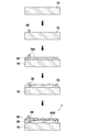
次に、図3を参照して、光電場増強デバイス1の製造方法について、透明微細凹凸構造30としてベーマイト層を備えた態様を例に説明する。
まず板状の透明基板10を用意し、透明基板10を純水洗浄したのち、マーカーパターン20をパターン形成する。
まず板状の透明基板10を用意し、透明基板10を純水洗浄したのち、マーカーパターン20をパターン形成する。
パターン形成方法としては特に制限されないが、高精度なパターニングが可能なことから、光リソグラフィ技術により形成されることが好ましい。
その後、表面を純水洗浄した後、透明基板10及びマーカーパターン20の表面にスパッタ法によりアルミニウム層30aを数十nm程度の膜厚にて成膜する。
次いで、純水を沸騰させた中に、アルミニウム層30a付き透明基板10を浸水させ、数分(5分程度)後に取り出す。この煮沸処理(ベーマイト処理)により、アルミニウム層は透明化し、透明微細凹凸構造(ベーマイト層)30が形成される。
得られたベーマイト層30上に、Au等の金属膜を蒸着により成膜し、少なくとも表面に金属微細凹凸構造40を備えた光電場増強デバイス1を得ることができる。なお、金属膜40は、蒸着に限らず、たとえば金属の微粒子を固定化して形成するようにしてもよい。また、蒸着法についても、通常の蒸着法に限らず、斜め蒸着法を用いてもよい。
以上のようにして光電場増強デバイスは製造することができる。
以上のようにして光電場増強デバイスは製造することができる。
次に、光電場増強デバイス1を用いてイメージングを実施する測定装置100について説明する。図4は、測定装置100の構成を示す概略断面図である。
図4に示すように、測定装置100は、試料Sを表面40Sに載置した光電場増強デバイス1と、光電場増強デバイス1の裏面10s側(透明基板10側)から試料Sへ励起光L1を照射する励起光照射手段110と、励起光L1をデバイス1の表面内方向に2次元走査させる走査手段140と、試料S中の被検体から発せられ光電場増強デバイス1の作用により増強された各走査点からの信号光L2を、裏面10s側から検出する検出手段120と、検出手段120により検出された走査点からの信号光L2に基づいて、表面40sにおける2次元信号画像及びマーカーパターン画像を取得する画像取得手段130と、マーカーパターン20の画像に基づいて、取得された2次元信号画像を補正する画像補正手段150と、画像補正手段150により補正された2次元信号画像を表示する表示手段160とを備えている。
本発明の測定装置において、既に述べたように、光電場増強デバイス1は、透明基板10のマーカーパターン形成面と、微細凹凸構造表面40sとの距離は、検出手段の焦点深度以内となるように設計されている。
励起光照射手段110は、励起光L1を射出する励起光源111と、励起光L1を基板10側へ透過させ、該励起光L1の照射により試料S中の被検体から生じ増強された信号光L2を含む基板10側からの光を光検出部120側へ反射させるダイクロイックミラー112と、該ダイクロイックミラー112を透過した励起光L1を光電場増強デバイス1の試料S載置された領域に集光すると共に、試料側からの光を平行光化するレンズ113とを備えている。
励起光照射手段110には、必要に応じて、励起光源111から射出された光L1を特定の波長の励起光とするレーザーラインフィルタ等を備えてもよい。
光検出手段120は、透明基板10の裏面側に配置されてなり、信号光L2を含みダイクロイックミラー112を透過してきた光のうち励起光L1を吸収し、それ以外の光を透過するノッチフィルタ122と、分光器等の光検出器121とを備えている。光検出手段121には、ノッチフィルタ122と光検出器121との間に、ノイズ光を除去して分光器等の光検出器121に信号光L2を平行光化して入射させるスリット及びレンズ対を備えていることが好ましい。ラマン散乱光を検出する場合、分光器を備えた態様では、入射されたラマン散乱光Lsが分光されてラマンスペクトルが得られる。
光検出器120により検出は、走査手段140により図1に示された主走査方向及び副走査方向に走査するとともに所定の間隔で配された各走査点において実施され、各走査点において検出された信号光L2の強度やスペクトル等の検出結果は、画像取得手段130に送られる。
画像取得手段130では、各走査点の検出結果に基づいて、表面40sにおける2次元信号画像及びマーカーパターン画像を取得する。例えば、得られる検出結果がラマンスペクトルのような分光結果である場合には、得られるスペクトルパターンの中から所望の波長を決定し、表面40sにおける各走査点に対応する位置に、得られた信号を表示することによって、ラマンスペクトルの検出結果を可視化して2次元のイメージングを行うことができる。
しかしながら、この段階で得られる2次元画像はジッタのずれを含んだ画像である。測定装置100では、試料における2次元画像と共に、マーカーパターン20の2次元画像も得られている。測定装置100の画像取得手段130において得られる画像の模式図を図5の左側に示す。
図示されるように、ジッタのずれを含んだ画像は、マーカー信号画像と同様のずれを含んでいることになる。従って、予め、正しいマーカー信号画像を画像補正手段150に記憶しておき、画像補正手段150にて、画像取得手段130において得られた2次元信号画像を、記憶されている正しいマーカー信号画像に基づいて、測定されたマーカー信号画像を正しく補正するように補正することにより、ジッタのずれを除去した正しい2次元信号画像を取得することができる。
画像補正手段150により補正された2次元信号画像は、それを表示する表示手段160に送られて、図5右図のような正しい2次元信号画像として表示される。
光電場増強デバイス1及びそれを用いた測定装置100は、ラマン散乱光、蛍光、高次高調波、レーリー散乱光あるいはミー散乱光等のケミカルイメージングに好適に使用することができる。
光電場増強デバイス1は、透明基板10と、透明基板10上に直接形成され、2次元走査における主走査方向と非平行方向に延びるマーカーパターン20と、マーカーパターン20及び透明基板10上に形成された少なくとも表面40sが金属膜40からなる微細凹凸構造(30,40)を備えた構成としている。かかる構成の光電場増強デバイスを用いたケミカルイメージング測定では、励起光L1照射のジッタに基づく2次元画像のずれを、マーカーパターン20の画像のずれ量に基づいて補正することにより補正して精度の高い信号画像を取得することができる。また、光電場増強デバイス1は、励起光L1や信号光L2に対して透明な材料により構成していることから、試料の信号光L2の検出やマーカーパターン20の検出を光電場増強デバイスの裏面10s側(試料接触面と反対側)から実施することができる。従って、本発明によれば、精密な機械制御を要することなく精度の高い信号画像を取得可能であり、細胞などのμmオーダー以上の試料であっても高いS/Nにてケミカルイメージングを実施することができる。
「設計変更」
上記実施形態において、励起光照射手段110は光検出手段120と共に、光電場増強デバイス1の裏面側に配置され、裏面側から励起光を照射する構成について説明したが、励起光照射手段110は、光電場増強デバイス1の表面側(被検体配置面側)に配置し、表面側から励起光を照射する構成としてもよい。光電場増強デバイスの金属微細凹凸構造に対しては、表裏のいずれから励起光が入射されても同様に局在プラズモン共鳴を誘起することができ、光電場増強効果を得ることができる。
上記実施形態において、励起光照射手段110は光検出手段120と共に、光電場増強デバイス1の裏面側に配置され、裏面側から励起光を照射する構成について説明したが、励起光照射手段110は、光電場増強デバイス1の表面側(被検体配置面側)に配置し、表面側から励起光を照射する構成としてもよい。光電場増強デバイスの金属微細凹凸構造に対しては、表裏のいずれから励起光が入射されても同様に局在プラズモン共鳴を誘起することができ、光電場増強効果を得ることができる。
Claims (12)
- 励起光の照射により表面に局在プラズモンが誘起され、前記照射により前記表面に載置された試料から発せられる信号光の強度を増強する光電場増強デバイスであって、
前記表面に対して、前記励起光を前記表面内方向に2次元走査して、各走査点からの各前記信号光を裏面側から検出し、該検出により得られた各信号光に基づいて前記表面における2次元信号画像を取得する測定方法に用いられるものであり、
透明基板と、
該透明基板上に直接形成され、前記2次元走査における主走査方向と非平行方向に延びるマーカーパターンと、
該マーカーパターン及び前記透明基板上に形成された少なくとも表面が金属膜からなる微細凹凸構造を備えたことを特徴とする光電場増強デバイス。 - 前記微細凹凸構造が、バイヤーライト又はベーマイトからなる透明微細凹凸構造の凹凸面に金属膜が成膜されてなるものであることを特徴とする請求項1に記載の光電場増強デバイス。
- 前記マーカーパターンが、前記主走査方向と略垂直に交わるライン状のパターンであることを特徴とする請求項1又は2に記載の光電場増強デバイス。
- 前記マーカーパターンが、前記励起光に対する反射率が高い材料により形成されてなることを特徴とする請求項1~3のいずれかに記載の光電場増強デバイス。
- 前記マーカーパターンが、Cr,Au,Al,又はAgのうち少なくとも1種の金属により形成されてなることを特徴とする請求項4に記載の光電場増強デバイス。
- 前記マーカーパターンが、前記励起光に対する吸収率が高い材料により形成されてなることを特徴とする請求項1~3のいずれかに記載の光電場増強デバイス。
- 前記マーカーパターンが、カーボンブラック又は窒化チタンのうち少なくとも1種より形成されてなることを特徴とする請求項6に記載の光電場増強デバイス。
- 前記マーカーパターンが、前記励起光の照射により蛍光を発する材料により形成されてなることを特徴とする請求項1~3のいずれかに記載の光電場増強デバイス。
- 請求項1~8のいずれかに記載の光電場増強デバイスと、
前記励起光を前記表面に照射する励起光照射手段と、
前記励起光を前記表面内方向に2次元走査させる走査手段と、
前記各走査点からの前記各信号光を前記裏面側から検出する検出手段と、
該検出手段により検出された前記走査点からの信号光に基づいて、前記表面における前記2次元信号画像及び前記マーカーパターン画像を取得する画像取得手段と、
該マーカーパターン画像に基づいて、前記取得された2次元信号画像を補正する画像補正手段と、
該画像補正手段により補正された前記2次元信号画像を表示する表示手段を備えたことを特徴とする測定装置。 - 前記透明基板の前記マーカーパターン形成面と、前記表面との距離が、前記検出手段の焦点深度以内であることを特徴とする請求項9に記載の測定装置。
- 励起光の照射により表面に局在プラズモンが誘起され、前記照射により前記表面に載置された試料から発せられる信号光の強度を増強するものであり、
前記表面に対して、前記励起光を前記表面内方向に2次元走査して、各走査点からの各前記信号光を裏面側から検出し、該検出により得られた各信号光に基づいて前記表面における2次元信号画像を取得する測定方法に用いられる光電場増強デバイスの製造方法であって、
透明基板を用意し、
該透明基板上に、前記2次元走査における主走査方向と非平行方向に延びるマーカーパターンを直接形成し、
該マーカーパターンが形成された前記透明基板上に、
アルミニウムを主成分とする金属膜を形成し、
少なくとも該金属膜を浸水させた後に煮沸処理を施すことによりベーマイト層を形成し、
該ベーマイト層上に金属膜を形成することを特徴とする光電場増強デバイスの製造方法。 - 前記マーカーパターンを、リソグラフィにより形成することを特徴とする請求項11に記載の光電場増強デバイスの製造方法。
Priority Applications (1)
| Application Number | Priority Date | Filing Date | Title |
|---|---|---|---|
| US14/668,584 US9645087B2 (en) | 2012-09-28 | 2015-03-25 | Measuring apparatus where a distance between a surface of a transparent substrate on which a marker pattern is formed and a front surface is within a depth of focus of a detecting means |
Applications Claiming Priority (2)
| Application Number | Priority Date | Filing Date | Title |
|---|---|---|---|
| JP2012-217669 | 2012-09-28 | ||
| JP2012217669A JP5947182B2 (ja) | 2012-09-28 | 2012-09-28 | 光電場増強デバイスを用いた測定装置 |
Related Child Applications (1)
| Application Number | Title | Priority Date | Filing Date |
|---|---|---|---|
| US14/668,584 Continuation US9645087B2 (en) | 2012-09-28 | 2015-03-25 | Measuring apparatus where a distance between a surface of a transparent substrate on which a marker pattern is formed and a front surface is within a depth of focus of a detecting means |
Publications (1)
| Publication Number | Publication Date |
|---|---|
| WO2014050133A1 true WO2014050133A1 (ja) | 2014-04-03 |
Family
ID=50387565
Family Applications (1)
| Application Number | Title | Priority Date | Filing Date |
|---|---|---|---|
| PCT/JP2013/005755 Ceased WO2014050133A1 (ja) | 2012-09-28 | 2013-09-27 | 光電場増強デバイスとその製造方法、及びそれを用いた測定装置 |
Country Status (3)
| Country | Link |
|---|---|
| US (1) | US9645087B2 (ja) |
| JP (1) | JP5947182B2 (ja) |
| WO (1) | WO2014050133A1 (ja) |
Cited By (1)
| Publication number | Priority date | Publication date | Assignee | Title |
|---|---|---|---|---|
| WO2014167828A1 (ja) * | 2013-04-08 | 2014-10-16 | 富士フイルム株式会社 | 測定用デバイス、測定装置および方法 |
Families Citing this family (1)
| Publication number | Priority date | Publication date | Assignee | Title |
|---|---|---|---|---|
| KR102677257B1 (ko) * | 2021-01-25 | 2024-06-25 | 주식회사 나노엔텍 | 다채널 시료 칩을 이용한 미세입자 계수방법 및 이를 구현한 미세입자 계수장치 |
Citations (4)
| Publication number | Priority date | Publication date | Assignee | Title |
|---|---|---|---|---|
| JP2002168786A (ja) * | 2000-12-04 | 2002-06-14 | Fuji Photo Film Co Ltd | スキャナにおけるジッターの防止方法およびジッターの発生を防止可能なスキャナ |
| JP2003248007A (ja) * | 2002-02-25 | 2003-09-05 | Matsushita Electric Ind Co Ltd | 分析装置 |
| JP2012063294A (ja) * | 2010-09-17 | 2012-03-29 | Fujifilm Corp | 光電場増強デバイスを用いた光の測定方法および測定装置 |
| US20120236301A1 (en) * | 2011-03-18 | 2012-09-20 | Seiko Epson Corporation | Measurement apparatus and measurement method |
Family Cites Families (8)
| Publication number | Priority date | Publication date | Assignee | Title |
|---|---|---|---|---|
| JP2000055809A (ja) | 1998-08-13 | 2000-02-25 | Nikon Corp | 顕微ラマン分光装置及び顕微ラマン分光測定方法 |
| US6970239B2 (en) | 2002-06-12 | 2005-11-29 | Intel Corporation | Metal coated nanocrystalline silicon as an active surface enhanced Raman spectroscopy (SERS) substrate |
| US7361313B2 (en) | 2003-02-18 | 2008-04-22 | Intel Corporation | Methods for uniform metal impregnation into a nanoporous material |
| JP4163606B2 (ja) | 2003-12-10 | 2008-10-08 | 富士フイルム株式会社 | 微細構造体、微細構造体の作製方法、ラマン分光方法および装置 |
| JP2006145230A (ja) | 2004-11-16 | 2006-06-08 | Canon Inc | 被分析物担体およびその製造方法 |
| JP2007147357A (ja) | 2005-11-25 | 2007-06-14 | Nano Photon Kk | ラマン顕微鏡及びラマンスペクトルイメージの表示方法 |
| JP5080186B2 (ja) * | 2007-09-26 | 2012-11-21 | 富士フイルム株式会社 | 分子分析光検出方法およびそれに用いられる分子分析光検出装置、並びにサンプルプレート |
| JP5552007B2 (ja) | 2010-09-17 | 2014-07-16 | 富士フイルム株式会社 | 光電場増強デバイス |
-
2012
- 2012-09-28 JP JP2012217669A patent/JP5947182B2/ja not_active Expired - Fee Related
-
2013
- 2013-09-27 WO PCT/JP2013/005755 patent/WO2014050133A1/ja not_active Ceased
-
2015
- 2015-03-25 US US14/668,584 patent/US9645087B2/en not_active Expired - Fee Related
Patent Citations (4)
| Publication number | Priority date | Publication date | Assignee | Title |
|---|---|---|---|---|
| JP2002168786A (ja) * | 2000-12-04 | 2002-06-14 | Fuji Photo Film Co Ltd | スキャナにおけるジッターの防止方法およびジッターの発生を防止可能なスキャナ |
| JP2003248007A (ja) * | 2002-02-25 | 2003-09-05 | Matsushita Electric Ind Co Ltd | 分析装置 |
| JP2012063294A (ja) * | 2010-09-17 | 2012-03-29 | Fujifilm Corp | 光電場増強デバイスを用いた光の測定方法および測定装置 |
| US20120236301A1 (en) * | 2011-03-18 | 2012-09-20 | Seiko Epson Corporation | Measurement apparatus and measurement method |
Cited By (3)
| Publication number | Priority date | Publication date | Assignee | Title |
|---|---|---|---|---|
| WO2014167828A1 (ja) * | 2013-04-08 | 2014-10-16 | 富士フイルム株式会社 | 測定用デバイス、測定装置および方法 |
| JP2014202650A (ja) * | 2013-04-08 | 2014-10-27 | 富士フイルム株式会社 | 測定用デバイス、測定装置および方法 |
| US9728388B2 (en) | 2013-04-08 | 2017-08-08 | Fujifilm Corporation | Measurement device, measurement apparatus, and method |
Also Published As
| Publication number | Publication date |
|---|---|
| JP5947182B2 (ja) | 2016-07-06 |
| US20150198536A1 (en) | 2015-07-16 |
| JP2014071014A (ja) | 2014-04-21 |
| US9645087B2 (en) | 2017-05-09 |
Similar Documents
| Publication | Publication Date | Title |
|---|---|---|
| CN103109179B (zh) | 光电场增强设备 | |
| JP5553717B2 (ja) | 光電場増強デバイスを用いた光の測定方法および測定装置 | |
| JP5848013B2 (ja) | 光電場増強デバイスおよび該デバイスを備えた測定装置 | |
| JP5957825B2 (ja) | ラマン分光装置およびラマン分光測定法 | |
| US20140242573A1 (en) | Optical element, analysis device, analysis method and electronic apparatus | |
| WO2006135097A1 (en) | Sensor, multichannel sensor, sensing apparatus, and sensing method | |
| US10627217B2 (en) | Method for determining the thickness of a contaminating layer and/or the type of contaminating material, optical element and EUV-lithography system | |
| WO2013080505A1 (ja) | センシング装置およびこれを用いたセンシング方法 | |
| JP5947182B2 (ja) | 光電場増強デバイスを用いた測定装置 | |
| WO2015146036A1 (ja) | 増強ラマン分光装置 | |
| JP5947181B2 (ja) | 光電場増強デバイスを用いた光測定装置 | |
| JP2013176436A (ja) | 生体成分濃度測定装置 | |
| JP2014016221A (ja) | 光電場増強デバイスおよびその製造方法 | |
| WO2012160774A1 (ja) | ラマン分光測定装置、並びにラマン分光測定装置用光ファイバおよびその作製方法 | |
| CN103698279B (zh) | 一种测量单个纳米粒子光谱的方法 | |
| JP2006329699A (ja) | 微小開口カンチレバーおよびそれを用いた近接場分光装置 | |
| JP6145881B2 (ja) | ラマン分光画像取得システムおよびラマン分光画像取得方法 | |
| JP2015232526A (ja) | ラマン分光分析用信号増幅装置、ラマン分光分析装置及びラマン分光分析方法 | |
| JP2016003858A (ja) | 検出装置、検出方法、および電場増強素子 |
Legal Events
| Date | Code | Title | Description |
|---|---|---|---|
| 121 | Ep: the epo has been informed by wipo that ep was designated in this application |
Ref document number: 13841359 Country of ref document: EP Kind code of ref document: A1 |
|
| NENP | Non-entry into the national phase |
Ref country code: DE |
|
| 122 | Ep: pct application non-entry in european phase |
Ref document number: 13841359 Country of ref document: EP Kind code of ref document: A1 |