WO2014044813A2 - Optoelektronisches bauelement umfassend ein transparentes auskoppelelement - Google Patents
Optoelektronisches bauelement umfassend ein transparentes auskoppelelement Download PDFInfo
- Publication number
- WO2014044813A2 WO2014044813A2 PCT/EP2013/069608 EP2013069608W WO2014044813A2 WO 2014044813 A2 WO2014044813 A2 WO 2014044813A2 EP 2013069608 W EP2013069608 W EP 2013069608W WO 2014044813 A2 WO2014044813 A2 WO 2014044813A2
- Authority
- WO
- WIPO (PCT)
- Prior art keywords
- group
- same
- fully
- partially substituted
- hybrid material
- Prior art date
- Legal status (The legal status is an assumption and is not a legal conclusion. Google has not performed a legal analysis and makes no representation as to the accuracy of the status listed.)
- Ceased
Links
Classifications
-
- H—ELECTRICITY
- H10—SEMICONDUCTOR DEVICES; ELECTRIC SOLID-STATE DEVICES NOT OTHERWISE PROVIDED FOR
- H10H—INORGANIC LIGHT-EMITTING SEMICONDUCTOR DEVICES HAVING POTENTIAL BARRIERS
- H10H20/00—Individual inorganic light-emitting semiconductor devices having potential barriers, e.g. light-emitting diodes [LED]
- H10H20/80—Constructional details
- H10H20/85—Packages
- H10H20/852—Encapsulations
- H10H20/854—Encapsulations characterised by their material, e.g. epoxy or silicone resins
-
- H—ELECTRICITY
- H10—SEMICONDUCTOR DEVICES; ELECTRIC SOLID-STATE DEVICES NOT OTHERWISE PROVIDED FOR
- H10H—INORGANIC LIGHT-EMITTING SEMICONDUCTOR DEVICES HAVING POTENTIAL BARRIERS
- H10H20/00—Individual inorganic light-emitting semiconductor devices having potential barriers, e.g. light-emitting diodes [LED]
- H10H20/80—Constructional details
- H10H20/85—Packages
- H10H20/8506—Containers
-
- H—ELECTRICITY
- H10—SEMICONDUCTOR DEVICES; ELECTRIC SOLID-STATE DEVICES NOT OTHERWISE PROVIDED FOR
- H10H—INORGANIC LIGHT-EMITTING SEMICONDUCTOR DEVICES HAVING POTENTIAL BARRIERS
- H10H20/00—Individual inorganic light-emitting semiconductor devices having potential barriers, e.g. light-emitting diodes [LED]
- H10H20/80—Constructional details
- H10H20/85—Packages
- H10H20/851—Wavelength conversion means
- H10H20/8511—Wavelength conversion means characterised by their material, e.g. binder
-
- H—ELECTRICITY
- H10—SEMICONDUCTOR DEVICES; ELECTRIC SOLID-STATE DEVICES NOT OTHERWISE PROVIDED FOR
- H10H—INORGANIC LIGHT-EMITTING SEMICONDUCTOR DEVICES HAVING POTENTIAL BARRIERS
- H10H20/00—Individual inorganic light-emitting semiconductor devices having potential barriers, e.g. light-emitting diodes [LED]
- H10H20/80—Constructional details
- H10H20/85—Packages
- H10H20/851—Wavelength conversion means
- H10H20/8515—Wavelength conversion means not being in contact with the bodies
-
- H—ELECTRICITY
- H10—SEMICONDUCTOR DEVICES; ELECTRIC SOLID-STATE DEVICES NOT OTHERWISE PROVIDED FOR
- H10H—INORGANIC LIGHT-EMITTING SEMICONDUCTOR DEVICES HAVING POTENTIAL BARRIERS
- H10H20/00—Individual inorganic light-emitting semiconductor devices having potential barriers, e.g. light-emitting diodes [LED]
- H10H20/80—Constructional details
- H10H20/85—Packages
- H10H20/852—Encapsulations
- H10H20/853—Encapsulations characterised by their shape
-
- H—ELECTRICITY
- H10—SEMICONDUCTOR DEVICES; ELECTRIC SOLID-STATE DEVICES NOT OTHERWISE PROVIDED FOR
- H10H—INORGANIC LIGHT-EMITTING SEMICONDUCTOR DEVICES HAVING POTENTIAL BARRIERS
- H10H20/00—Individual inorganic light-emitting semiconductor devices having potential barriers, e.g. light-emitting diodes [LED]
- H10H20/80—Constructional details
- H10H20/85—Packages
- H10H20/855—Optical field-shaping means, e.g. lenses
-
- H—ELECTRICITY
- H10—SEMICONDUCTOR DEVICES; ELECTRIC SOLID-STATE DEVICES NOT OTHERWISE PROVIDED FOR
- H10W—GENERIC PACKAGES, INTERCONNECTIONS, CONNECTORS OR OTHER CONSTRUCTIONAL DETAILS OF DEVICES COVERED BY CLASS H10
- H10W74/00—Encapsulations, e.g. protective coatings
- H10W74/40—Encapsulations, e.g. protective coatings characterised by their materials
- H10W74/47—Encapsulations, e.g. protective coatings characterised by their materials comprising organic materials, e.g. plastics or resins
-
- H—ELECTRICITY
- H10—SEMICONDUCTOR DEVICES; ELECTRIC SOLID-STATE DEVICES NOT OTHERWISE PROVIDED FOR
- H10H—INORGANIC LIGHT-EMITTING SEMICONDUCTOR DEVICES HAVING POTENTIAL BARRIERS
- H10H20/00—Individual inorganic light-emitting semiconductor devices having potential barriers, e.g. light-emitting diodes [LED]
- H10H20/80—Constructional details
- H10H20/85—Packages
- H10H20/851—Wavelength conversion means
- H10H20/8514—Wavelength conversion means characterised by their shape, e.g. plate or foil
Definitions
- Optoelectronic component comprising a transparent Auskoppelelernent
- LEDs Light-emitting diodes
- transparent coupling-out elements such as, for example, an encapsulation made of polymeric materials. These polymeric materials often exhibit exposure to light and heat
- Object of at least one embodiment of the present invention is therefore to provide an optoelectronic device with a transparent coupling element, which is characterized by an increased stability to light and heat.
- the optoelectronic component comprises a layer sequence with an active layer which emits electromagnetic primary radiation and at least one transparent outcoupling element which is arranged in the beam path of the electromagnetic primary radiation.
- the at least one transparent outcoupling element which is arranged in the beam path of the electromagnetic primary radiation.
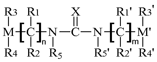
- Decoupling element comprises a hybrid material or is made of a hybrid material, which has the following structure:
- R 1, R 1, R 2, R 2 'and R 5 may be the same or different and are selected from the group consisting of H, saturated and unsaturated alkyl radicals, fully or partially substituted, saturated and unsaturated
- Alkyl radicals aromatics, in whole or in part
- R3, R3 ', R4 and R4' may be the same or different and are selected from the group consisting of H, saturated and unsaturated alkyl radicals, fully or partially substituted, saturated and unsaturated
- X is selected from a group comprising 0, S and N-R6 wherein R6 is selected from the same group as R1, R1 'R2, R2' and R5.
- M and M ' may be the same or different and are selected from a group comprising B, Al, Si-R7, Ge-R7' and Ti-R7 ''.
- R7, R7 'and R7' ' may be chosen the same or different and are selected from the same group as R3, R3', R4 and R4 '.
- Y is selected from a group comprising 0, S, N-R5 'and a bond wherein R5' is selected from the same group as R1, R1 'R2, R2' and R5 and R5 'are the same or
- R1, R1 'R2, R2' and R5 can be selected.
- Y can be a bond means that a compound of the following formula is present:
- n, m can be chosen to be the same or different, where and 1 ⁇ n, m ⁇ 10000. Preference is given to 1 ⁇ n, m ⁇ 5000,
- R 1, R 1', R 2 ', R 2', R 5 and R 5 ' may be the same or different and may be selected from a group comprising H, saturated and unsaturated alkyl radicals, fully or partially substituted, saturated and unsaturated alkyl radicals, aromatics, fully or partially substituted aromatics, heterocycles and fully or partially substituted heterocycles.
- R6 can be selected from the same group as R1, R1' R2, R2 ', R5 and R5'.
- Decoupling elements which comprise a hybrid material or are made of a hybrid material, have a high
- this high stability is due to the high binding stability of the structural unit
- the abrasion resistance is the
- Optoelectronic device can be prevented and extended the life of the optoelectronic device.
- this includes at least one
- R 1, R 1, R 2, R 2 'and R 5 may be the same or different and are selected from the group consisting of H, saturated, fully or partially substituted, saturated alkyl radicals, aromatics, fully or partially substituted aromatics, heterocycles and fully or partially substituted Heterocycles includes.
- R3, R3 ', R4 and R4' may be the same or different and are selected from the group consisting of H, saturated alkyl, wholly or partially
- the at least one transparent decoupling element comprises a hybrid material or is made of a hybrid material, which has the following structure:
- Decoupling elements comprising such a hybrid material or made of such a hybrid material, have a very high stability to heat and
- the hybrid materials can be achieved by simple
- Decoupling elements comprising a hybrid material or made of a hybrid material are very simple and inexpensive to produce.
- electromagnetic spectrum for electromagnetic radiation in the UV range and in the infrared range or a partial spectrum thereof is almost completely permeable.
- Layer sequence emitted primary radiation for example, in the visible range or in the UV range of
- the decoupling element has a transparency of more than 95%, particularly preferably the transparency of the decoupling element is more than 98% for the emitted primary radiation.
- layer sequence is to be understood as meaning a layer sequence comprising more than one layer, for example a sequence comprising at least one p-doped and an n-doped semiconductor layer, wherein the
- Layers are arranged one above the other.
- the layer sequence can be used as an epitaxial layer sequence or as a radiation-emitting semiconductor chip with a
- the layer sequence can be implemented, for example, on the basis of InGaAlN. InGaAlN-based semiconductor chips and
- Semiconductor layer sequences are in particular those in which the epitaxially produced semiconductor layer sequence has a layer sequence of different individual layers
- Semiconductor layer sequences comprising at least one active layer based on InGaAlN, for example, electromagnetic radiation in a
- the semiconductor layer sequence or the semiconductor chip may also be based on InGaAlP, that is, the semiconductor layer sequence may be different
- Single layers may have, of which at least one
- semiconductor layer sequences or semiconductor chips having at least one active layer based on InGaAlP may emit electromagnetic radiation having one or more spectral components in a green to red wavelength range.
- the semiconductor layer sequence or the semiconductor chip can also comprise other III-V compound semiconductor material systems, for example an AlGaAs-based material, or II-VI compound semiconductor material systems.
- an active layer based on InGaAlP may emit electromagnetic radiation having one or more spectral components in a green to red wavelength range.
- the semiconductor layer sequence or the semiconductor chip can also comprise other III-V compound semiconductor material systems, for example an AlGaAs-based material, or II-VI compound semiconductor material systems.
- an active layer based on InGaAlP may emit electromagnetic radiation having one or more spectral components in a green to red wavelength range.
- the semiconductor layer sequence or the semiconductor chip can also comprise other III-V compound semiconductor material systems, for example an AlGaAs-based material, or II-VI compound semiconductor material systems.
- a layer comprising an AlGaAs-based material may be capable of emitting electromagnetic radiation with one or more spectral components in a red to an infrared
- Wavelength range to emit
- the active semiconductor layer sequence can contain, in addition to the active layer, further functional layers and functional layers
- Areas include, such as p- or n-doped
- Charge carrier transport layers ie electron or
- Barrier layers planarization layers, buffer layers, protective layers and / or electrodes and combinations thereof. Furthermore, for example, on a the
- Semiconductor layer sequence may be applied one or more mirror layers.
- the structures described here concerning the active layer or the further functional layers and regions are the person skilled in the art in particular
- the radicals R6 are from a
- R6 may be methyl, ethyl, propyl, isopropyl, butyl, isobutyl, sec-butyl, tert-butyl, Be cyclohexyl or phenyl. More preferably, R6 is H.
- R3, R3 ', R4, R4', R7, R7 'and R7' ' are preferably selected from the group consisting of H, saturated alkyl radicals, fully or partially substituted, saturated alkyl radicals,
- Alkyl radicals may be, for example, methyl, ethyl, propyl, isopropyl, butyl, isobutyl, sec-butyl, tert-butyl,
- R3, R3 ', R4, R4', R7, R7 'and R7' ' are selected from a group consisting of
- R3 and R3 'and / or R4, R4' are the same. Includes the decoupling element
- Hybrid material or is the decoupling of a
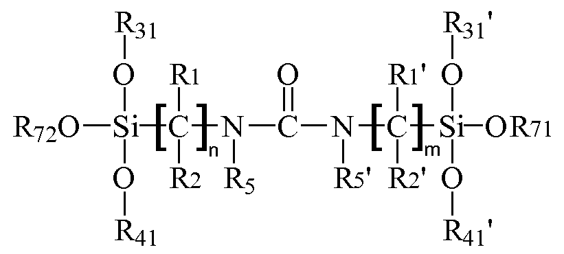
- the at least one transparent decoupling element comprises a hybrid material or is made of a hybrid material, which has the following structure:
- R41 R4l ' R31, R31 ', R41 and R41' can be chosen to be identical or different and are selected from a group which condensed H, saturated and unsaturated alkyl radicals, fully or partially substituted, saturated and unsaturated alkyl radicals, aromatics, fully or partially substituted aromatics Aromatics, fully or partially substituted, fused aromatics,
- R31, R31 ', R41 and R41' are preferably selected from the group consisting of H, saturated alkyl radicals, fully or partially substituted, saturated alkyl radicals, aromatics, fully or partially substituted aromatics,
- Heterocycles includes. More preferably, R31, R31 ', R41 and R41' are selected from the group consisting of H, saturated
- Alkyl radicals and fully or partially substituted, saturated alkyl radicals may be, for example, methyl, ethyl, propyl, isopropyl, butyl, isobutyl, sec-butyl, tert-butyl and cyclohexyl radicals.
- M ' is selected from a group comprising B, Al, Si-OR71, Ge-OR71' and Ti-OR71 ", wherein R71, R71 'and R71" may be the same or different and are selected from the same group as R31, R31 ', R41 and R41'.
- M is selected from a group comprising B, Al, Si-OR72, Ge-OR72 'and Ti-OR72''.
- R72, R72 'and R72 may be the same or different and are selected from the same group as R31, R31', R41 and R41 '. If the decoupling element comprises a hybrid material or if the decoupling element is made of a hybrid material which has the radicals R71 and R72, R71 'and R72' or R71 "and R72", R71 and R72, R71 'and R72' or R71 '' and R12 '' be chosen equal.
- R31 and R41 and / or R31 'and R41' are the same. Includes the decoupling element
- Hybrid material or is the decoupling of a
- R31 'and R41' correspond, so be selected identically. Does the coupling element comprises a hybrid material or is that
- Decoupling element prepared from a hybrid material having the radicals R72, R72 'or R72 ", R72, R72' or R72''denote R31 and R41 correspond, so be selected identically.
- X is one
- a decoupling element comprising such a hybrid material or made of such a hybrid material shows a very high stability to heat and radiation due to the high binding stability of the
- the high stability manifests itself in that the decoupling element in the presence of radiation in the visible, UV and
- Plastics and metals It also offers high elasticity and very good abrasion resistance.
- M and M 'are selected from a group comprising Si-R7 and Al. Most preferably, M and M 'are Si-R7.
- this comprises at least one
- Auskoppelelement a hybrid material or is made of a
- Hybrid material produced which has the following structure:
- R41 R41 ' wherein R31, R31', R41, R41 ', R71 and R72 are the same or
- H saturated alkyl radicals, fully or partially substituted, saturated alkyl radicals,
- Aromatics fully or partially substituted aromatics, heterocycles, fully or partially substituted
- Heterocycles includes.
- R 1, R 1 ', R 2, R 2' are selected from a group comprising H, saturated alkyl radicals, fully or partially substituted saturated alkyl radicals, aromatics, and fully or partially substituted aromatics.
- R 1, R 1 ', R 2, R 2' may be methyl, ethyl, propyl, isopropyl, butyl, isobutyl, sec-butyl, tert-butyl, cyclohexyl or phenyl radicals.
- R 1, R 1 ', R 2, R 2' are particularly preferably H.
- radicals R 1 and R 1 'and / or R 2 and R 2' can be chosen the same. It is also possible that the radicals and R 1 and R 2 and / or R 1 'and R 2' are chosen to be the same.
- R 5 and R 5 ' are selected from a group comprising H, saturated alkyl groups, and fully or partially substituted saturated alkyl groups.
- R5 and R5 ' may be methyl, ethyl, propyl, isopropyl, butyl, isobutyl, sec-butyl, tert-butyl,
- R5 and R5 ' may be the same or different. More preferably, R5 and R5 'are equal to H.
- the optoelectronic component may be a light emitting diode, a photodiode transistor array / module and an optical coupler.
- the optoelectronic component is an organic light-emitting diode (OLED).
- the optoelectronic component can be an LED with an electrical power of one watt and more.
- the at least one transparent decoupling element comprises converter particles.
- Converter particles are distributed in the decoupling element and at least partially convert the electromagnetic
- Primary radiation in an electromagnetic secondary radiation At least in part means that the electromagnetic primary radiation at least partially from the
- the electromagnetic primary radiation and / or secondary electromagnetic radiation may have one or more wavelengths and / or wavelength ranges in one
- Secondary radiation be narrowband, that is, the primary radiation and / or the secondary radiation then have a monochrome or approximately monochrome wavelength range.
- the spectrum of the primary radiation and / or the spectrum of the secondary radiation may alternatively also
- Wavelength range wherein the mixed-color wavelength range may have a continuous spectrum or a plurality of discrete spectral components with different wavelengths.
- the primary radiation and the secondary radiation can be
- the primary radiation can preferably give rise to a blue-colored luminous impression and the secondary radiation can produce a yellowish-colored luminous impression, which can result from spectral components of the secondary radiation in the yellow wavelength range and / or spectral components in the green and red wavelength ranges.
- Electromagnetic primary radiation is here completely or almost completely by the converter material is absorbed and in the form of an electromagnetic
- the emitted radiation of the optoelectronic component according to this embodiment thus corresponds completely or almost completely to the electromagnetic secondary radiation. Under almost
- Full conversion is a conversion over 90%, especially over 95% to understand.
- the primary radiation is in the UV range and the secondary radiation gives rise to a blue-colored and yellow-colored luminous impression, which can be caused by spectral components of the secondary radiation in the blue and yellow wavelength range and / or spectral components in the blue, green and red wavelength range.
- the secondary radiation gives rise to a blue-colored and yellow-colored luminous impression, which can be caused by spectral components of the secondary radiation in the blue and yellow wavelength range and / or spectral components in the blue, green and red wavelength range.
- the electromagnetic secondary radiation is in a blue to infrared
- the decoupling element has a transparency of over 95% for the emitted
- Secondary radiation particularly preferably is the
- the converter particles have a
- the converter particles preferably have a particle diameter of 5 to 15 ⁇ m, particularly preferably 10 ⁇ m.
- the converter particles may, for example, be formed from one of the following phosphors: rare earth doped garnets, rare earth doped alkaline earth sulfides, rare earth doped thiogallates, rare earth doped aluminates, rare earth doped metals Silicates, such as orthosilicates, rare earth doped chlorosilicates, rare earth doped alkaline earth silicon nitrides, rare earth doped oxynitrides and rare earth doped aluminum oxynitrides, rare earth doped silicon nitrides, sialons.
- garnets such as
- Yttrium aluminum oxide YAG
- LuAG lutetium aluminum oxide
- TAG terbium aluminum oxide
- the phosphors are, for example, doped with one of the following activators: cerium, europium, terbium, praseodymium, samarium, manganese.
- the converter particles are present at 1 to 50% by volume with respect to the hybrid material. Preference is given to 10 to 40% by volume, more preferably 20 to
- the converter particles are distributed homogeneously in the outcoupling element. Due to a homogeneous distribution of the converter particles is a uniform Conversion of the primary radiation by the converter particles possible, resulting in a uniform radiation characteristic of the secondary radiation result. According to one embodiment, this is at least one
- Decoupling element made of the hybrid material and the converter particles are by chemical bonds to the
- Hybrid material bound Under chemical bonds can covalent bonds, ionic bonds or coordinative bonds between the converter particles and the
- Hybrid material can be understood.
- this comprises at least one
- the nanoparticles are smaller than a tenth of the wavelength of the emitted primary radiation of the active layer of the layer sequence.
- the nanoparticles may have a size of 10 to 25 nm, 10 to 20 nm, more preferably 10 to 15 nm. On this scale, the nanoparticles scatter the primary radiation and / or
- the nanoparticles comprise
- the thermally conductive materials are selected from a group comprising Al 2 O 3 , AlN, SiO 2 and combinations thereof
- Optoelectronic device can be prevented and extended the life of the optoelectronic device.
- the nanoparticles comprise
- Decoupling elements having fillers with a refractive index n D at 23 ° C of greater than or equal to 2 show an increased light outcoupling, since light losses due to reflection and total reflection can be largely avoided.
- the light outcoupling is particularly high when the refractive index of the coupling-out element has a similar refractive index
- the fillers may be selected from a group comprising ZrÜ 2 , T1O 2 , b 2 Ü 5 , a 2 Ü 5, and combinations thereof.
- the filler is Zr0 2 -
- the nanoparticles can be bound to the hybrid material. Especially if M
- Si-R7 can be a very strong due to particularly strong ionic interactions of the silicon of the hybrid material with the nanoparticles, in particular with ZrÜ 2
- thermally conductive material and a filler containing a Refractive index n D at 23 ° C of greater than or equal to 2
- the nanoparticles are homogeneously distributed in the decoupling element, resulting in a uniform
- the optoelectronic device in one embodiment, the optoelectronic
- Component a housing.
- the housing may be present in particular in the middle of a recess.
- the layer sequence can be arranged in the recess. It is possible that the recess is filled with the layer sequence with a potting.
- the decoupling element is designed as a potting.
- the potting can fill the recess in the housing.
- the decoupling element is designed as a small plate, which is arranged above the layer sequence. It is possible that the tile is the whole
- the one layer or the one element is arranged indirectly on or above the other layer or the other element. It can then further layers and / or elements or a clear distance between the one or the other layer
- the first outcoupling element may be a potting compound comprising the hybrid material or made of the hybrid material.
- Decoupling element may be a plate, disposed over the layer sequence comprising the hybrid material or made of the hybrid material.
- the second outcoupling element is a lens made of the hybrid material or comprising the hybrid material. It is also possible that the first coupling element a
- Platelet disposed over the layer sequence made of the hybrid material or comprising the hybrid material.
- the first and second outcoupling elements may comprise the same hybrid materials or from the same
- the first and second include
- optoelectronic component at least one second
- decoupling elements in the form of a small plate are applied over the second and each further layer sequence.
- the platelet has a thickness of 10 ym to 100 ym, preferably 20 ym to 50 ym, more preferably 30 ym to 40 ym.
- the potting can be conventional
- an adhesion layer is arranged between the layer sequence and the platelet.
- an adhesive layer is disposed between the potting and the lens.
- the housing is made of a
- Hybrid material produced which has the following structure:
- R 1, R 1, R 2, R 2 'and R 5 may be the same or different and are selected from the group consisting of H, saturated and unsaturated alkyl radicals, fully or partially substituted, saturated and unsaturated
- Alkyl radicals aromatics, in whole or in part substituted aromatic, heterocyclic and fully or partially substituted heterocycles.
- R3, R3 ', R4 and R4' may be the same or different and are selected from the group consisting of H, saturated and unsaturated alkyl radicals, fully or partially substituted, saturated and unsaturated
- X is selected from a group comprising 0, S and N-R6 wherein R6 is selected from the same group as R1, R1 'R2, R2' and R5.
- M and M ' may be the same or different and are selected from a group comprising B, Al, Si-R7, Ge-R7' and Ti-R7 ''.
- R7, R7 'and R7' ' may be chosen the same or different and are selected from the same group as R3, R3', R4 and R4 '.
- Y is selected from a group comprising 0, S, N-R5 'and a bond wherein R5' is selected from the same group as R1, R1 'R2, R2' and R5 and is the same or
- Rl Rl 'R2, R2'
- Y can be a bond
- a compound of the following formula is present:
- n, m can be chosen to be the same or different, where and 1 ⁇ n, m ⁇ 10000. Preference is given to 1 ⁇ n, m ⁇ 5000,
- the housing is made of one
- Hybrid material produced which has the following structure:
- R 1, R 1, R 2, R 2 ', R 5 and R 5' may be the same or different and are selected from the group consisting of H, saturated and unsaturated alkyl radicals, fully or partially substituted, saturated and unsaturated
- Alkyl radicals aromatics, in whole or in part
- R3, R3 ', R4 and R4' may be the same or different and are selected from the group consisting of H, saturated and unsaturated alkyl radicals, fully or partially substituted, saturated and unsaturated
- X is selected from a group comprising 0, S and N-R6,
- R6 is selected from the same group as RI, RI 'R2, R2', R5 and R5 ', M and M 'may be the same or different and are selected from a group comprising B, Al, Si-R7, Ge-R7' and Ti-R7 '',
- R7, R7 'and R7' ' may be the same or different and are selected from the same group as R3,
- m can be the same or different and 1 ⁇ n, m ⁇ 1000.
- the housing is made of a hybrid material
- the hybrid materials can further polymerize. So can the chemical and
- the physical resistance of the material can be increased because of a three-dimensional network, so that the material can also be used for a housing.
- the housing is made of a hybrid material
- R31, R31 ', R41, R41, R71 and R71' have the structure:
- Y' '' is selected from the group consisting of hydrogen, alkyl substituents and
- Arylsubstituenten includes.
- Y ' 1 ' is H, methyl, ethyl, propyl, isopropyl, butyl, isobutyl, sec-butyl, tert-butyl, cyclohexyl or
- the housing is formed reflecting at least in the region of the recess.
- the housing comprises white pigments.
- the white pigments are used for the housing
- the reflectivity and the radiation resistance of the housing can be increased.
- the white pigments are selected from the group consisting of titanium dioxide, lithopone, barium sulfate, zinc oxide, zinc sulfide, lead carbonate, calcium carbonate, and
- FIGS 1, 2 and 3 show schematic side views of various embodiments of optoelectronic
- the optoelectronic component 1 shows a carrier 5 with a leadframe 6.
- a layer sequence 2 is arranged on the carrier 5 and is electrically connected to the leadframe 6 via bonding wires 7.
- bonding wires 7 Above the
- Layer sequence 2 is a decoupling element in the form of a
- the decoupling element 3 comprises a hybrid material and converter particles, wherein the
- Converter particles are homogeneously distributed in the hybrid material.
- the hybrid material has the following
- the plate 3 is arranged in the beam path of the electromagnetic primary radiation, which is emitted by an active layer (not shown here) in the layer sequence 2.
- the optoelectronic device Preferably, the optoelectronic
- Component 1 to an LED, wherein the primary radiation above a transparent semiconductor layer sequence 2 and the primary radiation and emitted by the converter particles Secondary radiation via the decoupling element 3, which is transparent, is coupled out.
- the optoelectronic component according to FIG. 2 shows a carrier 5 with a leadframe 6 and a housing 8
- Housing 8 has in the middle a recess in which the layer sequence 2 is arranged, which is electrically connected to the lead frame 6.
- the recess is with a
- the potting 4 is from a
- Hybrid material produced or comprises a hybrid material which has the following structure:
- the encapsulation 4 is arranged in the beam path of the electromagnetic primary radiation, which is emitted by an active layer (not shown here) in the layer sequence 2.
- the potting 4 further comprises converter particles that the
- the optoelectronic device Preferably, the optoelectronic
- Component 1 to an LED, wherein the primary radiation is coupled up via a transparent semiconductor layer sequence 2 and a transparent encapsulation 4. Also the
- the optoelectronic component according to FIG. 3 shows a carrier 5 with a lead frame 6 and a housing 8
- Housing 8 has in the middle a recess in which the Layer sequence 2 is arranged, which is electrically connected to the lead frame 6.
- the recess is with a
- the potting 4 is from a
- Hybrid material produced or comprises a hybrid material which has the following structure:
- the encapsulation 4 is arranged in the beam path of the electromagnetic primary radiation, which is emitted by an active layer (not shown here) in the layer sequence 2.
- the casting also includes converter particles that the
- a lens 9 Arranged above the potting 4 is a lens 9 made of the same hybrid material or comprising the same hybrid material as the potting 4.
- the optoelectronic device Preferably, the optoelectronic
- Component 1 to an LED, wherein the primary radiation upward via a transparent semiconductor layer sequence 2, a transparent encapsulation 4 and a transparent lens.
- the secondary radiation is also transmitted via the transparent encapsulation 4 and the transparent lens 9
Landscapes
- Led Device Packages (AREA)
- Electroluminescent Light Sources (AREA)
- Luminescent Compositions (AREA)
- Photo Coupler, Interrupter, Optical-To-Optical Conversion Devices (AREA)
Abstract
Description




Claims

Priority Applications (4)
| Application Number | Priority Date | Filing Date | Title |
|---|---|---|---|
| US14/430,191 US9515236B2 (en) | 2012-09-21 | 2013-09-20 | Optoelectronic component comprising a transparent coupling-out element |
| DE112013004622.9T DE112013004622A5 (de) | 2012-09-21 | 2013-09-20 | Optoelektronisches Bauelement umfassend ein transparentes Auskoppelelement |
| JP2015532428A JP6127145B2 (ja) | 2012-09-21 | 2013-09-20 | 透明光取り出し素子を含むオプトエレクトロニクス部品 |
| CN201380049400.5A CN104662681B (zh) | 2012-09-21 | 2013-09-20 | 包括透明的耦合输出元件的光电子器件 |
Applications Claiming Priority (2)
| Application Number | Priority Date | Filing Date | Title |
|---|---|---|---|
| DE102012108939.6A DE102012108939A1 (de) | 2012-09-21 | 2012-09-21 | Optoelektronisches Bauelement umfassend ein transparentes Auskoppelelement |
| DE102012108939.6 | 2012-09-21 |
Publications (2)
| Publication Number | Publication Date |
|---|---|
| WO2014044813A2 true WO2014044813A2 (de) | 2014-03-27 |
| WO2014044813A3 WO2014044813A3 (de) | 2014-05-15 |
Family
ID=49230753
Family Applications (1)
| Application Number | Title | Priority Date | Filing Date |
|---|---|---|---|
| PCT/EP2013/069608 Ceased WO2014044813A2 (de) | 2012-09-21 | 2013-09-20 | Optoelektronisches bauelement umfassend ein transparentes auskoppelelement |
Country Status (5)
| Country | Link |
|---|---|
| US (1) | US9515236B2 (de) |
| JP (1) | JP6127145B2 (de) |
| CN (1) | CN104662681B (de) |
| DE (2) | DE102012108939A1 (de) |
| WO (1) | WO2014044813A2 (de) |
Family Cites Families (20)
| Publication number | Priority date | Publication date | Assignee | Title |
|---|---|---|---|---|
| JPS5911630B2 (ja) * | 1981-06-09 | 1984-03-16 | 横浜ゴム株式会社 | エポキシ系接着剤組成物 |
| DE3837415A1 (de) * | 1988-11-04 | 1990-05-10 | Degussa | Organopolysiloxan-harnstoff- und organopolysiloxan-thioharnstoff-derivate, verfahren zu ihrer herstellung und verwendung |
| DE3837418A1 (de) * | 1988-11-04 | 1990-05-10 | Degussa | Organosiloxanamin-copolykondensate, verfahren zu ihrer herstellung und verwendung (i) |
| DE3925358A1 (de) * | 1989-07-31 | 1991-02-07 | Degussa | Aminoalkylsubstituierte organopolysiloxan-thioharnstoff-derivate, verfahren zu ihrer herstellung und verwendung |
| DE3925359C1 (de) | 1989-07-31 | 1991-02-07 | Degussa Ag, 6000 Frankfurt, De | |
| DE29724847U1 (de) * | 1996-06-26 | 2004-09-30 | Osram Opto Semiconductors Gmbh | Lichtabstrahlendes Halbleiterbauelement mit Lumineszenzkonversionselement |
| JPH10316871A (ja) * | 1997-05-20 | 1998-12-02 | Hitachi Ltd | 組成物および該組成物を使用した光学および電子デバイス |
| US6297332B1 (en) | 1998-04-28 | 2001-10-02 | Mitsui Chemicals, Inc. | Epoxy-resin composition and use thereof |
| JP2000063637A (ja) * | 1998-08-20 | 2000-02-29 | Toshiba Chem Corp | エポキシ樹脂組成物 |
| JP2001348555A (ja) * | 2000-06-07 | 2001-12-18 | Nitto Denko Corp | 接着剤組成物 |
| DE102005009790A1 (de) * | 2005-03-03 | 2006-09-07 | Consortium für elektrochemische Industrie GmbH | Verfahren zur Herstellung von Alkoxysilylmethylisocyanuraten |
| TWI428396B (zh) | 2006-06-14 | 2014-03-01 | Shinetsu Chemical Co | 填充磷光體之可固化聚矽氧樹脂組成物及其固化產物 |
| US9061450B2 (en) * | 2007-02-12 | 2015-06-23 | Cree, Inc. | Methods of forming packaged semiconductor light emitting devices having front contacts by compression molding |
| CN102084288B (zh) * | 2008-06-04 | 2013-08-14 | 日产化学工业株式会社 | 硅系液晶取向剂、液晶取向膜及液晶显示元件 |
| DE102010024758A1 (de) * | 2009-09-30 | 2011-03-31 | Osram Opto Semiconductors Gmbh | Verfahren zur Herstellung eines Optikkörpers, Optikkörper und optoelektronisches Bauteil mit dem Optikkörper |
| CN102714265A (zh) * | 2009-12-30 | 2012-10-03 | 默克专利有限公司 | 作为水分子的扩散屏障的浇铸组合物 |
| EP2641277A4 (de) * | 2010-11-18 | 2016-06-15 | 3M Innovative Properties Co | Leuchtdiodenkomponente mit einer polysilazanbindungsschicht |
| TWI435914B (zh) * | 2010-12-31 | 2014-05-01 | Eternal Chemical Co Ltd | 可固化之有機聚矽氧烷組合物及其製法 |
| JP2012156334A (ja) * | 2011-01-26 | 2012-08-16 | Sony Corp | 固体撮像装置、固体撮像装置の製造方法及び電子機器 |
| JP4951147B1 (ja) * | 2011-09-08 | 2012-06-13 | 積水化学工業株式会社 | 光半導体装置用硬化性組成物 |
-
2012
- 2012-09-21 DE DE102012108939.6A patent/DE102012108939A1/de not_active Withdrawn
-
2013
- 2013-09-20 JP JP2015532428A patent/JP6127145B2/ja active Active
- 2013-09-20 WO PCT/EP2013/069608 patent/WO2014044813A2/de not_active Ceased
- 2013-09-20 DE DE112013004622.9T patent/DE112013004622A5/de not_active Withdrawn
- 2013-09-20 CN CN201380049400.5A patent/CN104662681B/zh not_active Expired - Fee Related
- 2013-09-20 US US14/430,191 patent/US9515236B2/en not_active Expired - Fee Related
Non-Patent Citations (1)
| Title |
|---|
| None |
Also Published As
| Publication number | Publication date |
|---|---|
| WO2014044813A3 (de) | 2014-05-15 |
| DE112013004622A5 (de) | 2015-06-03 |
| US9515236B2 (en) | 2016-12-06 |
| JP2015530751A (ja) | 2015-10-15 |
| CN104662681A (zh) | 2015-05-27 |
| CN104662681B (zh) | 2017-07-21 |
| DE102012108939A1 (de) | 2014-03-27 |
| US20150214447A1 (en) | 2015-07-30 |
| JP6127145B2 (ja) | 2017-05-10 |
Similar Documents
| Publication | Publication Date | Title |
|---|---|---|
| EP1434279B1 (de) | Lichtabstrahlender Halbleiterchip und Lichtabstrahlendes Halbleiterbauelement und Verfahren zu dessen Herstellung | |
| US9590149B2 (en) | Lighting emitting device | |
| DE102012102859A1 (de) | Optoelektronisches Bauelement umfassend eine Konverterträgerschicht, und Verfahren zur Herstellung eines optoelektronischen Bauelements umfassend eine Konverterträgerschicht | |
| DE102007032280A1 (de) | Optoelektronisches Bauelement | |
| DE10213294A1 (de) | Verwendung eines UV-beständigen Polymers in der Optoelektronik sowie im Außenanwendungsbereich | |
| KR20100044726A (ko) | 반도체 발광 소자 | |
| KR20120025367A (ko) | 발광 장치 | |
| CN103534825A (zh) | 包含密封剂和指标匹配的触变剂的发光二极管封装件 | |
| KR20060000313A (ko) | 대입경 형광 분말을 포함하는 색변환 발광 장치 그의 제조방법 및 그에 사용되는 수지 조성물 | |
| DE102009025266A1 (de) | Optoelektronisches Halbleiterbauteil | |
| DE112019004137T5 (de) | Optoelektronisches bauelement und verfahren zur herstellung einesoptoelektronischen bauelements | |
| DE102009018568A1 (de) | Beleuchtungseinrichtung | |
| DE112019002164T5 (de) | Optoelektronisches Bauelement | |
| DE102015113052A1 (de) | Optoelektronisches Bauelement umfassend ein Konversionselement, Verfahren zur Herstellung eines optoelektronischen Bauelements umfassend ein Konversionselement und Verwendung eines optoelektronischen Bauelements umfassend ein Konversionselement | |
| DE102011009803B4 (de) | Lichtemittierendes Element | |
| DE102013106575B4 (de) | Verfahren zur Herstellung eines optoelektronischen Bauelements umfassend ein Konversionselement | |
| JPWO2015004711A1 (ja) | 半導体を利用した発光デバイス | |
| US20100213490A1 (en) | Sealing composition for light emitting device and light emitting device including the same | |
| WO2014044813A2 (de) | Optoelektronisches bauelement umfassend ein transparentes auskoppelelement | |
| DE102013112826B4 (de) | Optoelektronisches Bauelement umfassend eine Haftschicht und Verfahren zur Herstellung einer Haftschicht in einem optoelektronischen Bauelement | |
| DE102016100723B4 (de) | Optoelektronisches Bauelement | |
| DE102012109083A1 (de) | Optoelektronisches Bauelement und Verfahren zu dessen Herstellung | |
| WO2013041465A1 (de) | Wellenlängenkonversionselement und licht emittierendes halbleiterbauelement mit wellenlängenkonversionselement | |
| DE102015106658B4 (de) | Optoelektronische Bauelemente und Verfahren zu deren Herstellung | |
| KR102509024B1 (ko) | 발광 소자 및 이를 구비한 조명 장치 |
Legal Events
| Date | Code | Title | Description |
|---|---|---|---|
| 121 | Ep: the epo has been informed by wipo that ep was designated in this application |
Ref document number: 13766041 Country of ref document: EP Kind code of ref document: A2 |
|
| ENP | Entry into the national phase |
Ref document number: 2015532428 Country of ref document: JP Kind code of ref document: A |
|
| WWE | Wipo information: entry into national phase |
Ref document number: 14430191 Country of ref document: US |
|
| WWE | Wipo information: entry into national phase |
Ref document number: 1120130046229 Country of ref document: DE Ref document number: 112013004622 Country of ref document: DE |
|
| 122 | Ep: pct application non-entry in european phase |
Ref document number: 13766041 Country of ref document: EP Kind code of ref document: A2 |