WO2014042061A1 - 表示装置、及びテレビ受信装置 - Google Patents
表示装置、及びテレビ受信装置 Download PDFInfo
- Publication number
- WO2014042061A1 WO2014042061A1 PCT/JP2013/073925 JP2013073925W WO2014042061A1 WO 2014042061 A1 WO2014042061 A1 WO 2014042061A1 JP 2013073925 W JP2013073925 W JP 2013073925W WO 2014042061 A1 WO2014042061 A1 WO 2014042061A1
- Authority
- WO
- WIPO (PCT)
- Prior art keywords
- panel
- display device
- display
- liquid crystal
- side wall
- Prior art date
- Legal status (The legal status is an assumption and is not a legal conclusion. Google has not performed a legal analysis and makes no representation as to the accuracy of the status listed.)
- Ceased
Links
Images



Classifications
-
- G—PHYSICS
- G02—OPTICS
- G02F—OPTICAL DEVICES OR ARRANGEMENTS FOR THE CONTROL OF LIGHT BY MODIFICATION OF THE OPTICAL PROPERTIES OF THE MEDIA OF THE ELEMENTS INVOLVED THEREIN; NON-LINEAR OPTICS; FREQUENCY-CHANGING OF LIGHT; OPTICAL LOGIC ELEMENTS; OPTICAL ANALOGUE/DIGITAL CONVERTERS
- G02F1/00—Devices or arrangements for the control of the intensity, colour, phase, polarisation or direction of light arriving from an independent light source, e.g. switching, gating or modulating; Non-linear optics
- G02F1/01—Devices or arrangements for the control of the intensity, colour, phase, polarisation or direction of light arriving from an independent light source, e.g. switching, gating or modulating; Non-linear optics for the control of the intensity, phase, polarisation or colour
- G02F1/13—Devices or arrangements for the control of the intensity, colour, phase, polarisation or direction of light arriving from an independent light source, e.g. switching, gating or modulating; Non-linear optics for the control of the intensity, phase, polarisation or colour based on liquid crystals, e.g. single liquid crystal display cells
- G02F1/133—Constructional arrangements; Operation of liquid crystal cells; Circuit arrangements
- G02F1/1333—Constructional arrangements; Manufacturing methods
- G02F1/133308—Support structures for LCD panels, e.g. frames or bezels
-
- G—PHYSICS
- G02—OPTICS
- G02F—OPTICAL DEVICES OR ARRANGEMENTS FOR THE CONTROL OF LIGHT BY MODIFICATION OF THE OPTICAL PROPERTIES OF THE MEDIA OF THE ELEMENTS INVOLVED THEREIN; NON-LINEAR OPTICS; FREQUENCY-CHANGING OF LIGHT; OPTICAL LOGIC ELEMENTS; OPTICAL ANALOGUE/DIGITAL CONVERTERS
- G02F1/00—Devices or arrangements for the control of the intensity, colour, phase, polarisation or direction of light arriving from an independent light source, e.g. switching, gating or modulating; Non-linear optics
- G02F1/01—Devices or arrangements for the control of the intensity, colour, phase, polarisation or direction of light arriving from an independent light source, e.g. switching, gating or modulating; Non-linear optics for the control of the intensity, phase, polarisation or colour
- G02F1/13—Devices or arrangements for the control of the intensity, colour, phase, polarisation or direction of light arriving from an independent light source, e.g. switching, gating or modulating; Non-linear optics for the control of the intensity, phase, polarisation or colour based on liquid crystals, e.g. single liquid crystal display cells
- G02F1/133—Constructional arrangements; Operation of liquid crystal cells; Circuit arrangements
- G02F1/1333—Constructional arrangements; Manufacturing methods
- G02F1/1335—Structural association of cells with optical devices, e.g. polarisers or reflectors
- G02F1/1336—Illuminating devices
-
- H—ELECTRICITY
- H04—ELECTRIC COMMUNICATION TECHNIQUE
- H04N—PICTORIAL COMMUNICATION, e.g. TELEVISION
- H04N5/00—Details of television systems
- H04N5/64—Constructional details of receivers, e.g. cabinets or dust covers
-
- H—ELECTRICITY
- H04—ELECTRIC COMMUNICATION TECHNIQUE
- H04N—PICTORIAL COMMUNICATION, e.g. TELEVISION
- H04N5/00—Details of television systems
- H04N5/64—Constructional details of receivers, e.g. cabinets or dust covers
- H04N5/645—Mounting of picture tube on chassis or in housing
-
- H—ELECTRICITY
- H04—ELECTRIC COMMUNICATION TECHNIQUE
- H04N—PICTORIAL COMMUNICATION, e.g. TELEVISION
- H04N5/00—Details of television systems
- H04N5/64—Constructional details of receivers, e.g. cabinets or dust covers
- H04N5/655—Construction or mounting of chassis, e.g. for varying the elevation of the tube
-
- G—PHYSICS
- G02—OPTICS
- G02F—OPTICAL DEVICES OR ARRANGEMENTS FOR THE CONTROL OF LIGHT BY MODIFICATION OF THE OPTICAL PROPERTIES OF THE MEDIA OF THE ELEMENTS INVOLVED THEREIN; NON-LINEAR OPTICS; FREQUENCY-CHANGING OF LIGHT; OPTICAL LOGIC ELEMENTS; OPTICAL ANALOGUE/DIGITAL CONVERTERS
- G02F1/00—Devices or arrangements for the control of the intensity, colour, phase, polarisation or direction of light arriving from an independent light source, e.g. switching, gating or modulating; Non-linear optics
- G02F1/01—Devices or arrangements for the control of the intensity, colour, phase, polarisation or direction of light arriving from an independent light source, e.g. switching, gating or modulating; Non-linear optics for the control of the intensity, phase, polarisation or colour
- G02F1/13—Devices or arrangements for the control of the intensity, colour, phase, polarisation or direction of light arriving from an independent light source, e.g. switching, gating or modulating; Non-linear optics for the control of the intensity, phase, polarisation or colour based on liquid crystals, e.g. single liquid crystal display cells
- G02F1/133—Constructional arrangements; Operation of liquid crystal cells; Circuit arrangements
- G02F1/1333—Constructional arrangements; Manufacturing methods
- G02F1/133308—Support structures for LCD panels, e.g. frames or bezels
- G02F1/133314—Back frames
-
- G—PHYSICS
- G02—OPTICS
- G02F—OPTICAL DEVICES OR ARRANGEMENTS FOR THE CONTROL OF LIGHT BY MODIFICATION OF THE OPTICAL PROPERTIES OF THE MEDIA OF THE ELEMENTS INVOLVED THEREIN; NON-LINEAR OPTICS; FREQUENCY-CHANGING OF LIGHT; OPTICAL LOGIC ELEMENTS; OPTICAL ANALOGUE/DIGITAL CONVERTERS
- G02F1/00—Devices or arrangements for the control of the intensity, colour, phase, polarisation or direction of light arriving from an independent light source, e.g. switching, gating or modulating; Non-linear optics
- G02F1/01—Devices or arrangements for the control of the intensity, colour, phase, polarisation or direction of light arriving from an independent light source, e.g. switching, gating or modulating; Non-linear optics for the control of the intensity, phase, polarisation or colour
- G02F1/13—Devices or arrangements for the control of the intensity, colour, phase, polarisation or direction of light arriving from an independent light source, e.g. switching, gating or modulating; Non-linear optics for the control of the intensity, phase, polarisation or colour based on liquid crystals, e.g. single liquid crystal display cells
- G02F1/133—Constructional arrangements; Operation of liquid crystal cells; Circuit arrangements
- G02F1/1333—Constructional arrangements; Manufacturing methods
- G02F1/133308—Support structures for LCD panels, e.g. frames or bezels
- G02F1/13332—Front frames
-
- G—PHYSICS
- G02—OPTICS
- G02F—OPTICAL DEVICES OR ARRANGEMENTS FOR THE CONTROL OF LIGHT BY MODIFICATION OF THE OPTICAL PROPERTIES OF THE MEDIA OF THE ELEMENTS INVOLVED THEREIN; NON-LINEAR OPTICS; FREQUENCY-CHANGING OF LIGHT; OPTICAL LOGIC ELEMENTS; OPTICAL ANALOGUE/DIGITAL CONVERTERS
- G02F1/00—Devices or arrangements for the control of the intensity, colour, phase, polarisation or direction of light arriving from an independent light source, e.g. switching, gating or modulating; Non-linear optics
- G02F1/01—Devices or arrangements for the control of the intensity, colour, phase, polarisation or direction of light arriving from an independent light source, e.g. switching, gating or modulating; Non-linear optics for the control of the intensity, phase, polarisation or colour
- G02F1/13—Devices or arrangements for the control of the intensity, colour, phase, polarisation or direction of light arriving from an independent light source, e.g. switching, gating or modulating; Non-linear optics for the control of the intensity, phase, polarisation or colour based on liquid crystals, e.g. single liquid crystal display cells
- G02F1/133—Constructional arrangements; Operation of liquid crystal cells; Circuit arrangements
- G02F1/1333—Constructional arrangements; Manufacturing methods
- G02F1/133308—Support structures for LCD panels, e.g. frames or bezels
- G02F1/133325—Assembling processes
-
- G—PHYSICS
- G02—OPTICS
- G02F—OPTICAL DEVICES OR ARRANGEMENTS FOR THE CONTROL OF LIGHT BY MODIFICATION OF THE OPTICAL PROPERTIES OF THE MEDIA OF THE ELEMENTS INVOLVED THEREIN; NON-LINEAR OPTICS; FREQUENCY-CHANGING OF LIGHT; OPTICAL LOGIC ELEMENTS; OPTICAL ANALOGUE/DIGITAL CONVERTERS
- G02F1/00—Devices or arrangements for the control of the intensity, colour, phase, polarisation or direction of light arriving from an independent light source, e.g. switching, gating or modulating; Non-linear optics
- G02F1/01—Devices or arrangements for the control of the intensity, colour, phase, polarisation or direction of light arriving from an independent light source, e.g. switching, gating or modulating; Non-linear optics for the control of the intensity, phase, polarisation or colour
- G02F1/13—Devices or arrangements for the control of the intensity, colour, phase, polarisation or direction of light arriving from an independent light source, e.g. switching, gating or modulating; Non-linear optics for the control of the intensity, phase, polarisation or colour based on liquid crystals, e.g. single liquid crystal display cells
- G02F1/133—Constructional arrangements; Operation of liquid crystal cells; Circuit arrangements
- G02F1/1333—Constructional arrangements; Manufacturing methods
- G02F1/1345—Conductors connecting electrodes to cell terminals
- G02F1/13452—Conductors connecting driver circuitry and terminals of panels
-
- G—PHYSICS
- G02—OPTICS
- G02F—OPTICAL DEVICES OR ARRANGEMENTS FOR THE CONTROL OF LIGHT BY MODIFICATION OF THE OPTICAL PROPERTIES OF THE MEDIA OF THE ELEMENTS INVOLVED THEREIN; NON-LINEAR OPTICS; FREQUENCY-CHANGING OF LIGHT; OPTICAL LOGIC ELEMENTS; OPTICAL ANALOGUE/DIGITAL CONVERTERS
- G02F2201/00—Constructional arrangements not provided for in groups G02F1/00 - G02F7/00
- G02F2201/46—Fixing elements
- G02F2201/465—Snap -fit
Definitions
- the present invention relates to a display device and a television receiver.
- a flat display element display panel
- a structure at least partially located on one main surface side of the flat display element, and a base end side are electrically connected to the flat display element.
- a flexible substrate drive substrate or flexible wiring protruding outward from the element, the flexible substrate being folded back to one main surface side with respect to the flat display element, and positioned at the front end side of the folded portion
- what is provided with the adhering part fixed to a structure via the adhering member is disclosed.
- the fixing portion can be fixed to a region extending over a certain range on the surface opposite to the flat display element of the structure due to the flexibility of the flexible substrate. For this reason, in order to fix the fixing portion at a desired position, it is necessary to align the structure and the fixing portion in a state where the surface of the structure opposite to the flat display element can be visually recognized.
- the display device may be assembled by stacking a display panel on a lighting device made of a structure or the like as an assembly mode.
- the fixing portion is fixed to the structure
- the flexible substrate is fixed to the structure so that the surface of the structure opposite to the flat display element can be visually recognized.
- the previous display device needs to be inverted. Then, there is a possibility that the drive board and the flexible wiring may be damaged along with the reversing work.
- the present invention has been completed based on the above circumstances, and since it is not necessary to reverse the display device being assembled, a display device in which the occurrence of damage to the drive substrate and the flexible wiring is suppressed is suppressed.
- the purpose is to provide.
- the display device of the present invention includes a light source, a display panel that performs display using light of the light source, a drive substrate that controls display drive of the display panel, and an electrical connection between the display panel and the drive substrate.
- a flexible wiring having a flexible connection and a display member on the opposite side of the display panel that performs the display, and at least a storage member that stores the light source, and the storage member
- a frame-like frame that holds at least the display panel so as to sandwich the panel; a panel pressing portion that is disposed on the display surface side and presses the display panel from the display surface side; and the housing member from the panel pressing portion
- a mounting member that is rotatably attached to the side wall and that attaches the drive board to the housing member.
- the housing member is rotated with respect to the side wall portion while bending the flexible wiring from the first position in a state where the driving substrate is locked and the first position where the driving substrate is locked. And a second position fixed with respect to the surface on the opposite side of the display panel, and an attachment member that is rotatable.
- substrate with respect to a storage member can be rotated between a 1st position and a 2nd position. For this reason, even when the drive board is attached to the accommodation member in a state where it is difficult to visually recognize the surface of the accommodation member opposite to the display panel, the drive board is attached at the first position where the drive board is locked.
- the operation of locking to the member is performed in a state where the hand can be seen, and the mounting member is turned to the second position by rotating the mounting member with respect to the side wall portion, so that the mounting member is the surface opposite to the display panel of the housing member. It is excellent in workability of the work of attaching the drive substrate to the housing member.
- the display device is assembled in a state in which the display panel side is easily visible
- the display device being assembled is reversed and is opposite to the display panel of the housing member. It is not necessary to make the side surface easily visible, and it is possible to suppress the occurrence of a situation in which the drive substrate and the flexible wiring are damaged by inverting the display device being assembled.
- the attachment member is restricted from moving in a direction intersecting with a rotation direction between the first position and the second position. According to such a configuration, the workability of the work of fixing the mounting member to the surface of the housing member opposite to the display panel is further improved.
- a portion that is rotatably attached to the side wall portion is a spherical rotation shaft portion, and the side wall portion has a surface opposite to the panel pressing portion.
- a bearing portion that pivotally supports the rotating shaft portion is provided.
- the side wall portion is provided with a groove portion extending in the rotation direction of the mounting member on the surface opposite to the panel pressing portion and having a pair of side surface portions and a bottom surface portion.
- the bearing portion is provided on the bottom surface portion of the groove portion.
- the fitting member is a fitting portion in which a portion fixed to the surface of the housing member opposite to the display panel is fitted to the housing member in the rotation direction of the mounting member. It is said that. According to such a configuration, by rotating the mounting member from the first position to the second position, it is possible to realize the fixing of the mounting member to the housing member by the fitting portion. It is excellent in the workability of the work of attaching to the housing member.
- a portion that locks the drive board is a housing part that houses the drive board, and the housing part is one end of the drive board between the base part and the base part. And a pair of locking pieces that are locked so as to sandwich the other end and the other end.
- the housing portion is capable of housing the drive board in the state where the drive board connected to the flexible wiring hangs down by its own weight at the first position. According to such a configuration, the drive substrate can be easily accommodated in the accommodating portion, and the workability of the operation of locking the drive substrate with respect to the mounting member is excellent.
- a plurality of the flexible wirings are connected in parallel to the drive board along the one end portion, and the locking pieces are arranged between the flexible wirings adjacent to each other on the drive board. It is supposed to lock the part. According to such a configuration, it is possible to avoid a situation in which the flexible wiring and the mounting member interfere with each other.
- the pair of locking pieces have tapered surfaces whose end faces face each other become narrower in the direction in which the drive board is accommodated. According to such a configuration, the drive substrate can be more easily accommodated in the accommodation portion, and the workability of the operation of locking the drive substrate with respect to the mounting member is excellent.
- the flexible panel further includes a frame-like panel support member that is disposed between the display panel and the housing member and has a panel support surface that supports a surface of the display panel opposite to the display surface.
- the wiring is connected to the display panel on one panel surface of the display panel, the panel support member protrudes from the panel support surface, and the protruding end surface is arranged on the same plane as the one panel surface.
- a wiring support portion for supporting the flexible wiring. According to such a configuration, by supporting the flexible wiring with the wiring support portion, it is possible to prevent an unexpected force from being applied to the connection portion between the display panel and the flexible wiring. Connection reliability can be improved.
- the attachment member In the first position, the attachment member is arranged along the extending direction of the side wall portion, whereas in the second position, the mounting member is arranged with respect to the extending direction of the side wall portion. It is supposed to be arranged at a position rotated 90 degrees. According to such a configuration, the drive substrate can be attached to the housing member with a simple configuration, and the workability of attaching the drive substrate to the housing member is further improved.
- a liquid crystal panel can be exemplified as the display panel.
- Such a display device can be applied as a liquid crystal display device to various uses such as a display of a television or a personal computer, and is particularly suitable for a large screen.
- FIG. 1 is an exploded perspective view showing a schematic configuration of a television receiver TV and a liquid crystal display unit LDU according to Embodiment 1.
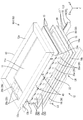
- FIG. Rear view of television receiver TV and liquid crystal display device 10 The exploded perspective view which shows schematic structure of the liquid crystal display unit LDU which comprises the liquid crystal display device 10.
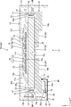
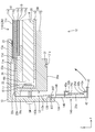
- FIG. Sectional drawing which shows the cross-sectional structure along the short side direction of the liquid crystal display device 10.
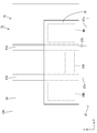
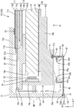
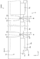
- 4 is a cross-sectional view of the main part of the backlight device 12 in which the vicinity of one LED unit LU is enlarged (showing a state where the mounting member 40 is in the second position). Sectional drawing of the principal part which shows the state by which the attachment member 40 is made into the 1st position.
- FIG. 7 is a cross-sectional view of the liquid crystal display device 210 according to Embodiment 3 along the short side direction, and is a cross-sectional view of the main part of the liquid crystal display device 210 in which the vicinity of one LED unit LU is enlarged (the attachment member 240 is a first member); (Shows the status of position 2)
- Embodiment 1 will be described with reference to the drawings.
- a liquid crystal display device an example of a display device 10 is illustrated.
- a part of each drawing shows an X-axis, a Y-axis, and a Z-axis, and each axis direction is drawn in a common direction in each drawing.
- the Y-axis direction coincides with the vertical direction
- the X-axis direction coincides with the horizontal direction.
- the vertical direction is used as a reference for upper and lower descriptions.
- the television receiver TV has a liquid crystal display unit LDU, various substrates PWB, MB, CTB attached to the back side (back side) of the liquid crystal display unit LDU, and the back side of the liquid crystal display unit LDU.
- a cover member CV attached to cover each main substrate PWB, MB, CTB, and a stand ST, and the display surface of the liquid crystal display unit LDU along the vertical direction (Y-axis direction) by the stand ST Is held by.
- the liquid crystal display device 10 according to the present embodiment is obtained by removing at least a configuration for receiving a television signal (such as a tuner portion of the main board MB) from the television receiver TV having the above-described configuration. As shown in FIG.
- the liquid crystal display unit LDU has a horizontally long rectangular shape (rectangular shape, longitudinal shape) as a whole, and includes a liquid crystal panel 11 that is a display panel and a backlight device 12 that is an external light source. These are configured to be integrally held by the outer frame 13 and the housing member 30 which are appearance members constituting the appearance of the liquid crystal display device 10.
- a pair of stand attachment members STA extending along the Y-axis direction are attached to the back surface of the liquid crystal display device 10 at two positions separated in the X-axis direction.
- These stand attachment members STA have a substantially channel shape with a cross-sectional shape opened to the accommodation member 30 side, and a pair of support columns STb in the stand ST are inserted into a space held between the stand members 30. It has become.
- a wiring member (such as an electric wire) connected to the LED substrate 18 (light source substrate) of the backlight device 12 is passed through the space in the stand attachment member STA.
- the stand ST includes a pedestal part STa that is parallel to the X-axis direction and the Z-axis direction, and a pair of column parts STb that rise from the pedestal part STa along the Y-axis direction.
- the cover member CV is made of synthetic resin, and is attached so as to cover about half of the lower side shown in FIG. 2 on the back surface of the liquid crystal display device 10 while traversing the pair of stand attachment members STA in the X-axis direction. Yes. Between the cover member CV and the liquid crystal display device 10, there is a component storage space in which components such as various substrates PWB, MB, and CTB described below can be stored.
- the various substrates PWB, MB, and CTB include a power supply substrate PWB, a main substrate MB, and a control substrate CTB.
- the power supply substrate PWB can be said to be a power supply source of the liquid crystal display device 10, and can supply driving power to the other substrates MB and CTB, the LED 17 (light source) of the backlight device 12, and the like. The Therefore, it can be said that the power supply substrate PWB also serves as the “LED drive substrate for driving the LED 17”.
- the main board MB has at least a tuner unit capable of receiving a television signal and an image processing unit (not shown) for processing the received television signal, and controls the processed image signal as follows. Output to the substrate CTB is possible.
- the main board MB receives an image signal from the image reproduction device when the liquid crystal display device 10 is connected to an external image reproduction device (not shown). It can be processed and output to the control board CTB.
- the control board CTB has a function of converting an image signal input from the main board into a liquid crystal driving signal and supplying the converted liquid crystal driving signal to the liquid crystal panel 11.
- the liquid crystal display unit LDU constituting the liquid crystal display device 10 has a main component between an outer frame 13 constituting the front side appearance and a housing member 30 constituting the rear side appearance. It is supposed to be housed in the space held by The housing member 30 includes a heat radiating member 19 and a chassis 14 which will be described later.
- the main components housed in the outer frame 13 and the housing member 30 include at least the liquid crystal panel 11, the optical member 15 (optical sheet), the light guide plate 16, the inner frame 22 (panel support member), and the LED unit LU. It is included.
- the liquid crystal panel 11, the optical member 15, and the light guide plate 16 are held in a state of being sandwiched between the outer frame 13 on the front side and the accommodating member 30 on the back side in a state of being stacked on each other.
- the backlight device 12 includes an inner frame 22, a light guide plate 16, an LED unit LU, and a chassis 14 (accommodating member 30).
- the liquid crystal panel 11, the optical member 15, and the outer frame 13 are connected to the liquid crystal display unit LDU.
- the configuration is excluded.
- a pair of LED units LU constituting the backlight device 12 are arranged so as to sandwich the light guide plate 16 from both sides in the short side direction (Y-axis direction).
- the LED unit LU includes an LED 17 that is a light source, an LED substrate 18 on which the LED 17 is mounted, and a heat dissipation member 19 to which the LED substrate 18 is attached.
- the heat radiating member 19 according to the present embodiment constitutes a part of the LED unit LU and a part of the housing member 30.
- the liquid crystal panel 11 has a horizontally long rectangular shape when seen in a plan view, as shown in FIG.
- the liquid crystal panel 11 has a configuration in which a pair of glass substrates 11a and 11b having excellent translucency are bonded together with a predetermined gap therebetween, and liquid crystal is sealed between the substrates 11a and 11b.
- the front side front side
- the back side rear side
- the array substrate 11b is the array substrate 11b.
- the array substrate 11b is provided with a switching element (for example, a thin film transistor: TFT) connected to a source wiring and a gate wiring orthogonal to each other, a pixel electrode connected to the switching element, an alignment film, and the like. .
- a switching element for example, a thin film transistor: TFT
- TFT thin film transistor
- a large number of TFTs and pixel electrodes are arranged side by side on the array substrate 11b, and a large number of TFTs and pixel electrodes are arranged around the TFTs and pixel electrodes so as to surround a gate wiring and a source wiring in a lattice shape. It is installed.
- the gate wiring and the source wiring are connected to the gate electrode and the source electrode of the TFT, respectively, and the pixel electrode is connected to the drain electrode of the TFT.
- the array substrate 11b is provided with capacitor wirings (auxiliary capacitor wirings, storage capacitor wirings, Cs wirings) that are parallel to the gate wirings and overlap the pixel electrodes in plan view. Are arranged alternately in the Y-axis direction.
- the CF substrate 11a is provided with a color filter in which colored portions such as R (red), G (green), and B (blue) are arranged in a predetermined arrangement, a counter electrode, and an alignment film. .
- a polarizing plate (not shown) is disposed outside each of the substrates 11a and 11b.
- the array substrate 11b is formed larger in size in plan view than the CF substrate 11a as shown in FIG.
- the array substrate 11b is arranged in such a manner that its end protrudes outward from the end of the CF substrate 11a.
- the array substrate 11b is formed to be slightly larger than the CF substrate 11a so that its outer peripheral end protrudes outside the outer peripheral end of the CF substrate 11a over the entire periphery.
- the pair of long-side end portions constituting the outer peripheral end portion of the array substrate 11b the long-side end portion on the control substrate CTB side (front side shown in FIG. 3, left side shown in FIG.
- a flexible substrate 26a (flexible wiring) is connected to each source side terminal portion.
- a plurality of flexible substrates 26a are intermittently arranged in the X-axis direction (that is, the direction along the long side end of the array substrate 11b). Each flexible substrate 26a protrudes outward along the Y-axis direction from the end portion on the long side of the array substrate 11b.
- one of the pair of short side end portions (the back side shown in FIG. 3) constituting the outer peripheral end portion of the array substrate 11b is extended from the above-described gate wiring and capacitance wiring.
- a plurality of gate-side terminal portions (not shown) that are rotated are provided.
- a flexible substrate 26b (flexible wiring) is connected to each gate side terminal portion.
- a plurality of flexible substrates 26b are intermittently arranged in the Y-axis direction, that is, in the direction along the short side end of the array substrate 11b. Each flexible substrate 26b protrudes outward along the X-axis direction from the short side end of the array substrate 11b.
- Each of the flexible boards 26a and 26b includes a film-like base material made of a synthetic resin material (for example, polyimide resin) having insulating properties and flexibility, and a driver for driving a liquid crystal mounted on the base material. ing. A large number of wiring patterns (not shown) are formed on the base material of each flexible substrate 26a, 26b, and a driver mounted near the center of the base material is connected to the wiring pattern.
- SOF System on Film
- One end of the flexible substrate 26a is pressure-bonded to the source side terminal provided on the panel surface 11e of the array substrate 11b via an anisotropic conductive film (ACF), and the other end is connected.
- the end portion is crimped and connected via a anisotropic conductive film (ACF) to a terminal portion (not shown) of a source-side printed board 25a (driving board) described later.
- the printed board 25a is connected to the control board CTB described above via a wiring member (not shown).
- the printed circuit board 25a transmits signals (scanning signals to the gate wiring, data signals to the source wiring, capacitance signals to the capacity wiring, etc.) input from the control board CTB to the flexible board 26a.
- the printed circuit board 25a has a long shape (band shape).
- two printed boards 25a are used, and these are connected to each flexible board 26a so as to be aligned with each other.
- the length of one printed circuit board 25 a is set to about half of the long side of the liquid crystal panel 11.
- one end of the flexible substrate 26b is crimped and connected to a gate side terminal provided on one panel surface 11e of the array substrate 11b via an anisotropic conductive film (ACF).
- ACF anisotropic conductive film
- the other end is crimped and connected via a anisotropic conductive film (ACF) to a terminal portion (not shown) of a gate side printed circuit board 25b (driving board) described later.
- the printed circuit board 25b has a long shape (band shape).
- two printed boards 25b are used, and these are connected to each flexible board 26b so as to be aligned with each other.
- the length of one printed circuit board 25b is set to about half the short side of the liquid crystal panel 11.
- the array substrate 11b is formed with a relay wiring (not shown) connecting the source side terminal portion and the gate side terminal portion.
- a signal (scanning signal to the gate wiring, capacitance signal to the capacitance wiring, etc.) input from the control board CTB is transmitted to the gate side terminal portion, the flexible board 26b, and the printed board 25b through the relay wiring.
- the liquid crystal panel 11 displays an image on the display surface 11c based on a signal input from the control board CTB.
- the printed circuit boards 25 a and 25 b are attached to the housing member 30 via the attachment member 40.
- the manner of attaching the printed board 25a to the housing member 30 and the attachment member 40 will be described later. Further, when collectively referring to the printed boards 25a and 25b, it is called a printed board 25 (driving board), and when collectively referring to the flexible boards 26a and 26b, it is called a flexible board 26 (flexible wiring).
- the liquid crystal panel 11 is placed on the front side (light emitting side) of the optical member 15 to be described later.
- the back surface of the liquid crystal panel 11 (the outer surface of the polarizing plate on the back side) is in close contact with the optical member 15 with almost no gap. This prevents dust and the like from entering between the liquid crystal panel 11 and the optical member 15.
- the display surface (front plate surface) 11c of the liquid crystal panel 11 has a display area on the center side of the screen where images can be displayed, and a frame shape (frame shape) surrounding the display area on the outer peripheral edge side of the screen. It consists of a non-display area.
- each terminal part and the flexible substrate 26 described above are arranged in a non-display area.
- the optical member 15 has a horizontally long rectangular shape when viewed from the same plane as the liquid crystal panel 11, and the size (short side dimension and long side dimension) is the same as that of the liquid crystal panel 11. Is done.
- the optical member 15 is placed on the front side (light emitting side) of the light guide plate 16 to be described later, and is sandwiched between the liquid crystal panel 11 described above and the inner frame 22 disposed on the front side of the light guide plate 16. It is arranged in the state.
- Each of the optical members 15 is in the form of a sheet and three are stacked on top of each other.
- the diffusion sheet 15a, the lens sheet (prism sheet) 15b, and the reflective polarizing sheet 15c are sequentially formed from the back side (light guide plate 16 side). Note that the three sheets 15a, 15b, and 15c have substantially the same size in a plan view.
- the outer frame 13 (frame) that holds the liquid crystal panel 11 from the front side and constitutes the appearance member will be described.
- the outer frame 13 is made of, for example, a metal such as aluminum, and has higher mechanical strength (rigidity) and thermal conductivity than a case where it is made of a synthetic resin.
- the outer frame 13 has a horizontally long frame shape as a whole so as to surround a display area on the display surface 11 c of the liquid crystal panel 11.
- the outer frame 13 includes a panel pressing portion 13a that is parallel to the display surface 11c of the liquid crystal panel 11 and presses the liquid crystal panel 11 from the front side, and a side wall portion 13b that protrudes from the outer peripheral side portion of the panel pressing portion 13a toward the back side.
- the cross-sectional shape is substantially L-shaped.
- the panel pressing portion 13a forms a horizontally long frame shape following the outer peripheral end portion (non-display area, frame portion) of the liquid crystal panel 11, and presses the outer peripheral end portion of the liquid crystal panel 11 from the front side over almost the entire circumference. Is possible.
- a buffer material 23 is interposed between the panel pressing portion 13 a and the liquid crystal panel 11.
- the outer surface of the panel pressing portion 13a facing the front side (the surface opposite to the surface facing the liquid crystal panel 11) is exposed to the outside on the front side of the liquid crystal display device 10 like the display surface 11c of the liquid crystal panel 11.
- the front surface of the liquid crystal display device 10 is configured together with the display surface 11 c of the panel 11.
- the side wall portion 13b has a plate shape extending from the outer peripheral end of the panel pressing portion 13a to the back side (housing member 30 side).
- the side wall portion 13b surrounds the backlight device 12 (the inner frame 22, the housing member 30) over the entire circumference.
- the side wall portion 13 b has an outer surface along the circumferential direction of the liquid crystal display device 10 exposed to the outside in the circumferential direction of the liquid crystal display device 10, and constitutes a top surface, a bottom surface, and both side surfaces of the liquid crystal display device 10.
- the side wall 13b is formed with a screw insertion hole 13c through which the screw member SM is inserted from the side.
- the screw insertion holes 13c are formed at both ends in the X-axis direction on each long side of the side wall portion 13b.
- an attachment member 40 is rotatably attached to an end surface of the side wall portion 13b opposite to the panel pressing portion 13a, that is, the back surface 13d of the side wall portion 13b.
- the attachment structure of the attachment member 40 in the side wall part 13b will be described later.
- the light guide plate 16 is made of a synthetic resin material (for example, acrylic resin such as PMMA or polycarbonate) having a refractive index sufficiently higher than that of air and substantially transparent (excellent translucency).
- the light guide plate 16 has a horizontally long rectangular shape when viewed in a plan view, as in the liquid crystal panel 11 and the optical member 15, and has a plate shape that is thicker than the optical member 15.
- the long side direction on the surface coincides with the X-axis direction
- the short side direction coincides with the Y-axis direction
- the plate thickness direction orthogonal to the main surface coincides with the Z-axis direction.
- the light guide plate 16 is laminated on the back side of the optical member 15 and is disposed so as to be sandwiched between the optical member 15 and the chassis 14. As shown in FIG. 4, the light guide plate 16 has at least a short side dimension larger than each short side dimension of the liquid crystal panel 11 and the optical member 15, and both end portions in the short side direction (long side direction). Are arranged so as to protrude outward from both end portions of the liquid crystal panel 11 and the optical member 15 (so as to be non-overlapping in a plan view).
- the light guide plate 16 is disposed in a form sandwiched in the Y-axis direction by a pair of LED units LU disposed on both sides in the short side direction, and light from the LED 17 is respectively received at both ends in the short side direction. It has been introduced.
- the light guide plate 16 has a function of raising and emitting the light from the LED 17 introduced from both ends in the short side direction so as to face the optical member 15 side (front side) while propagating inside.
- the surface facing the front side is a light emitting surface 16 a that emits internal light toward the optical member 15 and the liquid crystal panel 11.
- a light emitting surface 16 a that emits internal light toward the optical member 15 and the liquid crystal panel 11.
- both end faces on the long side that are long along the X-axis direction are LEDs 17 ( The LED board 18) and the LED board 18) are opposed to each other with a predetermined space therebetween, and these form a pair of light incident surfaces 16b on which light emitted from the LEDs 17 is incident.
- the light incident surface 16b is a surface parallel to the X-axis direction and the Z-axis direction (the main plate surface of the LED substrate 18), and is a surface substantially orthogonal to the light emitting surface 16a. Further, the alignment direction of the LED 17 and the light incident surface 16b coincides with the Y-axis direction and is parallel to the light emitting surface 16a.
- the back side of the light guide plate 16, that is, the surface opposite to the light emitting surface 16a (the surface facing the chassis 14) 16c reflects light emitted from the surface 16c to the outside outside as shown in FIG.
- a reflection sheet 20 that can be raised to the front side is provided so as to cover almost the entire region.
- the reflection sheet 20 is disposed in a form sandwiched between the chassis 14 and the light guide plate 16.
- the reflection sheet 20 is made of a synthetic resin and has a white surface with excellent light reflectivity.
- the reflection sheet 20 has a short side dimension larger than the short side dimension of the light guide plate 16, and both ends thereof are arranged to protrude closer to the LED 17 than the light incident surface 16 b of the light guide plate 16.
- Light that travels obliquely from the LED 17 toward the chassis 14 can be efficiently reflected by the projecting portion of the reflection sheet 20 and directed toward the light incident surface 16 b of the light guide plate 16.
- at least one of the light exit surface 16a and the opposite surface 16c of the light guide plate 16 has a reflection part (not shown) for reflecting internal light or a scattering part (not shown) for scattering internal light.
- a reflection part for reflecting internal light
- a scattering part not shown
- the inner frame 22 (panel support member) is formed in a horizontally long frame shape (frame shape) like the outer frame 13 as a whole, and is made of synthetic resin and has a surface. For example, it is set as the form which exhibits black, and shall have light-shielding property.
- the inner frame 22 can hold the outer peripheral end of the light guide plate 16 and the light source mounting portion 19a of the heat radiating member 19 from the front side, and can receive the outer peripheral end of the liquid crystal panel 11 and the optical member 15 from the back side over almost the entire circumference. It is configured. As shown in FIG.
- the panel support surface 22 a that receives the surface 11 d opposite to the display surface 11 c of the liquid crystal panel 11 is the front side with respect to the inner portion that receives the outer peripheral end of the optical member 15. It is supposed to protrude in a staircase shape.
- the inner frame 22 has a wiring support portion 22b protruding from the panel support surface 22a on the outer side.
- the wiring support portion 22b has a protruding end surface 22c arranged on the same plane as the one panel surface 11e provided with the source side terminal portion and the gate side terminal portion, and supports the flexible substrates 26a and 26b. Is done.
- the LED 17 constituting the LED unit LU has a configuration in which an LED chip is sealed with a resin material on a substrate portion fixed to the LED substrate 18.
- the LED chip mounted on the substrate unit has one main emission wavelength, and specifically, one that emits blue light in a single color is used.
- the resin material that seals the LED chip is dispersed and blended with a phosphor that emits a predetermined color when excited by the blue light emitted from the LED chip, and generally emits white light as a whole. It is said.
- a yellow phosphor that emits yellow light for example, a green phosphor that emits green light, and a red phosphor that emits red light are used in appropriate combination, or any one of them is used. It can be used alone.
- the LED 17 is a so-called top surface light emitting type in which a surface opposite to the mounting surface with respect to the LED substrate 18 (a surface facing the light incident surface 16b of the light guide plate 16) is a main light emitting surface.
- the heat dissipating member 19 constituting the LED unit LU is made of a metal having excellent thermal conductivity such as aluminum, for example, and as shown in FIGS. 3 and 4, a light source mounting portion 19a to which the LED substrate 18 is mounted,
- the surface (the plate surface facing the chassis 14 side) is in contact with the plate surface of the chassis 14 and the back surface (the surface opposite to the liquid crystal panel 11) is exposed to the back side of the liquid crystal display device 10 as a heat radiating portion 19b.
- These have a substantially L-shaped bent shape in cross section.
- the length of the heat radiation member 19 is approximately the same as the length of the chassis 14 described above.
- the light source mounting portion 19a has a plate shape parallel to the plate surface of the LED substrate 18 and the light incident surface 16b of the light guide plate 16, and the long side direction is the X-axis direction and the short side direction. Are coincident with the Z-axis direction and the thickness direction is coincident with the Y-axis direction.
- the LED board 18 is attached to the inner plate surface of the light source mounting portion 19a, that is, the plate surface facing the light guide plate 16 side.
- the long side dimension of the light source mounting portion 19 a is substantially the same as the long side dimension of the LED substrate 18, the short side dimension is larger than the short side dimension of the LED substrate 18.
- both end portions in the short side direction of the light source mounting portion 19a protrude outward from the both end portions of the LED substrate 18 along the Z-axis direction.
- the outer plate surface of the light source mounting portion 19a that is, the plate surface opposite to the plate surface to which the LED substrate 18 is mounted, is opposed to a side wall portion 13b of the outer frame 13 described later.
- the light source mounting portion 19 a is disposed so as to be interposed between the side wall portion 13 b of the outer frame 13 and the light guide plate 16.
- the light source mounting portion 19a is formed with a screw groove (not shown) into which the screw member SM is screwed at a position corresponding to the screw insertion hole 13c of the side wall portion 13b.
- the heat dissipating part 19 b has a plate shape parallel to the plate surface of the chassis 14.
- the long side direction is the X-axis direction
- the short side direction is the Y-axis direction
- the thickness direction is These coincide with the Z-axis direction.
- the heat dissipating part 19b is configured to protrude inward along the Y-axis direction from the back side end of the light source mounting part 19a, that is, the end on the chassis 14 side.
- the light source mounting portion 19a is arranged on the front side (the liquid crystal panel 11 side) with respect to the chassis 14, while the heat radiating portion 19b is arranged on the back side (the side opposite to the liquid crystal panel 11) with respect to the chassis 14. Yes.
- the heat dissipating part 19b has a long side dimension substantially the same as that of the light source attaching part 19a, while its short side dimension and thickness dimension are larger than the light source attaching part 19a, and has a high heat dissipation configuration. ing.
- the heat dissipating part 19b has a back surface, that is, a back surface 30a (surface opposite to the liquid crystal panel 11) of the housing member 30 where the side close to the light source attaching part 19a is far from the light source attaching part 19a (the protruding end of the heat dissipating part 19b). Side), the height of the back surface increases stepwise.
- the heat dissipating part 19b is provided with a recess 31 into which the mounting member 40 is fitted in a stepped portion of the back surface 30a of the housing member 30. The configuration of the recess 31 will be described later.
- the chassis 14 is made of a metal plate material, and has a horizontally long rectangular shape as a whole so as to cover the light guide plate 16 over almost the entire region from the back side.
- a plate surface on the front side of the heat radiating portion 19 b of the heat radiating member 19 is arranged in a state where the entire surface is in surface contact.
- the chassis 14 which is a metal member having a larger heat capacity than the heat radiating member 19. Heat dissipation can be further promoted by utilizing the heat capacity of the chassis 14.
- the chassis 14 is assembled with the heat radiating member 19 to form a housing member 30.
- the housing member 30 is arranged with a pair of heat radiating members 19 facing each other with the heat radiating portions 19 b facing inward, and both long side edges of the chassis 14 are arranged on the respective heat radiating members 19. It is configured by being arranged on the surface of the heat dissipating part 19b.
- the housing member 30 has a U shape in a cross-sectional view in the short side direction (Y-axis direction) of the chassis 14, and forms a space for housing main components of the backlight device 12.
- the housing member 30 includes a metal heat radiating member 19 and a chassis 14, and has higher mechanical strength (rigidity) than a case where the housing member 30 is made of synthetic resin.
- the assembly structure of the heat dissipation member 19 and the chassis 14 includes a structure in which the chassis 14 is sandwiched between the heat dissipation member 19 and the outer frame 13 together with other components by attaching the heat dissipation member 19 to the outer frame 13.
- a configuration in which the chassis 14 and the heat radiating portion 19b are fixed and assembled by a known method such as screwing can be exemplified.
- the configuration related to the mounting member 40 and the manner of mounting the printed circuit boards 25a and 25b to the housing member 30, which are the main parts of the present embodiment, will be described in detail.
- the attachment aspect of the printed circuit board 25a and the printed circuit board 25b is made the same, In the following description, the attachment aspect of the printed circuit board 25a is demonstrated, and description is abbreviate
- the mounting manner of the mounting member 40 and the printed circuit board 25a is a symmetrical configuration, and in the following description, the configuration of the left end ( 5), and the description of the configuration of the right end is omitted.
- the side wall 13 b is provided with a groove 33 extending on the back surface 13 d in the rotation direction of the mounting member 40 (the thickness direction of the side wall 13 b, the Y-axis direction).
- the groove portion 33 is aligned with the recess portion 31 provided in the housing member 30 in the X-axis direction.
- the groove portion 33 has a pair of side surface portions 33a and 33a and a bottom surface portion 33b.
- the side surface portion 33 a has a curved shape extending along the side surface of the rotation shaft portion 41.
- the bottom surface portion 33b is a surface parallel to the back surface 13d of the side wall portion 13b as shown in FIG.
- the bottom surface portion 33 b is provided with a bearing portion 34 that supports the rotation shaft portion 41 of the mounting member 40 so as to be recessed from the bottom surface portion 33 b along the shape of the spherical crown of the rotation shaft portion 41.
- the recess 31 is formed such that the back surface 30a of the housing member 30 is recessed in a shape along the outer peripheral surface of the fitting portion 43 described later. In the recess 31, a portion that opens to the back surface 30 a of the housing member 30 is configured to be larger than the distal end portion of the fitting portion 43.
- the recess 31 is formed with a locking projection 31 a that protrudes inward from the opening edge and engages with the flange portion of the fitting portion 43.
- the mounting member 40 is made of synthetic resin and has an insulating property.
- the attachment member 40 includes a printed circuit board 25 a between a base portion 45 having a substantially L-shaped prism shape, a rotating shaft portion 41 provided on one end side of the base portion 45, and the base portion 45. And a fitting portion 43 that is provided on the other end side of the base portion 45 and is fitted to the containing member 30 (recessed portion 31).
- the base 45 is configured such that one end portion side extends along the printed circuit board 25a and the other end side rises in a direction orthogonal to the printed circuit board 25a in a state where the printed circuit board 25a is accommodated in the accommodating portion 42.
- Two attachment members 40 are provided for each printed board 25a. In the five flexible boards 26a connected to one printed board 25a, the flexible boards 26a disposed on both ends are provided. These are arranged corresponding to the positions between the adjacent flexible substrate 26a.
- the rotation shaft portion 41 has a spherical shape and is a portion that is rotatably attached to the side wall portion 13 b.
- the diameter of the rotation shaft portion 41 is larger than the width dimension of the base portion 45.
- the rotating shaft portion 41 is prevented from slipping in a direction (downward) perpendicular to the groove portion 33 by the pair of side surface portions 33a and 33a, and the groove portion 33 extends by the inner peripheral surface of the bearing portion 34. It is configured to be prevented from coming off in the (Y-axis direction). With such a configuration, the rotation shaft portion 41 is pushed into the bearing portion 34 so that the rotation shaft portion 41 is attached to the bearing portion 34 and the center of the rotation shaft portion 41 is centered on the rotation shaft. As a result, the mounting member 40 is turned.
- the accommodating portion 42 is a portion for locking the printed circuit board 25a, and a pair of locking pieces 42a for locking the printed circuit board 25a so as to sandwich the one end 25c and the other end 25d of the printed circuit board 25a. 42a.
- the locking piece 42 a is disposed on the housing member 30 side with respect to the base 45 in a state where the printed circuit board 25 a is attached to the housing member 30. As shown in FIG. 7, the locking piece 42 a is configured to lock a portion between the adjacent flexible boards 26 a in the printed board 25 a.
- the pair of locking pieces 42a and 42a are tapered surfaces whose end faces 42b and 42b that face each other become narrower in the direction in which the printed circuit board 25a is accommodated (direction closer to the base 45). In the pair of locking pieces 42a and 42a, the narrowest part of the end faces 42b and 42b facing each other is smaller than the width of the printed circuit board 25a, that is, the dimension from the one end 25c to the other end 25d. Somewhat
- the fitting portion 43 is a portion that is fixed to the back surface 30 a of the housing member 30, and is fitted to the concave portion 31 of the housing member 30 in the rotation direction of the mounting member 40.
- the fitting portion 43 has a flange portion that protrudes outwardly from the base portion 45 in a flange shape, and has a tapered shape in which the outer surface of the flange portion is tapered.
- the diameter of the flange portion is larger than the inner diameter of the locking protrusion 31a of the recess 31, and the flange portion is inserted into the locking projection 31a so as to be engageable with the locking projection 31a.
- the attachment member 40 is rotatable between a first position shown in FIG. 6 and a second position shown in FIG.
- the attachment member 40 is arranged such that one end portion side of the base portion 45 is arranged along the extending direction (Z-axis direction) of the side wall portion 13b at the first position, while one end of the base portion 45 is arranged at the second position.
- the part side is arranged at a position (position along the Y-axis direction) rotated 90 degrees with respect to the extending direction of the side wall part 13b.
- the printed circuit board 25a is locked to the mounting member 40 as shown in FIG.
- the accommodating portion 42 allows the printed circuit board 25a to be placed in a state where the printed circuit board 25a connected to the flexible circuit board 26a hangs down by its own weight at the first position of the mounting member 40. It can be accommodated.
- the operator then inserts the printed circuit board 25a between the pair of locking pieces 42a and 42a from the inside while visually recognizing the hand from the side of the outer frame 13, and stores (locks) the printed board 25a in the storage portion 42. To do.
- the attachment member 40 is rotated from the first position in the direction of the arrow shown in FIG. 6 with respect to the side wall portion 13b.
- the printed circuit board 25a is locked in the accommodating portion 42, and the attachment member 40 is rotated from the first position while bending the flexible circuit board 26a.
- the base 45 interferes with the pair of side surfaces 33a and 33a, and the mounting member 40 intersects with the rotation direction. Movement is restricted. For this reason, even if it is a case where the position of the recessed part 31 of the accommodating member 30 cannot be visually recognized from an operator, the position of the fitting part 43 and the recessed part 31 shall match in a 2nd position.
- the attachment member 40 is rotated to the second position, and the fitting portion 43 is fitted (fixed) to the concave portion 31 of the housing member 30.
- the fitting portion 43 is fitted (fixed) to the concave portion 31 of the housing member 30.
- the flange portion of the fitting portion 43 is engaged with the engagement protrusion 31 a of the recess 31, and the fitting portion 43 is removed from the recess 31.
- the printed circuit board 25 a is positioned by the inner peripheral surface of the housing portion 42 and the attachment member 40 is attached to the housing member 30. In this way, the attachment of the printed circuit board 25a to the housing member 30 is completed.
- the liquid crystal display device 10 includes an LED 17, a liquid crystal panel 11 that performs display using the light of the LED 17, a printed board 25 that controls display driving of the liquid crystal panel 11, the liquid crystal panel 11 and the printed board 25.
- a flexible substrate 26 that is electrically connected to the liquid crystal panel 11; a housing member 30 that is disposed on the opposite side of the display surface 11c that displays the liquid crystal panel 11;
- a frame-shaped outer frame 13 that holds at least the liquid crystal panel 11 between the member 30 and a panel pressing portion 13a that is disposed on the display surface 11c side and presses the liquid crystal panel 11 from the display surface 11c side.
- the outer frame 13 having a side wall portion 13b extending from the panel pressing portion 13a toward the housing member 30 and the side wall portion 13b.
- attachment member 40 which attaches the printed circuit board 25 with respect to the accommodation member 30, and is attached in the 1st position which latches the printed circuit board 25, and the state which latched the printed circuit board 25, It is possible to rotate between the second position fixed to the surface 30a opposite to the liquid crystal panel 11 of the housing member 30 by rotating with respect to the side wall portion 13b while bending the flexible substrate 26 from the position.
- a mounting member 40
- the attachment member 40 that attaches the printed circuit board 25 to the housing member 30 can be rotated between the first position and the second position. For this reason, even when it is a case where the printed circuit board 25 is attached with respect to the accommodation member 30 in the state where it is difficult to visually recognize the surface 30a on the opposite side to the liquid crystal panel 11 of the accommodation member 30, the 1st position which latches the printed circuit board 25. Then, the operation of locking the printed circuit board 25 to the attachment member 40 is performed in a state where the hand can be seen, and the attachment member 40 is turned to the second position by rotating the attachment member 40 with respect to the side wall portion 13b.
- the printed circuit board 25 can be suitably attached to the back side of the housing member 30 even in the large model liquid crystal display device 10 in which the reversing operation during the assembly of the liquid crystal display device 10 is particularly difficult.
- attachment of the printed circuit board 25 to the housing member 30 can be realized, which can contribute to narrowing the frame of the liquid crystal display device 10.
- the attachment member 40 is restricted from moving in the direction intersecting with the rotation direction between the first position and the second position. According to such a configuration, the workability of the work of fixing the mounting member 40 to the surface 30a opposite to the liquid crystal panel 11 of the housing member 30 is further improved.
- the attachment member 40 has a spherical rotation shaft portion 41 that is rotatably attached to the side wall portion 13b, and the side wall portion 13b has a panel pressing portion 13a and A bearing portion 34 that pivotally supports the rotation shaft portion 41 is provided on the opposite surface 30a.
- the structure which attaches the attachment member 40 with respect to the side wall part 13b with a simple structure so that rotation is possible is realizable.
- the side wall portion 13b has a groove portion 33 extending on the surface 13d opposite to the panel pressing portion 13a in the rotation direction of the mounting member 40, and has a pair of side surface portions 33a and 33a and a bottom surface portion.
- the groove part 33 having 33 b is provided, and the bearing part 34 is provided on the bottom surface part 33 b of the groove part 33.
- the side surface portion 33a of the groove portion 33 may restrict movement of the mounting member 40 in a direction intersecting with the rotation direction between the first position and the second position. it can.
- the attachment member 40 has a portion fixed to the surface 30 a opposite to the liquid crystal panel 11 of the accommodation member 30 fitted in the rotation direction of the attachment member 40 with respect to the accommodation member 30. It is set as the fitting part 43 to match. According to such a configuration, by rotating the attachment member 40 from the first position to the second position, the attachment member 40 can be fixed to the housing member 30 by the fitting portion 43. Furthermore, the workability of attaching the printed circuit board 25 to the housing member 30 is excellent.
- the attachment member 40 has a portion 42 that holds the printed circuit board 25 as a housing portion 42 that houses the printed circuit board 25, and the housing portion 42 includes a base 45 and a base 45.
- a pair of locking pieces 42a and 42a are provided to lock the printed circuit board 25 with one end 25c and the other end 25d interposed therebetween. According to such a structure, the structure which latches the printed circuit board 25 with respect to the attachment member 40 with a simple structure is realizable.
- the accommodating portion 42 can accommodate the printed circuit board 25 in a state where the printed circuit board 25 connected to the flexible substrate 26 hangs down by its own weight at the first position. According to such a configuration, the printed circuit board 25 can be easily accommodated in the accommodating portion 42, and the workability of locking the printed circuit board 25 with respect to the attachment member 40 is excellent.
- a plurality of flexible boards 26 are connected in parallel to the printed board 25 along the one end portion 25c, and the locking pieces 42a are flexible boards adjacent to each other on the printed board 25. The part between 26 is locked. According to such a configuration, it is possible to avoid a situation in which the flexible substrate 26 and the attachment member 40 interfere with each other.
- the pair of locking pieces 42 a and 42 a are tapered surfaces whose end faces 42 b and 42 b face each other become narrower in the direction in which the printed circuit board 25 is accommodated. According to such a configuration, the printed circuit board 25 can be more easily accommodated in the accommodating portion 42, and the workability of the operation of locking the printed circuit board 25 with respect to the attachment member 40 is excellent.
- the frame-shaped inner frame 22 is provided between the liquid crystal panel 11 and the housing member 30 and has a panel support surface 22a that supports the surface 11d opposite to the display surface 11c of the liquid crystal panel 11.
- the flexible substrate 26 is connected to the liquid crystal panel 11 on one panel surface 11e of the liquid crystal panel 11, and the inner frame 22 protrudes from the panel support surface 22a, and the protruding end surface 22c is one panel.
- the wiring support portion 22b is disposed on the same plane as the surface 11e and supports the flexible substrate 26. According to such a configuration, by supporting the flexible substrate 26 with the wiring support portion 22b, it is possible to suppress an unexpected force from being applied to the connection portion between the liquid crystal panel 11 and the flexible substrate 26. And the reliability of the connection between the flexible substrate 26 and the flexible substrate 26 can be improved.
- the attachment member 40 is arranged along the extending direction of the side wall portion 13b at the first position, whereas the mounting member 40 is arranged along the extending direction of the side wall portion 13b at the second position. It is supposed to be arranged at a position rotated 90 degrees. According to such a configuration, the printed circuit board 25 can be attached to the housing member 30 with a simple structure, and the workability of attaching the printed circuit board 25 to the housing member 30 is further improved.
- the liquid crystal panel 11 is exemplified as the display panel.
- a display device can be applied to the liquid crystal display device 10 for various uses such as a display of a television or a personal computer, and is particularly suitable for a large screen.
- FIG. 2 A second embodiment of the present invention will be described with reference to FIG.
- the second embodiment is different from the first embodiment in the manner in which the mounting member 140 is attached to the side wall 113b and the configuration in which the mounting member 140 is rotatable with respect to the side wall 113b.
- the side wall 113b is provided with a screw groove 137 into which a small screw 136 is screwed on a side surface 113e facing the light source mounting portion 19a of the heat radiating member 19 at the end opposite to the panel pressing portion 13a.
- the thread groove 137 is aligned with the concave portion 31 provided in the housing member 30 in the X-axis direction.
- the mounting member 140 is made of a synthetic resin and has an insulating property.
- the attachment member 140 includes a base portion 145 having a substantially L-shaped plate shape in cross section, an attachment portion 147 provided on one end side of the base portion 145, and in the vicinity of the attachment portion 147, and one end portion from the attachment portion 147.
- the accommodating part 42 for accommodating the printed circuit board 25, and provided on the other end side of the base part 145 and fitted to the accommodating member 30 (recess 31).
- a fitting portion 43 to be joined is configured such that one end portion extends along the printed circuit board 25 and the other end portion rises in a direction intersecting with the printed circuit board 25 in a state where the printed circuit board 25 is accommodated in the accommodating section 42.
- the attachment portion 147 is an insertion hole through which the shaft portion of the small screw 136 can be inserted.
- the attachment member 140 is attached to the side wall portion 113b by causing the attachment portion 147 and the screw groove 137 to communicate with each other and screwing the small screw 136 to the side wall portion 113b.
- the rotating part 148 is a thin part in which the thickness of the base part 145 is reduced along the width direction (X-axis direction) of the base part 145.
- the base portion 145 has a plate shape and a thin portion is formed along the width direction (X-axis direction) of the base portion 145, the attachment member 140 is located between the first position and the second position. The movement in the direction intersecting with the rotation direction is restricted.
- the attachment member 140 includes an attachment portion 147 and a rotation portion 148 that are rotatably attached to the side wall portion 113b.
- the attachment member 140 is configured such that the attachment portion 147 is attached to the side wall portion 113b via the small screw 136 and rotates around the rotation portion 148 which is a thin portion. According to such a structure, the structure which attaches the attachment member 140 with respect to the side wall part 113b with a simple structure so that rotation is possible is realizable.
- Embodiment 3 A third embodiment of the present invention will be described with reference to FIG.
- FIG. the overlapping description about the same structure, an effect
- the housing member 230 has a back surface 30a, which is a surface 30a opposite to the liquid crystal panel 11, with a surface of the mounting member 240 opposite to the base 245 of the pair of locking pieces 42a, 42a and an adhesive layer 249 described later. It is set as the plane part which is surface-contacted. That is, unlike the first embodiment, the housing member 230 is not provided with a recess.
- the mounting member 240 is made of synthetic resin and has an insulating property.
- the mounting member 240 includes a base portion 245 having a substantially L-shaped prism shape, a rotating shaft portion 41 provided on one end side of the base portion 245, and a housing portion 42 that houses the printed board 25 between the base portion 245. , And an adhesive layer 249 provided on a surface opposite to the base 245 of the housing portion 42.
- the adhesive layer 249 is a portion fixed to the back surface 30a of the housing member 230, and is provided on each of the surface 30a of the housing member 230 opposite to the liquid crystal panel 11 and the pair of locking portions 42a and 42a. It is supposed to adhere.
- a part of the mounting member 240 that is fixed to the surface 30a opposite to the liquid crystal panel 11 of the housing member 230 is an adhesive layer 249. According to such a configuration, the attachment member 240 can be fixed to the housing member 230 with a simple configuration.
- the fitting portion and the adhesive layer are exemplified as the configuration of the portion where the mounting member is fixed to the surface of the housing member opposite to the display panel.
- the present invention is not limited to this. Absent.
- it may be fixed by means such as a clip, a double-sided tape, or a magnet, and the fixing means can be appropriately changed.
- the housing portion is exemplified as the configuration of the portion where the mounting member locks the drive substrate.
- the present invention is not limited to this.
- the locking means, the locking position on the printed circuit board, and the arrangement configuration of the locking position can be changed as appropriate.
- the housing member is exemplified by the heat radiation member and the chassis, but is not limited thereto.
- the housing member may be any member as long as it accommodates at least the light source, and may be configured only by the chassis.
- each printed circuit board 25a, 25b is attached to the housing member 30 by the attachment member 40 is illustrated, but only one of the printed circuit boards 25a, 25b is attached to the housing member 30. It may be attached. Further, the present invention includes a configuration in which either one of the printed boards 25a and 25b is not provided.
- a pair of LED units are arranged so as to face the ends on both long sides of the light guide plate.
- the present invention also includes a pair arranged so as to face the end portions on the short side.
- the present invention includes one LED unit disposed so as to face only one end of one long side or one short side of the light guide plate. Further, the present invention also includes a configuration in which three LED units are arranged so as to face each end of any three sides of the light guide plate.
- LED units LED substrates
- one LED unit or one LED unit for one side of the light guide plate is used. Three or more may be arranged.
- an LED is used as a light source, but other light sources such as an organic EL can be used.
- the edge light type backlight device including the light guide plate is illustrated, but the configuration of the backlight device can be changed as appropriate.
- the backlight device may be configured not to include a light guide plate but to directly supply light from the back surface to the liquid crystal panel (so-called direct type).
Landscapes
- Physics & Mathematics (AREA)
- Nonlinear Science (AREA)
- Engineering & Computer Science (AREA)
- Multimedia (AREA)
- Signal Processing (AREA)
- Mathematical Physics (AREA)
- Chemical & Material Sciences (AREA)
- Crystallography & Structural Chemistry (AREA)
- General Physics & Mathematics (AREA)
- Optics & Photonics (AREA)
- Liquid Crystal (AREA)
- Devices For Indicating Variable Information By Combining Individual Elements (AREA)
Abstract
液晶表示装置10は、LED17と、液晶パネル11と、プリント基板25と、フレキシブル基板26と、収容部材30と、パネル押さえ部13aと側壁部13bとを有する外側フレーム13と、側壁部13bに対して回動可能に取り付けられるとともに、プリント基板25を収容部材30に対して取り付ける取付部材40であって、プリント基板25を係止する第1の位置と、プリント基板25を係止した状態で、第1の位置からフレキシブル基板26を折り曲げつつ側壁部13bに対して回動して、収容部材30の液晶パネル11と反対側の面30aに対して固定される第2の位置と、の間で回動可能とされる取付部材40と、を備える。
Description
本発明は、表示装置、及びテレビ受信装置に関する。
近年、テレビ受信装置をはじめとする画像表示装置の表示素子は、従来のブラウン管から液晶パネルやプラズマディスプレイパネルなどの薄型表示素子を適用した薄型表示装置に移行しつつあり、画像表示装置の薄型化を可能としている。このような表示装置の一例として、下記特許文献1に記載されたものが知られている。
特許文献1では、平面表示素子(表示パネル)と、この平面表示素子の一主面側に少なくとも一部が位置する構造物と、平面表示素子に基端側が電気的に接続され、この平面表示素子から外側に突出するフレキシブル基板(駆動基板やフレキシブル配線)とを具備し、フレキシブル基板は、平面表示素子に対して一主面側に折り返された折り返し部と、この折り返し部の先端側に位置し、固着部材を介して構造物に固着される固着部とを備えているものが開示されている。
(発明が解決しようとする課題)
しかしながら、特許文献1では、固着部は、フレキシブル基板の可撓性に起因して、構造物の平面表示素子と反対側の面において、ある範囲に広がる領域に固着され得る。このため、固着部を所期の位置に固着する為には、構造物の平面表示素子と反対側の面を視認できる状態で構造物と固着部との位置合わせをする必要がある。
しかしながら、特許文献1では、固着部は、フレキシブル基板の可撓性に起因して、構造物の平面表示素子と反対側の面において、ある範囲に広がる領域に固着され得る。このため、固着部を所期の位置に固着する為には、構造物の平面表示素子と反対側の面を視認できる状態で構造物と固着部との位置合わせをする必要がある。
ところで、表示装置は、その組み付け態様として、構造物等からなる照明装置の上に表示パネルを積層するようにして組み付ける場合がある。このような場合には、固着部を構造物に対して固着する際に、構造物の平面表示素子と反対側の面を視認できる状態にするために、フレキシブル基板を構造物に対して固着する前の表示装置を反転する必要がある。すると、当該反転作業に伴って、駆動基板やフレキシブル配線が損傷する虞がある。
本発明は上記のような事情に基づいて完成されたものであって、組み付け中の表示装置を反転する必要がないために、駆動基板やフレキシブル配線が損傷する事態の発生が抑制された表示装置を提供することを目的とする。
(課題を解決するための手段)
本発明の表示装置は、光源と、前記光源の光を利用して表示を行う表示パネルと、前記表示パネルの表示駆動を制御する駆動基板と、前記表示パネルと前記駆動基板との間を電気的に接続する可撓性を備えたフレキシブル配線と、前記表示パネルの前記表示を行う表示面側とは反対側に配され、少なくとも前記光源を収容する収容部材と、前記収容部材との間で少なくとも前記表示パネルを挟み込む形で保持する枠状のフレームであって、前記表示面側に配されるとともに前記表示パネルを前記表示面側から押さえるパネル押さえ部と、前記パネル押さえ部から前記収容部材側に延びる側壁部と、を有するフレームと、前記側壁部に対して回動可能に取り付けられるとともに、前記駆動基板を前記収容部材に対して取り付ける取付部材であって、前記駆動基板を係止する第1の位置と、前記駆動基板を係止した状態で、前記第1の位置から前記フレキシブル配線を折り曲げつつ前記側壁部に対して回動して、前記収容部材の前記表示パネルと反対側の面に対して固定される第2の位置と、の間で回動可能とされる取付部材と、を備える。
本発明の表示装置は、光源と、前記光源の光を利用して表示を行う表示パネルと、前記表示パネルの表示駆動を制御する駆動基板と、前記表示パネルと前記駆動基板との間を電気的に接続する可撓性を備えたフレキシブル配線と、前記表示パネルの前記表示を行う表示面側とは反対側に配され、少なくとも前記光源を収容する収容部材と、前記収容部材との間で少なくとも前記表示パネルを挟み込む形で保持する枠状のフレームであって、前記表示面側に配されるとともに前記表示パネルを前記表示面側から押さえるパネル押さえ部と、前記パネル押さえ部から前記収容部材側に延びる側壁部と、を有するフレームと、前記側壁部に対して回動可能に取り付けられるとともに、前記駆動基板を前記収容部材に対して取り付ける取付部材であって、前記駆動基板を係止する第1の位置と、前記駆動基板を係止した状態で、前記第1の位置から前記フレキシブル配線を折り曲げつつ前記側壁部に対して回動して、前記収容部材の前記表示パネルと反対側の面に対して固定される第2の位置と、の間で回動可能とされる取付部材と、を備える。
上記の表示装置によれば、駆動基板を収容部材に対して取り付ける取付部材が、第1の位置と第2の位置との間で回動可能とされる。このため、収容部材の表示パネルと反対側の面を視認し難い状態で駆動基板を収容部材に対して取り付ける場合であっても、駆動基板を係止する第1の位置では、駆動基板を取付部材に係止する作業を、手元が見える状態で行うとともに、取付部材を側壁部に対して回動させて第2の位置とすることで、取付部材を収容部材の表示パネルと反対側の面に対して固定することができ、駆動基板を収容部材に対して取り付ける作業の作業性に優れる。
この結果、表示パネル側を視認し易い状態で表示装置を組み付けている場合において、駆動基板を収容部材に対して取り付ける際に、組み付け中の表示装置を反転させて、収容部材の表示パネルと反対側の面を視認し易い状態とする必要がなく、組み付け中の表示装置を反転させることに伴って、駆動基板やフレキシブル配線が損傷する事態の発生を抑制することができる。
この結果、表示パネル側を視認し易い状態で表示装置を組み付けている場合において、駆動基板を収容部材に対して取り付ける際に、組み付け中の表示装置を反転させて、収容部材の表示パネルと反対側の面を視認し易い状態とする必要がなく、組み付け中の表示装置を反転させることに伴って、駆動基板やフレキシブル配線が損傷する事態の発生を抑制することができる。
本発明の実施態様として、次の構成が好ましい。
(1)前記取付部材は、前記第1の位置と前記第2の位置との間の回動方向と交わる方向への移動が規制されている。このような構成によれば、より一層、取付部材を収容部材の表示パネルと反対側の面に対して固定する作業の作業性に優れる。
(1)前記取付部材は、前記第1の位置と前記第2の位置との間の回動方向と交わる方向への移動が規制されている。このような構成によれば、より一層、取付部材を収容部材の表示パネルと反対側の面に対して固定する作業の作業性に優れる。
(2)前記取付部材は、前記側壁部に対して回動可能に取り付けられる部分が、球状の回動軸部とされており、前記側壁部には、前記パネル押さえ部と反対側の面に、前記回動軸部を軸支する軸受け部が設けられている。このような構成によれば、簡易な構成で、取付部材を側壁部に対して回動可能に取り付ける構成を実現することができる。
(3)前記側壁部には、前記パネル押さえ部と反対側の面に、前記取付部材の回動方向に延びる溝部であって、一対の側面部と底面部とを有する溝部が設けられており、前記軸受け部は、前記溝部の前記底面部に設けられている。このような構成によれば、溝部の側面部が、取付部材の第1の位置と第2の位置との間の回動方向と交わる方向への移動を規制するものとすることができる。
(4)前記取付部材は、前記収容部材の前記表示パネルと反対側の面に対して固定される部分が、前記収容部材に対して、前記取付部材の回動方向に嵌合する嵌合部とされている。このような構成によれば、取付部材を第1の位置から第2の位置に回動させることにより、嵌合部による取付部材の収容部材に対する固定も実現することができ、より一層、駆動基板を収容部材に対して取り付ける作業の作業性に優れる。
(5)前記取付部材は、前記駆動基板を係止する部分が、当該駆動基板を収容する収容部とされており、前記収容部は、基部と、前記基部との間で前記駆動基板の一端部と他端部をそれぞれ挟み込む形で係止する一対の係止片と、を有している。このような構成によれば、簡易な構成で、取付部材に対して駆動基板を係止する構成を実現することができる。
(6)前記収容部は、前記第1の位置において、前記フレキシブル配線に接続された前記駆動基板が自重により垂れ下がった状態で、当該駆動基板を収容可能とされている。このような構成によれば、収容部に駆動基板を容易に収容することができ、取付部材に対して駆動基板を係止する作業の作業性に優れる。
(7)前記駆動基板には、前記一端部に沿って、複数の前記フレキシブル配線が並列して接続されており、前記係止片は、前記駆動基板において、互いに隣接する前記フレキシブル配線の間の部分を係止するものとされている。このような構成によれば、フレキシブル配線と取付部材とが干渉する事態を回避することができる。
(8)前記一対の係止片は、互いに向かい合う端面が、前記駆動基板を収容する方向に向かうにつれて幅が狭くなるテーパ面とされている。このような構成によれば、収容部に駆動基板を、より一層容易に収容することができ、取付部材に対して駆動基板を係止する作業の作業性に優れる。
(9)前記表示パネルと前記収容部材との間に配され、前記表示パネルの前記表示面とは反対側の面を支持するパネル支持面を有する枠状のパネル支持部材を更に備え、前記フレキシブル配線は、前記表示パネルの一のパネル面上で当該表示パネルに接続されており、前記パネル支持部材は、前記パネル支持面から突出し、その突出端面が前記一のパネル面と同一平面上に配されるとともに、前記フレキシブル配線を支持する配線支持部を有する。このような構成によれば、配線支持部でフレキシブル配線を支持することにより、表示パネルとフレキシブル配線との接続部分に不測の力が掛かることを抑制することができ、表示パネルとフレキシブル配線との接続の信頼性を向上することができる。
(10)前記取付部材は、前記第1の位置において、前記側壁部の延び方向に沿って配されるものとされる一方、前記第2の位置において、前記側壁部の前記延び方向に対して90度回動した位置に配されるものとされている。このような構成によれば、簡易な構成で、駆動基板を収容部材に対して取り付けることができ、より一層、駆動基板を収容部材に対して取り付ける作業の作業性に優れる。
また、前記表示パネルとしては液晶パネルを例示することができる。このような表示装置は液晶表示装置として、種々の用途、例えばテレビやパソコンのディスプレイ等に適用でき、特に大型画面用として好適である。
(発明の効果)
本発明によれば、駆動基板やフレキシブル配線が損傷する事態の発生が抑制された表示装置を提供することができる。
本発明によれば、駆動基板やフレキシブル配線が損傷する事態の発生が抑制された表示装置を提供することができる。
<実施形態1>
図面を参照して実施形態1を説明する。本実施形態では、液晶表示装置(表示装置の一例)10について例示する。なお、各図面の一部にはX軸、Y軸およびZ軸を示しており、各軸方向が各図面で共通した方向となるように描かれている。このうちY軸方向は、鉛直方向と一致し、X軸方向は、水平方向と一致している。また、特に断りがない限りは、上下の記載については鉛直方向を基準とする。
図面を参照して実施形態1を説明する。本実施形態では、液晶表示装置(表示装置の一例)10について例示する。なお、各図面の一部にはX軸、Y軸およびZ軸を示しており、各軸方向が各図面で共通した方向となるように描かれている。このうちY軸方向は、鉛直方向と一致し、X軸方向は、水平方向と一致している。また、特に断りがない限りは、上下の記載については鉛直方向を基準とする。
テレビ受信装置TVは、図1に示すように、液晶表示ユニットLDUと、液晶表示ユニットLDUの裏面側(背面側)に取り付けられる各種基板PWB,MB,CTBと、液晶表示ユニットLDUの裏面側に各主基板PWB,MB,CTBを覆う形で取り付けられるカバー部材CVと、スタンドSTとを備えてなり、スタンドSTによって液晶表示ユニットLDUの表示面を鉛直方向(Y軸方向)に沿わせた状態で保持されている。本実施形態に係る液晶表示装置10は、上記した構成のテレビ受信装置TVから、少なくともテレビ信号を受信するための構成(メイン基板MBのチューナー部など)を除いたものである。液晶表示ユニットLDUは、図2に示すように、全体として横長の方形(矩形状、長手状)をなしており、表示パネルである液晶パネル11と、外部光源であるバックライト装置12とを備え、これらが液晶表示装置10の外観を構成する外観部材である外側フレーム13及び収容部材30によって一体的に保持された構成となっている。
先に、液晶表示装置10における裏面側の構成について説明する。液晶表示装置10の裏面には、図2に示すように、Y軸方向に沿って延在するスタンド取付部材STAがX軸方向に離間した二つの位置に一対取り付けられている。これらスタンド取付部材STAは、断面形状が収容部材30側に開口した略チャンネル型をなしており、収容部材30との間に保有される空間内にスタンドSTにおける一対の支柱部STbが差し込まれるようになっている。なお、スタンド取付部材STA内の空間には、バックライト装置12が有するLED基板18(光源基板)に接続された配線部材(電線など)が通されるようになっている。スタンドSTは、X軸方向及びZ軸方向に並行する台座部STaと、台座部STaからY軸方向に沿って立ち上がる一対の支柱部STbとからなる。カバー部材CVは、合成樹脂製とされており、一対のスタンド取付部材STAをX軸方向について横切りつつも液晶表示装置10の裏面における図2に示す下側約半分程度を覆う形で取り付けられている。このカバー部材CVと液晶表示装置10との間には、次述する各種基板PWB,MB,CTBなどの部品を収容可能な部品収容空間が保有されている。
各種基板PWB,MB,CTBには、図2に示すように、電源基板PWB、メイン基板MB及びコントロール基板CTBが含まれている。電源基板PWBは、当該液晶表示装置10の電力供給源ともいえるものであり、他の各基板MB,CTB及びバックライト装置12が有するLED17(光源)などに駆動電力を供給することが可能とされる。従って、電源基板PWBが「LED17を駆動するLED駆動基板」を兼用しているといえる。メイン基板MBは、テレビ信号を受信可能チューナー部と、受信したテレビ信号を画像処理する画像処理部(チューナー部共々図示せず)とを少なくとも有しており、処理した画像信号を次述するコントロール基板CTBへと出力可能とされる。なお、このメイン基板MBは、当該液晶表示装置10が図示しない外部の画像再生機器に接続されたときには、その画像再生機器からの画像信号が入力されるので、その画像信号を画像処理部にて処理してコントロール基板CTBへと出力可能とされる。コントロール基板CTBは、メイン基板から入力される画像信号を液晶駆動用の信号に変換し、その変換した液晶駆動用の信号を液晶パネル11に供給する機能を有する。
液晶表示装置10を構成する液晶表示ユニットLDUは、図3に示すように、その主要な構成部品が、表側の外観を構成する外側フレーム13と、裏側の外観を構成する収容部材30との間に保有される空間内に収容されてなるものとされる。収容部材30は、後述する放熱部材19とシャーシ14とで構成されている。外側フレーム13及び収容部材30内に収容される主要な構成部品には、少なくとも、液晶パネル11、光学部材15(光学シート)、導光板16、内側フレーム22(パネル支持部材)、及びLEDユニットLUが含まれている。このうち、液晶パネル11、光学部材15及び導光板16は、相互に積層された状態で、その表側の外側フレーム13と裏側の収容部材30とによって挟み込まれる形で保持されるようになっている。バックライト装置12は、内側フレーム22、導光板16、LEDユニットLU及びシャーシ14(収容部材30)からなるものとされ、上記した液晶表示ユニットLDUから液晶パネル11、光学部材15及び外側フレーム13を除いた構成とされる。バックライト装置12をなすLEDユニットLUは、導光板16をその短辺方向(Y軸方向)の両側方から挟み込む形で一対配されている。LEDユニットLUは、光源であるLED17と、LED17が実装されるLED基板18と、LED基板18が取り付けられる放熱部材19とからなる。なお、本実施形態に係る放熱部材19は、LEDユニットLUの一部を構成するとともに収容部材30の一部を構成している。以下、各構成部品について説明する。
液晶パネル11は、図3等に示されるように、平面に視て横長の矩形状をなしている。液晶パネル11は、透光性に優れた一対のガラス製の基板11a,11bが所定のギャップを隔てた状態で貼り合わせられるとともに、両基板11a,11b間に液晶が封入された構成となっている。一対の基板11a,11bのうち表側(正面側)のものがカラーフィルタ(以下、CF)基板11aであり、裏側(背面側)のものがアレイ基板11bである。アレイ基板11bには、互いに直交するソース配線とゲート配線とに接続されたスイッチング素子(例えば、薄膜トランジスタ:TFT)と、そのスイッチング素子に接続された画素電極、さらには配向膜等が設けられている。詳しくは、アレイ基板11bには、TFT及び画素電極が多数個並んで設けられるとともに、これらTFT及び画素電極の周りには、格子状をなすゲート配線及びソース配線が取り囲むようにして多数本ずつ配設されている。ゲート配線とソース配線とがそれぞれTFTのゲート電極とソース電極とに接続され、画素電極がTFTのドレイン電極に接続されている。また、アレイ基板11bには、ゲート配線に並行するとともに画素電極に対して平面に視て重畳する容量配線(補助容量配線、蓄積容量配線、Cs配線)が設けられており、容量配線とゲート配線とがY軸方向について交互に並ぶ形で配されている。一方、CF基板11aには、R(赤色)、G(緑色)、B(青色)等の各着色部が所定配列で配置されたカラーフィルタや対向電極、さらには配向膜等が設けられている。なお、両基板11a,11bの外側にはそれぞれ偏光板(不図示)が配されている。
液晶パネル11を構成する一対の基板11a,11bのうち、アレイ基板11bは、図4に示すように、平面に視た大きさがCF基板11aよりも大きく形成されている。アレイ基板11bは、その端部がCF基板11aの端部よりも外側に突き出す形で配されている。詳しくは、アレイ基板11bは、その外周端部が全周にわたってCF基板11aの外周端部よりも外側に突き出すように、CF基板11aよりも一回り大きく形成されている。アレイ基板11bの外周端部を構成する一対の長辺側端部のうち、Y軸方向についてコントロール基板CTB側(図3に示される手前側、図4に示される左側)の長辺側端部には、上記したソース配線から引き回されたソース側端子部(不図示)が複数設けられている。各ソース側端子部には、図3に示されるように、フレキシブル基板26a(フレキシブル配線)が接続されている。フレキシブル基板26aは、X軸方向(つまり、アレイ基板11bの長辺側端部に沿う方向)について、複数のものが間欠的に並んで配されている。各フレキシブル基板26aは、アレイ基板11bの長辺側端部からY軸方向に沿って外側に突き出している。
一方、アレイ基板11bの外周端部を構成する一対の短辺側端部のうちの一方(図3に示される奥側)の短辺側端部には、上記したゲート配線及び容量配線から引き回されたゲート側端子部(不図示)が複数設けられている。各ゲート側端子部には、フレキシブル基板26b(フレキシブル配線)が接続されている。フレキシブル基板26bは、Y軸方向、つまりアレイ基板11bの短辺側端部に沿う方向について、複数のものが間欠的に並んで配されている。各フレキシブル基板26bは、アレイ基板11bの短辺側端部からX軸方向に沿って外側に突き出している。
各フレキシブル基板26a,26bは、絶縁性及び可撓性を有する合成樹脂材料(例えばポリイミド系樹脂)からなるフィルム状の基材と、その基材上に実装される液晶駆動用のドライバとを備えている。各フレキシブル基板26a,26bの基材上には、多数本の配線パターン(不図示)が形成されており、その配線パターンに、基材の中央付近に実装されているドライバが接続されている。本実施形態の場合、前記ドライバが実装されている各フレキシブル基板26a,26bは、所謂、SOF(System on Film)から構成されている。フレキシブル基板26aは、その一方の端部がアレイ基板11bの一のパネル面11eに設けられたソース側端子部に対して異方性導電膜(ACF)を介して圧着接続されると共に、他方の端部が後述するソース側のプリント基板25a(駆動基板)が有する端子部(不図示)に対して異方性導電膜(ACF)を介して圧着接続されている。プリント基板25aは、図示されない配線部材を介して上述したコントロール基板CTBに接続されている。プリント基板25aは、コントロール基板CTBから入力される信号(ゲート配線への走査信号、ソース配線へのデータ信号、容量配線への容量信号等)を、フレキシブル基板26aに伝送する。なお、プリント基板25aは、長尺状(帯状)をなしている。本実施形態の場合、2本のプリント基板25aが利用されており、これらは互いに一列に並ぶように、各フレキシブル基板26aに接続されている。1本分のプリント基板25aの長さは、液晶パネル11における長辺の半分程度の長さに設定されている。これに対して、フレキシブル基板26bは、一方の端部がアレイ基板11bの一のパネル面11eに設けられたゲート側端子部に対して異方性導電膜(ACF)を介して圧着接続されると共に、他方の端部が後述するゲート側のプリント基板25b(駆動基板)が有する端子部(不図示)に対して異方性導電膜(ACF)を介して圧着接続されている。プリント基板25bは、長尺状(帯状)をなしている。本実施形態の場合、2本のプリント基板25bが利用されており、これらは互いに一列に並ぶように、各フレキシブル基板26bに接続されている。1本分のプリント基板25bの長さは、液晶パネル11における短辺の半分程度の長さに設定されている。なお、アレイ基板11bには、ソース側端子部とゲート側端子部との間を結ぶ中継配線(図示せず)が形成されている。この中継配線を介して、コントロール基板CTBから入力される信号(ゲート配線への走査信号、容量配線への容量信号等)が、ゲート側端子部、フレキシブル基板26b及びプリント基板25bに伝送される。このような構成により、液晶パネル11は、コントロール基板CTBから入力される信号に基づいてその表示面11cに画像を表示させている。プリント基板25a,25bは、収容部材30に対して取付部材40を介して取り付けられている。プリント基板25aの収容部材30に対する取り付け態様、及び取付部材40については、後に説明する。また、プリント基板25a,25bについて総称するときは、プリント基板25(駆動基板)と呼び、フレキシブル基板26a,26bについて総称するときは、フレキシブル基板26(フレキシブル配線)と呼ぶ。
液晶パネル11は、図3から図5に示されるように、後述する光学部材15の表側(光出射側)に積層する形で載せられている。液晶パネル11の裏側の面(裏側の偏光板の外面)は、光学部材15に対して殆ど隙間無く密着している。これにより、液晶パネル11と光学部材15との間に塵埃等が侵入することが防がれている。液晶パネル11の表示面(表側の板面)11cは、画面中央側にあって画像が表示可能な表示領域と、画面外周端側にあって表示領域の周りを取り囲む枠状(額縁状)の非表示領域とからなる。なお、上記した各端子部及びフレキシブル基板26は、非表示領域に配されている。
光学部材15は、図3に示すように、液晶パネル11と同様に平面に視て横長の方形状をなしており、その大きさ(短辺寸法及び長辺寸法)が液晶パネル11と同等とされる。光学部材15は、後述する導光板16の表側(光出射側)に積層する形で載せられていて上記した液晶パネル11と、導光板16の表側に配された内側フレーム22の間に挟み込まれた状態で配されている。光学部材15は、いずれもシート状をなすとともに3枚が相互に積層して配されている。具体的には、裏側(導光板16側)から順に、拡散シート15a、レンズシート(プリズムシート)15b、及び反射型偏光シート15cからなるものとされる。なお、3枚の各シート15a,15b,15cは、平面に視た大きさがほぼ同じ程度とされている。
次に、上記した液晶パネル11を表側から押さえるとともに外観部材を構成する外側フレーム13(フレーム)について説明する。外側フレーム13は、例えばアルミニウムなどの金属製とされており、仮に合成樹脂製とした場合に比べると、機械的強度(剛性)及び熱伝導性がいずれも高くなっている。外側フレーム13は、図3及び図4に示すように、液晶パネル11の表示面11cにおける表示領域を取り囲むよう、全体として横長の枠状をなしている。外側フレーム13は、液晶パネル11の表示面11cに並行するとともに液晶パネル11を表側から押さえるパネル押さえ部13aと、パネル押さえ部13aの外周側部分から裏側に向けて突出する側壁部13bとからなり、断面形状が略L字型となっている。このうち、パネル押さえ部13aは、液晶パネル11の外周端部(非表示領域、額縁部分)に倣って横長の枠状をなすとともに液晶パネル11の外周端部をほぼ全周にわたって表側から押さえることが可能とされる。なお、パネル押さえ部13aと液晶パネル11との間には、緩衝材23が介設されている。パネル押さえ部13aのうち表側を向いた外面(液晶パネル11に対する対向面とは反対側の面)は、液晶パネル11の表示面11cと同じく液晶表示装置10における表側外部に露出しており、液晶パネル11の表示面11cと共に液晶表示装置10の正面を構成している。
側壁部13bは、パネル押さえ部13aにおける外周端部から裏側(収容部材30側)に延びる板状をなしている。側壁部13bは、バックライト装置12(内側フレーム22、収容部材30)を全周にわたって取り囲んでいる。側壁部13bは、液晶表示装置10における周方向に沿った外面が、液晶表示装置10における周方向外部に露出しており、液晶表示装置10における天面、底面、両側面を構成している。側壁部13bには、図3に示すように、側方からネジ部材SMが挿通されるネジ挿通孔13cが形成されている。ネジ挿通孔13cは、側壁部13bの長辺側の各辺において、X軸方向における両端部に形成されている。側壁部13bのパネル押さえ部13aと反対側の端面、つまり、側壁部13bの裏面13dには、図5及び図6に示すように、取付部材40が回動可能に取り付けられている。側壁部13bにおける、取付部材40の取り付け構成については、後に説明する。
続いて、バックライト装置12の各構成部品について説明する。導光板16は、屈折率が空気よりも十分に高く且つほぼ透明な(透光性に優れた)合成樹脂材料(例えばPMMAなどのアクリル樹脂やポリカーボネートなど)からなる。導光板16は、図3に示すように、液晶パネル11及び光学部材15と同様に平面に視て横長の方形状をなすとともに光学部材15よりも厚みが大きな板状をなしており、その主面における長辺方向がX軸方向と、短辺方向がY軸方向とそれぞれ一致し、且つ主面と直交する板厚方向がZ軸方向と一致している。導光板16は、光学部材15の裏側に積層していて光学部材15とシャーシ14との間に挟み込まれるよう配されている。導光板16は、図4に示すように、少なくともその短辺寸法が、液晶パネル11及び光学部材15の各短辺方向寸法よりも大きくなっており、短辺方向についての両端部(長辺方向に沿った両端部)が液晶パネル11及び光学部材15における両端部よりも外向きに突き出して(平面に視て非重畳となるよう)配されている。この導光板16は、その短辺方向の両側方に配された一対のLEDユニットLUによってY軸方向について挟み込まれる形で配されており、短辺方向についての両端部にLED17からの光がそれぞれ導入されるようになっている。そして、この導光板16は、その短辺方向についての両端部から導入したLED17からの光を内部で伝搬させつつ光学部材15側(表側)に向くよう立ち上げて出射させる機能を有する。
この導光板16の主面のうち、表側を向いた面(光学部材15との対向面)が内部の光を光学部材15及び液晶パネル11に向けて出射させる光出射面16aとなっている。導光板16における主面に対して隣り合う外周端面のうち、X軸方向に沿って長手状をなす長辺側の両端面(短辺方向についての両端部が有する両端面)は、それぞれLED17(LED基板18)と所定の空間を空けて正対する形で対向状をなしており、これらがLED17から発せられた光が入射される一対の光入射面16bとなっている。この光入射面16bは、X軸方向及びZ軸方向(LED基板18の主板面)に沿って並行する面とされ、光出射面16aに対して略直交する面とされる。また、LED17と光入射面16bとの並び方向は、Y軸方向と一致しており、光出射面16aに並行している。
導光板16における裏側、つまり光出射面16aとは反対側の面(シャーシ14との対向面)16cには、図4に示すように、その面16cから裏側外部に出射した光を反射して表側へ立ち上げることが可能な反射シート20がそのほぼ全域を覆う形で設けられている。換言すれば、反射シート20は、シャーシ14と導光板16との間に挟み込まれた形で配されている。この反射シート20は、合成樹脂製とされ、表面が光の反射性に優れた白色を呈するものとされる。反射シート20は、その短辺寸法が導光板16の短辺寸法よりも大きくなっており、その両端部が導光板16の光入射面16bよりもLED17寄りに突き出して配されている。この反射シート20における突出部位によってLED17からシャーシ14側に向けて斜めに進行する光を効率的に反射して、導光板16の光入射面16bへと向かわせることが可能とされている。なお、導光板16における光出射面16aまたはその反対側の面16cの少なくともいずれか一方には、内部の光を反射させる反射部(図示せず)または内部の光を散乱させる散乱部(図示せず)が所定の面内分布を持つようパターニングされており、それにより光出射面16aからの出射光が面内において均一な分布となるよう制御されている。
内側フレーム22(パネル支持部材)は、図3及び図4に示すように、全体として外側フレーム13と同様に横長の枠状(額縁状)に形成されており、合成樹脂製とされるとともに表面が例えば黒色を呈する形態とされることで、遮光性を有するものとされる。内側フレーム22は、導光板16の外周端部および放熱部材19の光源取付部19aを表側から押さえるとともに、液晶パネル11及び光学部材15の外周端部をそれぞれほぼ全周にわたって裏側から受けることができる構成とされている。図5に示すように、内側フレーム22のうち、液晶パネル11の表示面11cとは反対側の面11dを受けるパネル支持面22aは、光学部材15の外周端部を受ける内側部分に対して表側に階段状に突き出すものとされている。内側フレーム22は、その外側にパネル支持面22aから突出する配線支持部22bを有する。配線支持部22bは、その突出端面22cがソース側端子部およびゲート側端子部が設けられた一のパネル面11eと同一平面上に配されるとともに、各フレキシブル基板26a,26bを支持するものとされる。
次に、LEDユニットLUを構成するLED17、LED基板18及び放熱部材19の構成について順次に説明する。LEDユニットLUを構成するLED17は、図3及び図4に示すように、LED基板18に固着される基板部上にLEDチップを樹脂材により封止した構成とされる。基板部に実装されるLEDチップは、主発光波長が1種類とされ、具体的には、青色を単色発光するものが用いられている。その一方、LEDチップを封止する樹脂材には、LEDチップから発せられた青色の光により励起されて所定の色を発光する蛍光体が分散配合されており、全体として概ね白色光を発するものとされる。なお、蛍光体としては、例えば黄色光を発光する黄色蛍光体、緑色光を発光する緑色蛍光体、及び赤色光を発光する赤色蛍光体の中から適宜組み合わせて用いたり、またはいずれか1つを単独で用いたりすることができる。このLED17は、LED基板18に対する実装面とは反対側の面(導光板16の光入射面16bと正対する対向面)が主発光面となる、いわゆる頂面発光型とされている。
LEDユニットLUを構成する放熱部材19は、例えばアルミニウムなどの熱伝導性に優れた金属製とされ、図3及び図4に示すように、LED基板18が取り付けられる光源取付部19aと、表側の面(シャーシ14側を向いた板面)がシャーシ14の板面に接触されるとともに、裏側の面(液晶パネル11と反対側の面)が液晶表示装置10の背面側に露出する放熱部19bとを備え、これらが断面視略L字型の屈曲形状をなしている。放熱部材19は、その長さ寸法が上記したシャーシ14の長さ寸法とほぼ同じ程度の大きさとされている。
光源取付部19aは、図4に示すように、LED基板18の板面及び導光板16の光入射面16bに並行する板状をなすとともに、その長辺方向がX軸方向と、短辺方向がZ軸方向と、厚さ方向がY軸方向とそれぞれ一致している。光源取付部19aのうち内側の板面、つまり導光板16側を向いた板面には、LED基板18が取り付けられている。光源取付部19aは、その長辺寸法がLED基板18の長辺寸法と概ね同等とされるものの、短辺寸法がLED基板18の短辺寸法よりも大きくなっている。その上で、光源取付部19aにおける短辺方向の両端部は、LED基板18の両端部からZ軸方向に沿って外向きに突出している。光源取付部19aのうち外側の板面、つまりLED基板18が取り付けられる板面とは反対側の板面は、後述する外側フレーム13の側壁部13bと対向状をなしている。つまり、光源取付部19aは、外側フレーム13の側壁部13bと導光板16との間に介在する形で配されている。光源取付部19aには、側壁部13bのネジ挿通孔13cと対応する位置にネジ部材SMが螺合するネジ溝(不図示)が形成されている。このような構成により、ネジ部材SMを介して、外側フレーム13と放熱部材19(収容部材30)が組み付けられる。
放熱部19bは、図4に示すように、シャーシ14の板面に並行する板状をなしており、その長辺方向がX軸方向と、短辺方向がY軸方向と、厚さ方向がZ軸方向とそれぞれ一致している。放熱部19bは、光源取付部19aにおける裏側の端部、つまりシャーシ14側の端部からY軸方向に沿って内側に向けて突出する形態とされている。そして、光源取付部19aがシャーシ14に対して表側(液晶パネル11側)に配されるのに対して、放熱部19bはシャーシ14に対して裏側(液晶パネル11と反対側)に配されている。放熱部19bは、その長辺寸法が光源取付部19aとほぼ同じとされる一方、その短辺寸法および厚さ寸法は光源取付部19aより大きいものとなっており、放熱性が高い構成とされている。放熱部19bは、その裏面、つまり収容部材30の裏面30a(液晶パネル11と反対側の面)において、光源取付部19aに近い側が光源取付部19aから遠い側(当該放熱部19bの突出端部側)より、裏面側に段差状に高くなる構成とされている。そして、放熱部19bには、収容部材30の裏面30aにおいて、段差状に高くなった部分に、取付部材40が嵌合する凹部31が設けられている。なお、凹部31の構成については、後に説明する。
シャーシ14は、図3に示すように、金属製の板材で構成されており、導光板16を裏側からほぼ全域にわたって覆うよう、全体として横長な方形状をなす。シャーシ14の裏面には、放熱部材19の放熱部19bの表側の板面が全域にわたって面接触された状態で配されている。これにより、LED17からLED基板18を介して放熱部材19の放熱部19bへと伝達された熱が、放熱部材19よりもさらに大きな熱容量を有する金属部材であるシャーシ14へと効率的に伝達され、シャーシ14の熱容量を利用して放熱をさらに促進させることができるものとされる。シャーシ14は放熱部材19と組み付けられて、収容部材30を構成している。
収容部材30は、図4に示すように、一対の放熱部材19を互いに放熱部19bを内側に向けて対向状に配するとともに、シャーシ14の両長辺縁部を、それぞれの放熱部材19の放熱部19bの表面上に配することにより構成されている。収容部材30は、シャーシ14の短辺方向(Y軸方向)における断面視にて、コの字状をなし、バックライト装置12の主要な構成部品を収容する空間を形成している。収容部材30は、金属製の放熱部材19およびシャーシ14で構成されており、仮に合成樹脂製とした場合に比べると、機械的強度(剛性)が高くなっている。なお、放熱部材19とシャーシ14との組み付け構成としては、放熱部材19を外側フレーム13に取り付けることにより、放熱部材19と外側フレーム13の間に他の構成部品とともにシャーシ14が挟持される構成や、シャーシ14と放熱部19bとがネジ止め等の公知の手法により固定されて組み付けられる構成を例示することができる。
続いて本実施形態の要部である、取付部材40に係る構成およびプリント基板25a,25bの収容部材30に対する取り付け態様について詳しく説明する。なお、プリント基板25aとプリント基板25bの取り付け態様は同様とされており、以下の説明では、プリント基板25aの取り付け態様について説明し、プリント基板25bの取り付け態様については説明を省略する。また、図4に示されるバックライト装置12の長辺方向における両端部では、取付部材40およびプリント基板25aの取り付け態様は左右対称な構成とされており、以下の説明では左側端部の構成(図5参照)について説明し、右側端部の構成については説明を省略する。
側壁部13bには、図5及び図7に示すように、裏面13dに取付部材40の回動方向(側壁部13bの板厚方向、Y軸方向)に延びる溝部33が設けられている。溝部33は、収容部材30に設けられた凹部31とX軸方向における位置が整合するものとされている。溝部33は、一対の側面部33a,33aと底面部33bとを有する。側面部33aは、図7に示すように、回動軸部41の側面に沿って延びる湾曲形状とされている。一方、底面部33bは、図5に示すように、側壁部13bの裏面13dに平行な面とされている。そして、底面部33bには、底面部33bから回動軸部41の球冠の形状に沿って凹むようにして、取付部材40の回動軸部41を軸支する軸受け部34が設けられている。
凹部31は、収容部材30の裏面30aが、後述する嵌合部43の外周面に沿う形状に凹むようにして形成されている。そして、凹部31において、収容部材30の裏面30aに開口する部分が、嵌合部43の先端部より大きい構成とされている。凹部31には、その開口縁から内側に突出して、嵌合部43のフランジ部に係合する係止突起31aが形成されている。
取付部材40は、合成樹脂製とされ、絶縁性を備える。取付部材40は、図5に示すように、略L字型の角柱状をなす基部45と、基部45の一端部側に設けられる回動軸部41と、基部45との間でプリント基板25aを収容する収容部42と、基部45の他端部側に設けられ、収容部材30(凹部31)に対して嵌合する嵌合部43と、を備える。基部45は、収容部42にプリント基板25aを収容した状態で、一端部側がプリント基板25aに沿って延びるとともに、他端部側がプリント基板25aと直交する方向に立ち上がるものとされてなる。取付部材40は、一枚のプリント基板25aに対して2個ずつ設けられており、一枚のプリント基板25aに接続される5枚のフレキシブル基板26aにおいて、両端部に配されたフレキシブル基板26aと、これと隣接するフレキシブル基板26aとの間の位置に対応して配置されている。
回動軸部41は、図5及び図7に示すように、球状をなし、側壁部13bに対して回動可能に取り付けられる部分とされている。回動軸部41の直径は、基部45の幅寸法より大きいものとされている。そして、回動軸部41は、一対の側面部33a,33aにより、溝部33と直交する方向(下方)への抜け止めがされるとともに、軸受け部34の内周面により、溝部33の延びる方向(Y軸方向)への抜け止めがされる構成とされている。このような構成により、回動軸部41を軸受け部34に押入することにより、回動軸部41の軸受け部34への取り付けが実現されるとともに、回動軸部41の中心を回動軸として、取付部材40が回動が実現される。
収容部42は、プリント基板25aを係止する部分であって、基部45との間でプリント基板25aの一端部25cと他端部25dをそれぞれ挟み込む形で係止する一対の係止片42a,42aを有する。係止片42aは、プリント基板25aを収容部材30に取り付けた状態において、基部45に対して収容部材30側に配される。係止片42aは、図7に示すように、プリント基板25aにおいて、互いに隣接するフレキシブル基板26aの間の部分を係止するものとされている。一対の係止片42a,42aは、互いに向かい合う端面42b,42bが、プリント基板25aを収容する方向(基部45に近づく方向)に向かうにつれて幅が狭くなるテーパ面とされている。そして、一対の係止片42a,42aは、互いに向かい合う端面42b,42bにおいて、幅が最も狭い部分の寸法が、プリント基板25aの幅寸法、つまり、一端部25cから他端部25dまでの寸法よりやや小さいものとされている。
嵌合部43は、収容部材30の裏面30aに対して固定される部分であって、収容部材30の凹部31に対して、取付部材40の回動方向に嵌合するものとされている。嵌合部43は、基部45から外側にフランジ状に突出するフランジ部を有するとともに、フランジ部の外側面が先細る先細り形状とされている。フランジ部の径は、凹部31の係止突起31aの部分における内径より大きいものとされており、フランジ部を係止突起31aに挿通させて、係止突起31aに係合可能とされている。
次に、取付部材40の取り付け態様について説明する。取付部材40は、図6に示す第1の位置と、図5に示す第2の位置との間で回動可能とされている。取付部材40は、第1の位置において、基部45の一端部側が側壁部13bの延び方向(Z軸方向)に沿って配されるものとされる一方、第2の位置において、基部45の一端部側が側壁部13bの延び方向に対して90度回動した位置(Y軸方向に沿った位置)に配されるものとされている。
まず、取付部材40の第1の位置において、図6に示すように、プリント基板25aを取付部材40に対して係止する。このとき、外側フレーム13側を上方として配置すると、収容部42は、取付部材40の第1の位置において、フレキシブル基板26aに接続されたプリント基板25aが自重により垂れ下がった状態で、プリント基板25aを収容可能とされている。そして、作業者は、外側フレーム13の側方から、手元を視認しつつ、プリント基板25aを内側から一対の係止片42a,42aの間を挿通させて、収容部42に収容(係止)する。
続いて、取付部材40を、第1の位置から、側壁部13bに対して図6に示す矢印の方向に回動する。このとき、プリント基板25aは収容部42に係止された状態とされており、取付部材40は、第1の位置から、フレキシブル基板26aを折り曲げつつ回動していく。この時、取付部材40に対して回動方向と交わる方向に力が作用すると、基部45が一対の側面部33a,33aと干渉することになり、取付部材40の回動方向と交わる方向への移動が規制される。このため、収容部材30の凹部31の位置が、作業者から視認できない場合であっても、第2の位置において、嵌合部43と凹部31との位置が整合するものとされている。
そして、図5に示すように、取付部材40を第2の位置まで回動して、嵌合部43を収容部材30の凹部31に嵌合(固定)する。具体的には、嵌合部43を凹部31に圧入することにより、嵌合部43のフランジ部を凹部31の係合突起31aと係合させて、嵌合部43を凹部31に対して抜け止めされた状態で嵌合する。すると、プリント基板25aが収容部42の内周面によって位置決めされるとともに、取付部材40が収容部材30に対して取り付けられる状態となる。このようにして、プリント基板25aの収容部材30に対する取り付けが完了する。
本実施形態に係る液晶表示装置10は、LED17と、LED17の光を利用して表示を行う液晶パネル11と、液晶パネル11の表示駆動を制御するプリント基板25と、液晶パネル11とプリント基板25との間を電気的に接続する可撓性を備えたフレキシブル基板26と、液晶パネル11の表示を行う表示面11c側とは反対側に配され、少なくともLED17を収容する収容部材30と、収容部材30との間で少なくとも液晶パネル11を挟み込む形で保持する枠状の外側フレーム13であって、表示面11c側に配されるとともに液晶パネル11を表示面11c側から押さえるパネル押さえ部13aと、パネル押さえ部13aから収容部材30側に延びる側壁部13bと、を有する外側フレーム13と、側壁部13bに対して回動可能に取り付けられるとともに、プリント基板25を収容部材30に対して取り付ける取付部材40であって、プリント基板25を係止する第1の位置と、プリント基板25を係止した状態で、第1の位置からフレキシブル基板26を折り曲げつつ側壁部13bに対して回動して、収容部材30の液晶パネル11と反対側の面30aに対して固定される第2の位置と、の間で回動可能とされる取付部材40と、を備える。
上記の液晶表示装置10によれば、プリント基板25を収容部材30に対して取り付ける取付部材40が、第1の位置と第2の位置との間で回動可能とされる。このため、収容部材30の液晶パネル11と反対側の面30aを視認し難い状態でプリント基板25を収容部材30に対して取り付ける場合であっても、プリント基板25を係止する第1の位置では、プリント基板25を取付部材40に係止する作業を、手元が見える状態で行うとともに、取付部材40を側壁部13bに対して回動させて第2の位置とすることで、取付部材40を収容部材30の液晶パネル11と反対側の面30aに対して固定することができ、プリント基板25を収容部材30に対して取り付ける作業の作業性に優れる。
この結果、液晶パネル11側を視認し易い状態で液晶表示装置10を組み付けている場合において、プリント基板25を収容部材30に対して取り付ける際に、組み付け中の液晶表示装置10を反転させて、収容部材30の液晶パネル11と反対側の面30aを視認し易い状態とする必要がなく、組み付け中の液晶表示装置10を反転させることに伴って、プリント基板25やフレキシブル基板26が損傷する事態の発生を抑制することができる。
この結果、液晶パネル11側を視認し易い状態で液晶表示装置10を組み付けている場合において、プリント基板25を収容部材30に対して取り付ける際に、組み付け中の液晶表示装置10を反転させて、収容部材30の液晶パネル11と反対側の面30aを視認し易い状態とする必要がなく、組み付け中の液晶表示装置10を反転させることに伴って、プリント基板25やフレキシブル基板26が損傷する事態の発生を抑制することができる。
さらに、本実施形態では、液晶表示装置10の組み付け中における反転作業が特に困難な大型モデルの液晶表示装置10においても、好適に、プリント基板25を収容部材30の背面側に取り付けることができる。この結果、大型モデルの液晶表示装置10においても、プリント基板25の収容部材30への取り付けを実現し、液晶表示装置10の狭額縁化に寄与することができる。
また、本実施形態では、取付部材40は、第1の位置と第2の位置との間の回動方向と交わる方向への移動が規制されている。このような構成によれば、より一層、取付部材40を収容部材30の液晶パネル11と反対側の面30aに対して固定する作業の作業性に優れる。
また、本実施形態では、取付部材40は、側壁部13bに対して回動可能に取り付けられる部分が、球状の回動軸部41とされており、側壁部13bには、パネル押さえ部13aと反対側の面30aに、回動軸部41を軸支する軸受け部34が設けられている。このような構成によれば、簡易な構成で、取付部材40を側壁部13bに対して回動可能に取り付ける構成を実現することができる。
また、本実施形態では、側壁部13bには、パネル押さえ部13aと反対側の面13dに、取付部材40の回動方向に延びる溝部33であって、一対の側面部33a,33aと底面部33bとを有する溝部33が設けられており、軸受け部34は、溝部33の底面部33bに設けられている。このような構成によれば、溝部33の側面部33aが、取付部材40の第1の位置と第2の位置との間の回動方向と交わる方向への移動が規制するものとすることができる。
また、本実施形態では、取付部材40は、収容部材30の液晶パネル11と反対側の面30aに対して固定される部分が、収容部材30に対して、取付部材40の回動方向に嵌合する嵌合部43とされている。このような構成によれば、取付部材40を第1の位置から第2の位置に回動させることにより、嵌合部43による取付部材40の収容部材30に対する固定も実現することができ、より一層、プリント基板25を収容部材30に対して取り付ける作業の作業性に優れる。
また、本実施形態では、取付部材40は、プリント基板25を係止する部分が、当該プリント基板25を収容する収容部42とされており、収容部42は、基部45と、基部45との間でプリント基板25の一端部25cと他端部25dをそれぞれ挟み込む形で係止する一対の係止片42a,42aと、を有している。このような構成によれば、簡易な構成で、取付部材40に対してプリント基板25を係止する構成を実現することができる。
また、本実施形態では、収容部42は、第1の位置において、フレキシブル基板26に接続されたプリント基板25が自重により垂れ下がった状態で、当該プリント基板25を収容可能とされている。このような構成によれば、収容部42にプリント基板25を容易に収容することができ、取付部材40に対してプリント基板25を係止する作業の作業性に優れる。
また、本実施形態では、プリント基板25には、一端部25cに沿って、複数のフレキシブル基板26が並列して接続されており、係止片42aは、プリント基板25において、互いに隣接するフレキシブル基板26の間の部分を係止するものとされている。このような構成によれば、フレキシブル基板26と取付部材40とが干渉する事態を回避することができる。
また、本実施形態では、一対の係止片42a,42aは、互いに向かい合う端面42b,42bが、プリント基板25を収容する方向に向かうにつれて幅が狭くなるテーパ面とされている。このような構成によれば、収容部42にプリント基板25を、より一層容易に収容することができ、取付部材40に対してプリント基板25を係止する作業の作業性に優れる。
また、本実施形態では、液晶パネル11と収容部材30との間に配され、液晶パネル11の表示面11cとは反対側の面11dを支持するパネル支持面22aを有する枠状の内側フレーム22を更に備え、フレキシブル基板26は、液晶パネル11の一のパネル面11e上で当該液晶パネル11に接続されており、内側フレーム22は、パネル支持面22aから突出し、その突出端面22cが一のパネル面11eと同一平面上に配されるとともに、フレキシブル基板26を支持する配線支持部22bを有する。このような構成によれば、配線支持部22bでフレキシブル基板26を支持することにより、液晶パネル11とフレキシブル基板26との接続部分に不測の力が掛かることを抑制することができ、液晶パネル11とフレキシブル基板26との接続の信頼性を向上することができる。
また、本実施形態では、取付部材40は、第1の位置において、側壁部13bの延び方向に沿って配されるものとされる一方、第2の位置において、側壁部13bの延び方向に対して90度回動した位置に配されるものとされている。このような構成によれば、簡易な構成で、プリント基板25を収容部材30に対して取り付けることができ、より一層、プリント基板25を収容部材30に対して取り付ける作業の作業性に優れる。
また、本実施形態では、表示パネルとして液晶パネル11を例示する。このような表示装置は液晶表示装置10として、種々の用途、例えばテレビやパソコンのディスプレイ等に適用でき、特に大型画面用として好適である。
<実施形態2>
本発明の実施形態2を図8によって説明する。この実施形態2では、取付部材140の側壁部113bへの取り付け態様および取付部材140が側壁部113bに対して回動可能とされる構成が実施形態1のものと異なっている。なお、上記した実施形態1と同様の構造、作用及び効果について重複する説明は省略する。
本発明の実施形態2を図8によって説明する。この実施形態2では、取付部材140の側壁部113bへの取り付け態様および取付部材140が側壁部113bに対して回動可能とされる構成が実施形態1のものと異なっている。なお、上記した実施形態1と同様の構造、作用及び効果について重複する説明は省略する。
側壁部113bには、パネル押さえ部13aと反対側の端部において、放熱部材19の光源取付部19aと対向状をなす側面113eに、小ネジ136が螺合するネジ溝137が設けられている。ネジ溝137は、収容部材30に設けられた凹部31とX軸方向における位置が整合するものとされている。
取付部材140は、合成樹脂製とされ、絶縁性を備える。取付部材140は、断面視略L字型の板状をなす基部145と、基部145の一端部側に設けられる取付部147と、取付部147の近傍であって、取付部147より一端部と反対側に設けられる回動部148と、基部145との間でプリント基板25を収容する収容部42と、基部145の他端部側に設けられ、収容部材30(凹部31)に対して嵌合する嵌合部43と、を備える。基部145は、プリント基板25が収容部42に収容された状態で、一端部側がプリント基板25に沿って延びるとともに、他端部側がプリント基板25と交わる方向に立ち上がるものとされてなる。
取付部147は、小ネジ136の軸部を挿通可能な挿通孔とされている。取付部材140は、取付部147とネジ溝137とを連通させて、小ネジ136を側壁部113bに対して螺合させることで、側壁部113bに対して取り付けられる。
回動部148は、基部145の板厚が基部145の幅方向(X軸方向)に沿って薄肉化された薄肉部とされている。このような構成により、取付部材140を回動方向に操作すると、回動部148に応力が集中し、回動部148を軸として、取付部材140が回動するものとされる。また、基部145が板状をなすとともに、基部145の幅方向(X軸方向)に沿って薄肉部が形成されているから、取付部材140は、第1の位置と第2の位置との間の回動方向と交わる方向への移動が規制されている。
回動部148は、基部145の板厚が基部145の幅方向(X軸方向)に沿って薄肉化された薄肉部とされている。このような構成により、取付部材140を回動方向に操作すると、回動部148に応力が集中し、回動部148を軸として、取付部材140が回動するものとされる。また、基部145が板状をなすとともに、基部145の幅方向(X軸方向)に沿って薄肉部が形成されているから、取付部材140は、第1の位置と第2の位置との間の回動方向と交わる方向への移動が規制されている。
本実施形態では、取付部材140は、側壁部113bに対して回動可能に取り付けられる部分が、取付部147と、回動部148とで構成されている。そして、取付部材140は、取付部147が小ネジ136を介して側壁部113bに対して取り付けられるとともに、薄肉部である回動部148を軸として回動する構成とされている。このような構成によれば、簡易な構成で、取付部材140を側壁部113bに対して回動可能に取り付ける構成を実現することができる。
<実施形態3>
本発明の実施形態3を図9によって説明する。この実施形態3では、取付部材240の収容部材230の液晶パネル11と反対側の面30aへの取り付け態様が実施形態1のものと異なっている。なお、上記した実施形態1と同様の構造、作用及び効果について重複する説明は省略する。
本発明の実施形態3を図9によって説明する。この実施形態3では、取付部材240の収容部材230の液晶パネル11と反対側の面30aへの取り付け態様が実施形態1のものと異なっている。なお、上記した実施形態1と同様の構造、作用及び効果について重複する説明は省略する。
収容部材230は、液晶パネル11と反対側の面30aである裏面30aが、取付部材240の一対の係止片42a,42aの基部245と反対側の面と、後述する接着剤層249を介して面接触される平面部とされている。すなわち、収容部材230には、実施形態1と相違して、凹部が設けられていない。
取付部材240は、合成樹脂製とされ、絶縁性を備える。取付部材240は、略L字型の角柱状をなす基部245と、基部245の一端部側に設けられる回動軸部41と、基部245との間でプリント基板25を収容する収容部42と、収容部42の基部245と反対側の面に設けられる接着剤層249と、を備える。
接着剤層249は、収容部材230の裏面30aに対して固定される部分であって、収容部材230の液晶パネル11と反対側の面30aと、一対の係止部42a,42aとのそれぞれに接着するものとされている。
本実施形態では、取付部材240は、収容部材230の液晶パネル11と反対側の面30aに対して固定される部分が、接着剤層249とされている。このような構成によれば、簡易な構成で、取付部材240の収容部材230への固定を実現することができる。
<他の実施形態>
本発明は上記記述及び図面によって説明した実施形態に限定されるものではなく、例えば次のような実施形態も本発明の技術的範囲に含まれる。
(1)上記した各実施形態では、取付部材が側壁部に対して回動可能に取り付けられる部分の構成として、回動軸部と、取付部および回動部に係る構成を例示したが、これに限定されない。側壁部に対する回動機構および取付手段は適宜変更可能である。
本発明は上記記述及び図面によって説明した実施形態に限定されるものではなく、例えば次のような実施形態も本発明の技術的範囲に含まれる。
(1)上記した各実施形態では、取付部材が側壁部に対して回動可能に取り付けられる部分の構成として、回動軸部と、取付部および回動部に係る構成を例示したが、これに限定されない。側壁部に対する回動機構および取付手段は適宜変更可能である。
(2)上記した各実施形態では、取付部材が収容部材の表示パネルと反対側の面に対して固定される部分の構成として、嵌合部および接着剤層を例示したが、これに限られない。例えば、クリップや、両面テープ、磁石などの手段によって固定されるものとしてもよく、固定手段は適宜変更可能である。
(3)上記した各実施形態では、取付部材が駆動基板を係止する部分の構成として、収容部を例示したが、これに限られない。係止手段、プリント基板における係止位置、当該係止位置の配置構成は、適宜変更可能である。
(4)上記した各実施形態以外にも、取付部材の個数、形状、配置等については、適宜に変更可能である。
(5)上記した各実施形態では、収容部材として、放熱部材とシャーシとで構成される態様を例示したが、これに限られない。収容部材は、少なくとも光源を収容するものであればよく、シャーシのみで構成されていてもよい。
(6)上記した各実施形態では、放熱部材がシャーシの液晶パネルと反対側に配される構成を例示したが、放熱部材がシャーシの液晶パネル側に配される構成も本発明に含まれる。
(7)上記した各実施形態では、取付部材は、収容部材のうち、放熱部材に取り付けられる構成を例示したが、シャーシに取り付けられる構成であってもよい。
(8)上記した各実施形態では、各プリント基板25a,25bが取付部材40で収容部材30に対して取り付けられる構成について例示したが、プリント基板25a,25bの一方のみが収容部材30に対して取り付けられていてもよい。また、プリント基板25a,25bいずれか一方のプリント基板を備えない構成も本願発明に含まれる。
(9)上記の各実施形態では、表示パネルとして液晶パネルを用いた液晶表示装置を例示したが、他の種類の表示パネルを用いた表示装置にも本発明は適用可能である。
(10)上記した各実施形態では、LEDユニット(LED基板)が導光板における両長辺側の端部にそれぞれ対向するよう一対配されるものを示したが、例えばLEDユニットが導光板における両短辺側の端部にそれぞれ対向するよう一対配されるものも本発明に含まれる。
(11)上記した(10)以外にも、LEDユニット(LED基板)を導光板における両長辺及び両短辺の各端部に対してそれぞれ対向するよう一対ずつ、合計4つ配したものや、逆にLEDユニットを導光板における一方の長辺または一方の短辺の端部に対してのみ対向するよう1つ配したものも本発明に含まれる。また、LEDユニットを導光板における任意の3辺の各端部に対してそれぞれ対向するよう3つ配したものも本発明に含まれる。
(12)上記した各実施形態では、LEDユニット(LED基板)が導光板における1辺に対して2つ配置されるものを示したが、LEDユニットを導光板における1辺に対して1つまたは3つ以上配置するようにしてもよい。
(13)上記した各実施形態では、光源としてLEDを用いたものを示したが、有機ELなどの他の光源を用いることも可能である。
(14)上記した実施形態では、導光板を備えたエッジライト型のバックライト装置を例示したが、バックライト装置の構成は適宜変更可能である。例えば、バックライト装置として、導光板を備えておらず、液晶パネルに対してその背面から光を直接供給する構成(いわゆる直下型)としてもよい。
以上、本発明の各実施形態について詳細に説明したが、これらは例示に過ぎず、特許請求の範囲を限定するものではない。特許請求の範囲に記載の技術には、以上に例示した具体例を様々に変形、変更したものが含まれる。
TV...テレビ受信装置、LDU...液晶表示ユニット、PWB...電源基板、MB...メイン基板、CTB...コントロール基板、CV...カバー部材、ST...スタンド、LU...LEDユニット、10,110,210...液晶表示装置(表示装置)、11...液晶パネル(表示パネル)、11c...表示面、11d...表示面とは反対側の面、11e...一のパネル面、12...バックライト装置、13...外側フレーム(フレーム)、13a...パネル押さえ部、13b,113b...側壁部、13d...裏面(パネル押さえ部と反対側の面)、14...シャーシ、15...光学部材、16...導光板、16a...光出射面、16b...光入射面、17...LED、18...LED基板、25,25a,25b...プリント基板(駆動基板)、25c...一端部、25d...他端部、26,26a,26b...フレキシブル基板(フレキシブル配線)、30,230...収容部材、30a...裏面(表示パネルと反対側の面)、31...凹部、33...溝部、33a...側面部、33b...底面部、34...軸受け部、40,140,240...取付部材、41...回動軸部、42...収容部、42a...係止片、42b...端面、43...嵌合部、45,145,245...基部、136...小ネジ、137...ネジ溝、147...取付部、148...回動部、249...接着剤層
Claims (13)
- 光源と、
前記光源の光を利用して表示を行う表示パネルと、
前記表示パネルの表示駆動を制御する駆動基板と、
前記表示パネルと前記駆動基板との間を電気的に接続する可撓性を備えたフレキシブル配線と、
前記表示パネルの前記表示を行う表示面側とは反対側に配され、少なくとも前記光源を収容する収容部材と、
前記収容部材との間で少なくとも前記表示パネルを挟み込む形で保持する枠状のフレームであって、前記表示面側に配されるとともに前記表示パネルを前記表示面側から押さえるパネル押さえ部と、前記パネル押さえ部から前記収容部材側に延びる側壁部と、を有するフレームと、
前記側壁部に対して回動可能に取り付けられるとともに、前記駆動基板を前記収容部材に対して取り付ける取付部材であって、前記駆動基板を係止する第1の位置と、前記駆動基板を係止した状態で、前記第1の位置から前記フレキシブル配線を折り曲げつつ前記側壁部に対して回動して、前記収容部材の前記表示パネルと反対側の面に対して固定される第2の位置と、の間で回動可能とされる取付部材と、
を備える表示装置。 - 前記取付部材は、前記第1の位置と前記第2の位置との間の回動方向と交わる方向への移動が規制されている、請求項1に記載の表示装置。
- 前記取付部材は、前記側壁部に対して回動可能に取り付けられる部分が、球状の回動軸部とされており、
前記側壁部には、前記パネル押さえ部と反対側の面に、前記回動軸部を軸支する軸受け部が設けられている、請求項1または請求項2に記載の表示装置。 - 前記側壁部には、前記パネル押さえ部と反対側の面に、前記取付部材の回動方向に延びる溝部であって、一対の側面部と底面部とを有する溝部が設けられており、
前記軸受け部は、前記溝部の前記底面部に設けられている、請求項3に記載の表示装置。 - 前記取付部材は、前記収容部材の前記表示パネルと反対側の面に対して固定される部分が、前記収容部材に対して、前記取付部材の回動方向に嵌合する嵌合部とされている、請求項1から請求項4のいずれか1項に記載の表示装置。
- 前記取付部材は、前記駆動基板を係止する部分が、当該駆動基板を収容する収容部とされており、
前記収容部は、基部と、前記基部との間で前記駆動基板の一端部と他端部をそれぞれ挟み込む形で係止する一対の係止片と、を有している請求項1から請求項5のいずれか1項に記載の表示装置。 - 前記収容部は、前記第1の位置において、前記フレキシブル配線に接続された前記駆動基板が自重により垂れ下がった状態で、当該駆動基板を収容可能とされている、請求項6に記載の表示装置。
- 前記駆動基板には、前記一端部に沿って、複数の前記フレキシブル配線が並列して接続されており、
前記係止片は、前記駆動基板において、互いに隣接する前記フレキシブル配線の間の部分を係止するものとされている、請求項6または請求項7に記載の表示装置。 - 前記一対の係止片は、互いに向かい合う端面が、前記駆動基板を収容する方向に向かうにつれて幅が狭くなるテーパ面とされている、請求項6から請求項8のいずれか1項に記載の表示装置。
- 前記表示パネルと前記収容部材との間に配され、前記表示パネルの前記表示面とは反対側の面を支持するパネル支持面を有する枠状のパネル支持部材を更に備え、
前記フレキシブル配線は、前記表示パネルの一のパネル面上で当該表示パネルに接続されており、
前記パネル支持部材は、前記パネル支持面から突出し、その突出端面が前記一のパネル面と同一平面上に配されるとともに、前記フレキシブル配線を支持する配線支持部を有する、請求項1から請求項9のいずれか1項に記載の表示装置。 - 前記取付部材は、前記第1の位置において、前記側壁部の延び方向に沿って配されるものとされる一方、前記第2の位置において、前記側壁部の前記延び方向に対して90度回動した位置に配されるものとされている、請求項1から請求項10のいずれか1項に記載の表示装置。
- 前記表示パネルが液晶を用いた液晶パネルである、請求項1から請求項11のいずれか1項に記載の表示装置。
- 請求項1から請求項12のいずれか1項に記載の表示装置を備える、テレビ受信装置。
Priority Applications (1)
| Application Number | Priority Date | Filing Date | Title |
|---|---|---|---|
| US14/426,228 US9323088B2 (en) | 2012-09-12 | 2013-09-05 | Display device and television receiver |
Applications Claiming Priority (2)
| Application Number | Priority Date | Filing Date | Title |
|---|---|---|---|
| JP2012-200503 | 2012-09-12 | ||
| JP2012200503 | 2012-09-12 |
Publications (1)
| Publication Number | Publication Date |
|---|---|
| WO2014042061A1 true WO2014042061A1 (ja) | 2014-03-20 |
Family
ID=50278175
Family Applications (1)
| Application Number | Title | Priority Date | Filing Date |
|---|---|---|---|
| PCT/JP2013/073925 Ceased WO2014042061A1 (ja) | 2012-09-12 | 2013-09-05 | 表示装置、及びテレビ受信装置 |
Country Status (2)
| Country | Link |
|---|---|
| US (1) | US9323088B2 (ja) |
| WO (1) | WO2014042061A1 (ja) |
Cited By (1)
| Publication number | Priority date | Publication date | Assignee | Title |
|---|---|---|---|---|
| WO2023087341A1 (zh) * | 2021-11-18 | 2023-05-25 | 武汉华星光电技术有限公司 | 背光模组及电子装置 |
Families Citing this family (16)
| Publication number | Priority date | Publication date | Assignee | Title |
|---|---|---|---|---|
| KR102179329B1 (ko) * | 2013-11-28 | 2020-11-18 | 삼성디스플레이 주식회사 | 표시 장치 |
| KR102173659B1 (ko) * | 2014-03-10 | 2020-11-04 | 삼성디스플레이 주식회사 | 표시 장치 |
| CN204069161U (zh) * | 2014-10-21 | 2014-12-31 | 京东方科技集团股份有限公司 | 电视机底座及应用其的电视机 |
| KR20160048296A (ko) * | 2014-10-23 | 2016-05-04 | 삼성디스플레이 주식회사 | 표시 장치 |
| US20160227156A1 (en) * | 2015-02-02 | 2016-08-04 | Hisense Hiview Tech Co., Ltd. | Modular television system |
| CN205594253U (zh) * | 2016-02-02 | 2016-09-21 | 京东方科技集团股份有限公司 | 显示装置 |
| US10418585B2 (en) * | 2016-05-12 | 2019-09-17 | Samsung Display Co., Ltd. | Cover unit and display device having the same |
| CN107816645B (zh) * | 2016-09-13 | 2024-02-06 | 赛尔富电子有限公司 | 一种超薄型led条形灯 |
| KR102627114B1 (ko) * | 2016-12-30 | 2024-01-19 | 엘지디스플레이 주식회사 | 액정표시장치 |
| CN207008235U (zh) * | 2017-05-08 | 2018-02-13 | 深圳Tcl新技术有限公司 | 液晶显示模组和液晶显示设备 |
| WO2018224432A1 (en) * | 2017-06-06 | 2018-12-13 | Philips Lighting Holding B.V. | Panel module and method for obtaining the same |
| KR20200043558A (ko) * | 2018-10-17 | 2020-04-28 | 삼성디스플레이 주식회사 | 표시 장치 |
| JPWO2020217751A1 (ja) * | 2019-04-24 | 2020-10-29 | ||
| CN110166722A (zh) * | 2019-05-07 | 2019-08-23 | 深圳市康冠商用科技有限公司 | 一种超薄超薄多媒体装置 |
| WO2023224172A1 (ko) * | 2022-05-20 | 2023-11-23 | 엘지전자 주식회사 | 디스플레이 디바이스 |
| CN119575712B (zh) * | 2025-02-07 | 2025-04-11 | 深圳市晶鸿电子有限公司 | 一种频率高刷的液晶显示屏 |
Citations (4)
| Publication number | Priority date | Publication date | Assignee | Title |
|---|---|---|---|---|
| JPH063688A (ja) * | 1992-06-24 | 1994-01-14 | Seiko Epson Corp | 液晶表示装置および電子機器 |
| JPH1048599A (ja) * | 1996-08-05 | 1998-02-20 | Toshiba Corp | 液晶表示装置 |
| JP2007322732A (ja) * | 2006-05-31 | 2007-12-13 | Sharp Corp | 表示装置 |
| JP2010271629A (ja) * | 2009-05-25 | 2010-12-02 | Sharp Corp | 表示装置 |
Family Cites Families (3)
| Publication number | Priority date | Publication date | Assignee | Title |
|---|---|---|---|---|
| JP2008216844A (ja) | 2007-03-07 | 2008-09-18 | Toshiba Matsushita Display Technology Co Ltd | 平面表示装置 |
| US9274268B2 (en) * | 2011-12-12 | 2016-03-01 | Sharp Kabushiki Kaisha | Lighting device, display device, and television device |
| CN104081122A (zh) * | 2012-02-03 | 2014-10-01 | 夏普株式会社 | 照明装置、显示装置以及电视接收装置 |
-
2013
- 2013-09-05 WO PCT/JP2013/073925 patent/WO2014042061A1/ja not_active Ceased
- 2013-09-05 US US14/426,228 patent/US9323088B2/en not_active Expired - Fee Related
Patent Citations (4)
| Publication number | Priority date | Publication date | Assignee | Title |
|---|---|---|---|---|
| JPH063688A (ja) * | 1992-06-24 | 1994-01-14 | Seiko Epson Corp | 液晶表示装置および電子機器 |
| JPH1048599A (ja) * | 1996-08-05 | 1998-02-20 | Toshiba Corp | 液晶表示装置 |
| JP2007322732A (ja) * | 2006-05-31 | 2007-12-13 | Sharp Corp | 表示装置 |
| JP2010271629A (ja) * | 2009-05-25 | 2010-12-02 | Sharp Corp | 表示装置 |
Cited By (2)
| Publication number | Priority date | Publication date | Assignee | Title |
|---|---|---|---|---|
| WO2023087341A1 (zh) * | 2021-11-18 | 2023-05-25 | 武汉华星光电技术有限公司 | 背光模组及电子装置 |
| US12426181B2 (en) | 2021-11-18 | 2025-09-23 | Wuhan China Star Optoelectronics Technology Co., Ltd. | Blacklight module and electronic device |
Also Published As
| Publication number | Publication date |
|---|---|
| US20150226997A1 (en) | 2015-08-13 |
| US9323088B2 (en) | 2016-04-26 |
Similar Documents
| Publication | Publication Date | Title |
|---|---|---|
| WO2014042061A1 (ja) | 表示装置、及びテレビ受信装置 | |
| CN102022673B (zh) | 背光单元和具有该背光单元的液晶显示设备 | |
| CN103033966B (zh) | 液晶显示装置模组 | |
| US20160381317A1 (en) | Display device and television receiving device | |
| CN104471305B (zh) | 照明装置、显示装置以及电视接收装置 | |
| WO2013137096A1 (ja) | 表示装置及びテレビ受信装置 | |
| CN104603681A (zh) | 显示装置和电视接收装置 | |
| CN104520759A (zh) | 显示装置和电视接收装置 | |
| WO2014021304A1 (ja) | 照明装置、表示装置、及びテレビ受信装置 | |
| WO2013118616A1 (ja) | 表示装置、及びテレビ受信装置 | |
| WO2014073425A1 (ja) | 照明装置、表示装置、及びテレビ受信装置 | |
| WO2014010527A1 (ja) | 表示装置、及びテレビ受信装置 | |
| WO2015002083A1 (ja) | 照明装置、表示装置、及びテレビ受信装置 | |
| WO2013129244A1 (ja) | 表示装置、及びテレビ受信装置 | |
| US20120287352A1 (en) | Lighting device, display device and television receiver | |
| US20150042898A1 (en) | Display device and television reception device | |
| CN104040413B (zh) | 显示装置和电视接收装置 | |
| WO2013191051A1 (ja) | 表示装置、及びテレビ受信装置 | |
| US10120221B2 (en) | Display apparatus and television receiving apparatus | |
| CN204114604U (zh) | 照明装置、显示装置以及电视接收装置 | |
| JP5677996B2 (ja) | 表示装置、及びテレビ受信装置 | |
| US20140362301A1 (en) | Display device and television device | |
| JP5717675B2 (ja) | 表示装置、及びテレビ受信装置 | |
| JP5721660B2 (ja) | 表示装置、及びテレビ受信装置 | |
| JP2013171619A (ja) | 表示装置及びテレビ受信装置 |
Legal Events
| Date | Code | Title | Description |
|---|---|---|---|
| 121 | Ep: the epo has been informed by wipo that ep was designated in this application |
Ref document number: 13836687 Country of ref document: EP Kind code of ref document: A1 |
|
| WWE | Wipo information: entry into national phase |
Ref document number: 14426228 Country of ref document: US |
|
| NENP | Non-entry into the national phase |
Ref country code: DE |
|
| 122 | Ep: pct application non-entry in european phase |
Ref document number: 13836687 Country of ref document: EP Kind code of ref document: A1 |
|
| NENP | Non-entry into the national phase |
Ref country code: JP |