WO2014038404A1 - オフセット量校正試料および膜厚測定装置 - Google Patents
オフセット量校正試料および膜厚測定装置 Download PDFInfo
- Publication number
- WO2014038404A1 WO2014038404A1 PCT/JP2013/072579 JP2013072579W WO2014038404A1 WO 2014038404 A1 WO2014038404 A1 WO 2014038404A1 JP 2013072579 W JP2013072579 W JP 2013072579W WO 2014038404 A1 WO2014038404 A1 WO 2014038404A1
- Authority
- WO
- WIPO (PCT)
- Prior art keywords
- offset amount
- camera
- calibration
- substrate
- stage
- Prior art date
- Legal status (The legal status is an assumption and is not a legal conclusion. Google has not performed a legal analysis and makes no representation as to the accuracy of the status listed.)
- Ceased
Links
Images




Classifications
-
- G—PHYSICS
- G01—MEASURING; TESTING
- G01B—MEASURING LENGTH, THICKNESS OR SIMILAR LINEAR DIMENSIONS; MEASURING ANGLES; MEASURING AREAS; MEASURING IRREGULARITIES OF SURFACES OR CONTOURS
- G01B11/00—Measuring arrangements characterised by the use of optical techniques
-
- G—PHYSICS
- G01—MEASURING; TESTING
- G01B—MEASURING LENGTH, THICKNESS OR SIMILAR LINEAR DIMENSIONS; MEASURING ANGLES; MEASURING AREAS; MEASURING IRREGULARITIES OF SURFACES OR CONTOURS
- G01B15/00—Measuring arrangements characterised by the use of electromagnetic waves or particle radiation, e.g. by the use of microwaves, X-rays, gamma rays or electrons
- G01B15/02—Measuring arrangements characterised by the use of electromagnetic waves or particle radiation, e.g. by the use of microwaves, X-rays, gamma rays or electrons for measuring thickness
-
- G—PHYSICS
- G01—MEASURING; TESTING
- G01B—MEASURING LENGTH, THICKNESS OR SIMILAR LINEAR DIMENSIONS; MEASURING ANGLES; MEASURING AREAS; MEASURING IRREGULARITIES OF SURFACES OR CONTOURS
- G01B21/00—Measuring arrangements or details thereof, where the measuring technique is not covered by the other groups of this subclass, unspecified or not relevant
- G01B21/02—Measuring arrangements or details thereof, where the measuring technique is not covered by the other groups of this subclass, unspecified or not relevant for measuring length, width, or thickness
Definitions
- the present invention relates to an offset amount calibration sample and a film thickness measuring device.
- Patent Document 1 Images are taken at a plurality of positions of the calibration sample, and the film thickness of the calibration sample is measured based on the spot light at each position. Then, the captured image is processed to calculate the difference in the center position between the center of the image and the center of the calibration sample, and based on the change in film thickness with respect to the difference in the center position, the deviation of the spot light with respect to the center of the image Find the amount.
- an object of the present invention is to provide an offset amount calibration sample and a film thickness measuring apparatus that can calibrate the positions of two types of measuring devices and can save labor of calibration.
- the offset amount calibration sample of the present invention is A film having a camera for correcting positional information of a formed product substrate, a displacement sensor for adjusting a distance from the product substrate, and a measurement head for measuring the thickness of the film of the product substrate
- a calibration sample used for calibration of a thickness measuring device A first offset amount detection unit for obtaining a positional relationship between the camera and the measurement head;
- a second offset amount detection unit for obtaining a positional relationship between the camera and the displacement sensor is provided.
- the product substrate includes a substrate and one or more films formed on the substrate.
- one calibration sample includes three different types of cameras, displacement sensors, and measurement heads.
- the positional relationship can be obtained. That is, the positions of the displacement sensor and the measurement head can be calibrated with the camera as a reference.
- the position of the two types of displacement sensors and the measuring head can be calibrated with one calibration sample, and the labor for calibration of the film thickness measuring apparatus can be saved.
- the measuring head is configured to irradiate the film of the product substrate with primary X-rays to detect fluorescent X-rays generated from the film;
- the first offset amount detection unit includes: A first portion comprising a first substance;
- the second material is different from the first material and is composed of a second portion adjacent to the first portion.
- the first offset amount detection unit is made of a first part made of the first substance and a second substance different from the first substance and is adjacent to the first part.
- the second part is made of a first part made of the first substance and a second substance different from the first substance and is adjacent to the first part.
- the camera detects the boundary between the first part and the second part from the image, and obtains the position coordinates of the camera.
- the measurement head detects and measures the boundary between the first part and the second part based on fluorescent X-rays generated from the first substance and fluorescent X-rays generated from the second substance. Find the position coordinates of the head.
- the positional relationship (offset amount) between the camera and the measurement head can be obtained from the position coordinate of the camera and the position coordinate of the measurement head. Therefore, the position of the measuring head can be calibrated with a simple configuration.
- a mark that can be recognized by the camera is provided at the boundary between the first part and the second part.
- a mark that can be recognized by the camera is provided at the boundary between the first part and the second part.
- the camera can accurately detect the boundary between the first part and the second part and accurately determine the position coordinates of the camera.
- the displacement sensor is configured to detect light reflected from the product substrate by irradiating the product substrate with a light beam;
- the second offset amount detection unit includes a through hole.
- the second offset amount detection unit is constituted by a through hole.
- the camera detects the through hole from the image and obtains the position coordinate of the camera. Since the reflected light of the displacement sensor is not detected in the through hole, the through hole is specified by the displacement sensor and the position coordinates of the displacement sensor are obtained.
- the positional relationship (offset amount) between the camera and the displacement sensor can be obtained from the position coordinate of the camera and the position coordinate of the displacement sensor. Therefore, the position of the displacement sensor can be calibrated with a simple configuration.
- the base A substrate stage that is provided on the base and on which the formed product substrate is placed; A calibration stage provided on the base and on which the offset amount calibration sample according to any one of claims 1 to 4 is placed; A gantry that extends in a first direction with respect to the substrate stage and the calibration stage and is attached to the base so as to be movable in a second direction with respect to the substrate stage and the calibration stage; A slider attached to the gantry movably in the first direction; A camera that is fixed to the slider and that corrects position information of the product substrate placed on the substrate stage; A displacement sensor that is fixed to the slider and adjusts the distance from the product substrate placed on the substrate stage; A measuring head fixed to the slider and measuring the thickness of the film of the product substrate placed on the substrate stage; The measurement head, the camera, and the displacement sensor are moved to the calibration stage, and the positional relationship between the camera and the measurement head using the offset amount calibration sample placed on the calibration stage, and the camera Measuring device calibration means for
- the product substrate includes a substrate and one or more films formed on the substrate.
- the measurement instrument calibration means uses the offset amount calibration sample, the positional relationship between the camera and the measurement head, and the position between the camera and the displacement sensor. Seeking a relationship.
- the positions of the two types of measuring instruments can be calibrated, and the calibration work can be performed. Can be saved.
- the measuring device calibration means uses the offset amount calibration sample, the positional relationship between the camera and the measuring head, and the positional relationship between the camera and the displacement sensor. Ask for. Thereby, the position of the two types of displacement sensors and the measuring head can be calibrated with one offset amount calibration sample, and the labor of calibration of the film thickness measuring apparatus can be saved.
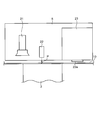
- FIG. 1 is a plan view showing a film thickness measuring apparatus according to an embodiment of the present invention.
- FIG. 2 is a side view seen from the direction of arrow U in FIG.
- the film thickness measuring apparatus includes a base 1, a substrate stage 2, a calibration stage 3, a gantry 4, a slider 5, and a plurality of measuring devices 21, 22, and 23. And control means 30.
- the substrate stage 2 includes a stage provided on the base 1 and divided into a plurality of stages. On the substrate stage 2, the formed product substrate 10 is placed.
- the substrate stage 2 is provided with a plurality of air holes 2a. By sucking air from the air holes 2a, the product substrate 10 can be brought into close contact with the substrate stage 2, while air is blown out from the air holes 2a. The product substrate 10 can be lifted from the substrate stage 2.
- the product substrate 10 is, for example, a liquid crystal TFT used for a liquid crystal display.
- the product substrate 10 includes a substrate and one or more films formed on the substrate.
- the film is formed on the substrate by, for example, a sputtering method, a vapor deposition method, or a plating method.
- the substrate is, for example, a glass substrate, and the film is a metal film such as aluminum, titanium, tungsten, or molybdenum.
- the calibration stage 3 is provided on the base 1 and is provided separately from the substrate stage 2.
- the calibration stage 3 is provided with a plurality of recesses 3a, and various types of calibration samples 60 and 70 are fitted into the recesses 3a, and the calibration samples 60 and 70 are used for the measurement devices 21, 22, and 23. Calibration is performed.
- the gantry 4 extends in the first direction with respect to the substrate stage 2 and the calibration stage 3.
- the gantry 4 is attached to the base 1 so as to be movable in the second direction with respect to the substrate stage 2 and the calibration stage 3.
- the first direction refers to the direction of arrow A
- the second direction refers to the direction of arrow B.
- the first direction and the second direction are orthogonal to each other.
- the base 1 is provided with two rail portions 6 and 6 extending in the second direction (arrow B direction).
- the two rail portions 6 and 6 are arranged so as to sandwich the substrate stage 2 and the calibration stage 3.
- the gandries 4 are stretched over the two rail portions 6 and 6 and can move along the rail portions 6 and 6 in the second direction.
- the slider 5 is attached to the gantry 4 so as to be movable in the first direction (arrow A direction).
- a camera 21, a displacement sensor 22, and a measurement head 23 as the measurement device are fixed to the slider 5.
- the measuring devices 21, 22, and 23 can cover the entire range of the substrate stage 2 and the calibration stage 3 in the second direction (arrow B direction) by the movable range Z 1 of the gun dolly 4. Further, the measuring devices 21, 22, and 23 can cover the entire range of the substrate stage 2 and the calibration stage 3 in the first direction (arrow A direction) by the movable range Z ⁇ b> 2 of the slider 5.
- the control unit 30 includes a substrate position correcting unit 31, a head position adjusting unit 32, an analyzing unit 33, and a measuring device calibration unit 34.
- the camera 21 detects the alignment mark of the product substrate 10 placed on the substrate stage 2.
- This alignment mark is a mark that can be identified by the camera 21, and is provided at, for example, the four corners of the product substrate 10.
- the substrate position correcting means 31 corrects the position information in the plane direction (first and second directions) of the product substrate 10 placed on the substrate stage 2 based on the detection result of the camera 21.
- the base 1 is provided with a plurality of clamps 7 so as to press each side around the product substrate 10. After fixing the product substrate 10 to a predetermined position by the clamp 7, the alignment mark is detected by the camera 21, and the position information of the product substrate 10 is corrected by the substrate position correcting means 31 based on the detection result.
- the displacement sensor 22 measures the distance in the height direction from the product substrate 10 placed on the substrate stage 2 as shown in FIG.
- the displacement sensor 22 irradiates a predetermined measurement point P of the product substrate 10 with light rays such as infrared rays, detects the reflected light from the measurement point P, and measures the distance to the measurement point P.
- the head position adjusting means 32 is configured so that the distance between the product substrate 10 placed on the substrate stage and the measurement head 23 becomes a predetermined constant value.
- the position of the measuring head 23 in the height direction is adjusted. Specifically, the distance in the height direction between the measurement point P of the product substrate 10 and the light emitting / receiving unit 23a of the measurement head 23 is adjusted to be 2 mm ⁇ 30 ⁇ m.
- the head position adjusting means 32 moves the measuring head 23 to a position where the measuring head 23 can measure the measurement point P of the product substrate 10 after adjusting the position of the measuring head 23 in the height direction.
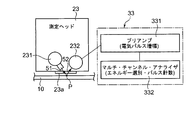
- the measurement head 23 includes an X-ray irradiation unit 231 and a fluorescent X-ray detection unit 232 as shown in FIG.
- the X-ray irradiation unit 231 irradiates the measurement point P of the product substrate 10 with the primary X-ray 51 from the light emitting / receiving unit 23a.
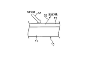
- the primary X-ray 51 is, for example, rhodium, molybdenum, tungsten, or the like. Then, as shown in FIG. 5, the film 12 on the substrate 11 of the product substrate 10 generates fluorescent X-rays 52 by irradiation with the primary X-rays 51.
- the fluorescent X-ray detector 232 detects the fluorescent X-rays 52 generated from the film 12 from the light emitting / receiving unit 23a.
- the fluorescent X-ray detector 232 is, for example, a silicon drift detector.
- the analyzing means 33 obtains the thickness of the film 12 from the intensity of the fluorescent X-ray 52 detected by the measuring head 23.
- the analysis means 33 includes a preamplifier 331 and a multi-channel analyzer (hereinafter referred to as MCA) 332.
- the preamplifier 331 amplifies the electric signal output from the fluorescent X-ray detection unit 232.
- the MCA 332 analyzes the electrical signal amplified by the preamplifier 331. In the MCA 332, the energy output from the fluorescent X-ray detection unit 232 is selected, and the pulse is measured to obtain the X-ray intensity of the elements constituting the film 12. And based on this X-ray intensity, the thickness of the film
- the film 12 is a titanium film or a molybdenum film
- the relationship between the X-ray intensity and the film thickness is as shown in FIGS. 6A and 6B.
- the measurement of the thickness of the single-layer film has been described, but the thickness of the multiple-layer film can also be measured.
- fluorescent X-rays generated from each film are detected by the measuring head 23, and the X-ray intensity of each element constituting each film is obtained by the analyzing means 33, and the thickness of each film is determined based on this X-ray intensity.
- the composition ratio of each element can also be obtained from the X-ray intensity of each element.
- the measuring device calibration means 34 moves the measuring devices 21, 22, and 23 to the calibration stage 3 to calibrate the measuring devices 21, 22, and 23. Calibration of the measuring devices 21, 22, and 23 is performed at predetermined intervals.
- the predetermined interval is, for example, every predetermined time such as performing calibration once a day, or every predetermined number of processes such as performing calibration after measuring the film thickness of a predetermined number of product substrates 10.
- a gain calibration sample 60 and an offset amount calibration sample 70 are installed in the calibration stage 3.
- the gain calibration sample 60 is a sample for adjusting the gain of the fluorescent X-ray detection unit 232 of the measurement head 23.
- the offset amount calibration sample 70 is a sample for adjusting the offset amount of each measuring device 21, 22, 23.
- the offset amount calibration sample 70 includes a first offset amount detector 71 and a second offset amount detector 72 as shown in FIG.
- the first offset amount detection unit 71 is a part for obtaining the positional relationship between the camera 21 and the measurement head 23.
- the second offset amount detection unit 72 is a part for obtaining the positional relationship between the camera 21 and the displacement sensor 22.
- the first offset amount detection unit 71 includes a first portion 711 and a second portion 712 adjacent to the first portion 711.
- the first and second portions 711 and 712 are indicated by hatching.
- the first part 711 is made of a first substance.
- the second portion 712 is made of a second material different from the first material.
- the first material is copper
- the second material is titanium.
- the area of the first portion 711 is larger than the area of the second portion 712.
- the boundary between the first portion 711 and the second portion 712 includes an X-axis boundary line Lx along the X-axis direction and a Y-axis boundary line Ly along the Y-axis direction.
- Marks 713 that can be recognized by the camera 21 are provided on the X-axis boundary line Lx and the Y-axis boundary line Ly, respectively.
- the X-axis direction is the left-to-right direction in FIG. 1 (that is, the arrow B direction)
- the Y-axis direction is the top-to-down direction (that is, the arrow A direction) in FIG.
- the second offset amount detection unit 72 includes a through hole 720.
- the through hole 720 is provided in the first portion 711.
- the inner surface of the through-hole 720 is formed in a rectangular shape, and the rectangle includes two sides along the X-axis direction and two sides along the Y-axis direction.
- the inner surface of the through hole 720 is, for example, a square having a side of 4 mm.
- a mark 713 on the Y-axis boundary line Ly is detected from the image G1 of the camera 21, and the X coordinate of the camera 21 is calculated.
- the primary X-ray beam B1 from the measurement head 23 is scanned in the X-axis direction, the Y-axis boundary line Ly is detected with this beam B1, and the X coordinate of the measurement head 23 is calculated.
- the Y-axis boundary line Ly is derived from the difference between the fluorescent X-rays generated from the first material of the first portion 711 and the fluorescent X-rays generated from the second material of the second portion 712. Can be detected.
- the mark 713 on the X-axis boundary line Lx is detected from the image G2 of the camera 21, and the Y coordinate of the camera 21 is calculated.
- the primary X-ray beam B2 from the measurement head 23 is scanned in the Y-axis direction, and the X-axis boundary line Lx is detected by this beam B2, and the Y coordinate of the measurement head 23 is calculated.
- an offset amount ( ⁇ X, ⁇ Y) between the camera 21 and the measurement head 23 is obtained from the X coordinate of the camera 21 and the measurement head 23 and the Y coordinate of the camera 21 and the measurement head 23.
- the center point 720a of the through hole 720 is detected from the image G1 of the camera 21, and the X coordinate and Y coordinate of the camera 21 are calculated.
- the beam B1 of the light beam from the displacement sensor 22 is scanned in the X-axis direction, the center point 720a of the through-hole 720 is detected with this beam B1, and the X coordinate of the displacement sensor 22 is calculated. Since the reflected light of the displacement sensor 22 is not detected in the through hole 720, the through hole 720 can be specified by the displacement sensor 22.
- the beam B2 of the light beam from the displacement sensor 22 is scanned in the Y-axis direction, the center point 720a of the through-hole 720 is detected with this beam B2, and the Y coordinate of the displacement sensor 22 is calculated.
- an offset amount ( ⁇ X, ⁇ Y) between the camera 21 and the displacement sensor 22 is obtained from the X coordinate of the camera 21 and the displacement sensor 22 and the Y coordinate of the camera 21 and the displacement sensor 22.
- the position of the camera 21, the displacement sensor 22 and the measurement head 23 can be determined.
- the change is checked, and the alignment of the camera 21, the displacement sensor 22, and the measuring head 23 is adjusted by a program.
- the product substrate 10 is transferred onto the substrate stage 2 from the right direction (arrow R direction) of the film thickness measuring apparatus.
- the product substrate 10 transported onto the substrate stage 2 is fixed at a predetermined position by the clamp 7.
- the alignment mark is detected by the camera 21, and the position information of the product substrate 10 is corrected by the substrate position correcting unit 31 based on the detection result.
- the head position adjusting means 32 adjusts the position of the measuring head 23 in the height direction so that the distance between the first measuring point and the measuring head 23 becomes a constant value based on this measured value. To do.
- the measurement head 23 is moved directly above the first measurement point by the head position adjusting means 32, and the film of the product substrate 10 is irradiated with primary X-rays to detect fluorescent X-rays generated from this film. To do. Then, the analysis means 33 obtains the thickness of the film from the detected intensity of the fluorescent X-ray.
- the film thickness of the other measurement points is measured by the measurement head 23.
- the film thicknesses of all the measurement points of the product substrate 10 are measured, and it is determined whether or not the product substrate 10 is defective based on the measurement result.
- the measuring instrument calibration means 34 moves the measuring instruments 21, 22, 23 to the calibration stage 3 at predetermined intervals, and calibrates the measuring instruments 21, 22, 23 using the calibration samples 60, 70. .
- the offset amount calibration sample 70 having the above configuration, since the first offset amount detection unit 71 and the second offset amount detection unit 72 are provided, three different types of cameras 21 and displacement sensors are used in one calibration sample.
- the positional relationship between 22 and the measurement head 23 can be obtained. That is, the positions of the displacement sensor 22 and the measurement head 23 can be calibrated with the camera 21 as a reference.
- the position of the two types of displacement sensors 22 and the measurement head 23 can be calibrated with one calibration sample, and the labor for calibration of the film thickness measuring apparatus can be saved.
- the first offset amount detection unit 71 includes a first portion 711 made of a first material and a second portion 712 made of a second material different from the first material and adjacent to the first portion 711. Is done. Thereby, the positional relationship (offset amount) between the camera 21 and the measurement head 23 can be obtained from the position coordinates of the camera 21 and the position coordinates of the measurement head 23. Therefore, the position of the measuring head 23 can be calibrated with a simple configuration.
- a mark 713 that can be recognized by the camera 21 is provided at the boundary between the first portion 711 and the second portion 712. As a result, the camera 21 can accurately detect the boundary between the first portion 711 and the second portion 712 and accurately determine the position coordinates of the camera 21.
- the second offset amount detection unit 72 includes a through hole 720. Accordingly, the positional relationship (offset amount) between the camera 21 and the displacement sensor 22 can be obtained from the position coordinates of the camera 21 and the position coordinates of the displacement sensor 22. Therefore, the position of the displacement sensor 22 can be calibrated with a simple configuration.
- the measuring instrument calibration unit 34 uses the offset amount calibration sample 70 to determine the positional relationship between the camera 21 and the measurement head 23, and the camera 21. The positional relationship with the displacement sensor 22 is obtained. Thereby, the position of the two types of displacement sensor 22 and the measurement head 23 can be calibrated with one offset amount calibration sample 70, and the labor of calibration of the film thickness measuring apparatus can be saved.
- the film thickness is obtained by the fluorescent X-ray analysis method, it is possible to measure a minute region of the film 12 of the product substrate 10 and improve the film thickness measurement accuracy. Further, in the fluorescent X-ray analysis method, the film thickness measurement time can be shortened as compared with the X-ray reflectance method.
- the measurement head 23 is movable in the first direction and the second direction with respect to the substrate stage 2, the film thickness at a plurality of locations on the product substrate 10 can be measured with the measurement head 23. Thereby, it becomes suitable for the film thickness measurement of the large-sized product substrate 10.
- the present invention is not limited to the above-described embodiment.
- the camera 21 can recognize the boundary between the first portion 711 and the second portion 712 of the offset amount calibration sample 70, the mark 713 may not be provided at this boundary.
- the second offset amount detection unit 72 of the offset amount calibration sample 70 may be a substance that does not reflect the light beam of the displacement sensor 22 instead of the through hole 720.
- first direction that is the extending direction of the gantry 4 and the second direction that is the moving direction of the gantry 4 may cross each other without being orthogonal to each other.
- the number of the camera 21, the displacement sensor 22, and the measuring head 23 is not limited to one, and may be plural.
- calibration samples 60 and 70 are installed on the calibration stage 3, the number of calibration samples can be freely increased or decreased. Also, other types of calibration samples may be used, for example, calibration samples for calibrating X-ray intensity drift.
- the film thickness measuring device of the present invention may be used to measure the film thickness of a small product substrate.
- the film thickness of a semiconductor substrate such as an organic EL may be measured. Also good.
Landscapes
- Physics & Mathematics (AREA)
- General Physics & Mathematics (AREA)
- Electromagnetism (AREA)
- Length-Measuring Devices Using Wave Or Particle Radiation (AREA)
- Length Measuring Devices By Optical Means (AREA)
- Length Measuring Devices With Unspecified Measuring Means (AREA)
Abstract
オフセット量校正試料(70)は、第1オフセット量検出部(71)と第2オフセット量検出部(72)とを備える。第1オフセット量検出部(71)は、カメラ(21)と測定ヘッド(23)との位置関係を求めるための部分である。第2オフセット量検出部(72)は、カメラ(21)と変位センサ(22)との位置関係を求めるための部分である。
Description
この発明は、オフセット量校正試料および膜厚測定装置に関する。
従来、膜厚測定装置に用いられるオフセット量校正試料としては、特開2010-210389号公報(特許文献1)に記載されたものがある。この校正試料の複数の位置で撮像し、各位置でのスポット光に基づいて校正試料の膜厚をそれぞれ計測する。そして、撮像した画像を処理して、画像の中心と校正試料の中心との中心位置の差を算出し、この中心位置の差に対する膜厚の変化に基づいて、画像の中心に対するスポット光のずれ量を求める。
ところで、上記従来のオフセット量校正試料では、撮像画像内のスポット光のずれ量を求めることができるが、上記膜厚測定装置の他の測定機器の位置の校正を行おうとすると、別の校正試料を用意しなければならず、面倒であった。
そこで、この発明の課題は、2種類の測定機器の位置の校正を行うことができて、校正の作業の手間を省くことができるオフセット量校正試料および膜厚測定装置を提供することにある。
上記課題を解決するため、この発明のオフセット量校正試料は、
成膜された製品基板の位置情報を補正するためのカメラと、上記製品基板との距離を調整するための変位センサと、上記製品基板の膜の厚みを測定するための測定ヘッドとを有する膜厚測定装置の校正に用いられる校正試料であって、
上記カメラと上記測定ヘッドとの位置関係を求めるための第1オフセット量検出部と、
上記カメラと上記変位センサとの位置関係を求めるための第2オフセット量検出部と
を備えることを特徴としている。
成膜された製品基板の位置情報を補正するためのカメラと、上記製品基板との距離を調整するための変位センサと、上記製品基板の膜の厚みを測定するための測定ヘッドとを有する膜厚測定装置の校正に用いられる校正試料であって、
上記カメラと上記測定ヘッドとの位置関係を求めるための第1オフセット量検出部と、
上記カメラと上記変位センサとの位置関係を求めるための第2オフセット量検出部と
を備えることを特徴としている。
ここで、上記製品基板は、基板と、この基板上に形成された一層以上の膜とを有する。
この発明のオフセット量校正試料によれば、上記第1オフセット量検出部と上記第2オフセット量検出部とを備えるので、1つの校正試料において、種類の異なる3つのカメラ、変位センサおよび測定ヘッドの位置関係を求めることができる。つまり、カメラを基準として、変位センサと測定ヘッドの位置の校正を行うことができる。
したがって、1つの校正試料で、2種類の変位センサおよび測定ヘッドの位置の校正を行うことができ、膜厚測定装置の校正の作業の手間を省くことができる。
また、一実施形態のオフセット量校正試料では、
上記測定ヘッドは、上記製品基板の上記膜に1次X線を照射してこの膜から発生する蛍光X線を検出するように、構成され、
上記第1オフセット量検出部は、
第1物質からなる第1部分と、
上記第1物質と異なる第2物質からなると共に、上記第1部分に隣接する第2部分と
から構成される。
上記測定ヘッドは、上記製品基板の上記膜に1次X線を照射してこの膜から発生する蛍光X線を検出するように、構成され、
上記第1オフセット量検出部は、
第1物質からなる第1部分と、
上記第1物質と異なる第2物質からなると共に、上記第1部分に隣接する第2部分と
から構成される。
この実施形態のオフセット量校正試料によれば、上記第1オフセット量検出部は、第1物質からなる第1部分と、上記第1物質と異なる第2物質からなると共に上記第1部分に隣接する第2部分とから構成される。
そして、上記カメラで、上記第1部分と上記第2部分との境界を、画像により検出して、カメラの位置座標を求める。上記測定ヘッドで、上記第1部分と上記第2部分との境界を、上記第1物質から発生する蛍光X線と上記第2物質から発生する蛍光X線とに基づいて、検出して、測定ヘッドの位置座標を求める。
これにより、上記カメラの位置座標と上記測定ヘッドの位置座標とから、カメラと測定ヘッドとの位置関係(オフセット量)を求めることができる。したがって、簡単な構成で、測定ヘッドの位置の校正を行うことができる。
また、一実施形態のオフセット量校正試料では、上記第1部分と上記第2部分との境界に、上記カメラで認識可能なマークが設けられている。
この実施形態のオフセット量校正試料によれば、上記第1部分と上記第2部分との境界に、上記カメラで認識可能なマークが設けられている。これにより、カメラで、第1部分と第2部分との境界を正確に検出して、カメラの位置座標を正確に求めることができる。
また、一実施形態のオフセット量校正試料では、
上記変位センサは、上記製品基板に光線を照射してこの製品基板からの反射光を検出するように、構成され、
上記第2オフセット量検出部は、貫通孔から構成される。
上記変位センサは、上記製品基板に光線を照射してこの製品基板からの反射光を検出するように、構成され、
上記第2オフセット量検出部は、貫通孔から構成される。
この実施形態のオフセット量校正試料によれば、上記第2オフセット量検出部は、貫通孔から構成される。
そして、上記カメラで、上記貫通孔を、画像により検出して、カメラの位置座標を求める。上記貫通孔では、上記変位センサの反射光が検出されないことから、変位センサで、貫通孔を特定して、変位センサの位置座標を求める。
これにより、上記カメラの位置座標と上記変位センサの位置座標とから、カメラと変位センサとの位置関係(オフセット量)を求めることができる。したがって、簡単な構成で、変位センサの位置の校正を行うことができる。
また、一実施形態の膜厚測定装置では、
基台と、
上記基台に設けられると共に、成膜された製品基板を載置する基板ステージと、
上記基台に設けられると共に、請求項1から4の何れか一つに記載の上記オフセット量校正試料を載置する校正ステージと、
上記基板ステージおよび上記校正ステージに対して第1方向に延在すると共に、上記基板ステージおよび上記校正ステージに対して第2方向に移動可能となるように上記基台に取り付けられるガントリーと、
上記ガントリーに上記第1方向に移動可能に取り付けられるスライダーと、
上記スライダーに固定されると共に、上記基板ステージに載置された上記製品基板の位置情報を補正するためのカメラと、
上記スライダーに固定されると共に、上記基板ステージに載置された上記製品基板との距離を調整するための変位センサと、
上記スライダーに固定されると共に、上記基板ステージに載置された上記製品基板の膜の厚みを測定するための測定ヘッドと、
上記測定ヘッド、上記カメラおよび上記変位センサを上記校正ステージに移動し、上記校正ステージに載置された上記オフセット量校正試料を用いて、上記カメラと上記測定ヘッドとの位置関係、および、上記カメラと上記変位センサとの位置関係を求める測定機器校正手段と
を備える。
基台と、
上記基台に設けられると共に、成膜された製品基板を載置する基板ステージと、
上記基台に設けられると共に、請求項1から4の何れか一つに記載の上記オフセット量校正試料を載置する校正ステージと、
上記基板ステージおよび上記校正ステージに対して第1方向に延在すると共に、上記基板ステージおよび上記校正ステージに対して第2方向に移動可能となるように上記基台に取り付けられるガントリーと、
上記ガントリーに上記第1方向に移動可能に取り付けられるスライダーと、
上記スライダーに固定されると共に、上記基板ステージに載置された上記製品基板の位置情報を補正するためのカメラと、
上記スライダーに固定されると共に、上記基板ステージに載置された上記製品基板との距離を調整するための変位センサと、
上記スライダーに固定されると共に、上記基板ステージに載置された上記製品基板の膜の厚みを測定するための測定ヘッドと、
上記測定ヘッド、上記カメラおよび上記変位センサを上記校正ステージに移動し、上記校正ステージに載置された上記オフセット量校正試料を用いて、上記カメラと上記測定ヘッドとの位置関係、および、上記カメラと上記変位センサとの位置関係を求める測定機器校正手段と
を備える。
ここで、上記製品基板は、基板と、この基板上に形成された一層以上の膜とを有する。
この実施形態の膜厚測定装置によれば、上記測定機器校正手段は、上記オフセット量校正試料を用いて、上記カメラと上記測定ヘッドとの位置関係、および、上記カメラと上記変位センサとの位置関係を求める。
これにより、1つのオフセット量校正試料で、2種類の変位センサおよび測定ヘッドの位置の校正を行うことができ、膜厚測定装置の校正の作業の手間を省くことができる。
この発明のオフセット量校正試料によれば、上記第1オフセット量検出部と上記第2オフセット量検出部とを備えるので、2種類の測定機器の位置の校正を行うことができて、校正の作業の手間を省くことができる。
この発明の膜厚測定装置によれば、上記測定機器校正手段は、上記オフセット量校正試料を用いて、上記カメラと上記測定ヘッドとの位置関係、および、上記カメラと上記変位センサとの位置関係を求める。これにより、1つのオフセット量校正試料で、2種類の変位センサおよび測定ヘッドの位置の校正を行うことができ、膜厚測定装置の校正の作業の手間を省くことができる。
以下、この発明を図示の実施の形態により詳細に説明する。
図1は、この発明の一実施形態の膜厚測定装置を示す平面図である。図2は、図1の矢印U方向からみた側面図である。図1と図2に示すように、この膜厚測定装置は、基台1と、基板ステージ2と、校正ステージ3と、ガンドリー4と、スライダー5と、複数の測定機器21,22,23と、制御手段30とを有する。
上記基板ステージ2は、上記基台1に設けられ、複数に分割されたステージからなる。基板ステージ2上には、成膜された製品基板10が載置される。
上記基板ステージ2には、複数の空気孔2aが設けられ、この空気孔2aからエアを吸い込むことで、製品基板10を基板ステージ2に密着でき、一方、空気孔2aからエアを吹き出すことで、製品基板10を基板ステージ2から浮上できる。
上記製品基板10は、例えば、液晶ディスプレイに用いられる液晶TFTである。この製品基板10は、基板と、この基板上に形成された一層以上の膜とを有する。上記膜は、例えば、スパッタリング工法や蒸着工法やメッキ工法により、上記基板に成膜される。上記基板は、例えば、ガラス基板であり、上記膜は、例えば、アルミニウム、チタン、タングステン、モリブデンなどの金属膜である。
上記校正ステージ3は、上記基台1に設けられ、上記基板ステージ2とは別に設けられる。この校正ステージ3には、複数の凹部3aが設けられ、この凹部3aに様々な種類の校正試料60,70が嵌め込まれ、この校正試料60,70を用いて上記測定機器21,22,23の校正が行われる。
上記ガントリー4は、上記基板ステージ2および上記校正ステージ3に対して第1方向に延在する。ガンドリー4は、基板ステージ2および校正ステージ3に対して第2方向に移動可能となるように、基台1に取り付けられる。第1方向とは、矢印A方向をいい、第2方向とは、矢印B方向をいう。第1方向と第2方向とは、互いに直交する。
つまり、上記基台1には、第2方向(矢印B方向)に延在する2本のレール部6,6が設けられている。この2本のレール部6,6は、基板ステージ2および校正ステージ3を挟むように、配置されている。上記ガンドリー4は、この2本のレール部6,6に架け渡され、このレール部6,6に沿って第2方向に移動可能となる。
上記スライダー5は、上記ガントリー4に第1方向(矢印A方向)に移動可能に取り付けられる。このスライダー5には、上記測定機器としてのカメラ21、変位センサ22および測定ヘッド23が、固定されている。
そして、上記測定機器21,22,23は、ガンドリー4の可動範囲Z1により、基板ステージ2および校正ステージ3の第2方向(矢印B方向)の全範囲をカバーできる。また、上記測定機器21,22,23は、スライダー5の可動範囲Z2により、基板ステージ2および校正ステージ3の第1方向(矢印A方向)の全範囲をカバーできる。
上記制御手段30は、基板位置補正手段31と、ヘッド位置調整手段32と、解析手段33と、測定機器校正手段34とを有する。
上記カメラ21は、基板ステージ2に載置された製品基板10のアライメントマークを検出する。このアライメントマークは、カメラ21で判別可能なマークであり、例えば、製品基板10の四隅に設けられる。
上記基板位置補正手段31は、上記カメラ21の検出結果に基づいて、基板ステージ2に載置された製品基板10の平面方向(第1、第2方向)の位置情報を補正する。具体的に述べると、上記基台1には、製品基板10の周囲の各辺を押圧するように、複数のクランプ7が設けられている。クランプ7により製品基板10を所定の位置に固定後、カメラ21にてアライメントマークを検出し、この検出結果に基づいて基板位置補正手段31によって、製品基板10の位置情報を補正する。
上記変位センサ22は、図3に示すように、基板ステージ2に載置された製品基板10との高さ方向の距離を測定する。変位センサ22は、例えば赤外線などの光線を、製品基板10の予め定めた測定ポイントPに照射し、この測定ポイントPからの反射光を検出して、測定ポイントPとの距離を測定する。
上記ヘッド位置調整手段32は、上記変位センサ22の測定値に基づいて、基板ステージに載置された製品基板10と測定ヘッド23との間の距離が予め定められた一定値となるように、測定ヘッド23の高さ方向の位置を調整する。具体的に述べると、製品基板10の測定ポイントPと測定ヘッド23の受発光部23aとの間の高さ方向の距離が、2mm±30μmとなるように、調整される。
また、上記ヘッド位置調整手段32は、測定ヘッド23の高さ方向の位置を調整した後、測定ヘッド23が製品基板10の測定ポイントPを測定できる位置に、測定ヘッド23を移動する。
上記測定ヘッド23は、図4に示すように、X線照射部231と蛍光X線検出部232とを有する。
上記X線照射部231は、受発光部23aから製品基板10の測定ポイントPへ、1次X線51を照射する。1次X線51は、例えば、ロジウムや、モリブデンや、タングステンなどである。すると、図5に示すように、製品基板10の基板11上の膜12は、1次X線51の照射により、蛍光X線52を発生する。
上記蛍光X線検出部232は、上記膜12から発生した上記蛍光X線52を、受発光部23aから検出する。蛍光X線検出部232は、例えば、シリコンドリフト検出器である。
上記解析手段33は、上記測定ヘッド23により検出された上記蛍光X線52の強度から上記膜12の厚みを求める。具体的に述べると、解析手段33は、プリアンプ331とマルチ・チャンネル・アナライザ(以下、MCAという)332とを有する。
上記プリアンプ331は、蛍光X線検出部232から出力される電気信号を増幅する。上記MCA332は、プリアンプ331で増幅された電気信号を解析する。MCA332では、蛍光X線検出部232から出力されたエネルギーを選別し、パルスを計測することで、膜12を構成する元素のX線強度を求める。そして、このX線強度に基づいて、既知のデータから、膜12の厚みを求める。なお、MCA332を用いているため、膜12に混入する異物や不純物を検出できる。
例えば、上記膜12が、チタン膜、または、モリブデン膜である場合、X線強度と膜厚との関係は、図6Aと図6Bに示すような関係となる。
なお、上述では、単層の膜(図5)の厚みの測定を説明したが、複数層の膜の厚みを測定することもできる。この場合、各膜から発生する蛍光X線を測定ヘッド23によって検出し、解析手段33によって、各膜を構成する各元素のX線強度を求め、このX線強度に基づいて、各膜の厚みを求める。さらに、この各元素のX線強度から、各元素の組成比をも、求めることができる。
上記測定機器校正手段34は、図1に示すように、上記測定機器21,22,23を校正ステージ3に移動して、測定機器21,22,23の校正を行う。測定機器21,22,23の校正は、所定間隔で、行う。この所定間隔とは、例えば、1日に1回の校正を行うといった所定時間毎や、所定枚数の製品基板10の膜厚を測定した後に校正を行うといった所定処理数毎である。
上記校正ステージ3には、ゲイン校正試料60とオフセット量校正試料70とが、設置されている。ゲイン校正試料60は、測定ヘッド23の蛍光X線検出部232のゲインを調整するための試料である。オフセット量校正試料70は、各測定機器21,22,23のオフセット量を調整するための試料である。
上記オフセット量校正試料70は、図7に示すように、第1オフセット量検出部71と第2オフセット量検出部72とを備える。上記第1オフセット量検出部71は、上記カメラ21と上記測定ヘッド23との位置関係を求めるための部分である。上記第2オフセット量検出部72は、上記カメラ21と上記変位センサ22との位置関係を求めるための部分である。
上記第1オフセット量検出部71は、第1部分711と、この第1部分711に隣接する第2部分712とから構成される。上記第1、上記第2部分711,712を、それぞれ、ハッチングにて示す。
上記第1部分711は、第1物質からなる。上記第2部分712は、上記第1物質と異なる第2物質からなる。例えば、上記第1物質は、銅であり、上記第2物質は、チタンである。第1部分711の面積は、第2部分712の面積よりも、大きい。
上記第1部分711と上記第2部分712との間の境界には、X軸方向に沿ったX軸境界線Lxと、Y軸方向に沿ったY軸境界線Lyとを含む。X軸境界線LxおよびY軸境界線Lyには、それぞれ、上記カメラ21で認識可能なマーク713が設けられている。なお、X軸方向とは、図1の左から右方向(つまり、矢印B方向)であり、Y軸方向とは、図1の上から下方向(つまり、矢印A方向)である。
上記第2オフセット量検出部72は、貫通孔720から構成される。この貫通孔720は、上記第1部分711に設けられている。貫通孔720の内面は、矩形状に形成され、この矩形は、X軸方向に沿った2つの辺とY軸方向に沿った2つの辺とからなる。貫通孔720の内面は、例えば、1辺4mmの正方形である。
上記オフセット量校正試料70を用いて、上記カメラ21と上記測定ヘッド23との位置関係を求める方法を説明する。
図8に示すように、まず、上記カメラ21の画像G1で、Y軸境界線Ly上のマーク713を検出して、カメラ21のX座標を算出する。
そして、上記測定ヘッド23からの1次X線のビームB1をX軸方向に走査させ、このビームB1でY軸境界線Lyを検出して、測定ヘッド23のX座標を算出する。この測定ヘッド23では、上記第1部分711の上記第1物質から発生する蛍光X線と、上記第2部分712の上記第2物質から発生する蛍光X線との違いから、Y軸境界線Lyを検出することができる。
その後、上記カメラ21の画像G2で、X軸境界線Lx上のマーク713を検出して、カメラ21のY座標を算出する。そして、上記測定ヘッド23からの1次X線のビームB2をY軸方向に走査させ、このビームB2でX軸境界線Lxを検出して、測定ヘッド23のY座標を算出する。
その後、上記カメラ21および上記測定ヘッド23のX座標と、上記カメラ21および上記測定ヘッド23のY座標とから、カメラ21と測定ヘッド23のオフセット量(ΔX、ΔY)を求める。
上記オフセット量校正試料70を用いて、上記カメラ21と上記変位センサ22との位置関係を求める方法を説明する。
図9に示すように、まず、上記カメラ21の画像G1で、貫通孔720の中心点720aを検出して、カメラ21のX座標およびY座標を算出する。
そして、上記変位センサ22からの光線のビームB1をX軸方向に走査させ、このビームB1で貫通孔720の中心点720aを検出して、変位センサ22のX座標を算出する。この貫通孔720では、変位センサ22の反射光が検出されないことから、変位センサ22で、貫通孔720を特定することができる。
その後、上記変位センサ22からの光線のビームB2をY軸方向に走査させ、このビームB2で貫通孔720の中心点720aを検出して、変位センサ22のY座標を算出する。
その後、上記カメラ21および上記変位センサ22のX座標と、上記カメラ21および上記変位センサ22のY座標とから、カメラ21と変位センサ22のオフセット量(ΔX、ΔY)を求める。
このようにして、上記カメラ21と上記測定ヘッド23との位置関係、および、上記カメラ21と上記変位センサ22との位置関係を求めることで、カメラ21、変位センサ22および測定ヘッド23の位置の変化をチェックしたり、カメラ21、変位センサ22および測定ヘッド23の位置合わせをプログラムで調整する。
次に、上記構成の膜厚測定装置の動作を説明する。
図1に示すように、まず、上記製品基板10が、膜厚測定装置の右方向(矢印R方向)から基板ステージ2上に、搬送される。基板ステージ2上に搬送された製品基板10は、クランプ7により所定の位置に固定される。その後、カメラ21にてアライメントマークを検出し、この検出結果に基づいて基板位置補正手段31によって、製品基板10の位置情報を補正する。
その後、上記製品基板10の複数の測定ポイントのうちの第1の測定ポイントにおいて、変位センサ22により、第1の測定ポイントと変位センサ22との間の高さ方向の距離を測定する。そして、上記ヘッド位置調整手段32は、この測定値に基づいて、第1の測定ポイントと測定ヘッド23との間の距離が一定値となるように、測定ヘッド23の高さ方向の位置を調整する。
その後、上記測定ヘッド23は、ヘッド位置調整手段32により、第1の測定ポイントの直上に移動され、製品基板10の膜に1次X線を照射してこの膜から発生する蛍光X線を検出する。そして、上記解析手段33は、この検出された蛍光X線の強度から膜の厚みを求める。
その後、上記製品基板10の他の測定ポイントについても、同様に、測定ヘッド23の高さを調整してから、測定ヘッド23によって他の測定ポイントの膜厚を測定する。
このようにして、上記製品基板10の全ての測定ポイントの膜厚を測定し、この測定結果に基づいて、製品基板10が不良品であるか否かを判断する。
その後、上記測定機器校正手段34は、所定間隔で、上記測定機器21,22,23を校正ステージ3に移動して、校正試料60,70を用いて測定機器21,22,23の校正を行う。
上記構成のオフセット量校正試料70によれば、上記第1オフセット量検出部71と上記第2オフセット量検出部72とを備えるので、1つの校正試料において、種類の異なる3つのカメラ21、変位センサ22および測定ヘッド23の位置関係を求めることができる。つまり、カメラ21を基準として、変位センサ22と測定ヘッド23の位置の校正を行うことができる。
したがって、1つの校正試料で、2種類の変位センサ22および測定ヘッド23の位置の校正を行うことができ、膜厚測定装置の校正の作業の手間を省くことができる。
また、上記第1オフセット量検出部71は、第1物質からなる第1部分711と、上記第1物質と異なる第2物質からなると共に上記第1部分711に隣接する第2部分712とから構成される。これにより、上記カメラ21の位置座標と上記測定ヘッド23の位置座標とから、カメラ21と測定ヘッド23との位置関係(オフセット量)を求めることができる。したがって、簡単な構成で、測定ヘッド23の位置の校正を行うことができる。
また、上記第1部分711と上記第2部分712との境界に、上記カメラ21で認識可能なマーク713が設けられている。これにより、カメラ21で、第1部分711と第2部分712との境界を正確に検出して、カメラ21の位置座標を正確に求めることができる。
また、上記第2オフセット量検出部72は、貫通孔720から構成される。これにより、上記カメラ21の位置座標と上記変位センサ22の位置座標とから、カメラ21と変位センサ22との位置関係(オフセット量)を求めることができる。したがって、簡単な構成で、変位センサ22の位置の校正を行うことができる。
また、上記構成の膜厚測定装置によれば、上記測定機器校正手段34は、上記オフセット量校正試料70を用いて、上記カメラ21と上記測定ヘッド23との位置関係、および、上記カメラ21と上記変位センサ22との位置関係を求める。これにより、1つのオフセット量校正試料70で、2種類の変位センサ22および測定ヘッド23の位置の校正を行うことができ、膜厚測定装置の校正の作業の手間を省くことができる。
また、蛍光X線分析法により膜厚を求めるので、製品基板10の膜12の微小領域を測定できて、膜厚の測定精度を向上できる。また、蛍光X線分析法では、X線反射率法に比べて、膜厚の測定時間を短縮できる。
また、上記測定ヘッド23は、上記基板ステージ2に対して第1方向および第2方向に移動可能であるので、この測定ヘッド23で、製品基板10の複数箇所の膜厚を測定できる。これにより、大型の製品基板10の膜厚測定に好適となる。
なお、この発明は上述の実施形態に限定されない。例えば、オフセット量校正試料70の第1部分711と第2部分712との境界が、カメラ21で認識可能であれば、この境界にマーク713を設けなくてもよい。
また、オフセット量校正試料70の第2オフセット量検出部72として、貫通孔720でなく、変位センサ22の光線を反射しない物質であってもよい。
また、ガントリー4の延在方向である第1方向と、ガントリー4の移動方向である第2方向とは、互いに直交しないで、交差するようにしてもよい。
また、カメラ21、変位センサ22および測定ヘッド23の数量は、一つに限らず、複数であってもよい。
また、校正ステージ3には、2つの校正試料60,70を設置しているが、校正試料の数量の増減は、自由である。また、他の種類の校正試料であってもよく、例えば、X線強度のドリフトを校正するための校正試料であってもよい。
また、本発明の膜厚測定装置にて、小型の製品基板の膜厚を測定するようにしてもよく、また、液晶TFT以外に、有機ELなどの半導体基板の膜厚を測定するようにしてもよい。
1 基台
2 基板ステージ
3 校正ステージ
4 ガントリー
5 スライダー
6 レール部
7 クランプ
10 製品基板
21 カメラ
22 変位センサ
23 測定ヘッド
30 制御手段
31 基板位置補正手段
32 ヘッド位置調整手段
33 解析手段
34 測定機器校正手段
60 ゲイン校正試料
70 オフセット量校正試料
71 第1オフセット量検出部
711 第1部分
712 第2部分
713 マーク
72 第2オフセット量検出部
720 貫通孔
A 第1方向
B 第2方向
2 基板ステージ
3 校正ステージ
4 ガントリー
5 スライダー
6 レール部
7 クランプ
10 製品基板
21 カメラ
22 変位センサ
23 測定ヘッド
30 制御手段
31 基板位置補正手段
32 ヘッド位置調整手段
33 解析手段
34 測定機器校正手段
60 ゲイン校正試料
70 オフセット量校正試料
71 第1オフセット量検出部
711 第1部分
712 第2部分
713 マーク
72 第2オフセット量検出部
720 貫通孔
A 第1方向
B 第2方向
Claims (5)
- 成膜された製品基板(10)の位置情報を補正するためのカメラ(21)と、上記製品基板(10)との距離を調整するための変位センサ(22)と、上記製品基板(10)の膜(12)の厚みを測定するための測定ヘッド(23)とを有する膜厚測定装置の校正に用いられる校正試料であって、
上記カメラ(21)と上記測定ヘッド(23)との位置関係を求めるための第1オフセット量検出部(71)と、
上記カメラ(21)と上記変位センサ(22)との位置関係を求めるための第2オフセット量検出部(72)と
を備えることを特徴とするオフセット量校正試料。 - 請求項1に記載のオフセット量校正試料において、
上記測定ヘッド(23)は、上記製品基板(10)の上記膜(12)に1次X線を照射してこの膜(12)から発生する蛍光X線を検出するように、構成され、
上記第1オフセット量検出部(71)は、
第1物質からなる第1部分(711)と、
上記第1物質と異なる第2物質からなると共に、上記第1部分(711)に隣接する第2部分(712)と
から構成されることを特徴とするオフセット量校正試料。 - 請求項2に記載のオフセット量校正試料において、
上記第1部分(711)と上記第2部分(712)との境界に、上記カメラ(21)で認識可能なマーク(713)が設けられていることを特徴とするオフセット量校正試料。 - 請求項1から3の何れか一つに記載のオフセット量校正試料において、
上記変位センサ(22)は、上記製品基板(10)に光線を照射してこの製品基板(10)からの反射光を検出するように、構成され、
上記第2オフセット量検出部(72)は、貫通孔(720)から構成されることを特徴とするオフセット量校正試料。 - 基台(1)と、
上記基台(1)に設けられると共に、成膜された製品基板(10)を載置する基板ステージ(2)と、
上記基台(1)に設けられると共に、請求項1から4の何れか一つに記載の上記オフセット量校正試料(70)を載置する校正ステージ(3)と、
上記基板ステージ(2)および上記校正ステージ(3)に対して第1方向(A)に延在すると共に、上記基板ステージ(2)および上記校正ステージ(3)に対して第2方向(B)に移動可能となるように上記基台(1)に取り付けられるガントリー(4)と、
上記ガントリー(4)に上記第1方向(A)に移動可能に取り付けられるスライダー(5)と、
上記スライダー(5)に固定されると共に、上記基板ステージ(2)に載置された上記製品基板(10)の位置情報を補正するためのカメラ(21)と、
上記スライダー(5)に固定されると共に、上記基板ステージ(2)に載置された上記製品基板(10)との距離を調整するための変位センサ(22)と、
上記スライダー(5)に固定されると共に、上記基板ステージ(2)に載置された上記製品基板(10)の膜(12)の厚みを測定するための測定ヘッド(23)と、
上記測定ヘッド(23)、上記カメラ(21)および上記変位センサ(22)を上記校正ステージ(3)に移動し、上記校正ステージ(3)に載置された上記オフセット量校正試料(70)を用いて、上記カメラ(21)と上記測定ヘッド(23)との位置関係、および、上記カメラ(21)と上記変位センサ(22)との位置関係を求める測定機器校正手段(34)と
を備えることを特徴とする膜厚測定装置。
Applications Claiming Priority (2)
| Application Number | Priority Date | Filing Date | Title |
|---|---|---|---|
| JP2012-194369 | 2012-09-04 | ||
| JP2012194369A JP2014048275A (ja) | 2012-09-04 | 2012-09-04 | オフセット量校正試料および膜厚測定装置 |
Publications (1)
| Publication Number | Publication Date |
|---|---|
| WO2014038404A1 true WO2014038404A1 (ja) | 2014-03-13 |
Family
ID=50237017
Family Applications (1)
| Application Number | Title | Priority Date | Filing Date |
|---|---|---|---|
| PCT/JP2013/072579 Ceased WO2014038404A1 (ja) | 2012-09-04 | 2013-08-23 | オフセット量校正試料および膜厚測定装置 |
Country Status (2)
| Country | Link |
|---|---|
| JP (1) | JP2014048275A (ja) |
| WO (1) | WO2014038404A1 (ja) |
Cited By (1)
| Publication number | Priority date | Publication date | Assignee | Title |
|---|---|---|---|---|
| CN119309530A (zh) * | 2024-12-16 | 2025-01-14 | 沈阳微控飞轮技术股份有限公司 | 位移传感器的校准方法及电路和飞轮储能设备 |
Families Citing this family (2)
| Publication number | Priority date | Publication date | Assignee | Title |
|---|---|---|---|---|
| JP6340223B2 (ja) * | 2014-03-19 | 2018-06-06 | エイブリック株式会社 | 薄膜中の不純物濃度の測定方法及びその測定装置 |
| CN108255125A (zh) * | 2016-12-28 | 2018-07-06 | 上海新宇箴诚电控科技有限公司 | 一种基于plc的位移传感器测试系统及测试方法 |
Citations (7)
| Publication number | Priority date | Publication date | Assignee | Title |
|---|---|---|---|---|
| JPS6157804A (ja) * | 1984-08-29 | 1986-03-24 | Seiko Instr & Electronics Ltd | 螢光x線微小部膜厚計における光軸合わせ機構 |
| JPH04118508A (ja) * | 1990-09-07 | 1992-04-20 | Seiko Instr Inc | ケイ光x線膜厚測定装置 |
| JPH1183438A (ja) * | 1997-09-12 | 1999-03-26 | Mitsutoyo Corp | 光学式測定装置の位置校正方法 |
| JP2005172610A (ja) * | 2003-12-11 | 2005-06-30 | Mitsutoyo Corp | 3次元測定装置 |
| JP2009198485A (ja) * | 2008-01-21 | 2009-09-03 | Toppan Printing Co Ltd | カラーフィルタの製造方法 |
| JP2011047898A (ja) * | 2009-08-28 | 2011-03-10 | Sii Nanotechnology Inc | X線分析装置及びx線分析方法 |
| JP2011220794A (ja) * | 2010-04-08 | 2011-11-04 | Seiko Epson Corp | キャリブレーション治具およびこれを用いた撮像装置のキャリブレーション方法 |
-
2012
- 2012-09-04 JP JP2012194369A patent/JP2014048275A/ja active Pending
-
2013
- 2013-08-23 WO PCT/JP2013/072579 patent/WO2014038404A1/ja not_active Ceased
Patent Citations (7)
| Publication number | Priority date | Publication date | Assignee | Title |
|---|---|---|---|---|
| JPS6157804A (ja) * | 1984-08-29 | 1986-03-24 | Seiko Instr & Electronics Ltd | 螢光x線微小部膜厚計における光軸合わせ機構 |
| JPH04118508A (ja) * | 1990-09-07 | 1992-04-20 | Seiko Instr Inc | ケイ光x線膜厚測定装置 |
| JPH1183438A (ja) * | 1997-09-12 | 1999-03-26 | Mitsutoyo Corp | 光学式測定装置の位置校正方法 |
| JP2005172610A (ja) * | 2003-12-11 | 2005-06-30 | Mitsutoyo Corp | 3次元測定装置 |
| JP2009198485A (ja) * | 2008-01-21 | 2009-09-03 | Toppan Printing Co Ltd | カラーフィルタの製造方法 |
| JP2011047898A (ja) * | 2009-08-28 | 2011-03-10 | Sii Nanotechnology Inc | X線分析装置及びx線分析方法 |
| JP2011220794A (ja) * | 2010-04-08 | 2011-11-04 | Seiko Epson Corp | キャリブレーション治具およびこれを用いた撮像装置のキャリブレーション方法 |
Cited By (1)
| Publication number | Priority date | Publication date | Assignee | Title |
|---|---|---|---|---|
| CN119309530A (zh) * | 2024-12-16 | 2025-01-14 | 沈阳微控飞轮技术股份有限公司 | 位移传感器的校准方法及电路和飞轮储能设备 |
Also Published As
| Publication number | Publication date |
|---|---|
| JP2014048275A (ja) | 2014-03-17 |
Similar Documents
| Publication | Publication Date | Title |
|---|---|---|
| JP2014048182A (ja) | 膜厚測定装置 | |
| JP6501230B2 (ja) | 多元素同時型蛍光x線分析装置および多元素同時蛍光x線分析方法 | |
| KR101735403B1 (ko) | 검사 방법, 템플릿 기판 및 포커스 오프셋 방법 | |
| JP2016534550A (ja) | ダイツーダイ検査のためのオートフォーカスシステム及び方法 | |
| JP6520795B2 (ja) | 膜厚分布測定方法 | |
| JP4269393B2 (ja) | アライメントマーク及びアライメント方法 | |
| JP2016057139A (ja) | 蛍光x線分析装置及びその測定位置調整方法 | |
| KR20180133489A (ko) | 측정 테이블 상의 마스크 홀더의 위치를 검출하기 위한 방법 | |
| WO2014038404A1 (ja) | オフセット量校正試料および膜厚測定装置 | |
| JP2003132833A (ja) | 基板の試験方法 | |
| WO2014038403A1 (ja) | 膜厚測定装置 | |
| JP5919146B2 (ja) | 膜厚測定装置 | |
| KR101355883B1 (ko) | 미세선폭을 갖는 바이오센서 제조를 위한 레이저 위치보정 장치 및 방법 | |
| CN110383176A (zh) | 处理设备 | |
| JP6203502B2 (ja) | 加工品に対して加工工具を位置決めするための構造および方法 | |
| WO2014142236A1 (ja) | 気体中走査型電子顕微鏡 | |
| WO2014038405A1 (ja) | ゲイン校正試料、膜厚測定装置およびゲイン校正方法 | |
| JP2014055802A (ja) | 膜厚測定装置および膜厚測定方法 | |
| TWI666428B (zh) | 偏光光測定裝置、及偏光光照射裝置 | |
| KR20160006683A (ko) | 노광 장치 | |
| JP6101603B2 (ja) | ステージ装置および荷電粒子線装置 | |
| US20220406636A1 (en) | Monitor wafer measuring method and measuring apparatus | |
| JP4514785B2 (ja) | 全反射蛍光x線分析装置 | |
| TWI912796B (zh) | 檢測裝置、曝光裝置及檢測方法 | |
| JP2006010544A (ja) | 異物検査装置および異物検査方法 |
Legal Events
| Date | Code | Title | Description |
|---|---|---|---|
| 121 | Ep: the epo has been informed by wipo that ep was designated in this application |
Ref document number: 13834661 Country of ref document: EP Kind code of ref document: A1 |
|
| NENP | Non-entry into the national phase |
Ref country code: DE |
|
| 122 | Ep: pct application non-entry in european phase |
Ref document number: 13834661 Country of ref document: EP Kind code of ref document: A1 |