WO2014038258A1 - 撮像装置及び合焦制御方法 - Google Patents
撮像装置及び合焦制御方法 Download PDFInfo
- Publication number
- WO2014038258A1 WO2014038258A1 PCT/JP2013/065022 JP2013065022W WO2014038258A1 WO 2014038258 A1 WO2014038258 A1 WO 2014038258A1 JP 2013065022 W JP2013065022 W JP 2013065022W WO 2014038258 A1 WO2014038258 A1 WO 2014038258A1
- Authority
- WO
- WIPO (PCT)
- Prior art keywords
- output signal
- amount
- signal group
- phase difference
- imaging
- Prior art date
- Legal status (The legal status is an assumption and is not a legal conclusion. Google has not performed a legal analysis and makes no representation as to the accuracy of the status listed.)
- Ceased
Links
Images


Classifications
-
- G—PHYSICS
- G02—OPTICS
- G02B—OPTICAL ELEMENTS, SYSTEMS OR APPARATUS
- G02B7/00—Mountings, adjusting means, or light-tight connections, for optical elements
- G02B7/28—Systems for automatic generation of focusing signals
- G02B7/34—Systems for automatic generation of focusing signals using different areas in a pupil plane
-
- H—ELECTRICITY
- H04—ELECTRIC COMMUNICATION TECHNIQUE
- H04N—PICTORIAL COMMUNICATION, e.g. TELEVISION
- H04N23/00—Cameras or camera modules comprising electronic image sensors; Control thereof
- H04N23/60—Control of cameras or camera modules
- H04N23/67—Focus control based on electronic image sensor signals
- H04N23/672—Focus control based on electronic image sensor signals based on the phase difference signals
-
- G—PHYSICS
- G03—PHOTOGRAPHY; CINEMATOGRAPHY; ANALOGOUS TECHNIQUES USING WAVES OTHER THAN OPTICAL WAVES; ELECTROGRAPHY; HOLOGRAPHY
- G03B—APPARATUS OR ARRANGEMENTS FOR TAKING PHOTOGRAPHS OR FOR PROJECTING OR VIEWING THEM; APPARATUS OR ARRANGEMENTS EMPLOYING ANALOGOUS TECHNIQUES USING WAVES OTHER THAN OPTICAL WAVES; ACCESSORIES THEREFOR
- G03B13/00—Viewfinders; Focusing aids for cameras; Means for focusing for cameras; Autofocus systems for cameras
- G03B13/32—Means for focusing
- G03B13/34—Power focusing
- G03B13/36—Autofocus systems
-
- H—ELECTRICITY
- H04—ELECTRIC COMMUNICATION TECHNIQUE
- H04N—PICTORIAL COMMUNICATION, e.g. TELEVISION
- H04N25/00—Circuitry of solid-state image sensors [SSIS]; Control thereof
- H04N25/10—Circuitry of solid-state image sensors [SSIS]; Control thereof for transforming different wavelengths into image signals
- H04N25/11—Arrangement of colour filter arrays [CFA]; Filter mosaics
- H04N25/13—Arrangement of colour filter arrays [CFA]; Filter mosaics characterised by the spectral characteristics of the filter elements
- H04N25/134—Arrangement of colour filter arrays [CFA]; Filter mosaics characterised by the spectral characteristics of the filter elements based on three different wavelength filter elements
-
- H—ELECTRICITY
- H04—ELECTRIC COMMUNICATION TECHNIQUE
- H04N—PICTORIAL COMMUNICATION, e.g. TELEVISION
- H04N25/00—Circuitry of solid-state image sensors [SSIS]; Control thereof
- H04N25/70—SSIS architectures; Circuits associated therewith
- H04N25/703—SSIS architectures incorporating pixels for producing signals other than image signals
- H04N25/704—Pixels specially adapted for focusing, e.g. phase difference pixel sets
-
- G—PHYSICS
- G03—PHOTOGRAPHY; CINEMATOGRAPHY; ANALOGOUS TECHNIQUES USING WAVES OTHER THAN OPTICAL WAVES; ELECTROGRAPHY; HOLOGRAPHY
- G03B—APPARATUS OR ARRANGEMENTS FOR TAKING PHOTOGRAPHS OR FOR PROJECTING OR VIEWING THEM; APPARATUS OR ARRANGEMENTS EMPLOYING ANALOGOUS TECHNIQUES USING WAVES OTHER THAN OPTICAL WAVES; ACCESSORIES THEREFOR
- G03B2206/00—Systems for exchange of information between different pieces of apparatus, e.g. for exchanging trimming information, for photo finishing
-
- H—ELECTRICITY
- H04—ELECTRIC COMMUNICATION TECHNIQUE
- H04N—PICTORIAL COMMUNICATION, e.g. TELEVISION
- H04N2101/00—Still video cameras
-
- H—ELECTRICITY
- H04—ELECTRIC COMMUNICATION TECHNIQUE
- H04N—PICTORIAL COMMUNICATION, e.g. TELEVISION
- H04N23/00—Cameras or camera modules comprising electronic image sensors; Control thereof
- H04N23/60—Control of cameras or camera modules
- H04N23/63—Control of cameras or camera modules by using electronic viewfinders
- H04N23/631—Graphical user interfaces [GUI] specially adapted for controlling image capture or setting capture parameters
-
- H—ELECTRICITY
- H04—ELECTRIC COMMUNICATION TECHNIQUE
- H04N—PICTORIAL COMMUNICATION, e.g. TELEVISION
- H04N23/00—Cameras or camera modules comprising electronic image sensors; Control thereof
- H04N23/60—Control of cameras or camera modules
- H04N23/63—Control of cameras or camera modules by using electronic viewfinders
- H04N23/633—Control of cameras or camera modules by using electronic viewfinders for displaying additional information relating to control or operation of the camera
Definitions
- the present invention relates to an imaging apparatus and a focus control method.
- an imaging device In recent years, with the increase in the resolution of solid-state imaging devices such as CCD (Charge Coupled Device) image sensors and CMOS (Complementary Metal Oxide Semiconductor) image sensors, mobile phones such as digital still cameras, digital video cameras, and smartphones, PDA (Personal Digital). Demand for information equipment having a photographing function such as an assistant (mobile information terminal) is rapidly increasing. Note that an information device having the above imaging function is referred to as an imaging device.
- CCD Charge Coupled Device
- CMOS Complementary Metal Oxide Semiconductor
- These imaging apparatuses employ a contrast AF (Auto Focus) method or a phase difference AF method as a focusing control method for focusing on a main subject. Since the phase difference AF method can detect the in-focus position at a higher speed and with higher accuracy than the contrast AF method, it is widely used in various imaging devices (see, for example, Patent Documents 1 to 3).
- a contrast AF Auto Focus
- a phase difference AF method can detect the in-focus position at a higher speed and with higher accuracy than the contrast AF method, it is widely used in various imaging devices (see, for example, Patent Documents 1 to 3).
- the output of a pair of sensor rows for phase difference detection is taken as data and the pair of sensor outputs is correlated.
- the data of one sensor row is A [1] ... A [k]
- the data of the other sensor row is B [1] ... B [k]
- these two data are shifted by "d”.
- the value of “d” when the area S [d] surrounded by two data waveforms obtained by the following equation is minimized is calculated as a phase difference amount, and the focus lens is driven based on the phase difference amount. is doing.
- Patent Document 1 a correlation between two images formed on a sensor pair for detecting a phase difference is calculated according to information (information on allowable confusion circle diameter) related to a photosensitive member (film, image sensor) of a camera body.
- An image pickup apparatus that performs an optimum focusing operation on the photosensitive member by changing the shift pitch of the two images (corresponding to the increase / decrease amount of d) is disclosed.
- the phase difference amount is calculated by using L in the formula (1) as a first value, the focus lens is moved based on the phase difference amount, and then L is made smaller than the first value.
- An imaging device is described in which the phase difference amount is calculated again and the focus lens is moved based on the phase difference amount.
- Japanese Patent Application Laid-Open No. 2004-228561 describes an imaging apparatus that can change the width of a phase difference detection sensor row used for calculating a phase difference amount according to a zoom magnification.
- the present invention has been made in view of the above circumstances, and provides an imaging apparatus and a focusing control method capable of efficiently calculating the phase difference amount and increasing the speed of the phase difference AF. Objective.
- An imaging apparatus includes a plurality of first phase difference detection pixels arranged in a row direction that receives one of a pair of light beams that have passed through different parts of a pupil region of an imaging optical system, and the pair of pairs
- a sensor including a plurality of second phase difference detection pixels arranged in the row direction for receiving the other of the luminous fluxes; a first output signal group of the plurality of first phase difference detection pixels; The amount of correlation between the first output signal group and the second output signal group while shifting the second output signal group of the plurality of second phase difference detection pixels by an arbitrary amount in the row direction.
- a defocus amount calculation unit that calculates a defocus amount from a first deviation amount of the first output signal group and the second output signal group when the correlation amount is maximum, and the defocus amount calculation unit.
- a focus control unit for controlling a focus state of the imaging optical system based on a focus amount;
- the defocus amount calculation unit determines the upper limit value of the shift amount between the first output signal group and the second output signal group as the F value of the imaging optical system, the focal length of the imaging optical system, or The position is changed according to at least one of the positions of the focus lens included in the imaging optical system.
- the focus control method of the present invention includes a plurality of first phase difference detection pixels arranged in a row direction that receives one of a pair of light beams that have passed through different portions of a pupil region of an imaging optical system, and the above
- a focus control method in an imaging apparatus having a sensor including a plurality of second phase difference detection pixels arranged in the row direction for receiving the other of a pair of light beams, the plurality of first phase differences The first output signal group while shifting the first output signal group of the detection pixels and the second output signal group of the plurality of second phase difference detection pixels by an arbitrary amount in the row direction.
- the amount of correlation between the first output signal group and the second output signal group is calculated from the amount of deviation between the first output signal group and the second output signal group when the correlation amount is maximized.
- Defocus amount calculating step, and the defocus amount calculation step based on the defocus amount An in-focus control step for controlling the in-focus state of the image optical system, and in the defocus amount calculating step, an upper limit value of the shift amount between the first output signal group and the second output signal group is set, This is changed according to at least one of the F value of the imaging optical system, the focal length of the imaging optical system, or the position of the focus lens included in the imaging optical system.
- the imaging device of the present invention has a plurality of pixels arranged two-dimensionally in a row direction and a column direction orthogonal to the row direction, and the plurality of pixels receive a light beam that has passed through a pupil region of the imaging optical system.
- a plurality of imaging pixels, a plurality of first phase difference detection pixels that receive one of a pair of light beams that have passed through different parts of the pupil region of the imaging optical system, and a plurality that receive the other of the pair of light beams An imaging device including a second phase difference detection pixel and a rolling shutter drive that reads out a signal corresponding to the amount of light received during the exposure period from the pixel included in each row by shifting the exposure period for each row of the pixel.
- a first output signal group of a plurality of first phase difference detection pixels included in one of two adjacent rows of the pixel rows, and the other of the two rows A plurality of second phase difference detection pixels included in the second phase difference detection pixel; And calculating the correlation amount between the first output signal group and the second output signal group while shifting the output signal group by an arbitrary amount in the row direction.
- a defocus amount calculation unit that calculates a defocus amount from a first shift amount of one output signal group and the second output signal group, and controls a focusing state of the imaging optical system based on the defocus amount Between the output signal groups when the amount of correlation between the output signal groups of the plurality of imaging pixels included in each of the adjacent two rows of the pixel row and the focusing control unit is maximized.
- a shift amount calculation unit that calculates a second shift amount in the row direction between the first output signal group and the second output signal group caused by the rolling shutter drive from the shift amount in the row direction;
- the defocus amount calculation unit includes: The upper limit value of the serial first output signal group and shift amount of the second output signal group, is to change in response to the second shift amount.
- the focus control method of the present invention has a plurality of pixels arranged two-dimensionally in a row direction and a column direction orthogonal to the row direction, and the plurality of pixels pass the light beam that has passed through the pupil region of the imaging optical system.
- a plurality of imaging pixels that receive light, a plurality of first phase difference detection pixels that receive one of a pair of light beams that have passed through different parts of the pupil region of the imaging optical system, and the other of the pair of light beams
- One output signal group and the other two rows The first output signal group and the second output signal group while shifting the second output signal group of the plurality of second phase difference detection pixels included in the second direction by an arbitrary amount in the row direction,
- a focus control step for controlling a focus state of the imaging optical system based on the defocus amount, and outputs of the plurality of imaging pixels included in each of two adjacent rows of the pixel rows From the amount of shift in the row direction between the output signal groups when the correlation amount between the signal groups becomes maximum, the first output signal group and the second output signal group resulting from the rolling shutter drive Second shift amount in the row direction
- a shift amount calculating step for calculating, and in the defocus amount calculating step, an upper limit value of the shift amount between the first output signal group and the second output signal group is set according to the second shift amount.
- an imaging apparatus and a focus control method capable of efficiently calculating the phase difference amount and increasing the speed of the phase difference AF.
- FIG. 1 is a schematic plan view showing a configuration of a solid-state imaging device 5 mounted on the digital camera shown in FIG.
- movement of the digital camera shown in FIG. The flowchart for demonstrating the modification of the phase difference AF operation
- FIG. 1 is a diagram showing a schematic configuration of a digital camera as an example of an imaging apparatus for explaining an embodiment of the present invention.
- the imaging system of the digital camera shown in FIG. 1 includes a lens device (including a photographing lens 1 and a diaphragm 2) as an imaging optical system, and a CMOS solid-state imaging device 5.
- the lens apparatus including the photographing lens 1 and the diaphragm 2 may be detachable from the camera body or may be fixed to the camera body.
- the photographing lens 1 includes a focus lens and a zoom lens.
- the focus lens is a lens that adjusts the focal position by moving in the optical axis direction.
- a zoom lens refers to a lens that changes an imaging angle of view by moving in the optical axis direction to change a focal length.
- the imaging angle of view is a range represented by an angle in the image sensor.
- the focal length means the distance from the lens to the image sensor when focusing.
- the system control unit 11 that controls the entire electric control system of the digital camera controls the flash light emitting unit 12 and the light receiving unit 13. Further, the system control unit 11 controls the lens driving unit 8 to adjust the position of the focus lens included in the photographing lens 1 or adjust the position of the zoom lens included in the photographing lens 1. Further, the system control unit 11 adjusts the exposure amount by controlling the aperture amount of the aperture 2 via the aperture drive unit 9.
- system control unit 11 drives the solid-state imaging device 5 via the imaging device driving unit 10 and outputs a subject image captured through the photographing lens 1 as a captured image signal.
- An instruction signal from the user is input to the system control unit 11 through the operation unit 14.
- the electric control system of the digital camera further includes an analog signal processing unit 6 that performs analog signal processing such as correlated double sampling processing connected to the output of the solid-state imaging device 5, and an analog output from the analog signal processing unit 6. And an A / D conversion circuit 7 for converting the signal into a digital signal.
- the analog signal processing unit 6 and the A / D conversion circuit 7 are controlled by the system control unit 11.
- the analog signal processing unit 6 and the A / D conversion circuit 7 may be built in the solid-state imaging device 5.
- the electric control system of the digital camera includes an interpolation calculation and a gamma correction for the main memory 16, the memory control unit 15 connected to the main memory 16, and the captured image signal output from the A / D conversion circuit 7.
- a digital signal processing unit 17 that performs calculation, RGB / YC conversion processing, and the like to generate captured image data, and the captured image data generated by the digital signal processing unit 17 is compressed into a JPEG format or the compressed image data is expanded.
- a compression / decompression processing unit 18, a defocus amount calculation unit 19 that calculates a defocus amount, an external memory control unit 20 to which a detachable recording medium 21 is connected, and a display unit 23 mounted on the back of the camera or the like. Is connected to the display control unit 22.
- the memory control unit 15, digital signal processing unit 17, compression / decompression processing unit 18, defocus amount calculation unit 19, external memory control unit 20, and display control unit 22 are connected to each other by a control bus 24 and a data bus 25. It is controlled by a command from the system control unit 11.
- FIG. 2 is a schematic plan view showing the configuration of the solid-state imaging device 5 mounted on the digital camera shown in FIG.
- the solid-state imaging device 5 includes a large number of pixels 51 (each square block in the figure) arranged two-dimensionally in a row direction X and a column direction Y orthogonal thereto. Although all the pixels 51 are not shown in FIG. 2, in reality, about several million to several tens of thousands of pixels 51 are two-dimensionally arranged.
- an output signal is obtained from each of the large number of pixels 51. This set of output signals is referred to as a captured image signal in this specification.
- Each pixel 51 includes a photoelectric conversion unit such as a photodiode, a color filter formed above the photoelectric conversion unit, and a signal output circuit that outputs a signal corresponding to the signal charge accumulated in the photoelectric conversion unit.
- a photoelectric conversion unit such as a photodiode
- a color filter formed above the photoelectric conversion unit
- a signal output circuit that outputs a signal corresponding to the signal charge accumulated in the photoelectric conversion unit.
- the signal output circuit is a well-known MOS circuit, for example, a charge storage unit to which charges accumulated in the photoelectric conversion unit are transferred, and a transfer transistor for transferring the charges of the photoelectric conversion unit to the charge storage unit
- a reset transistor for resetting the potential of the charge storage unit
- an output transistor for outputting a signal corresponding to the potential of the charge storage unit
- a row selection transistor for selectively outputting a signal from the output transistor to the output signal line
- a pixel “R” is attached to the pixel 51 including a color filter that transmits red light
- a letter “G” is attached to the pixel 51 that includes a color filter that transmits green light.
- the pixel 51 including the color filter that passes through is marked with the letter “B”.
- the large number of pixels 51 is an array in which a plurality of pixel rows including a plurality of pixels 51 arranged in the row direction X are arranged in the column direction Y. Then, the odd-numbered pixel rows and the even-numbered pixel rows are shifted in the row direction X by about 1 ⁇ 2 of the arrangement pitch of the pixels 51 of each pixel row.
- the array of color filters included in each pixel 51 of the odd-numbered pixel row is a Bayer array as a whole. Further, the color filter array included in each pixel 51 of the even-numbered pixel row is also a Bayer array as a whole.
- the pixels 51 in the odd-numbered rows and the pixels 51 adjacent to the lower right of the pixels 51 and detecting the same color light as the pixels 51 form a pair pixel.
- the solid-state imaging device 5 having such a pixel arrangement, it is possible to increase the sensitivity of the camera by adding the output signals of the two pixels 51 that constitute the paired pixels, or the two pixels 51 that constitute the paired pixels. By changing the exposure time and adding the output signals of the two pixels 51, the camera can have a wide dynamic range.
- a part of the large number of pixels 51 is a phase difference detection pixel.
- the phase difference detection pixels include a plurality of phase difference detection pixels 51R and a plurality of phase difference detection pixels 51L.
- the plurality of phase difference detection pixels 51R receive one of a pair of light beams that have passed through different portions of the pupil region of the photographing lens 1 (for example, a light beam that has passed through the right half of the pupil region) and output a signal corresponding to the amount of light received. To do. That is, the plurality of phase difference detection pixels 51 ⁇ / b> R provided in the solid-state imaging device 5 capture an image formed by one of a pair of light beams that have passed through different portions of the pupil region of the photographing lens 1.
- the plurality of phase difference detection pixels 51L receive the other of the pair of light beams (for example, a light beam that has passed through the left half of the pupil region) and output a signal corresponding to the amount of light received. That is, the plurality of phase difference detection pixels 51 ⁇ / b> L provided in the solid-state imaging device 5 capture an image formed by the other of the pair of light beams that have passed through different portions of the pupil region of the photographing lens 1.
- a plurality of pixels 51 (hereinafter referred to as imaging pixels) other than the phase difference detection pixels 51R and 51L capture an image formed by a light beam that has passed through almost all of the pupil region of the photographing lens 1. It becomes.
- a light shielding film is provided above the photoelectric conversion unit of each pixel 51, and an opening that defines a light receiving area of the photoelectric conversion unit is formed in the light shielding film.
- the center of the aperture of the imaging pixel 51 coincides with the center of the photoelectric conversion unit of the imaging pixel 51 (the center of the square block).
- the center of the photoelectric conversion unit of the imaging pixel 51 the center of the square block.
- FIG. 2 in order to simplify the drawing, only a part of the imaging pixel 51 is illustrated with an opening a.
- the center of the opening (indicated by symbol c in FIG. 2) of the phase difference detection pixel 51R is eccentric to the right with respect to the center of the photoelectric conversion unit of the phase difference detection pixel 51R.
- the center of the opening (indicated by symbol b in FIG. 2) of the phase difference detection pixel 51L is eccentric to the left with respect to the center of the photoelectric conversion unit of the phase difference detection pixel 51L.
- a part of the pixel 51 on which the green color filter is mounted is the phase difference detection pixel 51R or the phase difference detection pixel 51L.
- a pixel on which a color filter of another color is mounted may be used as a phase difference detection pixel.
- phase difference detection pixels 51R and the phase difference detection pixels 51L are discretely and periodically arranged in the region where the pixels 51 are arranged.
- the phase difference detection pixel 51R includes three pixels 51 in the row direction X in a part of even-numbered pixel rows (four pixel rows arranged every three pixel rows in the example of FIG. 2). It is arranged every other.
- the phase difference detection pixel 51 ⁇ / b> L detects the phase difference in the row direction X in a part of the odd-numbered pixel rows (the pixel row adjacent to the pixel row including the phase difference detection pixels 51 ⁇ / b> R).
- the pixels 51R are arranged in the same cycle.
- the light received by the pixel 51L through the opening b of the light shielding film is light from the left side when viewed from the subject of the photographing lens 1 provided above the paper surface of FIG.
- the light that comes from the direction you see is the main.
- the light received by the pixel 51R through the opening c of the light shielding film is mainly light from the right side when viewed from the subject of the photographing lens 1, that is, light from the direction of viewing the subject with the left eye.
- a captured image signal obtained by viewing the subject with the left eye can be obtained by all the phase difference detection pixels 51R, and a captured image signal obtained by viewing the subject by the right eye can be obtained by all the phase difference detection pixels 51L. be able to. For this reason, it is possible to generate stereoscopic image data of a subject by combining both, and to calculate a phase difference amount by performing a correlation operation between the two.
- the phase difference detection pixel 51R and the phase difference detection pixel 51L can receive light beams that have passed through different parts of the pupil region of the photographing lens 1 by decentering the opening of the light shielding film in the opposite direction.
- the amount of phase difference can be obtained.
- the structure for obtaining the phase difference amount is not limited to this, and other well-known structures can be adopted.
- the solid-state imaging device 5 further includes a vertical scanning circuit 52 and a horizontal scanning circuit 53.
- the vertical scanning circuit 52 performs on / off control of the transfer transistor, the reset transistor, and the row selection transistor of the signal output circuit included in each pixel 51.
- the horizontal scanning circuit 53 is connected to an output signal line provided for each pixel column including the pixels 51 arranged in the column direction Y, and sequentially outputs output signals output from the respective pixels 51 in the pixel row to the output signal line. Output to the outside of the element 5.
- the vertical scanning circuit 52 and the horizontal scanning circuit 53 operate according to instructions from the image sensor driving unit 10 shown in FIG.
- the image sensor driving unit 10 drives the solid-state image sensor 5 by a so-called rolling shutter method in which the exposure period is shifted by a certain time for each pixel row.
- the exposure period of each pixel 51 in the pixel row is started when the reset transistor of each pixel 51 is turned on and the potential of the charge storage unit included in each pixel 51 is reset, and is included in each pixel 51.
- the process ends when the transfer transistor is turned on and the charge accumulated in the photoelectric conversion unit of each pixel 51 is transferred to the charge accumulation unit.
- the image sensor driving unit 10 controls the vertical scanning circuit 52 so as to shift the start timing of the exposure period for each pixel row.
- the defocus amount calculation unit 19 shown in FIG. 1 uses the output signal group read from the phase difference detection pixel 51L and the phase difference detection pixel 51R to relatively compare the two images formed by the pair of light beams. A phase difference amount that is a deviation amount is calculated. Based on this phase difference amount, the defocus amount calculation unit 19 calculates the focus adjustment state of the photographic lens 1, here the amount away from the in-focus state and its direction, that is, the defocus amount.
- the system control unit 11 illustrated in FIG. 1 moves the focus lens included in the photographic lens 1 to the in-focus position based on the defocus amount calculated by the defocus amount calculation unit 19, and focuses the photographic lens 1. Control the state.
- the defocus amount calculation unit 19 outputs output signals read from two pixel rows including a pixel row including the phase difference detection pixel 51R and a pixel row including the phase difference detection pixel 51L adjacent to the phase difference detection pixel 51R. Is used to calculate the phase difference amount.
- two adjacent pixels are two pixels (or pixels) that are close enough to be regarded as receiving light from substantially the same subject portion (or Pixel row).
- the defocus amount calculation unit 19 is for detecting the phase difference included in the pixel row L1 among the signal groups output from two adjacent pixel rows (pixel row L1 and pixel row L2) surrounded by a thick frame in FIG.
- the output signal of the pixel 51R is A [1]... A [k] in order from the one in which the position of the phase difference detection pixel 51R in the row direction X is on the left.
- the defocus amount calculation unit 19 outputs the output signals of the phase difference detection pixels 51L included in the pixel row L2 in order from B [1] in the order that the position of the phase difference detection pixels 51L in the row direction X is on the left. ... B [k].
- the defocus amount calculation unit 19 then captures an image captured by the phase difference detection pixels 51L in the pixel row L1 (corresponding to the output signal group of the plurality of phase difference detection pixels 51L included in the pixel row L1), the pixels An area S [d] corresponding to a correlation amount with an image (corresponding to an output signal group of a plurality of phase difference detection pixels 51R included in the pixel row L2) imaged by the phase difference detection pixels 51R in the row L2. It is calculated by the calculation of the above formula (1).
- the area S [d] means that the smaller the value, the larger the correlation amount between the two images.
- the defocus amount calculation unit 19 increases or decreases the value of “d” in the equation (1) by a unit amount (for example, “1”, which is arbitrary) in the range from L to ⁇ L. d], the value of “d” when S [d] becomes the minimum value (in other words, when the correlation amount between the two images becomes maximum) is calculated as the phase difference amount.
- the defocus amount calculation unit 19 uses the F value of the aperture 2, the focal length of the photographing lens 1 (the position of the zoom lens), and the photographing lens. 1 is changed according to the position (focus position) of the focus lens included in 1 (the upper limit of the amount by which two images are shifted during correlation calculation, hereinafter referred to as the shift amount).
- the F value is a value determined by the aperture amount of the diaphragm (smaller when the diaphragm is opened).
- the combination of the F value, focal length, and focus position determines whether the subject is blurry or blurring. In a situation where the subject blur is small, the phase difference amount d is smaller than in a situation where the subject blur is large.
- the defocus amount calculation unit 19 decreases the value of the shift amount L in a situation where the subject blur is small than in a situation where the subject blur is large. By doing in this way, the number which calculates
- the relationship between the combination of the F value and the focal length and the shift amount L is obtained experimentally in advance, and the table illustrated in FIG. 4 is stored in the main memory 16.
- the table shown in FIG. 4 is used when the focus position is at MOD or INF (both ends in the movable range of the focus lens).
- the blur of the subject decreases (the image separation decreases), so the amount of phase difference decreases even if the amount of movement of the focus lens required for focusing is the same.
- the focal length becomes shorter, the blur of the subject decreases (the image separation decreases). Therefore, even if the movement amount of the focus lens necessary for focusing is the same, the phase difference amount decreases.
- the maximum value that the phase difference can take varies depending on the combination of the F value and the focal length.
- the minimum value required for the movement amount of the focus lens (hereinafter also referred to as a necessary focus movement amount) is M when the focus position is in MOD and INF.
- the upper limit value of the required focus movement amount is smaller than M.
- the required focus movement amount is M / 2 at the maximum. Therefore, in this case, even if each value of L in the table shown in FIG.
- the defocus amount calculation unit 19 determines the maximum value of the required focus movement amount from the information on the focus position at the time of performing the phase difference AF, processes the table shown in FIG. 4 according to the determined maximum value, and shifts The quantity L is determined.
- the defocus amount calculation unit 19 calculates the distance between the current focus lens position and MOD, the distance between the current focus lens position and INF, The required focus movement amount corresponding to the combination of the F value and the focal length is set to the maximum value Ma. Then, the defocus amount calculation unit 19 selects a numerical value corresponding to the combination of the F value and the focal length acquired from the system control unit 11 in the table of FIG. 4 and multiplies this numerical value by Ma / M (decimal point). The following is rounded up) is determined as the shift amount L.
- the table shown in FIG. 4 is generated for each focus position and stored in the main memory 16, and the defocus amount calculation unit 19 calculates the shift amount L from the table corresponding to the focus position, the F value, and the focal length. May be determined.
- FIG. 5 is a flowchart for explaining the phase difference AF operation of the digital camera shown in FIG.
- imaging for phase difference AF is performed by the solid-state imaging device 5 under the control of the system control unit 11, and a captured image signal output from the solid-state imaging device 5 by this imaging is the main memory 16. Is remembered.
- the defocus amount calculation unit 19 acquires from the system control unit 11 information on the F value of the diaphragm 2, the focal length determined by the position of the zoom lens, and the focus lens position at the time when the phase difference AF instruction is given (step S1). ).
- the defocus amount calculation unit 19 determines the shift amount L using the information acquired in step S1 and the table stored in the main memory 16 (step S2).
- the defocus amount calculation unit 19 is obtained from the output signal group of the phase difference detection pixels 51L obtained from the pixel row L1 included in the captured image signal stored in the main memory 16 and the pixel row L2.
- An output signal group of the phase difference detection pixel 51R is acquired (step S3).
- the defocus amount calculation unit 19 performs the correlation calculation shown in the above equation (1) using the output signal acquired in step S3 (step S4).
- the shift amount L determined in step S2 is used.
- the defocus amount calculation unit 19 sets the value of “d” that minimizes S [d] as the phase difference amount.
- the defocus amount calculation unit 19 performs the processing in steps S3 and S4 for each of two pixel rows including the phase difference detection pixel 51R and the phase difference detection pixel 51L that forms a pair pixel with the phase difference detection pixel 51R. The amount of phase difference is calculated.
- the defocus amount calculation unit 19 calculates a defocus amount using the plurality of phase difference amounts (step S5). For example, the defocus amount calculation unit 19 averages a plurality of phase difference amounts, and calculates the defocus amount based on the phase difference amount obtained by averaging.
- the system control unit 11 drives the position of the focus lens based on the defocus amount to perform focus control (step S6).
- the shift amount L is determined according to the F value, the focal length, and the focus position, it is useless compared with the case where the shift amount L is always fixed.
- the correlation calculation can be prevented from being performed, and the phase difference AF can be speeded up.
- the image sensor driving unit 10 drives the solid-state image sensor 5 by a rolling shutter system.
- the exposure timing is slightly shifted for each pixel row. For this reason, when the subject is moving, even in two adjacent pixel rows, there is image distortion caused by the rolling shutter drive between the output signal groups obtained from these two pixel rows. It may occur as a phase difference.
- the defocus amount calculation unit 19 adds the phase difference D caused by the rolling shutter drive to the value of the shift amount L determined according to the F value, the focal length, and the focus position.
- the shift amount L ′ is calculated, and d that minimizes S [d] is calculated as the phase difference amount by the following equation (2).
- Expression (2) is the expression (1) in which the upper limit value of the shift amount of the two images is L ′.
- the phase difference D can be obtained by correlation calculation between output signals of the imaging pixels 51 included in each of two adjacent pixel rows.
- the defocus amount calculation unit 19 sets E [1]... E [k] as the output signal of the imaging pixel 51 included in the pixel row L1 illustrated in FIG. 3, and the imaging pixel included in the pixel row L2.
- the output signal 51 is F [1]... F [k]
- the value of d that minimizes S [d] obtained by the following equation (3) is calculated as the phase difference D.
- the upper limit value La of the shift amount of the two images in Expression (3) is the pixel row of the output source of E [1]... E [k] and the pixel of the output source of F [1]. It is determined by the number of pixel rows between the rows and the reading speed of the image sensor. The smaller the number and the faster the reading, the smaller the phase difference D. Therefore, the smaller the number and the faster the reading, the smaller La may be.
- FIG. 6 is a flowchart for explaining a modification of the phase difference AF operation of the digital camera shown in FIG.
- FIG. 6 the same processes as those in FIG.
- the defocus amount calculation unit 19 provisionally determines the shift amount L using the information acquired in step S1 and the table stored in the main memory 16 (step S10).
- the defocus amount calculation unit 19 among the captured image signals stored in the main memory 16 the output signal group of the imaging pixel 51 obtained from the pixel row L1 and the imaging signal obtained from the pixel row L2.
- the output signal group of the pixel 51 is acquired (step S11).
- the defocus amount calculation unit 19 calculates the phase difference D due to the rolling shutter using the two output signal groups acquired in Step S11 and Expression (3) (Step S12).
- the defocus amount calculation unit 19 sets a value obtained by adding the phase difference D calculated in step S12 to the shift amount L temporarily determined in step S10 as a shift amount L '(step S13).
- the defocus amount calculation unit 19 performs the process of step S3, performs the calculation of equation (2) using the output signal acquired in step S3, and sets d when S [d] is minimized.
- the phase difference amount is calculated (step S14).
- the defocus amount calculation unit 19 performs the processing in steps S3 and S14 for each of two pixel rows including the phase difference detection pixel 51R and the phase difference detection pixel 51L that forms a pair pixel with the phase difference detection pixel 51R. The amount of phase difference is calculated.
- the defocus amount calculation unit 19 calculates a defocus amount using the plurality of phase difference amounts (step S5). Thereafter, focusing control is performed based on the defocus amount (step S6).
- the defocus amount is accurately calculated even when distortion due to rolling shutter driving occurs between two images to be subjected to correlation calculation. be able to.
- the output signals obtained from the pixel rows L1 and L2 are acquired in both step S11 and step S3.
- the two output signal groups used to calculate the phase difference D caused by the rolling shutter drive may be obtained from a pixel row including only the imaging pixels 51.
- the phase difference D may be calculated by performing a correlation operation using the output signal groups obtained from each of the pixel row L3 and the pixel row L4 shown in FIG.
- the two output signal groups used for calculating the phase difference D only need to be obtained from two adjacent pixel rows.
- the phase difference D may be calculated using the output signal group obtained from the above.
- the defocus amount calculation unit 19 obtains the value of d that minimizes the left side of Expression (3) as the phase difference D.
- the values of D obtained here are the values of the pixel rows L3 and L4.
- the value is four times the phase difference D calculated using the output signal group obtained from each. Therefore, a value obtained by dividing the value of d that minimizes the left side of Equation (3) by 4 may be used as the final phase difference D.
- the shift amount L is provisionally determined according to the F value, the focal length, and the focus position, and then the phase shift D is added to the shift amount L to obtain the final shift amount.
- L ′ was determined.
- the temporarily determined shift amount L may be a fixed value regardless of the F value, the focal length, and the focus position.
- the correlation calculation can be performed in consideration of image distortion caused by the rolling shutter drive. For this reason, it is possible to improve the accuracy of the phase difference AF.
- the rolling shutter drive for shifting the exposure period is performed for all the pixel rows included in the solid-state imaging device 5.
- the pixels 51 are arranged in a so-called honeycomb arrangement, but the present invention can also be applied to a solid-state imaging device in which the pixels 51 are arranged in a square lattice.
- FIG. 7 is a diagram showing a solid-state imaging device 5a which is a modification of the solid-state imaging device 5 shown in FIG.
- the solid-state imaging device 5 a includes a large number of pixels 51 ′ arranged in a square lattice pattern in the row direction X and the column direction Y, a vertical scanning circuit 52, and a horizontal scanning circuit 53.
- the configuration of the pixel 51 ' is the same as that of the pixel 51, and the color filter array is a Bayer array.
- the large number of pixels 51 ′ includes a normal pixel 51 ′ in which the opening a of the light shielding film is not decentered and a phase difference detection pixel having decentered openings d and e.
- a pixel 51 'having an opening d corresponds to the phase difference detection pixel 51L
- a pixel 51' having an opening e corresponds to the phase difference detection pixel 51R.
- the phase difference AF can be performed at high speed by determining the shift amount L by the method described above.
- the position in the row direction X is shifted by one pixel between the adjacent phase difference detection pixel 51R and the phase difference detection pixel 51L.
- the adjacent phase difference detection pixel 51R and the phase difference detection are not detected.
- the position of the pixel 51L in the row direction X may be the same.
- the solid-state image pickup devices 5 and 5a are assumed to perform color image pickup by mounting a plurality of color filters.
- the solid-state image pickup devices 5 and 5a use a single color green color filter and omit the color filter
- an imaging element for monochrome imaging may be used.
- a CCD type can be used as the solid-state imaging device 5.
- the solid-state imaging device 5 is an imaging device for imaging and phase difference detection in which the imaging pixel 51 and the phase difference detection pixels 51R and 51L are mixed.
- the phase difference AF processing shown in FIG. 5 can also be performed by providing an element dedicated to the phase difference AF that does not have the imaging pixel 51 in the camera separately from the solid-state imaging element 5 and using an output signal from this element. Can be implemented.
- the defocus amount calculation unit 19 determines the shift amount L according to the F value, the focal length, and the focus position. However, even when the shift amount L is determined according to one of these, the calculation for the phase difference AF can be performed efficiently.
- a digital camera is taken as an example of the imaging device, but an embodiment of a smartphone with a camera as the imaging device will be described below.
- FIG. 8 shows an appearance of a smartphone 200 that is an embodiment of the photographing apparatus of the present invention.
- a smartphone 200 shown in FIG. 8 includes a flat housing 201, and a display input in which a display panel 202 as a display unit and an operation panel 203 as an input unit are integrated on one surface of the housing 201. Part 204 is provided.
- Such a housing 201 includes a speaker 205, a microphone 206, an operation unit 207, and a camera unit 208.
- the configuration of the housing 201 is not limited thereto, and for example, a configuration in which the display unit and the input unit are independent can be employed, or a configuration having a folding structure and a slide mechanism can be employed.
- FIG. 9 is a block diagram showing a configuration of the smartphone 200 shown in FIG.
- the main components of the smartphone include a wireless communication unit 210, a display input unit 204, a call unit 211, an operation unit 207, a camera unit 208, a storage unit 212, and an external input / output unit. 213, a GPS (Global Positioning System) receiving unit 214, a motion sensor unit 215, a power supply unit 216, and a main control unit 220.
- a wireless communication function for performing mobile wireless communication via a base station device BS (not shown) and a mobile communication network NW (not shown) is provided.
- the wireless communication unit 210 performs wireless communication with the base station apparatus BS accommodated in the mobile communication network NW according to an instruction from the main control unit 220. Using this wireless communication, transmission and reception of various file data such as audio data and image data, e-mail data, and reception of Web data and streaming data are performed.
- the display input unit 204 displays images (still images and moving images), character information, and the like, visually transmits information to the user under the control of the main control unit 220, and detects user operations on the displayed information.
- a so-called touch panel which includes a display panel 202 and an operation panel 203.
- the display panel 202 uses an LCD (Liquid Crystal Display), an OELD (Organic Electro-Luminescence Display), or the like as a display device.
- LCD Liquid Crystal Display
- OELD Organic Electro-Luminescence Display
- the operation panel 203 is a device that is placed so that an image displayed on the display surface of the display panel 202 is visible and detects one or more coordinates operated by a user's finger or stylus.
- a detection signal generated due to the operation is output to the main control unit 220.
- the main control unit 220 detects an operation position (coordinates) on the display panel 202 based on the received detection signal.
- the display panel 202 and the operation panel 203 of the smartphone 200 exemplified as an embodiment of the photographing apparatus of the present invention integrally constitute a display input unit 204.
- the arrangement 203 covers the display panel 202 completely.
- the operation panel 203 may have a function of detecting a user operation even in an area outside the display panel 202.
- the operation panel 203 includes a detection area (hereinafter referred to as a display area) for an overlapping portion that overlaps the display panel 202 and a detection area (hereinafter, a non-display area) for an outer edge portion that does not overlap the other display panel 202. May be included).
- the operation panel 203 may include two sensitive areas of the outer edge portion and the other inner portion. Further, the width of the outer edge portion is appropriately designed according to the size of the housing 201 and the like.
- the position detection method employed in the operation panel 203 include a matrix switch method, a resistance film method, a surface acoustic wave method, an infrared method, an electromagnetic induction method, a capacitance method, and the like. You can also
- the call unit 211 includes a speaker 205 and a microphone 206, converts user's voice input through the microphone 206 into voice data that can be processed by the main control unit 220, and outputs the voice data to the main control unit 220. 210 or the audio data received by the external input / output unit 213 is decoded and output from the speaker 205. Further, as shown in FIG. 8, for example, the speaker 205 can be mounted on the same surface as the display input unit 204 and the microphone 206 can be mounted on the side surface of the housing 201.
- the operation unit 207 is a hardware key using a key switch or the like, and receives an instruction from the user.
- the operation unit 207 is mounted on the side surface of the housing 201 of the smartphone 200 and turns on when pressed with a finger or the like, and turns off when a finger is released with a restoring force such as a spring. It is a push button type switch.
- the storage unit 212 includes a control program and control data of the main control unit 220, application software, address data that associates the name and telephone number of a communication partner, transmitted / received e-mail data, Web data downloaded by Web browsing, The downloaded content data is stored, and streaming data and the like are temporarily stored.
- the storage unit 212 includes an internal storage unit 217 built in the smartphone and an external storage unit 218 having a removable external memory slot.
- Each of the internal storage unit 217 and the external storage unit 218 constituting the storage unit 212 includes a flash memory type (hard memory type), a hard disk type (hard disk type), a multimedia card micro type (multimedia card micro type), This is realized using a storage medium such as a card type memory (for example, MicroSD (registered trademark) memory), a RAM (Random Access Memory), a ROM (Read Only Memory), or the like.
- a flash memory type hard memory type
- hard disk type hard disk type
- multimedia card micro type multimedia card micro type
- a storage medium such as a card type memory (for example, MicroSD (registered trademark) memory), a RAM (Random Access Memory), a ROM (Read Only Memory), or the like.
- the external input / output unit 213 serves as an interface with all external devices connected to the smartphone 200, and communicates with other external devices (for example, universal serial bus (USB), IEEE 1394, etc.) or a network.
- external devices for example, universal serial bus (USB), IEEE 1394, etc.
- a network for example, the Internet, wireless LAN, Bluetooth (registered trademark), RFID (Radio Frequency Identification), Infrared Data Association (IrDA) (registered trademark), UWB (Ultra Wideband) (registered trademark) ZigBee) (registered trademark, etc.) for direct or indirect connection.
- an external device connected to the smartphone 200 for example, a wired / wireless headset, a wired / wireless external charger, a wired / wireless data port, a memory card (Memory card) connected via a card socket, or a SIM (Subscriber).
- Identity Module Card / UIM (User Identity Module Card) card external audio / video equipment connected via audio / video I / O (Input / Output) terminal, external audio / video equipment connected wirelessly, yes / no
- the external input / output unit 213 transmits data received from such an external device to each component inside the smartphone 200, or allows the data inside the smartphone 200 to be transmitted to the external device. Can do.
- the GPS receiving unit 214 receives GPS signals transmitted from the GPS satellites ST1 to STn in accordance with instructions from the main control unit 220, executes positioning calculation processing based on the received GPS signals, and calculates the latitude of the smartphone 200 Detect the position consisting of longitude and altitude.
- the GPS reception unit 214 can acquire position information from the wireless communication unit 210 or the external input / output unit 213 (for example, a wireless LAN), the GPS reception unit 214 can also detect the position using the position information.
- the motion sensor unit 215 includes, for example, a three-axis acceleration sensor, and detects the physical movement of the smartphone 200 in accordance with an instruction from the main control unit 220. By detecting the physical movement of the smartphone 200, the moving direction and acceleration of the smartphone 200 are detected. The detection result is output to the main control unit 220.
- the power supply unit 216 supplies power stored in a battery (not shown) to each unit of the smartphone 200 in accordance with an instruction from the main control unit 220.
- the main control unit 220 includes a microprocessor, operates according to a control program and control data stored in the storage unit 212, and controls each unit of the smartphone 200 in an integrated manner.
- the main control unit 220 includes a mobile communication control function that controls each unit of the communication system and an application processing function in order to perform voice communication and data communication through the wireless communication unit 210.
- the application processing function is realized by the main control unit 220 operating according to the application software stored in the storage unit 212.
- Examples of the application processing function include an infrared communication function for controlling the external input / output unit 213 to perform data communication with the opposite device, an e-mail function for transmitting / receiving e-mails, and a web browsing function for browsing web pages. .
- the main control unit 220 has an image processing function such as displaying video on the display input unit 204 based on image data (still image or moving image data) such as received data or downloaded streaming data.
- the image processing function is a function in which the main control unit 220 decodes the image data, performs image processing on the decoding result, and displays an image on the display input unit 204.
- the main control unit 220 executes display control for the display panel 202 and operation detection control for detecting a user operation through the operation unit 207 and the operation panel 203.
- the main control unit 220 displays an icon for starting application software, a software key such as a scroll bar, or a window for creating an e-mail.
- a software key such as a scroll bar, or a window for creating an e-mail.
- the scroll bar refers to a software key for accepting an instruction to move the display portion of a large image that does not fit in the display area of the display panel 202.
- the main control unit 220 detects a user operation through the operation unit 207 or accepts an operation on the icon or an input of a character string in the input field of the window through the operation panel 203. Or a display image scroll request through a scroll bar.
- the main control unit 220 causes the operation position with respect to the operation panel 203 to overlap with the display panel 202 (display area) or other outer edge part (non-display area) that does not overlap with the display panel 202.
- a touch panel control function for controlling the sensitive area of the operation panel 203 and the display position of the software key.
- the main control unit 220 can also detect a gesture operation on the operation panel 203 and execute a preset function in accordance with the detected gesture operation.
- Gesture operation is not a conventional simple touch operation, but an operation that draws a trajectory with a finger or the like, designates a plurality of positions at the same time, or combines these to draw a trajectory for at least one of a plurality of positions. means.
- the camera unit 208 includes configurations other than the external memory control unit 20, the recording medium 21, the display control unit 22, the display unit 23, and the operation unit 14 in the digital camera shown in FIG.
- the captured image data generated by the camera unit 208 can be recorded in the storage unit 212 or output through the input / output unit 213 or the wireless communication unit 210.
- the camera unit 208 is mounted on the same surface as the display input unit 204, but the mounting position of the camera unit 208 is not limited thereto, and may be mounted on the back surface of the display input unit 204. .
- the camera unit 208 can be used for various functions of the smartphone 200.
- an image acquired by the camera unit 208 can be displayed on the display panel 202, or the image of the camera unit 208 can be used as one of operation inputs of the operation panel 203.
- the GPS receiving unit 214 detects a position
- the position can be detected with reference to an image from the camera unit 208.
- the optical axis direction of the camera unit 208 of the smartphone 200 is determined without using the triaxial acceleration sensor or in combination with the triaxial acceleration sensor. It is also possible to determine the current usage environment.
- the image from the camera unit 208 can also be used in the application software.
- the position information acquired by the GPS receiver 214 to the image data of the still image or the moving image, the voice information acquired by the microphone 206 (the text information may be converted into voice information by the main control unit or the like), Posture information and the like acquired by the motion sensor unit 215 can be added and recorded in the recording unit 212, or output through the input / output unit 213 and the wireless communication unit 210.
- the solid-state imaging device 5 or 5a is used as the imaging device of the camera unit 208, and the processing illustrated in FIGS. Phase difference AF becomes possible.
- the disclosed imaging device includes a plurality of first phase difference detection pixels arranged in a row direction that receives one of a pair of light beams that have passed through different parts of a pupil region of an imaging optical system, and the pair of A sensor including a plurality of second phase difference detection pixels arranged in the row direction for receiving the other of the luminous fluxes; a first output signal group of the plurality of first phase difference detection pixels; The amount of correlation between the first output signal group and the second output signal group while shifting the second output signal group of the plurality of second phase difference detection pixels by an arbitrary amount in the row direction.
- a defocus amount calculation unit that calculates a defocus amount from a first deviation amount of the first output signal group and the second output signal group when the correlation amount is maximum, and the defocus amount calculation unit.
- a focus control unit that controls a focus state of the imaging optical system based on a focus amount; The defocus amount calculation unit sets an upper limit value of a shift amount between the first output signal group and the second output signal group, an F value of the imaging optical system, a focal length of the imaging optical system, or The position is changed according to at least one of the positions of the focus lens included in the imaging optical system.
- the sensor includes a plurality of imaging pixels arranged two-dimensionally in the row direction in which the light beam that has passed through the pupil region of the imaging optical system is received and in the column direction orthogonal thereto.
- An imaging device for imaging and phase difference detection wherein the first phase difference detection pixel and the second phase difference detection pixel are arranged in different rows, and for each row of the pixels
- a drive unit that performs a rolling shutter drive that reads out a signal corresponding to the amount of light received during the exposure period from pixels included in each row by shifting the exposure period, and a plurality of the imaging units included in each of the two adjacent rows
- the first output signal group and the second output signal resulting from the rolling shutter drive are calculated based on the amount of deviation in the row direction between the output signal groups when the correlation amount between the output signal groups of the pixels is maximized.
- a defocus amount calculator that calculates at least one of the F value, the focal length, or the position of the focus lens, and the second shift amount. The upper limit value of
- the defocus amount calculation unit adds the second deviation amount to the upper limit value determined according to at least one of the F value, the focal length, or the position of the focus lens.
- the determined value is determined as the final upper limit value of the shift amount.
- the shift amount calculation unit includes, as the two adjacent rows, a row including a phase difference detection pixel that is an output source of the first output signal group and the imaging pixel.
- a phase difference detection pixel which is an output source of the second output signal group and a row including the imaging pixel are selected.
- the disclosed focus control method includes a plurality of first phase difference detection pixels arranged in a row direction that receives one of a pair of light beams that have passed through different portions of a pupil region of an imaging optical system, and the above
- a focus control method in an imaging apparatus having a sensor including a plurality of second phase difference detection pixels arranged in the row direction for receiving the other of a pair of light beams, the plurality of first phase differences The first output signal group while shifting the first output signal group of the detection pixels and the second output signal group of the plurality of second phase difference detection pixels by an arbitrary shift amount in the row direction.
- a correlation amount between the signal group and the second output signal group is calculated, and a defocus amount is calculated from a deviation amount between the first output signal group and the second output signal group when the correlation amount is maximized.
- a focusing control step for controlling a focusing state of the imaging optical system, and in the defocus amount calculation step an upper limit value of a shift amount between the first output signal group and the second output signal group Is changed according to at least one of the F value of the imaging optical system, the focal length of the imaging optical system, or the position of the focus lens included in the imaging optical system.
- the disclosed imaging device has a plurality of pixels arranged two-dimensionally in a row direction and a column direction orthogonal to the row direction, and the plurality of pixels receive a light beam that has passed through a pupil region of the imaging optical system.
- a plurality of imaging pixels, a plurality of first phase difference detection pixels that receive one of a pair of light beams that have passed through different parts of the pupil region of the imaging optical system, and a plurality that receive the other of the pair of light beams An imaging device including a second phase difference detection pixel and a rolling shutter drive that reads out a signal corresponding to the amount of light received during the exposure period from the pixel included in each row by shifting the exposure period for each row of the pixel.
- a first output signal group of a plurality of first phase difference detection pixels included in one of two adjacent rows of the pixel rows, and the other of the two rows A plurality of pixels for detecting the second phase difference included in The amount of correlation between the first output signal group and the second output signal group is calculated while shifting the second output signal group by an arbitrary amount in the row direction, and the correlation amount is maximized.
- the output signal groups when the amount of correlation between the output signal groups of the plurality of imaging pixels included in each of the two adjacent rows of the focus control unit to be controlled is the maximum.
- a shift amount calculation unit that calculates a second shift amount in the row direction between the first output signal group and the second output signal group caused by the rolling shutter drive from the shift amount in the row direction;
- the defocus amount calculation unit includes The upper limit of the first output signal group and the shift amount of the second output signal group, is to change in response to the second shift amount.
- the defocus amount calculation unit determines a value obtained by adding the second shift amount to a predetermined value as the upper limit value of the shift amount.
- the shift amount calculation unit includes, as two rows for obtaining the correlation amount, a phase difference detection pixel that is an output source of the first output signal group and the imaging pixel. And a row including a phase difference detection pixel which is an output source of the second output signal group and the imaging pixel.
- the disclosed focus control method has a plurality of pixels arranged two-dimensionally in a row direction and a column direction orthogonal to the row direction, and the plurality of pixels pass a light beam that has passed through a pupil region of an imaging optical system.
- a plurality of imaging pixels that receive light, a plurality of first phase difference detection pixels that receive one of a pair of light beams that have passed through different parts of the pupil region of the imaging optical system, and the other of the pair of light beams
- One output signal group and the above two rows The first output signal group and the second output signal group while shifting the second output signal group of the plurality of second phase difference detection pixels included in the direction by an arbitrary amount in the row direction.
- a focusing control step for controlling the focusing state of the imaging optical system based on the defocus amount, and a plurality of the imaging pixels included in each of two adjacent rows of the pixel rows.
- the first output signal group and the second output signal group resulting from the rolling shutter drive are calculated based on the amount of deviation in the row direction between the output signal groups when the correlation amount between the output signal groups becomes maximum. Second deviation in the row direction of And a defocus amount calculating step, in which the upper limit value of the shift amount between the first output signal group and the second output signal group is set to the second shift amount. It will be changed accordingly.
- an imaging apparatus and a focus control method capable of efficiently calculating the phase difference amount and increasing the speed of the phase difference AF.
- Solid-state image sensor 19 Defocus amount calculation unit 51 Pixel 51R, 51L Phase difference detection pixel
Landscapes
- Physics & Mathematics (AREA)
- Engineering & Computer Science (AREA)
- Multimedia (AREA)
- Signal Processing (AREA)
- General Physics & Mathematics (AREA)
- Optics & Photonics (AREA)
- Spectroscopy & Molecular Physics (AREA)
- Focusing (AREA)
- Studio Devices (AREA)
- Automatic Focus Adjustment (AREA)
- Exposure Control For Cameras (AREA)
- Transforming Light Signals Into Electric Signals (AREA)
Description
本発明は、撮像装置及び合焦制御方法に関する。
近年、CCD(Charge Coupled Device)イメージセンサ、CMOS(Complementary Metal Oxide Semiconductor)イメージセンサ等の固体撮像素子の高解像度化に伴い、デジタルスチルカメラ、デジタルビデオカメラ、スマートフォン等の携帯電話機、PDA(Personal Digital Assistant,携帯情報端末)等の撮影機能を有する情報機器の需要が急増している。なお、以上のような撮像機能を有する情報機器を撮像装置と称する。
これら撮像装置では、主要な被写体に焦点を合わせる合焦制御方法として、コントラストAF(Auto Focus、自動合焦)方式や位相差AF方式が採用されている。位相差AF方式は、コントラストAF方式に比べて合焦位置の検出を高速,高精度に行うことができるため、様々な撮像装置で多く採用されている(例えば特許文献1~3参照)。
位相差AF方式では、位相差検出用の一対のセンサ行の出力をデータとして取り込み、その一対のセンサ出力の相関を取る。具体的には、一方のセンサ行のデータをA[1]…A[k]とし、他方のセンサ行のデータをB[1]…B[k]とし、これら2つのデータを“d”ずらしたときの以下の式によって求まる2つのデータ波形によって囲まれる面積S[d]が最小となるときの“d”の値を位相差量として算出し、この位相差量に基づいてフォーカスレンズを駆動している。

特許文献1には、カメラ本体の感光部材(フィルム、撮像素子)に関する情報(許容錯乱円径の情報)に応じて、位相差検出用のセンサ対に形成される2つの像の相関を演算するときの2つの像のシフトピッチ(上記dの増減量に相当)を変更することにより、感光部材に最適なフォーカス動作を行う撮像装置を開示している。
特許文献2には、式(1)におけるLを第一の値として位相差量を算出し、この位相差量に基づいてフォーカスレンズを移動させた後、Lを第一の値よりも小さくして位相差量を再度算出し、この位相差量に基づいてフォーカスレンズを移動させる撮像装置が記載されている。
特許文献3には、位相差量の算出に用いる位相差検出用のセンサ行の幅をズーム倍率に応じて可変とする撮像装置が記載されている。
特許文献1~3の撮像装置によれば、位相差AFの精度を向上させることができる。しかし、位相差AFの際に無駄な演算が行われる可能性があり、位相差AFのための演算が効率よく行えているとは言えない。
例えば、ぼけの小さい被写体とぼけの大きい被写体とでは、上記Lの値は、ぼけの小さい被写体の方が小さくてすむ。しかし、特許文献1,3では、被写体の状態によらずに、上記Lを一定としているため、相関演算を無駄に行う場合がある。
また、特許文献2は、1回目の相関演算時と2回目の相関演算時とでLの値を変えているものの、各相関演算時におけるLの値は被写体の状態によらずに固定であるため、相関演算を無駄に行う場合がある。
本発明は、上記事情に鑑みてなされたものであり、位相差量の演算を効率的に行って位相差AFの速度を高速化することのできる撮像装置及び合焦制御方法を提供することを目的とする。
本発明の撮像装置は、撮像光学系の瞳領域の異なる部分を通過した一対の光束の一方を受光する行方向に配列された複数の第一の位相差検出用の画素、及び、上記一対の光束の他方を受光する上記行方向に配列された複数の第二の位相差検出用の画素を含むセンサと、上記複数の第一の位相差検出用の画素の第一の出力信号群と、上記複数の第二の位相差検出用の画素の第二の出力信号群とを上記行方向に任意の量ずつずらしながら上記第一の出力信号群と上記第二の出力信号群との相関量を演算し、上記相関量が最大となるときの上記第一の出力信号群と上記第二の出力信号群の第一のずれ量からデフォーカス量を算出するデフォーカス量算出部と、上記デフォーカス量に基づいて上記撮像光学系の合焦状態を制御する合焦制御部と、を備え、上記デフォーカス量算出部は、上記第一の出力信号群と上記第二の出力信号群のずらし量の上限値を、上記撮像光学系のF値、上記撮像光学系の焦点距離、又は上記撮像光学系に含まれるフォーカスレンズの位置の少なくとも1つに応じて変更するものである。
本発明の合焦制御方法は、撮像光学系の瞳領域の異なる部分を通過した一対の光束の一方を受光する行方向に配列された複数の第一の位相差検出用の画素、及び、上記一対の光束の他方を受光する上記行方向に配列された複数の第二の位相差検出用の画素を含むセンサを有する撮像装置における合焦制御方法であって、上記複数の第一の位相差検出用の画素の第一の出力信号群と、上記複数の第二の位相差検出用の画素の第二の出力信号群とを上記行方向に任意の量ずつずらしながら上記第一の出力信号群と上記第二の出力信号群との相関量を演算し、上記相関量が最大となるときの上記第一の出力信号群と上記第二の出力信号群のずれ量からデフォーカス量を算出するデフォーカス量算出ステップと、上記デフォーカス量に基づいて上記撮像光学系の合焦状態を制御する合焦制御ステップと、を備え、上記デフォーカス量算出ステップでは、上記第一の出力信号群と上記第二の出力信号群のずらし量の上限値を、上記撮像光学系のF値、上記撮像光学系の焦点距離、又は上記撮像光学系に含まれるフォーカスレンズの位置の少なくとも1つに応じて変更するものである。
本発明の撮像装置は、行方向とこれに直交する列方向に二次元状に配置された複数の画素を有し、上記複数の画素が、撮像光学系の瞳領域を通過した光束を受光する複数の撮像用画素、上記撮像光学系の瞳領域の異なる部分を通過した一対の光束の一方を受光する複数の第一の位相差検出用の画素、及び上記一対の光束の他方を受光する複数の第二の位相差検出用の画素を含む撮像素子と、上記画素の行毎に露光期間をずらし、各行に含まれる画素から、上記露光期間中の受光量に応じた信号を読み出すローリングシャッタ駆動を行う駆動部と、上記画素の行のうちの近接する2つの行の一方に含まれる複数の上記第一の位相差検出用の画素の第一の出力信号群と、上記2つの行の他方に含まれる複数の上記第二の位相差検出用の画素の第二の出力信号群とを上記行方向に任意の量ずつずらしながら上記第一の出力信号群と上記第二の出力信号群との相関量を演算し、上記相関量が最大となるときの上記第一の出力信号群と上記第二の出力信号群の第一のずれ量からデフォーカス量を算出するデフォーカス量算出部と、上記デフォーカス量に基づいて上記撮像光学系の合焦状態を制御する合焦制御部と、上記画素の行のうちの近接する2つの行の各々に含まれる複数の上記撮像用画素の出力信号群同士の相関量が最大となるときのその出力信号群同士の上記行方向におけるずれ量から、上記ローリングシャッタ駆動に起因する上記第一の出力信号群と上記第二の出力信号群との上記行方向における第二のずれ量を算出するずれ量算出部と、を備え、上記デフォーカス量算出部は、上記第一の出力信号群と上記第二の出力信号群のずらし量の上限値を、上記第二のずれ量に応じて変更するものである。
本発明の合焦制御方法は、行方向とこれに直交する列方向に二次元状に配置された複数の画素を有し、上記複数の画素が、撮像光学系の瞳領域を通過した光束を受光する複数の撮像用画素、上記撮像光学系の瞳領域の異なる部分を通過した一対の光束の一方を受光する複数の第一の位相差検出用の画素、及び上記一対の光束の他方を受光する複数の第二の位相差検出用の画素を含む撮像素子を有する撮像装置による合焦制御方法であって、上記画素の行毎に露光期間をずらし、各行に含まれる画素から、上記露光期間中の受光量に応じた信号を読み出すローリングシャッタ駆動を行う駆動ステップと、上記画素の行のうちの近接する2つの行の一方に含まれる複数の上記第一の位相差検出用の画素の第一の出力信号群と、上記2つの行の他方に含まれる複数の上記第二の位相差検出用の画素の第二の出力信号群とを上記行方向に任意の量ずつずらしながら上記第一の出力信号群と上記第二の出力信号群との相関量を演算し、上記相関量が最大となるときの上記第一の出力信号群と上記第二の出力信号群の第一のずれ量からデフォーカス量を算出するデフォーカス量算出ステップと、上記デフォーカス量に基づいて上記撮像光学系の合焦状態を制御する合焦制御ステップと、上記画素の行のうちの近接する2つの行の各々に含まれる複数の上記撮像用画素の出力信号群同士の相関量が最大となるときのその出力信号群同士の上記行方向におけるずれ量から、上記ローリングシャッタ駆動に起因する上記第一の出力信号群と上記第二の出力信号群との上記行方向における第二のずれ量を算出するずれ量算出ステップと、を備え、上記デフォーカス量算出ステップでは、上記第一の出力信号群と上記第二の出力信号群のずらし量の上限値を、上記第二のずれ量に応じて変更するものである。
本発明によれば、位相差量の演算を効率的に行って位相差AFの速度を高速化することのできる撮像装置及び合焦制御方法を提供することができる。
以下、本発明の実施形態について図面を参照して説明する。
図1は、本発明の一実施形態を説明するための撮像装置の一例としてのデジタルカメラの概略構成を示す図である。
図1に示すデジタルカメラの撮像系は、撮像光学系としてのレンズ装置(撮影レンズ1と絞り2とを含む)と、CMOS型の固体撮像素子5とを備えている。
撮影レンズ1及び絞り2を含むレンズ装置は、カメラ本体に着脱可能なものであってもよいし、カメラ本体に固定なものであってもよい。撮影レンズ1は、フォーカスレンズとズームレンズを含む。フォーカスレンズとは、光軸方向に移動することで焦点位置の調節をするレンズをいう。ズームレンズとは、光軸方向に移動することで焦点距離を変化させて、撮像画角を変えるレンズをいう。撮像画角とは、撮像素子に写る範囲を角度で表したものである。また、焦点距離とは、ピントを合わせたときの、レンズから撮像素子までの距離のことを意味する。
デジタルカメラの電気制御系全体を統括制御するシステム制御部11は、フラッシュ発光部12及び受光部13を制御する。また、システム制御部11は、レンズ駆動部8を制御して撮影レンズ1に含まれるフォーカスレンズの位置を調整したり、撮影レンズ1に含まれるズームレンズの位置の調整を行ったりする。更に、システム制御部11は、絞り駆動部9を介して絞り2の開口量を制御することにより、露光量の調整を行う。
また、システム制御部11は、撮像素子駆動部10を介して固体撮像素子5を駆動し、撮影レンズ1を通して撮像した被写体像を撮像画像信号として出力させる。システム制御部11には、操作部14を通してユーザからの指示信号が入力される。
デジタルカメラの電気制御系は、更に、固体撮像素子5の出力に接続された相関二重サンプリング処理等のアナログ信号処理を行うアナログ信号処理部6と、このアナログ信号処理部6から出力されるアナログ信号をデジタル信号に変換するA/D変換回路7とを備える。アナログ信号処理部6及びA/D変換回路7は、システム制御部11によって制御される。アナログ信号処理部6及びA/D変換回路7は固体撮像素子5に内蔵されることもある。
更に、このデジタルカメラの電気制御系は、メインメモリ16と、メインメモリ16に接続されたメモリ制御部15と、A/D変換回路7から出力される撮像画像信号に対し、補間演算、ガンマ補正演算、及びRGB/YC変換処理等を行って撮影画像データを生成するデジタル信号処理部17と、デジタル信号処理部17で生成された撮影画像データをJPEG形式に圧縮したり圧縮画像データを伸張したりする圧縮伸張処理部18と、デフォーカス量を算出するデフォーカス量算出部19と、着脱自在の記録媒体21が接続される外部メモリ制御部20と、カメラ背面等に搭載された表示部23が接続される表示制御部22とを備えている。メモリ制御部15、デジタル信号処理部17、圧縮伸張処理部18、デフォーカス量算出部19、外部メモリ制御部20、及び表示制御部22は、制御バス24及びデータバス25によって相互に接続され、システム制御部11からの指令によって制御される。
図2は、図1に示すデジタルカメラに搭載される固体撮像素子5の構成を示す平面模式図である。
固体撮像素子5は、行方向X及びこれに直交する列方向Yに二次元状に配列された多数の画素51(図中の各正方形のブロック)を備えている。図2では全ての画素51は図示していないが、実際には、数百万~1千数万個程度の画素51が二次元状に配列される。固体撮像素子5により撮像を行うと、この多数の画素51の各々から出力信号が得られる。この多数の出力信号の集合を本明細書では撮像画像信号という。
各画素51は、フォトダイオード等の光電変換部と、この光電変換部上方に形成されたカラーフィルタと、光電変換部に蓄積された信号電荷に応じた信号を出力する信号出力回路とを含む。
信号出力回路は、良く知られているMOS回路であり、例えば、光電変換部に蓄積された電荷が転送される電荷蓄積部と、光電変換部の電荷を電荷蓄積部に転送するための転送トランジスタと、電荷蓄積部の電位をリセットするリセットトランジスタと、電荷蓄積部の電位に応じた信号を出力する出力トランジスタと、出力トランジスタから出力信号線に信号を選択的に出力させるための行選択トランジスタとを含んで構成される。
図2では、赤色光を透過するカラーフィルタを含む画素51には“R”の文字を付し、緑色光を透過するカラーフィルタを含む画素51には“G”の文字を付し、青色光を透過するカラーフィルタを含む画素51には“B”の文字を付している。
多数の画素51は、行方向Xに並ぶ複数の画素51からなる画素行を、列方向Yに複数個並べた配列となっている。そして、奇数行の画素行と偶数行の画素行は、各画素行の画素51の配列ピッチの略1/2、行方向Xにずれている。
奇数行の画素行の各画素51に含まれるカラーフィルタの配列は全体としてベイヤ配列となっている。また、偶数行の画素行の各画素51に含まれるカラーフィルタの配列も全体としてベイヤ配列となっている。奇数行にある画素51と、この画素51に対して右下に隣接する、この画素51と同色光を検出する画素51とがペア画素を構成する。
このような画素配列の固体撮像素子5によれば、ペア画素を構成する2つの画素51の出力信号を加算することでカメラの高感度化を図ったり、ペア画素を構成する2つの画素51の露光時間を変え、かつ、この2つの画素51の出力信号を加算することでカメラの広ダイナミックレンジ化を図ったりすることができる。
固体撮像素子5では、多数の画素51のうちの一部が位相差検出用の画素となっている。
位相差検出用の画素は、複数の位相差検出用画素51Rと複数の位相差検出用画素51Lとを含む。
複数の位相差検出用画素51Rは、撮影レンズ1の瞳領域の異なる部分を通過した一対の光束の一方(例えば瞳領域の右半分を通過した光束)を受光し受光量に応じた信号を出力する。つまり、固体撮像素子5に設けられた複数の位相差検出用画素51Rは、撮影レンズ1の瞳領域の異なる部分を通過した一対の光束の一方によって形成される像を撮像するものとなる。
複数の位相差検出用画素51Lは、上記一対の光束の他方(例えば瞳領域の左半分を通過した光束)を受光し受光量に応じた信号を出力する。つまり、固体撮像素子5に設けられた複数の位相差検出用画素51Lは、撮影レンズ1の瞳領域の異なる部分を通過した一対の光束の他方によって形成される像を撮像するものとなる。
なお、位相差検出用画素51R,51L以外の複数の画素51(以下、撮像用画素という)は、撮影レンズ1の瞳領域のほぼ全ての部分を通過した光束によって形成される像を撮像するものとなる。
各画素51の光電変換部上方には、遮光膜が設けられ、この遮光膜には、光電変換部の受光面積を規定する開口が形成されている。
撮像用画素51の開口(図2において符号aで示す)の中心は、撮像用画素51の光電変換部の中心(正方形のブロックの中心)と一致している。なお、図2では、図を簡略化するために、撮像用画素51については一部のみに開口aを図示している。
これに対し、位相差検出用画素51Rの開口(図2において符号cで示す)の中心は、位相差検出用画素51Rの光電変換部の中心に対し右側に偏心している。
位相差検出用画素51Lの開口(図2において符号bで示す)の中心は、位相差検出用画素51Lの光電変換部の中心に対して左側に偏心している。
固体撮像素子5では、緑色のカラーフィルタが搭載される画素51の一部が位相差検出用画素51R又は位相差検出用画素51Lとなっている。勿論、他の色のカラーフィルタが搭載される画素を位相差検出用画素としてもよい。
位相差検出用画素51Rと位相差検出用画素51Lは、それぞれ、画素51が配置される領域において離散的及び周期的に配置されている。
位相差検出用画素51Rは、図2の例では、偶数行の画素行の一部(図2の例では、3画素行おきに並ぶ4つの画素行)において、行方向Xに3つの画素51おきに配置されている。
位相差検出用画素51Lは、図2の例では、奇数行の画素行の一部(位相差検出用画素51Rを含む画素行の隣にある画素行)において、行方向Xに、位相差検出用画素51Rと同じ周期で配置されている。
このような構成により、遮光膜の開口bを通って画素51Lに受光される光は、図2の紙面上方に設けられる撮影レンズ1の被写体から見て左側からの光、すなわち被写体を右眼で見た方向から来た光が主となる。また、遮光膜の開口cを通って画素51Rに受光される光は、撮影レンズ1の被写体から見て右側からの光、すなわち被写体を左眼で見た方向から来た光が主となる。
即ち、全ての位相差検出用画素51Rによって、被写体を左眼で見た撮像画像信号を得ることができ、全ての位相差検出用画素51Lによって、被写体を右眼で見た撮像画像信号を得ることができる。このため、両者を組み合わせることで、被写体の立体画像データを生成したり、両者を相関演算することで位相差量を算出したりすることが可能になる。
なお、位相差検出用画素51Rと位相差検出用画素51Lは、遮光膜の開口を逆方向に偏心させることで、撮影レンズ1の瞳領域の異なる部分を通過した光束をそれぞれ受光できるようにして、位相差量を得られるようにしている。しかし、位相差量を得るための構造はこれに限らず、他のよく知られているものを採用することができる。
固体撮像素子5は、更に、垂直走査回路52と水平走査回路53を備える。
垂直走査回路52は、各画素51に含まれる信号出力回路の転送トランジスタ、リセットトランジスタ、及び行選択トランジスタのオンオフ制御を行う。
水平走査回路53は、列方向Yに並ぶ画素51からなる画素列毎に設けられる出力信号線に接続され、画素行にある各画素51から出力信号線に出力された出力信号を順次、固体撮像素子5外部に出力する。
垂直走査回路52及び水平走査回路53は、図1に示した撮像素子駆動部10の指示にしたがって動作する。撮像素子駆動部10は、画素行毎に露光期間を一定時間ずらす、所謂ローリングシャッタ方式で固体撮像素子5を駆動する。
画素行の各画素51の露光期間は、当該各画素51のリセットトランジスタをオンにして、当該各画素51に含まれる電荷蓄積部の電位をリセットした時点で開始され、当該各画素51に含まれる転送トランジスタをオンにして、当該各画素51の光電変換部に蓄積された電荷を電荷蓄積部に転送完了した時点で終了される。撮像素子駆動部10は、この露光期間の開始タイミングを画素行毎にずらすように垂直走査回路52を制御する。
図1に示すデフォーカス量算出部19は、位相差検出用画素51L及び位相差検出用画素51Rから読み出される出力信号群を用いて、上記一対の光束によって形成される2つの像の相対的なずれ量である位相差量を算出する。デフォーカス量算出部19は、この位相差量に基づいて、撮影レンズ1の焦点調節状態、ここでは合焦状態から離れている量とその方向、すなわちデフォーカス量を算出する。
図1に示すシステム制御部11は、デフォーカス量算出部19によって算出されたデフォーカス量に基づいて、撮影レンズ1に含まれるフォーカスレンズを合焦位置に移動させて、撮影レンズ1の合焦状態を制御する。
次に、デフォーカス量算出部19による位相差量の算出方法を詳細に説明する。
デフォーカス量算出部19は、位相差検出用画素51Rを含む画素行と、この位相差検出用画素51Rに近接する位相差検出用画素51Lを含む画素行の2つの画素行から読み出される出力信号を用いて位相差量を算出する。
なお、本明細書において、近接する2つの画素(又は画素行)とは、実質的に同じ被写体部分からの光を受光していると見なすことのできる程度に近接している2つの画素(又は画素行)のことを言う。
デフォーカス量算出部19は、図3において太枠で囲った近接する2つの画素行(画素行L1と画素行L2)から出力された信号群のうち、画素行L1に含まれる位相差検出用画素51Rの出力信号を、位相差検出用画素51Rの行方向Xの位置が左にあるものから順にA[1]…A[k]とする。
また、デフォーカス量算出部19は、画素行L2に含まれる位相差検出用画素51Lの出力信号を、位相差検出用画素51Lの行方向Xの位置が左にあるものから順にB[1]…B[k]とする。
信号A[n]と信号B[n](n=1,2,3,・・・,k)は、近接する位相差検出用画素51Rと位相差検出用画素51L(ペア画素となる位相差検出用画素51Rと位相差検出用画素51L)の出力信号である。
そして、デフォーカス量算出部19は、画素行L1の位相差検出用画素51Lによって撮像された像(画素行L1に含まれる複数の位相差検出用画素51Lの出力信号群に相当)と、画素行L2の位相差検出用画素51Rによって撮像された像(画素行L2に含まれる複数の位相差検出用画素51Rの出力信号群に相当)との相関量に対応する面積S[d]を、上記式(1)の演算により算出する。面積S[d]は、その値が小さいほど2つの像の相関量が大きいことを意味する。
デフォーカス量算出部19は、式(1)における“d”の値を、Lから-Lの範囲で単位量(例えば“1”。この数値は任意)ずつ増減させて得た全てのS[d]のうち、S[d]が最小値となったとき(言い換えると、2つの像の相関量が最大になったとき)の“d”の値を、位相差量として算出する。
本実施形態では、式(1)による相関演算の演算量を最適化すべく、デフォーカス量算出部19が、絞り2のF値、撮影レンズ1の焦点距離(ズームレンズの位置)、及び撮影レンズ1に含まれるフォーカスレンズの位置(フォーカス位置)に応じて、上記Lの値(相関演算の際に2つの像をシフトさせる量の上限値、以下シフト量という)を変更する。F値とは、絞りの開口量で決まる値(絞り開放側で小さくなるもの)である。
F値、焦点距離、及びフォーカス位置の組み合わせによって、被写体のボケが大きい状況なのか、ボケが小さい状況なのかが決まる。被写体のボケが小さい状況では、被写体のボケが大きい状況と比べて、位相差量dが小さくなる。
そこで、デフォーカス量算出部19は、被写体のボケが小さい状況では、被写体のボケが大きい状況よりもシフト量Lの値を小さくする。このようにすることで、式(1)のS[d]を求める数を減らし、無駄な演算を省くことができる。
F値及び焦点距離の組み合わせとシフト量Lとの関係は、予め実験的に求めておき、図4に例示するテーブルをメインメモリ16に記憶しておく。なお、図4に示すテーブルは、フォーカス位置がMOD又はINF(フォーカスレンズの移動可能範囲における両端部)にあるときのものとしている。
シフト量Lとして設定可能な最大値は、フォーカスレンズの端から端までの移動量をMとし、フォーカスレンズを移動量Mだけ移動させたときのデフォーカス量の変化量をMdとすると、この変化量Mdから位相差量を逆算することで求まる。図4に示すテーブルは、フォーカス位置がMOD又はINFにあるときのものとしているため、L=96が、デフォーカス量算出部19によって設定することのできるシフト量Lの最大値となる。
F値が大きくなるほど、被写体のボケは減少していく(像の分離が減少する)ため、合焦のために必要なフォーカスレンズの移動量が同等でも、位相差量は減少する。また、焦点距離が短くなるほど、被写体のボケは減少していく(像の分離が減少する)ため、合焦のために必要なフォーカスレンズの移動量が同等でも、位相差量は減少する。
このように、F値と焦点距離の組み合わせによって位相差量の取り得る最大値は変わる。
したがって、図4に示したように、F値と焦点距離の組み合わせによって、位相差量の最大値に相当するシフト量Lの値が異なるテーブルが作成されることになる。
なお、フォーカスレンズの移動量に最低限必要とされる値(以下、必要フォーカス移動量ともいう)は、フォーカス位置がMODとINFにあれば、その上限値はMとなる。しかし、フォーカス位置がMODとINFの間にある場合は、必要フォーカス移動量の上限値はMより小さくなる。
例えば、フォーカス位置がMODとINFの中間にある場合は、必要フォーカス移動量は最大でM/2となる。したがって、この場合は、図4に示したテーブルにおけるLの各数値を1/2にしても、問題なく合焦制御を行うことができる。
デフォーカス量算出部19は、位相差AFを行う時点でのフォーカス位置の情報から、必要フォーカス移動量の最大値を判定し、判定した最大値にしたがって図4に示すテーブルを加工して、シフト量Lを決定する。
具体的には、デフォーカス量算出部19は、現在のフォーカスレンズの位置とMODとの距離、現在のフォーカスレンズの位置とINFとの距離を算出し、これら2つの距離の大きい方を、あらゆるF値と焦点距離の組み合わせに対応する必要フォーカス移動量の最大値Maとする。そして、デフォーカス量算出部19は、図4のテーブルにおいて、システム制御部11から取得したF値と焦点距離の組み合わせに対応する数値を選択し、この数値にMa/Mを乗じた値(小数点以下は切り上げ)を、シフト量Lとして決定する。
例えば、フォーカス位置が、INFとMODの中間と、INFとの中間にあり、F値がF2.0、焦点距離が56以上100未満である場合、デフォーカス量算出部19は、32×(3/4)=24をシフト量Lとする。
なお、図4に示すテーブルをフォーカス位置毎に生成してメインメモリ16に記憶しておき、デフォーカス量算出部19が、フォーカス位置に対応するテーブルとF値及び焦点距離とから、シフト量Lを決定してもよい。
以上のように構成されたデジタルカメラの動作について説明する。
図5は、図1に示すデジタルカメラの位相差AF動作を説明するためのフローチャートである。
位相差AFの指示があると、システム制御部11の制御により固体撮像素子5によって位相差AFのための撮像が行われ、この撮像によって固体撮像素子5から出力された撮像画像信号がメインメモリ16に記憶される。
デフォーカス量算出部19は、位相差AF指示があった時点での絞り2のF値、ズームレンズの位置で決まる焦点距離、及びフォーカスレンズ位置の情報をシステム制御部11から取得する(ステップS1)。
次に、デフォーカス量算出部19は、ステップS1において取得した情報と、メインメモリ16に記憶されているテーブルとを用いて、シフト量Lを決定する(ステップS2)。
次に、デフォーカス量算出部19は、メインメモリ16に記憶された撮像画像信号に含まれる画素行L1から得られた位相差検出用画素51Lの出力信号群と、画素行L2から得られた位相差検出用画素51Rの出力信号群を取得する(ステップS3)。
次に、デフォーカス量算出部19は、ステップS3で取得した出力信号を用いて、上記式(1)に示す相関演算を行う(ステップS4)。ここで、シフト量Lは、ステップS2において決定したものを用いる。
相関演算の結果、デフォーカス量算出部19は、S[d]が最小となる“d”の値を位相差量とする。デフォーカス量算出部19は、ステップS3,S4の処理を、位相差検出用画素51Rとこれとペア画素を構成する位相差検出用画素51Lを含む2つの画素行毎に行って、複数の位相差量を算出する。
そして、デフォーカス量算出部19は、この複数の位相差量を用いてデフォーカス量を算出する(ステップS5)。例えば、デフォーカス量算出部19は、複数の位相差量を平均し、平均して得た位相差量に基づいてデフォーカス量を算出する。
デフォーカス量が算出されると、システム制御部11が、このデフォーカス量に基づいてフォーカスレンズの位置を駆動して、合焦制御を行う(ステップS6)。
以上のように、図1に示すデジタルカメラによれば、F値、焦点距離、及びフォーカス位置に応じてシフト量Lを決めるため、シフト量Lを常に固定にする場合と比較して、無駄な相関演算が行われるのを防ぐことができ、位相差AFの高速化が可能となる。
次に、図1に示すデジタルカメラの変形例について説明する。
(第一の変形例)
図1に示すデジタルカメラは、撮像素子駆動部10が固体撮像素子5をローリングシャッタ方式で駆動する。ローリングシャッタ方式では、画素行毎に露光タイミングが僅かにずれる。このため、被写体が動いている場合には、近接する2つの画素行であっても、これら2つの画素行から得られる出力信号群同士の間には、ローリングシャッタ駆動に起因する像の歪みが位相差として生じる場合がある。
図1に示すデジタルカメラは、撮像素子駆動部10が固体撮像素子5をローリングシャッタ方式で駆動する。ローリングシャッタ方式では、画素行毎に露光タイミングが僅かにずれる。このため、被写体が動いている場合には、近接する2つの画素行であっても、これら2つの画素行から得られる出力信号群同士の間には、ローリングシャッタ駆動に起因する像の歪みが位相差として生じる場合がある。
ローリングシャッタ駆動に起因する位相差Dが発生していると、d=L、又は、d=-LのときにS[d]が最小となった場合でも、実際には、この最小のS[d]よりも、S[L+D]又はS[-(L+D)]の方が小さくなる可能性がある。
そこで、第一の変形例では、デフォーカス量算出部19が、F値、焦点距離、及びフォーカス位置に応じて決定したシフト量Lの値に、ローリングシャッタ駆動に起因する位相差Dを加算したシフト量L’を算出し、下記式(2)によってS[d]が最小となるdを位相差量として算出する。式(2)は、式(1)において、2つの像のずらし量の上限値をL’としたものである。

位相差Dは、近接する2つの画素行の各々に含まれる撮像用画素51の出力信号同士の相関演算により求めることができる。
例えば、デフォーカス量算出部19は、図3に示した画素行L1に含まれる撮像用画素51の出力信号を、E[1]…E[k]とし、画素行L2に含まれる撮像用画素51の出力信号を、F[1]…F[k]とし、下記式(3)で求まるS[d]が最小となるdの値を位相差Dとして算出する。
なお、式(3)における2つの像のずらし量の上限値Laは、E[1]…E[k]の出力元の画素行と、F[1]…F[k]の出力元の画素行との間にある画素行の数と撮像素子の読み出し速度によって決めておく。この数が少なく、読み出しが速いほど、位相差Dは小さくなるため、この数が少なく、読み出しが速いほどLaは小さくすればよい。
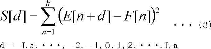
図6は、図1に示すデジタルカメラの位相差AF動作の変形例を説明するためのフローチャートである。図6において図5と同じ処理には同一符号を付して説明を省略する。
ステップS1の後、デフォーカス量算出部19は、ステップS1において取得した情報と、メインメモリ16に記憶されているテーブルとを用いてシフト量Lを仮決定する(ステップS10)。
続いて、デフォーカス量算出部19は、メインメモリ16に記憶された撮像画像信号のうち、画素行L1から得られた撮像用画素51の出力信号群と、画素行L2から得られた撮像用画素51の出力信号群を取得する(ステップS11)。
次に、デフォーカス量算出部19は、ステップS11で取得した2つの出力信号群と式(3)を用いて、ローリングシャッタによる位相差Dを算出する(ステップS12)。
次に、デフォーカス量算出部19は、ステップS10で仮決定したシフト量Lに、ステップS12で算出した位相差Dを加算した値をシフト量L’とする(ステップS13)。
次に、デフォーカス量算出部19は、ステップS3の処理を行い、ステップS3で取得した出力信号を用いて式(2)の演算を行い、S[d]が最小となったときのdを位相差量として算出する(ステップS14)。
デフォーカス量算出部19は、ステップS3,S14の処理を、位相差検出用画素51Rとこれとペア画素を構成する位相差検出用画素51Lを含む2つの画素行毎に行って、複数の位相差量を算出する。
デフォーカス量算出部19は、この複数の位相差量を用いてデフォーカス量を算出する(ステップS5)。その後、このデフォーカス量に基づいて合焦制御が行われる(ステップS6)。
以上のように、第一の変形例によれば、相関演算を行う対象となる2つの像の間に、ローリングシャッタ駆動による歪みが発生していた場合でも、デフォーカス量の算出を精度良く行うことができる。
なお、図6では、ステップS11とステップS3において、いずれも画素行L1,L2から得られた出力信号を取得している。このようにすることで、位相差AF時に、位相差検出用画素51R,51Lを含む画素行以外の画素行、つまり撮像用画素51だけを含む画素行からの信号読出しが不要となる。したがって、位相差AFに使用する信号の読み出しを高速化することができ、位相差AFの高速化が可能となる。
なお、ローリングシャッタ駆動に起因する位相差Dを算出するために用いる2つの出力信号群は、撮像用画素51だけを含む画素行から得られたものを用いてもよい。
例えば、図6のステップS11では、図3に示した画素行L3と画素行L4の各々から得られた出力信号群を用いて相関演算を行い、位相差Dを算出してもよい。
また、位相差Dを算出するために用いる2つの出力信号群は、近接する2つの画素行から得られたものであればよく、例えば、図3に示した画素行L3と画素行L5の各々から得られた出力信号群を用いて、位相差Dを算出してもよい。
この場合、デフォーカス量算出部19は、式(3)の左辺が最小となるようなdの値を位相差Dとして求めるが、ここで求まるDの値は、画素行L3と画素行L4の各々から得られた出力信号群を用いて算出した位相差Dの4倍の値となる。そのため、式(3)の左辺が最小となるようなdの値を4で割って得られる値を最終的な位相差Dとすればよい。
なお、この第一の変形例では、F値、焦点距離、及びフォーカス位置に応じてシフト量Lを仮決定し、その後、このシフト量Lに位相差Dを加算することで最終的なシフト量L’を求めた。
しかし、仮決定するシフト量Lは、F値、焦点距離、及びフォーカス位置によらずに固定の値としてもよい。このようにした場合、被写体のボケ状態に応じて相関演算を最適化できるという効果は得られないものの、ローリングシャッタ駆動に起因する画像の歪みを考慮して相関演算を行うことができる。このため、位相差AFの精度を向上させることが可能である。
なお、以上の説明では、固体撮像素子5に含まれる全ての画素行について、露光期間をずらすローリングシャッタ駆動を行うものとした。しかし、全ての画素行のうちの一部、つまり、位相差検出用画素51R,51Lを含む行についてだけ、ローリングシャッタ駆動し、それ以外の画素行についてはグローバルシャッタ駆動を行うといった形態も可能である。
ここまでは、画素51がいわゆるハニカム配列されたものを例にしたが、画素51が正方格子状に配列された固体撮像素子にも本発明は適用可能である。
図7は、図2に示す固体撮像素子5の変形例である固体撮像素子5aを示す図である。
固体撮像素子5aは、行方向Xと列方向Yに正方格子状に配列された多数の画素51’と、垂直走査回路52と、水平走査回路53とを備える。画素51’の構成は画素51と同じであり、カラーフィルタの配列はベイヤ配列となっている。
多数の画素51’は、遮光膜の開口aが偏心していない通常の画素51’と、偏心した開口d,eを有する位相差検出用画素とを含む。開口dを有する画素51’が位相差検出用画素51Lに対応し、開口eを有する画素51’が位相差検出用画素51Rに対応している。
このような構成の固体撮像素子5aでも、上述してきた方法でシフト量Lを決定することで、位相差AFを高速に行うことができる。
図2及び図7では、近接する位相差検出用画素51Rと位相差検出用画素51Lとで行方向Xの位置が1画素分ずれているが、近接する位相差検出用画素51Rと位相差検出用画素51Lの行方向Xの位置を同じにした構成としてもよい。
ここまでは、固体撮像素子5,5aが複数色のカラーフィルタを搭載してカラー撮像を行うものとしたが、固体撮像素子5,5aは、カラーフィルタを緑色の単色にする、カラーフィルタを省略する等して、モノクロ撮像用の撮像素子としてもよい。
また、第一の変形例以外の形態は、固体撮像素子5としてCCD型のものを用いることも可能である。
また、以上の説明では、固体撮像素子5を、撮像用画素51と位相差検出用画素51R,51Lが混在する撮像兼位相差検出用の撮像素子とした。しかし、撮像用画素51を持たない位相差AF専用の素子を固体撮像素子5とは別にカメラ内に設け、この素子からの出力信号を用いることでも、図5に示した位相差AFの処理を実施することができる。
また、以上の説明では、デフォーカス量算出部19が、F値、焦点距離、及びフォーカス位置に応じてシフト量Lを決めるものとした。しかし、これらのうちの1つに応じてシフト量Lを決める構成としても、位相差AFのための演算を効率的に行うことができる。
本明細書では撮像装置としてデジタルカメラを例にしたが、以下では、撮像装置としてカメラ付のスマートフォンの実施形態について説明する。
図8は、本発明の撮影装置の一実施形態であるスマートフォン200の外観を示すものである。図8に示すスマートフォン200は、平板状の筐体201を有し、筐体201の一方の面に表示部としての表示パネル202と、入力部としての操作パネル203とが一体となった表示入力部204を備えている。また、この様な筐体201は、スピーカ205と、マイクロホン206と、操作部207と、カメラ部208とを備えている。なお、筐体201の構成はこれに限定されず、例えば、表示部と入力部とが独立した構成を採用したり、折り畳み構造やスライド機構を有する構成を採用したりすることもできる。
図9は、図8に示すスマートフォン200の構成を示すブロック図である。図8に示すように、スマートフォンの主たる構成要素として、無線通信部210と、表示入力部204と、通話部211と、操作部207と、カメラ部208と、記憶部212と、外部入出力部213と、GPS(Global Positioning System)受信部214と、モーションセンサ部215と、電源部216と、主制御部220とを備える。また、スマートフォン200の主たる機能として、図示省略の基地局装置BSと図示省略の移動通信網NWとを介した移動無線通信を行う無線通信機能を備える。
無線通信部210は、主制御部220の指示にしたがって、移動通信網NWに収容された基地局装置BSに対し無線通信を行うものである。この無線通信を使用して、音声データ、画像データ等の各種ファイルデータ、電子メールデータなどの送受信や、Webデータやストリーミングデータなどの受信を行う。
表示入力部204は、主制御部220の制御により、画像(静止画像及び動画像)や文字情報などを表示して視覚的にユーザに情報を伝達するとともに、表示した情報に対するユーザ操作を検出する、いわゆるタッチパネルであって、表示パネル202と、操作パネル203とを備える。
表示パネル202は、LCD(Liquid Crystal Display)、OELD(Organic Electro-Luminescence Display)などを表示デバイスとして用いたものである。
操作パネル203は、表示パネル202の表示面上に表示される画像を視認可能に載置され、ユーザの指や尖筆によって操作される一又は複数の座標を検出するデバイスである。このデバイスをユーザの指や尖筆によって操作すると、操作に起因して発生する検出信号を主制御部220に出力する。次いで、主制御部220は、受信した検出信号に基づいて、表示パネル202上の操作位置(座標)を検出する。
図8に示すように、本発明の撮影装置の一実施形態として例示しているスマートフォン200の表示パネル202と操作パネル203とは一体となって表示入力部204を構成しているが、操作パネル203が表示パネル202を完全に覆うような配置となっている。
係る配置を採用した場合、操作パネル203は、表示パネル202外の領域についても、ユーザ操作を検出する機能を備えてもよい。換言すると、操作パネル203は、表示パネル202に重なる重畳部分についての検出領域(以下、表示領域と称する)と、それ以外の表示パネル202に重ならない外縁部分についての検出領域(以下、非表示領域と称する)とを備えていてもよい。
なお、表示領域の大きさと表示パネル202の大きさとを完全に一致させても良いが、両者を必ずしも一致させる必要は無い。また、操作パネル203が、外縁部分と、それ以外の内側部分の2つの感応領域を備えていてもよい。更に、外縁部分の幅は、筐体201の大きさなどに応じて適宜設計されるものである。更にまた、操作パネル203で採用される位置検出方式としては、マトリクススイッチ方式、抵抗膜方式、表面弾性波方式、赤外線方式、電磁誘導方式、静電容量方式などが挙げられ、いずれの方式を採用することもできる。
通話部211は、スピーカ205やマイクロホン206を備え、マイクロホン206を通じて入力されたユーザの音声を主制御部220にて処理可能な音声データに変換して主制御部220に出力したり、無線通信部210あるいは外部入出力部213により受信された音声データを復号してスピーカ205から出力させたりするものである。また、図8に示すように、例えば、スピーカ205を表示入力部204が設けられた面と同じ面に搭載し、マイクロホン206を筐体201の側面に搭載することができる。
操作部207は、キースイッチなどを用いたハードウェアキーであって、ユーザからの指示を受け付けるものである。例えば、図8に示すように、操作部207は、スマートフォン200の筐体201の側面に搭載され、指などで押下されるとオンとなり、指を離すとバネなどの復元力によってオフ状態となる押しボタン式のスイッチである。
記憶部212は、主制御部220の制御プログラムや制御データ、アプリケーションソフトウェア、通信相手の名称や電話番号などを対応づけたアドレスデータ、送受信した電子メールのデータ、WebブラウジングによりダウンロードしたWebデータや、ダウンロードしたコンテンツデータを記憶し、またストリーミングデータなどを一時的に記憶するものである。また、記憶部212は、スマートフォン内蔵の内部記憶部217と着脱自在な外部メモリスロットを有する外部記憶部218により構成される。なお、記憶部212を構成するそれぞれの内部記憶部217と外部記憶部218は、フラッシュメモリタイプ(flash memory type)、ハードディスクタイプ(hard disk type)、マルチメディアカードマイクロタイプ(multimedia card micro type)、カードタイプのメモリ(例えば、MicroSD(登録商標)メモリ等)、RAM(Random Access Memory)、ROM(Read Only Memory)などの格納媒体を用いて実現される。
外部入出力部213は、スマートフォン200に連結される全ての外部機器とのインターフェースの役割を果たすものであり、他の外部機器に通信等(例えば、ユニバーサルシリアルバス(USB)、IEEE1394など)又はネットワーク(例えば、インターネット、無線LAN、ブルートゥース(Bluetooth)(登録商標)、RFID(Radio Frequency Identification)、赤外線通信(Infrared Data Association:IrDA)(登録商標)、UWB(Ultra Wideband)(登録商標)、ジグビー(ZigBee)(登録商標)など)により直接的又は間接的に接続するためのものである。
スマートフォン200に連結される外部機器としては、例えば、有/無線ヘッドセット、有/無線外部充電器、有/無線データポート、カードソケットを介して接続されるメモリカード(Memory card)やSIM(Subscriber Identity Module Card)/UIM(User Identity Module Card)カード、オーディオ・ビデオI/O(Input/Output)端子を介して接続される外部オーディオ・ビデオ機器、無線接続される外部オーディオ・ビデオ機器、有/無線接続されるスマートフォン、有/無線接続されるパーソナルコンピュータ、有/無線接続されるPDA、有/無線接続されるパーソナルコンピュータ、イヤホンなどがある。外部入出力部213は、このような外部機器から伝送を受けたデータをスマートフォン200の内部の各構成要素に伝達することや、スマートフォン200の内部のデータが外部機器に伝送されるようにすることができる。
GPS受信部214は、主制御部220の指示にしたがって、GPS衛星ST1~STnから送信されるGPS信号を受信し、受信した複数のGPS信号に基づく測位演算処理を実行し、当該スマートフォン200の緯度、経度、高度からなる位置を検出する。GPS受信部214は、無線通信部210や外部入出力部213(例えば、無線LAN)から位置情報を取得できる時には、その位置情報を用いて位置を検出することもできる。
モーションセンサ部215は、例えば、3軸の加速度センサなどを備え、主制御部220の指示にしたがって、スマートフォン200の物理的な動きを検出する。スマートフォン200の物理的な動きを検出することにより、スマートフォン200の動く方向や加速度が検出される。係る検出結果は、主制御部220に出力されるものである。
電源部216は、主制御部220の指示にしたがって、スマートフォン200の各部に、バッテリ(図示しない)に蓄えられる電力を供給するものである。
主制御部220は、マイクロプロセッサを備え、記憶部212が記憶する制御プログラムや制御データにしたがって動作し、スマートフォン200の各部を統括して制御するものである。また、主制御部220は、無線通信部210を通じて、音声通信やデータ通信を行うために、通信系の各部を制御する移動通信制御機能と、アプリケーション処理機能を備える。
アプリケーション処理機能は、記憶部212が記憶するアプリケーションソフトウェアにしたがって主制御部220が動作することにより実現するものである。アプリケーション処理機能としては、例えば、外部入出力部213を制御して対向機器とデータ通信を行う赤外線通信機能や、電子メールの送受信を行う電子メール機能、Webページを閲覧するWebブラウジング機能などがある。
また、主制御部220は、受信データやダウンロードしたストリーミングデータなどの画像データ(静止画像や動画像のデータ)に基づいて、映像を表示入力部204に表示する等の画像処理機能を備える。画像処理機能とは、主制御部220が、上記画像データを復号し、この復号結果に画像処理を施して、画像を表示入力部204に表示する機能のことをいう。
更に、主制御部220は、表示パネル202に対する表示制御と、操作部207、操作パネル203を通じたユーザ操作を検出する操作検出制御を実行する。表示制御の実行により、主制御部220は、アプリケーションソフトウェアを起動するためのアイコンや、スクロールバーなどのソフトウェアキーを表示したり、あるいは電子メールを作成したりするためのウィンドウを表示する。なお、スクロールバーとは、表示パネル202の表示領域に収まりきれない大きな画像などについて、画像の表示部分を移動する指示を受け付けるためのソフトウェアキーのことをいう。
また、操作検出制御の実行により、主制御部220は、操作部207を通じたユーザ操作を検出したり、操作パネル203を通じて、上記アイコンに対する操作や、上記ウィンドウの入力欄に対する文字列の入力を受け付けたり、あるいは、スクロールバーを通じた表示画像のスクロール要求を受け付ける。
更に、操作検出制御の実行により主制御部220は、操作パネル203に対する操作位置が、表示パネル202に重なる重畳部分(表示領域)か、それ以外の表示パネル202に重ならない外縁部分(非表示領域)かを判定し、操作パネル203の感応領域や、ソフトウェアキーの表示位置を制御するタッチパネル制御機能を備える。
また、主制御部220は、操作パネル203に対するジェスチャ操作を検出し、検出したジェスチャ操作に応じて、予め設定された機能を実行することもできる。ジェスチャ操作とは、従来の単純なタッチ操作ではなく、指などによって軌跡を描いたり、複数の位置を同時に指定したり、あるいはこれらを組み合わせて、複数の位置から少なくとも1つについて軌跡を描く操作を意味する。
カメラ部208は、図1に示したデジタルカメラにおける外部メモリ制御部20、記録媒体21、表示制御部22、表示部23、及び操作部14以外の構成を含む。カメラ部208によって生成された撮像画像データは、記憶部212に記録したり、入出力部213や無線通信部210を通じて出力したりすることができる。図8に示すスマートフォン200において、カメラ部208は表示入力部204と同じ面に搭載されているが、カメラ部208の搭載位置はこれに限らず、表示入力部204の背面に搭載されてもよい。
また、カメラ部208はスマートフォン200の各種機能に利用することができる。例えば、表示パネル202にカメラ部208で取得した画像を表示することや、操作パネル203の操作入力のひとつとして、カメラ部208の画像を利用することができる。また、GPS受信部214が位置を検出する際に、カメラ部208からの画像を参照して位置を検出することもできる。更には、カメラ部208からの画像を参照して、3軸の加速度センサを用いずに、或いは、3軸の加速度センサと併用して、スマートフォン200のカメラ部208の光軸方向を判断することや、現在の使用環境を判断することもできる。勿論、カメラ部208からの画像をアプリケーションソフトウェア内で利用することもできる。
その他、静止画又は動画の画像データにGPS受信部214により取得した位置情報、マイクロホン206により取得した音声情報(主制御部等により、音声テキスト変換を行ってテキスト情報となっていてもよい)、モーションセンサ部215により取得した姿勢情報等などを付加して記録部212に記録したり、入出力部213や無線通信部210を通じて出力したりすることもできる。
以上のような構成のスマートフォン200においても、カメラ部208の撮像素子として固体撮像素子5,5aを用い、主制御部220において図5,6に例示した処理を行うことで、高速高精度の位相差AFが可能になる。
以上説明してきたように、本明細書には以下の事項が開示されている。
開示された撮像装置は、撮像光学系の瞳領域の異なる部分を通過した一対の光束の一方を受光する行方向に配列された複数の第一の位相差検出用の画素、及び、上記一対の光束の他方を受光する上記行方向に配列された複数の第二の位相差検出用の画素を含むセンサと、上記複数の第一の位相差検出用の画素の第一の出力信号群と、上記複数の第二の位相差検出用の画素の第二の出力信号群とを上記行方向に任意の量ずつずらしながら上記第一の出力信号群と上記第二の出力信号群との相関量を演算し、上記相関量が最大となるときの上記第一の出力信号群と上記第二の出力信号群の第一のずれ量からデフォーカス量を算出するデフォーカス量算出部と、上記デフォーカス量に基づいて上記撮像光学系の合焦状態を制御する合焦制御部と、を備え、上記デフォーカス量算出部は、上記第一の出力信号群と上記第二の出力信号群のずらし量の上限値を、上記撮像光学系のF値、上記撮像光学系の焦点距離、又は上記撮像光学系に含まれるフォーカスレンズの位置の少なくとも1つに応じて変更するものである。
開示された撮像装置は、上記センサが、上記撮像光学系の瞳領域を通過した光束を受光する上記行方向とこれに直交する列方向に二次元状に配列された複数の撮像用の画素を含む撮像兼位相差検出用の撮像素子であり、上記第一の位相差検出用の画素と上記第二の位相差検出用の画素とは異なる行に配置されており、上記画素の行毎に露光期間をずらし、各行に含まれる画素から、上記露光期間中の受光量に応じた信号を読み出すローリングシャッタ駆動を行う駆動部と、近接する2つの上記行の各々に含まれる複数の上記撮像用画素の出力信号群同士の相関量が最大となるときのその出力信号群同士の上記行方向におけるずれ量から、上記ローリングシャッタ駆動に起因する上記第一の出力信号群と上記第二の出力信号群との上記行方向における第二のずれ量を算出するずれ量算出部と、を備え、上記デフォーカス量算出部は、上記F値、上記焦点距離、又は上記フォーカスレンズの位置の少なくとも1つと上記第二のずれ量とに応じて上記ずらし量の上限値を変更するものである。
開示された撮像装置は、上記デフォーカス量算出部が、上記F値、上記焦点距離、又は上記フォーカスレンズの位置の少なくとも1つに応じて決めた上記上限値に上記第二のずれ量を加算した値を、最終的な上記ずらし量の上限値として決定するものである。
開示された撮像装置は、上記ずれ量算出部が、上記近接する2つの行として、上記第一の出力信号群の出力元である位相差検出用の画素と上記撮像用画素を含む行と、上記第二の出力信号群の出力元である位相差検出用の画素と上記撮像用画素を含む行を選択するものである。
開示された合焦制御方法は、撮像光学系の瞳領域の異なる部分を通過した一対の光束の一方を受光する行方向に配列された複数の第一の位相差検出用の画素、及び、上記一対の光束の他方を受光する上記行方向に配列された複数の第二の位相差検出用の画素を含むセンサを有する撮像装置における合焦制御方法であって、上記複数の第一の位相差検出用の画素の第一の出力信号群と、上記複数の第二の位相差検出用の画素の第二の出力信号群とを上記行方向に任意のずらし量ずつずらしながら上記第一の出力信号群と上記第二の出力信号群との相関量を演算し、上記相関量が最大となるときの上記第一の出力信号群と上記第二の出力信号群のずれ量からデフォーカス量を算出するデフォーカス量算出ステップと、上記デフォーカス量に基づいて上記撮像光学系の合焦状態を制御する合焦制御ステップと、を備え、上記デフォーカス量算出ステップでは、上記第一の出力信号群と上記第二の出力信号群のずらし量の上限値を、上記撮像光学系のF値、上記撮像光学系の焦点距離、又は上記撮像光学系に含まれるフォーカスレンズの位置の少なくとも1つに応じて変更するものである。
開示された撮像装置は、行方向とこれに直交する列方向に二次元状に配置された複数の画素を有し、上記複数の画素が、撮像光学系の瞳領域を通過した光束を受光する複数の撮像用画素、上記撮像光学系の瞳領域の異なる部分を通過した一対の光束の一方を受光する複数の第一の位相差検出用の画素、及び上記一対の光束の他方を受光する複数の第二の位相差検出用の画素を含む撮像素子と、上記画素の行毎に露光期間をずらし、各行に含まれる画素から、上記露光期間中の受光量に応じた信号を読み出すローリングシャッタ駆動を行う駆動部と、上記画素の行のうちの近接する2つの行の一方に含まれる複数の上記第一の位相差検出用の画素の第一の出力信号群と、上記2つの行の他方に含まれる複数の上記第二の位相差検出用の画素の第二の出力信号群とを上記行方向に任意の量ずつずらしながら上記第一の出力信号群と上記第二の出力信号群との相関量を演算し、上記相関量が最大となるときの上記第一の出力信号群と上記第二の出力信号群の第一のずれ量からデフォーカス量を算出するデフォーカス量算出部と、上記デフォーカス量に基づいて上記撮像光学系の合焦状態を制御する合焦制御部と、上記画素の行のうちの近接する2つの行の各々に含まれる複数の上記撮像用画素の出力信号群同士の相関量が最大となるときのその出力信号群同士の上記行方向におけるずれ量から、上記ローリングシャッタ駆動に起因する上記第一の出力信号群と上記第二の出力信号群との上記行方向における第二のずれ量を算出するずれ量算出部と、を備え、上記デフォーカス量算出部は、上記第一の出力信号群と上記第二の出力信号群のずらし量の上限値を、上記第二のずれ量に応じて変更するものである。
開示された撮像装置は、上記デフォーカス量算出部が、予め決められた値に上記第二のずれ量を加算した値を、上記ずらし量の上限値として決定するものである。
開示された撮像装置は、上記ずれ量算出部が、上記相関量を求める2つの行として、上記第一の出力信号群の出力元である位相差検出用の画素と上記撮像用画素を含む行と、上記第二の出力信号群の出力元である位相差検出用の画素と上記撮像用画素を含む行を選択するものである。
開示された合焦制御方法は、行方向とこれに直交する列方向に二次元状に配置された複数の画素を有し、上記複数の画素が、撮像光学系の瞳領域を通過した光束を受光する複数の撮像用画素、上記撮像光学系の瞳領域の異なる部分を通過した一対の光束の一方を受光する複数の第一の位相差検出用の画素、及び上記一対の光束の他方を受光する複数の第二の位相差検出用の画素を含む撮像素子を有する撮像装置による合焦制御方法であって、上記画素の行毎に露光期間をずらし、各行に含まれる画素から、上記露光期間中の受光量に応じた信号を読み出すローリングシャッタ駆動を行う駆動ステップと、上記画素の行のうちの近接する2つの行の一方に含まれる複数の上記第一の位相差検出用の画素の第一の出力信号群と、上記2つの行の他方に含まれる複数の上記第二の位相差検出用の画素の第二の出力信号群とを上記行方向に任意の量ずつずらしながら上記第一の出力信号群と上記第二の出力信号群との相関量を演算し、上記相関量が最大となるときの上記第一の出力信号群と上記第二の出力信号群の第一のずれ量からデフォーカス量を算出するデフォーカス量算出ステップと、上記デフォーカス量に基づいて上記撮像光学系の合焦状態を制御する合焦制御ステップと、上記画素の行のうちの近接する2つの行の各々に含まれる複数の上記撮像用画素の出力信号群同士の相関量が最大となるときのその出力信号群同士の上記行方向におけるずれ量から、上記ローリングシャッタ駆動に起因する上記第一の出力信号群と上記第二の出力信号群との上記行方向における第二のずれ量を算出するずれ量算出ステップと、を備え、上記デフォーカス量算出ステップでは、上記第一の出力信号群と上記第二の出力信号群のずらし量の上限値を、上記第二のずれ量に応じて変更するものである。
本発明によれば、位相差量の演算を効率的に行って位相差AFの速度を高速化することのできる撮像装置及び合焦制御方法を提供することができる。
以上、本発明を特定の実施形態によって説明したが、本発明はこの実施形態に限定されるものではなく、開示された発明の技術思想を逸脱しない範囲で種々の変更が可能である。
本出願は、2012年9月6日出願の日本特許出願(特願2012-196094)に基づくものであり、その内容はここに取り込まれる。
本出願は、2012年9月6日出願の日本特許出願(特願2012-196094)に基づくものであり、その内容はここに取り込まれる。
5 固体撮像素子
19 デフォーカス量算出部
51 画素
51R,51L 位相差検出用画素
19 デフォーカス量算出部
51 画素
51R,51L 位相差検出用画素
Claims (9)
- 撮像光学系の瞳領域の異なる部分を通過した一対の光束の一方を受光する行方向に配列された複数の第一の位相差検出用の画素、及び、前記一対の光束の他方を受光する前記行方向に配列された複数の第二の位相差検出用の画素を含むセンサと、
前記複数の第一の位相差検出用の画素の第一の出力信号群と、前記複数の第二の位相差検出用の画素の第二の出力信号群とを前記行方向に任意の量ずつずらしながら前記第一の出力信号群と前記第二の出力信号群との相関量を演算し、前記相関量が最大となるときの前記第一の出力信号群と前記第二の出力信号群の第一のずれ量からデフォーカス量を算出するデフォーカス量算出部と、
前記デフォーカス量に基づいて前記撮像光学系の合焦状態を制御する合焦制御部と、を備え、
前記デフォーカス量算出部は、前記第一の出力信号群と前記第二の出力信号群のずらし量の上限値を、前記撮像光学系のF値、前記撮像光学系の焦点距離、又は前記撮像光学系に含まれるフォーカスレンズの位置の少なくとも1つに応じて変更する撮像装置。 - 請求項1記載の撮像装置であって、
前記センサは、前記撮像光学系の瞳領域を通過した光束を受光する前記行方向とこれに直交する列方向に二次元状に配列された複数の撮像用の画素を含む撮像兼位相差検出用の撮像素子であり、
前記第一の位相差検出用の画素と前記第二の位相差検出用の画素とは異なる行に配置されており、
前記画素の行毎に露光期間をずらし、各行に含まれる画素から、前記露光期間中の受光量に応じた信号を読み出すローリングシャッタ駆動を行う駆動部と、
近接する2つの前記行の各々に含まれる複数の前記撮像用画素の出力信号群同士の相関量が最大となるときの当該出力信号群同士のずれ量から、前記ローリングシャッタ駆動に起因する前記第一の出力信号群と前記第二の出力信号群との前記行方向における第二のずれ量を算出するずれ量算出部と、を備え、
前記デフォーカス量算出部は、前記F値、前記焦点距離、又は前記フォーカスレンズの位置の少なくとも1つと前記第二のずれ量とに応じて前記ずらし量の上限値を変更する撮像装置。 - 請求項2記載の撮像装置であって、
前記デフォーカス量算出部は、前記F値、前記焦点距離、又は前記フォーカスレンズの位置の少なくとも1つに応じて決めた前記上限値に前記第二のずれ量を加算した値を、最終的な前記ずらし量の上限値として決定する撮像装置。 - 請求項2又は3記載の撮像装置であって、
前記ずれ量算出部は、前記近接する2つの行として、前記第一の出力信号群の出力元である位相差検出用の画素と前記撮像用画素を含む行と、前記第二の出力信号群の出力元である位相差検出用の画素と前記撮像用画素を含む行を選択する撮像装置。 - 撮像光学系の瞳領域の異なる部分を通過した一対の光束の一方を受光する行方向に配列された複数の第一の位相差検出用の画素、及び、前記一対の光束の他方を受光する前記行方向に配列された複数の第二の位相差検出用の画素を含むセンサを有する撮像装置における合焦制御方法であって、
前記複数の第一の位相差検出用の画素の第一の出力信号群と、前記複数の第二の位相差検出用の画素の第二の出力信号群とを前記行方向に任意のずらし量ずつずらしながら前記第一の出力信号群と前記第二の出力信号群との相関量を演算し、前記相関量が最大となるときの前記第一の出力信号群と前記第二の出力信号群のずれ量からデフォーカス量を算出するデフォーカス量算出ステップと、
前記デフォーカス量に基づいて前記撮像光学系の合焦状態を制御する合焦制御ステップと、を備え、
前記デフォーカス量算出ステップでは、前記第一の出力信号群と前記第二の出力信号群のずらし量の上限値を、前記撮像光学系のF値、前記撮像光学系の焦点距離、又は前記撮像光学系に含まれるフォーカスレンズの位置の少なくとも1つに応じて変更する合焦制御方法。 - 行方向とこれに直交する列方向に二次元状に配置された複数の画素を有し、前記複数の画素が、撮像光学系の瞳領域を通過した光束を受光する複数の撮像用画素、前記撮像光学系の瞳領域の異なる部分を通過した一対の光束の一方を受光する複数の第一の位相差検出用の画素、及び前記一対の光束の他方を受光する複数の第二の位相差検出用の画素を含む撮像素子と、
前記画素の行毎に露光期間をずらし、各行に含まれる画素から、前記露光期間中の受光量に応じた信号を読み出すローリングシャッタ駆動を行う駆動部と、
前記画素の行のうちの近接する2つの行の一方に含まれる複数の前記第一の位相差検出用の画素の第一の出力信号群と、前記2つの行の他方に含まれる複数の前記第二の位相差検出用の画素の第二の出力信号群とを前記行方向に任意の量ずつずらしながら前記第一の出力信号群と前記第二の出力信号群との相関量を演算し、前記相関量が最大となるときの前記第一の出力信号群と前記第二の出力信号群の第一のずれ量からデフォーカス量を算出するデフォーカス量算出部と、
前記デフォーカス量に基づいて前記撮像光学系の合焦状態を制御する合焦制御部と、
前記画素の行のうちの近接する2つの行の各々に含まれる複数の前記撮像用画素の出力信号群同士の相関量が最大となるときの当該出力信号群同士の前記行方向におけるずれ量から、前記ローリングシャッタ駆動に起因する前記第一の出力信号群と前記第二の出力信号群との前記行方向における第二のずれ量を算出するずれ量算出部と、を備え、
前記デフォーカス量算出部は、前記第一の出力信号群と前記第二の出力信号群のずらし量の上限値を、前記第二のずれ量に応じて変更する撮像装置。 - 請求項6記載の撮像装置であって、
前記デフォーカス量算出部は、予め決められた値に前記第二のずれ量を加算した値を、前記ずらし量の上限値として決定する撮像装置。 - 請求項6又は7記載の撮像装置であって、
前記ずれ量算出部は、前記相関量を求める2つの行として、前記第一の出力信号群の出力元である位相差検出用の画素と前記撮像用画素を含む行と、前記第二の出力信号群の出力元である位相差検出用の画素と前記撮像用画素を含む行を選択する撮像装置。 - 行方向とこれに直交する列方向に二次元状に配置された複数の画素を有し、前記複数の画素が、撮像光学系の瞳領域を通過した光束を受光する複数の撮像用画素、前記撮像光学系の瞳領域の異なる部分を通過した一対の光束の一方を受光する複数の第一の位相差検出用の画素、及び前記一対の光束の他方を受光する複数の第二の位相差検出用の画素を含む撮像素子を有する撮像装置による合焦制御方法であって、
前記画素の行毎に露光期間をずらし、各行に含まれる画素から、前記露光期間中の受光量に応じた信号を読み出すローリングシャッタ駆動を行う駆動ステップと、
前記画素の行のうちの近接する2つの行の一方に含まれる複数の前記第一の位相差検出用の画素の第一の出力信号群と、前記2つの行の他方に含まれる複数の前記第二の位相差検出用の画素の第二の出力信号群とを前記行方向に任意の量ずつずらしながら前記第一の出力信号群と前記第二の出力信号群との相関量を演算し、前記相関量が最大となるときの前記第一の出力信号群と前記第二の出力信号群の第一のずれ量からデフォーカス量を算出するデフォーカス量算出ステップと、
前記デフォーカス量に基づいて前記撮像光学系の合焦状態を制御する合焦制御ステップと、
前記画素の行のうちの近接する2つの行の各々に含まれる複数の前記撮像用画素の出力信号群同士の相関量が最大となるときの当該出力信号群同士の前記行方向におけるずれ量から、前記ローリングシャッタ駆動に起因する前記第一の出力信号群と前記第二の出力信号群との前記行方向における第二のずれ量を算出するずれ量算出ステップと、を備え、
前記デフォーカス量算出ステップでは、前記第一の出力信号群と前記第二の出力信号群のずらし量の上限値を、前記第二のずれ量に応じて変更する合焦制御方法。
Priority Applications (3)
| Application Number | Priority Date | Filing Date | Title |
|---|---|---|---|
| JP2014534216A JP5750550B2 (ja) | 2012-09-06 | 2013-05-30 | 撮像装置及び合焦制御方法 |
| CN201380046604.3A CN104603662B (zh) | 2012-09-06 | 2013-05-30 | 摄像装置及对焦控制方法 |
| US14/640,858 US9432569B2 (en) | 2012-09-06 | 2015-03-06 | Imaging device and focus control method |
Applications Claiming Priority (2)
| Application Number | Priority Date | Filing Date | Title |
|---|---|---|---|
| JP2012-196094 | 2012-09-06 | ||
| JP2012196094 | 2012-09-06 |
Related Child Applications (1)
| Application Number | Title | Priority Date | Filing Date |
|---|---|---|---|
| US14/640,858 Continuation US9432569B2 (en) | 2012-09-06 | 2015-03-06 | Imaging device and focus control method |
Publications (1)
| Publication Number | Publication Date |
|---|---|
| WO2014038258A1 true WO2014038258A1 (ja) | 2014-03-13 |
Family
ID=50236881
Family Applications (1)
| Application Number | Title | Priority Date | Filing Date |
|---|---|---|---|
| PCT/JP2013/065022 Ceased WO2014038258A1 (ja) | 2012-09-06 | 2013-05-30 | 撮像装置及び合焦制御方法 |
Country Status (3)
| Country | Link |
|---|---|
| US (1) | US9432569B2 (ja) |
| JP (1) | JP5750550B2 (ja) |
| WO (1) | WO2014038258A1 (ja) |
Cited By (1)
| Publication number | Priority date | Publication date | Assignee | Title |
|---|---|---|---|---|
| EP3098638A1 (en) * | 2015-05-29 | 2016-11-30 | Phase One A/S | Adaptive autofocusing system |
Families Citing this family (9)
| Publication number | Priority date | Publication date | Assignee | Title |
|---|---|---|---|---|
| JP5973708B2 (ja) * | 2011-10-21 | 2016-08-23 | オリンパス株式会社 | 撮像装置及び内視鏡装置 |
| JP5775976B2 (ja) * | 2012-11-22 | 2015-09-09 | 富士フイルム株式会社 | 撮像装置、デフォーカス量演算方法、及び撮像光学系 |
| CN105074528B (zh) * | 2013-03-29 | 2017-07-18 | 富士胶片株式会社 | 摄像装置及对焦控制方法 |
| JP2015164284A (ja) * | 2014-01-28 | 2015-09-10 | キヤノン株式会社 | 固体撮像素子、動き情報取得装置、および撮像装置 |
| JP2016038414A (ja) * | 2014-08-05 | 2016-03-22 | キヤノン株式会社 | 焦点検出装置およびその制御方法、並びに撮像装置 |
| JP6765860B2 (ja) * | 2016-06-01 | 2020-10-07 | キヤノン株式会社 | 撮像素子、撮像装置、および撮像信号処理方法 |
| CN109937382B (zh) | 2016-08-26 | 2020-12-18 | 华为技术有限公司 | 成像装置和成像方法 |
| US11889207B2 (en) * | 2019-06-10 | 2024-01-30 | Sony Semiconductor Solutions Corporation | Solid-state imaging element, imaging device, and method for controlling solid-state imaging element |
| KR20230050011A (ko) * | 2021-10-07 | 2023-04-14 | 에스케이하이닉스 주식회사 | 카메라 테스트 장치, 및 카메라의 포커싱 특성을 테스트 하는 방법 |
Citations (3)
| Publication number | Priority date | Publication date | Assignee | Title |
|---|---|---|---|---|
| JP2009063952A (ja) * | 2007-09-10 | 2009-03-26 | Nikon Corp | 撮像素子、焦点検出装置および撮像装置 |
| JP2010139624A (ja) * | 2008-12-10 | 2010-06-24 | Nikon Corp | 撮像素子および撮像装置 |
| JP2012141549A (ja) * | 2011-01-06 | 2012-07-26 | Nikon Corp | 撮像装置 |
Family Cites Families (9)
| Publication number | Priority date | Publication date | Assignee | Title |
|---|---|---|---|---|
| JPH07143391A (ja) | 1993-11-12 | 1995-06-02 | Canon Inc | 静止画記録装置 |
| JP4468396B2 (ja) | 2001-04-24 | 2010-05-26 | キヤノン株式会社 | レンズユニット及びこれを有する光学機器 |
| JP4946313B2 (ja) * | 2006-09-27 | 2012-06-06 | 株式会社ニコン | 撮像装置 |
| JP4349407B2 (ja) * | 2006-11-17 | 2009-10-21 | ソニー株式会社 | 撮像装置 |
| JP5499432B2 (ja) | 2007-10-05 | 2014-05-21 | ソニー株式会社 | 撮像装置 |
| JP2010020015A (ja) * | 2008-07-09 | 2010-01-28 | Canon Inc | 撮像装置 |
| CN103380392B (zh) * | 2011-03-31 | 2014-12-03 | 富士胶片株式会社 | 摄像装置及其对焦控制方法 |
| JP5979849B2 (ja) * | 2011-11-21 | 2016-08-31 | キヤノン株式会社 | 撮像素子及び撮像装置 |
| JP6124564B2 (ja) * | 2012-11-21 | 2017-05-10 | キヤノン株式会社 | 焦点検出装置及び方法、及び撮像装置 |
-
2013
- 2013-05-30 JP JP2014534216A patent/JP5750550B2/ja active Active
- 2013-05-30 WO PCT/JP2013/065022 patent/WO2014038258A1/ja not_active Ceased
-
2015
- 2015-03-06 US US14/640,858 patent/US9432569B2/en active Active
Patent Citations (3)
| Publication number | Priority date | Publication date | Assignee | Title |
|---|---|---|---|---|
| JP2009063952A (ja) * | 2007-09-10 | 2009-03-26 | Nikon Corp | 撮像素子、焦点検出装置および撮像装置 |
| JP2010139624A (ja) * | 2008-12-10 | 2010-06-24 | Nikon Corp | 撮像素子および撮像装置 |
| JP2012141549A (ja) * | 2011-01-06 | 2012-07-26 | Nikon Corp | 撮像装置 |
Cited By (2)
| Publication number | Priority date | Publication date | Assignee | Title |
|---|---|---|---|---|
| EP3098638A1 (en) * | 2015-05-29 | 2016-11-30 | Phase One A/S | Adaptive autofocusing system |
| US10158796B2 (en) | 2015-05-29 | 2018-12-18 | Phase One A/S | Adaptive autofocusing system |
Also Published As
| Publication number | Publication date |
|---|---|
| US9432569B2 (en) | 2016-08-30 |
| JP5750550B2 (ja) | 2015-07-22 |
| US20150181108A1 (en) | 2015-06-25 |
| JPWO2014038258A1 (ja) | 2016-08-08 |
| CN104603662A (zh) | 2015-05-06 |
Similar Documents
| Publication | Publication Date | Title |
|---|---|---|
| JP5948492B2 (ja) | 撮像装置及び合焦制御方法 | |
| JP5750550B2 (ja) | 撮像装置及び合焦制御方法 | |
| JP5775976B2 (ja) | 撮像装置、デフォーカス量演算方法、及び撮像光学系 | |
| JP5690974B2 (ja) | 撮像装置及び合焦制御方法 | |
| JP5542249B2 (ja) | 撮像素子及びこれを用いた撮像装置及び撮像方法 | |
| JP5799178B2 (ja) | 撮像装置及び合焦制御方法 | |
| JP6031587B2 (ja) | 撮像装置、信号処理方法、信号処理プログラム | |
| JP5942043B2 (ja) | 撮像装置及び合焦制御方法 | |
| JP5779726B2 (ja) | 撮像装置及び露出決定方法 | |
| JP6307526B2 (ja) | 撮像装置及び合焦制御方法 | |
| JP5872122B2 (ja) | 撮像装置及び合焦制御方法 | |
| JP5978411B2 (ja) | 撮像装置及び合焦制御方法 | |
| JP5542248B2 (ja) | 撮像素子及び撮像装置 | |
| JP5677628B2 (ja) | 撮像装置及び撮像方法 | |
| CN104603662B (zh) | 摄像装置及对焦控制方法 | |
| WO2013145887A1 (ja) | 撮像装置及び撮像方法 |
Legal Events
| Date | Code | Title | Description |
|---|---|---|---|
| 121 | Ep: the epo has been informed by wipo that ep was designated in this application |
Ref document number: 13835401 Country of ref document: EP Kind code of ref document: A1 |
|
| ENP | Entry into the national phase |
Ref document number: 2014534216 Country of ref document: JP Kind code of ref document: A |
|
| NENP | Non-entry into the national phase |
Ref country code: DE |
|
| 122 | Ep: pct application non-entry in european phase |
Ref document number: 13835401 Country of ref document: EP Kind code of ref document: A1 |