WO2014034649A1 - 光変調器 - Google Patents
光変調器 Download PDFInfo
- Publication number
- WO2014034649A1 WO2014034649A1 PCT/JP2013/072837 JP2013072837W WO2014034649A1 WO 2014034649 A1 WO2014034649 A1 WO 2014034649A1 JP 2013072837 W JP2013072837 W JP 2013072837W WO 2014034649 A1 WO2014034649 A1 WO 2014034649A1
- Authority
- WO
- WIPO (PCT)
- Prior art keywords
- waveguide
- light
- optical modulator
- output
- substrate
- Prior art date
- Legal status (The legal status is an assumption and is not a legal conclusion. Google has not performed a legal analysis and makes no representation as to the accuracy of the status listed.)
- Ceased
Links
Images


Classifications
-
- G—PHYSICS
- G02—OPTICS
- G02F—OPTICAL DEVICES OR ARRANGEMENTS FOR THE CONTROL OF LIGHT BY MODIFICATION OF THE OPTICAL PROPERTIES OF THE MEDIA OF THE ELEMENTS INVOLVED THEREIN; NON-LINEAR OPTICS; FREQUENCY-CHANGING OF LIGHT; OPTICAL LOGIC ELEMENTS; OPTICAL ANALOGUE/DIGITAL CONVERTERS
- G02F1/00—Devices or arrangements for the control of the intensity, colour, phase, polarisation or direction of light arriving from an independent light source, e.g. switching, gating or modulating; Non-linear optics
- G02F1/01—Devices or arrangements for the control of the intensity, colour, phase, polarisation or direction of light arriving from an independent light source, e.g. switching, gating or modulating; Non-linear optics for the control of the intensity, phase, polarisation or colour
- G02F1/03—Devices or arrangements for the control of the intensity, colour, phase, polarisation or direction of light arriving from an independent light source, e.g. switching, gating or modulating; Non-linear optics for the control of the intensity, phase, polarisation or colour based on ceramics or electro-optical crystals, e.g. exhibiting Pockels effect or Kerr effect
- G02F1/035—Devices or arrangements for the control of the intensity, colour, phase, polarisation or direction of light arriving from an independent light source, e.g. switching, gating or modulating; Non-linear optics for the control of the intensity, phase, polarisation or colour based on ceramics or electro-optical crystals, e.g. exhibiting Pockels effect or Kerr effect in an optical waveguide structure
-
- G—PHYSICS
- G02—OPTICS
- G02F—OPTICAL DEVICES OR ARRANGEMENTS FOR THE CONTROL OF LIGHT BY MODIFICATION OF THE OPTICAL PROPERTIES OF THE MEDIA OF THE ELEMENTS INVOLVED THEREIN; NON-LINEAR OPTICS; FREQUENCY-CHANGING OF LIGHT; OPTICAL LOGIC ELEMENTS; OPTICAL ANALOGUE/DIGITAL CONVERTERS
- G02F1/00—Devices or arrangements for the control of the intensity, colour, phase, polarisation or direction of light arriving from an independent light source, e.g. switching, gating or modulating; Non-linear optics
- G02F1/01—Devices or arrangements for the control of the intensity, colour, phase, polarisation or direction of light arriving from an independent light source, e.g. switching, gating or modulating; Non-linear optics for the control of the intensity, phase, polarisation or colour
- G02F1/21—Devices or arrangements for the control of the intensity, colour, phase, polarisation or direction of light arriving from an independent light source, e.g. switching, gating or modulating; Non-linear optics for the control of the intensity, phase, polarisation or colour by interference
- G02F1/225—Devices or arrangements for the control of the intensity, colour, phase, polarisation or direction of light arriving from an independent light source, e.g. switching, gating or modulating; Non-linear optics for the control of the intensity, phase, polarisation or colour by interference in an optical waveguide structure
-
- G—PHYSICS
- G02—OPTICS
- G02B—OPTICAL ELEMENTS, SYSTEMS OR APPARATUS
- G02B6/00—Light guides; Structural details of arrangements comprising light guides and other optical elements, e.g. couplings
- G02B6/10—Light guides; Structural details of arrangements comprising light guides and other optical elements, e.g. couplings of the optical waveguide type
- G02B6/12—Light guides; Structural details of arrangements comprising light guides and other optical elements, e.g. couplings of the optical waveguide type of the integrated circuit kind
- G02B2006/12133—Functions
- G02B2006/12159—Interferometer
-
- G—PHYSICS
- G02—OPTICS
- G02F—OPTICAL DEVICES OR ARRANGEMENTS FOR THE CONTROL OF LIGHT BY MODIFICATION OF THE OPTICAL PROPERTIES OF THE MEDIA OF THE ELEMENTS INVOLVED THEREIN; NON-LINEAR OPTICS; FREQUENCY-CHANGING OF LIGHT; OPTICAL LOGIC ELEMENTS; OPTICAL ANALOGUE/DIGITAL CONVERTERS
- G02F1/00—Devices or arrangements for the control of the intensity, colour, phase, polarisation or direction of light arriving from an independent light source, e.g. switching, gating or modulating; Non-linear optics
- G02F1/01—Devices or arrangements for the control of the intensity, colour, phase, polarisation or direction of light arriving from an independent light source, e.g. switching, gating or modulating; Non-linear optics for the control of the intensity, phase, polarisation or colour
- G02F1/21—Devices or arrangements for the control of the intensity, colour, phase, polarisation or direction of light arriving from an independent light source, e.g. switching, gating or modulating; Non-linear optics for the control of the intensity, phase, polarisation or colour by interference
- G02F1/212—Mach-Zehnder type
-
- G—PHYSICS
- G02—OPTICS
- G02F—OPTICAL DEVICES OR ARRANGEMENTS FOR THE CONTROL OF LIGHT BY MODIFICATION OF THE OPTICAL PROPERTIES OF THE MEDIA OF THE ELEMENTS INVOLVED THEREIN; NON-LINEAR OPTICS; FREQUENCY-CHANGING OF LIGHT; OPTICAL LOGIC ELEMENTS; OPTICAL ANALOGUE/DIGITAL CONVERTERS
- G02F1/00—Devices or arrangements for the control of the intensity, colour, phase, polarisation or direction of light arriving from an independent light source, e.g. switching, gating or modulating; Non-linear optics
- G02F1/01—Devices or arrangements for the control of the intensity, colour, phase, polarisation or direction of light arriving from an independent light source, e.g. switching, gating or modulating; Non-linear optics for the control of the intensity, phase, polarisation or colour
- G02F1/21—Devices or arrangements for the control of the intensity, colour, phase, polarisation or direction of light arriving from an independent light source, e.g. switching, gating or modulating; Non-linear optics for the control of the intensity, phase, polarisation or colour by interference
- G02F1/225—Devices or arrangements for the control of the intensity, colour, phase, polarisation or direction of light arriving from an independent light source, e.g. switching, gating or modulating; Non-linear optics for the control of the intensity, phase, polarisation or colour by interference in an optical waveguide structure
- G02F1/2257—Devices or arrangements for the control of the intensity, colour, phase, polarisation or direction of light arriving from an independent light source, e.g. switching, gating or modulating; Non-linear optics for the control of the intensity, phase, polarisation or colour by interference in an optical waveguide structure the optical waveguides being made of semiconducting material
-
- G—PHYSICS
- G02—OPTICS
- G02F—OPTICAL DEVICES OR ARRANGEMENTS FOR THE CONTROL OF LIGHT BY MODIFICATION OF THE OPTICAL PROPERTIES OF THE MEDIA OF THE ELEMENTS INVOLVED THEREIN; NON-LINEAR OPTICS; FREQUENCY-CHANGING OF LIGHT; OPTICAL LOGIC ELEMENTS; OPTICAL ANALOGUE/DIGITAL CONVERTERS
- G02F2201/00—Constructional arrangements not provided for in groups G02F1/00 - G02F7/00
- G02F2201/58—Arrangements comprising a monitoring photodetector
Definitions
- the present invention relates to an optical modulator, and more particularly to an optical modulator having monitoring means for monitoring radiated light emitted from a multiplexing part of a Mach-Zehnder type waveguide.
- an optical modulator having a Mach-Zehnder type waveguide is used.
- a thin plate type optical modulator having a substrate thickness of 20 ⁇ m or less has been put into practical use.
- a higher-order mode propagates as unnecessary light in the vicinity of the optical waveguide. For this reason, the anti-phase interference light (radiated light) radiated at the multiplexing part of the Mach-Zehnder (MZ) waveguide is not easily separated from the main output waveguide, unlike the case where the substrate is thick.
- MZ Mach-Zehnder
- Patent Document 1 a method of using a three-branch structure having a structure of a multiplexing unit on the output side with a waveguide for anti-phase interference light guide, or around the branch waveguide as in Patent Document 2
- the anti-phase interference light (radiated light) is separated from the output waveguide by a method using a guide for anti-phase interference light.
- the anti-phase interference light is detected and used as a DC bias monitor for the optical modulator.
- Patent Document 3 discloses a structure for compensating the quality of the monitor output by synthesizing two radiated lights radiated from the multiplexing portion of the MZ type waveguide.
- minute antiphase interference light remains as a high-order mode in the vicinity of the output waveguide.
- the main output from the fiber is a combination of the in-phase interference output light and the anti-phase interference light.
- Patent Document 4 in order to remove the radiated light generated in the multiplexing part of the Mach-Zehnder type waveguide, a radiated light waveguide is provided in the multiplexing part, and a higher order mode is provided in the vicinity of the output waveguide. Forming a light absorption region is disclosed.
- Patent Document 4 does not disclose any configuration for maintaining an appropriate relationship between the monitor characteristic using the antiphase interference light (radiated light) and the main output characteristic. In other words, when radiated light is mixed into the main output light, not only the on / off characteristics but also the phase difference characteristics are affected. In particular, the phase difference characteristic varies greatly even if a small amount of radiated light is mixed into the main output light.
- phase difference varies by about 0.6%.
- the amount of phase difference required for the optical modulator needs to be 1% or less when a high quality monitor is required, and it is required that the mixing of radiated light into the main output light be very small. Is done.
- JP 2006-301612 A International Publication No. WO2006-090863 Japanese Patent Application No. 2011-037718 (Filing date: February 23, 2011) JP 2011-75906 A
- the problem to be solved by the present invention is to solve the above-mentioned problems, maintain the main output characteristic and the monitor characteristic in an appropriate relationship, and determine the bias point determined by the monitor output and the optimum bias point of the main output. It is an object to provide an optical modulator that can be matched and capable of highly accurate bias control.
- the optical modulator of the present invention has the following technical features.
- An optical waveguide is formed on a substrate having a thickness of 20 ⁇ m or less, and the optical waveguide guides signal light from a Mach-Zehnder type waveguide and a combining portion of the Mach-Zehnder type waveguide and outputs the signal light to the outside of the substrate.
- An optical modulator having an output waveguide for monitoring and a monitor means for monitoring the signal light or the emitted light, a part of the emitted light propagating through the output waveguide is removed from the output waveguide, and the substrate It is characterized by comprising leakage light removing means for emitting outside.
- the signal light emitted from the output waveguide is guided by an optical fiber disposed to face the end face of the substrate.
- the radiated light is radiated light output from the multiplexing unit when the signal light is in an off state.
- the leakage light removing unit is disposed in the vicinity of the output waveguide and continues to the vicinity of the end of the substrate. It is characterized by being a slab waveguide formed.
- the leakage light removing means is a light absorbing material disposed in the vicinity of the output waveguide.
- the monitoring unit includes a radiation optical waveguide branched from the multiplexing unit.
- the length of the leakage light removing unit along the output waveguide is 1 mm or less.
- an optical waveguide is formed on a substrate having a thickness of 20 ⁇ m or less, and the optical waveguide guides signal light from a Mach-Zehnder type waveguide and a combining portion of the Mach-Zehnder type waveguide.
- An optical modulator having an output waveguide for outputting to the outside and a monitor means for monitoring radiated light output from the multiplexing unit when the signal light is in an off state, and propagates through the output waveguide Since a leakage light removing means for removing a part of the radiated light from the output waveguide and emitting it out of the substrate is provided, the bias point determined by the monitor output matches the optimum bias point of the main output. Therefore, it is possible to provide an optical modulator capable of highly accurate bias control.
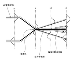
- FIG. 2 is a diagram for explaining a state of a light wave propagating from a multiplexing part of a Mach-Zehnder type waveguide in the optical modulator of FIG. 1 to leakage light removing means.
- an optical waveguide is formed on a substrate having a thickness of 20 ⁇ m or less, and the optical waveguide is a combination of a Mach-Zehnder (MZ) type waveguide and the Mach-Zehnder type waveguide.
- MZ Mach-Zehnder
- a leakage light removing means for removing a part of the light from the output waveguide and emitting it out of the substrate is provided.
- the substrate a substrate having an electro-optic effect such as lithium niobate or lithium tantalate can be used.
- the optical waveguide is formed by thermally diffusing a high refractive index substance such as titanium (Ti) on a lithium niobate substrate (LN substrate).
- a high refractive index substance such as titanium (Ti)
- LiN substrate lithium niobate substrate
- the substrate and the optical waveguide can be formed of a polymer.
- a high refractive index polymer having a convex portion in the core portion is disposed, and a low refractive index polymer is disposed as a clad on the upper and lower sides so as to sandwich the polymer, thereby producing a flat substrate having an optical waveguide.
- the optical modulator of the present invention uses a substrate such as lithium niobate having a substrate thickness of 20 ⁇ m or less.
- a substrate thickness of 20 ⁇ m or less For example, an LN wafer on which a Ti diffusion waveguide is formed is polished to 20 ⁇ m or less and used by being fixed to a holding substrate via an adhesive. Note that the substrate can be thinned even after the electrodes are formed.
- the electrodes such as the modulation electrode and the phase shift electrode can be formed by forming a seed layer to a thickness of about 100 nm by vapor deposition, sputtering, CVD, etc., and further forming it by a semi-additive method by electrolytic plating.
- At least one Mach-Zehnder (MZ) type waveguide is formed on a thin plate substrate, and a modulation electrode (not shown) is arranged along the MZ type waveguide.
- MZ Mach-Zehnder
- the in-phase interference light at the multiplexing portion of the MZ waveguide becomes the main output light, and the anti-phase interference light (radiated light) becomes the monitor output light.
- the feature of the present invention is that, as shown in FIG. 2, a high-order mode removal structure composed of a waveguide structure is provided as a leakage light removal means in the vicinity of the main output waveguide extending from the multiplexing portion, and the main output guide is provided.
- the anti-phase interference light remaining as a higher-order mode of the waveguide in the vicinity of the waveguide is removed.
- the removal structure is arranged close to the edge of the substrate.
- a three-branch structure is used for the multiplexing part.
- the light modulated by each action part (branch waveguide) of the Mach-Zehnder type waveguide interferes at the multiplexing part, and when it interferes in the same phase, the main output waveguide having a large width at the center of the output three-branch structure Is output.
- the main output waveguide having a large width at the center of the output three-branch structure Is output.
- most of the optical power is output to a narrow waveguide (radiated light waveguide) outside the three branches, but in the case of a thin plate structure A part of the power propagates as a higher-order mode of the central waveguide (main output waveguide). In order to remove this higher order mode, leakage light removing means is formed.
- the leakage light removing means is composed of a slab waveguide arranged in the vicinity of the output waveguide and continuously to the end of the substrate, or a light absorbing material arranged in the vicinity of the output waveguide. Is possible. In the case of a slab waveguide, it can be formed simultaneously with the process of forming another optical waveguide, and when the light absorbing material is made of the same material as the electrode, The light absorbing material can be formed at least partially.
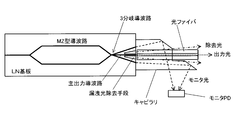
- the signal light (output light) emitted from the main output waveguide is guided to the outside by an optical fiber disposed facing the end face of the LN substrate.
- the leakage light removing means functions so that leakage light other than the main output light (high-order mode light, radiated light, etc.) is not mixed into the optical fiber.
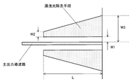
- FIG. 4 shows a state in which leakage light removing means is configured by a slab waveguide.
- the slab waveguide In order to couple the higher-order mode existing in the vicinity of the main output waveguide to the removal waveguide (slab waveguide), the slab waveguide is arranged close to the main waveguide.
- the removal waveguide (slab waveguide) also couples part of the fundamental mode light, which is signal light, at the same time as the higher-order mode, resulting in an output loss. Therefore, the interval W1 between the main output waveguide and the removal waveguide is set to about 1 to 2 times the mode field diameter of the fundamental mode light, and is set to 10 to 20 ⁇ m when using an optical waveguide formed by Ti diffusion on the LN substrate. To do.
- the length L of the removal waveguide (slab waveguide) close to the main output waveguide to 1 mm or less, not only the coupling of the fundamental mode light to the slab waveguide but also the high slab waveguide coupled It is possible to prevent a problem that the next mode is recoupled to the main output waveguide. As a result, it is possible to suppress the shift of the bias point while suppressing the excess loss to 0.5 dB or less.
- the input side of the removal waveguide (slab waveguide) has a structure that can suppress mode conversion due to structural discontinuity caused by the arrangement of the removal waveguide, and in FIG. 4, a structure that narrows the width W2 on the input side. It is said. Ideally, a width of 0 is desirable, but in that case, pattern formation in the photolithography process becomes difficult. Therefore, manufacturing reproducibility can be improved by setting W2 to about 1 to 2 ⁇ m.
- the removal waveguide is arranged up to the substrate end face or a region close to the end face.
- the width W3 between the outer boundary line of the removal waveguide at the end face and the main waveguide is set to 50 ⁇ m or less, the monitor light propagating through the three-branch waveguide and the removal light can be largely separated, and the removal light is mixed into the monitor light. Can be suppressed.
- the substrate end is perpendicular to the waveguide, but the end face may be inclined with respect to the waveguide in order to prevent reflected return of the guided light.
- a method using a capillary as a fiber holding member is illustrated in FIG. 3, but a fiber is connected to a monitor light waveguide (radiation light waveguide), or a light receiving element on the substrate end or on the waveguide.
- a method of arranging (PD) and extracting a signal directly from the waveguide for monitoring light may be used.
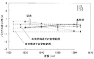
- FIG. 5 shows an example in which the wavelength dependence and temperature dependence of the shift of the bias point between the fiber output light and the monitor output are measured using the optical modulator having the structure shown in FIGS.
- the horizontal axis indicates the wavelength
- the vertical axis indicates the amount of bias point shift between the output and the monitor normalized by V ⁇ of the modulator.
- a solid line in the figure indicates a case where there is a leakage light removing unit and a case where there is no broken line.
- a bias point shift characteristic stable with respect to temperature and wavelength can be obtained.
- stable modulator bias control becomes possible, and a favorable modulator signal output can be obtained even when the wavelength or ambient temperature changes.
- FIG. 6 is a diagram for explaining another shape of the slab waveguide used for the leakage light removing means.
- FIG. 6A it is possible to employ a structure in which the removal portion gradually approaches the waveguide in order to reduce discontinuity on the input side.
- FIG. 6B it is also possible to adopt a structure in which the distance between the main output waveguide and the slab waveguide is gradually increased in order to suppress the coupling to the fiber on the output side.
- a material that gives light loss such as Au or Al may be used for the absorbing layer, or a refractive index higher than that of a substrate that is clad with a semiconductor material or the like. You may comprise so that it may take out from a waveguide board
- the main output characteristic and the monitor characteristic are maintained in an appropriate relationship, the bias point determined by the monitor output is matched with the optimum bias point of the main output, and the high-precision bias is obtained.
- An optical modulator that can be controlled can be provided.
Landscapes
- Physics & Mathematics (AREA)
- Nonlinear Science (AREA)
- General Physics & Mathematics (AREA)
- Optics & Photonics (AREA)
- Chemical & Material Sciences (AREA)
- Engineering & Computer Science (AREA)
- Ceramic Engineering (AREA)
- Crystallography & Structural Chemistry (AREA)
- Optical Modulation, Optical Deflection, Nonlinear Optics, Optical Demodulation, Optical Logic Elements (AREA)
- Optical Integrated Circuits (AREA)
Description
本発明は、光変調器に関し、特に、マッハツェンダー型導波路の合波部から放出される放射光をモニタするモニタ手段を有する光変調器に関する。
光通信等の技術分野において、マッハツェンダー型導波路を有する光変調器が用いられている。近年では、光変調器の変調特性を改善するため、基板の厚みが20μm以下となる薄板型の光変調器が実用化されている。
光導波路のクラッド層にあたる基板の厚みが20μm以下の薄板型の光変調器では、光導波路近傍に高次モードが不要光として伝搬する。このため、マッハツェンダー(MZ)型導波路の合波部で放射される逆相干渉光(放射光)は、基板の厚みが厚い構造のときと異なり、主出力導波路から容易に分離せず、光導波路の高次モードのような振る舞いで伝搬する。
そこで特許文献1のように、合波部の構造を出力側に逆相干渉光導波のための導波路をもった3分岐構造を用いる方法や、特許文献2のように分岐導波路の周辺に逆相干渉光のためのガイドを用いた方法などにより、逆相干渉光(放射光)を出力導波路から分離することが行われている。そして、当該逆相干渉光を検知し、光変調器のDCバイアスモニタとして使用している。
DQPSK(Differential Quadrature Phase Shift Keying)方式などの多値変調フォーマット用の光変調器では、より精密なバイアス制御が要求されるため、光変調器出力とモニタ出力の電圧-出力特性がバイアス電圧に対して、シフトしないことが求められる。そこで、特許文献3ではMZ型導波路の合波部から放射される2つの放射光を合成することで、モニタ出力の品質を補償する構造が示されている。
仮に、特許文献1等のように、合波部に3分岐構造等を用いた場合であっても、出力導波路の近傍には微小な逆相干渉光が高次モードとして残留している。この光が光ファイバ出力に結合することにより、ファイバからの主出力が同相干渉の出力光と逆相干渉光を合成したものとなる。
特に、同相干渉光と逆相干渉光が混入する場合には,バイアス位相の異なる光が混入することとなり、混入がない場合と比較してバイアス点がシフトすることとなる。しかも、このシフト量は、混入光の混合比率や光位相が関係する。このため、主出力特性とモニタ特性の間に波長依存性や、また環境温度の変化等のファイバ位置ずれ等による温度依存性が発生し易くなる。そして、モニタ出力を元に制御設定したバイアス点が主出力に対して適切でなくなり、変調信号の品質が劣化するという問題を生じる。この現象は出力光に対して発生するため、従来技術の構造では解決することができない。
一方、特許文献4には、マッハツェンダー型導波路の合波部で発生する放射光を除去するため、合波部に放射光用導波路を設けると共に、出力用導波路の近傍に高次モード光吸収領域を形成することが開示されている。しかしながら、特許文献4では、逆相干渉光(放射光)を用いたモニタ特性と主出力特性とを適正な関係に維持するための構成については、何ら開示されていない。つまり、放射光が主出力光に混入すると、on/off特性だけでなく、位相差特性にも影響を与える。特に、位相差特性は、主出力光に僅かな放射光が混入しても大きく変動する。このため、ファイバ位置ずれ等による主出力光への微小な放射光の混入も無視することができない。例えば、混入するパワー比が40dBであっても位相差は約0.6%変動する。一方、光変調器に求められる位相差量は、高品質なモニタが必要な場合は位相差1%以下とする必要があり、主出力光への放射光の混入を非常に小さくすることが要求される。
本発明が解決しようとする課題は、上述したような問題を解決し、主出力特性とモニタ特性とを適切な関係に維持し、モニタ出力で判定したバイアス点と、主出力の最適バイアス点を一致させ、精度の高いバイアス制御が可能な光変調器を提供することである。
上記課題を解決するため、本発明の光変調器は以下の技術的特徴を有している。
(1) 厚さ20μm以下の基板に光導波路が形成され、該光導波路はマッハツェンダー型導波路と該マッハツェンダー型導波路の合波部から信号光を導波し該基板の外に出力するための出力導波路と、該信号光又は放射光をモニタするモニタ手段とを有する光変調器において、該出力導波路を伝搬する放射光の一部を、該出力導波路から除去し、該基板の外に放出するための漏洩光除去手段を備えることを特徴とする。
(1) 厚さ20μm以下の基板に光導波路が形成され、該光導波路はマッハツェンダー型導波路と該マッハツェンダー型導波路の合波部から信号光を導波し該基板の外に出力するための出力導波路と、該信号光又は放射光をモニタするモニタ手段とを有する光変調器において、該出力導波路を伝搬する放射光の一部を、該出力導波路から除去し、該基板の外に放出するための漏洩光除去手段を備えることを特徴とする。
(2) 上記(1)に記載の光変調器において、該出力導波路からの出射する信号光を、該基板の端面に対向して配置された光ファイバで導波することを特徴とする。
(3) 上記(1)又は(2)に記載の光変調器において、該放射光は、該信号光がオフ状態の時に該合波部から出力される放射光であることを特徴とする。
(4) 上記(1)乃至(3)のいずれかに記載の光変調器において、該漏洩光除去手段は、該出力導波路の近傍に配置され、かつ、該基板の端部近傍まで連続して形成されたスラブ導波路であることを特徴とする。
(5) 上記(1)乃至(3)のいずれかに記載の光変調器において、該漏洩光除去手段は、該出力導波路の近傍に配置された光吸収材であることを特徴とする。
(6) 上記(3)乃至(5)のいずれかに記載の光変調器において、該モニタ手段は、該合波部から分岐する放射光用光導波路を有することを特徴とする。
(7) 上記(1)乃至(6)のいずれかに記載の光変調器において、該漏洩光除去手段の該出力導波路に沿った長さは1mm以下であることを特徴とする。
本発明の光変調器は、厚さ20μm以下の基板に光導波路が形成され、該光導波路はマッハツェンダー型導波路と該マッハツェンダー型導波路の合波部から信号光を導波し該基板の外に出力するための出力導波路と、該信号光がオフ状態の時に該合波部から出力される放射光をモニタするモニタ手段とを有する光変調器において、該出力導波路を伝搬する放射光の一部を、該出力導波路から除去し、該基板の外に放出するための漏洩光除去手段を備えるため、モニタ出力で判定したバイアス点と、主出力の最適バイアス点が一致させることが可能となり、精度の高いバイアス制御が可能な光変調器を提供することが可能となる。
以下、本発明の光変調器について、好適例を用いて詳細に説明する。
本発明の光変調器は、図1に示すように、厚さ20μm以下の基板に光導波路が形成され、該光導波路はマッハツェンダー(MZ)型導波路と該マッハツェンダー型導波路の合波部から信号光を導波し該基板の外に出力するための出力導波路と、該信号光又は放射光をモニタするモニタ手段とを有する光変調器において、該出力導波路を伝搬する放射光の一部を、該出力導波路から除去し、該基板の外に放出するための漏洩光除去手段を備えることを特徴とする。
本発明の光変調器は、図1に示すように、厚さ20μm以下の基板に光導波路が形成され、該光導波路はマッハツェンダー(MZ)型導波路と該マッハツェンダー型導波路の合波部から信号光を導波し該基板の外に出力するための出力導波路と、該信号光又は放射光をモニタするモニタ手段とを有する光変調器において、該出力導波路を伝搬する放射光の一部を、該出力導波路から除去し、該基板の外に放出するための漏洩光除去手段を備えることを特徴とする。
基板には、ニオブ酸リチウムやタンタル酸リチウムなどの電気光学効果を有する基板を利用することが可能である。光導波路の形成方法としては、例えば、ニオブ酸リチウム基板(LN基板)上にチタン(Ti)などの高屈折率物質を熱拡散することにより形成される。また、リッジ型導波路のように、基板に凹凸を形成して形成することも可能である。リッジ型導波路の場合には、ポリマーで基板及び光導波路を形成することも可能である。例えば、コア部に凸部を有する高屈折率ポリマーを配置し、それを挟むように上下に低屈折率ポリマーをクラッドとして配置することで、光導波路を備えた平板状の基板が作成される。
本発明の光変調器は、基板の厚さが20μm以下のニオブ酸リチウム等の基板を用いる。例えば、Ti拡散導波路を形成したLNウェハを20μm以下まで研磨を行い、接着剤を介して保持基板に固定して使用する。なお、基板の薄板化は、電極形成後でも可能である。
変調用電極や位相シフト用電極などの電極形成は、シード層を蒸着・スパッタ・CVD等で約100nmの厚さに形成し、さらに電解メッキにてセミアディティブ法で形成することが可能である。
本発明の光変調器では、薄板基板に少なくとも一つのマッハツェンダー(MZ)型導波路が形成されており、該MZ型導波路に沿って、不図示の変調用電極が配置されている。MZ型導波路の合波部での同相干渉光は、主出力光となり、逆相干渉光(放射光)はモニタ出力光となる。
本発明の特徴は、図2に示すように、合波部から延びる主出力導波路の近傍に、漏洩光除去手段として、導波構造で構成した高次モード除去構造を設けて、主出力導波路の近傍に導波路の高次モードとして残留した逆相干渉光を除去する。除去光が主出力に再結合しファイバに入力されるのを防ぐため、除去構造は基板端近くまで配置する。
図1~3では、合波部に3分岐構造を用いている。マッハツェンダー型導波路の各作用部(分岐導波路)で変調を受けた光は合波部で干渉し、同相で干渉した場合は、出力の3分岐構造の中心の幅の大きい主出力導波路に出力される。一方逆相で干渉した場合には、図2に示すように、光パワーのほとんどは3分岐外側の幅の狭い導波路(放射光用導波路)に出力されるが、薄板構造の場合にはパワーの一部が中心の導波路(主出力導波路)の高次モードとして伝搬してしまう。この高次モードを除去するために漏洩光除去手段が形成されている。
漏洩光除去手段は、出力導波路の近傍に配置され、かつ、基板の端部近傍まで連続して形成されたスラブ導波路や、出力導波路の近傍に配置された光吸収材で構成することが可能である。スラブ導波路である場合には、他の光導波路を形成するプロセスに合わせて同時に形成することが可能であり、また、光吸収材を電極と同じ材料で構成する場合には、電極形成プロセスの少なくとも一部で、当該光吸収材を形成することが可能である。
図3に示すように、主出力導波路から出射する信号光(出力光)は、LN基板の端面に対向して配置された光ファイバにより外部に導波される。漏洩光除去手段は、この光ファイバに主出力光以外の漏洩光(高次モード光や放射光など)が混入しないように機能している。
図4は、スラブ導波路で漏洩光除去手段を構成した様子を示している。主出力導波路近傍に存在する高次モードを除去導波路(スラブ導波路)に結合させるために、主導波路に近接させてスラブ導波路を配置する。しかし除去導波路(スラブ導波路)は、高次モードと同時に信号光である基本モード光の一部も結合してしまうため、その分は出力の損失となってしまう。このため、主出力導波路と除去導波路の間隔W1は基本モード光のモードフィールド径の1倍~2倍程度、LN基板にTi拡散で形成した光導波路を用いる場合では、10~20μmに設定する。また、除去導波路(スラブ導波路)が主出力導波路に近接する長さLを1mm以下とすることにより、基本モード光のスラブ導波路への結合だけでなく、スラブ導波路が結合した高次モードが、主出力導波路へ再結合する不具合を防止することが可能となる。これらにより、過剰損を0.5dB以下に抑えつつ、バイアス点のシフトを抑えることができる。
また除去導波路(スラブ導波路)の入力側は、除去導波路の配置によって発生する構造不連続によるモード変換を抑制できる構造とすることが望ましく、図4では入力側の幅W2を狭くする構造としている。理想的には幅0が望ましいが、その場合にはフォトリソグラフィー工程でのパターン形成が難しくなる。そこで、W2を1~2μm程度とすることで製造再現性を良くすることができる。
さらに、除去光(高次モード)が再度、主出力導波路近傍に分布するのを防止するため、除去導波路は基板端面或いは端面に近接する領域まで配置する。また端面での除去導波路の外側境界線と主導波路間の幅W3は50μm以下とすることで、3分岐導波路を伝搬するモニタ光と除去光を大きく分離でき、除去光がモニタ光に混入することを抑制することができる。
図4では基板端は導波路に対して垂直としてあるが、導波光の反射リターンの防止のため、導波路に対して端面が傾斜していてもよい。モニタ方法についても、ファイバ保持部材であるキャピラリを用いる方法を図3で図示したが、モニタ光用導波路(放射光用導波路)にファイバを接続したり、基板端や導波路上に受光素子(PD)を配置してモニタ光用導波路から直接信号をとりだす方法を用いても良い。
図3及び図4の構造の光変調器を用いて、ファイバ出力光とモニタ出力間のバイアス点のシフトの波長依存性・温度依存性を測定した例が図5である。図5の横軸は波長、縦軸は出力-モニタ間のバイアス点シフトを変調器のVπで規格化した量で示している。図中の実線は漏洩光除去手段がある場合、破線がない場合を示す。図5が示すように、本発明の構造を用いることで、温度や波長に対して安定したバイアス点シフト特性を得ることができる。このように、本発明の構造を用いることにより、安定した変調器バイアス制御が可能となり、波長や環境温度が変わった場合であっても良好な変調器信号出力を得ることができる。
図6は、漏洩光除去手段に用いられるスラブ導波路の他の形状を説明する図である。図6(a)のように、入力側の不連続を減少させるために、除去部が徐々に導波路に近接する構造を採用することが可能である。また、図6(b)のように、出力側についてもファイバへの結合を抑制するために、主出力導波路とスラブ導波路との間隔を徐々に離す構造を採用することも可能である。
漏洩光除去手段に、光吸収材を用いた場合には、吸収層にはAuやAlなどの光損失を与える材料を用いても良いし、半導体材料等でクラッドである基板よりも高い屈折率をもつ材料により導波路基板から取り出すよう構成しても良い。
以上説明したように、本発明によれば、主出力特性とモニタ特性とを適切な関係に維持し、モニタ出力で判定したバイアス点と、主出力の最適バイアス点を一致させ、精度の高いバイアス制御が可能な光変調器を提供することが可能となる。
Claims (7)
- 厚さ20μm以下の基板に光導波路が形成され、該光導波路はマッハツェンダー型導波路と該マッハツェンダー型導波路の合波部から信号光を導波し該基板の外に出力するための出力導波路と、該信号光又は放射光をモニタするモニタ手段とを有する光変調器において、
該出力導波路を伝搬する放射光の一部を、該出力導波路から除去し、該基板の外に放出するための漏洩光除去手段を備えることを特徴とする光変調器。 - 請求項1に記載の光変調器において、該出力導波路からの出射する信号光を、該基板の端面に対向して配置された光ファイバで導波することを特徴とする光変調器。
- 請求項1又は2に記載の光変調器において、該放射光は、該信号光がオフ状態の時に該合波部から出力される放射光であることを特徴とする光変調器。
- 請求項1乃至3のいずれかに記載の光変調器において、該漏洩光除去手段は、該出力導波路の近傍に配置され、かつ、該基板の端部近傍まで連続して形成されたスラブ導波路であることを特徴とする光変調器。
- 請求項1乃至3のいずれかに記載の光変調器において、該漏洩光除去手段は、該出力導波路の近傍に配置された光吸収材であることを特徴とする光変調器。
- 請求項3乃至5のいずれかに記載の光変調器において、該モニタ手段は、該合波部から分岐する放射光用光導波路を有することを特徴とする光変調器。
- 請求項1乃至6のいずれかに記載の光変調器において、該漏洩光除去手段の該出力導波路に沿った長さは1mm以下であることを特徴とする光変調器。
Priority Applications (2)
| Application Number | Priority Date | Filing Date | Title |
|---|---|---|---|
| CN201380044907.1A CN104603679A (zh) | 2012-08-31 | 2013-08-27 | 光调制器 |
| US14/424,573 US9377666B2 (en) | 2012-08-31 | 2013-08-27 | Light modulator |
Applications Claiming Priority (2)
| Application Number | Priority Date | Filing Date | Title |
|---|---|---|---|
| JP2012192204A JP5660095B2 (ja) | 2012-08-31 | 2012-08-31 | 光変調器 |
| JP2012-192204 | 2012-08-31 |
Publications (1)
| Publication Number | Publication Date |
|---|---|
| WO2014034649A1 true WO2014034649A1 (ja) | 2014-03-06 |
Family
ID=50183461
Family Applications (1)
| Application Number | Title | Priority Date | Filing Date |
|---|---|---|---|
| PCT/JP2013/072837 Ceased WO2014034649A1 (ja) | 2012-08-31 | 2013-08-27 | 光変調器 |
Country Status (4)
| Country | Link |
|---|---|
| US (1) | US9377666B2 (ja) |
| JP (1) | JP5660095B2 (ja) |
| CN (1) | CN104603679A (ja) |
| WO (1) | WO2014034649A1 (ja) |
Cited By (1)
| Publication number | Priority date | Publication date | Assignee | Title |
|---|---|---|---|---|
| CN106104367A (zh) * | 2014-03-31 | 2016-11-09 | 住友大阪水泥股份有限公司 | 光调制器 |
Families Citing this family (9)
| Publication number | Priority date | Publication date | Assignee | Title |
|---|---|---|---|---|
| JP6769378B2 (ja) | 2017-03-31 | 2020-10-14 | 住友大阪セメント株式会社 | 光変調器 |
| JP6996381B2 (ja) * | 2018-03-23 | 2022-01-17 | 住友大阪セメント株式会社 | 光導波路素子 |
| JP2019194637A (ja) * | 2018-05-01 | 2019-11-07 | 日本電信電話株式会社 | 半導体マッハ・ツェンダ型光変調器およびそれを用いたiq光変調器 |
| JP7484631B2 (ja) * | 2020-09-30 | 2024-05-16 | 住友大阪セメント株式会社 | 光導波路素子及びそれを用いた光変調デバイス並びに光送信装置 |
| CN113176693A (zh) * | 2021-04-30 | 2021-07-27 | 南京刻得不错光电科技有限公司 | 多模干涉元件及马赫曾德尔调制器 |
| CN116699880A (zh) * | 2022-02-25 | 2023-09-05 | 苏州极刻光核科技有限公司 | 电光调制器 |
| CN115128850A (zh) * | 2022-08-30 | 2022-09-30 | 北京世维通科技股份有限公司 | 带滤模结构的铌酸锂薄膜y波导芯片及其制备方法 |
| WO2024201728A1 (ja) * | 2023-03-28 | 2024-10-03 | 住友大阪セメント株式会社 | 光導波路素子とそれを用いた光変調デバイス並びに光送信装置 |
| WO2025054965A1 (zh) * | 2023-09-15 | 2025-03-20 | 上海赛丽微电子有限公司 | 一种介质波导多模干涉耦合器及干涉仪 |
Citations (2)
| Publication number | Priority date | Publication date | Assignee | Title |
|---|---|---|---|---|
| JP2006301612A (ja) * | 2005-03-25 | 2006-11-02 | Sumitomo Osaka Cement Co Ltd | 光変調器 |
| JP2011075906A (ja) * | 2009-09-30 | 2011-04-14 | Sumitomo Osaka Cement Co Ltd | 光導波路素子 |
Family Cites Families (18)
| Publication number | Priority date | Publication date | Assignee | Title |
|---|---|---|---|---|
| JP3199402B2 (ja) * | 1991-08-28 | 2001-08-20 | 富士通株式会社 | マッハツェンダー型光導波路デバイス |
| US5627929A (en) * | 1995-05-04 | 1997-05-06 | Sandia Corporation | Integrated optical XY coupler |
| JP3742477B2 (ja) * | 1997-02-17 | 2006-02-01 | 富士通株式会社 | 光変調器 |
| JPH10293223A (ja) * | 1997-04-21 | 1998-11-04 | Fuji Elelctrochem Co Ltd | 光導波路素子 |
| JP3587757B2 (ja) * | 2000-03-31 | 2004-11-10 | 住友大阪セメント株式会社 | 出力光モニタ付光導波路型光変調器 |
| JP3827629B2 (ja) * | 2002-08-30 | 2006-09-27 | 住友大阪セメント株式会社 | 光変調器 |
| WO2005124438A1 (ja) * | 2004-06-15 | 2005-12-29 | Anritsu Corporation | モニタフォトディテクタ付き光変調器 |
| JP4911529B2 (ja) | 2005-02-22 | 2012-04-04 | 日本碍子株式会社 | 光変調器 |
| US7444039B2 (en) * | 2005-03-25 | 2008-10-28 | Sumitomo Osaka Cement Co., Ltd. | Optical modulator |
| JP2007094336A (ja) * | 2005-08-31 | 2007-04-12 | Furukawa Electric Co Ltd:The | 光半導体素子および光半導体素子の製造方法 |
| JP5133571B2 (ja) * | 2007-01-25 | 2013-01-30 | 住友大阪セメント株式会社 | 放射モード光モニタ付導波路型光変調器 |
| JP4701232B2 (ja) * | 2007-12-28 | 2011-06-15 | 住友大阪セメント株式会社 | 光変調器 |
| JP4745415B2 (ja) * | 2009-03-31 | 2011-08-10 | 住友大阪セメント株式会社 | 光変調器 |
| JP2011164388A (ja) * | 2010-02-10 | 2011-08-25 | Fujitsu Optical Components Ltd | マッハツェンダ型光変調器 |
| CN102012570A (zh) * | 2010-09-10 | 2011-04-13 | 电子科技大学 | 基于光学偏置的超宽带高速调制器设计方法 |
| GB201020972D0 (en) * | 2010-12-10 | 2011-01-26 | Oclaro Technology Ltd | Assembly for monitoring output characteristics of a modulator |
| EP2680061B1 (en) * | 2011-02-23 | 2016-06-22 | Sumitomo Osaka Cement Co., Ltd. | Light modulator |
| JP4977788B1 (ja) | 2011-02-23 | 2012-07-18 | 住友大阪セメント株式会社 | 光変調器 |
-
2012
- 2012-08-31 JP JP2012192204A patent/JP5660095B2/ja active Active
-
2013
- 2013-08-27 WO PCT/JP2013/072837 patent/WO2014034649A1/ja not_active Ceased
- 2013-08-27 US US14/424,573 patent/US9377666B2/en active Active
- 2013-08-27 CN CN201380044907.1A patent/CN104603679A/zh active Pending
Patent Citations (2)
| Publication number | Priority date | Publication date | Assignee | Title |
|---|---|---|---|---|
| JP2006301612A (ja) * | 2005-03-25 | 2006-11-02 | Sumitomo Osaka Cement Co Ltd | 光変調器 |
| JP2011075906A (ja) * | 2009-09-30 | 2011-04-14 | Sumitomo Osaka Cement Co Ltd | 光導波路素子 |
Cited By (1)
| Publication number | Priority date | Publication date | Assignee | Title |
|---|---|---|---|---|
| CN106104367A (zh) * | 2014-03-31 | 2016-11-09 | 住友大阪水泥股份有限公司 | 光调制器 |
Also Published As
| Publication number | Publication date |
|---|---|
| US20150261060A1 (en) | 2015-09-17 |
| JP2014048516A (ja) | 2014-03-17 |
| CN104603679A (zh) | 2015-05-06 |
| JP5660095B2 (ja) | 2015-01-28 |
| US9377666B2 (en) | 2016-06-28 |
Similar Documents
| Publication | Publication Date | Title |
|---|---|---|
| JP5660095B2 (ja) | 光変調器 | |
| EP1918761B1 (en) | Light fsk/ssb modulator having intensity balance function | |
| JP5782974B2 (ja) | 光変調器及び光変調器の受光素子の受光量調整方法 | |
| JP5313198B2 (ja) | 導波路型偏光子 | |
| US9568801B2 (en) | Optical modulator | |
| WO2010082673A1 (ja) | 分岐型光導波路、光導波路基板および光変調器 | |
| JP5716714B2 (ja) | 光導波路素子 | |
| US9588395B2 (en) | Optical waveguide modulator with an output MMI tap | |
| JP2009053499A (ja) | 光変調器および光変調モジュール | |
| JP5729075B2 (ja) | 光導波路素子 | |
| WO2010016295A1 (ja) | 波長可変光送信機 | |
| US20180284352A1 (en) | Optical modulator | |
| CN113419362A (zh) | 一种铌酸锂调制器及其静态偏置点无源补偿方法 | |
| JP4552032B2 (ja) | 高次成分を消去可能な光振幅変調システム | |
| Mao et al. | Heterogeneous silicon-on-lithium niobate electro-optic modulator for 100-Gbaud modulation | |
| JP4547552B2 (ja) | キャリアや2次成分を消去可能なdsb−sc変調システム | |
| JP5166450B2 (ja) | 光導波路デバイス | |
| JP2010230741A (ja) | 光変調器 | |
| US20090269017A1 (en) | Optical waveguide device | |
| JP2007172000A (ja) | 光導波路デバイス | |
| JP4917977B2 (ja) | モニタフォトディテクタ付き光変調器 | |
| JP4719135B2 (ja) | 光導波路デバイス及び光デバイス | |
| CN116107105A (zh) | 一种基于石墨烯的微环高线性度偏振无关电光调制器 | |
| JP2013225148A (ja) | 導波路型偏光子 |
Legal Events
| Date | Code | Title | Description |
|---|---|---|---|
| 121 | Ep: the epo has been informed by wipo that ep was designated in this application |
Ref document number: 13834113 Country of ref document: EP Kind code of ref document: A1 |
|
| WWE | Wipo information: entry into national phase |
Ref document number: 14424573 Country of ref document: US |
|
| NENP | Non-entry into the national phase |
Ref country code: DE |
|
| 122 | Ep: pct application non-entry in european phase |
Ref document number: 13834113 Country of ref document: EP Kind code of ref document: A1 |