WO2014034306A1 - 電子制御装置 - Google Patents
電子制御装置 Download PDFInfo
- Publication number
- WO2014034306A1 WO2014034306A1 PCT/JP2013/069335 JP2013069335W WO2014034306A1 WO 2014034306 A1 WO2014034306 A1 WO 2014034306A1 JP 2013069335 W JP2013069335 W JP 2013069335W WO 2014034306 A1 WO2014034306 A1 WO 2014034306A1
- Authority
- WO
- WIPO (PCT)
- Prior art keywords
- control device
- electronic control
- semiconductor chip
- heat sink
- sintered metal
- Prior art date
- Legal status (The legal status is an assumption and is not a legal conclusion. Google has not performed a legal analysis and makes no representation as to the accuracy of the status listed.)
- Ceased
Links
Images



Classifications
-
- H—ELECTRICITY
- H10—SEMICONDUCTOR DEVICES; ELECTRIC SOLID-STATE DEVICES NOT OTHERWISE PROVIDED FOR
- H10W—GENERIC PACKAGES, INTERCONNECTIONS, CONNECTORS OR OTHER CONSTRUCTIONAL DETAILS OF DEVICES COVERED BY CLASS H10
- H10W40/00—Arrangements for thermal protection or thermal control
- H10W40/70—Fillings or auxiliary members in containers or in encapsulations for thermal protection or control
- H10W40/77—Auxiliary members characterised by their shape
- H10W40/778—Auxiliary members characterised by their shape in encapsulations
-
- H—ELECTRICITY
- H10—SEMICONDUCTOR DEVICES; ELECTRIC SOLID-STATE DEVICES NOT OTHERWISE PROVIDED FOR
- H10W—GENERIC PACKAGES, INTERCONNECTIONS, CONNECTORS OR OTHER CONSTRUCTIONAL DETAILS OF DEVICES COVERED BY CLASS H10
- H10W70/00—Package substrates; Interposers; Redistribution layers [RDL]
- H10W70/60—Insulating or insulated package substrates; Interposers; Redistribution layers
- H10W70/611—Insulating or insulated package substrates; Interposers; Redistribution layers for connecting multiple chips together
- H10W70/614—Insulating or insulated package substrates; Interposers; Redistribution layers for connecting multiple chips together the multiple chips being integrally enclosed
-
- H—ELECTRICITY
- H10—SEMICONDUCTOR DEVICES; ELECTRIC SOLID-STATE DEVICES NOT OTHERWISE PROVIDED FOR
- H10W—GENERIC PACKAGES, INTERCONNECTIONS, CONNECTORS OR OTHER CONSTRUCTIONAL DETAILS OF DEVICES COVERED BY CLASS H10
- H10W70/00—Package substrates; Interposers; Redistribution layers [RDL]
- H10W70/60—Insulating or insulated package substrates; Interposers; Redistribution layers
- H10W70/62—Insulating or insulated package substrates; Interposers; Redistribution layers characterised by their interconnections
- H10W70/63—Vias, e.g. via plugs
- H10W70/635—Through-vias
-
- H—ELECTRICITY
- H10—SEMICONDUCTOR DEVICES; ELECTRIC SOLID-STATE DEVICES NOT OTHERWISE PROVIDED FOR
- H10W—GENERIC PACKAGES, INTERCONNECTIONS, CONNECTORS OR OTHER CONSTRUCTIONAL DETAILS OF DEVICES COVERED BY CLASS H10
- H10W70/00—Package substrates; Interposers; Redistribution layers [RDL]
- H10W70/60—Insulating or insulated package substrates; Interposers; Redistribution layers
- H10W70/67—Insulating or insulated package substrates; Interposers; Redistribution layers characterised by their insulating layers or insulating parts
- H10W70/68—Shapes or dispositions thereof
- H10W70/685—Shapes or dispositions thereof comprising multiple insulating layers
-
- H—ELECTRICITY
- H10—SEMICONDUCTOR DEVICES; ELECTRIC SOLID-STATE DEVICES NOT OTHERWISE PROVIDED FOR
- H10W—GENERIC PACKAGES, INTERCONNECTIONS, CONNECTORS OR OTHER CONSTRUCTIONAL DETAILS OF DEVICES COVERED BY CLASS H10
- H10W72/00—Interconnections or connectors in packages
- H10W72/071—Connecting or disconnecting
- H10W72/073—Connecting or disconnecting of die-attach connectors
- H10W72/07331—Connecting techniques
-
- H—ELECTRICITY
- H10—SEMICONDUCTOR DEVICES; ELECTRIC SOLID-STATE DEVICES NOT OTHERWISE PROVIDED FOR
- H10W—GENERIC PACKAGES, INTERCONNECTIONS, CONNECTORS OR OTHER CONSTRUCTIONAL DETAILS OF DEVICES COVERED BY CLASS H10
- H10W72/00—Interconnections or connectors in packages
- H10W72/30—Die-attach connectors
- H10W72/331—Shapes of die-attach connectors
-
- H—ELECTRICITY
- H10—SEMICONDUCTOR DEVICES; ELECTRIC SOLID-STATE DEVICES NOT OTHERWISE PROVIDED FOR
- H10W—GENERIC PACKAGES, INTERCONNECTIONS, CONNECTORS OR OTHER CONSTRUCTIONAL DETAILS OF DEVICES COVERED BY CLASS H10
- H10W90/00—Package configurations
- H10W90/701—Package configurations characterised by the relative positions of pads or connectors relative to package parts
- H10W90/721—Package configurations characterised by the relative positions of pads or connectors relative to package parts of bump connectors
- H10W90/724—Package configurations characterised by the relative positions of pads or connectors relative to package parts of bump connectors between a chip and a stacked insulating package substrate, interposer or RDL
Definitions
- the present invention relates to an electronic control device disposed in an engine room for an automobile.
- an engine control unit (ECU) used for vehicle control includes a microcomputer that performs arithmetic processing, an input / output circuit connected to an external load, a sensor, and the like, and a power supply circuit that supplies power to these circuits. Arranged on the substrate. The circuit and the like are accommodated in a casing including a case and a cover.
- the control board becomes larger as the number of electronic components mounted on the control board increases, which causes an increase in the size of the engine control apparatus.
- the ratio of living space (in-vehicle space) to vehicle size has been increasing in order to obtain comfort. For this reason, since the space for installing the engine control device on a vehicle is limited, downsizing is desired.
- Patent Document 1 discloses a method of incorporating an electronic component such as a semiconductor chip in a substrate as one of techniques for reducing the size of the substrate. By embedding the electronic component in the substrate as in Patent Document 1, it is possible to reduce the substrate size.
- Patent Document 2 discloses a structure in which a heat sink is arranged on the upper surface of a semiconductor element in order to improve heat dissipation from the vertical direction of the semiconductor chip.
- Patent Document 3 discloses a technique for sintering and joining metal nanoparticles.
- the present invention has been made in view of the above circumstances, and an object thereof is to provide an electronic circuit board and an electronic control device that simultaneously realize heat resistance, heat dissipation, and low stress.
- An electronic control device includes a semiconductor chip having a wiring terminal on one surface, a substrate having a wiring terminal connected to the wiring terminal through a first connection layer, and the semiconductor chip.
- the second connection layer has a region of 30 to 70% of the space where the semiconductor chip and the heat sink face each other.
- An electronic control device characterized by comprising a metal.
- an electronic circuit board and an electronic control device that can simultaneously realize heat resistance, heat dissipation, and low stress.
- FIG. 1 shows the relationship of elastic modulus to silver density.
- the density of bulk silver is 10.5 g / cm 3 .
- the density of the silver joint formed between the semiconductor chip 103 and the heat sink 101 is 7.35 g / cm 3 or less, that is, when the density of the joint is 70% or less of the bulk density of silver, it is made of copper.
- the elastic modulus is 30 GPa or less, which is a necessary modulus for suppressing the warpage of the heat sink 101. This is because the SnAgCu lead-free solder currently used has an elastic modulus of about 30 GPa, and when this value is reached, the problem of warpage is eliminated.
- the density of the silver joint formed between the semiconductor chip 103 and the heat sink 101 is 3.15 g / cm 3 or more, that is, when the density of the joint is 30% or more with respect to the bulk density of silver, the joint strength. Further, it is preferable because sufficient heat dissipation can be ensured and warpage of the heat sink 101 during use can be suppressed.
- the density of the junction formed between the semiconductor chip 103 and the heat sink 101 is compared with the case where the junction formed between the semiconductor chip 103 and the heat sink 101 is entirely filled with a metal such as silver.
- the metal density of the joint is 30% or more and 70% or less, that is, 30% to 70% of the space formed by the semiconductor chip 103 and the heat sink 101 facing each other is made of sintered metal. Preferably it is.
- metals, such as copper are also the same metal density.
- a pattern on the joint surface As a result, the stress of the joint can be reduced.
- various patterns can be drawn in a planar shape such as a square, rectangle, circle, triangle, rhombus, or ellipse. As a result, it suffices to occupy an area of 70 to 90% in the plane.
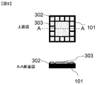
- a structure in which squares are regularly arranged in a lattice shape may be used. As shown in the top view of FIG. 8 and the AA cross-sectional view of the top view, a large square lattice 303 is placed in the middle, and the center is in the middle. A lattice 302 smaller than the large square lattice 303 may be arranged. Further, as a result, if printing can be performed in an area of 70 to 90%, a structure in which the printing is irregularly arranged is also possible.
- the sintered joint is connected to the connecting portion where the semiconductor chip 103 and the heat sink 101 are connected via the sintered metal 102, and the semiconductor chip 103 and the heat sink 101 are sintered. It is composed of a space facing each other without the metal 102. By configuring in this way, it becomes possible to increase the proportion of the space without simply increasing the porosity of the sintered metal, so that the bonding can be performed while maintaining the bonding strength and heat dissipation, and the electronic circuit board 100 It is possible to provide the electronic control device 10 in which the warpage is suppressed.
- the arrangement of the connecting material for joining the copper wiring 105 and the semiconductor chip 103 may be configured in the same pattern as the pattern for applying the sintered metal paste of the heat sink 101 and the semiconductor chip 103.
- the bonding layer on the heat sink 101 side and the copper wiring 105 side of the semiconductor chip 103 can have the same structure, so that the thermal expansion coefficient can be made uniform on both sides of the semiconductor chip 103. It is possible to provide the electronic control device 10 in which the warpage is suppressed.
- a structure in which the lattices are regularly arranged is preferable.
- a large square lattice 303 is placed in the middle as shown in FIG. A structure in which a lattice 302 smaller than the lattice 303 is disposed is preferable.
- the thickness of the bonding material shall be 10um or more and 400um or less. This is because if the thickness is 10 ⁇ m or less, it is difficult to relieve the stress at the joint even with the value of the elastic modulus. Moreover, it is because heat dissipation will worsen in the thickness of 400 um or more.
- the first is a method using metal nanoparticles having an average particle size of 100 nm or less.
- the metal is sintered at a low temperature of 350 ° C. or less.
- Metal nanoparticles can be bonded to, for example, Au or Ag, at the bonding partner electrode during bonding.
- the surface oxide film can be directly reduced and bonded to Cu, Ni, etc., there is an advantage that treatment such as noble metal plating on the Cu heat sink, and hence Ni plating is unnecessary.
- the reason why the counter electrode can be reduced in this manner is that the metal particles are coated with an organic substance in order to maintain stability at room temperature.
- organic substances that coat the metal particles include alkylcarboxylic acids, alkylamines, and alkylthiols. Among these, it is particularly preferable to use alkylcarboxylic acid and alkylamine which are highly reducible with respect to the oxide film.
- the metal particles include two types of silver and copper. Both types of metal have very high heat dissipation. However, considering cost, it is preferable to use copper.
- the second is a method using metal oxide particles of about 100 nm to 10 ⁇ m.
- the metal oxide particles used here include gold oxide, silver oxide, and copper oxide.
- the metal oxide particles have an average particle size of 100 nm to 10 ⁇ m. This is because when the average particle size of the metal oxide is larger than 10 ⁇ m, the dispersibility in the conductive bonding material is deteriorated and it is difficult to obtain a dense bonding layer. Furthermore, when the particle size is larger than this, the screen is clogged when screen printing is performed. The reason why the average particle size is 100 nm or more is that the stability of silver oxide is particularly deteriorated when the average particle size is less than 100 nm.
- reducing agents When metal oxide particles are used, a combination with a reducing agent is essential in order to reduce the metal oxide particles to the metal during bonding.
- a reducing agent one or more mixtures selected from alcohols, carboxylic acids, and amines composed of organic substances having 30 or less carbon atoms can be used. These have not only the effect of reducing the metal oxide particles into metal, but also the effect of improving the dispersibility in the organic solvent by covering the metal particles around the mixed particles with an organic substance.
- the reducing agent when stearic acid is used as the reducing agent, for example, when silver oxide is used as the metal oxide, the silver oxide and the stearic acid adhering to it undergo a reduction reaction at 140 to 150 ° C. Removed from the silver oxide particles. For this reason, if the mixing ratio of silver oxide is too large compared to the amount of stearic acid, the reduction reaction cannot be sufficiently caused and silver oxide remains in the bonding material. This does not increase the bonding strength. Therefore, the reducing agent for silver oxide is 0.1 wt% or more. In addition, if a large amount of stearic acid is present, stearic acid remains after bonding, which causes a decrease in bonding strength, so the limit is 50 wt% or less.
- the reason why the number of carbon atoms in the organic reducing agent is set to 30 or less is that if the number of carbon atoms increases too much, the boiling point of the dispersing agent becomes high, and the dispersing agent remains in the joining portion even when heated (for example, 200 ° C.) during joining. This is because it may remain and cause a problem in bonding strength and reliability.
- Examples of the compound containing an available alcohol group include alkyl alcohols such as ethanol, propanol, butyl alcohol, pentyl alcohol, hexyl alcohol, heptyl alcohol, octyl alcohol, nonyl alcohol, decyl alcohol, undecyl alcohol, There are dodecyl alcohol, tridecyl alcohol, tetradecyl alcohol, pentadecyl alcohol, hexadecyl alcohol, heptadecyl alcohol, octadecyl alcohol, nonadecyl alcohol, and icosyl alcohol.
- alkyl alcohols such as ethanol, propanol, butyl alcohol, pentyl alcohol, hexyl alcohol, heptyl alcohol, octyl alcohol, nonyl alcohol, decyl alcohol, undecyl alcohol
- dodecyl alcohol tridecyl alcohol, tetradecyl alcohol, pentadecyl alcohol
- ethylene glycol triethylene glycol, or a compound having a large number of alcohol groups such as citric acid, ascorbic acid, and glucose may be used.
- alkyl carboxylic acid as a compound containing available carboxylic acid.
- Specific examples include butanoic acid, pentanoic acid, hexanoic acid, heptanoic acid, octanoic acid, nonanoic acid, decanoic acid, undecanoic acid, dodecanoic acid, tridecanoic acid, tetradecanoic acid, pentadecanoic acid, hexadecanoic acid, heptadecanoic acid, octadecanoic acid, Nonadecanoic acid, icosanoic acid and oleic acid can be mentioned.
- a secondary carboxylic acid type, tertiary carboxylic acid type, dicarboxylic acid, and a carboxyl compound having a cyclic structure can be used.
- the reducing material to be used is not limited to the organic substance containing the alcohol and carboxylic acid, and an organic substance containing an aldehyde group, an ester group, a sulfanyl group, a ketone, or an amino group can be used.
- the third is a method using silver particles of about 100 nm to 10 um.
- Metal particles are sintered at a low temperature of 400 ° C. or less even when the particle size is 10 ⁇ m or less, and are used as a bonding material. This is because the silver particles are coated with an organic substance in order to maintain stability at room temperature.
- organic substances that coat the metal particles include alkylcarboxylic acids, alkylamines, and alkylthiols. Among these, it is particularly preferable to use alkylcarboxylic acid and alkylamine which are highly reducible with respect to the oxide film.
- the conductive bonding material used in this embodiment may be generated only with metal oxide particles and a reducing agent (plus other metal particles), but when used as a paste-like bonding material, the boiling point is 350 ° C. or less.
- a solvent examples include alcohols.
- the reason why the boiling point is set to 350 ° C. or lower is that the target for the bonding temperature is 200 to 250 ° C., so that if the boiling point is too high, it takes too much time to evaporate. This is because it is considered appropriate.
- organic substances such as alcohols having boiling points exceeding the temperature are absolutely unsuitable. Of course, such an organic material may be used depending on the application.
- Available organic substances having alcohol groups include methanol, ethanol, propanol, butyl alcohol, pentyl alcohol, hexyl alcohol, heptyl alcohol, octyl alcohol, nonyl alcohol, decyl alcohol, undecyl alcohol, dodecyl alcohol, tridecyl alcohol, tetradecyl There are alcohol, pentadecyl alcohol, hexadecyl alcohol, heptadecyl alcohol, octadecyl alcohol, nonadecyl alcohol, and icosyl alcohol.
- glycols such as diethylene glycol, ethylene glycol, and triethylene glycol can be used.
- terpineol ethylene glycol, triethylene glycol, or a compound having a large number of alcohol groups such as citric acid, ascorbic acid, and glucose may be used.
- a glycol-based solvent it is preferable to use a glycol-based solvent. This is because glycol-based solvents are inexpensive and have little toxicity to human bodies.
- metal particles having an average particle size of 10 ⁇ m or less may be mixed in the bonding material in advance.
- the type of such metal at least one metal selected from platinum, palladium, rhodium, osmium, ruthenium, iron, tin, zinc, cobalt, nickel, chromium, titanium, tantalum, tungsten, indium, silicon, aluminum and the like.
- an alloy made of two or more kinds of metals can be used. These may be mixed and used within a range that does not significantly deteriorate the characteristics of the conductive bonding material in the present invention.
- the organic substance containing the alcohol group not only the organic substance containing the alcohol group but also an organic substance containing a carboxylic acid, an amine, an aldehyde group, an ester group, a sulfanyl group, a ketone group, or the like can be used. Furthermore, you may use the organic substance which does not have the above functional groups, and consists only of toluene or a hydrocarbon, and hexane, a cyclohexane, etc. are mentioned as such an example.
- the organic solvent used in this manner the boiling point may be 350 ° C. or less, and from such a solvent, it is possible to use not only one type but also a mixture of two or more types.
- the amount of the organic solvent to be mixed may be within 50% by weight (more preferably within 20% by weight) when the metal material to be sintered in the present invention is 100% by weight.
- the mixture may be stirred and mixed using a mortar, a grinder, a vibration ball mill, a roller mill, a planetary ball mill or the like.
- ⁇ Joint conditions When the above three kinds of sinterable metal particle materials are used, it is essential to apply heat in order to join them. As joining conditions, it is preferable to apply heating at 100 ° C. or more and 350 ° C. or less within 1 second or more and 180 minutes or less.
- the heating temperature was set to 100 ° C. or more because it is impossible to achieve bonding when the heating is performed at a temperature lower than this.
- the reason for setting the heating time to 180 minutes or less is that if the heating time is set to 180 minutes or more, it takes too much time to produce one product and it is difficult to perform mass production.
- the bonding atmosphere at this time is not limited to the air, but a reducing atmosphere, for example, a hydrogen atmosphere or an inert atmosphere such as a nitrogen atmosphere or an argon atmosphere can be used.
- a reducing atmosphere for example, a hydrogen atmosphere or an inert atmosphere such as a nitrogen atmosphere or an argon atmosphere.
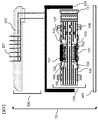
- FIG. 2 is an exploded view showing a state before assembly for explaining a schematic configuration of an engine ECU (Electric Control Unit) of the vehicle in the present embodiment.
- the ECU 10 includes a housing 301, an electronic circuit board 100 accommodated in the housing 301, and a connector portion 200.
- the housing 301 is made of, for example, polybutylene terephthalate (PBT) or the like, one of which is open, and the other is formed with a hole (not shown) for inserting a connector terminal. And the internal space which accommodates the electronic circuit board 100 in this is comprised.
- PBT polybutylene terephthalate
- the substrate unit 111 is composed of a copper wiring 105 and via holes (not shown) for connecting the wirings.
- the electronic circuit board 100 is configured by mounting electronic components such as a heat sink 101, a semiconductor chip (microcomputer) 103, a capacitor 106, and a resistor on the board portion 111.
- a material of the substrate unit 111 for example, a substrate made of epoxy resin and glass fiber is used.
- the electronic circuit board 100 having the above-described configuration is used.
- the present invention is not limited to the above-described configuration, and other resin substrates and ceramic substrates can be applied. Copper is preferable for the heat sink 103 from the viewpoint of heat dissipation, but lighter Al or the like may be used.
- the surface may be used after being subjected to Ni plating, Ag plating, Au plating, or the like.
- the semiconductor chip 103 is a heat generating semiconductor chip 103 that generates excessive heat.
- Reference numeral 103 denotes a semiconductor chip that generates heat as shown in the claims.
- the connector 201 is a connector as an external connection terminal mounted on the electronic circuit board 100, and the connector 201 has one end exposed to the outside of the housing 301 in a state where the housing 301 and the cover 401 are fastened. It is configured.
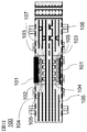
- FIG. 3 is a diagram showing a schematic configuration of the electronic circuit board 100 after assembly. As shown in FIG. 3, the joint between the semiconductor chip 103 and the heat sink 101 is reduced in stress by the pattern structure.
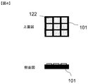
- FIG. 4 is a diagram illustrating a printing method of the sintered metal paste bar 122 before joining the heat sink 101 and the semiconductor chip 103.
- the semiconductor chip 103 and the copper heat sink 101 are first joined.
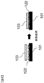
- Fig. 5 shows the joining method.
- the copper heat sink 101 and the semiconductor chip 103 are joined using a sintered metal.
- a sintered metal paste material 122 to be a sintered metal is printed on the copper heat sink 101 using a lattice mask.
- the area to be printed at this time is smaller than the chip size (for example, if the chip size is 8 mm, it is narrower than 8 mm ⁇ 8 mm), but the paste material is printed so that the plane density is 70% or less in that area (for example, When the chip size is 8 mm, 9 squares of 2 mm x 2 mm are evenly arranged at 1 mm intervals).
- the above-mentioned three kinds of metal pastes can be used as the paste that becomes the sintered metal. Next, they are joined by heat treatment as described above. As the atmosphere at this time, a reducing / air / inert atmosphere may be adopted as described above.
- the bonding temperature can also be in the range of 150 to 300 ° C.
- the semiconductor chip 103 is mounted on the copper wiring 105 on the circuit board 100 through the bonding material 104.
- the solder at this time is connected using lead-free solder.
- As the lead-free solder Sn-Cu solder, Sn-Ag-Cu solder, Sn-Ag-Cu-Bi solder, etc. are used, but not limited to these, only contact without using solder such as press-fit connection.
- the circuit board 100 on which the semiconductor chip 103 is mounted which may be electrically connected by soldering, is attached to the housing 301.
- a metal joining technique in which the aforementioned Au, Ag, ⁇ ⁇ Cu, or the like is sintered may be used.
- the thermal expansion coefficients can be made uniform on both sides of the semiconductor chip 103.
- the pattern of the connecting material 104 the same as that of the sintered metal 102, the stress applied to both surfaces of the semiconductor chip 103 can be made uniform, so that it is possible to reduce the warp during use. Become. Also, the stress on both sides of the semiconductor chip 103 can be made uniform by using the same material for the connecting material 104 and the sintered metal 102.
- solder when solder is used as the bonding material 104, the solder is melted and bonded. Therefore, even if the semiconductor chip 103 is slightly warped, the stress generated by the warp is absorbed easily. Therefore, it is preferable in the case where a low-cost semiconductor chip 103 with large chip variation is used as the semiconductor chip 103. Further, with this configuration, even if the semiconductor chip 103 is damaged or the like, the solder on the circuit board 100 side can be easily replaced with another semiconductor chip 103 by remelting the solder. There is a merit that improves.
- the sealing material a thermosetting resin or a thermoplastic resin may be used.
- an electronic control device as shown in FIG. 6 can be obtained.
- FIG. 7 is an exploded view showing a state before assembly for explaining a schematic configuration of an engine ECU (Electric Control Unit) of the vehicle in the present embodiment.
- ECU Electric Control Unit
- the difference between the first embodiment and the present embodiment is that an electronic circuit board 110 having two semiconductor chips 103 exposed from the electronic circuit board is used.
- this electronic circuit board 110 the heat sink 101 bonded to the semiconductor chip 103 installed at the upper part and the lower part is both exposed to the outside of the electronic circuit board 110.
- the inside of the housing 301 and the cover 401 are all sealed with a sealing resin 501 with a resin.
- a structure in which heat is more easily transmitted to the outside than the structure according to the first embodiment is obtained, and warpage can be suppressed by improving heat dissipation.
Landscapes
- Cooling Or The Like Of Semiconductors Or Solid State Devices (AREA)
- Cooling Or The Like Of Electrical Apparatus (AREA)
Abstract
本発明の課題は、耐熱性及び放熱性と低応力を同時に実現した電子回路基板及び電子制御装置を提供することである。本発明に係る電子制御装置は、一方の面に配線用端子を備える半導体チップと、前記配線用端子と第一の接続層を介して接続される配線用端子を有する基板と、前記半導体チップと第二の接続層を介して直接接続されるヒートシンクと、を有する電子制御装置において、前記第二の接続層は、前記半導体チップと前記ヒートシンクとが対向する空間の30~70%の領域が焼結金属で構成されていることを特徴とする電子制御装置。
Description
本発明は、自動車用のエンジンルームに配置される電子制御装置に関する。
従来より、例えば車両の制御に用いられるエンジン制御装置(ECU)には、演算処理を行うマイコン、外部負荷やセンサなどと接続される入出力回路、これらの回路に電源を供給する電源回路などが、基板上に配置されている。当該回路等は、ケース及びカバーからなる筐体に収容されている。
また、従来のエンジン制御装置の実装構造では、制御基板に搭載する電子部品の数の増加に伴い、制御基板が大きくなることから、エンジン制御装置のサイズ増大の要因となっている。近年、車両サイズに対する居住スペース(車内空間)の割合は、快適さを求めるため増加傾向にある。このためエンジン制御装置は車載に設置するためのスペースが限られているため小型化が望まれている。
一方で小型化した場合には、半導体チップの単位面積あたりの発熱量が増加するため、接合部の温度が上昇する傾向にある。従って接合部には耐熱性と放熱性の両方が要求されている。
特許文献1には、基板を小型化する技術の一つに半導体チップ等の電子部品を基板に内蔵する方法が開示されている。当該特許文献1のように電子部品を基板に埋め込むことで、基板サイズを小型化することが可能になる。
しかし、特許文献1に記載の電子部品内蔵型基板では放熱経路が基板と平行な方向のみであるため、半導体チップからの発熱量が増加してくると放熱性が不十分になる。
一方、特許文献2には半導体チップの垂直方向からの放熱性を向上させるために、半導体素子の上面にヒートシンクを配置したものが開示されている。
また、特許文献3には金属ナノ粒子を焼結させて接合する技術が開示されている。
実際の接合プロセスでは基板への熱履歴を減らすためにヒートシンクと半導体チップを接合してから基板に接合するプロセスが採用される。しかしこのようなプロセスでは、特許文献2に記載の発明でさらに放熱性を向上させるために、特許文献3に記載の焼結金属を用いると、これらの焼結金属の弾性率が高いために接合後に半導体チップの反りが発生し、その後の電子基板への接合が極めて困難になるという問題があった。
そこで本発明は、上記の事情に鑑みてなされたものであり、耐熱性及び放熱性と低応力を同時に実現した電子回路基板及び電子制御装置を提供することを課題とする。
本発明に係る電子制御装置は、一方の面に配線用端子を備える半導体チップと、前記配線用端子と第一の接続層を介して接続される配線用端子を有する基板と、前記半導体チップと第二の接続層を介して直接接続されるヒートシンクと、を有する電子制御装置において、前記第二の接続層は、前記半導体チップと前記ヒートシンクとが対向する空間の30~70%の領域が焼結金属で構成されていることを特徴とする電子制御装置。
本発明によれば、耐熱性・放熱性と低応力化を同時に実現できる電子回路基板及び電子制御装置を提供することが可能となる。
この出願の発明は、上記の通りの特徴を持つものであるが、以下にその実施の形態について説明する。
<ヒートシンク101と半導体チップ103の接合構造>
本発明では、ヒートシンク101と半導体チップ103とを接合する焼結金属の接合構造を低密度な構造にすることで応力を緩和し・半導体チップ103の反りを防止することが可能である。具体的な低密度構造としては以下に挙げるものである。
本発明では、ヒートシンク101と半導体チップ103とを接合する焼結金属の接合構造を低密度な構造にすることで応力を緩和し・半導体チップ103の反りを防止することが可能である。具体的な低密度構造としては以下に挙げるものである。
本発明では、反りを抑制するための一つの要因として接合部の密度が重要になる。図1に銀の密度に対する弾性率の関係を示す。バルクの銀の密度は10.5g/cm3である。半導体チップ103とヒートシンク101との間に形成された銀の接合部の密度が7.35g/cm3以下、つまり接合部の密度が銀のバルク密度に対して70%以下のときには、銅からなるヒートシンク101の反りを抑制するために必要な弾性率である30GPa以下となるため好ましい。これは現行使用されているSnAgCuの鉛フリーはんだの弾性率が約30GPaであり、この値になると反りの問題がなくなるためである。また、半導体チップ103とヒートシンク101との間に形成された銀の接合部の密度が3.15g/cm3以上、つまり接合部の密度が銀のバルク密度に対して30%以上のときには接合強度及び放熱性を十分確保することが出来、使用時のヒートシンク101の反りを抑制することが可能となるため好ましい。
したがって、半導体チップ103とヒートシンク101の間に形成された接合部の密度は、半導体チップ103とヒートシンク101との間に形成された接合部が全て銀などの金属で埋められている場合と比較して接合部の金属密度が30%以上70%以下であること、つまり、半導体チップ103とヒートシンク101とが対向して形成される空間の30%~70%の領域が焼結金属で構成されていることが好ましい。なお、ここでは便宜上銀を使用して説明したが、銅などの金属でも同様の金属密度であることが好ましい。
低密度化するには接合面でパターンを形成することで可能となる。これにより接合部の低応力化が可能となる。このような構造としては、ヒートシンク101の上から見た場合に平面状で正方形、長方形、円、三角、ひし形、楕円等の形状にして各種パターンを描くことが可能である。結果として平面内において70~90%の領域を占める程度になればよい。例えば格子状に正方形を規則的に配列させる構造でもよいし、図8の上面図及び当該上面図のA―A断面図に示すように、真ん中に大きな正方形の格子303をおいて、周囲に真ん中の大きな正方形の格子303よりも小さな格子302を配置させてもよい。また、結果的に70~90%の領域で印刷が可能であれば不規則に配置させる構造でも可能である。
焼結金属ペーストのパターンを作成することによって、焼結後の接合部は、半導体チップ103とヒートシンク101とが焼結金属102を介して接続される接続部と、半導体チップ103とヒートシンク101が焼結金属102を介さず対向してなる空間から構成される。このように構成することによって、単純に焼結金属の空隙率を上げすぎることなく空間の割合を増やすことが可能となるため、接合強度及び放熱性を保ちつつ接合ができ、電子回路基板100の反りを抑制した電子制御装置10を提供することが可能となる。
また、銅配線105と半導体チップ103の接合する接続材料の配置を上記ヒートシンク101と半導体チップ103の焼結金属ペーストを塗布するパターンと同様のパターンで構成しても良い。
このように構成することによって、半導体チップ103のヒートシンク101側、及び銅配線105側の接合層を同様の構造とすることができるので半導体チップ103の両面で熱膨張係数を揃えることが可能となり、反りを抑制した電子制御装置10を提供することが可能となる。
なお、このときには半導体チップ103の両面で同じ種類の焼結金属を用いた方が、熱膨張係数を揃えることが可能となるため、より好ましい。
なお、均一に応力を低減するという観点からは、格子状に規則的に配列させる構造が好ましい。また、十分な熱拡散をさせて放熱性を向上させて使用時の応力低減を重視する場合は、図8に示すように真ん中に大きな正方形の格子303をおいて、周囲に真ん中の大きな正方形の格子303よりも小さな格子302を配置させる構造が好ましい。
さらには上記数字の範囲内であれば不規則な形状を不規則に配置させる構造でも結果的に応力を緩和することが可能となる。
上記の接合に用いる焼結金属材料はいずれも高い放熱性を有しているためその密度が低下しても十分な放熱性を有することになる。
また、接合材料の厚さは10um以上400um以下とする。10um以下の厚みでは上記弾性率の値でも接合部の応力を緩和することが困難になるからである。また、400um以上の厚さでは放熱性が悪くなるためである。
以下で本発明で用いる3種類の低温焼結する金属粒子材料について述べる。
<金属ナノ粒子の例>
1つ目は平均粒径が100nm以下の金属ナノ粒子を用いる方法である。粒径が100nm以下になると350℃以下の低温で金属が焼結するようになる。この方法では接合後にはバルクの金属となるため高い放熱性と耐熱性が得られる。金属ナノ粒子は接合時に接合相手電極に例えばAuやAgに対して接合が可能である。また、CuやNiなどに対しても表面酸化膜を還元して直接接合が可能であるためCuのヒートシンクへの貴金属めっき、しいてはNiめっきなどの処理が不要になるメリットがある。このように相手電極を還元することが可能なのは金属粒子が室温での安定性を保つために有機物で被覆されているためである。金属粒子を被覆する有機物としてはアルキルカルボン酸、アルキルアミン、アルキルチオールがある。この中でも特に酸化膜に対して還元性の強いアルキルカルボン酸、アルキルアミンを用いることが好ましい。
1つ目は平均粒径が100nm以下の金属ナノ粒子を用いる方法である。粒径が100nm以下になると350℃以下の低温で金属が焼結するようになる。この方法では接合後にはバルクの金属となるため高い放熱性と耐熱性が得られる。金属ナノ粒子は接合時に接合相手電極に例えばAuやAgに対して接合が可能である。また、CuやNiなどに対しても表面酸化膜を還元して直接接合が可能であるためCuのヒートシンクへの貴金属めっき、しいてはNiめっきなどの処理が不要になるメリットがある。このように相手電極を還元することが可能なのは金属粒子が室温での安定性を保つために有機物で被覆されているためである。金属粒子を被覆する有機物としてはアルキルカルボン酸、アルキルアミン、アルキルチオールがある。この中でも特に酸化膜に対して還元性の強いアルキルカルボン酸、アルキルアミンを用いることが好ましい。
上記金属粒子としては銀、銅の2種類が挙げられる。2種類の金属とも放熱性が非常に高い。が、コストを考えると、銅を用いることが好ましい。
<金属酸化物の例>
2つ目は100nm~10um程度の金属酸化物粒子を用いる方法である。ここで用いる金属酸化物粒子としては酸化金、酸化銀、酸化銅がある。金属酸化物粒子は、平均粒径が100nm以上10um以下としている。金属酸化物の平均粒径が10umより大きくなると、導電性接合材料中における分散性が悪くなり、緻密な接合層を得ることが困難になるためである。さらにこれ以上の粒径になるとスクリーン印刷をする場合はスクリーンに目詰まりをおこしたりするからである。また、平均粒径を100nm以上としたのは、平均粒子が100nm未満になると特に酸化銀の安定性が悪くなるからである。
2つ目は100nm~10um程度の金属酸化物粒子を用いる方法である。ここで用いる金属酸化物粒子としては酸化金、酸化銀、酸化銅がある。金属酸化物粒子は、平均粒径が100nm以上10um以下としている。金属酸化物の平均粒径が10umより大きくなると、導電性接合材料中における分散性が悪くなり、緻密な接合層を得ることが困難になるためである。さらにこれ以上の粒径になるとスクリーン印刷をする場合はスクリーンに目詰まりをおこしたりするからである。また、平均粒径を100nm以上としたのは、平均粒子が100nm未満になると特に酸化銀の安定性が悪くなるからである。
<還元剤の例>
金属酸化物粒子を用いる場合には接合時に還元して金属に戻すため還元剤との組み合わせが必須である。還元剤としては炭素数30以下の有機物からなるアルコール類、カルボン酸類、アミン類から選ばれた1種以上の混合物を用いることができる。これらは金属酸化物粒子を還元して金属にする効果だけではなく、混合粒子の溶媒への金属粒子の周りを有機物で被覆し、有機溶剤への分散性を向上する作用もある。
金属酸化物粒子を用いる場合には接合時に還元して金属に戻すため還元剤との組み合わせが必須である。還元剤としては炭素数30以下の有機物からなるアルコール類、カルボン酸類、アミン類から選ばれた1種以上の混合物を用いることができる。これらは金属酸化物粒子を還元して金属にする効果だけではなく、混合粒子の溶媒への金属粒子の周りを有機物で被覆し、有機溶剤への分散性を向上する作用もある。
ここで、還元剤として例えばステアリン酸を用いた場合、金属酸化物として酸化銀を用いた場合、酸化銀とそれに付着していたステアリン酸とが140~150℃で還元反応を起こし、ステアリン酸が酸化銀粒子から除去される。このため、酸化銀の混合割合がステアリン酸の量に比べて多すぎると、十分に還元反応を起こすことができずに酸化銀が接合材内に残ってしまう。これでは接合強度が上がらない。よって、酸化銀に対する還元剤は0.1wt%以上とする。また、多量にステアリン酸が存在すると接合後にステアリン酸が残存し、接合強度の低下を招くため50wt%以下を限度とする。
有機物還元剤の炭素数を30以下としたのは、炭素数が多くなりすぎると、分散材の沸点が高くなってしまって、接合時に加熱(例えば200℃)しても分散材が接合部分に残ってしまい、接合強度及び信頼性に問題となる可能性があるからである。
また、利用可能なアルコール基を含む化合物としては、アルキルアルコールが挙げられ、例えば、エタノール、プロパノール、ブチルアルコール、ペンチルアルコール、ヘキシルアルコール、ヘプチルアルコール、オクチルアルコール、ノニルアルコール、デシルアルコール、ウンデシルアルコール、ドデシルアルコール、トリデシルアルコール、テトラデシルアルコール、ペンタデシルアルコール、ヘキサデシルアルコール、ヘプタデシルアルコール、オクタデシルアルコール、ノナデシルアルコール、イコシルアルコール、がある。さらには1級アルコール型に限らず、2級アルコール型、3級アルコール型、及びアルカンジオール、環状型の構造を有するアルコール化合物を用いることが可能である。それ以外にも、エチレングリコール、トリエチレングリコール、または、クエン酸、アスコルビン酸、グルコースなど多数のアルコール基を有する化合物を用いてもよい。
また、利用可能なカルボン酸を含む化合物としてアルキルカルボン酸がある。具体例としては、ブタン酸、ペンタン酸、ヘキサン酸、ヘプタン酸、オクタン酸、ノナン酸、デカン酸、ウンデカン酸、ドデカン酸、トリデカン酸、テトラデカン酸、ペンタデカン酸、ヘキサデカン酸、ヘプタデカン酸、オクタデカン酸、ノナデカン酸、イコサン酸、オレイン酸が挙げられる。また、上記アルコール基と同様に1級アルコール型に限らず、2級カルボン酸型、3級カルボン酸型、及びジカルボン酸、環状型の構造を有するカルボキシル化合物を用いることが可能である。
また、用いる還元材は上記アルコール、カルボン酸を含む有機物に限らず、アルデヒド基やエステル基、スルファニル基、ケトン、アミノ基などを含む有機物を用いることが可能である。
<金属粒子の例>
3つ目は100nm~10um程度の銀粒子を用いる方法である。金属粒子は10um以下の粒径でも400℃以下の低温で焼結し、接合材料として用いられる。この銀粒子は室温での安定性を保つために有機物で被覆されているためである。金属粒子を被覆する有機物としてはアルキルカルボン酸、アルキルアミン、アルキルチオールがある。この中でも特に酸化膜に対して還元性の強いアルキルカルボン酸、アルキルアミンを用いることが好ましい。
3つ目は100nm~10um程度の銀粒子を用いる方法である。金属粒子は10um以下の粒径でも400℃以下の低温で焼結し、接合材料として用いられる。この銀粒子は室温での安定性を保つために有機物で被覆されているためである。金属粒子を被覆する有機物としてはアルキルカルボン酸、アルキルアミン、アルキルチオールがある。この中でも特に酸化膜に対して還元性の強いアルキルカルボン酸、アルキルアミンを用いることが好ましい。
<ペースト溶剤>
本実施形態で用いられる導電性接合材料は金属酸化物粒子と還元剤(プラス他の金属粒子)のみで生成してもよいが、ペースト状の接合材料として用いる場合には沸点が350℃以下の溶媒を加えて用いてもよい。このような溶媒としては例えばアルコール類等が挙げられる。ここで、沸点350℃以下としたのは、接合温度のターゲットが200~250℃であるので、あまり沸点が高いと蒸発するのに時間が掛かりすぎるからであり、350℃を限度にするのが適当と考えられるからである。ただし、その温度を超える沸点を有するアルコール類等の有機物が絶対に不適かというとそうではない。用途によってはそのような有機物を用いても良いのはもちろんである。
本実施形態で用いられる導電性接合材料は金属酸化物粒子と還元剤(プラス他の金属粒子)のみで生成してもよいが、ペースト状の接合材料として用いる場合には沸点が350℃以下の溶媒を加えて用いてもよい。このような溶媒としては例えばアルコール類等が挙げられる。ここで、沸点350℃以下としたのは、接合温度のターゲットが200~250℃であるので、あまり沸点が高いと蒸発するのに時間が掛かりすぎるからであり、350℃を限度にするのが適当と考えられるからである。ただし、その温度を超える沸点を有するアルコール類等の有機物が絶対に不適かというとそうではない。用途によってはそのような有機物を用いても良いのはもちろんである。
利用可能なアルコール基を有する有機物としては、メタノール、エタノール、プロパノール、ブチルアルコール、ペンチルアルコール、ヘキシルアルコール、ヘプチルアルコール、オクチルアルコール、ノニルアルコール、デシルルコール、ウンデシルアルコール、ドデシルアルコール、トリデシルアルコール、テトラデシルアルコール、ペンタデシルアルコール、ヘキサデシルアルコール、ヘプタデシルアルコール、オクタデシルアルコール、ノナデシルアルコール、イコシルアルコール、がある。また、ジエチレングリコール、エチレングリコール、トリエチレングリコールなどのグリコール系を用いることができる。さらには1級アルコール型に限らず、2級アルコール型、3級アルコール型、及びアルカンジオール、環状型の構造を有するアルコール化合物を用いることが可能である。それ以外にも、テルピネオール、エチレングリコール、トリエチレングリコール、または、クエン酸、アスコルビン酸、グルコースなど多数のアルコール基を有する化合物を用いてもよい。これらの中でもグリコール系の溶媒を用いることが好ましい。これはグリコール系の溶媒は安価で、人体等に対する毒性も少ないからである。
また、接合材料中には平均粒径が10um以下の金属粒子を予め混合しておいてもよい。このような金属の種類としては白金、パラジウム、ロジウム、オスミウム、ルテニウム、鉄、錫、亜鉛、コバルト、ニッケル、クロム、チタン、タンタル、タングステン、インジウム、ケイ素、アルミニウム等の中から少なくとも1種類の金属あるいは2種類以上の金属からなる合金を用いることが可能である。これらは本発明における導電性接合材料の特性を大きく低下させない範囲で混合させて用いてもよい。
また、上記アルコール基を含む有機物に限らず、カルボン酸、アミン、アルデヒド基やエステル基、スルファニル基、ケトン基などを含む有機物を用いることができる。さらには、上記のような官能基を有さない、トルエンや、炭化水素のみからなる有機物を用いてもよく、そのような例としてはヘキサン、シクロへキサンなどが挙げられる。このように用いる有機溶剤としては沸点が350℃以下であればよく、そのような中からは1種のみではなく、2種類以上の混合物を用いることが可能である。ここで、350℃以下の沸点を有する有機物とは、一般に市販されている、Seiko Instruments 製TG/DTA6200や、島津製作所製TGA-50等の熱重量測定が可能な装置を用いて10℃/min において窒素中において測定を行った場合に350℃までに99wt%の重量減少を起こす有機物とする。
混合する有機溶剤の量は本発明における焼結する金属材料を100重量%とした場合に50重量%以内(より好適には20重量%以内)であればよい。この際には乳鉢、擂潰機、振動ボールミル、ローラーミル、遊星ボールミル等を用いて攪拌して混合すればよい。
<接合条件>
上記の3種類の焼結性金属粒子材料を用いた場合は、接合するためには熱を加えることが必須である。接合条件としては、1秒以上180分以内で100℃以上350℃以下の加熱を加えることが好ましい。
上記の3種類の焼結性金属粒子材料を用いた場合は、接合するためには熱を加えることが必須である。接合条件としては、1秒以上180分以内で100℃以上350℃以下の加熱を加えることが好ましい。
また、接合強度向上のために、必要があれば加圧をかけて用いてもよい。 加熱温度を100℃以上としたのは、これよりも低温での加熱であると、接合を達成することが不可能だからである。
加熱時間を180分以下としたのは加熱時間を180分以上とすると、一つの製品を作製するのにあまりにも多くの時間がかかり、大量生産を行うことが難しくなるからである。
このときの接合雰囲気としては、大気中に限らず、還元雰囲気、例えば、水素雰囲気、または不活性雰囲気である窒素雰囲気、アルゴン雰囲気などを用いることが可能である。このような雰囲気で接合を行うことで、電子部品等の大気中での酸化等の問題を軽減することが可能となる。
以下、具体的な実施形態を用いて本発明をより詳細に説明する。
<第一の実施形態>
図2は、本実施形態における車両のエンジンECU(Electric Control Unit)の概略構成を説明するための組み付け前の状態を示す分解図である。図2に示すように、ECU10は、筐体301、当該筐体301内に収容される電子回路基板100と、コネクタ部分200により構成される。
<第一の実施形態>
図2は、本実施形態における車両のエンジンECU(Electric Control Unit)の概略構成を説明するための組み付け前の状態を示す分解図である。図2に示すように、ECU10は、筐体301、当該筐体301内に収容される電子回路基板100と、コネクタ部分200により構成される。
筐体301は、例えばポリブチレンテレフタラート(PBT)等からなり、一方が開放され、もう片方はコネクタ端子を差し込むための穴(図示しない)が形成された構成となる。
そして、この中に電子回路基板100を収容する内部空間を構成する。
そして、この中に電子回路基板100を収容する内部空間を構成する。
基板部111は、銅配線105や当該配線間を接続するビアホール(図示しない)等から構成されるものである。電子回路基板100は、当該基板部111に、ヒートシンク101、半導体チップ(マイコン)103、コンデンサ106、抵抗等の電子部品を実装して構成されるものである。本実施形態においては、基板部111の材料としては、例えばエポキシ樹脂とガラスファイバーからなる基板を用いている。
なお、本実施形態では上記構成の電子回路基板100を用いたが、上記構成に限定されるものではなく、それ以外の樹脂基板や、セラミック基板を適用することができる。ヒートシンク103には銅が放熱性の観点から好ましいが、より軽いAlなどを用いてもよい。
また、表面にはNiめっき、Agめっき、Auめっき等を施して使用してもよい。
また、表面にはNiめっき、Agめっき、Auめっき等を施して使用してもよい。
また、半導体チップ103が、過度に発熱する発熱する半導体チップ103である。この103が、特許請求の範囲で示す発熱する半導体チップである。尚、コネクタ201は、電子回路基板100に実装された外部接続端子としてのコネクタであり、当該コネクタ201は、筺体301とカバー401を締結した状態で、一端が筐体301外に露出するように構成されている。
次に、半導体チップ103にて生じた熱をヒートシンク101に放出する電子回路基板100の放熱構造の詳細を、図3、図4、及び図5を用いて説明する。図3は、組み付け後の電子回路基板100の概略構成を示す図である。図3に示すように半導体チップ103とヒートシンク101の接合部はパターン構造により低応力化されている。
図4は、ヒートシンク101と半導体チップ103の接合前の焼結金属ペースト 122の印刷方法を示す図である。図4に示すような電子回路基板100の放熱構造を形成するためには、半導体チップ103と銅のヒートシンク101をはじめに接合する。
図5にその接合方法を示す。まず、焼結金属を用いて、銅のヒートシンク101と半導体チップ103を接合する。銅のヒートシンク101上に焼結金属となる焼結金属ペースト材料122を格子マスクを用いて印刷する。この際の印刷する領域はチップサイズよりも小さくが(例えばチップサイズが8mmの場合は8mm×8mmよりも狭い)、その領域において平面の密度70%以下となるようにペースト材料を印刷する(例えばチップサイズが8mmの場合は2mm×2mmの9つの正方形を1mm間隔で均等に配置する)。
また、焼結金属となるペーストは前述した3種類の金属ペーストを用いることが可能である。次にこれらを上述したような熱処理することで接合を行う。この際の雰囲気も前述のように還元・大気・不活性雰囲気などを採用してよい。また、接合温度も150~300℃の範囲で行うことが可能である。
次に図2で示すように、例えば接合材料104を介して半導体チップ103を回路基板100上の銅配線105に実装する。この際のはんだとしては鉛フリーはんだを用いて接続されている。鉛フリーはんだとしては、Sn-Cuはんだ、Sn-Ag-Cuはんだ、Sn-Ag-Cu-Biはんだ等が用いられるが、特にこれらに限らず、プレスフィット接続等のはんだを用いず、接触のみで電気的に接続させる無はんだ接続でもよい、この半導体チップ103が実装された回路基板100を、筐体301に取り付ける。また、前述したAu, Ag, Cuなどを焼結させた金属接合技術を用いてもよい。
なお、半導体チップ103の熱応力を低減するという観点を重視すると接合材料104に焼結金属を用いる方が、半導体チップ103の両面で熱膨張係数を揃えることが可能になるので好ましい。この際には、接続材料104のパターンを焼結金属102と同様のパターンにすることによって、半導体チップ103の両面にかかる応力を揃えることが出来るため、使用時により反りを低減することが可能となる。また、接続材料104と焼結金属102を同様の材料とすることによっても半導体チップ103の両面に係る応力を揃えることが可能となる。
一方で、接合材料104にはんだを用いた場合には、はんだが融解して接合されるため、仮に半導体チップ103に若干の反りがあったとしても、はんだで反りによって発生する応力を無理なく吸収することが出来るため、半導体チップ103にチップばらつきの大きい低価格な半導体チップ103を用いる場合では好ましい。また、このように構成することによって、仮に半導体チップ103が破損等したとしても、回路基板100側のはんだを再度溶融させることによって、別の半導体チップ103と容易に交換可能になるため、生産性が向上するというメリットがある。
また図2や図3にも示すように、封止樹脂107で、電子回路基板100の半導体チップ103及び銅のヒートシンク101を封止するのが望ましい。これによりヒートシンク101と半導体チップ103の接合部の信頼性が向上する。また、樹脂107で封止することで半導体チップ103からの放熱性も向上する。この封止材料としては熱硬化性樹脂、あるいは熱可塑性樹脂を用いてよい。
このような工程を得て図6に示すような電子制御装置を得ることが出来る。
<第二の実施形態>
図7は、本実施形態における車両のエンジンECU(Electric Control Unit)の概略構成を説明するための組み付け前の状態を示す分解図である。
図7は、本実施形態における車両のエンジンECU(Electric Control Unit)の概略構成を説明するための組み付け前の状態を示す分解図である。
第一の実施形態と本実施形態で異なる点は、2つの半導体チップ103がそれぞれ電子回路基板から露出された構成となる電子回路基板110を用いた点である。この電子回路基板110は上部と下部に設置した半導体チップ103に接合されたヒートシンク101がどちらも電子回路基板110外部に露出されている。このような構造にすることによって、電子回路基板110のコネクタ200側に配置されているヒートシンク101までの構成と、電子回路基板110のカバー401側に配置されているヒートシンク101までの構成を同様にすることが可能となる。
したがって、電子回路基板110の上下で熱膨張係数を揃えることが可能となり、電子制御装置20を使用している最中に、熱による電子回路基板110の反りを抑制することができる。
また、筺体301とカバー401の内部が全て樹脂で封止樹脂501により封止されている。このような構造により第一の実施形態に係る構造よりもより外部へ熱が伝わりやすい構造となり放熱性の向上により反りを抑制することが可能となる。
以上、本発明の実施形態について詳述したが、本発明は、前記実施形態に限定されるものではなく、特許請求の範囲に記載された本発明の精神を逸脱しない範囲で、種々の設計変更を行なうことができるものである。例えば、前記した実施形態は本発明をわかりやすく説明するために詳細に記載したものであり、必ずしも説明した全ての構成を備えるものに限定されるものではない。また、ある実施形態の構成の一部を他の実施形態の構成に置き換えることが可能であり、また、ある実施形態の構成に他の実施形態の構成を加えることも可能である。さらに、各実施形態の構成の一部について、他の構成の追加・削除・置換をすることが可能である。
10,20 電子制御装置(ECU)
100 電子回路基板
101 ヒートシンク
102 焼結金属
103 半導体チップ
104 接合材料
105 銅配線
106 コンデンサ
107 封止樹脂
111 基板部
110 電子回路基板
200 コネクタ
201 コネクタ端子
202 コネクタカバー
301 筺体
401 カバー
501 封止樹脂
100 電子回路基板
101 ヒートシンク
102 焼結金属
103 半導体チップ
104 接合材料
105 銅配線
106 コンデンサ
107 封止樹脂
111 基板部
110 電子回路基板
200 コネクタ
201 コネクタ端子
202 コネクタカバー
301 筺体
401 カバー
501 封止樹脂
Claims (10)
- 一方の面に配線用端子を備える半導体チップと、
前記配線用端子と第一の接続層を介して接続される配線用端子を有する基板と、
前記半導体チップと第二の接続層を介して直接接続されるヒートシンクと、を有する電子制御装置において、
前記第二の接続層は、前記半導体チップと前記ヒートシンクとが対向する空間の30~70%の領域が焼結金属で構成されていることを特徴とする電子制御装置。 - 請求項1に記載の電子制御装置において、
前記第二の接続層は、前記半導体チップと前記ヒートシンクが焼結金属を介して接続される接続部と、前記半導体チップと前記ヒートシンクが前記前記焼結金属を介さず対向している空間からなることを特徴とする電子制御装置。 - 請求項2に記載の電子制御装置において、
前記第一の接続層は、前記半導体チップと前記配線用端子が接続材料を介して接続される接続部と、前記半導体チップと前記配線用端子が接続材料を介さずに対向している空間からなることを特徴とする電子制御装置。 - 請求項3に記載の電子制御装置において、前記第二の接続層の空間は前記焼結金属が格子状になるように形成されることを特徴とする電子制御装置。
- 請求項4に記載の電子制御装置において、前記第二の接続層の前記半導体チップ中央部領域に設けられた格子状の焼結金属の方が、当該中央部領域の周囲に設けられた格子状の焼結金属よりも大きい事を特徴とする電子制御装置。
- 請求項3乃至5のいずれかに記載の電子制御装置において、
前記第一の接続層の接続材料ははんだで構成されることを特徴とする電子制御装置。 - 請求項3乃至5のいずれかに記載の電子制御装置において、
前記第一の接続層の接続材料は焼結金属であることを特徴とする電子制御装置。 - 請求項3乃至5のいずれかに記載の電子制御装置において、
前記第一の接続層を構成する接続材料は、前記第二の接続層を構成する焼結金属と同様の配置となるように設けられていることを特徴とする電子制御装置。 - 請求項8に記載の電子制御装置において、前記焼結金属は金粒子、銀粒子、酸化銀粒子、銅粒子、酸化銅粒子のいずれかを用いて形成されていることを特徴とする電子制御装置。
- 請求項1乃至9のいずれかに記載の電子制御装置において、
前記半導体チップ、前記ヒートシンク、及び前記配線用端子が封止樹脂で封止されていることを特徴とする電子制御装置。
Applications Claiming Priority (2)
| Application Number | Priority Date | Filing Date | Title |
|---|---|---|---|
| JP2012-188204 | 2012-08-29 | ||
| JP2012188204A JP6014419B2 (ja) | 2012-08-29 | 2012-08-29 | 電子制御装置 |
Publications (1)
| Publication Number | Publication Date |
|---|---|
| WO2014034306A1 true WO2014034306A1 (ja) | 2014-03-06 |
Family
ID=50183126
Family Applications (1)
| Application Number | Title | Priority Date | Filing Date |
|---|---|---|---|
| PCT/JP2013/069335 Ceased WO2014034306A1 (ja) | 2012-08-29 | 2013-07-17 | 電子制御装置 |
Country Status (2)
| Country | Link |
|---|---|
| JP (1) | JP6014419B2 (ja) |
| WO (1) | WO2014034306A1 (ja) |
Cited By (1)
| Publication number | Priority date | Publication date | Assignee | Title |
|---|---|---|---|---|
| WO2019088285A1 (ja) * | 2017-11-06 | 2019-05-09 | 三菱マテリアル株式会社 | ヒートシンク付パワーモジュール用基板およびヒートシンク付パワーモジュール用基板の製造方法 |
Families Citing this family (4)
| Publication number | Priority date | Publication date | Assignee | Title |
|---|---|---|---|---|
| JP6927490B2 (ja) * | 2017-05-31 | 2021-09-01 | 株式会社応用ナノ粒子研究所 | 放熱構造体 |
| JP2026063984A (ja) * | 2024-10-01 | 2026-04-13 | デクセリアルズ株式会社 | 熱伝導シート、及び熱伝導シートの製造方法 |
| JP2026063983A (ja) * | 2024-10-01 | 2026-04-13 | デクセリアルズ株式会社 | 熱伝導シート、及び熱伝導シートの製造方法 |
| JP2026063982A (ja) * | 2024-10-01 | 2026-04-13 | デクセリアルズ株式会社 | 熱伝導シート、及び熱伝導シートの製造方法 |
Citations (5)
| Publication number | Priority date | Publication date | Assignee | Title |
|---|---|---|---|---|
| JPH01106451A (ja) * | 1987-10-20 | 1989-04-24 | Hitachi Ltd | 半導体装置 |
| JPH01117049A (ja) * | 1987-10-30 | 1989-05-09 | Hitachi Ltd | 集積回路素子冷却装置 |
| JPH02246141A (ja) * | 1989-03-17 | 1990-10-01 | Fujitsu Ltd | 半導体装置 |
| JP2003529934A (ja) * | 2000-03-31 | 2003-10-07 | シーメンス アクチエンゲゼルシヤフト | 2つのワークピース間の熱伝導可能な結合部の形成のための方法 |
| JP2009094341A (ja) * | 2007-10-10 | 2009-04-30 | Renesas Technology Corp | 半導体装置、半導体装置の製造方法および接続材料 |
Family Cites Families (10)
| Publication number | Priority date | Publication date | Assignee | Title |
|---|---|---|---|---|
| JPS5752142A (en) * | 1980-07-23 | 1982-03-27 | Hitachi Ltd | Bonding method for pellet |
| JPS63181436A (ja) * | 1987-01-23 | 1988-07-26 | Matsushita Electronics Corp | 回路装置 |
| KR20000015941A (ko) * | 1997-03-24 | 2000-03-15 | 야스카와 히데아키 | 반도체 장치 및 그 제조 방법 |
| JP4770379B2 (ja) * | 2005-10-13 | 2011-09-14 | 富士電機株式会社 | 金属部材の接合方法およびその組立治具 |
| JP4895994B2 (ja) * | 2006-12-28 | 2012-03-14 | 株式会社日立製作所 | 金属粒子を用いた接合方法及び接合材料 |
| JP4950693B2 (ja) * | 2007-02-19 | 2012-06-13 | 株式会社フジクラ | 電子部品内蔵型配線基板及びその実装部品 |
| JP4870223B1 (ja) * | 2010-09-02 | 2012-02-08 | ニホンハンダ株式会社 | ペースト状銀粒子組成物、金属製部材接合体の製造方法および金属製部材接合体 |
| JP5613253B2 (ja) * | 2010-10-08 | 2014-10-22 | 田中貴金属工業株式会社 | 半導体素子接合用の貴金属ペースト |
| JP6146007B2 (ja) * | 2012-03-30 | 2017-06-14 | 三菱マテリアル株式会社 | 接合体の製造方法、パワーモジュールの製造方法、パワーモジュール用基板及びパワーモジュール |
| JP2014029897A (ja) * | 2012-07-31 | 2014-02-13 | Hitachi Ltd | 導電性接合体およびそれを用いた半導体装置 |
-
2012
- 2012-08-29 JP JP2012188204A patent/JP6014419B2/ja not_active Expired - Fee Related
-
2013
- 2013-07-17 WO PCT/JP2013/069335 patent/WO2014034306A1/ja not_active Ceased
Patent Citations (5)
| Publication number | Priority date | Publication date | Assignee | Title |
|---|---|---|---|---|
| JPH01106451A (ja) * | 1987-10-20 | 1989-04-24 | Hitachi Ltd | 半導体装置 |
| JPH01117049A (ja) * | 1987-10-30 | 1989-05-09 | Hitachi Ltd | 集積回路素子冷却装置 |
| JPH02246141A (ja) * | 1989-03-17 | 1990-10-01 | Fujitsu Ltd | 半導体装置 |
| JP2003529934A (ja) * | 2000-03-31 | 2003-10-07 | シーメンス アクチエンゲゼルシヤフト | 2つのワークピース間の熱伝導可能な結合部の形成のための方法 |
| JP2009094341A (ja) * | 2007-10-10 | 2009-04-30 | Renesas Technology Corp | 半導体装置、半導体装置の製造方法および接続材料 |
Cited By (4)
| Publication number | Priority date | Publication date | Assignee | Title |
|---|---|---|---|---|
| WO2019088285A1 (ja) * | 2017-11-06 | 2019-05-09 | 三菱マテリアル株式会社 | ヒートシンク付パワーモジュール用基板およびヒートシンク付パワーモジュール用基板の製造方法 |
| JP2019087607A (ja) * | 2017-11-06 | 2019-06-06 | 三菱マテリアル株式会社 | ヒートシンク付パワーモジュール用基板およびヒートシンク付パワーモジュール用基板の製造方法 |
| US11257735B2 (en) | 2017-11-06 | 2022-02-22 | Mitsubishi Materials Corporation | Heat sink-equipped power module substrate and manufacturing method for heat sink-equipped power module substrate |
| JP7043794B2 (ja) | 2017-11-06 | 2022-03-30 | 三菱マテリアル株式会社 | ヒートシンク付パワーモジュール用基板およびヒートシンク付パワーモジュール用基板の製造方法 |
Also Published As
| Publication number | Publication date |
|---|---|
| JP6014419B2 (ja) | 2016-10-25 |
| JP2014045156A (ja) | 2014-03-13 |
Similar Documents
| Publication | Publication Date | Title |
|---|---|---|
| JP5286115B2 (ja) | 半導体装置及び接合材料 | |
| KR101157742B1 (ko) | 도전성 접합 재료, 그것을 이용한 접합 방법, 및 그것에 의하여 접합된 반도체 장치 | |
| JP4895994B2 (ja) | 金属粒子を用いた接合方法及び接合材料 | |
| JP5151150B2 (ja) | 導電性焼結層形成用組成物、これを用いた導電性被膜形成法および接合法 | |
| JP5006081B2 (ja) | 半導体装置、その製造方法、複合金属体及びその製造方法 | |
| JP4848674B2 (ja) | 樹脂金属複合導電材料およびその製造方法 | |
| US8592996B2 (en) | Semiconductor device and method of manufacturing the same | |
| JP5525335B2 (ja) | 焼結銀ペースト材料及び半導体チップ接合方法 | |
| CN103515343B (zh) | 电子元器件模块及其制造方法 | |
| JP5023710B2 (ja) | 半導体装置及びその製造方法 | |
| EP3041042B1 (en) | Method of producing bonded body and method of producing power module substrate | |
| JP7551497B2 (ja) | 電子部品及び電子部品の製造方法 | |
| JP6014419B2 (ja) | 電子制御装置 | |
| JP2014029897A (ja) | 導電性接合体およびそれを用いた半導体装置 | |
| JPWO2007122925A1 (ja) | 電子部品、それを用いた電子部品装置およびその製造方法 | |
| JP2012191238A (ja) | 導電性焼結層形成用組成物、これを用いた導電性被膜形成法および接合法 | |
| TW201618627A (zh) | 用於產生焊接連接之方法 | |
| JP2012038790A (ja) | 電子部材ならびに電子部品とその製造方法 | |
| JP5677685B2 (ja) | 回路基板、及びそれを用いた半導体装置 | |
| JP4624222B2 (ja) | 導電部形成用粒子 | |
| WO2018074188A1 (ja) | インダクタ部品、インダクタ部品の製造方法 | |
| JP2007158291A (ja) | 電気製品、その製造方法、及びその方法に用いる接合材料 |
Legal Events
| Date | Code | Title | Description |
|---|---|---|---|
| 121 | Ep: the epo has been informed by wipo that ep was designated in this application |
Ref document number: 13833446 Country of ref document: EP Kind code of ref document: A1 |
|
| NENP | Non-entry into the national phase |
Ref country code: DE |
|
| 122 | Ep: pct application non-entry in european phase |
Ref document number: 13833446 Country of ref document: EP Kind code of ref document: A1 |