WO2014034014A1 - 情報取得装置および物体検出装置 - Google Patents
情報取得装置および物体検出装置 Download PDFInfo
- Publication number
- WO2014034014A1 WO2014034014A1 PCT/JP2013/004475 JP2013004475W WO2014034014A1 WO 2014034014 A1 WO2014034014 A1 WO 2014034014A1 JP 2013004475 W JP2013004475 W JP 2013004475W WO 2014034014 A1 WO2014034014 A1 WO 2014034014A1
- Authority
- WO
- WIPO (PCT)
- Prior art keywords
- laser light
- light source
- laser
- information acquisition
- holder
- Prior art date
- Legal status (The legal status is an assumption and is not a legal conclusion. Google has not performed a legal analysis and makes no representation as to the accuracy of the status listed.)
- Ceased
Links
Images







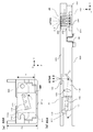
Classifications
-
- G—PHYSICS
- G01—MEASURING; TESTING
- G01B—MEASURING LENGTH, THICKNESS OR SIMILAR LINEAR DIMENSIONS; MEASURING ANGLES; MEASURING AREAS; MEASURING IRREGULARITIES OF SURFACES OR CONTOURS
- G01B11/00—Measuring arrangements characterised by the use of optical techniques
- G01B11/24—Measuring arrangements characterised by the use of optical techniques for measuring contours or curvatures
- G01B11/25—Measuring arrangements characterised by the use of optical techniques for measuring contours or curvatures by projecting a pattern, e.g. one or more lines, moiré fringes on the object
- G01B11/2513—Measuring arrangements characterised by the use of optical techniques for measuring contours or curvatures by projecting a pattern, e.g. one or more lines, moiré fringes on the object with several lines being projected in more than one direction, e.g. grids, patterns
-
- G—PHYSICS
- G01—MEASURING; TESTING
- G01S—RADIO DIRECTION-FINDING; RADIO NAVIGATION; DETERMINING DISTANCE OR VELOCITY BY USE OF RADIO WAVES; LOCATING OR PRESENCE-DETECTING BY USE OF THE REFLECTION OR RERADIATION OF RADIO WAVES; ANALOGOUS ARRANGEMENTS USING OTHER WAVES
- G01S7/00—Details of systems according to groups G01S13/00, G01S15/00, G01S17/00
- G01S7/48—Details of systems according to groups G01S13/00, G01S15/00, G01S17/00 of systems according to group G01S17/00
- G01S7/481—Constructional features, e.g. arrangements of optical elements
-
- G—PHYSICS
- G01—MEASURING; TESTING
- G01V—GEOPHYSICS; GRAVITATIONAL MEASUREMENTS; DETECTING MASSES OR OBJECTS; TAGS
- G01V8/00—Prospecting or detecting by optical means
- G01V8/10—Detecting, e.g. by using light barriers
- G01V8/20—Detecting, e.g. by using light barriers using multiple transmitters or receivers
-
- G—PHYSICS
- G02—OPTICS
- G02B—OPTICAL ELEMENTS, SYSTEMS OR APPARATUS
- G02B7/00—Mountings, adjusting means, or light-tight connections, for optical elements
- G02B7/28—Systems for automatic generation of focusing signals
- G02B7/30—Systems for automatic generation of focusing signals using parallactic triangle with a base line
- G02B7/32—Systems for automatic generation of focusing signals using parallactic triangle with a base line using active means, e.g. light emitter
-
- H—ELECTRICITY
- H03—ELECTRONIC CIRCUITRY
- H03K—PULSE TECHNIQUE
- H03K17/00—Electronic switching or gating, i.e. not by contact-making and –breaking
- H03K17/94—Electronic switching or gating, i.e. not by contact-making and –breaking characterised by the way in which the control signals are generated
- H03K17/941—Electronic switching or gating, i.e. not by contact-making and –breaking characterised by the way in which the control signals are generated using an optical detector
-
- G—PHYSICS
- G01—MEASURING; TESTING
- G01S—RADIO DIRECTION-FINDING; RADIO NAVIGATION; DETERMINING DISTANCE OR VELOCITY BY USE OF RADIO WAVES; LOCATING OR PRESENCE-DETECTING BY USE OF THE REFLECTION OR RERADIATION OF RADIO WAVES; ANALOGOUS ARRANGEMENTS USING OTHER WAVES
- G01S17/00—Systems using the reflection or reradiation of electromagnetic waves other than radio waves, e.g. lidar systems
- G01S17/02—Systems using the reflection of electromagnetic waves other than radio waves
- G01S17/06—Systems determining position data of a target
- G01S17/46—Indirect determination of position data
- G01S17/48—Active triangulation systems, i.e. using the transmission and reflection of electromagnetic waves other than radio waves
-
- H—ELECTRICITY
- H03—ELECTRONIC CIRCUITRY
- H03K—PULSE TECHNIQUE
- H03K2217/00—Indexing scheme related to electronic switching or gating, i.e. not by contact-making or -breaking covered by H03K17/00
- H03K2217/94—Indexing scheme related to electronic switching or gating, i.e. not by contact-making or -breaking covered by H03K17/00 characterised by the way in which the control signal is generated
- H03K2217/941—Indexing scheme related to electronic switching or gating, i.e. not by contact-making or -breaking covered by H03K17/00 characterised by the way in which the control signal is generated using an optical detector
- H03K2217/94102—Indexing scheme related to electronic switching or gating, i.e. not by contact-making or -breaking covered by H03K17/00 characterised by the way in which the control signal is generated using an optical detector characterised by the type of activation
- H03K2217/94108—Indexing scheme related to electronic switching or gating, i.e. not by contact-making or -breaking covered by H03K17/00 characterised by the way in which the control signal is generated using an optical detector characterised by the type of activation making use of reflection
Definitions
- the present invention relates to an object detection apparatus that detects an object in a target area based on a state of reflected light when light is projected onto the target area, and an information acquisition apparatus suitable for use in the object detection apparatus.
- An object detection apparatus using a so-called distance image sensor as an information acquisition apparatus can detect not only a planar image on a two-dimensional plane but also the shape and movement of the detection target object in the depth direction.
- light in a predetermined wavelength band is projected from a laser light source or LED (Light-Emitting-Diode) onto a target area, and the reflected light is received by a light-receiving element such as a CMOS image sensor.
- reflected light from the target area of laser light having a dot pattern is received by a light receiving element. Based on the light receiving position of the dot on the light receiving element, the distance to each part of the detection target object (irradiation position of each dot on the detection target object) is detected using triangulation (for example, non-patent) Reference 1).
- a CAN package type semiconductor laser is used as a laser light source.
- the apparatus in order to save space, the apparatus is required to be thin in the projection direction of the laser beam with respect to the target area.
- a configuration in which the output optical axis of the laser light source is bent by a mirror or the like and the laser light is projected onto the target area can be used.
- a CAN package type semiconductor laser it is necessary to secure an arrangement space corresponding to the diameter of the CAN, and it is difficult to effectively reduce the thickness of the information acquisition device.
- the present invention has been made in view of this point, and provides an information acquisition device and an object detection device capable of effectively reducing the thickness of the device.
- the first aspect of the present invention relates to an information acquisition device.
- An information acquisition apparatus includes: a projection unit that projects a laser beam of a dot pattern onto a target region; a light receiving unit that images the target region; and a base on which the projection unit and the light receiving unit are arranged side by side.
- the projection unit includes a frame package type laser light source, a collimator lens that converts the laser light emitted from the laser light source into parallel light, a mirror that reflects the laser light transmitted through the collimator lens, A diffractive optical element that converts the laser light reflected by the mirror into laser light having a predetermined dot pattern in the target area and projects the laser light on the target area.
- the laser light source, the collimator lens, and the diffractive optical element are installed on the base so that the laser light source, the collimator lens, and the mirror are arranged in a straight line and the diffractive optical element faces a target region. Is done. Further, the laser light source is arranged on the base so that one surface in the thickness direction of the frame constituting the laser light source faces the surface of the base.
- the second aspect of the present invention relates to an object detection apparatus.
- the object detection apparatus according to this aspect includes the information acquisition apparatus according to the first aspect.
- an information acquisition device and an object detection device capable of effectively reducing the thickness of the device.
- the present invention is applied to an information acquisition apparatus of a type that irradiates a target area with laser light having a predetermined dot pattern.
- the projection unit 100 corresponds to a “projection unit” described in the claims.
- the opening 111a corresponds to the “accommodating portion” described in the claims.
- the notch 111b corresponds to an “open portion” described in the claims.
- the step portions 111c, 111d, and 111f correspond to “wall surfaces” recited in the claims.
- the opening 111g corresponds to an “opening portion” described in the claims.
- the groove 111 i corresponds to a “groove” described in the claims.
- the inclined surfaces 111m and 111n correspond to “inclined surfaces” recited in the claims.
- the wall surfaces 111o and 111p correspond to “wall surfaces” recited in the claims.
- the convex portion 112a corresponds to a “contact portion” described in the claims.
- the mountain folded portion 112d corresponds to a “deformed portion” described in the claims.
- the DOE 140 corresponds to a “diffractive optical element” recited in the claims.
- the light receiving unit 200 corresponds to a “light receiving unit” recited in the claims.
- the projection housing portion 410 corresponds to “a structure for mounting the laser light source, the collimator lens, and the mirror” recited in the claims.
- the opening 411a corresponds to an “opening” described in the claims.
- the description of the correspondence between the above claims and the present embodiment is merely an example, and the invention according to the claims is not limited to the present embodiment.
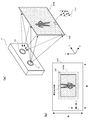
- FIG. 1 shows a schematic configuration of an object detection apparatus 1 according to the present embodiment.
- the object detection device 1 includes an information acquisition device 2 and an information processing device 3.
- the television 4 is controlled by a signal from the information processing device 3.
- the information acquisition device 2 projects infrared light over the entire target area, and receives the reflected light with a CMOS image sensor, whereby the distance between each part of the object in the target area (hereinafter referred to as “three-dimensional distance information”). To get.
- the acquired three-dimensional distance information is sent to the information processing apparatus 3 via the cable 5.
- the information processing device 3 is, for example, a controller for TV control, a game machine, a personal computer, or the like.
- the information processing device 3 detects an object in the target area based on the three-dimensional distance information received from the information acquisition device 2, and controls the television 4 based on the detection result.
- the information processing apparatus 3 detects a person based on the received three-dimensional distance information and detects the movement of the person from the change in the three-dimensional distance information.
- the information processing device 3 is a television control controller
- the information processing device 3 detects the person's gesture from the received three-dimensional distance information and outputs a control signal to the television 4 in accordance with the gesture.
- the application program to be installed is installed.
- the information processing device 3 when the information processing device 3 is a game machine, the information processing device 3 detects the person's movement from the received three-dimensional distance information, and displays a character on the television screen according to the detected movement. An application program that operates and changes the game battle situation is installed.
- FIG. 2 is a diagram showing the configuration of the information acquisition device 2 and the information processing device 3.
- the information acquisition device 2 includes a projection optical system 10 and a light receiving optical system 20 as a configuration of an optical unit.
- the projection optical system 10 and the light receiving optical system 20 are arranged in the information acquisition device 2 so as to be aligned in the X-axis direction.
- the projection optical system 10 includes a laser light source 110, a collimator lens 120, a mirror 130, and a diffractive optical element (DOE: Diffractive Optical Element) 140.
- the light receiving optical system 20 includes an aperture 210, an imaging lens 220, a filter 230, and a CMOS image sensor 240.
- the information acquisition device 2 includes a CPU (Central Processing Unit) 21, a laser driving circuit 22, an imaging signal processing circuit 23, an input / output circuit 24, and a memory 25 as a circuit unit.
- CPU Central Processing Unit
- the laser light source 110 outputs a laser beam having a narrow wavelength band with a wavelength of about 830 nm in a direction approaching the light receiving optical system 20 (X-axis positive direction).
- the collimator lens 120 converts the laser light emitted from the laser light source 110 into substantially parallel light.
- the mirror 130 reflects the laser light incident from the collimator lens 120 side in the direction toward the DOE 140 (Z-axis direction).
- the DOE 140 has a diffraction pattern on the incident surface. Due to the diffractive action of this diffraction pattern, the laser light incident on the DOE 140 is converted into laser light having a predetermined dot pattern and irradiated onto the target area.
- the diffraction pattern of the DOE 140 has, for example, a structure in which a step type diffraction hologram is formed in a predetermined pattern.
- the diffraction hologram is adjusted in pattern and pitch so as to convert the laser light that has been made substantially parallel light by the collimator lens 120 into a laser light having a dot pattern.
- the DOE 140 irradiates the target region with the laser beam incident from the mirror 130 as a laser beam having a dot pattern that spreads radially.
- the laser light reflected from the target area enters the imaging lens 220 through the aperture 210.
- the aperture 210 stops the light from the outside so as to match the F number of the imaging lens 220.
- the imaging lens 220 collects the light incident through the aperture 210 on the CMOS image sensor 240.
- the filter 230 is a band-pass filter that transmits light in the infrared wavelength band including the emission wavelength (about 830 nm) of the laser light source 110 and cuts the wavelength band of visible light.
- the CMOS image sensor 240 receives the light collected by the imaging lens 220 and outputs a signal (charge) corresponding to the amount of received light to the imaging signal processing circuit 23 for each pixel.
- the output speed of the signal is increased so that the signal (charge) of the pixel can be output to the imaging signal processing circuit 23 with high response from the light reception in each pixel.
- the CPU 21 controls each unit according to a control program stored in the memory 25. With this control program, the CPU 21 is provided with the functions of a laser control unit 21a for controlling the laser light source 110 and a distance acquisition unit 21b for generating three-dimensional distance information.
- the laser drive circuit 22 drives the laser light source 110 according to a control signal from the CPU 21.
- the imaging signal processing circuit 23 controls the CMOS image sensor 240, and sequentially captures the signal (charge) of each pixel generated by the CMOS image sensor 240 for each line at a predetermined imaging interval. Then, the captured signals are sequentially output to the CPU 21. Based on the signal (imaging signal) supplied from the imaging signal processing circuit 23, the CPU 21 calculates the distance from the information acquisition device 2 to each part of the detection target by processing by the distance acquisition unit 21b.
- the input / output circuit 24 controls data communication with the information processing device 3.
- the information processing apparatus 3 includes a CPU 31, an input / output circuit 32, and a memory 33.
- the information processing device 3 is configured to communicate with the television 4 and to read information stored in an external memory such as a CD-ROM and install it in the memory 33.
- an external memory such as a CD-ROM
- the configuration of these peripheral circuits is not shown for the sake of convenience.
- the CPU 31 controls each unit according to a control program (application program) stored in the memory 33.
- a control program application program
- the CPU 31 is provided with the functions of an object detection unit 31a for detecting an object in the image and a function control unit 31b for controlling the function of the television 4 according to the movement of the object.
- Such a control program is read from a CD-ROM by a drive device (not shown) and installed in the memory 33, for example.
- the object detection unit 31a extracts the shape of the object in the image from the three-dimensional distance information supplied from the information acquisition device 2, and detects the movement of the extracted object shape.
- the function control unit 31b executes a predetermined process according to the detection result by the object detection unit 31a. For example, when the control program is a game program, the function control unit 31b executes a process for operating a character on the television screen in accordance with a human movement (gesture) detected by the object detection unit 31a.
- the control program is a program for controlling the function of the television 4
- the function control unit 31 b performs the function (channel switching) of the television 4 based on a signal from the object detection unit 31 a according to a person's movement (gesture). And volume adjustment, etc.) are executed.
- the input / output circuit 32 controls data communication with the information acquisition device 2.
- the projection optical system 10 and the light receiving optical system 20 are installed side by side with a predetermined distance in the X axis direction so that the projection center of the projection optical system 10 and the imaging center of the light receiving optical system 20 are aligned on a straight line parallel to the X axis. Is done.
- FIG. 3A is a diagram schematically showing the irradiation state of the laser light on the target region
- FIG. 3B is a diagram schematically showing the light receiving state of the laser light in the CMOS image sensor 240.
- FIG. 3B shows a flat surface (screen) in the target area and a light receiving state when a person is present in front of the screen.
- the projection optical system 10 irradiates the target area with laser light having a dot pattern (hereinafter, the entire laser light having this pattern is referred to as “DP light”).
- DP light the entire laser light having this pattern
- the light flux region of DP light is indicated by a solid line frame.
- dot regions hereinafter simply referred to as “dots” generated by the diffraction action by the DOE 140 are scattered according to the dot pattern by the diffraction action by the DOE 140.
- the DP light reflected thereby is distributed on the CMOS image sensor 240 as shown in FIG.
- the entire DP light receiving area on the CMOS image sensor 240 is indicated by a broken line frame, and the DP light receiving area incident on the imaging effective area of the CMOS image sensor 240 is indicated by a solid line frame.
- the light of Dt0 on the target area shown in FIG. 3A enters the position of Dt0 ′ shown in FIG. 3B on the CMOS image sensor 240.
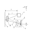
- FIG. 4 is a diagram for explaining a distance detection method according to the present embodiment.
- a flat reflection plane RS perpendicular to the Z-axis direction is disposed at a predetermined distance Ls from the projection optical system 10.
- the emitted DP light is reflected by the reflection plane RS and enters the CMOS image sensor 240 of the light receiving optical system 20.
- an electrical signal for each pixel in the effective imaging area is output from the CMOS image sensor 240.
- the output electric signal value (pixel value) for each pixel is developed on the memory 25 of FIG.
- reflection image an image composed of all pixel values obtained by reflection from the reflection plane RS
- reflection plane RS is referred to as a “reference plane”.
- the DP light (DPn) corresponding to the region Sn on the reference image is reflected by the object, and is in a region Sn ′ different from the region Sn.
- the projection optical system 10 and the light receiving optical system 20 are adjacent to each other in the X-axis direction, the displacement direction of the region Sn ′ with respect to the region Sn is parallel to the X-axis.
- the region Sn ′ is displaced in the positive direction of the X axis with respect to the region Sn. If the object is at a position farther than the distance Ls, the region Sn ′ is displaced in the negative X-axis direction with respect to the region Sn.
- the distance Lr from the projection optical system 10 to the portion of the object irradiated with DP light (DPn) is triangulated using the distance Ls. Calculated based on Similarly, the distance from the projection optical system 10 is calculated for the part of the object corresponding to another region.
- Non-Patent Document 1 The 19th Annual Conference of the Robotics Society of Japan (September 18-20, 2001) Proceedings, P1279-1280).
- FIG. 5 is an exploded perspective view showing the configuration of the information acquisition apparatus 2 according to the present embodiment.
- the information acquisition device 2 includes a projection unit 100, a light receiving unit 200, a circuit board 300, and a base 400.
- the CPU 21, the laser drive circuit 22, the input / output circuit 24, and the memory 25 shown in FIG. 2 are arranged on the circuit board 300, and the imaging signal processing circuit 23 is arranged on the image sensor circuit board 241.
- the projection unit 100 includes a laser holder 111, a collimator lens holder 121, and a pressing spring 122 in addition to the projection optical system 10 (laser light sources 110 to DOE 140) shown in FIG.
- the laser holder 111 holds the laser light source 110
- the collimator lens holder 121 holds the collimator lens 120
- the holding spring 122 is used to mount the collimator lens holder 121 on the base 400.
- the light receiving unit 200 includes a lens barrel 250, an imaging lens holder 260, and an image sensor circuit board 241 in addition to the above-described light receiving optical system 20 (aperture 210 to CMOS image sensor 240).
- the lens barrel 250 holds the aperture 210 and the imaging lens 220, and the imaging lens holder 260 holds the lens barrel 250 and the filter 230.
- a CMOS image sensor 240 is installed on the image sensor circuit board 241.
- the image sensor circuit board 241 is connected to the circuit board 300 by the FPC 301.
- FIG. 5 shows the aperture 210 among the aperture 210 and the imaging lens 220 held in the lens barrel 250.
- the filter 230 is attached to the surface on the negative side of the Z-axis of the imaging lens holder 260.
- Projection unit 100 is installed on the surface of base 400 on the negative side of the Z-axis.
- the aperture 210, the imaging lens 220, and the filter 230 are installed on the surface on the negative side of the Z-axis of the base 400 via the lens barrel 250 and the imaging lens holder 260.
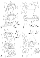
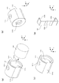
- FIG. 6A is an exploded perspective view of the laser light source 110 and the laser holder 111.
- FIG. 6B is a perspective view showing the structure in a state where the laser light source 110 and the laser holder 111 are assembled.
- the X-axis positive direction is the forward direction
- the Y-axis positive direction is the left direction
- the Z-axis positive direction is the upward direction.
- the laser light source 110 is attached to the laser holder 111 by a leaf spring 112.
- a jig mounting member 113 is mounted on the laser holder 111.
- the jig mounting member 113 is used when adjusting the position of the laser light source 110. That is, when the position of the laser light source 110 is adjusted with respect to the base 400, a jig for position adjustment is mounted on the jig mounting member 113.
- FIG. 7A is a perspective view of the laser light source 110 and the leaf spring 112 viewed from the Z axis positive side (upper side)
- FIG. 7B is a perspective view of the laser light source 110 and the leaf spring 112 on the Z axis negative side (lower side).
- FIG. 7C is a perspective view of the laser holder 111 and the jig mounting member 113 as viewed from the Z axis positive side (upper side)
- FIG. 7D shows the laser holder 111 and the jig mounting member 113 in the Z axis negative direction. It is the perspective view seen from the side (lower side).
- the laser light source 110 is a frame package type semiconductor laser.
- the laser light source 110 includes a frame 110a, a mold 110b, a laser element 110c, and three terminals 110d.
- the frame 110a has a flat shape in the Z-axis direction.
- the frame 110a is made of metal or the like having excellent thermal conductivity in order to dissipate heat generated by the laser element 110c.
- a mold 110b is formed on the frame 110a.
- the mold 110b is a resin frame member opened in the positive direction of the X axis.
- the laser element 110c is disposed at a central position surrounded by the mold 110b on the frame 110a.
- the laser element 110c is electrically connected to the three terminals 110d by wires or the like. Each terminal 110 d is electrically connected to the laser drive circuit 22 mounted on the circuit board 300.
- a central portion on the front side of the frame 110a is formed with a protrusion 110e protruding forward in a comb shape.
- the left end front surface portion 110f and the right end front surface portion 110g of the frame 110a are each a plane parallel to the YZ plane.
- a step portion 110h is formed on the right side surface of the frame 110a, and the right side surface of the step portion 110h is a plane parallel to the XZ plane.
- the boundary between the right end front surface portion 110g and the step portion 110h is a smooth curved surface with chamfered corners.
- the lower surface 110i of the frame 110a is a plane parallel to the XY plane.
- the frame 110a is formed with two flange portions 110j and 110k symmetrically on the outside of the mold 110b.
- the upper surfaces of the two flange portions 110j and 110k are planes parallel to the XY plane.
- the step 110h is formed on the side edge of the flange 110k.
- the leaf spring 112 is a spring-like plate-like member, and has a shape in which the front end portion and the left and right end portions are bent downward as shown in the figure.
- convex portions 112a and 112b projecting downward are formed on the left and right edges of the leaf spring 112.
- the tips of the convex portions 112a and 112b are each arcuate.
- An opening 112c is provided at the center of the leaf spring 112, and a mountain fold 112d is formed so as to protrude obliquely upward from the front edge of the opening 112c.
- the cross section of the XZ plane has an arc shape at the top of the mountain folded portion 112d.
- a flange 112e bent in a hook shape is formed in the center of the rear end of the leaf spring 112.
- the laser holder 111 is a substantially cubic holding member.
- the laser holder 111 is made of a metal (zinc, magnesium, etc.) having excellent thermal conductivity in order to dissipate heat generated by the laser light source 110.
- the laser holder 111 has an opening 111 a in the center for accommodating the laser light source 110 and the leaf spring 112. Further, a notch 111 b following the opening 111 a is formed on the left side surface of the laser holder 111 so as to follow the shape of the laser light source 110.
- the opening 111a of the laser holder 111 has an upper left-right width smaller than a lower left-right width. Further, the width in the left-right direction of the upper portion of the opening 111a is slightly larger than the width in the left-right direction of the leaf spring 112, and the width in the left-right direction of the lower portion of the opening 111a is slightly larger than the width in the left-right direction of the laser light source 110. It has become.
- Step portions 111c and 111d and a circular opening 111e continuing to the outside are formed on the inner side surface in front of the opening 111a.
- the rear side surfaces of the step portions 111c and 111d are planes parallel to the YZ plane.
- a stepped portion 111f and a rectangular opening 111g extending to the outside are formed on the inner side surface on the right side of the opening 111a.
- the left side surface of the step portion 111f is a plane parallel to the XZ plane.
- the bottom surface of the opening 111a is a flat portion 111h parallel to the XY plane, and a groove 111i for injecting heat gel is formed following the flat portion 111h.
- a groove 111 j that engages with the flange 112 e of the leaf spring 112 is formed on the upper surface of the laser holder 111.
- grooves 111k for mounting the jig mounting member 113 are formed on the lower and right side surfaces of the laser holder 111.
- the front side surface of the laser holder 111 is a flat portion 111l parallel to the YZ plane.
- the jig mounting member 113 has a shape that sandwiches the laser holder 111 from side to side and fits into the groove 111k. As shown in FIG. 7C, the jig mounting member 113 is formed with an L-shaped step 113a. The jig mounting member 113 has a reduced thickness in the front-rear direction due to the formation of the step 113a. The jig mounting member 113 is mounted on the laser holder 111 by fitting the portion of the jig mounting member 113 where the step 113 a is formed into the groove 111 k of the laser holder 111.
- the laser light source 110 when the laser light source 110 is mounted on the laser holder 111, the laser light source 110 and the leaf spring 112 are viewed from the rear with the leaf spring 112 superimposed on the laser light source 110. It is inserted into the opening 111 a of the laser holder 111. The laser light source 110 is pushed forward until the movement is restricted by the inner surface of the opening 111a. Further, the leaf spring 112 is pushed forward until the flange 112e is engaged with the groove 111j of the laser holder 111.
- the mountain fold 112d of the leaf spring 112 is pressed by the inner surface above the opening 111a to bend downward, and the bottom surface of the laser light source 110 is pressed against the flat portion 111h of the opening 111a by the restoring force of the mountain fold 112d. .
- the configuration in which the laser light source 110 is pressed against the flat portion 111h of the opening 111a by the leaf spring 112 is an example of the configuration according to claim 6.
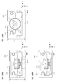
- FIG. 8A and 8B are cross-sectional views showing how the laser light source 110 is attached to the laser holder 111.
- FIG. 7A and 7B are sectional views when the laser light source 110 and the laser holder 111 shown in FIG. 6A are cut along the A-A ′ plane.
- the wall surfaces 111o and 111p are planes parallel to the XZ plane, and the distance between the wall surfaces 111o and 111p is slightly larger than the lateral width of the protrusion 110e.
- the position of the laser light source 110 in the front-rear direction is determined by the left end front surface portion 110f and the right end front surface portion 110g contacting the step portions 111c and 111d of the laser holder 111, respectively. Is done. Further, in the laser light source 110, the protrusion 110e fits between the wall surfaces 111o and 111p of the laser holder 111, and the stepped portion 110h abuts on the stepped portion 111f on the inner side surface of the laser holder 111 in the X axis positive direction. Thus, the position in the left-right direction is determined. Thereby, the emission part of the laser element 110 c of the laser light source 110 is positioned at the center of the opening 111 e of the laser holder 111.
- the left side surface of the laser holder 111 is provided with a notch 111b, so that the left end front portion 110f of the laser light source 110 can be seen by looking inside through the notch 111b. It can be easily confirmed whether the laser holder 111 is in contact with the stepped portion 111c. Further, since the opening 111g is provided on the right side surface of the laser holder 111, the right end front surface portion 110g of the laser light source 110 is formed on the step portion 111d of the laser holder 111 by looking inside through the opening 111g. It can be easily confirmed whether or not they are in contact.
- the configuration in which the notch 111b and the opening 111g are provided in order to confirm the mounting state of the laser light source 110 with respect to the laser holder 111 is an example of the configuration according to claim 8.
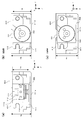
- FIGS. 9A to 9D are views showing a state in which the laser light source 110 and the leaf spring 112 are completely inserted into the opening 111a of the laser holder 111.
- FIG. 9A and 9B are perspective views of the laser holder 111 viewed from the left side and the right side, respectively.
- FIGS. 9C and 9D are views of the laser holder 111 viewed from the left side and the right side, respectively.
- the laser light source 110 is arranged so that the convex portions 112a and 112b of the leaf spring 112 abut on the upper surfaces of the flange portions 110j and 110k, respectively.
- the position is determined. That is, as described above, the upper surface of the flange portions 110j and 110k of the laser light source 110 is pushed downward by the convex portions 112a and 112b of the leaf spring 112 by the restoring force of the elastically deformed mountain fold portion 112d, and the laser The lower surface 110i of the light source 110 is pressed against the flat portion 111h of the opening 111a. As a result, the laser light source 110 is positioned in the vertical direction.
- the adhesive is applied to the boundary portion between the laser light source 110 and the laser holder 111, and the laser light source 110 is connected to the laser holder.
- the adhesive is fixed to 111.
- the heat gel flows into the groove 111 i of the laser holder 111, and the gap between the laser light source 110 and the laser holder 111 is filled.
- the heat generated by the laser element 110c of the laser light source 110 is efficiently transmitted to the laser holder 111 via the frame 110a.
- the configuration in which the groove 111 i is provided in the laser holder 111 in order to apply the heat gel in the gap between the laser light source 110 and the laser holder 111 is an example of the configuration according to claim 9.
- the jig mounting member 113 is fitted into the groove 111k of the laser holder 111 from the lower side, and the jig mounting member 113 is mounted on the laser holder 111. Thereby, as shown in FIG.6 (b), the assembly of the laser light source 110 and the laser holder 111 is completed.
- FIG. 10A is an exploded perspective view of the collimator lens 120 and the collimator lens holder 121.
- FIGS. 10B and 10C are perspective views showing a state in which the collimator lens 120 is mounted on the collimator lens holder 121.
- FIG. 10D is a perspective view showing the holding spring 122.
- the collimator lens holder 121 is a bottomed cylindrical frame member having a substantially circular outline in a front view and having an opening 121a.
- an opening 121b having a diameter smaller than that of the opening 121a is formed at the center of the side surface on the X-axis negative side of the collimator lens holder 121.
- the opening 121 b is for guiding the laser beam to the mirror 130.
- two holes 121c and 121d for allowing an adhesive to flow when the collimator lens 120 and the collimator lens holder 121 are bonded and fixed are formed to be aligned in the Y-axis direction.
- flat portions 121e and 121f parallel to the XY plane are formed symmetrically in the Z-axis direction.
- the diameter of the opening 121a is slightly larger than the diameter of the collimator lens 120.
- the collimator lens 120 is fitted into the opening 121a from the positive side of the X axis until the surface in the negative direction of the X axis of the collimator lens 120 contacts the bottom of the opening 121a (see FIG. 10C). In this state, the adhesive flows into the holes 121c and 121d, and the collimator lens 120 is bonded and fixed to the collimator lens holder 121.
- the holding spring 122 is a leaf spring having a spring property, and has a step 122a one step lower in the center.
- the holding spring 122 has a symmetrical shape in the Y-axis direction.
- the holding spring 122 is formed with two flanges 122 b for mounting the holding spring 122 to the base 400.
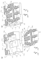
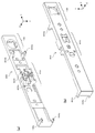
- FIG. 11A is a perspective view of the base 400 viewed from the Z-axis negative side
- FIG. 11B is a perspective view of the base 400 viewed from the Z-axis positive side.
- the base 400 has a plate-like shape that is long in the X-axis direction, and includes a projection housing portion 410 for housing the projection unit 100, and the light receiving unit 200.
- the light receiving housing part 420 for housing the battery is integrally formed.
- the base 400 is made of a metal having high thermal conductivity such as zinc or magnesium.
- the base 400 is formed with convex portions 400a to 400d for mounting the circuit board 300, and further, screw holes 400e and 400f for screwing the circuit board 300 are formed.
- the projection unit 100 and the light receiving unit 200 are mounted on the base 400 so that they are aligned in the X-axis direction.
- the base 400 functions as a heat sink that radiates heat generated by the laser light source 110 and the like to the outside.
- the surface on the negative side of the Z-axis of the projection housing part 410 (the installation surface of the optical member) is one step lower in the positive direction of the Z-axis than the light-receiving housing part 420.
- FIG. 12A is a perspective view of the periphery of the projection housing 410 viewed from the Z-axis negative side.
- FIG. 12B is a perspective view of the periphery of the projection housing 410 viewed from the Y axis positive side.
- FIG. 12C is a perspective view of the periphery of the projection housing 410 viewed from the Z axis positive side.
- the projection housing 410 has a structure for mounting the laser holder 111, the collimator lens holder 121, and the mirror 130 on the surface on the negative side of the Z-axis.
- the projection housing 410 includes a step 411 that is one step lower in the Z-axis positive direction, a wall portion 412 that protrudes in the Z-axis negative direction, a collimator lens holder mounting portion 413, and a mirror mounting portion 414.
- the projection housing unit 410 has a configuration in which a structure for mounting the laser holder 111, the collimator lens holder 121, and the mirror 130 is provided on the surface on the negative side of the Z-axis. It is an example.
- a circular opening 411a is formed at the center of the step portion 411, and square holes 411b and 411c are formed at two corners.
- the wall portion 412 is a plane parallel to the YZ plane, and a U-shaped notch 412a is formed at the center.
- the width in the Y-axis direction of the notch 412a is wider than the width in the Y-axis direction of the opening 111e of the laser holder 111 (see FIG. 7D), and the flat portion 111l of the laser holder 111 (see FIG. 7D). Narrower than the width in the Y-axis direction.
- the height from the step portion 411 to the upper end (end portion in the Z-axis negative direction) of the wall portion 412 is slightly larger than the width of the laser holder 111 in the Z-axis direction. Further, the width of the step portion 411 in the Y-axis direction is considerably wider than the width of the laser holder 111 in the Y-axis direction.
- the structure which provides the step part 411 in the projection housing part 410 of the base 400 is an example of the structure of Claim 4.
- the collimator lens holder mounting portion 413 has a bottom surface 413a parallel to the XY plane, and an inclination inclined from the XY plane by a predetermined angle in the in-plane direction of the YZ plane and in the negative Z-axis direction. Surfaces 413b and 413c are formed. A substantially rectangular opening 413d is formed at the center of the bottom surface 413a.
- a pressing spring mounting portion 413e for mounting the pressing spring 122 is formed in the Y-axis positive / negative direction of the collimator lens holder mounting portion 413.
- the holding spring mounting portion 413e is provided with an engaging portion that engages with the flange 122b of the holding spring 122 to prevent the holding spring 122 from coming off.
- the mirror mounting portion 414 is composed of two inclined surfaces inclined by 45 ° from the XY plane in the in-plane direction of the XZ plane and in the negative Z-axis direction.
- the width in the Y-axis direction between the two inclined surfaces is narrower than the width of the mirror 130 in the Y-axis direction.
- the mirror 130 is tilted by restricting the displacement of the mirror 130 in the X-axis positive direction at a position away from the end in the Z-axis positive direction by a predetermined distance from the end of the mirror mounting portion 414 in the X-axis positive direction.
- Two convex portions 414a for fixing with are formed.
- a DOE mounting portion 415 is formed on the front surface (Z-axis positive direction) of the projection housing portion 410.
- the DOE mounting portion 415 has a contour that allows the DOE 140 to be fitted with a slight gap, and has a flat bottom surface 415 a that is one step lower than the surface of the base 400.
- the depth in the Z-axis direction of the bottom surface 415a is slightly deeper than the thickness of the DOE 140.
- the bottom surface 415a is a plane parallel to the XY plane.
- the DOE mounting portion 415 is formed with wall surfaces 415b to 415e that face the outer periphery of the DOE 140 with a slight gap.
- the wall surfaces 415b and 415d are planes parallel to the XZ plane, and the wall surfaces 415c and 415e are planes parallel to the YZ plane.
- An opening 415f for guiding laser light from the laser light source 110 to the DOE 140 is formed in the center of the bottom surface 415a of the DOE mounting portion 415. Further, substantially U-shaped bonding grooves 415g to 415j for applying an adhesive when the DOE 140 is bonded to the base 400 are formed at the four corners of the DOE mounting portion 415.
- the mirror 130 when assembling the projection unit 100, the mirror 130 is first placed on the mirror mounting portion 414. At this time, the end on the positive side of the Z axis of the mirror 130 is pressed against the two convex portions 414a. In this state, the mirror 130 is bonded and fixed. As a result, the mirror 130 is mounted on the projection housing 410 so as to have an inclination of 45 ° in the in-plane direction of the YZ plane with respect to the XY plane.
- the collimator lens holder 121 to which the collimator lens 120 is attached is placed on the inclined surfaces 413b and 413c.
- the flat portion 121f (see FIG. 10B) of the collimator lens holder 121 does not contact the bottom surface 413a of the collimator lens holder mounting portion 413, and the circumferential portion of the collimator lens holder 121 and the inclined surfaces 413b and 413c. Are in line contact with each other.
- the holding spring 122 is attached to the holding spring mounting portion 413e of the collimator lens holder 121.
- the stepped portion 122a of the holding spring 122 bends in the negative Z-axis direction, and the flat portion 121e of the collimator lens holder 121 is pressed in the positive Z-axis direction by the restoring force.
- the collimator lens holder 121 is pressed against the inclined surfaces 413b and 413c, and the movement in the Y-axis direction and the Z-axis direction is suppressed.
- a jig is attached to the laser holder 111 on which the laser light source 110 is mounted, and the flat portion 111l (see FIG. 7B) on the outer surface of the laser holder 111 in the positive direction of the X axis is the X axis of the wall portion 412. Pressed against the negative side.
- FIG. 13A is a perspective view showing a state in which the laser holder 111 is pressed against the wall 412 by a jig.
- the illustration of the position adjusting jig is omitted.
- a predetermined gap exists between the laser holder 111 and the step portion 411 in the Z-axis direction and the Y-axis direction.
- the laser holder 111 is displaced in the in-plane direction of the YZ plane while being pressed against the wall portion 412 by a jig.
- the position of the laser light source 110 in the in-plane direction of the YZ plane is adjusted so that the optical axis of the laser light source 110 and the optical axis of the collimator lens 120 coincide with each other while the laser light source 110 is displaced. This adjustment is performed with the laser light turned on.
- the position of the collimator lens 120 is adjusted.
- the X-axis of the collimator lens 120 is used so that the collimator lens holder 121 is displaced in the X-axis direction using a jig so that the focal position of the collimator lens 120 is an appropriate position with respect to the light emission point of the laser light source 110.
- Direction adjustment is performed.
- This configuration is an example of the configuration described in claim 2.
- the configuration in which the laser light source 110 is installed on the base 400 via the laser holder 111 in this way is an example of the configuration according to claim 3.
- both the frame 110a and the laser holder 111 of the laser light source 110 are made of metal, and the gap between the frame 110a and the laser holder 111 is filled with the heat gel. Therefore, the heat generated by the laser light source 110 is efficiently transmitted to the base 400 via the laser holder 111 and the heat gel. Thus, the transmitted heat of the laser light source 110 is efficiently radiated to the outside by the base 400 having a large surface area.
- the configuration in which the heat gel is applied through the opening 411a is an example of the configuration according to claim 5.
- an adhesive is evenly applied to the left and right at positions where the collimator lens holder 121 and the inclined surfaces 413b and 413c of the collimator lens holder mounting portion 413 come into contact with each other through the opening 413d. Thereby, the collimator lens holder 121 is bonded and fixed to the projection housing portion 410.
- the DOE 140 is fitted into the DOE mounting portion 415. Since the bottom surface 415a of the DOE mounting portion 415 is a plane parallel to the XY plane, the position of the DOE 140 in the Z-axis direction with respect to the projection housing portion 410 is determined by installing the DOE 140 on the bottom surface 415a of the DOE mounting portion 415. Is done. Further, the side surface on the Y axis positive side and the side surface in the X axis negative direction of the DOE 140 are pressed against the wall surfaces 415b and 415c, respectively, and the positions of the DOE 140 in the Y axis direction and the X axis direction are determined. In this state, the adhesive flows into the adhesive grooves 415g to 415j, and the DOE 140 is fixed to the projection housing part 410.
- the imaging lens holder 260 (see FIG. 5) is attached to the light receiving housing portion 420 (see FIGS. 11A and 11B) of the base 400. As shown in FIGS. 11A and 11B, the light receiving housing 420 has an opening into which the lens barrel 250 (see FIG. 5) is fitted.
- the imaging lens holder 260 is attached to the surface on the negative side of the Z-axis of the light receiving housing portion 420 so that the lens barrel 250 is fitted into the opening (see FIG. 5).
- the image sensor circuit board 241 is attached to the surface on the negative side of the Z-axis of the imaging lens holder 260.
- a recess (not shown) for accommodating the CMOS image sensor 240 is provided on the surface on the negative side of the Z-axis of the imaging lens holder 260.
- the CMOS image sensor 240 is accommodated in the recess.
- the circuit board 300 is fixed to the Z-axis negative side surface of the base 400 by screws 401 and 402.
- notches 300a to 300d (see FIG. 5) formed at the four corners engage with the convex portions 400a to 400d (see FIG. 11A) of the base 400, and the surface on the Z axis positive side Is superimposed on the base 400 from the negative side of the Z-axis so as to contact the upper surface of the wall between the convex portions 400a and 400c and the upper surface of the projection housing portion 410 (see FIG. 11A).
- the screws 401 and 402 are screwed into the screw holes 400e and 400f via the screw grooves 300e and 300f (see FIG. 5), and the circuit board 300 is mounted on the base 400.
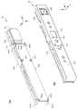
- FIG. 14A is a perspective view of the information acquisition device 2 with the circuit board 300 mounted on the base 400 as viewed from the Z-axis negative side, and FIG. 14B shows the information acquisition device 2 with the Z-axis positive. It is the perspective view seen from the side.
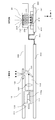
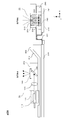
- FIG. 15 is a schematic diagram showing the configuration of the projection optical system 10 and the light receiving optical system 20 of the information acquisition apparatus 2 according to the present embodiment.
- the outgoing optical axis is parallel to the X axis, and the Z axis positive side surface of frame 110 a is parallel to the Z axis negative side surface of base 400. It is installed to become.
- Laser light emitted from the laser light source 110 is converted into substantially parallel light by the collimator lens 120. Then, the laser light transmitted through the collimator lens 120 is reflected in the positive direction of the Z axis by the mirror 130 and enters the DOE 140.
- the laser light source 110, the collimator lens 120, and the mirror 130 of the projection optical system 10 are arranged along the surface of the base 400.
- the height can be reduced.
- the laser light source 110 is configured by a frame package type semiconductor laser
- the height in the Z-axis direction of the information acquisition device 2 can be further reduced as follows.
- the step part 411 is formed in the position of the laser holder 111 of the base 400, the height of the information acquisition apparatus 2 in the Z-axis direction can be further reduced as follows.
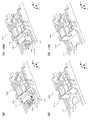
- FIGS. 16A and 16B are perspective views showing the configurations of the laser light source 110 and the base 400 according to the present embodiment, respectively.
- FIGS. 16C and 16D are perspective views showing configurations of a laser light source 160 and a base 400 according to a comparative example, respectively.
- a frame package type semiconductor laser is used as the laser light source 110.
- a step portion 411 is provided, and a circular opening 411a is formed in the step portion 411.
- the opening 411a is used for applying a heat gel. For this reason, the diameter of the opening 411a is smaller than the width of the laser holder 111 in the X-axis direction and the width in the Y-axis direction.
- a CAN package type semiconductor laser is used as the laser light source 160 in the comparative example shown in FIG.
- the CAN package type semiconductor laser has a shape in which a laser element is arranged on a base having a substantially circular outline, and the laser element is covered with a circular CAN slightly smaller than the base.
- the laser light source 160 has a larger dimension in the Z-axis direction than the frame package type laser light source 110.
- a rectangular opening 411d larger than the width of the laser holder 161 in the X-axis direction and the Y-axis direction is formed in the step portion 411 of the base 400.
- the laser holder 161 is configured to fit into the opening 411d.
- FIG. 17A is a schematic diagram of a main part of the configuration of FIG. 16A viewed in the X-axis positive direction
- FIG. 17B is a schematic view of the configuration of FIG. 16B viewed in the X-axis positive direction.
- the dimension ha of laser holder 111 in the Z-axis direction is kept small. Can do.
- a CAN package type semiconductor laser is used for laser light source 160. Therefore, the dimension hb of laser holder 161 in the Z-axis direction is the dimension in the present embodiment. It becomes larger than ha.
- the X-axis direction and the Y-axis of the laser holder 161 are placed on the step 411 as described above.
- An opening 411d larger than the width in the direction is provided, and it is necessary to let the laser holder 161 escape from the opening 411d in the positive direction of the Z axis.
- the laser holder 161 is positioned on the step portion 411, and the heat radiation gel is applied to the gap between the step portion 411 and the laser holder 161. Can take.
- this causes a problem that the height Hc of the base 400 in the Z-axis direction increases and the thickness of the information acquisition device 2 increases.
- the information acquisition apparatus 2 can be thinned while improving the heat dissipation characteristics.
- the optical axis of the laser light source 110 is bent by the mirror 130, the size of the projection optical system 10 is reduced in the projection direction (Z-axis direction) of the laser light with respect to the target region.
- the information acquisition device 2 can be thinned.
- a thin frame package type semiconductor laser is used as the laser light source 110, and the surface on the Z-axis positive side of the frame 110 a of the semiconductor laser passes through the laser holder 111 on the surface (step portion 411). Since the laser light source 110 is installed so as to face the surface of the information acquisition device 2, the information acquisition device 2 can be further thinned.
- the information acquisition device 2 can be further reduced in thickness.
- the opening 411a for allowing the heat gel to flow is formed in the step portion 411 of the base 400, the gap between the base 400 and the laser holder 111 can be easily filled with the heat gel. . Therefore, the heat generated by the laser light source 110 can be efficiently transmitted to the base 400 via the laser holder 111. Thereby, the heat of the laser light source 110 can be efficiently radiated to the outside.
- the laser light source 110 is pressed against the laser holder 111 by the leaf spring 112, the movement of the laser light source 110 in the Z-axis direction is suppressed, and the laser light source 110 is attached to the laser holder 111. Can be performed smoothly.
- the notch 111b is formed on the side surface of the laser holder 111, the inside of the laser holder 111 can be seen through the notch 111b, and the laser light source 110 is attached to the laser holder 111. Can be carried out smoothly and appropriately.
- the opening 111g is formed on the side surface of the laser holder 111, the inside of the laser holder 111 can be seen through the opening 111g, and the mounting work of the laser light source 110 on the laser holder 111 can be performed. It can be performed smoothly and appropriately.
- the laser holder 111 is provided with the groove 111i for allowing the heat gel to flow in, so that the gap between the laser light source 110 and the laser holder 111 can be easily filled. Therefore, heat generated by the laser light source 110 can be efficiently transferred to the laser holder 111.
- the step portion 411 is formed on the base 400, but the step portion 411 may not be formed as shown in FIG.
- the height Hd of the base 400 is thicker than the height Ha of the base 400 in the above embodiment, as shown in FIG. 18B, the CAN package type laser light source 160 is used.
- the base 400 can be configured to be smaller than the height He.
- coating a heat gel was formed in the step part 411 of the base 400, as shown in FIG.18 (c), even if the opening 411a is not formed. good.
- there is another means for applying the heat gel between the laser holder 111 and the step portion 411 such as applying a heat gel to the step portion 411 in advance before mounting the laser holder 111 on the base 400. It should be used.
- the projection housing part 410 for installing the projection optical system 10 is formed on the surface opposite to the target area of the base 400 (Z-axis negative side).
- the projection housing part 410 may be formed on the surface of the base 400 on the target region side (Z-axis positive side), and the projection optical system 10 may be installed.
- the information acquisition device 2 can be thinned by using a thin frame package type semiconductor laser as the laser light source 110.
- a step 403 is provided near the center of the base 400 in order to align the exit pupil of the projection optical system 10 and the entrance pupil of the light receiving optical system 20.
- the light receiving optical system 20 may also be installed on the target area side (Z axis positive side) surface of the base 400 without providing the step 403.
- the laser light source 110 is arranged so that the frame 110 a is parallel to the surface of the base 400.
- the laser light source 110 has one surface in the thickness direction of the frame 110 a on the surface of the base 400.
- the frame 110a is disposed so as to be inclined at a predetermined angle in the in-plane direction of the YZ plane from a position parallel to the surface of the base 400, as shown in FIG. Also good.
- the laser light source 110 may be inclined by a predetermined angle in the in-plane direction of the XZ plane.
- the frame 110a of the laser light source 110 is arranged so as to be parallel to the surface of the base 400 because the thickness of the base 400 can be minimized.
- the laser light source 110, the collimator lens 120, and the mirror 130 are arranged in a straight line, and the DOE 140 faces the target area.
- the configuration in which the laser light source 110, the collimator lens 120, and the DOE 140 are disposed is an example of a configuration according to claim 11.
- the configuration including the circuit board 300 that is electrically connected to the projection unit 10 and the light receiving unit 20 and arranged substantially in parallel with the direction in which the laser light source 110, the collimator lens 120, and the mirror 130 are arranged in a straight line It is an example of the structure of Claim 12.
- the laser holder 111 and the jig mounting member 113 are configured as separate members.
- a jig adjusting hole may be directly formed in the laser holder 111.
- the projection housing part 410 is formed integrally with the base 400, but may be constituted by another member.
- the dimension of the information acquisition device 2 in the Z-axis direction can be more effectively suppressed when the projection housing part 410 is formed integrally with the base 400 as in the above embodiment.
- the filter 230 is disposed to remove light in a wavelength band other than the wavelength band of the laser light irradiated to the target region. For example, light other than the laser light irradiated to the target region is used. In the case where a circuit configuration for removing the signal component from the signal output from the CMOS image sensor 240 is arranged, the filter 230 may be omitted. In the above embodiment, the CMOS image sensor 240 is used as the light receiving element, but a CCD image sensor can be used instead. Furthermore, the configurations of the projection optical system 10 and the light receiving optical system 20 can be changed as appropriate. The present invention can also be applied to control modes other than control inputs such as televisions.
- the base 400 described in the above embodiment may also serve as a cabinet that forms a housing of the device.
- the information acquisition device or the object detection device of the present invention is incorporated in a device such as a television or a personal computer, the information acquisition device or the object detection device is attached to the back surface of the cabinet constituting the device.
- the cabinet will act as a base, thus eliminating the need to separate the cabinet and base.
Landscapes
- Physics & Mathematics (AREA)
- General Physics & Mathematics (AREA)
- Engineering & Computer Science (AREA)
- Geophysics (AREA)
- Radar, Positioning & Navigation (AREA)
- Remote Sensing (AREA)
- Life Sciences & Earth Sciences (AREA)
- General Life Sciences & Earth Sciences (AREA)
- Computer Networks & Wireless Communication (AREA)
- Optics & Photonics (AREA)
- Computer Vision & Pattern Recognition (AREA)
- Measurement Of Optical Distance (AREA)
- Optical Radar Systems And Details Thereof (AREA)
- Length Measuring Devices By Optical Means (AREA)
- Geophysics And Detection Of Objects (AREA)
- Automatic Focus Adjustment (AREA)
Description
本発明は、目標領域に光を投射したときの反射光の状態に基づいて目標領域内の物体を検出する物体検出装置および当該物体検出装置に用いて好適な情報取得装置に関する。
従来、光を用いた物体検出装置が種々の分野で開発されている。いわゆる距離画像センサを情報取得装置として用いた物体検出装置では、2次元平面上の平面的な画像のみならず、検出対象物体の奥行き方向の形状や動きを検出することができる。この種の情報取得装置では、レーザ光源やLED(Light Emitting Diode)から、予め決められた波長帯域の光が目標領域に投射され、その反射光がCMOSイメージセンサ等の受光素子により受光される。
所定のドットパターンを持つレーザ光を目標領域に照射するタイプの情報取得装置では、ドットパターンを持つレーザ光の目標領域からの反射光が受光素子によって受光される。そして、受光素子上におけるドットの受光位置に基づいて、三角測量法を用いて、検出対象物体の各部(検出対象物体上の各ドットの照射位置)までの距離が検出される(たとえば、非特許文献1)。
第19回日本ロボット学会学術講演会(2001年9月18-20日)予稿集、P1279-1280
上記情報取得装置では、レーザ光源として、たとえば、CANパッケージ型の半導体レーザが用いられる。他方、上記情報取得装置では、省スペース化を図るために、目標領域に対するレーザ光の投射方向における装置の薄型化が要求される。かかる薄型化のために、たとえば、レーザ光源の出射光軸をミラー等により折り曲げて、レーザ光を目標領域に投射する構成が用いられ得る。しかしながら、この構成において、CANパッケージ型の半導体レーザが用いられると、CANの径に応じた配置スペースを確保する必要があるため、情報取得装置の薄型化を効果的に図ることが困難となる。
本発明は、この点に鑑みてなされたものであり、装置の薄型化を効果的に図ることが可能な情報取得装置および物体検出装置を提供する。
本発明の第1の態様は、情報取得装置に関する。本態様に係る情報取得装置は、目標領域にドットパターンのレーザ光を投射する投射部と、前記目標領域を撮像する受光部と、前記投射部と前記受光部が並べて配されるベースと、を備える。ここで、前記投射部は、フレームパッケージ型のレーザ光源と、前記レーザ光源から出射されたレーザ光を平行光に変換するコリメータレンズと、前記コリメータレンズを透過した前記レーザ光を反射させるミラーと、前記ミラーによって反射された前記レーザ光を目標領域において所定のドットパターンを有するレーザ光に変換して前記目標領域に投射する回折光学素子と、を備える。前記レーザ光源、前記コリメータレンズおよび前記ミラーが直線状に並び、且つ、前記回折光学素子が目標領域に対向するように、前記レーザ光源、前記コリメータレンズ、および前記回折光学素子が前記ベース上に設置される。また、前記レーザ光源を構成するフレームの厚み方向の一方の面が、前記ベースの表面に対向するように、前記レーザ光源が前記ベースに配されている。
本発明の第2の態様は、物体検出装置に関する。本態様に係る物体検出装置は、上記第1の態様に係る情報取得装置を備える。
本発明によれば、装置の薄型化を効果的に図ることが可能な情報取得装置および物体検出装置を提供することができる。
本発明の効果ないし意義は、以下に示す実施の形態の説明により更に明らかとなろう。ただし、以下に示す実施の形態は、あくまでも、本発明を実施化する際の一つの例示であって、本発明は、以下の実施の形態により何ら制限されるものではない。
以下、本発明の実施の形態につき図面を参照して説明する。本実施の形態は、所定のドットパターンを持つレーザ光を目標領域に照射するタイプの情報取得装置に本発明を適用したものである。
以下に示す実施の形態において、投射ユニット100は、特許請求の範囲に記載の「投射部」に相当する。開口111aは、特許請求の範囲に記載の「収容部」に相当する。切り欠き111bは、特許請求の範囲に記載の「開放部」に相当する。段部111c、111d、111fは、特許請求の範囲に記載の「壁面」に相当する。開口111gは、特許請求の範囲に記載の「開放部」に相当する。溝111iは、特許請求の範囲に記載の「溝部」に相当する。傾斜面111m、111nは、特許請求の範囲に記載の「傾斜面」に相当する。壁面111o、111pは、特許請求の範囲に記載の「壁面」に相当する。凸部112aは、特許請求の範囲に記載の「当接部」に相当する。山折部112dは、特許請求の範囲に記載の「変形部」に相当する。DOE140は、特許請求の範囲に記載の「回折光学素子」に相当する。受光ユニット200は、特許請求の範囲に記載の「受光部」に相当する。投射ハウジング部410は、特許請求の範囲に記載の「前記レーザ光源、前記コリメータレンズ、前記ミラーを装着するための構造」に相当する。開口411aは、特許請求の範囲に記載の「開口部」に相当する。ただし、上記請求項と本実施の形態との対応の記載はあくまで一例であって、請求項に係る発明を本実施の形態に限定するものではない。
まず、図1に本実施の形態に係る物体検出装置1の概略構成を示す。図示の如く、物体検出装置1は、情報取得装置2と、情報処理装置3とを備えている。テレビ4は、情報処理装置3からの信号によって制御される。
情報取得装置2は、目標領域全体に赤外光を投射し、その反射光をCMOSイメージセンサにて受光することにより、目標領域にある物体各部の距離(以下、「3次元距離情報」という)を取得する。取得された3次元距離情報は、ケーブル5を介して情報処理装置3に送られる。
情報処理装置3は、たとえば、テレビ制御用のコントローラやゲーム機、パーソナルコンピュータ等である。情報処理装置3は、情報取得装置2から受信した3次元距離情報に基づき、目標領域における物体を検出し、検出結果に基づきテレビ4を制御する。
たとえば、情報処理装置3は、受信した3次元距離情報に基づき人を検出するとともに、3次元距離情報の変化から、その人の動きを検出する。たとえば、情報処理装置3がテレビ制御用のコントローラである場合、情報処理装置3には、受信した3次元距離情報からその人のジェスチャを検出するとともに、ジェスチャに応じてテレビ4に制御信号を出力するアプリケーションプログラムがインストールされている。
また、たとえば、情報処理装置3がゲーム機である場合、情報処理装置3には、受信した3次元距離情報からその人の動きを検出するとともに、検出した動きに応じてテレビ画面上のキャラクタを動作させ、ゲームの対戦状況を変化させるアプリケーションプログラムがインストールされている。
図2は、情報取得装置2と情報処理装置3の構成を示す図である。
情報取得装置2は、光学部の構成として、投射光学系10と受光光学系20とを備えている。投射光学系10と受光光学系20は、X軸方向に並ぶように、情報取得装置2に配置される。
投射光学系10は、レーザ光源110と、コリメータレンズ120と、ミラー130と、回折光学素子(DOE:Diffractive Optical Element)140を備えている。また、受光光学系20は、アパーチャ210と、撮像レンズ220と、フィルタ230と、CMOSイメージセンサ240とを備えている。この他、情報取得装置2は、回路部の構成として、CPU(Central Processing Unit)21と、レーザ駆動回路22と、撮像信号処理回路23と、入出力回路24と、メモリ25を備えている。
レーザ光源110は、受光光学系20に近づく方向(X軸正方向)に波長830nm程度の狭波長帯域のレーザ光を出力する。コリメータレンズ120は、レーザ光源110から出射されたレーザ光を略平行光に変換する。
ミラー130は、コリメータレンズ120側から入射されたレーザ光をDOE140に向かう方向(Z軸方向)に反射する。
DOE140は、入射面に回折パターンを有する。この回折パターンによる回折作用により、DOE140に入射したレーザ光は、所定のドットパターンのレーザ光に変換されて、目標領域に照射される。
DOE140の回折パターンは、たとえば、ステップ型の回折ホログラムが所定のパターンで形成された構造とされる。回折ホログラムは、コリメータレンズ120により略平行光とされたレーザ光をドットパターンのレーザ光に変換するよう、パターンとピッチが調整されている。DOE140は、ミラー130から入射されたレーザ光を、放射状に広がるドットパターンのレーザ光として、目標領域に照射する。
目標領域から反射されたレーザ光は、アパーチャ210を介して撮像レンズ220に入射する。
アパーチャ210は、撮像レンズ220のFナンバーに合うように、外部からの光に絞りを掛ける。撮像レンズ220は、アパーチャ210を介して入射された光をCMOSイメージセンサ240上に集光する。フィルタ230は、レーザ光源110の出射波長(830nm程度)を含む赤外の波長帯域の光を透過し、可視光の波長帯域をカットするバンドパスフィルタである。
CMOSイメージセンサ240は、撮像レンズ220にて集光された光を受光して、画素毎に、受光量に応じた信号(電荷)を撮像信号処理回路23に出力する。ここで、CMOSイメージセンサ240は、各画素における受光から高レスポンスでその画素の信号(電荷)を撮像信号処理回路23に出力できるよう、信号の出力速度が高速化されている。
CPU21は、メモリ25に格納された制御プログラムに従って各部を制御する。かかる制御プログラムによって、CPU21には、レーザ光源110を制御するためのレーザ制御部21aと、3次元距離情報を生成するための距離取得部21bの機能が付与される。
レーザ駆動回路22は、CPU21からの制御信号に応じてレーザ光源110を駆動する。
撮像信号処理回路23は、CMOSイメージセンサ240を制御して、所定の撮像間隔で、CMOSイメージセンサ240により生成された各画素の信号(電荷)をライン毎に順次取り込む。そして、取り込んだ信号を順次CPU21に出力する。CPU21は、撮像信号処理回路23から供給される信号(撮像信号)をもとに、情報取得装置2から検出対象物の各部までの距離を、距離取得部21bによる処理によって算出する。入出力回路24は、情報処理装置3とのデータ通信を制御する。
情報処理装置3は、CPU31と、入出力回路32と、メモリ33を備えている。なお、情報処理装置3には、同図に示す構成の他、テレビ4との通信を行うための構成や、CD-ROM等の外部メモリに格納された情報を読み取ってメモリ33にインストールするためのドライブ装置等が配されるが、便宜上、これら周辺回路の構成は図示省略されている。
CPU31は、メモリ33に格納された制御プログラム(アプリケーションプログラム)に従って各部を制御する。かかる制御プログラムによって、CPU31には、画像中の物体を検出するための物体検出部31aと、物体の動きに応じて、テレビ4の機能を制御するための機能制御部31bの機能が付与される。かかる制御プログラムは、たとえば、図示しないドライブ装置によってCD-ROMから読み取られ、メモリ33にインストールされる。
物体検出部31aは、情報取得装置2から供給される3次元距離情報から画像中の物体の形状を抽出し、抽出した物体形状の動きを検出する。機能制御部31bは、物体検出部31aによる検出結果に応じて所定の処理を実行する。たとえば、制御プログラムがゲームプログラムである場合、機能制御部31bは、物体検出部31aによって検出された人の動き(ジェスチャ)に応じてテレビ画面上のキャラクタを動作させるための処理を実行する。また、制御プログラムがテレビ4の機能を制御するためのプログラムである場合、機能制御部31bは、物体検出部31aから人の動き(ジェスチャ)に応じた信号に基づき、テレビ4の機能(チャンネル切り替えやボリューム調整、等)を制御するための処理を実行する。
入出力回路32は、情報取得装置2とのデータ通信を制御する。
投射光学系10と受光光学系20は、投射光学系10の投射中心と受光光学系20の撮像中心がX軸に平行な直線上に並ぶように、X軸方向に所定の距離をもって並んで設置される。
図3(a)は、目標領域に対するレーザ光の照射状態を模式的に示す図、図3(b)は、CMOSイメージセンサ240におけるレーザ光の受光状態を模式的に示す図である。なお、図3(b)には、便宜上、目標領域に平坦な面(スクリーン)とスクリーンの前に人物が存在するときの受光状態が示されている。
図3(a)に示すように、投射光学系10からは、ドットパターンを持ったレーザ光(以下、このパターンを持つレーザ光の全体を「DP光」という)が、目標領域に照射される。図3(a)には、DP光の光束領域が実線の枠によって示されている。DP光の光束中には、DOE140による回折作用により生成されるドット領域(以下、単に「ドット」という)が、DOE140による回折作用によるドットパターンに従って点在している。
目標領域に平坦な面(スクリーン)が存在すると、これにより反射されたDP光は、図3(b)のように、CMOSイメージセンサ240上に分布する。
図3(b)には、CMOSイメージセンサ240上のDP光の全受光領域が破線の枠によって示され、CMOSイメージセンサ240の撮像有効領域に入射するDP光の受光領域が実線の枠によって示されている。図3(a)に示す目標領域上におけるDt0の光は、CMOSイメージセンサ240上では、図3(b)に示すDt0’の位置に入射する。
図4は、本実施の形態に係る距離検出手法を説明する図である。
図4に示すように、投射光学系10から所定の距離Lsの位置に、Z軸方向に垂直な平坦な反射平面RSが配置される。出射されたDP光は、反射平面RSによって反射され、受光光学系20のCMOSイメージセンサ240に入射する。これにより、CMOSイメージセンサ240から、撮像有効領域内の画素毎の電気信号が出力される。出力された画素毎の電気信号の値(画素値)は、図2のメモリ25上に展開される。
以下、反射平面RSからの反射によって得られた全画素値からなる画像を、「基準画像」、反射平面RSを「基準面」と称する。
たとえば、図4に示すように距離Lsよりも近い位置に物体がある場合、基準画像上の領域Snに対応するDP光(DPn)は、物体によって反射され、領域Snとは異なる領域Sn’に入射する。投射光学系10と受光光学系20はX軸方向に隣り合っているため、領域Snに対する領域Sn’の変位方向はX軸に平行となる。図4の場合、物体が距離Lsよりも近い位置にあるため、領域Sn’は、領域Snに対してX軸正方向に変位する。物体が距離Lsよりも遠い位置にあれば、領域Sn’は、領域Snに対してX軸負方向に変位する。
領域Snに対する領域Sn’の変位方向と変位量をもとに、投射光学系10からDP光(DPn)が照射された物体の部分までの距離Lrが、距離Lsを用いて、三角測量法に基づき算出される。同様にして、他の領域に対応する物体の部分について、投射光学系10からの距離が算出される。かかる算出手法の詳細は、たとえば、上記非特許文献1(第19回日本ロボット学会学術講演会(2001年9月18-20日)予稿集、P1279-1280)に示されている。
図5は、本実施の形態に係る情報取得装置2の構成を示す分解斜視図である。
図5を参照して、情報取得装置2は、投射ユニット100と、受光ユニット200と、回路基板300と、ベース400を備えている。なお、図2に示すCPU21、レーザ駆動回路22、入出力回路24およびメモリ25は、回路基板300に配され、撮像信号処理回路23は、イメージセンサ回路基板241に配されている。
投射ユニット100は、図2に示す投射光学系10(レーザ光源110~DOE140)の他に、レーザホルダ111と、コリメータレンズホルダ121と、押さえばね122を備えている。レーザホルダ111は、レーザ光源110を保持し、コリメータレンズホルダ121は、コリメータレンズ120を保持し、押さえばね122は、コリメータレンズホルダ121をベース400に装着するために用いられる。
また、受光ユニット200は、上述の受光光学系20(アパーチャ210~CMOSイメージセンサ240)の他に、レンズバレル250と、撮像レンズホルダ260と、イメージセンサ回路基板241を備えている。レンズバレル250は、アパーチャ210と撮像レンズ220を保持し、撮像レンズホルダ260は、レンズバレル250とフィルタ230を保持する。また、イメージセンサ回路基板241には、CMOSイメージセンサ240が設置される。イメージセンサ回路基板241は、FPC301によって回路基板300に接続されている。
図5には、レンズバレル250に保持されるアパーチャ210と撮像レンズ220のうち、アパーチャ210が示されている。また、フィルタ230は、撮像レンズホルダ260のZ軸負側の面に装着されている。
投射ユニット100は、ベース400のZ軸負側の面に設置される。また、アパーチャ210、撮像レンズ220およびフィルタ230は、レンズバレル250と撮像レンズホルダ260を介してベース400のZ軸負側の面に設置される。
図6(a)は、レーザ光源110とレーザホルダ111の分解斜視図である。図6(b)は、レーザ光源110とレーザホルダ111が組み立てられた状態の構成体を示す斜視図である。以下、X軸正方向を前方向、Y軸正方向を左方向、Z軸正方向を上方向とし、適宜、上下左右前後を用いて説明を行う。
図6(a)を参照して、レーザ光源110は、板ばね112によって、レーザホルダ111に装着される。また、レーザホルダ111には、治具装着部材113が装着される。治具装着部材113は、レーザ光源110の位置調整の際に用いられる。すなわち、ベース400に対してレーザ光源110を位置調整する際に、治具装着部材113に位置調整用の治具が装着される。
図7(a)は、レーザ光源110と板ばね112をZ軸正側(上側)から見た斜視図、図7(b)は、レーザ光源110と板ばね112をZ軸負側(下側)から見た斜視図である。図7(c)は、レーザホルダ111と治具装着部材113をZ軸正側(上側)から見た斜視図、図7(d)は、レーザホルダ111と治具装着部材113をZ軸負側(下側)から見た斜視図である。
図7(a)、図7(b)を参照して、レーザ光源110は、フレームパッケージ型の半導体レーザである。レーザ光源110は、フレーム110aと、モールド110bと、レーザ素子110cと、3つの端子110dを備えている。
フレーム110aは、Z軸方向に扁平な形状を有する。フレーム110aは、レーザ素子110cにより発生する熱を放熱するため、熱伝導性に優れる金属等により形成される。フレーム110aには、モールド110bが形成されている。モールド110bは、X軸正方向が開口した樹脂製の枠部材である。レーザ素子110cは、フレーム110a上のモールド110bに囲われた中央の位置に配置されている。レーザ素子110cは、ワイヤー等により3つの端子110dと電気的に接続されている。各端子110dは、回路基板300に搭載されたレーザ駆動回路22に電気的に接続される。
フレーム110aの前側の中央部は、櫛歯状に前方に突出した突部110eが形成されている。また、フレーム110aの左端前面部110fおよび右端前面部110gは、それぞれ、YZ平面に平行な平面となっている。また、フレーム110aの右側面には、段部110hが形成され、段部110hの右側面は、XZ平面に平行な平面となっている。右端前面部110gと段部110hとの境界は、角が面取りされた滑らかな曲面となっている。
フレーム110aの下面110iは、XY平面に平行な平面となっている。また、フレーム110aには、モールド110bの外側に、2つの鍔部110j、110kが左右対称に形成されている。2つの鍔部110j、110kの上面は、XY平面に平行な平面となっている。鍔部110kの側縁に、上記段部110hが形成されている。
板ばね112は、バネ性のある板状の部材であり、図示の如く、前端部と左右の端部が、それぞれ、下方向に折り曲げられた形状を有する。板ばね112の左右の端縁には、下方向に突出する凸部112a、112bが形成されている。凸部112a、112bの先端は、それぞれ、円弧状になっている。また、板ばね112の中央には開口112cが設けられており、開口112cの前側端縁から、斜め上方向に突出するように、山折部112dが形成されている。山折部112dの頂部は、XZ平面の断面が円弧状になっている。また、板ばね112の後端の中央には、鉤状に折り曲げられた鉤部112eが形成されている。
図7(c)、図7(d)を参照して、レーザホルダ111は、略立方体形状の保持部材である。レーザホルダ111は、レーザ光源110により発生する熱を放熱するため、熱伝導性に優れる金属(亜鉛、マグネシウム等)により形成されている。レーザホルダ111には、中央に、レーザ光源110と板ばね112を収容するための開口111aが形成されている。また、レーザホルダ111の左側面には、開口111aに続く切り欠き111bが、レーザ光源110の形状に沿うように、形成されている。
図6(a)を参照して、レーザホルダ111の開口111aは、上部の左右方向の幅が下部の左右方向の幅よりも小さくなっている。また、開口111a上部の左右方向の幅は、板ばね112の左右方向の幅よりもやや大きくなっており、開口111a下部の左右方向の幅は、レーザ光源110の左右方向の幅よりもやや大きくなっている。
開口111aの前方の内側面には、段部111c、111dと、外部に続く円形の開口111eが形成されている。段部111c、111dの後側面は、YZ平面に平行な平面となっている。また、開口111aの右方の内側面には、段部111fと、外部に続く方形状の開口111gが形成されている。段部111fの左側面は、XZ平面に平行な平面となっている。また、開口111aの底面は、XY平面に平行な平坦部111hとなっており、この平坦部111hに続くように、ヒートジェルを注入するための溝111iが形成されている。さらに、レーザホルダ111の上面には、板ばね112の鉤部112eと係合する溝111jが形成されている。
図7(c)、図7(d)に戻り、レーザホルダ111の下側面および右側面には、治具装着部材113を装着するための溝111kが形成されている。また、レーザホルダ111の前側面は、YZ平面に平行な平坦部111lとなっている。
治具装着部材113は、レーザホルダ111を左右に挟み、且つ、溝111kに嵌り込む形状を有している。図7(c)に示すように、治具装着部材113には、L字状に段部113aが形成されている。治具装着部材113は、段部113aが形成されることにより、前後方向の厚みが小さくなっている。治具装着部材113の、段部113aが形成された部分が、レーザホルダ111の溝111kに嵌まり込むことで、治具装着部材113がレーザホルダ111に装着される。
図6(a)を参照して、レーザ光源110のレーザホルダ111への装着時には、板ばね112がレーザ光源110の上に重ねられた状態で、レーザ光源110と板ばね112が、後方から、レーザホルダ111の開口111aに挿入される。レーザ光源110は、開口111aの内側面によって移動が規制されるまで、前方に押し込まれる。また、板ばね112は、鉤部112eがレーザホルダ111の溝111jに係合するまで、前方に押し込まれる。このとき、板ばね112の山折部112dが開口111aの上方の内側面に押されて下方向に撓み、山折部112dの復元力によって、レーザ光源110の底面が開口111aの平坦部111hに押し付けられる。
なお、このように板ばね112によってレーザ光源110を開口111aの平坦部111hに押し付ける構成は、請求項6に記載の構成の一例である。
図8(a)、(b)は、レーザ光源110がレーザホルダ111に装着される様子を示す断面図である。なお、図7(a)、(b)は、図6(a)に示すレーザ光源110とレーザホルダ111をA-A’平面で切断したときの断面図が示されている。
図8(a)を参照して、上記のように、レーザ光源110と板ばね112がレーザホルダ111の開口111aに挿入されると、フレーム110aの前側中央部に櫛歯状に形成された突部110eが、レーザホルダ111の開口111a前方に形成された傾斜面111m、111nに当接する。さらに、レーザ光源110と板ばね112がレーザホルダ111に挿入されると、突部110eが、傾斜面111m、111nに案内されて、壁面111o、111pの間に嵌り込む。壁面111o、111pは、X―Z平面に平行な平面であり、壁面111o、111p間の距離は、突部110eの左右方向の幅よりも僅かに大きい。その後、さらに、レーザ光源110と板ばね112がレーザホルダ111に挿入されると、レーザ光源110の左端前面部110fと右端前面部110gが、それぞれ、レーザホルダ111の段部111c、段部111dに当接する。これにより、レーザ光源110をさらに押し込めなくなる。こうして、図8(b)に示すように、レーザ光源110の挿入が完了する。
図8(b)の状態において、レーザ光源110は、左端前面部110fと右端前面部110gが、それぞれ、レーザホルダ111の段部111c、段部111dに当接することにより、前後方向の位置が決定される。また、レーザ光源110は、突部110eがレーザホルダ111の壁面111o、111p間に嵌まり込み、さらに、段部110hが、レーザホルダ111のX軸正方向の内側面の段部111fに当接することにより、左右方向の位置が決定される。これにより、レーザ光源110のレーザ素子110cの出射部が、レーザホルダ111の開口111eの中心に位置付けられる。
このようにレーザ光源110を所定の位置に位置付けるためにレーザホルダ111に段部111c、111d、段部111f、壁面111o、111pおよび傾斜面111m、111nを設ける構成は、請求項7に記載の構成の一例である。
図8(b)の状態において、レーザホルダ111の左側面には、切り欠き111bが設けられているため、この切り欠き111bを介して内部を見ることにより、レーザ光源110の左端前面部110fが、レーザホルダ111の段部111cに当接しているかを容易に確認することができる。また、レーザホルダ111の右側面には、開口111gが設けられているため、この開口111gを介して内部を見ることにより、レーザ光源110の右端前面部110gが、レーザホルダ111の段部111dに当接しているかを容易に確認することができる。
このように、レーザホルダ111に対するレーザ光源110の装着状態を確認するために切り欠き111bと開口111gを設ける構成は、請求項8に記載の構成の一例である。
図9(a)~図9(d)は、レーザ光源110と板ばね112が、レーザホルダ111の開口111aに完全に挿入された状態を示す図である。図9(a)、(b)は、ぞれぞれ、レーザホルダ111を左側および右側から見た斜視図、図9(c)、(d)は、それぞれ、レーザホルダ111を左側および右側から見た側面図である。
図9(a)~図9(d)に示すように、レーザ光源110は、鍔部110j、110kの上面に、それぞれ、板ばね112の凸部112a、112bが当接することにより、上下方向の位置が決定される。すなわち、上記のように、弾性変形した山折部112dの復元力によって、レーザ光源110の鍔部110j、110kの上面が、それぞれ、板ばね112の凸部112a、112bによって下方向に押され、レーザ光源110の下面110iが開口111aの平坦部111hに押し付けられる。これにより、レーザ光源110が、上下方向に位置決めされる。
以上のようにして、レーザホルダ111に対するレーザ光源110の上下左右前後方向の位置が決定されると、レーザ光源110とレーザホルダ111との境界部分に接着剤が塗布され、レーザ光源110がレーザホルダ111に対して接着固定される。その後、図6(b)に示すように、レーザホルダ111の溝111iにヒートジェルが流入され、レーザ光源110とレーザホルダ111の隙間が埋められる。これにより、レーザ光源110のレーザ素子110cによって生じた熱が、効率よく、フレーム110aを介して、レーザホルダ111に伝達される。
このように、レーザ光源110とレーザホルダ111の隙間にヒートジェルを塗布するためにレーザホルダ111に溝111iを設ける構成は、請求項9に記載の構成の一例である。
その後、図6(a)に示すように、下側から治具装着部材113がレーザホルダ111の溝111kに嵌め込まれ、治具装着部材113がレーザホルダ111に装着される。これにより、図6(b)に示すように、レーザ光源110とレーザホルダ111の組立が完了する。
図10(a)は、コリメータレンズ120とコリメータレンズホルダ121の分解斜視図である。図10(b)、図10(c)は、コリメータレンズ120がコリメータレンズホルダ121に装着された状態を示す斜視図である。図10(d)は、押さえばね122を示す斜視図である。
図10(a)を参照して、コリメータレンズホルダ121は、正面視において略円形の輪郭を有するとともに、開口121aが形成された有底筒状の枠部材である。また、図10(b)を参照して、コリメータレンズホルダ121のX軸負側の側面の中央には、開口121aよりも小さい径の開口121bが形成されている。開口121bは、レーザ光をミラー130へと導くためのものである。
コリメータレンズホルダ121の外周面には、コリメータレンズ120とコリメータレンズホルダ121を接着固定する際に接着剤を流入させるための2つの穴121c、121dが、Y軸方向に並ぶように形成されている。また、コリメータレンズホルダ121の外周面には、XY平面に平行な平坦部121e、121fが、Z軸方向に対称に形成されている。
開口121aの径は、コリメータレンズ120の径よりも僅かに大きい。コリメータレンズ120のX軸負方向の面が開口121aの底に当接するまで、X軸正側からコリメータレンズ120が開口121aに嵌め込まれる(図10(c)参照)。この状態で、穴121c、121dに接着剤が流入され、コリメータレンズ120がコリメータレンズホルダ121に接着固定される。
図10(d)を参照して、押さえばね122は、バネ性のある板ばねであり、中央に一段低い段部122aを有する。押さえばね122は、Y軸方向に対称な形状を有する。押さえばね122には、押さえばね122をベース400に装着するための2つの鉤部122bが形成されている。
図11(a)は、ベース400をZ軸負側から見た斜視図、図11(b)は、ベース400をZ軸正側から見た斜視図である。
図11(a)、図11(b)を参照して、ベース400は、X軸方向に長い板状の形状を有し、投射ユニット100を収容するための投射ハウジング部410と、受光ユニット200を収容するための受光ハウジング部420が一体的に形成されている。ベース400は、亜鉛、マグネシウム等の熱伝導率の高い金属により形成されている。
また、ベース400には、回路基板300を装着するための凸部400a~400dが形成され、さらに、回路基板300を螺着するためのネジ穴400e、400fが形成されている。ベース400には、投射ユニット100と受光ユニット200が、互いにX軸方向に並ぶように装着される。また、ベース400は、レーザ光源110等で生じた熱を外部に放熱するヒートシンクとして作用する。投射ハウジング部410のZ軸負側の面(光学部材の設置面)は、受光ハウジング部420に比べて、Z軸正方向に、一段低くなっている。
図12(a)は、投射ハウジング部410周辺をZ軸負側から見た斜視図である。図12(b)は、投射ハウジング部410周辺をY軸正側から見た斜視図である。図12(c)は、投射ハウジング部410周辺をZ軸正側から見た斜視図である。
図12(a)を参照して、投射ハウジング部410は、Z軸負側の面に、レーザホルダ111、コリメータレンズホルダ121およびミラー130を装着するための構造を有している。投射ハウジング部410には、Z軸正方向に一段低くなった段部411と、Z軸負方向に突出する壁部412と、コリメータレンズホルダ装着部413と、ミラー装着部414が形成されている。
なお、このように、投射ハウジング部410は、Z軸負側の面に、レーザホルダ111、コリメータレンズホルダ121およびミラー130を装着するための構造を設ける構成は、請求項10に記載の構成の一例である。
段部411には、中央に円形の開口411aが形成され、さらに、2つの隅に方形状の穴411b、411cが形成されている。壁部412は、YZ平面に平行な平面となっており、中央にU字型の切り欠き412aが形成されている。切り欠き412aのY軸方向の幅は、レーザホルダ111の開口111e(図7(d)参照)のY軸方向の幅よりも広く、レーザホルダ111の平坦部111l(図7(d)参照)のY軸方向の幅よりも狭い。また、段部411から壁部412の上端(Z軸負方向の端部)までの高さは、レーザホルダ111のZ軸方向の幅よりもやや大きい。また、段部411のY軸方向の幅は、レーザホルダ111のY軸方向の幅よりもかなり広い。
なお、ベース400の投射ハウジング部410に段部411を設ける構成は、請求項4に記載の構成の一例である。
図12(b)を参照して、コリメータレンズホルダ装着部413には、XY平面に平行な底面413aと、XY平面からYZ平面の面内方向かつZ軸負方向に所定の角度だけ傾いた傾斜面413b、413cが形成されている。底面413aの中央には、略方形状の開口413dが形成されている。また、コリメータレンズホルダ装着部413のY軸正負方向には、押さえばね122を装着するための押さえばね装着部413eが形成されている。押さえばね装着部413eには、押さえばね122の鉤部122bと係合して押さえばね122を抜け止めする係合部が設けられている。
また、ミラー装着部414は、XY平面からXZ平面の面内方向かつZ軸負方向に45°傾いた2つの傾斜面からなっている。2つの傾斜面間のY軸方向の幅は、ミラー130のY軸方向の幅よりも狭い。また、ミラー装着部414のZ軸正方向の端部からX軸正方向に所定の距離だけ離れた位置に、X軸正方向におけるミラー130の変位を規制して、ミラー130を傾斜させた状態で固定するための2つの凸部414aが形成されている。
図12(c)を参照して、投射ハウジング部410の前面(Z軸正方向)には、DOE装着部415が形成されている。DOE装着部415は、DOE140を僅かな隙間をもって嵌め込むことが可能な輪郭を有し、また、ベース400の表面よりも一段低い平坦な底面415aを有している。底面415aのZ軸方向の深さは、DOE140の厚みよりもやや深い。また、底面415aは、XY平面に平行な平面となっている。また、DOE装着部415には、DOE140の外周と僅かな隙間をもって対向する壁面415b~415eが形成されている。壁面415b、415dは、XZ平面に平行な平面となっており、壁面415c、415eは、YZ平面に平行な平面となっている。
DOE装着部415の底面415aの中央には、レーザ光源110からのレーザ光をDOE140に導くための開口415fが形成されている。また、DOE装着部415の4隅には、DOE140をベース400に接着する際に接着剤を塗布するための略U字型の接着溝415g~415jが形成されている。
図12(a)を参照して、投射ユニット100の組立時には、まず、ミラー130が、ミラー装着部414に載置される。このとき、ミラー130のZ軸正側の端部が2つの凸部414aに押し当てられる。この状態で、ミラー130が接着固定される。これにより、ミラー130が、XY平面に対して、YZ平面の面内方向に45°の傾きを持つように、投射ハウジング部410に装着される。
次に、コリメータレンズ120が装着されたコリメータレンズホルダ121が、傾斜面413b、413cに載せられる。このとき、コリメータレンズホルダ121の平坦部121f(図10(b)参照)は、コリメータレンズホルダ装着部413の底面413aに接触せず、コリメータレンズホルダ121の円周部と、傾斜面413b、413cが互いに線接触する。
そして、押さえばね122が、コリメータレンズホルダ121の押さえばね装着部413eに装着される。このとき、押さえばね122の段部122aがZ軸負方向に撓み、その復元力によって、コリメータレンズホルダ121の平坦部121eがZ軸正方向に押される。これにより、コリメータレンズホルダ121は、傾斜面413b、413cに押し付けられ、Y軸方向、Z軸方向の移動が抑制される。
次に、レーザ光源110が装着されたレーザホルダ111に治具が取り付けられ、レーザホルダ111のX軸正方向の外側面の平坦部111l(図7(b)参照)が壁部412のX軸負側の面に押し当てられる。
図13(a)は、レーザホルダ111が、治具により、壁部412に押し当てられた状態を示す斜視図である。なお、図13(a)には、便宜上、位置調整用の治具の図示が省略されている。
図13(a)に示す状態において、レーザホルダ111と段部411との間には、Z軸方向およびY軸方向に、所定の隙間が存在する。レーザホルダ111は、治具により、壁部412に押し付けられつつ、YZ平面の面内方向に変位される。こうして、レーザ光源110を変位させながら、レーザ光源110の光軸とコリメータレンズ120の光軸が一致するよう、レーザ光源110のYZ平面の面内方向における位置調整が行われる。この調整は、レーザ光を点灯させた状態で行われる。
かかる調整の後、コリメータレンズ120の位置調整が行われる。ここでは、治具を用いて、コリメータレンズホルダ121がX軸方向に変位され、コリメータレンズ120の焦点位置がレーザ光源110の発光点に対して適正な位置となるよう、コリメータレンズ120のX軸方向の位置調整が行われる。
図13(b)を参照して、こうして位置調整がなされた後、穴411b、411cを介して、レーザホルダ111と壁部412の接触部に接着剤が塗布される。これにより、レーザホルダ111が投射ハウジング部410に接着固定される。こうしてレーザホルダ111が投射ハウジング部410に固定された状態において、レーザ光源110のフレーム110aのZ軸正側の面は、ベース400の表面(段部411の表面)に平行または略平行となり、また、フレーム110aのZ軸正側の面は、レーザホルダ111を介して、ベース400の表面(段部411の表面)に対向することとなる。
この構成は、請求項2に記載の構成の一例である。また、このようにレーザ光源110がレーザホルダ111を介してベース400に設置される構成は、請求項3に記載の構成の一例である。
このようにレーザホルダ111が投射ハウジング部410に固定された状態において、レーザホルダ111と段部411の間に、所定の隙間が存在する。この隙間に、開口411aを介して、ヒートジェルが流入され、この隙間がヒートジェルによって埋められる。上述のように、レーザ光源110のフレーム110aとレーザホルダ111はともに金属で構成され、フレーム110aとレーザホルダ111との隙間がヒートジェルで埋められている。したがって、レーザ光源110で発生した熱は、レーザホルダ111、ヒートジェルを介して、ベース400に効率よく伝達される。こうして、伝達されたレーザ光源110の熱は、表面積の広いベース400により、効率よく外部に放熱される。
このように開口411aを介してヒートジェルが塗布される構成は、請求項5に記載の構成の一例である。
さらに、開口413dを介して、コリメータレンズホルダ121とコリメータレンズホルダ装着部413の傾斜面413b、413cとが接触する位置に、左右均等に接着剤が塗布される。これにより、コリメータレンズホルダ121が投射ハウジング部410に接着固定される。
しかる後、図12(c)に示すように、DOE140が、DOE装着部415に嵌め込まれる。DOE装着部415の底面415aは、XY平面に平行な平面となっているため、DOE140をDOE装着部415の底面415aに設置することにより、投射ハウジング部410に対するDOE140のZ軸方向の位置が決定される。また、DOE140のY軸正側の側面とX軸負方向の側面が、それぞれ、壁面415b、415cに押し当てられ、DOE140のY軸方向とX軸方向の位置が決定される。この状態で、接着溝415g~415jに接着剤が流入され、DOE140が投射ハウジング部410に固着される。
こうして、図13(b)に示すように、投射ユニット100の組立が完了する。
以上のようにして投射ユニット100の組立が完了すると、ベース400の受光ハウジング部420(図11(a)、(b)参照)に、撮像レンズホルダ260(図5参照)が装着される。図11(a)、(b)に示すように、受光ハウジング部420には、レンズバレル250(図5参照)が嵌まり込む開口が形成されている。この開口にレンズバレル250を嵌め込むようにして、受光ハウジング部420のZ軸負側の面に、撮像レンズホルダ260が装着される(図5参照)。
さらに、撮像レンズホルダ260のZ軸負側の面に、イメージセンサ回路基板241が装着される。撮像レンズホルダ260のZ軸負側の面には、CMOSイメージセンサ240を収容するための凹部(図示せず)が設けられている。撮像レンズホルダ260のZ軸負側の面にイメージセンサ回路基板241が装着されるとき、この凹部にCMOSイメージセンサ240が収容される。
その後、回路基板300が、ネジ401、402によって、ベース400のZ軸負側の面に固着される。回路基板300は、四隅に形成された切り欠き300a~300d(図5参照)がベース400の凸部400a~400d(図11(a)参照)に係合し、且つ、Z軸正側の面が凸部400a、400cの間の壁の上面と投射ハウジング部410(図11(a)参照)の上面に当接するように、Z軸負側からベース400に重ねられる。この状態で、ネジ401、402が、ネジ溝300e、300f(図5参照)を介してネジ穴400e、400fに螺着され、回路基板300がベース400に装着される。
図14(a)は、回路基板300がベース400に装着された状態の情報取得装置2をZ軸負側から見た斜視図、図14(b)は、当該情報取得装置2をZ軸正側から見た斜視図である。
上述のようにして、投射ユニット100と受光ユニット200の組立が完了すると、回路基板300の四隅に設けられた切り欠き300a~300dと、これら切り欠き300a~300dに係合するベース400の凸部400a~400dとの間に、接着剤が塗布される。これにより、回路基板300がベース400に接着固定される。
こうして、図14(a)、図14(b)に示すように、情報取得装置2の組立が完了する。
図15は、本実施の形態に係る情報取得装置2の投射光学系10と受光光学系20の構成を示す模式図である。
図15を参照して、本実施の形態におけるレーザ光源110は、出射光軸がX軸に平行となり、且つ、フレーム110aのZ軸正側の面がベース400のZ軸負側の表面に平行となるように設置される。レーザ光源110から出射されたレーザ光は、コリメータレンズ120により、略平行光に変換される。そして、コリメータレンズ120を透過したレーザ光が、ミラー130によりZ軸正方向に反射されてDOE140に入射する。
このように、本実施の形態では、投射光学系10のうち、レーザ光源110と、コリメータレンズ120と、ミラー130が、ベース400の表面に沿って並ぶため、情報取得装置2のZ軸方向の高さを小さくすることができる。また、この構成において、レーザ光源110がフレームパッケージ型の半導体レーザで構成されているため、以下のとおり、情報取得装置2のZ軸方向の高さをより小さくすることができる。また、ベース400のレーザホルダ111の位置に段部411が形成されているため、以下のとおり、情報取得装置2のZ軸方向の高さをさらに小さくすることができる。
図16(a)、図16(b)は、それぞれ、本実施の形態に係るレーザ光源110とベース400の構成を示す斜視図である。図16(c)、図16(d)は、それぞれ、比較例に係るレーザ光源160とベース400の構成を示す斜視図である。
図16(a)を参照して、上記のとおり、本実施の形態では、レーザ光源110として、フレームパッケージ型の半導体レーザが用いられている。また、本実施の形態では、図16(b)に示すように、段部411が設けられ、この段部411に円形の開口411aが形成されている。上記のように、この開口411aは、ヒートジェルを塗布するために用いられる。このため、開口411aの径は、レーザホルダ111のX軸方向の幅、およびY軸方向の幅よりも小さい。
これに対し、図16(c)に示す比較例では、レーザ光源160として、CANパッケージ型の半導体レーザが用いられている。CANパッケージ型の半導体レーザは、略円形の輪郭のベース上にレーザ素子が配され、ベースよりも一回り小さい円形のCANでレーザ素子が覆われた形状を有する。かかる構成を有するため、レーザ光源160は、フレームパッケージ型のレーザ光源110に比べて、Z軸方向の寸法が大きくなる。このため、比較例では、図16(d)に示すように、ベース400の段部411に、レーザホルダ161のX軸方向およびY軸方向の幅よりも大きい方形状の開口411dが形成され、この開口411dにレーザホルダ161が嵌り込むよう構成されている。
図17(a)は、図16(a)の構成をX軸正方向に見た要部模式図、図17(b)は、図16(b)の構成をX軸正方向に見た要部模式図である。
図17(a)を参照して、上述のように、本実施の形態では、レーザ光源110にフレームパッケージ型の半導体レーザが用いられるため、レーザホルダ111のZ軸方向の寸法haを小さく抑えることができる。他方、図17(b)を参照して、比較例の場合、レーザ光源160にCANパッケージ型の半導体レーザが用いられるため、レーザホルダ161のZ軸方向の寸法hbが、本実施の形態における寸法haよりも大きくなる。
このため、ベース400のZ軸方向の高さHbを本実施の形態の高さHaと同等とする場合には、上記のように、段部411に、レーザホルダ161のX軸方向およびY軸方向の幅よりも大きい開口411dを設け、この開口411dからレーザホルダ161をZ軸正方向に逃がす必要がある。
しかし、こうすると、レーザホルダ161の下側面(Z軸正方向)を、放熱面積の大きいベース400に接触させることができないため、放熱特性が大きく損なわれてしまう。
この問題を回避するには、図17(c)に示すように、段部411上にレーザホルダ161を位置付けて、段部411とレーザホルダ161との間の隙間に放熱ジェルを塗布する構成をとることができる。しかし、こうすると、Z軸方向におけるベース400の高さHcが高くなり、情報取得装置2の厚みが大きくなるとの問題が生じる。
本実施の形態では、レーザ光源110として、肉薄のフレームパッケージ型の半導体レーザが用いられているため、放熱特性を良好なものとしつつ、情報取得装置2の薄型化を実現することができる。
<実施の形態の効果>
以上、本実施の形態では、レーザ光源110の光軸がミラー130によって折り曲げられる構成であるため、目標領域に対するレーザ光の投射方向(Z軸方向)において、投射光学系10の寸法を小さくすることができ、結果、情報取得装置2の薄型化を図ることができる。加えて、レーザ光源110として、肉薄のフレームパッケージ型の半導体レーザが用いられ、当該半導体レーザのフレーム110aのZ軸正側の面が、レーザホルダ111を介して、ベース400の表面(段部411の表面)に対向するよう、レーザ光源110が設置されるため、情報取得装置2をさらに薄型化することができる。
以上、本実施の形態では、レーザ光源110の光軸がミラー130によって折り曲げられる構成であるため、目標領域に対するレーザ光の投射方向(Z軸方向)において、投射光学系10の寸法を小さくすることができ、結果、情報取得装置2の薄型化を図ることができる。加えて、レーザ光源110として、肉薄のフレームパッケージ型の半導体レーザが用いられ、当該半導体レーザのフレーム110aのZ軸正側の面が、レーザホルダ111を介して、ベース400の表面(段部411の表面)に対向するよう、レーザ光源110が設置されるため、情報取得装置2をさらに薄型化することができる。
また、本実施の形態では、ベース400のレーザホルダ111の位置に段部411が形成されているため、情報取得装置2をさらに薄型化することができる。
また、本実施の形態では、ベース400の段部411に、ヒートジェルを流入させるための開口411aが形成されているため、ベース400とレーザホルダ111の隙間をヒートジェルによって容易に埋めることができる。したがって、レーザ光源110で生じた熱を、レーザホルダ111を介して、効率よく、ベース400に伝達させることができる。これにより、効率よくレーザ光源110の熱を外部に放熱することができる。
また、本実施の形態では、レーザ光源110が板ばね112によってレーザホルダ111に押し当てられているため、レーザ光源110のZ軸方向の移動が抑制され、レーザ光源110のレーザホルダ111への装着を円滑に行うことができる。
また、本実施の形態では、レーザホルダ111の側面に切り欠き111bが形成されているため、切り欠き111bを介してレーザホルダ111の内部を見ることができ、レーザホルダ111に対するレーザ光源110の装着を円滑かつ適正に行うことができる。
また、本実施の形態では、レーザホルダ111の側面に開口111gが形成されているため、開口111gを介してレーザホルダ111の内部を見ることができ、レーザホルダ111に対するレーザ光源110の装着作業を円滑かつ適正に行うことができる。
また、本実施の形態では、レーザホルダ111には、ヒートジェルを流入させるための溝111iが形成されているため、レーザ光源110とレーザホルダ111の隙間を容易に埋めることができる。したがって、レーザ光源110の発熱を効率よくレーザホルダ111に伝熱することができる。
<変更例>
以上、本発明の実施の形態について説明したが、本発明は、上記実施の形態に何ら制限されるものではなく、また、本発明の実施の形態も上記の他に種々の変更が可能である。
以上、本発明の実施の形態について説明したが、本発明は、上記実施の形態に何ら制限されるものではなく、また、本発明の実施の形態も上記の他に種々の変更が可能である。
たとえば、上記実施の形態では、ベース400に段部411が形成されたが、図18(a)に示すように、段部411が形成されていなくても良い。この場合、ベース400の高さHdは、上記実施の形態の場合のベース400の高さHaよりも厚くなるものの、図18(b)に示すように、CANパッケージ型のレーザ光源160を用いる場合のベース400の高さHeよりも小さく構成することができる。
また、上記実施の形態では、ベース400の段部411に、ヒートジェルを塗布するための開口411aが形成されたが、図18(c)に示すように、開口411aが形成されていなくても良い。この場合、レーザホルダ111をベース400に装着する前に、予め、段部411にヒートジェルを塗布しておく等、レーザホルダ111と段部411との間にヒートジェルを塗布する別の手段が用いられると良い。
また、上記実施の形態では、図15に示すように、ベース400の目標領域と反対側(Z軸負側)の面に、投射光学系10を設置するための投射ハウジング部410が形成されたが、図19に示すように、ベース400の目標領域側(Z軸正側)の面に投射ハウジング部410が形成され、投射光学系10が設置されても良い。この場合においても、レーザ光源110として、肉薄のフレームパッケージ型の半導体レーザを用いることにより、情報取得装置2を薄型化することができる。
本変更例の場合、投射光学系10の射出瞳と受光光学系20の入射瞳の位置を合わせるために、ベース400の中央付近に段差403が設けられている。なお、段差403を設けずに、受光光学系20についても、ベース400の目標領域側(Z軸正側)の面に設置しても良い。
また、上記実施の形態では、フレーム110aがベース400の表面と平行となるようにレーザ光源110が配されたが、レーザ光源110は、フレーム110aの厚み方向の一方の面がベース400の表面に対向するよう配置されれば良く、たとえば、図20(a)に示すように、フレーム110aがベース400の表面に平行な位置からYZ平面の面内方向に所定の角度だけ傾くように配されても良い。また、図20(b)に示すように、レーザ光源110が、XZ平面の面内方向に所定の角度だけ傾いていても良い。ただし、上記実施の形態のように、レーザ光源110のフレーム110aをベース400の表面と平行となるように配した方が、ベース400の厚みを最も薄くできて好適である。
なお、上記図5、図14、図15、図19、図20等に示すように、レーザ光源110、コリメータレンズ120およびミラー130が直線状に並び、且つ、DOE140が目標領域に対向するように、レーザ光源110、コリメータレンズ120、およびDOE140が配置されている構成は、請求項11に記載の構成の一例である。さらに、投射部10および受光部20と電気的に接続されるとともに、レーザ光源110、コリメータレンズ120およびミラー130が直線状に並んだ方向と略平行に配置された回路基板300を有する構成は、請求項12に記載の構成の一例である。
また、上記実施の形態では、レーザホルダ111と治具装着部材113が別部材として構成されたが、レーザホルダ111に治具調整用の穴が直接形成されていても良い。
また、上記実施の形態では、投射ハウジング部410がベース400に一体的に形成されたが、別部材によって構成されていても良い。ただし、上記実施の形態のように投射ハウジング部410をベース400に一体的に形成した方が、Z軸方向における情報取得装置2の寸法を、より効果的に、抑制することが可能となる。
また、上記実施の形態では、目標領域に照射されるレーザ光の波長帯以外の波長帯の光を除去するためにフィルタ230を配したが、たとえば、目標領域に照射されるレーザ光以外の光の信号成分を、CMOSイメージセンサ240から出力される信号から除去する回路構成が配されるような場合には、フィルタ230が省略され得る。 また、上記実施の形態では、受光素子として、CMOSイメージセンサ240を用いたが、これに替えて、CCDイメージセンサを用いることもできる。さらに、投射光学系10および受光光学系20の構成も、適宜変更可能である。また、テレビ等の制御入力以外の制御形態にも、本発明は適用可能である。
なお、上記実施の形態に示すベース400は、機器の筐体を構成するキャビネットを兼ねてもよい。例えば本発明の情報取得装置や物体検出装置がテレビやパソコンなどの機器に組み込まれるような場合、これら機器を構成するキャビネットの裏面に情報取得装置や物体検出装置を取り付けるような構成とすることで、キャビネットがベースの役割を果たすことになり、よってキャビネットとベースを別体にする必要はなくなる。
本発明の実施の形態は、特許請求の範囲に示された技術的思想の範囲内において、適宜、種々の変更が可能である。
1 … 物体検出装置
2 … 情報取得装置
3 … 情報処理装置
100 … 投射ユニット(投射部)
110 … レーザ光源
110a … フレーム
111 … レーザホルダ
111a … 開口(収容部)
111b … 切り欠き(開放部)
111c、111d、111f … 段部(壁面)
111g … 開口(開放部)
111i … 溝(溝部)
111m、111n … 傾斜面
111o、111p … 壁面
112 … 板ばね
112a … 凸部(当接部)
112d … 山折部(変形部)
120 … コリメータレンズ
130 … ミラー
140 … DOE(回折光学素子)
200 … 受光ユニット(受光部)
400 … ベース
410 … 投射ハウジング部(構造)
411 … 段部
411a … 開口(開口部)
Claims (13)
- 目標領域にドットパターンのレーザ光を投射する投射部と、
前記目標領域を撮像する受光部と、
前記投射部と前記受光部が並べて配されるベースと、を備え、
前記投射部は;
フレームパッケージ型のレーザ光源と、
前記レーザ光源から出射されたレーザ光を平行光に変換するコリメータレンズと、
前記コリメータレンズを透過した前記レーザ光を反射させるミラーと、
前記ミラーによって反射された前記レーザ光を目標領域において所定のドットパターンを有するレーザ光に変換して前記目標領域に投射する回折光学素子と、を備え、
前記レーザ光源、前記コリメータレンズおよび前記ミラーが直線状に並び、且つ、前記回折光学素子が目標領域に対向するように、前記レーザ光源、前記コリメータレンズ、および前記回折光学素子が前記ベース上に設置され、
前記レーザ光源を構成するフレームの厚み方向の一方の面が、前記ベースの表面に対向するように、前記レーザ光源が前記ベースに配されている、
ことを特徴とする情報取得装置。 - 請求項1に記載の情報取得装置において、
前記レーザ光源は、前記フレームが前記ベースの表面に平行となるよう、配置されている、
ことを特徴とする情報取得装置。 - 請求項1または2に記載の情報取得装置において、
前記レーザ光源を保持するレーザホルダをさらに備え、
前記レーザ光源は、前記レーザホルダを介して、前記ベースに設置される、
ことを特徴とする情報取得装置。 - 請求項3に記載の情報取得装置において、
前記ベースには、前記フレームの前記厚み方向において前記レーザホルダに対向する位置に、前記フレームから離れる方向に凹んだ段部が形成されている、
ことを特徴とする情報取得装置。 - 請求項3または4に記載の情報取得装置において、
前記ベースと前記レーザホルダは、熱伝導性を有する材料により構成され、
前記ベースには、前記レーザホルダと前記ベースとの隙間に連通する位置に、当該隙間にヒートジェルを塗布するための開口部が形成されている、
ことを特徴とする情報取得装置。 - 請求項3ないし5の何れか一項に記載の情報取得装置において、
前記レーザホルダは、前記レーザ光源が挿入される収容部を有し、前記フレームの前記厚み方向における前記収容部の幅が、前記厚み方向における前記レーザ光源の幅よりも大きく設定され、
前記収容部と前記レーザ光源との間の隙間に挿入される板ばねをさらに備え、
前記板ばねは、前記隙間に挿入される際に前記収容部の内側面に当接して前記レーザ光源に近づく方向に弾性変形する変形部と、前記レーザ光源に当接するとともに、前記変形部に生じる復元力により前記レーザ光源を前記収容部の内側面に押し付ける当接部とを有する、
ことを特徴とする情報取得装置。 - 請求項6に記載の情報取得装置において、
前記収容部は、前記レーザ光源の側面と当接して前記レーザ光源を所定の位置に位置決めするための壁面と、前記レーザ光源が前記収容部に挿入される際に、前記レーザ光源に当接して、前記レーザ光源を前記所定の位置に案内する傾斜面とを有する、
ことを特徴とする情報取得装置。 - 請求項7に記載の情報取得装置において、
前記壁面と前記レーザ光源の前記側面とが当接する位置において、前記収容部を外部に臨ませる開放部が、前記レーザホルダに形成されている、
ことを特徴とする情報取得装置。 - 請求項6ないし8の何れか一項に記載の情報取得装置において、
前記板ばねの前記復元力によって前記レーザ光源が押しつけられる前記内側面に、外部に連通する溝部が形成され、当該溝部にヒートジェルが充填される、
ことを特徴とする情報取得装置。 - 請求項1ないし9の何れか一項に記載の情報取得装置において、
前記ベースには、前記レーザ光源、前記コリメータレンズ、前記ミラーを装着するための構造が、前記目標領域に対向する面と反対側の面に、一体的に形成されている、
ことを特徴とする情報取得装置。 - 目標領域にドットパターンのレーザ光を投射する投射部と、前記目標領域を撮像する受光部とを備えた情報取得装置において、
前記投射部は;
フレームパッケージ型のレーザ光源と、
前記レーザ光源から出射されたレーザ光を平行光に変換するコリメータレンズと、
前記コリメータレンズを透過した前記レーザ光を反射させるミラーと、
前記ミラーによって反射された前記レーザ光を目標領域において所定のドットパターンを有するレーザ光に変換して前記目標領域に投射する回折光学素子とを有し、
前記レーザ光源、前記コリメータレンズおよび前記ミラーが直線状に並び、且つ、前記回折光学素子が目標領域に対向するように、前記レーザ光源、前記コリメータレンズ、および前記回折光学素子が配置されている、
ことを特徴とする情報取得装置。 - 請求項11に記載の情報取得装置に置いて、
さらに、前記投射部および受光部と電気的に接続されるとともに、前記レーザ光源、前記コリメータレンズおよび前記ミラーが直線状に並んだ方向と略平行に配置された回路基板を有する、
ことを特徴とする情報取得装置。 - 請求項1ないし12の何れか一項に記載の情報取得装置を有する物体検出装置。
Applications Claiming Priority (2)
| Application Number | Priority Date | Filing Date | Title |
|---|---|---|---|
| JP2012190557A JP2015206590A (ja) | 2012-08-30 | 2012-08-30 | 情報取得装置および物体検出装置 |
| JP2012-190557 | 2012-08-30 |
Publications (1)
| Publication Number | Publication Date |
|---|---|
| WO2014034014A1 true WO2014034014A1 (ja) | 2014-03-06 |
Family
ID=50182857
Family Applications (1)
| Application Number | Title | Priority Date | Filing Date |
|---|---|---|---|
| PCT/JP2013/004475 Ceased WO2014034014A1 (ja) | 2012-08-30 | 2013-07-23 | 情報取得装置および物体検出装置 |
Country Status (2)
| Country | Link |
|---|---|
| JP (1) | JP2015206590A (ja) |
| WO (1) | WO2014034014A1 (ja) |
Cited By (4)
| Publication number | Priority date | Publication date | Assignee | Title |
|---|---|---|---|---|
| CN107015236A (zh) * | 2015-10-15 | 2017-08-04 | 阿自倍尔株式会社 | 光电传感器 |
| CN108152825A (zh) * | 2016-12-02 | 2018-06-12 | 欧姆龙汽车电子株式会社 | 物体检测装置 |
| CN108490577A (zh) * | 2018-03-12 | 2018-09-04 | 广东欧珀移动通信有限公司 | 结构光投射器、图像获取装置和电子设备 |
| CN112262451A (zh) * | 2018-07-10 | 2021-01-22 | 欧姆龙株式会社 | 输入装置 |
Families Citing this family (2)
| Publication number | Priority date | Publication date | Assignee | Title |
|---|---|---|---|---|
| JP2017138301A (ja) | 2016-01-28 | 2017-08-10 | 株式会社デンソー | レーザレーダ装置 |
| KR102488006B1 (ko) * | 2018-03-20 | 2023-01-12 | 엘지이노텍 주식회사 | 카메라 모듈 및 이를 포함하는 광학 기기 |
Citations (7)
| Publication number | Priority date | Publication date | Assignee | Title |
|---|---|---|---|---|
| JP2007012138A (ja) * | 2005-06-29 | 2007-01-18 | Nidec Sankyo Corp | 光ヘッド装置 |
| JP2007048339A (ja) * | 2005-08-05 | 2007-02-22 | Mitsumi Electric Co Ltd | フレームレーザホルダ、フレームレーザホルダ付フレームレーザおよび光ピックアップ装置 |
| JP2010258350A (ja) * | 2009-04-28 | 2010-11-11 | Sanyo Electric Co Ltd | 発光装置、情報取得装置および物体検出装置 |
| WO2012020380A1 (en) * | 2010-08-11 | 2012-02-16 | Primesense Ltd. | Scanning projectors and image capture modules for 3d mapping |
| JP2012042538A (ja) * | 2010-08-13 | 2012-03-01 | Optoelectronics Co Ltd | 光学装置、光学的情報読取装置及び光源固定方法 |
| WO2012029209A1 (ja) * | 2010-08-30 | 2012-03-08 | パナソニック株式会社 | 半導体レーザ装置および光ピックアップ装置 |
| JP2012104185A (ja) * | 2010-11-10 | 2012-05-31 | Funai Electric Co Ltd | レーザホルダ、及び、それを備えた光ピックアップ |
-
2012
- 2012-08-30 JP JP2012190557A patent/JP2015206590A/ja active Pending
-
2013
- 2013-07-23 WO PCT/JP2013/004475 patent/WO2014034014A1/ja not_active Ceased
Patent Citations (7)
| Publication number | Priority date | Publication date | Assignee | Title |
|---|---|---|---|---|
| JP2007012138A (ja) * | 2005-06-29 | 2007-01-18 | Nidec Sankyo Corp | 光ヘッド装置 |
| JP2007048339A (ja) * | 2005-08-05 | 2007-02-22 | Mitsumi Electric Co Ltd | フレームレーザホルダ、フレームレーザホルダ付フレームレーザおよび光ピックアップ装置 |
| JP2010258350A (ja) * | 2009-04-28 | 2010-11-11 | Sanyo Electric Co Ltd | 発光装置、情報取得装置および物体検出装置 |
| WO2012020380A1 (en) * | 2010-08-11 | 2012-02-16 | Primesense Ltd. | Scanning projectors and image capture modules for 3d mapping |
| JP2012042538A (ja) * | 2010-08-13 | 2012-03-01 | Optoelectronics Co Ltd | 光学装置、光学的情報読取装置及び光源固定方法 |
| WO2012029209A1 (ja) * | 2010-08-30 | 2012-03-08 | パナソニック株式会社 | 半導体レーザ装置および光ピックアップ装置 |
| JP2012104185A (ja) * | 2010-11-10 | 2012-05-31 | Funai Electric Co Ltd | レーザホルダ、及び、それを備えた光ピックアップ |
Cited By (6)
| Publication number | Priority date | Publication date | Assignee | Title |
|---|---|---|---|---|
| CN107015236A (zh) * | 2015-10-15 | 2017-08-04 | 阿自倍尔株式会社 | 光电传感器 |
| CN107015236B (zh) * | 2015-10-15 | 2019-10-11 | 阿自倍尔株式会社 | 光电传感器 |
| CN108152825A (zh) * | 2016-12-02 | 2018-06-12 | 欧姆龙汽车电子株式会社 | 物体检测装置 |
| CN108490577A (zh) * | 2018-03-12 | 2018-09-04 | 广东欧珀移动通信有限公司 | 结构光投射器、图像获取装置和电子设备 |
| CN112262451A (zh) * | 2018-07-10 | 2021-01-22 | 欧姆龙株式会社 | 输入装置 |
| CN112262451B (zh) * | 2018-07-10 | 2024-04-23 | 欧姆龙株式会社 | 输入装置 |
Also Published As
| Publication number | Publication date |
|---|---|
| JP2015206590A (ja) | 2015-11-19 |
Similar Documents
| Publication | Publication Date | Title |
|---|---|---|
| JP5174285B1 (ja) | 情報取得装置及び情報取得装置を搭載する物体検出装置 | |
| JP2015206590A (ja) | 情報取得装置および物体検出装置 | |
| JP5106710B2 (ja) | 物体検出装置および情報取得装置 | |
| CN115516846B (zh) | 测距相机设备 | |
| EP3786707B1 (en) | Projection module and terminal | |
| TWI771569B (zh) | 鐳射投射模組、深度相機及電子裝置 | |
| CN109752905A (zh) | 包括元透镜在内的投影仪 | |
| JP2013201737A (ja) | 画像読み取り装置および光学ユニット | |
| JP2014190823A (ja) | 情報取得装置および物体検出装置 | |
| JP2014085280A (ja) | 情報取得装置および物体検出装置 | |
| JP2014102074A (ja) | 発光装置、物体検出装置および情報取得装置 | |
| US20160123561A1 (en) | Surface mount device type laser module | |
| JP2013011511A (ja) | 物体検出装置および情報取得装置 | |
| WO2012176623A1 (ja) | 物体検出装置および情報取得装置 | |
| JP2014048122A (ja) | 情報取得装置および物体検出装置 | |
| JP2014048128A (ja) | 物体検出装置および情報取得装置 | |
| JP2014048419A (ja) | 情報取得装置および物体検出装置 | |
| JP2014048124A (ja) | 情報取得装置および物体検出装置 | |
| JP2014048123A (ja) | 情報取得装置および物体検出装置 | |
| US20160124240A1 (en) | Surface mount device type laser module | |
| CN212301894U (zh) | 发射模组、摄像头及电子装置 | |
| JP6095833B1 (ja) | レーザ光源ユニットの固定具および固定構造 | |
| JP2014048129A (ja) | 物体検出装置および情報取得装置 | |
| KR102707281B1 (ko) | 복수의 광원을 포함한 광 모듈 | |
| CN108649423B (zh) | 激光投射模组、深度相机及电子装置 |
Legal Events
| Date | Code | Title | Description |
|---|---|---|---|
| 121 | Ep: the epo has been informed by wipo that ep was designated in this application |
Ref document number: 13832830 Country of ref document: EP Kind code of ref document: A1 |
|
| NENP | Non-entry into the national phase |
Ref country code: DE |
|
| 122 | Ep: pct application non-entry in european phase |
Ref document number: 13832830 Country of ref document: EP Kind code of ref document: A1 |
|
| NENP | Non-entry into the national phase |
Ref country code: JP |