WO2014030613A1 - 有機薄膜トランジスタ及びその製造方法 - Google Patents
有機薄膜トランジスタ及びその製造方法 Download PDFInfo
- Publication number
- WO2014030613A1 WO2014030613A1 PCT/JP2013/072110 JP2013072110W WO2014030613A1 WO 2014030613 A1 WO2014030613 A1 WO 2014030613A1 JP 2013072110 W JP2013072110 W JP 2013072110W WO 2014030613 A1 WO2014030613 A1 WO 2014030613A1
- Authority
- WO
- WIPO (PCT)
- Prior art keywords
- gate electrode
- electrode
- insulating film
- film
- gate
- Prior art date
- Legal status (The legal status is an assumption and is not a legal conclusion. Google has not performed a legal analysis and makes no representation as to the accuracy of the status listed.)
- Ceased
Links
Images








Classifications
-
- H—ELECTRICITY
- H10—SEMICONDUCTOR DEVICES; ELECTRIC SOLID-STATE DEVICES NOT OTHERWISE PROVIDED FOR
- H10K—ORGANIC ELECTRIC SOLID-STATE DEVICES
- H10K10/00—Organic devices specially adapted for rectifying, amplifying, oscillating or switching; Organic capacitors or resistors having potential barriers
- H10K10/40—Organic transistors
- H10K10/46—Field-effect transistors, e.g. organic thin-film transistors [OTFT]
- H10K10/462—Insulated gate field-effect transistors [IGFETs]
- H10K10/466—Lateral bottom-gate IGFETs comprising only a single gate
-
- H—ELECTRICITY
- H10—SEMICONDUCTOR DEVICES; ELECTRIC SOLID-STATE DEVICES NOT OTHERWISE PROVIDED FOR
- H10K—ORGANIC ELECTRIC SOLID-STATE DEVICES
- H10K10/00—Organic devices specially adapted for rectifying, amplifying, oscillating or switching; Organic capacitors or resistors having potential barriers
- H10K10/40—Organic transistors
- H10K10/46—Field-effect transistors, e.g. organic thin-film transistors [OTFT]
- H10K10/462—Insulated gate field-effect transistors [IGFETs]
- H10K10/481—Insulated gate field-effect transistors [IGFETs] characterised by the gate conductors
- H10K10/482—Insulated gate field-effect transistors [IGFETs] characterised by the gate conductors the IGFET comprising multiple separately-addressable gate electrodes
-
- H—ELECTRICITY
- H10—SEMICONDUCTOR DEVICES; ELECTRIC SOLID-STATE DEVICES NOT OTHERWISE PROVIDED FOR
- H10K—ORGANIC ELECTRIC SOLID-STATE DEVICES
- H10K10/00—Organic devices specially adapted for rectifying, amplifying, oscillating or switching; Organic capacitors or resistors having potential barriers
- H10K10/80—Constructional details
- H10K10/82—Electrodes
- H10K10/84—Ohmic electrodes, e.g. source or drain electrodes
-
- H—ELECTRICITY
- H10—SEMICONDUCTOR DEVICES; ELECTRIC SOLID-STATE DEVICES NOT OTHERWISE PROVIDED FOR
- H10K—ORGANIC ELECTRIC SOLID-STATE DEVICES
- H10K71/00—Manufacture or treatment specially adapted for the organic devices covered by this subclass
- H10K71/60—Forming conductive regions or layers, e.g. electrodes
Definitions
- the present invention relates to an organic thin film transistor using an organic semiconductor as an active layer.
- the present invention relates to an organic thin film transistor having an element structure suitable for shortening a channel length and improving an operating frequency, and a manufacturing method thereof.
- organic semiconductor can form a thin film by coating from a solution. Therefore, an organic thin film transistor (organic TFT) has a low cost and a low environmental load compared to a TFT using a conventional inorganic semiconductor, and can produce a large area electronic device. Furthermore, since organic devices including organic TFTs are lightweight and flexible, they can be widely applied to various devices such as displays and IC tags.
- the operating frequency of the current organic TFT is not yet sufficiently higher than that of the inorganic TFT, and improvement of the operating frequency is required.
- improvement of the operating frequency is required.
- the shorter the channel length L the greater the influence of the contact resistance between the electrode and the organic semiconductor interface, and the lower the effective mobility.
- Patent Document 1 discloses an alloy mainly composed of gold as an adhesion layer provided between a source / drain electrode made of gold and an insulating substrate. It is disclosed to use. That is, an alloy having a gold content in the range of 67 atomic% to 97 atomic% is used.
- an electrode made of gold As a material for forming the source and drain electrodes of the p-type operation organic transistor, an electrode made of gold is often used, but gold has low adhesion to other materials. For this reason, a measure for forming an adhesion layer between the gold electrode and the substrate is generally taken. However, it has been pointed out that this adhesion layer causes parasitic resistance between the source and drain electrodes and the organic semiconductor layer.
- Patent Document 1 it is possible to reduce the parasitic resistance between the organic semiconductor layer and the electrode by forming an adhesion layer with an alloy containing gold as described above.
- the effective mobility is only about 0.4 to 2.2 cm 2 / Vs, and the operating frequency is sufficiently improved as compared with the inorganic TFT. Have difficulty.
- a normal organic TFT has a characteristic that the contact resistance decreases as the gate voltage increases. However, at a low gate voltage, the contact resistance is high and the operating frequency is low.
- the present invention can reduce the contact resistance between the source / drain electrodes and the organic semiconductor film even in driving in a low voltage region, and can sufficiently improve the operating frequency by shortening the channel.
- An object is to provide a thin film transistor. Moreover, it aims at providing the manufacturing method which can produce such an organic thin-film transistor with sufficient precision.
- an organic thin film transistor of the present invention includes an insulating substrate, a gate electrode provided on the substrate, a gate insulating film formed so as to cover the gate electrode, and the gate insulating film An organic semiconductor film formed thereon, and a source electrode and a drain electrode disposed in contact with the organic semiconductor film, wherein the gate electrode is provided between the source electrode and the drain electrode in the organic semiconductor film.
- a main gate electrode disposed in a region facing the channel region; and a pair of auxiliary gate electrodes disposed in regions facing the source electrode and the drain electrode on both sides of the main gate electrode, respectively. The electrode and the auxiliary gate electrode are electrically separated from each other.
- the manufacturing method of the present invention is a method for manufacturing an organic thin film transistor having the above-described configuration, wherein one of the main gate electrode and the auxiliary gate electrode is formed on the insulating substrate, A lower gate insulating film is formed to cover one gate electrode, the other gate electrode is formed on the lower gate insulating film, and an upper gate insulating film is formed to cover the other gate electrode and the lower gate insulating film. And forming an organic semiconductor film on the upper gate insulating film, and forming a source electrode and a drain electrode in contact with the organic semiconductor film.
- the channel resistance and the contact resistance are controlled by the independent main gate electrode and auxiliary gate electrode, respectively, so that the operation in a state where the contact resistance is suppressed is low even in driving in a low voltage region. Is possible. Therefore, effective mobility can be increased, and driving at a sufficiently high operating frequency is possible by shortening the channel.
- the main gate electrode and the auxiliary gate electrode are formed in separate steps, and a step of forming a lower gate insulating film is interposed between the film forming steps.
- FIG. 1 is a cross-sectional view showing the structure of the organic TFT in the first embodiment.
- FIG. 2 is a circuit diagram showing an example of a method for driving the organic TFT.
- FIG. 3 is a cross-sectional view showing a modification of the organic TFT.
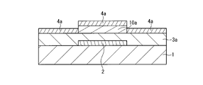
- FIG. 4A is a cross-sectional view showing a part of the process of the manufacturing method of the organic TFT.
- FIG. 4B is a cross-sectional view showing a step following FIG. 4A of the manufacturing method.
- FIG. 4C is a cross-sectional view showing a step following FIG. 4B of the manufacturing method.
- FIG. 4D is a cross-sectional view showing a step following FIG. 4C of the manufacturing method.
- FIG. 4A is a cross-sectional view showing a part of the process of the manufacturing method of the organic TFT.
- FIG. 4B is a cross-sectional view showing a step following FIG. 4A of the manufacturing method.
- FIG. 4C is a
- FIG. 4E is a cross-sectional view showing a step following FIG. 4D of the manufacturing method.
- FIG. 4F is a cross-sectional view showing a step following FIG. 4E of the same manufacturing method.
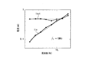
- FIG. 5 is a diagram showing an actual measurement example of the cutoff frequency characteristic of the organic TFT.
- FIG. 6 is a cross-sectional view showing another embodiment of the structure of the organic TFT.
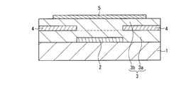
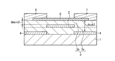
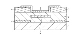
- FIG. 7 is a cross-sectional view showing the structure of the organic TFT in the second embodiment.
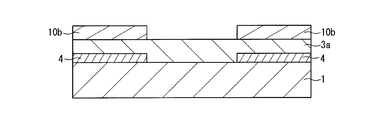
- FIG. 8A is a cross-sectional view showing a part of the process of the method for manufacturing the organic TFT.
- FIG. 8B is a cross-sectional view showing a step following FIG. 8A of the manufacturing method.
- FIG. 8C is a cross-sectional view showing a step following FIG. 8B of the same manufacturing method.
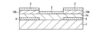
- FIG. 8D is a cross-sectional view showing a step following FIG. 8C of the same manufacturing method.
- FIG. 8E is a cross-sectional view showing a step following FIG. 8D of the manufacturing method.
- FIG. 8F is a cross-sectional view showing a step following FIG. 8E of the manufacturing method.
- FIG. 9 is a cross-sectional view showing another embodiment of the structure of the organic TFT.
- the organic thin film transistor of the present invention can take the following aspects based on the above configuration.
- the thickness of the gate insulating film interposed between the main gate electrode and the organic semiconductor film is different from the thickness of the gate insulating film interposed between the auxiliary gate electrode and the organic semiconductor film,
- the gate insulating film may be interposed between the main gate electrode and the auxiliary gate electrode.
- a certain voltage is applied to the auxiliary gate electrode, and the electric field between the auxiliary gate electrode and the organic semiconductor film is stronger than the electric field between the main gate electrode and the organic semiconductor film.
- the relationship between the thickness of the insulating film and the voltage applied to the auxiliary gate electrode and the main gate electrode can be set.
- the main gate electrode and the auxiliary gate electrode are formed so that there is no gap between the end portions in the projection in a direction orthogonal to the organic semiconductor film.
- the main gate electrode and the auxiliary gate electrode may be in a state where there is a slight overlap between the end portions.
- the main gate electrode and the auxiliary gate electrode are formed so that there is no overlapping area in projection in a direction orthogonal to the organic semiconductor film.
- the method for producing an organic thin film transistor of the present invention can take the following aspects based on the above configuration.
- the other gate electrode is changed to the one by the step including back exposure from the back surface side of the substrate using the gate electrode formed in the first gate film formation step as a mask. Patterning is performed in a self-aligned manner with respect to the electrodes. As a result, an optimum state in which there is no overlapping region or gap between both gates can be easily obtained.
- the gate insulating film is divided into a lower insulating film and an upper insulating film, and after the first gate film forming step, the lower insulating film is formed to cover the one gate electrode,
- the other gate electrode may be formed on the lower insulating film by a second gate film forming step, and then the upper insulating film may be formed to cover the other gate electrode.
- a main gate electrode 2 is provided on an insulating substrate 1, and a lower insulating film 3 a is formed so as to cover the main gate electrode 2.
- An auxiliary gate electrode 4 is formed on the upper surface of the lower insulating film 3a, and an upper insulating film 3b is formed to cover the upper surface of the auxiliary gate electrode 4.
- the lower insulating film 3a and the upper insulating film 3b constitute the gate insulating film 3. With this configuration, it is possible to obtain a state in which the main gate electrode 2 and the auxiliary gate electrode 4 are disposed in the gate insulating film 3 so as to be electrically separated from each other.
- An organic semiconductor film 5 is formed on the upper surface of the upper insulating film 3 b covering the auxiliary gate electrode 4, and a source electrode 6 and a drain electrode 7 are provided in contact with the organic semiconductor film 5.
- This organic TFT has a top contact type structure in which a source electrode 6 and a drain electrode 7 are formed on an organic semiconductor film 5.
- the element structure of the organic TFT is generally roughly classified into two types, a top contact type and a bottom contact type. As will be described later, the characteristics of the organic TFT of the present embodiment can be similarly applied to a bottom contact type, that is, a structure in which a source electrode and a drain electrode are formed below an organic semiconductor film.
- the main gate electrode 2 is disposed in a region facing the channel region between the source electrode 6 and the drain electrode 7 in the organic semiconductor film 5.
- the auxiliary gate electrode 4 is a pair of elements that are disposed on both sides of the main gate electrode 2 in regions facing the source electrode 6 and the drain electrode 7 respectively.
- the main gate electrode 2 and the auxiliary gate electrode 4 are electrically separated from each other. That is, the auxiliary gate electrode 4 is disposed at a position where the height from the upper surface of the substrate 1 is higher than that of the main gate electrode 2, and the gate insulating film 3 is interposed between the main gate electrode 2 and the auxiliary gate electrode 4. Yes.
- the thickness of the gate insulating film 3 interposed between the main gate electrode 2 and the organic semiconductor film 5, that is, the main gate insulating film thickness dmain1 is interposed between the auxiliary gate electrode 4 and the organic semiconductor film 5.
- the gate insulating film 3 is thicker than the auxiliary gate insulating film thickness dsub1.
- FIG. 1 An example of a circuit for driving the organic TFT is shown in FIG. That is, the main gate electrode 2 is applied with the main gate voltage VGmain, which is a constant DC voltage, and the modulation voltage VGsig from the modulation driver 8.
- the main gate voltage VGmain and the modulation voltage VGsig are not necessarily supplied separately, and a signal including a direct current component and a modulation component may be generated and supplied from the beginning.
- An auxiliary gate voltage VGsub which is a constant DC voltage, is applied to the auxiliary gate electrode 4 independently of the voltage of the main gate electrode 2.
- a drain voltage VD is applied to the drain electrode 7.
- the ammeter 9 shows the measurement location at the time of actually measuring the cutoff frequency characteristic described later.
- the channel length L indicates the length of the channel region of the organic semiconductor film 5.
- the channel resistance of the organic semiconductor film 5 is controlled by the main gate voltage VGmain applied to the main gate electrode 2 and the modulation voltage VGsig.
- an electric field having a high potential is always formed in the interface region between the organic semiconductor film 5 and the source electrode 6 and the drain electrode 7 by the auxiliary gate voltage VGsub.
- the contact resistance between the organic semiconductor film 5 and the source electrode 6 and the drain electrode 7 is controlled to be low.
- the channel resistance can be controlled in a state in which the influence of the contact resistance is sufficiently suppressed. That is, even in driving in a low voltage region, an operation with a sufficiently low contact resistance is possible in principle. Therefore, in a device having a short channel length L required for high-speed operation, the effective mobility of the transistor can be increased, and an organic TFT that can be driven at a remarkably high operating frequency can be obtained.
- the electric field between the auxiliary gate electrode 4 and the organic semiconductor film 5 is changed between the main gate electrode 2 and the organic gate electrode 2. It is desirable to set so as to be stronger than the electric field between the semiconductor films 5. That is, the sizes of the auxiliary gate voltage VGsub, main gate voltage VGmain, main gate insulating film thickness dmain1, and auxiliary gate insulating film thickness dsub1 are set so that VGsub / dsub1 is sufficiently larger than VGmain / dmain1. It is desirable. By satisfying this condition, the contact resistance between the organic semiconductor film 5 and the source electrode 6 and drain electrode 7 can be made sufficiently small, and a high transconductance can be obtained with a small gate voltage, which is extremely effective for high-speed operation. .
- the contact resistance is sufficiently reduced by VGsub (the electric field of VGsub / dsub1) without increasing VGmain (the electric field of VGmain / dmain1), and high mobility can be obtained.
- VGmain the electric field of VGmain / dmain1
- the main gate electrode 2 is opposed to the channel region, while the auxiliary gate electrode 4 is disposed so as to be opposed to the source electrode 6 and the drain electrode 7 on both sides of the channel region. Therefore, the parasitic capacitance between the main gate electrode 2 and the auxiliary gate electrode 4 is small, and the influence on the high-speed response is small.
- the main gate electrode 2 and the auxiliary gate electrode 4 are formed so that there is no overlapping area in the projection in the direction orthogonal to the organic semiconductor film 5 (direction orthogonal to the film surface). To do.
- the main gate electrode 2 and the auxiliary gate electrode 4 may have some overlapping area P in the projection in the direction perpendicular to the film surface. Even in such a case, the above-described effects are not substantially affected. Therefore, some errors in the formation of the electrode pattern are acceptable. However, it is desirable to avoid the state where a gap exists between the main gate electrode 2 and the auxiliary gate electrode 4 as much as possible in the projection in the direction perpendicular to the film surface.
- the main gate electrode 2 is formed on the substrate 1.
- the main gate electrode 2 is produced by patterning a metal film such as Au, Al, Cr, Cu, or Mo by photolithography or the like.
- a lower insulating film 3a is formed to cover the main gate electrode 2.
- the lower insulating film 3a is a first layer film constituting the gate insulating film 3, and is a polymer insulating film such as Cytop (amorphous fluororesin, registered trademark), BCB (benzocyclobutene), or Al 2 O 3 , An inorganic insulating film such as SiO 2 can be used. Further, a photoresist layer 10 is formed on the lower insulating film 3a.
- a back exposure process is performed in which the exposure light 11 is irradiated from the back side of the substrate 1 using the main gate electrode 2 as a photomask. Thereafter, development is performed, and the photoresist layer 10 is patterned to form a resist pattern 10a as shown in FIG. 4C. According to this back exposure process, the resist pattern 10a can be formed in a self-aligned manner with respect to the main gate electrode 2.
- a metal film 4a film for the auxiliary gate electrode 4
- made of Au, Al, Cr, Cu, Mo or the like is formed so as to cover the entire surface including the resist pattern 10a.
- the resist pattern 10a is removed with a resist stripping solution.
- the portion of the metal film 4a on the resist pattern 10a is removed by lift-off, and the auxiliary gate electrode 4 is patterned.
- the main gate electrode 2 and the auxiliary gate electrode 4 are formed in a self-aligning manner.
- an upper insulating film 3b is formed to cover the auxiliary gate electrode 4.
- the upper insulating film 3b is a second layer film constituting the gate insulating film 3, and is made of, for example, a polymer insulating film such as Cytop or BCB, or an inorganic insulating film such as Al 2 O 3 or SiO 2 .
- an organic semiconductor film 5 (for example, pentacene, DNTT (dinaphthothienothiophene), alkyl DNTT, etc.) is formed on the upper insulating film 3b.
- the source electrode 6 and the drain electrode 7 are formed on the upper surface of the end portion of the organic semiconductor film 5 by using, for example, Au and using a shadow mask or photolithography.
- the auxiliary gate electrode 4 can be formed in a self-aligned manner with respect to the main gate electrode 2, and the parasitic capacitance due to the gate electrode can be easily reduced. As a result, it is possible to produce a high-speed operation organic TFT capable of operating at a remarkably high frequency even in a low drive voltage region as compared with the conventional case.
- a method of forming the auxiliary gate electrode 4 in a self-aligned manner with respect to the main gate electrode 2 other known methods can be used.
- f T The current gain cutoff frequency
- This organic TFT has a configuration in which a main gate electrode 2, an auxiliary gate electrode 4, and a gate insulating film 3 are formed on an insulating substrate 1, and is the case of the top contact type organic TFT shown in FIG. It is the same.
- the source electrode 6 and the drain electrode 7 are formed on the upper surface of the gate insulating film 3 with a gap in a range corresponding to the channel region.
- An organic semiconductor film 5 is formed with the end portions disposed on the upper surfaces of the source electrode 6 and the drain electrode 7.
- the mutual relationship between the main gate electrode 2 and the auxiliary gate electrode 4 is exactly the same as the configuration shown in FIG. 1, and the same effect can be obtained by applying the above-described driving method described with reference to FIG. Can be obtained.
- the auxiliary gate electrode 4 is disposed on the insulating substrate 1, and the lower insulating film 3 a is formed to cover the auxiliary gate electrode 4.
- a main gate electrode 2 is formed on the upper surface of the lower insulating film 3a, and an upper insulating film 3b is formed to cover the upper surface of the main gate electrode 2. With this configuration, it is possible to obtain a state in which the main gate electrode 2 and the auxiliary gate electrode 4 are disposed separately from each other in the gate insulating film 3.
- An organic semiconductor film 5, a source electrode 6 and a drain electrode 7 are provided on the upper insulating film 3b.
- the main gate electrode 2 is disposed in a region facing the channel region between the source electrode 6 and the drain electrode 7 in the organic semiconductor film 5.
- the auxiliary gate electrode 4 is disposed in regions facing the source electrode 6 and the drain electrode 7 on both sides of the main gate electrode 2, and the auxiliary gate electrode 4 and the main gate electrode 2 are electrically separated from each other.
- the thickness of the gate insulating film 3 interposed between the main gate electrode 2 and the organic semiconductor film 5, that is, the main gate insulating film thickness dmain2 is the gate insulating film interposed between the auxiliary gate electrode 4 and the organic semiconductor film 5. 3 is thinner than the auxiliary gate insulating film thickness dsub2.
- the circuit for driving this organic TFT can basically be configured in the same manner as shown in FIG.
- the channel resistance of the organic semiconductor film 5 is controlled by the main gate voltage VGmain and the modulation voltage VGsig applied to the main gate electrode 2, and between the organic semiconductor film 5 and the source electrode 6 and drain electrode 7 by the auxiliary gate voltage VGsub.
- the contact resistance is controlled to be low.
- the electric field between the auxiliary gate electrode 4 and the organic semiconductor film 5 is changed between the main gate electrode 2 and the organic semiconductor. It is desirable to set so as to be stronger than the electric field between the films 5. That is, the magnitudes of the auxiliary gate voltage VGsub, main gate voltage VGmain, main gate insulating film thickness dmain2, and auxiliary gate insulating film thickness dsub2 are set so that VGsub / dsub2 is sufficiently larger than VGmain / dmain2. It is desirable. By satisfying this condition, the contact resistance between the organic semiconductor film 5 and the source electrode 6 and drain electrode 7 can be made sufficiently small, and a high transconductance can be obtained with a small gate voltage, which is extremely effective for high-speed operation. .
- the main gate electrode 2 and the auxiliary gate electrode 4 face different regions, the parasitic capacitance between the main gate electrode 2 and the auxiliary gate electrode 4 is small, and the influence on the high-speed response is small.
- the main gate electrode 2 and the auxiliary gate electrode 4 are formed so that there is no overlapping area in the projection in the direction perpendicular to the film surface.
- the main gate electrode 2 and the auxiliary gate electrode 4 may have some overlapping areas in the projection in the direction perpendicular to the film surface. Further, it is desirable to avoid the state where a gap exists between the main gate electrode 2 and the auxiliary gate electrode 4 as much as possible in the projection in the direction perpendicular to the film surface.
- the auxiliary gate electrode 4 is formed on the substrate 1.
- the auxiliary gate electrode 4 is produced by patterning a metal film such as Au, Al, Cr, Cu, or Mo by photolithography or the like.
- a lower insulating film 3a is formed to cover the auxiliary gate electrode 4.
- a polymer insulating film such as Cytop (registered trademark) or BCB, or an inorganic insulating film such as Al 2 O 3 or SiO 2 can be used.
- a photoresist layer 10 is formed on the lower insulating film 3a.
- a back exposure process from the back side of the substrate 1 is performed using the auxiliary gate electrode 4 as a photomask. Thereafter, development is performed, and the photoresist layer 10 is patterned to form a resist pattern 10b as shown in FIG. 8C.
- the resist pattern 10b can be patterned in a self-aligned manner with respect to the auxiliary gate electrode 4.
- a metal film 2a such as Au, Al, Cr, Cu, or Mo for forming the main gate electrode 2 is formed so as to cover the entire surface including the resist pattern 10b.
- the resist pattern 10b is removed with a resist stripping solution.
- the portion of the metal film 2a on the resist pattern 10b is removed by lift-off, and the main gate electrode 2 is patterned.
- the main gate electrode 2 and the auxiliary gate electrode 4 are formed in a self-aligning manner.
- an upper insulating film 3b is formed to cover the main gate electrode 2.
- the upper insulating film 3b is made of, for example, a polymer insulating film such as Cytop or BCB, or an inorganic insulating film such as Al 2 O 3 or SiO 2 .
- an organic semiconductor film 5 (for example, pentacene, DNTT, alkyl DNTT, etc.) is formed on the upper insulating film 3b.
- the source electrode 6 and the drain electrode 7 are formed on the upper surface of the end portion of the organic semiconductor film 5 by using, for example, Au or the like by a shadow mask or photolithography (see FIG. 7).
- the main gate electrode 2 can be formed in a self-aligned manner with respect to the auxiliary gate electrode 4, and the parasitic capacitance due to the gate electrode can be easily reduced.
- the present embodiment it is possible to manufacture a high-speed operation organic TFT capable of operating at a drastically high frequency in a low driving voltage region.
- This organic TFT has a configuration in which the auxiliary gate electrode 4, the main gate electrode 2, and the gate insulating film 3 are formed on the insulating substrate 1, and the case of the top contact type organic TFT shown in FIG. It is the same.
- a source electrode 6 and a drain electrode 7 are formed on the upper surface of the gate insulating film 3 with a gap in a range corresponding to the channel region.
- An organic semiconductor film 5 is formed with the end portions disposed on the upper surfaces of the source electrode 6 and the drain electrode 7.
- the interrelationship between the main gate electrode 2 and the auxiliary gate electrode 4 is exactly the same as that shown in FIG. 7 and is the same by applying the above-described driving method described with reference to FIG. It is possible to obtain the effect.
- the organic thin film transistor of the present invention can sufficiently improve the high-speed response performance by shortening the channel length.
- the active matrix backplane required for driving e-paper, liquid crystal, organic EL display, etc., pixel driving It is useful for all logic circuit elements that require high-speed operation, such as gates, source driver circuits, or RFID tags.
Landscapes
- Thin Film Transistor (AREA)
- Electrodes Of Semiconductors (AREA)
Abstract
Description
実施の形態1における有機TFTの構造を、図1に断面図で示す。絶縁性の基板1の上に、主ゲート電極2が設けられ、主ゲート電極2を覆って下部絶縁膜3aが形成されている。下部絶縁膜3aの上面に補助ゲート電極4が形成され、補助ゲート電極4の上面を覆って上部絶縁膜3bが形成されている。下部絶縁膜3aと上部絶縁膜3bによりゲート絶縁膜3が構成される。この構成により、ゲート絶縁膜3中に互いに電気的に分離させて、主ゲート電極2と補助ゲート電極4が配置された状態が得られる。補助ゲート電極4を覆った上部絶縁膜3bの上面に、有機半導体膜5が形成され、有機半導体膜5に接触させてソース電極6及びドレイン電極7が設けられている。
[1]測定に供した有機TFTの素子構成
主ゲート電極2:Au
下部絶縁膜3a:Al2O3、200nm
補助ゲート電極4:Au
上部絶縁膜3b:Al2O3、100nm
有機半導体膜5:C10-DNTTの塗布結晶膜
ソース電極6、ドレイン電極7:Au
チャネル長L:~2μm
[2]測定条件
補助ゲート電極4の電圧:VGsub=-20V
ドレイン電極7の電圧:VD=-10V
主ゲート電極2の電圧:主ゲート電圧VGmain=-5V、変調電圧VGsig=1VP-Pの正弦波電圧
以上のとおりの設定により、主ゲート電極2への入力電流(Iin)とトランジスタ出力電流(ドレイン電流、Iout)を同時計測した結果を、図5に示す。図5において、横軸は変調電圧VGsigの周波数(Hz)、縦軸は電流(mAP-P)である。
実施の形態2における有機TFTの構造を、図7に断面図で示す。この素子構造は、素子の厚み方向における主ゲート電極2と補助ゲート電極4の位置関係が、実施の形態1の場合と異なる以外は、実施の形態1と同様である。従って、実施の形態1の場合と同様の構成要素については、同一の参照符号を付して、説明を簡略化する。
2 主ゲート電極
3 ゲート絶縁膜
3a 下部絶縁膜
3b 上部絶縁膜
4 補助ゲート電極
5 有機半導体膜
6 ソース電極
7 ドレイン電極
8 変調駆動部
9 電流計
10 フォトレジスト層
10a、10b レジストパターン
11 露光光
Claims (8)
- 絶縁性の基板と、前記基板上に設けられたゲート電極と、前記ゲート電極を覆って形成されたゲート絶縁膜と、前記ゲート絶縁膜上に形成された有機半導体膜と、前記有機半導体膜に接触させて配置されたソース電極及びドレイン電極とを備え、
前記ゲート電極は、前記有機半導体膜における前記ソース電極と前記ドレイン電極の間のチャネル領域に対向する領域に配置された主ゲート電極と、前記主ゲート電極の両側で前記ソース電極及び前記ドレイン電極にそれぞれ対向する領域に配置された一対の補助ゲート電極とを含み、
前記主ゲート電極と前記補助ゲート電極とは互いに電気的に分離されていることを特徴とする有機薄膜トランジスタ。 - 前記主ゲート電極と前記有機半導体膜との間に介在する前記ゲート絶縁膜の厚さと、前記補助ゲート電極と前記有機半導体膜との間に介在する前記ゲート絶縁膜の厚さが異なり、前記主ゲート電極と前記補助ゲート電極の間に前記ゲート絶縁膜が介在している請求項1に記載の有機薄膜トランジスタ。
- 前記補助ゲート電極には一定の電圧を印加し、
前記補助ゲート電極と前記有機半導体膜間の電界が、前記主ゲート電極と前記有機半導体膜間の電界よりも強くなるように、前記ゲート絶縁膜の厚さと、前記補助ゲート電極及び前記主ゲート電極に印加する電圧の関係が設定されている請求項1または2に記載の有機薄膜トランジスタ。 - 前記主ゲート電極と前記補助ゲート電極は、前記有機半導体膜に直交する方向の射影において、端部間に隙間が存在しないように形成されている請求項1~3のいずれか1項に記載の有機薄膜トランジスタ。
- 前記主ゲート電極と前記補助ゲート電極は、前記有機半導体膜に直交する方向の射影において重畳する面積が存在しないように形成されている請求項4に記載の有機薄膜トランジスタ。
- 請求項1に記載の有機薄膜トランジスタを製造する方法であって、
前記絶縁性の基板上に前記主ゲート電極及び前記補助ゲート電極のうちの一方のゲート電極を形成し、
前記一方のゲート電極を覆って下部ゲート絶縁膜を形成し、
前記下部ゲート絶縁膜上に他方の前記ゲート電極を形成し、
前記他方のゲート電極及び前記下部ゲート絶縁膜を覆って上部ゲート絶縁膜を形成し、
前記上部ゲート絶縁膜上に有機半導体膜を形成するとともに、前記有機半導体膜に接触させてソース電極及びドレイン電極とを形成することを特徴とする有機薄膜トランジスタの製造方法。 - 前記第2ゲート成膜工程では、前記第1ゲート成膜工程で形成されたゲート電極をマスクとする前記基板の裏面側からの背面露光を含む工程により、前記他方のゲート電極を前記一方の電極に対して自己整合的にパターニングする請求項6に記載の有機薄膜トランジスタの製造方法。
- 前記ゲート絶縁膜を下部絶縁膜と上部絶縁膜に分けて成膜し、
前記第1ゲート成膜工程の後、前記一方のゲート電極を覆って前記下部絶縁膜を形成し、
その後、前記第2ゲート成膜工程により前記下部絶縁膜上に前記他方のゲート電極を形成し、
その後、前記他方のゲート電極を覆って前記上部絶縁膜を形成する請求項6または7に記載の有機薄膜トランジスタの製造方法。
Priority Applications (2)
| Application Number | Priority Date | Filing Date | Title |
|---|---|---|---|
| JP2014531619A JP5842262B2 (ja) | 2012-08-24 | 2013-08-19 | 有機薄膜トランジスタ及びその製造方法 |
| US14/423,401 US9379341B2 (en) | 2012-08-24 | 2013-08-19 | Organic thin film transistor and method for producing same |
Applications Claiming Priority (2)
| Application Number | Priority Date | Filing Date | Title |
|---|---|---|---|
| JP2012-185621 | 2012-08-24 | ||
| JP2012185621 | 2012-08-24 |
Publications (1)
| Publication Number | Publication Date |
|---|---|
| WO2014030613A1 true WO2014030613A1 (ja) | 2014-02-27 |
Family
ID=50149922
Family Applications (1)
| Application Number | Title | Priority Date | Filing Date |
|---|---|---|---|
| PCT/JP2013/072110 Ceased WO2014030613A1 (ja) | 2012-08-24 | 2013-08-19 | 有機薄膜トランジスタ及びその製造方法 |
Country Status (3)
| Country | Link |
|---|---|
| US (1) | US9379341B2 (ja) |
| JP (1) | JP5842262B2 (ja) |
| WO (1) | WO2014030613A1 (ja) |
Families Citing this family (4)
| Publication number | Priority date | Publication date | Assignee | Title |
|---|---|---|---|---|
| US9685526B2 (en) * | 2014-02-12 | 2017-06-20 | International Business Machines Corporation | Side gate assist in metal gate first process |
| JP6255651B2 (ja) * | 2014-03-07 | 2018-01-10 | 富士フイルム株式会社 | 薄膜トランジスタ |
| KR102303994B1 (ko) * | 2014-10-20 | 2021-09-23 | 삼성디스플레이 주식회사 | 유기발광 표시기판의 제조방법 |
| KR102801061B1 (ko) * | 2020-11-26 | 2025-04-28 | 엘지디스플레이 주식회사 | 표시 장치 |
Citations (4)
| Publication number | Priority date | Publication date | Assignee | Title |
|---|---|---|---|---|
| JPH09186332A (ja) * | 1995-12-28 | 1997-07-15 | Furontetsuku:Kk | 電界効果トランジスタおよびその駆動方法 |
| JP2007243001A (ja) * | 2006-03-10 | 2007-09-20 | Konica Minolta Holdings Inc | 有機薄膜トランジスタの製造方法及び有機薄膜トランジスタ |
| WO2011052058A1 (ja) * | 2009-10-29 | 2011-05-05 | パイオニア株式会社 | 有機薄膜トランジスタ |
| JP2011101030A (ja) * | 2008-08-04 | 2011-05-19 | Panasonic Corp | フレキシブル半導体装置およびその製造方法 |
Family Cites Families (4)
| Publication number | Priority date | Publication date | Assignee | Title |
|---|---|---|---|---|
| US7378715B2 (en) * | 2003-10-10 | 2008-05-27 | General Electric Company | Free-standing electrostatically-doped carbon nanotube device |
| US8896065B2 (en) * | 2008-04-14 | 2014-11-25 | Sharp Laboratories Of America, Inc. | Top gate thin film transistor with independent field control for off-current suppression |
| JP5501604B2 (ja) | 2008-12-04 | 2014-05-28 | シャープ株式会社 | 有機薄膜トランジスタ |
| KR20120024241A (ko) * | 2010-09-06 | 2012-03-14 | 삼성모바일디스플레이주식회사 | 유기 발광 디스플레이 장치 및 그 제조 방법 |
-
2013
- 2013-08-19 JP JP2014531619A patent/JP5842262B2/ja active Active
- 2013-08-19 US US14/423,401 patent/US9379341B2/en active Active
- 2013-08-19 WO PCT/JP2013/072110 patent/WO2014030613A1/ja not_active Ceased
Patent Citations (4)
| Publication number | Priority date | Publication date | Assignee | Title |
|---|---|---|---|---|
| JPH09186332A (ja) * | 1995-12-28 | 1997-07-15 | Furontetsuku:Kk | 電界効果トランジスタおよびその駆動方法 |
| JP2007243001A (ja) * | 2006-03-10 | 2007-09-20 | Konica Minolta Holdings Inc | 有機薄膜トランジスタの製造方法及び有機薄膜トランジスタ |
| JP2011101030A (ja) * | 2008-08-04 | 2011-05-19 | Panasonic Corp | フレキシブル半導体装置およびその製造方法 |
| WO2011052058A1 (ja) * | 2009-10-29 | 2011-05-05 | パイオニア株式会社 | 有機薄膜トランジスタ |
Also Published As
| Publication number | Publication date |
|---|---|
| US20150188063A1 (en) | 2015-07-02 |
| JP5842262B2 (ja) | 2016-01-13 |
| JPWO2014030613A1 (ja) | 2016-07-28 |
| US9379341B2 (en) | 2016-06-28 |
Similar Documents
| Publication | Publication Date | Title |
|---|---|---|
| TWI567995B (zh) | 薄膜電晶體及其製造方法 | |
| KR102127781B1 (ko) | 박막 트랜지스터 어레이 기판 및 그 제조 방법 | |
| CN102655095B (zh) | 薄膜晶体管及阵列基板的制造方法 | |
| CN103219391A (zh) | 一种薄膜晶体管及其制作方法、阵列基板和显示装置 | |
| KR20150063767A (ko) | 금속 산화물 반도체를 포함하는 박막 트랜지스터 기판 및 그 제조 방법 | |
| KR20150076405A (ko) | 디스플레이 장치의 정전기 방지 장치와 이의 제조 방법 | |
| CN104681631A (zh) | 薄膜晶体管及其制作方法、阵列基板及显示装置 | |
| TW200814386A (en) | Organic thin film transistor substrate and fabrication thereof | |
| JP5842262B2 (ja) | 有機薄膜トランジスタ及びその製造方法 | |
| KR101415484B1 (ko) | 유기 tft 어레이 기판 및 그 제조 방법 | |
| US9478612B2 (en) | Thin film transistor and display device using the same | |
| WO2017177498A1 (zh) | Tft基板及其制作方法 | |
| US20130048998A1 (en) | Semiconductor device, thin film transistor substrate, and display apparatus | |
| US10424672B2 (en) | Oxide semiconductor transistor | |
| CN102709240B (zh) | 阵列基板的制作方法、阵列基板和显示装置 | |
| JP7304813B2 (ja) | 画素ユニット及びその作製方法、アレイ基板 | |
| JP5370637B2 (ja) | 薄膜トランジスタ、アクティブマトリックス回路並びに表示装置 | |
| US10802363B2 (en) | Array substrate and manufacturing method therefor, display device and driving method therefor | |
| CN106024811B (zh) | 显示基板及其制作方法、显示器件 | |
| US20080206914A1 (en) | Patterning self-aligned transistors using back surface illumination | |
| CN112437985A (zh) | 阵列基板、显示器装置和制造阵列基板的方法 | |
| CN104992985A (zh) | 薄膜晶体管及其制造方法、阵列基板 | |
| JP6257027B2 (ja) | 有機薄膜トランジスタの製造方法 | |
| WO2011135945A1 (ja) | 半導体装置、表示装置、並びに半導体装置及び表示装置の製造方法 | |
| KR101273671B1 (ko) | 산화물 반도체 박막 트랜지스터 제조방법, 이에 따라 제조된 산화물 반도체 박막 트랜지스터를 포함하는 디스플레이 장치 및 능동구동센서 장치 |
Legal Events
| Date | Code | Title | Description |
|---|---|---|---|
| 121 | Ep: the epo has been informed by wipo that ep was designated in this application |
Ref document number: 13830468 Country of ref document: EP Kind code of ref document: A1 |
|
| ENP | Entry into the national phase |
Ref document number: 2014531619 Country of ref document: JP Kind code of ref document: A |
|
| WWE | Wipo information: entry into national phase |
Ref document number: 14423401 Country of ref document: US |
|
| NENP | Non-entry into the national phase |
Ref country code: DE |
|
| 122 | Ep: pct application non-entry in european phase |
Ref document number: 13830468 Country of ref document: EP Kind code of ref document: A1 |