WO2014025047A1 - 光学素子の製造方法、及びこの光学素子を用いた露光方法 - Google Patents
光学素子の製造方法、及びこの光学素子を用いた露光方法 Download PDFInfo
- Publication number
- WO2014025047A1 WO2014025047A1 PCT/JP2013/071727 JP2013071727W WO2014025047A1 WO 2014025047 A1 WO2014025047 A1 WO 2014025047A1 JP 2013071727 W JP2013071727 W JP 2013071727W WO 2014025047 A1 WO2014025047 A1 WO 2014025047A1
- Authority
- WO
- WIPO (PCT)
- Prior art keywords
- optical element
- substrate
- shape
- element substrate
- load
- Prior art date
- Legal status (The legal status is an assumption and is not a legal conclusion. Google has not performed a legal analysis and makes no representation as to the accuracy of the status listed.)
- Ceased
Links
Images




Classifications
-
- G—PHYSICS
- G03—PHOTOGRAPHY; CINEMATOGRAPHY; ANALOGOUS TECHNIQUES USING WAVES OTHER THAN OPTICAL WAVES; ELECTROGRAPHY; HOLOGRAPHY
- G03F—PHOTOMECHANICAL PRODUCTION OF TEXTURED OR PATTERNED SURFACES, e.g. FOR PRINTING, FOR PROCESSING OF SEMICONDUCTOR DEVICES; MATERIALS THEREFOR; ORIGINALS THEREFOR; APPARATUS SPECIALLY ADAPTED THEREFOR
- G03F1/00—Originals for photomechanical production of textured or patterned surfaces, e.g., masks, photo-masks, reticles; Mask blanks or pellicles therefor; Containers specially adapted therefor; Preparation thereof
- G03F1/60—Substrates
-
- B—PERFORMING OPERATIONS; TRANSPORTING
- B24—GRINDING; POLISHING
- B24B—MACHINES, DEVICES, OR PROCESSES FOR GRINDING OR POLISHING; DRESSING OR CONDITIONING OF ABRADING SURFACES; FEEDING OF GRINDING, POLISHING, OR LAPPING AGENTS
- B24B37/00—Lapping machines or devices; Accessories
- B24B37/04—Lapping machines or devices; Accessories designed for working plane surfaces
- B24B37/042—Lapping machines or devices; Accessories designed for working plane surfaces operating processes therefor
Definitions
- the present invention relates to a manufacturing method of an optical element applied when manufacturing an optical element such as a photomask used in an exposure apparatus, and an exposure method using the optical element manufactured by this manufacturing method.
- both sides of the photomask substrate are processed so as to be flat (flat) (see, for example, Patent Document 1).
- the peripheral portion of the photomask is supported and horizontally disposed by a holding mechanism or the like that the exposure apparatus has.
- the present invention is such that when an optical element such as a photomask is horizontally arranged in the exposure apparatus, both surfaces (upper surface and lower surface) of the optical element such as the photomask are flat.
- An object of the present invention is to provide an optical element manufacturing method capable of avoiding a situation that affects the imaging performance of an exposure apparatus.
- Another object of the present invention is to provide an exposure method using an optical element manufactured by such a manufacturing method.
- the manufacturing method of the 1st optical element which concerns on this invention is a manufacturing method of the optical element (1) which creates and processes both surfaces (9b, 9c) of the board
- the optical element substrate (9) is disposed substantially horizontally with a peripheral edge (9a) supported, and the both surfaces (9b, 9c) are formed when the vicinity of the center (9d) is suspended by its own weight.
- One surface (9b) is a predetermined convex surface and the other surface (9c) is a predetermined surface before the peripheral edge portion (9a) is supported and disposed substantially horizontally so as to be substantially flat.
- the creation process is A target shape calculation step of calculating the shapes of the predetermined convex surface and the predetermined concave surface of the optical element substrate (9); A shape measuring step for measuring the shape of the both surfaces (9b, 9c) of the optical element substrate (9) in a state where the vicinity of the center portion (9d) does not hang down by its own weight; The optical in a state where the vicinity of the center (9d) is not drooping due to the shape of the predetermined convex surface of the optical element substrate (9) calculated in the target shape calculation step and the own weight measured in the shape measurement step.
- the distribution of the load (W) applied to the plurality of loading regions (A) of the optical element substrate (9) is determined. And the vicinity of the center portion (9d) is not drooping due to the shape of the predetermined concave surface of the optical element substrate (9) calculated in the target shape calculation step and the own weight measured in the shape measurement step.
- the distribution of the load (W) applied to the plurality of loading regions (A) of the optical element substrate (9) is determined.
- the optical element substrate (9) is placed on the upper side of the polishing surface (7a) of the polishing means (8), and the load region (A) is loaded according to the load (W) distribution determined in the load distribution determination step. With the load (W) applied, the polishing surface (7a) is moved relative to the optical element substrate (9) to thereby move the one surface (9b) of the optical element substrate (9).
- the substrate creation process for creating the other surface (9c) The shape of the one surface (9b) of the optical element substrate (9) created in the substrate creation process and the shape of the predetermined convex surface of the optical element substrate calculated in the target shape calculation step Or the shape of the other surface (9c) of the optical element substrate (9) created in the substrate creation process and the optical element substrate (9 calculated in the target shape calculation step) And a shape determining step of finishing the processing when the difference from the shape of the predetermined concave surface falls within a predetermined allowable range.
- the optical element substrate is a photomask substrate
- both surfaces (upper surface and lower surface) of the photomask are flat. It is possible to avoid a situation that affects the imaging performance of the exposure apparatus.
- FIG. 6 is a diagram illustrating a part of a software display screen for determining weight distribution in the photomask manufacturing method according to the first embodiment.
- (C) is a figure which shows an example after final polishing
- (d) is a figure which shows another example after final polishing.
- the manufacturing method of the photomask which concerns on Example 1 it is a line graph which shows transition of the flatness of the lower surface and upper surface of a photomask substrate. It is the schematic of the exposure apparatus used for the method of Embodiment 2 of this invention.
- Embodiment 1 of the Invention 1 to 4 are diagrams according to Embodiment 1 of the present invention.
- the optical element according to the first embodiment is a photomask 1 made of rectangular plate-shaped quartz glass having a predetermined size (for example, length 1220 mm, width 1400 mm, thickness 13 mm),
- the exposure apparatus 2 is used by being arranged substantially horizontally with the peripheral edge 1a supported.
- the photomask 1 is held in the exposure apparatus 2 through a holding unit such as a mask holder, for example.
- the photomask 1 has its own weight in the thickness direction of the photomask 1 in a vertically standing state (a state in which the vertical direction or the horizontal direction extends vertically). Since it does not act in the horizontal direction (that is, in the horizontal direction), the upper surface 1b becomes a convex surface with a predetermined curvature, and the lower surface 1c becomes a concave surface with a predetermined curvature.
- the weight of the photomask 1 is determined in the thickness direction of the photomask 1 (that is, As shown by a solid line in FIG.
- the upper surface 1b and the lower surface 1c are both flat (horizontal plane). Therefore, unlike the conventional photomask in which the photomask 1 is bent by its own weight and has a curved upper surface and lower surface when placed horizontally on the exposure apparatus 2, a situation that affects the imaging performance of the exposure apparatus 2 is avoided. It becomes possible to do.
- both surfaces upper surface 1b and lower surface 1c
- the lower surface 1c is previously formed as a concave surface with a predetermined curvature and the upper surface 1b is formed with a convex surface with a predetermined curvature.
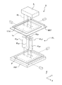
- a photomask substrate (optical element substrate) 9 having a predetermined size is prepared, and the upper surface 9b of the photomask substrate 9 is divided into six equal parts in the vertical and horizontal directions.
- 36 loading areas A A1 in the vicinity of the peripheral edge 9a, A2 in the vicinity of the center 9d, and A3 between A1 and A2 are defined on the photomask substrate 9.
- the peripheral portion is formed by creating the photomask substrate 9 described below in accordance with the procedure (steps S1 to S13) of the flowchart shown in FIG.
- the lower surface 9c becomes a concave surface having a predetermined curvature.
- the photomask substrate 9 is formed so that the upper surface 9b is a convex surface having a predetermined curvature.
- a concave surface having a predetermined curvature (and / or a predetermined flatness) is formed on the lower surface 9c of the photomask substrate 9 (steps S1 to S6).
- the target shape of the lower surface 9c of the photomask substrate 9 is calculated on the condition of the specifications of the exposure apparatus and the characteristics of the substrate related to the deflection amount (step S1).
- the process proceeds to the first bottom surface shape measuring step, and the current state (that is, photo) of the bottom surface 9c of the photomask substrate 9 is measured by a flatness measuring device (not shown) with the photomask substrate 9 standing vertically.
- the shape of the lower surface 9c of the mask substrate 9 is measured (step S2).
- Step S3 The distribution of weights (weights) W made of brass of a rectangular plate having a predetermined size and weight (for example, 135 mm in length, 155 mm in width, 20 mm in thickness, 3.5 kg in weight) to be loaded on each loading area A is determined. (Step S3).
- the peripheral portion 9 a of the photomask substrate 9 is increased in order to increase the processing amount in the vicinity of the central portion 9 d than in the vicinity of the peripheral portion 9 a of the photomask substrate 9.
- the distribution of the weights W is determined so that more weights W are placed near the center portion 9d than in the vicinity and a large load is applied. For example, as shown in FIG. 3, among the 36 loading areas A, 20 loading areas A1 corresponding to the vicinity of the peripheral edge 9a of the photomask substrate 9 (portions lightly displayed in FIG. 3A). Two weights W are respectively mounted, and four weights W are respectively mounted on four loading areas A2 (parts darkly shown in FIG. 3A) corresponding to the vicinity of the center portion 9d of the photomask substrate 9; The distribution of the weights W is determined so that the three weights W are placed on the remaining twelve loading areas A3 (portions indicated by intermediate darkness in FIG. 3A).
- step S4 primary generation processing is performed on the lower surface 9c of the photomask substrate 9 using a predetermined single-side polishing apparatus 8 (step S4).
- this single-side polishing apparatus 8 has a machine body 5 as shown in FIG. 4, and a disk-shaped lower surface plate 7 is rotatable on the machine body 5 in the direction of arrow M around a predetermined axis CT1. Is attached.
- a disk-shaped carrier 6 having a diameter smaller than that of the lower surface plate 7 is mounted so as to be rotatable in the direction of arrow N around the axis center CT 2 that is eccentric from the axis center CT 1 of the lower surface plate 7.
- a rectangular guide hole 6 a for guiding the photomask substrate 9 is formed through the center of the carrier 6.
- the arrow M direction and the arrow N direction are the same direction (counterclockwise as viewed from above the single-side polishing apparatus 8), as shown in FIG.
- the distribution of the weight W determined in step S3 that is, the central portion 9d compared to the vicinity of the peripheral portion 9a of the photomask substrate 9.
- the weight W is placed on the loading area A of the photomask substrate 9 according to a distribution in which many weights W are placed in the vicinity.
- the lower surface plate 7 is moved in the direction of arrow M about the axis CT1. While rotating at a predetermined rotation speed, the carrier 6 is rotated together with the photomask substrate 9 in the direction of arrow N around the axis CT2 at substantially the same rotation speed. Then, the polishing surface 7a of the lower surface plate 7 is in relation to the lower surface 9c of the photomask substrate 9 with the abrasive interposed between the polishing surface 7a of the lower surface plate 7 and the lower surface 9c of the photomask substrate 9. The relative movement is performed, and the lower surface 9c of the photomask substrate 9 is subjected to primary generation processing evenly by the abrasive.
- step S2 the photomask substrate 9 is set upright, and the flatness measuring device is used to measure the current state of the bottom surface 9c of the photomask substrate 9 (that is, The shape of the lower surface 9c of the photomask substrate 9 is measured immediately after the primary creation process (step S5).
- the process proceeds to the lower surface shape determination step, where a difference between the target shape of the lower surface 9c of the photomask substrate 9 and the current shape obtained in step S5 is obtained, and whether or not this difference is within a predetermined allowable range. Is determined (step S6).
- the predetermined allowable range can be arbitrarily set according to the required processing accuracy.
- steps S3 to S6 are repeated.
- the distribution of the weight W in step S3 performed when the procedure is repeated determines the target shape of the lower surface 9c of the photomask substrate 9 and the current shape obtained in the immediately lower surface shape determination step (step S6). This can be done based on the difference from the shape (the shape immediately after the primary creation process).
- a concave surface having a predetermined target value is formed on the lower surface 9c of the photomask substrate 9.
- the predetermined target value for the lower surface 9c can be set to, for example, 30 ⁇ m in flatness.
- the lower surface 9c is a concave surface in which the center portion 9d is recessed by 30 ⁇ m with respect to the peripheral edge portion 9a.
- the predetermined target value may be the curvature of the lower surface 9c (vertical curvature, lateral curvature, etc.).
- the curvature of the lower surface 9c reaches a predetermined target value, the lower surface 9c becomes a concave surface having the curvature.
- the target value may be both flatness and curvature.
- a convex surface having a predetermined curvature (and / or a predetermined flatness) is formed on the upper surface 9b of the photomask substrate 9 (steps S7 to S12).
- the target shape of the upper surface 9b of the photomask substrate 9 is calculated on the condition of the specifications of the exposure apparatus and the characteristics of the substrate related to the deflection amount (step S7).
- the process proceeds to the first upper surface shape measurement step, and the photomask substrate 9 is set upright, and the flatness measuring device is used to measure the current upper surface 9b of the photomask substrate 9 (that is, the photomask substrate 9).
- the shape of the upper surface 9b before processing is measured (step S8).
- step S9 the process proceeds to an upper surface load distribution determining step, and based on the difference between the target shape obtained in step S7 and the current shape obtained in step S8 on the upper surface 9b of the photomask substrate 9, the photomask substrate.
- the distribution of the weight W to be loaded on each loading area A is determined (step S9).
- the distribution of the weight W is determined so that a larger load acts on the weight 9 in the vicinity of the peripheral portion 9a than in the vicinity of the center portion 9d of the photomask substrate 9. For example, as shown in FIG. 3, among the 36 loading areas A, 20 loading areas A1 corresponding to the vicinity of the peripheral edge 9a of the photomask substrate 9 (portions lightly displayed in FIG. 3A).
- weights W are respectively mounted, and two weights W are respectively mounted on four loading areas A2 (parts darkly shown in FIG. 3A) corresponding to the vicinity of the center portion 9d of the photomask substrate 9.
- the distribution of the weights W is determined so that the three weights W are placed on the remaining twelve loading areas A3 (portions indicated by intermediate darkness in FIG. 3A).
- step S10 the process proceeds to the upper surface generation processing step, and the same procedure as step S4 described above is performed with the photomask substrate 9 turned upside down and the upper surface 9b in contact with the polishing surface 7a of the lower surface plate 7 of the single-side polishing apparatus 8.
- primary generation processing is performed on the upper surface 9b of the photomask substrate 9 using the single-side polishing apparatus 8 (step S10).
- step S8 the photomask substrate 9 is set up vertically, and the flatness measuring device is used to measure the current upper surface 9b of the photomask substrate 9 (that is, The shape of the upper surface 9b of the photomask substrate 9 is measured (immediately after the primary creation process) (step S11).
- the process proceeds to an upper surface shape determination step, where a difference between the target shape of the upper surface 9b of the photomask substrate 9 and the current shape obtained in step S11 is obtained, and whether or not this difference is within a predetermined allowable range. Is determined (step S12).
- the predetermined allowable range can be arbitrarily set according to the required processing accuracy.
- steps S9 to S12 are repeated.
- the distribution of the weight W in step S9 that is performed when the procedure is repeated determines the target shape and the current shape of the upper surface 9b of the photomask substrate 9 obtained in the immediately preceding upper surface shape determination step (step S12). This can be done based on the difference from the shape (the shape immediately after the primary creation process). If this difference falls within a predetermined allowable range, a convex surface having a predetermined target value is formed on the upper surface 9b of the photomask substrate 9.
- the predetermined target value for the upper surface 9b can be set to, for example, 30 ⁇ m in flatness.
- the upper surface 9b is a convex surface having a shape in which the central portion 9d protrudes by 30 ⁇ m from the peripheral portion 9a.
- the predetermined target value may be the curvature of the lower surface 9b (vertical curvature, lateral curvature, etc.).
- the upper surface 9b becomes a convex surface having the curvature.
- the target value may be both flatness and curvature.
- the process proceeds to the substrate finishing step, and the upper and lower surfaces (upper surface 9b and lower surface 9c) of the photomask substrate 9 are finish-polished using a predetermined double-side polishing apparatus (not shown), and then the photomask The substrate 9 is cleaned (step S13).
- the creation process of the photomask substrate 9 is completed, and the photomask 1 is completed by performing a commonly used process such as patterning on the photomask substrate 9.
- the weight W having a predetermined size has been described.
- the number of the loading areas A can be increased.
- the convex shape of the upper surface 9b and the concave shape of the lower surface 9c of the photomask substrate 9 can be further desired (desired curvature and / or desired flatness). Accordingly, the flatness of the upper surface 1b and the lower surface 1c when the photomask 1 is horizontally arranged in the exposure apparatus 2 is further improved.
- the weight W made of rectangular plate brass is used has been described.
- the shape and material of the weight W are not particularly limited.
- a container (not shown) corresponding to each loading area A may be prepared, and powder, liquid, or the like may be put in the container as a weight W.
- the target shape calculated in steps S1 and S7 is a flat surface instead of a concave surface or a convex surface, and in steps S3 and S9, the lower surface 9c and the upper surface 9b of the photomask substrate 9 are formed.
- the distribution of the weight W may be determined based on the difference between the current shape and the target shape (plane), and the weight W may be arranged according to this distribution to perform creation processing.
- step S4 a case where primary generation processing is performed on the photomask substrate 9 using the single-side polishing apparatus 8 in the lower surface generation processing step (step S4) and the upper surface generation processing step (step S10).
- polishing means other than the single-side polishing apparatus 8 (for example, a lapping apparatus).
- the optical element is the photomask 1
- an optical element other than the photomask 1 for example, a reticle mask for semiconductor, a wavefront forming optical element for radiation, a projection / illumination system, etc.
- the present invention can be similarly applied to a lens distortion correction optical element or the like.
- Example 1> 5 to 8 are diagrams according to Example 1 of Embodiment 1 of the present invention.
- a photomask substrate 9 made of quartz glass having a rectangular plate shape with a length of 1220 mm, a width of 1400 mm, and a thickness of 13 mm was prepared, and the photomask 1 was manufactured according to the procedure of the first embodiment described above.
- the software S captures, as input data, the difference between the target shape of the lower surface 9c and the upper surface 9b of the photomask substrate 9 and the current shape, and uses the difference as the first color. Is displayed in the display area D1. Alternatively, flatness data may be displayed in the display area D1. Then, after calculating the number of weights W placed on each loading area A of the photomask substrate 9 based on this input data, the output data includes the second number of weights W for each loading area A in a different color. Displayed in the display area D2. The output data displayed in this way can be changed manually by the operator's judgment if necessary. As a result, for example, fine adjustment or the like can be added to the output data as necessary.
- the target values of the lower surface 9c and the upper surface 9b of the photomask substrate 9 are both 30 ⁇ m in flatness. That is, the target shape of the lower surface 9c is a concave surface having a predetermined curvature in which the central portion 9d is recessed by 30 ⁇ m with respect to the peripheral portion 9a, and the target shape of the upper surface 9b is a predetermined shape in which the central portion 9d protrudes by 30 ⁇ m with respect to the peripheral portion 9a.
- the convex surface of the curvature In the present example, in order to achieve the above target value, the primary creation processing of the photomask substrate 9 had to be performed 8 times for each of the lower surface 9c and the upper surface 9b. Further, the final polishing of the photomask substrate 9 was performed seven times for each of the lower surface 9c and the upper surface 9b.
- the lower surface 9c of the photomask substrate 9 approaches a concave surface having a predetermined curvature as the primary creation process and the finish polishing process proceed.
- the display area D1 since different colors are displayed in the display area D1 according to the difference between the current shape of the lower surface 9c and the plane, if the lower surface 9c is a concave surface having a predetermined curvature, the display area D1 has a concentric shape. It is understood that the color scheme appears.
- an irregular color scheme deviating from the concentric color scheme corresponding to the concave surface having a predetermined curvature is displayed in the first display area D1 of the software S.
- FIG. 6 (b) showing an example of the state after the primary creation process
- FIG. 6 (c) showing an example of the state after the finish polishing process
- FIG. 6 (d) showing another example. Then, a color scheme close to the concentric color scheme corresponding to the concave surface having a predetermined curvature is displayed in the first display area D1 of the software S.
- FIG. 7 it was confirmed that the upper surface 9b of the photomask substrate 9 approaches a convex surface having a predetermined curvature as the primary creation process and the finish polishing process proceed. That is, in the state before processing, as shown in FIG. 7A, an irregular color scheme deviating from the concentric color scheme corresponding to the convex surface having a predetermined curvature is displayed in the first display area D1 of the software S.
- FIG. 7B showing an example of the state after the primary creation process
- FIG. 7C showing an example of the state after the finish polishing process
- FIG. 7D showing another example. Then, a color scheme close to the concentric color scheme corresponding to the convex surface having a predetermined curvature is displayed in the first display area D1 of the software S.
- the line graph of FIG. 8 shows the change in flatness of the lower surface 9c and the upper surface 9b of the photomask substrate 9 in detail.
- the horizontal axis represents time (the number of machining operations), and the vertical axis represents flatness (unit: ⁇ m).
- the flatness approaches the target value of 30 ⁇ m as the lower surface 9 c and the upper surface 9 b are repeatedly subjected to the primary creation process, and the target value is obtained by finish polishing. Was observed to be maintained.
- the flatness data is stored in the first display area D1 in the lower surface load distribution determining step (step S3) and the upper surface load distribution determining step (step S9).
- the case of displaying is described.
- the flatness data is set in the lower surface shape determining step (step S6) and the upper surface shape determining step (step S12).
- a value obtained by subtracting the data from the target value may be displayed. In this way, although it is actually finished with an uneven surface, it is displayed on the software S in the same way as normal polishing for flat finishing. It is possible to avoid the situation where the work is confused and the work is lost.
- the photomask 1 (FIG. 1) has the lower surface 9c formed as a concave surface with a predetermined curvature and the upper surface 9b formed as a convex surface with a predetermined curvature using the method of manufacturing an optical element according to the first embodiment. It can be obtained by subjecting the photomask substrate 9 to processes such as chromium film formation, resist coating, exposure / development, chromium film etching, resist peeling, defect correction, and pellicle sticking. As an example, the photomask 1 thus obtained has a predetermined pattern such as a circuit pattern formed on the lower surface 1c.
- the above processing can be performed in a state where the photomask substrate 9 (FIG. 3) is supported at the peripheral edge portion 9a and the lower surface 9c and the upper surface 9b extend in the horizontal direction. At this time, the vicinity of the center portion 9d of the photomask substrate 9 hangs down by its own weight, and both the lower surface 9c and the upper surface 9b are flat (horizontal plane). Therefore, in the present embodiment, the above-described processes such as chromium film formation, resist coating, exposure / development, etc. on the photomask substrate 9 are not affected by the shape change due to the deflection of the photomask substrate 9 and are in a suitable state. Can be done.
- the photomask 1 manufactured by the above process is placed on the exposure apparatus 2 having a schematic configuration shown in FIG. 9 and irradiated with the exposure light EL, so that the circuit pattern and the like formed on the photomask 1 are exposed. Projection exposure is performed on the substrate P or the like.
- the exposure apparatus 2 illuminates the mask stage MST for supporting the photomask 1, the substrate stage PST for supporting the photosensitive substrate P, and the photomask 1 supported by the mask stage MST with the exposure light EL.
- an optical projection system PL for projecting and exposing a circuit pattern of the photomask 1 illuminated with the exposure light EL onto the photosensitive substrate P supported by the substrate stage PST.
- Mask stage MST supports photomask 1 on the object plane side of projection optical system PL
- substrate stage PST supports photosensitive substrate P on the image plane side of projection optical system PL.
- the illumination optical system IL is composed of a plurality (five) of illumination system modules (not shown), and the projection optical system PL is also a plurality (five) of the illumination system modules corresponding to the number of illumination system modules.
- Projection optical systems PLa to PLe are provided. Each of the projection optical systems PLa to PLe is arranged corresponding to each of the five illumination system modules.
- the photomask 1 is formed using the photomask substrate 9 (FIG. 3) in which the lower surface 9c is formed as a concave surface with a predetermined curvature and the upper surface 9b is formed as a convex surface with a predetermined curvature.
- the pattern surface (lower surface 1c) and the upper surface 1b are both arranged in a plane (horizontal plane). Therefore, in the exposure method using the photomask 1, deterioration of the imaging performance due to the deflection of the photomask 1 is prevented.
- the exposure apparatus 2 shown in FIG. 9 is a multi-lens scan type exposure apparatus
- the exposure apparatus has one projection optical system, and the photomask 1 and the photosensitive substrate P are moved synchronously to form a pattern of the photomask 1.
- a step-and-repeat type in which the pattern of the photomask 1 is exposed while the photomask 1 and the photosensitive substrate P are stationary, and the photosensitive substrate P is sequentially moved stepwise.
- the present invention can also be applied to an exposure apparatus.
- the present invention can be widely applied when manufacturing an optical element such as a photomask used in an exposure apparatus. Further, it can be widely applied to an exposure method using the manufactured optical element.
Landscapes
- Engineering & Computer Science (AREA)
- Mechanical Engineering (AREA)
- Physics & Mathematics (AREA)
- General Physics & Mathematics (AREA)
- Preparing Plates And Mask In Photomechanical Process (AREA)
- Exposure And Positioning Against Photoresist Photosensitive Materials (AREA)
- Surface Treatment Of Glass (AREA)
Abstract
光学素子用基板9の両面を創成加工して成形する光学素子1の製造方法であって、光学素子用基板9は、自重によって中心部9d付近が下垂して前記両面がほぼ平面になるように略水平に配置される前の状態で一方の面9bが凸面になり、他方の面9cが凹面になるように創成加工される。 創成加工は、凸面および凹面の形状を算出する目標形状算出工程と、自重によって下垂していない状態における両面の形状を測定する形状測定工程と、目標形状算出工程で算出された算出結果と形状測定工程で測定された測定結果に基づき複数の載荷領域Aに作用させる荷重Wの分布を決定する荷重分布決定工程と、前記分布に従って荷重Wを作用させた状態で一方の面9bまたは他方の面9cを創成加工する基板創成加工工程と、創成加工された面と目標形状算出工程で算出された算出結果との差が所定の許容範囲に入れば加工を終了する形状判定工程とを含む。
Description
本発明は、露光装置に使用するフォトマスクなどの光学素子を製造する際に適用される光学素子の製造方法、及びこの製造方法によって製造された光学素子を用いた露光方法に関するものである。
従来、この種のフォトマスクを製造する際には、フォトマスク用基板の両面が平面(平坦)になるように加工する(例えば、特許文献1参照)。そして、このフォトマスクを露光装置に使用するときには、露光装置の有する保持機構等によってフォトマスクの周縁部を支持して水平に配置する。
しかしながら、このようなフォトマスクでは、露光装置に水平に配置されたときに、自重によって中心部近傍が下垂して両面(上面及び下面)が曲面になる傾向がある。例えば、縦1220mm、横1400mm、厚さ13mmの長方形板状の石英ガラスからなるフォトマスクでは、最も下垂する中心部が約60μmたわむという計算例もある。そして、露光装置に配置されたフォトマスクがたわむと、露光装置の結像性能に影響を及ぼすという課題があった。
本発明は、このような事情に鑑み、露光装置にフォトマスク等の光学素子が水平に配置されたとき、このフォトマスク等の光学素子の両面(上面及び下面)が平面になるようにすることで、露光装置の結像性能に影響を及ぼす事態を回避することが可能な光学素子の製造方法を提供することを目的とする。また本発明は、このような製造方法によって製造された光学素子を用いた露光方法を提供することを目的とする。
本発明に係る第1の光学素子の製造方法は、光学素子用基板(9)の両面(9b、9c)を創成加工して成形する光学素子(1)の製造方法であって、
前記光学素子用基板(9)は、周縁部(9a)が支持されて略水平に配置され、自重によって中心部(9d)付近が下垂した状態となった場合において前記両面(9b、9c)がほぼ平面になるように、前記周縁部(9a)が支持されて略水平に配置される前の状態で一方の面(9b)が所定の凸面になるとともに、他方の面(9c)が所定の凹面になるように創成加工され、
前記創成加工は、
前記光学素子用基板(9)の前記所定の凸面および前記所定の凹面の形状を算出する目標形状算出工程と、
自重によって中心部(9d)付近が下垂していない状態における前記光学素子用基板(9)の前記両面(9b、9c)の形状を測定する形状測定工程と、
前記目標形状算出工程で算出された前記光学素子用基板(9)の前記所定の凸面の形状と前記形状測定工程で測定された自重によって中心部(9d)付近が下垂していない状態における前記光学素子用基板(9)の前記一方の面(9b)の形状との差に基づき、前記光学素子用基板(9)の複数の載荷領域(A)に作用させる荷重(W)の分布を決定し、かつ前記目標形状算出工程で算出された前記光学素子用基板(9)の前記所定の凹面の形状と前記形状測定工程で測定された自重によって中心部(9d)付近が下垂していない状態における前記光学素子用基板(9)の前記他方の面(9c)の形状との差に基づき前記光学素子用基板(9)の複数の載荷領域(A)に作用させる荷重(W)の分布を決定する荷重分布決定工程と、
研磨手段(8)の研磨面(7a)の上側に前記光学素子用基板(9)を載置し、前記荷重分布決定工程で決定された荷重(W)の分布に従って前記載荷領域(A)に荷重(W)を作用させた状態で、前記光学素子用基板(9)に対して前記研磨面(7a)を相対移動させることにより、当該光学素子用基板(9)の前記一方の面(9b)または前記他方の面(9c)を創成加工する基板創成加工工程と、
前記基板創成加工工程で創成加工された前記光学素子用基板(9)の前記一方の面(9b)の形状と前記目標形状算出工程で算出された前記光学素子用基板の前記所定の凸面の形状との差、または前記基板創成加工工程で創成加工された前記光学素子用基板(9)の前記他方の面(9c)の形状と前記目標形状算出工程で算出された前記光学素子用基板(9)の前記所定の凹面の形状との差が所定の許容範囲に入れば加工を終了する形状判定工程とを含む光学素子の製造方法としたことを特徴とする。
なお、ここでは、本発明をわかりやすく説明するため、実施の形態を表す図面の符号に対応づけて説明したが、本発明が実施の形態に限定されるものでないことは言及するまでもない。
本発明によれば、光学素子用基板がフォトマスク用基板である場合には、露光装置にフォトマスクが水平に配置されたとき、このフォトマスクの両面(上面及び下面)が平面になるため、露光装置の結像性能に影響を及ぼす事態を回避することが可能となる。
以下、本発明の実施の形態について説明する。
[発明の実施の形態1]
図1乃至図4は、本発明の実施の形態1に係る図である。
図1乃至図4は、本発明の実施の形態1に係る図である。
この実施の形態1に係る光学素子は、図1に示すように、所定の大きさ(例えば、縦1220mm、横1400mm、厚さ13mm)の長方形板状の石英ガラスからなるフォトマスク1であり、図1(c)に示すように、露光装置2に周縁部1aが支持された状態で略水平に配置されて使用されるものである。露光装置2内におけるフォトマスク1の保持は、例えばマスクホルダ等の保持部を介して行われる。
そして、このフォトマスク1は、図1(b)に示すように、垂直に立てられた状態(縦方向又は横方向を垂直に延在させた状態)では、自重がフォトマスク1の厚さ方向(つまり、水平方向)に作用しないため、上面1bが所定の曲率の凸面になるとともに、下面1cが所定の曲率の凹面になる。しかし、図1(c)に二点鎖線によって示すように、フォトマスク1が露光装置2に周縁部1aを支持されて水平に配置されると、自重がフォトマスク1の厚さ方向(つまり、垂直方向)に作用し、図1(c)に実線で示すように、上面1bおよび下面1cがいずれも平面(水平面)になる。したがって、フォトマスク1では、露光装置2に水平に配置されたときに自重でたわんで上面および下面が曲面になる従来のフォトマスクと異なり、露光装置2の結像性能に影響を及ぼす事態を回避することが可能となる。
このようなフォトマスク1を製造する際には、フォトマスク1がその周縁部1aを支持されて水平に配置されたときに、フォトマスク1の自重によってフォトマスク1の中心部1d近傍が下垂して両面(上面1bおよび下面1c)が平面になるように、予め、下面1cが所定の曲率の凹面になるとともに、上面1bが所定の曲率の凸面になるように成形する。
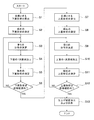
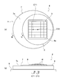
それには、まず、図3に示すように、所定の大きさのフォトマスク用基板(光学素子用基板)9を用意し、このフォトマスク用基板9の上面9bを縦横方向にそれぞれ6等分して格子状に区分して、フォトマスク用基板9上に36個の載荷領域A(周縁部9a近傍のA1、中心部9d近傍のA2、A1とA2の間のA3)を定義する。そして、フォトマスク1が水平に配置されたときの自重によるたわみを見込んで、図2に示すフローチャートの手順(ステップS1~S13)に従い、以下に述べるフォトマスク用基板9の創成加工により、周縁部9aが支持される前の状態(縦方向又は横方向を垂直に延在させた状態、または自重によって中心部9d付近が下垂していない状態)で、下面9cが所定の曲率の凹面になるとともに、上面9bが所定の曲率の凸面になるようにフォトマスク用基板9を成形する。
すなわち、このフォトマスク用基板9の創成加工では、最初に、フォトマスク用基板9の下面9cに所定の曲率(及び/又は所定の平面度)の凹面を形成する(ステップS1~S6)。
そのため、まず、下面目標形状算出工程で、露光装置の仕様や、たわみ量に関する基板の特性を条件として、フォトマスク用基板9の下面9cの目標とする形状を算出する(ステップS1)。
次いで、第1下面形状測定工程に移行し、フォトマスク用基板9を垂直に立てた状態で、平面度測定装置(図示せず)により、フォトマスク用基板9の下面9cの現在(つまり、フォトマスク用基板9の下面9cの加工前)の形状を測定する(ステップS2)。
その後、下面荷重分布決定工程に移行し、フォトマスク用基板9の下面9cの、ステップS1において求めた目標とする形状とステップS2において求めた現在の形状との差に基づき、フォトマスク用基板9の各載荷領域Aに載せる所定の大きさおよび重さ(例えば、縦135mm、横155mm、厚さ20mm、重さ3.5kg)の長方形板状の黄銅からなる重り(錘)Wの分布を決定する(ステップS3)。
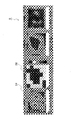
ここでは、フォトマスク用基板9の下面9cに凹面を形成するため、フォトマスク用基板9の周縁部9a近傍より中心部9d近傍の加工量を多くするべく、フォトマスク用基板9の周縁部9a近傍に比べて中心部9d近傍に多くの重りWが載って大きい荷重が作用するように、重りWの分布を決定する。例えば、図3に示すように、36個の載荷領域Aのうち、フォトマスク用基板9の周縁部9a近傍に対応する20個の載荷領域A1(図3(a)に淡く表示した部分)にそれぞれ2個の重りWが載り、フォトマスク用基板9の中心部9d近傍に対応する4個の載荷領域A2(図3(a)に濃く表示した部分)にそれぞれ4個の重りWが載り、残りの12個の載荷領域A3(図3(a)に中間の濃さで表示した部分)にそれぞれ3個の重りWが載るように重りWの分布を決定する。
次いで、下面創成加工工程に移行し、図4に示すように、所定の片面研磨装置8を用いて、フォトマスク用基板9の下面9cに対して1次創成加工を行う(ステップS4)。
すなわち、この片面研磨装置8は、図4に示すように、機体5を有しており、機体5には円盤状の下定盤7が所定の軸心CT1を中心として矢印M方向に回転駆動自在に取り付けられている。また、下定盤7の上側には、下定盤7より小径の円盤状のキャリア6が、下定盤7の軸心CT1から偏心した軸心CT2を中心として矢印N方向に回転駆動自在に載置されている。このキャリア6の中央部には、フォトマスク用基板9をガイドするための長方形のガイド孔6aが貫通して形成されている。なお、矢印M方向と矢印N方向とは、図4(a)に示すように、同じ方向(片面研磨装置8の上方から見て反時計方向)となっている。
そして、この片面研磨装置8を用いて、フォトマスク用基板9の下面9cに対して1次創成加工を行う際には、キャリア6のガイド孔6aにフォトマスク用基板9を設置することにより、下定盤7の研磨面7aの上側にフォトマスク用基板9を載置した後、ステップS3で決定された重りWの分布(つまり、フォトマスク用基板9の周縁部9a近傍に比べて中心部9d近傍に多くの重りWが載るような分布)に従ってフォトマスク用基板9の載荷領域Aに重りWを載せて荷重を作用させる。この状態で、下定盤7の研磨面7aとフォトマスク用基板9の下面9cとの間に研磨材(図示せず)を供給しつつ、下定盤7を軸心CT1を中心として矢印M方向に所定の回転速度で回転させるとともに、キャリア6をフォトマスク用基板9とともに軸心CT2を中心として矢印N方向にほぼ同一の回転速度で回転させる。すると、下定盤7の研磨面7aとフォトマスク用基板9の下面9cとの間に前記研磨材が介在した状態で、フォトマスク用基板9の下面9cに対して下定盤7の研磨面7aが相対移動し、フォトマスク用基板9の下面9cは前記研磨材によって均等に1次創成加工される。
このとき、フォトマスク用基板9の載荷領域Aには、上述したとおり、フォトマスク用基板9の周縁部9a近傍に比べて中心部9d近傍に多くの重りWが載っているので、フォトマスク用基板9の下面9cは、フォトマスク用基板9の周縁部9aから中心部9dに向かうほど、この1次創成加工によって除去される量が多くなる。その結果、フォトマスク用基板9の下面9cに凹面が形成される。
その後、第2下面形状測定工程に移行し、ステップS2と同様、フォトマスク用基板9を垂直に立てた状態で、前記平面度測定装置により、フォトマスク用基板9の下面9cの現在(つまり、フォトマスク用基板9の下面9cの1次創成加工直後)の形状を測定する(ステップS5)。
次いで、下面形状判定工程に移行し、フォトマスク用基板9の下面9cの目標とする形状とステップS5において求めた現在の形状との差を求め、この差が所定の許容範囲に入っているか否かを判定する(ステップS6)。なお所定の許容範囲は、求める加工精度に応じて任意に設定し得る。
その結果、この差が所定の許容範囲に入っていなければ、ステップS3~S6の手順を繰り返す。なお、手順を繰り返す際に行われるステップS3における重りWの分布の決定は、直前の下面形状判定工程(ステップS6)において求めた、フォトマスク用基板9の下面9cの目標とする形状と現在の形状(1次創成加工直後の形状)との差に基づいて行うことができる。そして、この差が所定の許容範囲に入れば、フォトマスク用基板9の下面9cに所定の目標値の凹面が形成された状態となる。ここで、下面9cについての所定の目標値は、例えば平面度で30μmとすることができる。平面度が30μmとなった時、下面9cは中央部9dが周縁部9aに対して30μmだけ窪んだ形状の凹面となる。また所定の目標値は、下面9cの曲率(縦方向の曲率、横方向の曲率等)であってもよい。下面9cの曲率が所定の目標値となったとき、下面9cは当該曲率を有する凹面となる。また目標値は、平面度と曲率の両方であってもよい。
次に、フォトマスク用基板9の上面9bに所定の曲率(及び/又は所定の平面度)の凸面を形成する(ステップS7~S12)。
そのため、まず、上面目標形状算出工程で、露光装置の仕様や、たわみ量に関する基板の特性を条件として、フォトマスク用基板9の上面9bの目標とする形状を算出する(ステップS7)。
次いで、第1上面形状測定工程に移行し、フォトマスク用基板9を垂直に立てた状態で、前記平面度測定装置により、フォトマスク用基板9の上面9bの現在(つまり、フォトマスク用基板9の上面9bの加工前)の形状を測定する(ステップS8)。
その後、上面荷重分布決定工程に移行し、フォトマスク用基板9の上面9bの、ステップS7において求めた目標とする形状と、ステップS8において求めた現在の形状との差に基づき、フォトマスク用基板9の各載荷領域Aに載せる重りWの分布を決定する(ステップS9)。
ここでは、フォトマスク用基板9の上面9bに凸面を形成するため、フォトマスク用基板9の中心部9d近傍より周縁部9a近傍の加工量を多くするべく、上述したステップS3とは逆に、フォトマスク用基板9の中心部9d近傍に比べて周縁部9a近傍に多くの重りWが載って大きい荷重が作用するように、重りWの分布を決定する。例えば、図3に示すように、36個の載荷領域Aのうち、フォトマスク用基板9の周縁部9a近傍に対応する20個の載荷領域A1(図3(a)に淡く表示した部分)にそれぞれ4個の重りWが載り、フォトマスク用基板9の中心部9d近傍に対応する4個の載荷領域A2(図3(a)に濃く表示した部分)にそれぞれ2個の重りWが載り、残りの12個の載荷領域A3(図3(a)に中間の濃さで表示した部分)にそれぞれ3個の重りWが載るように重りWの分布を決定する。
次いで、上面創成加工工程に移行し、フォトマスク用基板9を上下反転させて上面9bを片面研磨装置8の下定盤7の研磨面7aに接触させた状態で、上述したステップS4と同様の手順により、片面研磨装置8を用いて、フォトマスク用基板9の上面9bに対して1次創成加工を行う(ステップS10)。
このとき、フォトマスク用基板9の載荷領域Aには、上述したとおり、フォトマスク用基板9の中心部9d近傍に比べて周縁部9a近傍に多くの重りWが載っているので、フォトマスク用基板9の上面9bは、フォトマスク用基板9の中心部9dから周縁部9aに向かうほど、この1次創成加工によって除去される量が多くなる。その結果、フォトマスク用基板9の上面9bに凸面が形成される。
その後、第2上面形状測定工程に移行し、ステップS8と同様、フォトマスク用基板9を垂直に立てた状態で、前記平面度測定装置により、フォトマスク用基板9の上面9bの現在(つまり、フォトマスク用基板9の上面9bの1次創成加工直後)の形状を測定する(ステップS11)。
次いで、上面形状判定工程に移行し、フォトマスク用基板9の上面9bの目標とする形状とステップS11において求めた現在の形状との差を求め、この差が所定の許容範囲に入っているか否かを判定する(ステップS12)。なお所定の許容範囲は、求める加工精度に応じて任意に設定し得る。
その結果、この差が所定の許容範囲に入っていなければ、ステップS9~S12の手順を繰り返す。なお、手順を繰り返す際に行われるステップS9における重りWの分布の決定は、直前の上面形状判定工程(ステップS12)において求めた、フォトマスク用基板9の上面9bの目標とする形状と現在の形状(1次創成加工直後の形状)との差に基づいて行うことができる。そして、この差が所定の許容範囲に入れば、フォトマスク用基板9の上面9bに所定の目標値の凸面が形成された状態となる。ここで、上面9bについての所定の目標値は、例えば平面度で30μmとすることができる。平面度が30μmとなった時、上面9bは中央部9dが周縁部9aに対して30μmだけ突出した形状の凸面となる。また所定の目標値は、下面9bの曲率(縦方向の曲率、横方向の曲率等)であってもよい。上面9bの曲率が所定の目標値となったとき、上面9bは当該曲率を有する凸面となる。また目標値は、平面度と曲率の両方であってもよい。
最後に、基板仕上げ工程に移行し、所定の両面研磨装置(図示せず)を用いて、フォトマスク用基板9の上下両面(上面9bおよび下面9c)を仕上げ研磨加工した後、このフォトマスク用基板9を洗浄する(ステップS13)。
ここで、フォトマスク用基板9の創成加工が終了し、フォトマスク用基板9に対して例えばパターニング等の一般的に用いられる処理を施すことにより、フォトマスク1が完成する。
[発明のその他の実施の形態]
なお、上述した実施の形態1では、フォトマスク用基板9上に36個の載荷領域Aを定義する場合について説明したが、載荷領域Aの個数は36個に限るわけではない。
なお、上述した実施の形態1では、フォトマスク用基板9上に36個の載荷領域Aを定義する場合について説明したが、載荷領域Aの個数は36個に限るわけではない。
また、上述した実施の形態1では、所定の大きさの重りWを用いる場合について説明したが、重りWの大きさを小さくすると、載荷領域Aの個数を増やすことができる。その結果、重りWの分布をきめ細かく決定することにより、フォトマスク用基板9の上面9bの凸形状、下面9cの凹形状を、より一層所望の形状(所望の曲率及び/又は所望の平面度)へと近づけることが可能となり、これにより、フォトマスク1を露光装置2内に水平に配置した際の、上面1b、下面1cの平面度が一層向上する。
また、上述した実施の形態1では、長方形板状の黄銅からなる重りWを用いる場合について説明したが、重りWの形状や材質は特に限定されるわけではない。例えば、各載荷領域Aに応じた容器(図示せず)を用意して、この容器に重りWとして粉体や液体などを入れるようにしても構わない。
また、上述した実施の形態1では、フォトマスク用基板9の下面9cおよび上面9bを凹凸面に仕上げる場合について説明した。しかし、凹凸面に仕上げるだけではなく、片面研磨装置8の下定盤7の平面度を超える高精度な平面度(例えば、10μm未満)の高精度研磨も可能になる。このような高精度研磨を行うためには、例えば、ステップS1、S7において算出される目標形状を凹面や凸面ではなく平面とし、ステップS3、S9においてフォトマスク用基板9の下面9c、上面9bの現在形状と上記目標形状(平面)との差に基づいて重りWの分布を決定し、この分布にしたがって重りWを配置して創成加工を行えばよい。
また、上述した実施の形態1では、下面創成加工工程(ステップS4)および上面創成加工工程(ステップS10)において、片面研磨装置8を用いてフォトマスク用基板9に1次創成加工を行う場合について説明した。しかし、片面研磨装置8以外の研磨手段(例えば、ラッピング装置など)を代用することも勿論できる。
さらに、上述した実施の形態1では、光学素子がフォトマスク1である場合について説明した。しかし、周縁部1aが支持された状態で略水平に配置されたときにたわむものである限り、フォトマスク1以外の光学素子(例えば、半導体用レチクルマスク、放射線用波面形成光学素子、投影・照明系レンズ用ディストーション補正光学素子など)に本発明を同様に適用することも可能である。
以下、本発明の実施の形態1の実施例について説明する。なお、本発明は実施例に限定されるものではない。
<実施例1>
図5乃至図8は、本発明の実施の形態1の実施例1に係る図である。
図5乃至図8は、本発明の実施の形態1の実施例1に係る図である。
縦1220mm、横1400mm、厚さ13mmの長方形板状の石英ガラスからなるフォトマスク用基板9を用意し、上述した実施の形態1の手順に従い、フォトマスク1を製造した。
このとき、下面荷重分布決定工程(ステップS3)および上面荷重分布決定工程(ステップS9)においては、重りWの分布の決定を支援するソフトウェアSを用いた。このソフトウェアSは、図5に示すように、フォトマスク用基板9の下面9cおよび上面9bの目標とする形状と現在の形状との差を入力データとして取り込み、その差を色の違いで第1の表示エリアD1に表示する。または表示エリアD1には、平面度のデータを表示してもよい。そして、この入力データに基づき、フォトマスク用基板9の各載荷領域Aに載せる重りWの個数を算出した後、出力データとして、載荷領域Aごとに重りWの個数を色の違いで第2の表示エリアD2に表示する。なお、こうして表示された出力データは、必要であれば、作業者の判断により、手作業で変更することもできる。これにより例えば、出力データに必要に応じた微調整等を加えることができる。
なお本実施例では、フォトマスク用基板9の下面9cおよび上面9bの目標値は、いずれも平面度において30μmとした。すなわち、下面9cの目標形状を中央部9dが周縁部9aに対して30μmだけ窪んだ所定の曲率の凹面とし、上面9bの目標形状を中央部9dが周縁部9aに対して30μmだけ突出した所定の曲率の凸面とした。本実施例においては、上記の目標値を達成するため、フォトマスク用基板9の1次創成加工は、下面9c、上面9bとも8回ずつ行うことが必要であった。また、フォトマスク用基板9の仕上げ研磨加工は、下面9c、上面9bとも7回ずつ行った。
このようなフォトマスク1の製造において、フォトマスク用基板9の下面9cおよび上面9bの平面度及び形状の推移を調べた。
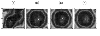
その結果、フォトマスク用基板9の下面9cについては、図6に示すように、1次創成加工および仕上げ研磨加工が進むに伴って所定の曲率の凹面に近づくことが確認された。ここで、表示エリアD1には下面9cの現在形状と平面との差分に応じて異なる色を表示しているため、下面9cが所定の曲率の凹面となれば、表示エリアD1には、同心円状の配色が現れることが理解される。ここで加工前の状態では、図6(a)に示すように、所定の曲率の凹面に対応する同心円状の配色から乖離した不規則な配色がソフトウェアSの第1の表示エリアD1に表示されたのに対して、1次創成加工後の状態の一例を示す図6(b)、および仕上げ研磨加工後の状態の一例を示す図6(c)又は別の例を示す図6(d)では、所定の曲率の凹面に対応する同心円状の配色に近い配色がソフトウェアSの第1の表示エリアD1に表示された。
また、フォトマスク用基板9の上面9bについては、図7に示すように、1次創成加工および仕上げ研磨加工が進むに伴って所定の曲率の凸面に近づくことが確認された。すなわち、加工前の状態では、図7(a)に示すように、所定の曲率の凸面に対応する同心円状の配色から乖離した不規則な配色がソフトウェアSの第1の表示エリアD1に表示されたのに対して、1次創成加工後の状態の一例を示す図7(b)、および仕上げ研磨加工後の状態の一例を示す図7(c)又は別の例を示す図7(d)では、所定の曲率の凸面に対応する同心円状の配色に近い配色がソフトウェアSの第1の表示エリアD1に表示された。
このフォトマスク用基板9の下面9cおよび上面9bの平面度の推移を細かく示したのが、図8の折れ線グラフである。この折れ線グラフにおいて、横軸は時間(加工の回数)を表し、縦軸は平面度(単位:μm)を表す。この折れ線グラフから明らかなように、フォトマスク用基板9では、下面9c、上面9bとも、1次創成加工を繰り返すうちに、平面度が目標値の30μmに近づき、仕上げ研磨加工により、その目標値がほぼ維持される傾向が認められた。
<変形例>
なお、上述した実施例1では、フォトマスク1を製造する際に、下面荷重分布決定工程(ステップS3)および上面荷重分布決定工程(ステップS9)において、第1の表示エリアD1に平面度のデータを表示する場合について説明した。しかし、この第1の表示エリアD1には、平面度のデータをそのまま表示する代わりに、例えば、上述のように、下面形状判定工程(ステップS6)および上面形状判定工程(ステップS12)で設定する目標値からそのデータを減じた値を表示してもよい。このようにすれば、実際には凹凸面に仕上げているにもかかわらず、ソフトウェアS上では平坦に仕上げる通常の研磨と同じように表示されるため、凹凸面に仕上げるからといって、作業者が混乱して作業に迷いが生じる事態を回避することが可能となる。
なお、上述した実施例1では、フォトマスク1を製造する際に、下面荷重分布決定工程(ステップS3)および上面荷重分布決定工程(ステップS9)において、第1の表示エリアD1に平面度のデータを表示する場合について説明した。しかし、この第1の表示エリアD1には、平面度のデータをそのまま表示する代わりに、例えば、上述のように、下面形状判定工程(ステップS6)および上面形状判定工程(ステップS12)で設定する目標値からそのデータを減じた値を表示してもよい。このようにすれば、実際には凹凸面に仕上げているにもかかわらず、ソフトウェアS上では平坦に仕上げる通常の研磨と同じように表示されるため、凹凸面に仕上げるからといって、作業者が混乱して作業に迷いが生じる事態を回避することが可能となる。
[発明の実施の形態2]
次に、実施の形態2として、実施の形態1のフォトマスク1を用いて感光基板Pを露光する方法について、図9を参照して説明する。
次に、実施の形態2として、実施の形態1のフォトマスク1を用いて感光基板Pを露光する方法について、図9を参照して説明する。
フォトマスク1(図1)は、一例として、実施の形態1の光学素子の製造方法を用いて、下面9cが所定の曲率の凹面に形成され、上面9bが所定の曲率の凸面に形成されたフォトマスク用基板9に対して、クロム成膜、レジスト塗布、露光・現像、クロム膜エッチング、レジスト剥離、欠陥修正、ペリクル貼付等の処理を施すことにより得られる。このようにして得られたフォトマスク1は、一例として下面1cに回路パターン等の所定のパターンが形成されている。
上記の処理はフォトマスク用基板9(図3)を周縁部9aにおいて支持し、下面9c、上面9bが水平方向に延在するように配置した状態で行うことができる。この時、フォトマスク用基板9は自重により中心部9d近傍が下垂し、下面9c、上面9bは共に平面(水平面)となる。よって本実施形態においては、フォトマスク用基板9に対するクロム成膜、レジスト塗布、露光・現像等の上記の処理を、フォトマスク用基板9のたわみによる形状変化の影響を受けることなく、好適な状態で行うことができる。
次に、上記の工程により製造されたフォトマスク1を図9に概略的な構成を示す露光装置2に載置して露光光ELを照射し、フォトマスク1に形成された回路パターン等を感光基板P等の上に投影露光する。
露光装置2は、図9に示す通り、フォトマスク1を支持するマスクステージMSTと、感光基板Pを支持する基板ステージPSTと、マスクステージMSTに支持されているフォトマスク1を露光光ELで照明する照明光学系ILと、露光光ELで照明されたフォトマスク1の回路パターン等を基板ステージPSTに支持されている感光基板Pに投影露光する投影光学系PLとを備えている。マスクステージMSTは投影光学系PLの物体面側においてフォトマスク1を支持し、基板ステージPSTは、投影光学系PLの像面側において感光基板Pを支持する。本実施形態において、照明光学系ILは複数(5つ)の照明系モジュール(不図示)により構成されており、投影光学系PLも、照明系モジュールの数に対応して複数(5つ)の投影光学系PLa~PLeを有している。投影光学系PLa~PLeのそれぞれは、5つの照明系モジュールのそれぞれに対応して配置されている。上記の構成により、本実施形態に係る露光装置2においては、この投影光学系PLに対してフォトマスク1と感光基板Pとを所定方向に同期移動しつつフォトマスク1を露光光ELで照明し、フォトマスク1の下面1cに形成された回路パターン等が感光基板Pに露光される。すなわち本実施形態に係る露光装置2は、いわゆるマルチレンズスキャン型露光装置である。
ここで、フォトマスク1は、下面9cが所定の曲率の凹面に形成され、上面9bが所定の曲率の凸面に形成されたフォトマスク用基板9(図3)を用いて形成されているため、マスクステージMSTにおいて、パターン面(下面1c)と上面1bが共に平面(水平面)となるように配置される。したがって、フォトマスク1を用いた露光方法においては、フォトマスク1のたわみに起因する結像性能の劣化が防止されている。
なお、図9に示す露光装置2はマルチレンズスキャン型露光装置であるが、露光装置は、投影光学系を1つ有し、フォトマスク1と感光基板Pを同期移動してフォトマスク1のパターンを露光するスキャン型露光装置であってもよく、フォトマスク1と感光基板Pとを静止した状態でフォトマスク1のパターンを露光し、感光基板Pを順次ステップ移動させるステップ・アンド・リピート型の露光装置にも適用することができる。
本国際出願は、2012年8月9日に出願した日本国特許出願第2012-177096号に基づく優先権を主張するものであり、日本国特許出願第2012-177096号の全内容を本国際出願に援用する。
本発明は、露光装置に使用するフォトマスクなどの光学素子を製造する際に広く適用することができる。また、製造した光学素子を用いた露光方法においても広く適用することができる。
1……フォトマスク(光学素子)
1a……周縁部
1b……上面
1c……下面
1d……中心部
2……露光装置
5……機体
6……キャリア
6a……ガイド孔
7……下定盤
7a……研磨面
8……片面研磨装置(研磨手段)
9……フォトマスク用基板(光学素子用基板)
9a……周縁部
9b……上面
9c……下面
9d……中心部
A、A1、A2、A3……載荷領域
IL……照明光学系
MST……マスクステージ
P……感光基板
PL……投影光学系
PST……基板ステージ
W……重り(荷重)
1a……周縁部
1b……上面
1c……下面
1d……中心部
2……露光装置
5……機体
6……キャリア
6a……ガイド孔
7……下定盤
7a……研磨面
8……片面研磨装置(研磨手段)
9……フォトマスク用基板(光学素子用基板)
9a……周縁部
9b……上面
9c……下面
9d……中心部
A、A1、A2、A3……載荷領域
IL……照明光学系
MST……マスクステージ
P……感光基板
PL……投影光学系
PST……基板ステージ
W……重り(荷重)
Claims (11)
- 光学素子用基板の両面を創成加工して成形する光学素子の製造方法であって、
前記光学素子用基板は、周縁部が支持されて略水平に配置され、自重によって中心部付近が下垂した状態となった場合において前記両面がほぼ平面になるように、前記周縁部が支持されて略水平に配置される前の状態で一方の面が所定の凸面になるとともに、他方の面が所定の凹面になるように創成加工され、
前記創成加工は、
前記光学素子用基板の前記所定の凸面および前記所定の凹面の形状を算出する目標形状算出工程と、
自重によって中心部付近が下垂していない状態における前記光学素子用基板の前記両面の形状を測定する形状測定工程と、
前記目標形状算出工程で算出された前記光学素子用基板の前記所定の凸面の形状と前記形状測定工程で測定された自重によって中心部付近が下垂していない状態における前記光学素子用基板の前記一方の面の形状との差に基づき、前記光学素子用基板の複数の載荷領域に作用させる荷重の分布を決定し、かつ前記目標形状算出工程で算出された前記光学素子用基板の前記所定の凹面の形状と前記形状測定工程で測定された自重によって中心部付近が下垂していない状態における前記光学素子用基板の前記他方の面の形状との差に基づき前記光学素子用基板の複数の載荷領域に作用させる荷重の分布を決定する荷重分布決定工程と、
研磨手段の研磨面の上側に前記光学素子用基板を載置し、前記荷重分布決定工程で決定された荷重の分布に従って前記載荷領域に荷重を作用させた状態で、前記光学素子用基板に対して前記研磨面を相対移動させることにより、当該光学素子用基板の前記一方の面または前記他方の面を創成加工する基板創成加工工程と、
前記基板創成加工工程で創成加工された前記光学素子用基板の前記一方の面の形状と前記目標形状算出工程で算出された前記光学素子用基板の前記所定の凸面の形状との差、または前記基板創成加工工程で創成加工された前記光学素子用基板の前記他方の面の形状と前記目標形状算出工程で算出された前記光学素子用基板の前記所定の凹面の形状との差が所定の許容範囲に入れば加工を終了する形状判定工程とを含む光学素子の製造方法。 - 前記所定の凸面は所定の曲率の凸面であり、前記所定の凹面は所定の曲率の凹面である請求項1に記載の光学素子の製造方法。
- 光学素子用基板の両面を創成加工して成形する光学素子の製造方法であって、
前記光学素子用基板は、周縁部が支持されて略水平に配置され、自重によって中心部付近が下垂した状態となった場合において前記両面がほぼ平面になるように、前記周縁部が支持されて略水平に配置される前の状態で一方の面が所定の凸面になるとともに、他方の面が所定の凹面になるように創成加工され、
前記創成加工は、
前記光学素子用基板の前記所定の凸面および前記所定の凹面の形状を算出する目標形状算出工程と、
自重によって中心部付近が下垂していない状態における前記光学素子用基板の前記両面の形状を測定する形状測定工程と、
前記目標形状算出工程で算出された前記光学素子用基板の前記所定の凸面の形状と前記形状測定工程で測定された自重によって中心部付近が下垂していない状態における前記光学素子用基板の前記一方の面の形状との差に基づき、前記光学素子用基板の複数の載荷領域に作用させる荷重の分布を決定し、かつ前記目標形状算出工程で算出された前記光学素子用基板の前記所定の凹面の形状と前記形状測定工程で測定された自重によって中心部付近が下垂していない状態における前記光学素子用基板の前記他方の面の形状との差に基づき前記光学素子用基板の複数の載荷領域に作用させる荷重の分布を決定する荷重分布決定工程と、
研磨手段の研磨面の上側に前記光学素子用基板を載置し、前記荷重分布決定工程で決定された荷重の分布に従って前記載荷領域に荷重を作用させた状態で、前記光学素子用基板に対して前記研磨面を相対移動させることにより、当該光学素子用基板の前記一方の面または前記他方の面のいずれか一方を創成加工する第1基板創成加工工程と、
前記第1基板創成加工工程で創成加工された前記光学素子用基板の前記一方の面または前記他方の面のいずれか一方の形状と、前記光学素子用基板の当該面に対応する前記目標形状算出工程で算出された前記光学素子用基板の前記所定の凸面または前記所定の凹面の形状との差が、所定の許容範囲に入れば、第1の加工を終了する第1形状判定工程と、
研磨手段の研磨面の上側に前記光学素子用基板を載置し、前記荷重分布決定工程で決定された荷重の分布に従って前記載荷領域に荷重を作用させた状態で、前記光学素子用基板に対して前記研磨面を相対移動させることにより、当該光学素子用基板の前記一方の面または前記他方の面の他方を創成加工する第2基板創成加工工程と、
前記第2基板創成加工工程で創成加工された前記光学素子用基板の前記一方の面または前記他方の面の他方の形状と、前記光学素子用基板の当該面に対応する前記目標形状算出工程で算出された前記光学素子用基板の前記所定の凸面または前記所定の凹面の形状との差が、所定の許容範囲に入れば、第2の加工を終了する第2形状判定工程とを含むことを特徴とする光学素子の製造方法。 - 前記所定の凸面は所定の曲率の凸面であり、前記所定の凹面は所定の曲率の凹面である請求項3に記載の光学素子の製造方法。
- 前記基板創成加工工程において、前記載荷領域に作用する荷重の大きさが前記光学素子用基板の中心部と周縁部とで異なるように、前記載荷領域に荷重を作用させる請求項1乃至4のいずれか一項に記載の光学素子の製造方法。
- 前記基板創成加工工程において、前記光学素子用基板の中心部の前記載荷領域に作用する前記荷重の大きさが、前記光学素子用基板の周縁部の前記載荷領域に作用する前記荷重の大きさよりも大きい請求項5に記載の光学素子の製造方法。
- 前記基板創成加工工程において、前記光学素子用基板の周縁部の前記載荷領域に作用する前記荷重の大きさが、前記光学素子用基板の中心部の前記載荷領域に作用する前記荷重の大きさよりも大きい請求項5に記載の光学素子の製造方法。
- 前記基板創成加工工程において、前記載荷領域に重りを載せることにより、当該載荷領域に荷重を作用させた状態で、前記光学素子用基板の前記一方の面又は前記他方の面を創成加工する請求項1乃至7のいずれか一項に記載の光学素子の製造方法。
- 前記光学素子用基板が矩形である請求項1乃至8のいずれか一項に記載の光学素子の製造方法
- 前記光学素子用基板がフォトマスク用基板である請求項1乃至9のいずれか一項に記載の光学素子の製造方法。
- 投影光学系を介してパターンの像を基板上に投影することにより前記基板を露光する露光方法であって、
前記投影光学系の物体面側に前記パターンを配置することと、
前記パターンに露光光を照射することとを含み、
前記パターンは、請求項1~10のいずれか一項に記載の製造方法により製造された光学素子に形成されている露光方法。
Priority Applications (1)
| Application Number | Priority Date | Filing Date | Title |
|---|---|---|---|
| KR20157002079A KR20150041621A (ko) | 2012-08-09 | 2013-08-09 | 광학 소자의 제조 방법, 및 이 광학 소자를 사용한 노광 방법 |
Applications Claiming Priority (2)
| Application Number | Priority Date | Filing Date | Title |
|---|---|---|---|
| JP2012177096A JP2014034497A (ja) | 2012-08-09 | 2012-08-09 | 光学素子の製造方法 |
| JP2012-177096 | 2012-08-09 |
Publications (1)
| Publication Number | Publication Date |
|---|---|
| WO2014025047A1 true WO2014025047A1 (ja) | 2014-02-13 |
Family
ID=50068263
Family Applications (1)
| Application Number | Title | Priority Date | Filing Date |
|---|---|---|---|
| PCT/JP2013/071727 Ceased WO2014025047A1 (ja) | 2012-08-09 | 2013-08-09 | 光学素子の製造方法、及びこの光学素子を用いた露光方法 |
Country Status (4)
| Country | Link |
|---|---|
| JP (1) | JP2014034497A (ja) |
| KR (1) | KR20150041621A (ja) |
| TW (1) | TWI612375B (ja) |
| WO (1) | WO2014025047A1 (ja) |
Citations (4)
| Publication number | Priority date | Publication date | Assignee | Title |
|---|---|---|---|---|
| JP2004029735A (ja) * | 2002-03-29 | 2004-01-29 | Hoya Corp | 電子デバイス用基板、該基板を用いたマスクブランクおよび転写用マスク、並びにこれらの製造方法、研磨装置および研磨方法 |
| JP2009508143A (ja) * | 2005-09-12 | 2009-02-26 | 旭硝子株式会社 | フォトマスク、フォトマスク製造方法、および、フォトマスク加工装置 |
| JP2010511203A (ja) * | 2006-11-29 | 2010-04-08 | コーニング インコーポレイテッド | 高アスペクト比ガラス品のサブアパーチャ確定的超精密仕上 |
| JP2011175240A (ja) * | 2010-01-29 | 2011-09-08 | Hoya Corp | マスクブランク用基板、マスクブランク、転写用マスク及び半導体デバイスの製造方法 |
Family Cites Families (7)
| Publication number | Priority date | Publication date | Assignee | Title |
|---|---|---|---|---|
| JP3975321B2 (ja) * | 2001-04-20 | 2007-09-12 | 信越化学工業株式会社 | フォトマスク用シリカガラス系基板及びフォトマスク用シリカガラス系基板の平坦化方法 |
| JP3572053B2 (ja) * | 2001-05-31 | 2004-09-29 | 株式会社東芝 | 露光マスクの製造方法、マスク基板情報生成方法、半導体装置の製造方法およびサーバー |
| JP3916627B2 (ja) * | 2001-09-28 | 2007-05-16 | Hoya株式会社 | マスクブランク及びその製造方法、並びにマスクの製造方法 |
| US6885436B1 (en) * | 2002-09-13 | 2005-04-26 | Lsi Logic Corporation | Optical error minimization in a semiconductor manufacturing apparatus |
| JP4029828B2 (ja) * | 2003-11-18 | 2008-01-09 | 凸版印刷株式会社 | 両面マスク用ブランクの製造方法および両面マスクの製造方法 |
| JP4697735B2 (ja) * | 2005-11-21 | 2011-06-08 | Hoya株式会社 | マスクブランク、マスクブランクの製造方法、及びマスクの製造方法 |
| JP2010204264A (ja) * | 2009-03-02 | 2010-09-16 | Dainippon Printing Co Ltd | 両面にパターンを有するフォトマスクの作製方法 |
-
2012
- 2012-08-09 JP JP2012177096A patent/JP2014034497A/ja active Pending
-
2013
- 2013-08-09 WO PCT/JP2013/071727 patent/WO2014025047A1/ja not_active Ceased
- 2013-08-09 KR KR20157002079A patent/KR20150041621A/ko not_active Ceased
- 2013-08-09 TW TW102128614A patent/TWI612375B/zh active
Patent Citations (4)
| Publication number | Priority date | Publication date | Assignee | Title |
|---|---|---|---|---|
| JP2004029735A (ja) * | 2002-03-29 | 2004-01-29 | Hoya Corp | 電子デバイス用基板、該基板を用いたマスクブランクおよび転写用マスク、並びにこれらの製造方法、研磨装置および研磨方法 |
| JP2009508143A (ja) * | 2005-09-12 | 2009-02-26 | 旭硝子株式会社 | フォトマスク、フォトマスク製造方法、および、フォトマスク加工装置 |
| JP2010511203A (ja) * | 2006-11-29 | 2010-04-08 | コーニング インコーポレイテッド | 高アスペクト比ガラス品のサブアパーチャ確定的超精密仕上 |
| JP2011175240A (ja) * | 2010-01-29 | 2011-09-08 | Hoya Corp | マスクブランク用基板、マスクブランク、転写用マスク及び半導体デバイスの製造方法 |
Also Published As
| Publication number | Publication date |
|---|---|
| TW201413372A (zh) | 2014-04-01 |
| JP2014034497A (ja) | 2014-02-24 |
| KR20150041621A (ko) | 2015-04-16 |
| TWI612375B (zh) | 2018-01-21 |
Similar Documents
| Publication | Publication Date | Title |
|---|---|---|
| KR101701771B1 (ko) | 마스크블랭크용 기판의 제조방법, 마스크블랭크의 제조방법, 전사용 마스크의 제조방법 및 반도체 디바이스의 제조방법 | |
| TW201937553A (zh) | 微影製程和設備及檢測製程和設備 | |
| JP6609694B2 (ja) | 基板ホルダ、リソグラフィ装置、及びデバイスを製造する方法 | |
| TW201405240A (zh) | 微影製程及使用於一微影系統之微影製程 | |
| TW201935138A (zh) | 用於控制製造設備的方法及相關設備 | |
| KR20190114787A (ko) | 리소그래피 장치, 패턴 형성 방법, 및 물품 제조 방법 | |
| JP2013055157A (ja) | インプリント装置及び物品の製造方法 | |
| US20190294059A1 (en) | Method of determining pellicle compensation corrections for a lithographic process, metrology apparatus and computer program | |
| JP2024049249A (ja) | 原版、情報処理装置、リソグラフィ装置及び物品の製造方法 | |
| TWI705293B (zh) | 光罩之製造方法、描繪裝置、顯示裝置之製造方法、光罩基板之檢查方法、及光罩基板之檢查裝置 | |
| TWI752604B (zh) | 微影製程之子場控制及其相關設備 | |
| JP2011508960A (ja) | リソグラフィ装置及び方法 | |
| CN106707691A (zh) | 曝光装置及方法 | |
| JP7596106B2 (ja) | 情報処理装置、検査方法、プログラム、露光装置、決定方法、及び物品の製造方法 | |
| CN110244518B (zh) | 决定方法、曝光方法、装置、物品的制造方法及存储介质 | |
| JP7330777B2 (ja) | ステージ装置、制御方法、基板処理装置、および物品の製造方法 | |
| JP2019200444A (ja) | リソグラフィ装置、パターン形成方法及び物品の製造方法 | |
| TWI612375B (zh) | 光學元件之製造方法、及使用該光學元件之曝光方法 | |
| JP2021005047A (ja) | 露光装置、露光方法、および物品の製造方法 | |
| JP7330778B2 (ja) | ステージ装置、制御方法、基板処理装置、および物品の製造方法 | |
| CN108292111A (zh) | 用于在光刻设备中处理衬底的方法和设备 | |
| US20230341782A1 (en) | Lithography information processing apparatus, lithography system, storage medium, lithography information processing method, and article manufacturing method | |
| TW201602735A (zh) | 微影設備及方法 | |
| JP6071263B2 (ja) | 露光装置、露光システム、それらを用いたデバイスの製造方法 | |
| TW202613728A (zh) | 用於對基板區域上之度量衡資料模型化之方法及相關設備 |
Legal Events
| Date | Code | Title | Description |
|---|---|---|---|
| 121 | Ep: the epo has been informed by wipo that ep was designated in this application |
Ref document number: 13827931 Country of ref document: EP Kind code of ref document: A1 |
|
| ENP | Entry into the national phase |
Ref document number: 20157002079 Country of ref document: KR Kind code of ref document: A |
|
| NENP | Non-entry into the national phase |
Ref country code: DE |
|
| 122 | Ep: pct application non-entry in european phase |
Ref document number: 13827931 Country of ref document: EP Kind code of ref document: A1 |