WO2014017240A1 - センサ装置 - Google Patents
センサ装置 Download PDFInfo
- Publication number
- WO2014017240A1 WO2014017240A1 PCT/JP2013/067431 JP2013067431W WO2014017240A1 WO 2014017240 A1 WO2014017240 A1 WO 2014017240A1 JP 2013067431 W JP2013067431 W JP 2013067431W WO 2014017240 A1 WO2014017240 A1 WO 2014017240A1
- Authority
- WO
- WIPO (PCT)
- Prior art keywords
- sensor device
- power supply
- output
- voltage
- electrode
- Prior art date
- Legal status (The legal status is an assumption and is not a legal conclusion. Google has not performed a legal analysis and makes no representation as to the accuracy of the status listed.)
- Ceased
Links
Images


Classifications
-
- G—PHYSICS
- G01—MEASURING; TESTING
- G01R—MEASURING ELECTRIC VARIABLES; MEASURING MAGNETIC VARIABLES
- G01R19/00—Arrangements for measuring currents or voltages or for indicating presence or sign thereof
- G01R19/165—Indicating that current or voltage is either above or below a predetermined value or within or outside a predetermined range of values
- G01R19/16533—Indicating that current or voltage is either above or below a predetermined value or within or outside a predetermined range of values characterised by the application
- G01R19/16538—Indicating that current or voltage is either above or below a predetermined value or within or outside a predetermined range of values characterised by the application in AC or DC supplies
-
- G—PHYSICS
- G01—MEASURING; TESTING
- G01L—MEASURING FORCE, STRESS, TORQUE, WORK, MECHANICAL POWER, MECHANICAL EFFICIENCY, OR FLUID PRESSURE
- G01L19/00—Details of, or accessories for, apparatus for measuring steady or quasi-steady pressure of a fluent medium insofar as such details or accessories are not special to particular types of pressure gauges
- G01L19/08—Means for indicating or recording, e.g. for remote indication
- G01L19/12—Alarms or signals
-
- G—PHYSICS
- G01—MEASURING; TESTING
- G01L—MEASURING FORCE, STRESS, TORQUE, WORK, MECHANICAL POWER, MECHANICAL EFFICIENCY, OR FLUID PRESSURE
- G01L27/00—Testing or calibrating of apparatus for measuring fluid pressure
- G01L27/007—Malfunction diagnosis, i.e. diagnosing a sensor defect
-
- G—PHYSICS
- G01—MEASURING; TESTING
- G01L—MEASURING FORCE, STRESS, TORQUE, WORK, MECHANICAL POWER, MECHANICAL EFFICIENCY, OR FLUID PRESSURE
- G01L9/00—Measuring steady of quasi-steady pressure of fluid or fluent solid material by electric or magnetic pressure-sensitive elements; Transmitting or indicating the displacement of mechanical pressure-sensitive elements, used to measure the steady or quasi-steady pressure of a fluid or fluent solid material, by electric or magnetic means
-
- G—PHYSICS
- G01—MEASURING; TESTING
- G01R—MEASURING ELECTRIC VARIABLES; MEASURING MAGNETIC VARIABLES
- G01R19/00—Arrangements for measuring currents or voltages or for indicating presence or sign thereof
- G01R19/165—Indicating that current or voltage is either above or below a predetermined value or within or outside a predetermined range of values
-
- G—PHYSICS
- G01—MEASURING; TESTING
- G01R—MEASURING ELECTRIC VARIABLES; MEASURING MAGNETIC VARIABLES
- G01R31/00—Arrangements for testing electric properties; Arrangements for locating electric faults; Arrangements for electrical testing characterised by what is being tested not provided for elsewhere
- G01R31/28—Testing of electronic circuits, e.g. by signal tracer
- G01R31/282—Testing of electronic circuits specially adapted for particular applications not provided for elsewhere
- G01R31/2829—Testing of circuits in sensor or actuator systems
Definitions
- the present invention relates to a sensor device, and more particularly to a sensor device that fixes an output voltage to a power supply voltage or a ground potential when the power supply is disconnected.
- Patent Document 1 Japanese Patent Application Laid-Open No. 2004-294069
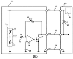
- FIG. 3 shows a configuration when the above-described conventional technology is applied to a resistance type detection element.
- power is supplied from the control device 40 to the sensor device 28 via the power supply line 37 and the ground line 39, and the sensor output voltage is sent to the control device 40 via the output line 38.
- the control device 40 is provided with a constant voltage source 41 for supplying a constant voltage to the sensor device 28 and a pull-up resistor 42 connected between the output line 38 and the constant voltage source 41.
- the sensor device 28 includes a resistance type detection element 29, and includes resistors 30 and 31 whose resistance values change according to the detected physical quantity, and the voltage Vsen changes according to the detected physical quantity.
- the voltage Vsen is amplified by an output circuit including resistors 32 and 33, an amplifier 34, a reference power supply 35, and an output transistor 36, and is output to the control device 40 via an output terminal Vout and an output line 38.
- the voltage at the output terminal Vout is determined by the divided voltage by the resistors 31, 32, 33 and the pull-up resistor 42. That is, the voltage of the output terminal Vout is not fixed to the power supply voltage or the ground potential, but becomes an intermediate potential (a voltage range output when the sensor device is normal).
- the control device 40 when the voltage of the output terminal Vout is fixed to the power supply voltage or the ground potential, it can be determined that the sensor device 28 has failed.
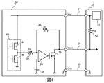
- FIG. 4 shows a configuration in the case where the CMOS amplifier circuit 43 is connected to the previous stage of the configuration shown in FIG. FIG. 4 shows only the PMOS transistor 44 and the NMOS transistor 45 at the output stage with respect to the internal configuration of the CMOS amplifier circuit 43.
- the voltage of the constant voltage source 41 is supplied from the drain electrode of the pull-up resistor 42, resistor 33, resistor 32, and PMOS transistor 44 to the power supply terminal Vcc via the well electrode. Then, power is supplied to the sensor device 28.
- the present invention has been made in view of the above circumstances, and an object thereof is to provide a sensor device that can reliably fix the output voltage of the sensor device to a power supply voltage or a ground potential when the power supply line is disconnected.
- the present invention has arranged a series circuit of a MOS switch and a capacitor in the negative feedback portion of the output circuit for generating the sensor output voltage, and connected an element acting as a diode to the well electrode of the MOS switch. Is.
- the output voltage of the sensor device can be reliably fixed to the power supply or ground potential. For this reason, since it becomes possible to detect a failure of the sensor device in the control device using the sensor device, it is possible to ensure fail-safety of the control system using the sensor device.
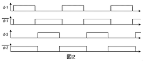
- Circuit configuration of sensor device of first embodiment Timing chart of clock signals ⁇ 1, ⁇ 2 Configuration when conventional technology is applied to a resistance type sensing element Configuration when CMOS amplifier circuit 43 is connected to the previous stage of the configuration shown in FIG.
- Circuit configuration of sensor device of second embodiment Cross-sectional structure of the PMOS transistor 46 Circuit configuration of sensor device of third embodiment Circuit configuration of sensor device of fourth embodiment Circuit configuration of sensor device of fifth embodiment
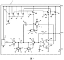
- FIGS. 1 is a circuit configuration of the sensor device of the first embodiment
- FIG. 2 is a timing chart of the clock signals ⁇ 1 and ⁇ 2.
- the control device 25 In the sensor device 1 of this embodiment, power is supplied from the control device 25 to the power supply terminal Vcc and the ground terminal Gnd of the sensor device 1 through the power supply line 22 and the ground line 24, and from the output terminal Vout to the sensor via the output line 23.
- the output voltage is sent to the control device 25.
- the control device 25 includes a constant voltage source 26 that supplies a constant voltage to the sensor device 1, and a pull-up resistor 27 that is connected between the output line 23 and the constant voltage source 26.
- a detection element 8 is arranged in the sensor device 1, and the voltage Vsen changes according to the detected physical quantity.
- a pressure sensor, an acceleration sensor, an angular velocity sensor, an air flow sensor, or the like is used for the detection element 8.
- An output circuit composed of an operational amplifier 19, a reference voltage source 20, and an SWC (switched capacitor) circuit composed of an output NMOS transistor 21 amplifies the voltage Vsen and outputs an output terminal Vout and an output line 23.
- a series circuit of the MOS switch 4 and the capacitor 2 is provided in the negative feedback portion, and the well electrode of the MOS switch 4 is connected to the power supply terminal Vcc via the diode 3.
- the well electrode of the MOS switch 7 was also connected to the power supply terminal Vcc via the diode 3.
- the current path flowing from the output terminal Vout to the capacitor 2 via the MOS switches 4 and 5 is interrupted by the capacitor 2.
- the current path flowing from the output terminal Vout to the drain (source) electrode of the MOS switch 4, the well electrode of the MOS switch 4, and the power supply terminal Vcc via the diode 3 is the diode 3 is connected to the well electrode of the MOS switch 4 from the power supply terminal Vcc. Since the direction is the forward direction, the diode 3 is in the reverse direction from the well electrode of the MOS switch 4 toward the power supply terminal Vcc, so that the current is cut off.
- the current path flowing from the output terminal Vout through the capacitor 18 is interrupted by the capacitor 18.
- the current path that flows from the output terminal Vout to the power supply terminal Vcc from the well electrode of the MOS switch 7 through the MOS switches 4 and 5 to the power supply terminal Vcc is cut off, so that the current is cut off.
- the current path flowing from the output terminal Vout to the ground terminal Gnd from the MOS switches 6 and 7 through the MOS switches 4 and 5 is controlled by the clock signals ⁇ 1 and ⁇ 2 shown in FIG.
- the current is cut off.
- the voltages of the clock signals ⁇ 1 and ⁇ 2 may be unstable. In this case, the current can be reliably cut off by deleting the MOS switch 7.
- the control device 25 can determine that some failure has occurred in the sensor device 1, can take a countermeasure corresponding to this failure, and can operate in a fail-safe manner as a control system using the sensor device 1. it can.
- the configuration of the output circuit is an open drain type circuit configuration by the output MOS transistor 21.
- the PMOS transistor can be eliminated from the output transistor.
- the well electrode of the PMOS transistor is connected to the power supply terminal Vcc.
- the power supply line 22 is disconnected, a current will flow from the constant voltage source 26 to the power supply terminal Vcc via the pull-up resistor 27 and the output terminal Vout. A current path is generated. Since the PMOS transistor used as the output transistor performs an analog operation, it is very difficult to eliminate a current path from the output terminal Vout to the power supply terminal Vcc without impairing the analog operation.
- FIGS. 5 shows the circuit configuration of the sensor device of the second embodiment
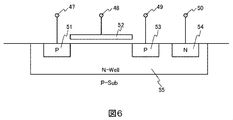
- FIG. 6 shows the cross-sectional structure of the PMOS transistor 46.
- the sensor device of the second embodiment has basically the same configuration as the sensor device of the first embodiment, but the following improvements have been made.
- a PMOS transistor 46 is provided instead of the diode 3
- the source electrode 47 of the PMOS transistor 46 is connected to the power supply terminal Vcc
- the drain electrode 49, the well electrode 50 and the gate electrode 48 are connected to the well electrodes of the MOS switches 4 and 7. did.
- the diode element and the MOS transistor are arranged substantially in parallel between the power supply terminal Vcc and the well electrodes of the MOS switches 4 and 7.
- a more stable potential can be supplied to the well electrodes of the MOS switches 4 and 7 when the power is normally supplied to the power supply terminal Vcc.
- the cross-sectional structure of the PMOS transistor 46 is shown in FIG.
- the PMOS transistor 46 is provided with an N-well region 55 (N-Well) on a P-type substrate (P-Sub), and P-type regions 51 and 53 are provided on the N-well region 55 (N-Well).
- a gate 52 is arranged between the source region and the drain region.
- a source electrode 47 is provided in the P-type region 51
- a drain electrode 49 is provided in the P-type region 53
- a gate electrode 48 is provided in the gate 52.
- An N-type region 54 is provided in the N-well region 55 (N-Well), and the well electrode 50 is disposed.
- the source electrode 47 of the PMOS transistor 46 is connected to the power supply terminal Vcc, and the drain electrode 49, the well electrode 50, and the gate electrode 48 are connected to the well electrodes of the MOS switches 4 and 7.
- a diode element having a PN junction formed by the P-type region 51 and the N-well region 55 is provided between the power supply terminal Vcc and the well electrodes of the MOS switches 4 and 7. Since the gate electrode 48 of the PMOS transistor 46 is connected to the well electrode side of the MOS switches 4 and 7, the potential of the gate electrode 48 of the PMOS transistor 46 is low when the potential of the well electrode of the MOS switches 4 and 7 is low. Therefore, the PMOS transistor 46 is turned on to raise the potential of the well electrodes of the MOS switches 4 and 7. Due to this effect, the potential of the gate electrode 48 of the PMOS transistor 46 can be stabilized at a higher speed.
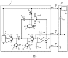
- FIG. 7 shows the circuit configuration of the sensor device of the third embodiment.
- the sensor device of the third embodiment has basically the same structure as the sensor device of the first embodiment, but the following improvements have been made.
- the resistor 56 and the MOS transistor 57 for reducing the voltage between the power supply terminal Vcc and the ground terminal Gnd to a predetermined voltage
- the power supply terminal Vcc and the ground terminal Gnd MOS transistors 58, 59, and 60 that are turned on and off according to the voltage between them
- MOS transistors 62, 64, and 66 that are controlled by turning on and off the MOS transistors 58, 59, and 60, and drain electrodes of the MOS transistors 62, 64, and 66
- Resistors 61, 63, and 65 disposed between the gate electrode and the output PMOS transistor 68 and the output NMOS transistor 69 that drive the voltage of the output terminal Vout, and the output PMOS transistor 68 and the output NMOS transistor 69 are controlled.
- Operational amplifier 67 Digits.
- the voltage between the power supply terminal Vcc and the ground terminal Gnd is lowered to a predetermined voltage by the resistor 56 and the MOS transistor 57.
- the MOS transistors 58, 59, 60 are connected when the voltage between the power supply terminal Vcc and the ground terminal Gnd is normal because the gate electrode is connected to the power supply terminal Vcc and the source electrode is connected to one end of the resistor 56.
- the power supply terminal Vcc is turned off, so that it functions as voltage detection means for detecting that the voltage between the power supply terminal Vcc and the ground terminal Gnd is lowered.
- the MOS transistors 62, 64, 66 are turned on when the MOS transistors 58, 59, 60 are on, the well electrodes of the MOS switches 4, 7, the source electrode and the well electrode of the output PMOS transistor 68 are connected to the power supply terminal Vcc. So that the voltage at the output terminal Vout is normally output. Since the MOS transistor 64 is connected in series with the output PMOS transistor 68, the output amplitude is reduced unless the size of the MOS transistor 64 is made sufficiently large. On the contrary, when the power supply terminal Vcc is opened and the MOS transistors 58, 59, 60 are turned off, the MOS transistors 62, 64, 66 are turned off.
- the source electrode and well electrode of the output PMOS transistor 68 are cut off from the power supply terminal Vcc. Since the well electrodes of the MOS transistors 62, 64, 66 are connected to the drain electrodes of the MOS transistors 62, 64, 66, the MOS transistor 62 has the well electrodes of the MOS transistors 4, 7 forward from the power supply terminal Vcc. Is connected to the MOS transistor 64. A diode element is connected to the MOS transistor 64 from the power supply terminal Vcc to the source electrode of the output PMOS transistor 68. The MOS transistor 66 is connected to the well of the output PMOS transistor 68 from the power supply terminal Vcc. A diode element having an electrode in the forward direction is connected.
- the control device 25 can determine that some failure has occurred in the sensor device 1, can take a countermeasure corresponding to this failure, and can operate in a fail-safe manner as a control system using the sensor device 1. it can.
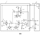
- FIG. 8 shows the circuit configuration of the sensor device of the fourth embodiment.
- the sensor device of the fourth embodiment has basically the same structure as the sensor device of the first embodiment, but the following improvements have been made.
- a CMOS process using a P-type substrate is assumed, but in this embodiment, a CMOS process using an N-type substrate is assumed.
- a pull-down resistor 72 is disposed at the output terminal Vout. Since the pull-down resistor 72 is used, an output PMOS transistor 71 is provided in the output circuit.
- the diode 70 is also arranged so that the direction from the MOS switches 5 and 6 to the ground terminal Gnd is the forward direction.
- FIG. 9 shows the circuit configuration of the sensor device of the fifth embodiment.
- the sensor device of the fifth embodiment has basically the same configuration as the sensor device of the fourth embodiment, but the following improvements have been made.
- an NMOS transistor 73 is provided instead of the diode 70, the source electrode of the NMOS transistor 73 is connected to the ground terminal Gnd, and the drain electrode, the well electrode, and the gate electrode are connected to the well electrodes of the MOS switches 5 and 6.
- the diode element and the MOS transistor are arranged substantially in parallel between the ground terminal Gnd and the well electrodes of the MOS switches 5 and 6.
- a stable potential can be supplied from the well electrodes of the MOS switches 5 and 6 when the power is normally supplied to the ground terminal Gnd.
- MOS transistor 67 Operational amplifier 68 68 Output PMOS transistor 69 ... output NMOS transistor, 70 ... diode, 71 ... output PMOS transistor, 72 ... pull-down resistor, 73 ... NMOS transistor.
Landscapes
- Physics & Mathematics (AREA)
- General Physics & Mathematics (AREA)
- Engineering & Computer Science (AREA)
- General Engineering & Computer Science (AREA)
- Electromagnetism (AREA)
- Biomedical Technology (AREA)
- Analytical Chemistry (AREA)
- Chemical & Material Sciences (AREA)
- Health & Medical Sciences (AREA)
- Power Engineering (AREA)
- Electronic Switches (AREA)
- Semiconductor Integrated Circuits (AREA)
- Measuring Fluid Pressure (AREA)
- Transmission And Conversion Of Sensor Element Output (AREA)
- Measurement Of Current Or Voltage (AREA)
Abstract
Description
Claims (8)
- 所定の物理量を検出するセンサ装置であって、外部から電源を供給される電源端子およびグランド端子と、前記センサ装置の出力信号を外部へアナログ電圧として出力する出力端子と、前記出力端子の出力信号を生成する出力回路とを有するセンサ装置において、
前記出力回路の負帰還部に配置したMOSスイッチとコンデンサとの直列回路と、
前記MOSスイッチのウエル電極に接続したダイオードとして働く素子と、
を有することを特徴とするセンサ装置。 - 請求項1に記載のセンサ装置において、
前記出力回路はオープンドレイン型の出力回路であることを特徴とするセンサ装置。 - 請求項2に記載のセンサ装置において、
前記出力回路はNMOSのオープンドレイン回路であって、前記ダイオードとして働く素子は電源端子から前記MOSスイッチのウエル電極方向を順方向とすることを特徴とするセンサ装置。 - 請求項2に記載のセンサ装置において、
前記出力回路はPMOSのオープンドレイン回路であって、前記ダイオードとして働く素子は前記MOSスイッチのウエル電極からグランド端子方向を順方向とすることを特徴とするセンサ装置。 - 請求項1に記載のセンサ装置において、
前記電源端子あるいはグランド端子が開放した時に、前記電源端子と前記グランド端子との間の電圧を所定の電圧以下に低下させる手段と、前記電源端子と前記グランド端子との間の電圧が低下したことを検出する電圧検出手段と、前記電圧検出手段の出力に基づきオンオフする前記ダイオードとして働く素子と並列に接続されるMOSトランジスタと、を有することを特徴とするセンサ装置。 - 請求項3に記載のセンサ装置において、
前記ダイオードとして働く素子はPMOSトランジスタで構成され、
前記PMOSトランジスタのソース電極を電源端子に、ドレイン電極とウエル電極とゲート電極を前記MOSスイッチのウエル電極に接続したことを特徴とするセンサ装置。 - 請求項4に記載のセンサ装置において、
前記ダイオードとして働く素子はNMOSトランジスタで構成され、前記NMOSトランジスタのソース電極をグランド端子に、ドレイン電極とウエル電極とゲート電極を前記MOSスイッチのウエル電極に接続したことを特徴とするセンサ装置。 - 請求項1に記載のセンサ装置において、
前記電源端子あるいはグランド端子が開放時に、前記電源端子と前記グランド端子間の電圧を所定の電圧以下に低下させる手段と、前記電源端子と前記グランド端子間の電圧が低下したことを検出する電圧検出手段と、前記出力端子の電圧を制御するトランジスタと、前記出力端子の電圧を制御するトランジスタのウエル電極に前記電圧検出手段の出力に基づきオンオフ動作するトランジスタを接続したことを特徴とするセンサ装置。
Priority Applications (3)
| Application Number | Priority Date | Filing Date | Title |
|---|---|---|---|
| DE112013003667.3T DE112013003667B4 (de) | 2012-07-25 | 2013-06-26 | Sensorvorrichtung |
| US14/416,306 US9551735B2 (en) | 2012-07-25 | 2013-06-26 | Sensor device with series circuit of MOS switch and capacitor |
| CN201380039276.4A CN104487806B (zh) | 2012-07-25 | 2013-06-26 | 传感器件 |
Applications Claiming Priority (2)
| Application Number | Priority Date | Filing Date | Title |
|---|---|---|---|
| JP2012164295A JP5768016B2 (ja) | 2012-07-25 | 2012-07-25 | センサ装置 |
| JP2012-164295 | 2012-07-25 |
Publications (1)
| Publication Number | Publication Date |
|---|---|
| WO2014017240A1 true WO2014017240A1 (ja) | 2014-01-30 |
Family
ID=49997057
Family Applications (1)
| Application Number | Title | Priority Date | Filing Date |
|---|---|---|---|
| PCT/JP2013/067431 Ceased WO2014017240A1 (ja) | 2012-07-25 | 2013-06-26 | センサ装置 |
Country Status (5)
| Country | Link |
|---|---|
| US (1) | US9551735B2 (ja) |
| JP (1) | JP5768016B2 (ja) |
| CN (1) | CN104487806B (ja) |
| DE (1) | DE112013003667B4 (ja) |
| WO (1) | WO2014017240A1 (ja) |
Cited By (1)
| Publication number | Priority date | Publication date | Assignee | Title |
|---|---|---|---|---|
| CN113655267A (zh) * | 2021-04-12 | 2021-11-16 | 重庆大学 | 一种零角偏差测量的球面六电极式过电压传感器 |
Families Citing this family (8)
| Publication number | Priority date | Publication date | Assignee | Title |
|---|---|---|---|---|
| JP6581443B2 (ja) * | 2015-09-04 | 2019-09-25 | 日立オートモティブシステムズ株式会社 | センサ装置 |
| JP6585827B2 (ja) * | 2016-03-31 | 2019-10-02 | 日立オートモティブシステムズ株式会社 | センサ装置 |
| CN109960240A (zh) * | 2017-12-26 | 2019-07-02 | 宁波菲仕电机技术有限公司 | 基于mcu模拟量接口接线的断线检测装置及方法 |
| KR20200078992A (ko) * | 2018-12-24 | 2020-07-02 | (주)엘센 | 압력센서를 이용한 스마트 센싱시스템 |
| JP7403238B2 (ja) * | 2019-05-31 | 2023-12-22 | 日立Astemo株式会社 | 電子回路およびセンサシステム |
| CN111624518B (zh) * | 2020-05-25 | 2022-11-25 | 南京英锐创电子科技有限公司 | 传感器及其断路检测电路 |
| US20230221146A1 (en) * | 2020-07-06 | 2023-07-13 | Jatco Ltd | Rotation sensor |
| CN115629337B (zh) * | 2022-11-10 | 2026-02-17 | 赛卓电子科技(上海)股份有限公司 | 一种供电断线检测系统及车辆系统 |
Citations (1)
| Publication number | Priority date | Publication date | Assignee | Title |
|---|---|---|---|---|
| JP2001165817A (ja) * | 1999-12-06 | 2001-06-22 | Yazaki Corp | 断線検出回路 |
Family Cites Families (9)
| Publication number | Priority date | Publication date | Assignee | Title |
|---|---|---|---|---|
| JPH1114663A (ja) | 1997-06-27 | 1999-01-22 | Mitsubishi Electric Corp | 物理量センサ |
| JP4103280B2 (ja) * | 1999-12-24 | 2008-06-18 | 株式会社デンソー | 力学量センサ装置 |
| JP4438222B2 (ja) * | 2000-12-06 | 2010-03-24 | 株式会社デンソー | 物理量検出装置 |
| JP4296811B2 (ja) * | 2003-03-25 | 2009-07-15 | 株式会社デンソー | 物理量センサ装置 |
| AU2003268647A1 (en) * | 2003-09-18 | 2005-04-11 | Hitachi Car Engineering Co., Ltd. | Backup circuit |
| JP4761080B2 (ja) | 2008-02-01 | 2011-08-31 | Tdk株式会社 | 電流センサと電子制御ユニットとの間の断線検知システム |
| JP5305325B2 (ja) * | 2008-03-29 | 2013-10-02 | 新電元工業株式会社 | 異常検出保護回路及び方法、プログラム |
| DE102009020431A1 (de) | 2008-05-13 | 2009-11-19 | Continental Teves Ag & Co. Ohg | Sensoreinrichtung und Fehlererkennungsverfahren für elektronische Schaltungen in Kraftfahrzeugen |
| JP5517777B2 (ja) | 2010-06-25 | 2014-06-11 | 日立オートモティブシステムズ株式会社 | ブリッジ回路の断線検出回路および断線検出手段を有するシステム |
-
2012
- 2012-07-25 JP JP2012164295A patent/JP5768016B2/ja active Active
-
2013
- 2013-06-26 WO PCT/JP2013/067431 patent/WO2014017240A1/ja not_active Ceased
- 2013-06-26 DE DE112013003667.3T patent/DE112013003667B4/de active Active
- 2013-06-26 CN CN201380039276.4A patent/CN104487806B/zh active Active
- 2013-06-26 US US14/416,306 patent/US9551735B2/en active Active
Patent Citations (1)
| Publication number | Priority date | Publication date | Assignee | Title |
|---|---|---|---|---|
| JP2001165817A (ja) * | 1999-12-06 | 2001-06-22 | Yazaki Corp | 断線検出回路 |
Cited By (2)
| Publication number | Priority date | Publication date | Assignee | Title |
|---|---|---|---|---|
| CN113655267A (zh) * | 2021-04-12 | 2021-11-16 | 重庆大学 | 一种零角偏差测量的球面六电极式过电压传感器 |
| CN113655267B (zh) * | 2021-04-12 | 2023-09-12 | 重庆大学 | 一种零角偏差测量的球面六电极式过电压传感器 |
Also Published As
| Publication number | Publication date |
|---|---|
| DE112013003667B4 (de) | 2019-05-09 |
| JP2014025731A (ja) | 2014-02-06 |
| US20150260765A1 (en) | 2015-09-17 |
| DE112013003667T5 (de) | 2015-04-30 |
| US9551735B2 (en) | 2017-01-24 |
| CN104487806B (zh) | 2016-12-14 |
| JP5768016B2 (ja) | 2015-08-26 |
| CN104487806A (zh) | 2015-04-01 |
Similar Documents
| Publication | Publication Date | Title |
|---|---|---|
| JP5768016B2 (ja) | センサ装置 | |
| JP4890126B2 (ja) | ボルテージレギュレータ | |
| JP5547429B2 (ja) | 半導体装置 | |
| US7940036B2 (en) | Voltage comparison circuit, and semiconductor integrated circuit and electronic device having the same | |
| US10050031B2 (en) | Power conventer and semiconductor device | |
| JP6158682B2 (ja) | 磁気センサ回路 | |
| KR20190113551A (ko) | 볼티지 레귤레이터 | |
| US12047062B2 (en) | Electronic circuit and sensor system | |
| WO2017169057A1 (ja) | センサ装置 | |
| US6414521B1 (en) | Sense amplifier systems and methods | |
| KR100560260B1 (ko) | 바이어스 전압 발생 회로 및 차동 증폭 회로 | |
| US11929605B2 (en) | Semiconductor device | |
| TWI421508B (zh) | Power supply voltage reduction detection circuit | |
| JP6476049B2 (ja) | 温度センサ回路 | |
| US7724486B2 (en) | Sensing a current signal in an integrated circuit | |
| JP6332601B2 (ja) | 半導体集積回路装置 | |
| US20120268208A1 (en) | Semiconductor integrated circuit device | |
| JP6277151B2 (ja) | センサ装置 | |
| JP2010107331A (ja) | 物理量検出装置および物理量検出システム | |
| JP2008219664A (ja) | スイッチング回路 | |
| JP2010161641A (ja) | 差動増幅器及び演算増幅器 | |
| JP6306413B2 (ja) | レギュレータ回路 | |
| JP3991982B2 (ja) | 信号出力回路 | |
| CN112311337A (zh) | 半导体装置 | |
| CN112236939A (zh) | 半导体装置和传感器系统 |
Legal Events
| Date | Code | Title | Description |
|---|---|---|---|
| 121 | Ep: the epo has been informed by wipo that ep was designated in this application |
Ref document number: 13822819 Country of ref document: EP Kind code of ref document: A1 |
|
| WWE | Wipo information: entry into national phase |
Ref document number: 14416306 Country of ref document: US |
|
| WWE | Wipo information: entry into national phase |
Ref document number: 1120130036673 Country of ref document: DE Ref document number: 112013003667 Country of ref document: DE |
|
| 122 | Ep: pct application non-entry in european phase |
Ref document number: 13822819 Country of ref document: EP Kind code of ref document: A1 |