WO2014017169A1 - 押圧力センサ - Google Patents
押圧力センサ Download PDFInfo
- Publication number
- WO2014017169A1 WO2014017169A1 PCT/JP2013/065297 JP2013065297W WO2014017169A1 WO 2014017169 A1 WO2014017169 A1 WO 2014017169A1 JP 2013065297 W JP2013065297 W JP 2013065297W WO 2014017169 A1 WO2014017169 A1 WO 2014017169A1
- Authority
- WO
- WIPO (PCT)
- Prior art keywords
- film
- pressing force
- resistor
- force sensor
- main surface
- Prior art date
- Legal status (The legal status is an assumption and is not a legal conclusion. Google has not performed a legal analysis and makes no representation as to the accuracy of the status listed.)
- Ceased
Links
Images





Classifications
-
- G—PHYSICS
- G01—MEASURING; TESTING
- G01L—MEASURING FORCE, STRESS, TORQUE, WORK, MECHANICAL POWER, MECHANICAL EFFICIENCY, OR FLUID PRESSURE
- G01L1/00—Measuring force or stress, in general
- G01L1/20—Measuring force or stress, in general by measuring variations in ohmic resistance of solid materials or of electrically-conductive fluids; by making use of electrokinetic cells, i.e. liquid-containing cells wherein an electrical potential is produced or varied upon the application of stress
- G01L1/22—Measuring force or stress, in general by measuring variations in ohmic resistance of solid materials or of electrically-conductive fluids; by making use of electrokinetic cells, i.e. liquid-containing cells wherein an electrical potential is produced or varied upon the application of stress using resistance strain gauges
-
- G—PHYSICS
- G01—MEASURING; TESTING
- G01L—MEASURING FORCE, STRESS, TORQUE, WORK, MECHANICAL POWER, MECHANICAL EFFICIENCY, OR FLUID PRESSURE
- G01L1/00—Measuring force or stress, in general
- G01L1/20—Measuring force or stress, in general by measuring variations in ohmic resistance of solid materials or of electrically-conductive fluids; by making use of electrokinetic cells, i.e. liquid-containing cells wherein an electrical potential is produced or varied upon the application of stress
- G01L1/22—Measuring force or stress, in general by measuring variations in ohmic resistance of solid materials or of electrically-conductive fluids; by making use of electrokinetic cells, i.e. liquid-containing cells wherein an electrical potential is produced or varied upon the application of stress using resistance strain gauges
- G01L1/225—Measuring circuits therefor
Definitions
- the present invention relates to a pressing force sensor, and more particularly to a pressing force sensor configured using a resistor film.
- Patent Document 1 discloses a pressing force sensor of interest to the present invention.
- Patent Document 1 describes a strain gauge that forms a resistor by printing a resistor paste such as a carbon paste on an insulating substrate and detects mechanical strain applied to the resistor as a change in resistance value. ing.
- a relatively rigid material such as a phosphor bronze plate having an insulated surface is used as an insulating substrate, and a resistor is provided on such a relatively rigid insulating substrate.
- the formed unimorph structure is adopted.
- a resistor receives either the stress of a compression direction and a tension
- an object of the present invention is to provide a pressing force sensor that can solve the above-described problems.
- This invention is characterized by having the following configuration in order to solve the above technical problem.
- the pressing force sensor according to the present invention includes a stretchable film, a pressing force detection resistor film formed on a part of the main surface of the film, a support disposed along the main surface of the film, Is provided.
- the support is provided with a recess or hole in which an opening is located in a region where the pressing force detecting resistor film is located on the main surface of the film.
- the pressing force sensor according to the present invention is preferably a bridge circuit including a first resistor and a second resistor that form a first pair, and a third resistor and a fourth resistor that form a second pair.
- the pressing force is detected by detecting a change in the resistance value of the second resistor.
- the first resistance and the second resistance are respectively provided by the pressing force detecting resistor films.
- the third resistance and the fourth resistance are respectively provided by a resistor film different from the pressing force detection resistor film formed on the main surface of the film. According to this embodiment, since all of the first to fourth resistors are provided by the resistor film formed on the main surface of the same film, the first to fourth resistors can be formed at the same time. Variations in resistance values of the first to fourth resistors can be suppressed.
- the pressing force sensor according to the present invention may further include a pressing operation member attached to the film side in order to transmit the pressing operation by the operator's finger to the main surface of the film.
- the pressing operation member makes it difficult for the heat of the operator's finger to be transmitted to the pressing force detection resistor film, so that the possibility of malfunctioning can be reduced.
- the pressing force sensor according to the present invention may further include a piezoelectric film disposed along the film.
- This piezoelectric film has two uses. First, a sensor using a resistor, such as a pressing force sensor according to the present invention, consumes a current when detecting the pressing force, so that power consumption increases. Therefore, when not in use, the power consumption can be reduced by setting the sensor to the sleep state and detecting the wake-up operation with the piezoelectric film. Secondly, when polyvinylidene fluoride is used as the material of the piezoelectric film, a temperature change can also be detected by the pyroelectric property of the polyvinylidene fluoride. Therefore, it is possible to perform processing such as software that cancels a change in resistance value due to a temperature change.
- the pressing force sensor when a pressing force is exerted toward the main surface of the film, the pressing force directly stretches the film, and the pressing force detecting resistor film is effective by the extension of the film. Deforms due to distortion. Therefore, the pressing force sensor can realize high sensitivity while being inexpensive.
- the film receives stress only in the tensile direction, even if the resistance material has a difference between the sensitivity in the compression direction and the sensitivity in the tensile direction, this can be used as a material for the resistor film for detecting the pressing force. Can be used.
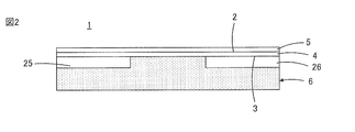
- FIG. 2 is a plan view showing a film 4 on which resistor films 7 to 12 provided for the pressing force sensor 1 according to the first embodiment of the present invention are formed. It is sectional drawing which shows the pressing force sensor 1 provided with the film 4 shown in FIG.
- FIG. 2 is a cross-sectional view showing a part of the pressing force sensor 1 in order to illustrate a pressing operation on the film 4 shown in FIG. 1. It is a figure which shows the circuit advantageously used for the pressing force detection by the pressing force sensor 1 shown in FIG.
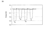
- FIG. 2 is a diagram showing output voltages obtained when pressing is performed on resistors R1 to R4 provided by pressing force detection resistor films 7 to 10 in the pressing force sensor 1 shown in FIG.
- FIG. 8 is a plan view showing a piezoelectric film 41 used in the pressing force sensor shown in FIG. 7 and a resin film 42 used overlapping therewith.
- the pressing force sensor 1 is disposed along a stretchable film 4 having a first main surface 2 and a second main surface 3 facing each other, and the first main surface 2 of the film 4.
- positioned along the 2nd main surface 3 of the film 4 are provided.
- the film 4, the protective film 5, and the support 6 are preferably joined to each other by an adhesive.
- the adhesiveness of the film 4 is bad or the heat resistance of the film 4 is low, it may be effective to use a thermoplastic adhesive as the adhesive.
- the film 4 is made of, for example, polyethylene terephthalate (PET), polyethylene naphthalate (PEN), polyimide, or the like.
- the protective film 5 is preferably made of a resin material having a Young's modulus lower than that of the film 4.
- the resistor films 7 to 12 are formed by printing carbon paste, for example.
- the six resistor films 7 to 12 provide resistances R1 to R6 for constituting the bridge circuit shown in FIG. 4, respectively, and at each end of the resistor films 7 to 12 are shown in FIG.
- Conductor lines 13 to 21 necessary for constituting the bridge circuit shown are connected.
- each of the conductor lines 7 to 12 is represented by one line, but actually, it has a predetermined width direction dimension.
- the conductor lines 7 to 12 are formed on the first main surface 2 of the film 4 by printing using, for example, silver paste.
- the resistor films 7 to 12 and the conductor lines 13 to 21 may be formed not on the first main surface 2 of the film 4 but on the second main surface 3 facing the support 6 side.
- the protective film 5 can be omitted.
- the four resistor films 7 to 10 serve as pressing force detection resistor films.
- the support 6 is provided with four recesses 23 to 26 as shown by broken lines in FIG.
- the recesses 23 to 26 have openings located in regions where the pressing force detection resistor films 7 to 10 are located, respectively.
- the recesses 23 to 26 may be replaced with holes that penetrate the support 6 in the thickness direction.
- the pressing force sensor 1 For the pressing force sensor 1 having the above-described configuration, as shown in FIG. 3, for example, when a pressing force in the direction indicated by the arrow 27 is applied toward the region where the opening of the recess 23 is located, The film 4 is deformed so as to fall into the recess 23, and accordingly, the film 4 extends in the recess 23. Due to the elongation of the film 4, the pressing force detecting resistor film 7 (see FIG. 1) at the position of the recess 23 is deformed due to distortion. As a result, the resistance value of the pressing force detecting resistor film 7 increases. On the other hand, if the pressing force is removed, the film 4 returns to the original flat state.
- the resistors R1 to R6 are respectively provided by the resistor films 7 to 12 included in the pressing force sensor 1, as described above.
- the other resistors R7 and R8 and operational amplifiers U1 and U2 are provided by an external circuit.
- the resistors R1, R2, R5 and R6 constitute a first bridge, and the resistors R3, R4, R5 and R6 constitute a second bridge.
- the voltages at the connection points 31, 32 and 33 are represented by voltages V1, V2 and V3, respectively.
- the output OUT1 becomes equal to the voltage between the resistors R5 and R6.
- the bridge is hardly in a completely balanced state. Even when the bridge is not pressed, a very small amount of current is applied to the resistors R7 and R8. Is flowing. Therefore, it is designed so that the voltage at the time when it is not pressed is recognized as software in the reference state (the state where it is not pressed).
- the resistor R3 works in the same way as the resistor R1
- the resistor R4 works in the same way as the resistor R2.
- resistors R5 and R6 provided by the resistor films 11 and 12 are not subjected to a pressing operation, and therefore do not need to be provided in the pressing force sensor 1 and may be provided by an external circuit.
- the resistors R5 and R6 are constituted by separate parts such as chip resistors, there is a possibility that the relative values of the respective resistance values (R1 / R2, R3 / R4, R5 / R6) may be shifted due to individual differences in resistance values. Get higher. Since the pressing force sensor 1 needs to detect a minute resistance change, an offset voltage is generated when the relative value of each resistance value described above varies, and the dynamic range of the detection sensitivity is lowered.
- the resistors R5 and R6 are also formed simultaneously with the resistor films 11 and 12 that are formed by printing simultaneously with the pressing force detecting resistor films 7 to 10 to be the resistors R1 to R4. If it is given by the above, the above problem of variation can be reduced.
- the meander-like resistor films 7 and 8 for providing the paired resistors R1 and R2 respectively face the same direction as shown in FIG.
- the body films 11 and 12 are also preferably oriented in the same direction. For example, in forming the resistor films 7 to 12, when the resistor paste is printed by applying screen printing, the resistance value may differ depending on the direction in which the squeegee runs. If the directions of the resistor films are aligned, the relative difference in the resistance value between the resistor films forming a pair can be reduced.
- the resistance values of the resistors R1 to R6 forming the bridge are in the range of 10 k ⁇ to 10 M ⁇ , and preferably about 100 k ⁇ to 1 ⁇ .
- the resistance value is low, a large amount of current flows, so that power consumption increases.
- the resistance value is high, it is easily affected by noise.
- FIG. 5 shows the detection of the pressing force that provides the resistance R1 in the portion where the recesses 23 to 26 of the support 6 are located in the pressing force sensor 1 designed so that the resistance values of the resistors R1 to R6 are about 700 k ⁇ .
- Resistor film 7 for pressing force detection resistor film 8 for providing resistance R2 pressing force detection resistor film 9 for providing resistance R3, and pressing force detection resistor film 10 for providing resistance R4
- the measurement result of the output voltage obtained when the pressing force of about 400 gf is sequentially applied is shown.
- the measurement result shown in FIG. 5 differs from the circuit shown in FIG. 4 in that the resistance change of each of the resistors R1 to R4 is detected independently.
- FIG. 6 is a diagram corresponding to FIG. 3 in the first embodiment.
- the pressing operation member 36 is attached to the film 4 side in order to transmit a pressing operation by an operator's finger 35 to the main surface of the film 4.
- the pressing operation member 36 has a shape including a shaft portion 37 and a flange portion 38, the shaft portion 37 functions as an action portion for the film 4, and the flange portion 38 provides a surface for receiving a pressing operation by the finger 35.
- An elastic body 39 is preferably disposed between the pressing operation member 36 and the film 4 in order to stabilize the posture of the pressing operation member 36.
- the film 4 When the pressing operation member 36 is pressed by the operator's finger 35 toward, for example, the region where the opening of the recess 23 is located in the film 4, the film 4 is deformed so as to fall into the recess 23. The film 4 stretches within 23. On the other hand, if the pressing force is removed, the film 4 returns to the original flat state.
- the heat of the finger 35 is hardly transmitted to the film 4. Therefore, it is possible to advantageously avoid the problem of false detection caused by the resistance value change due to the temperature change. Therefore, more accurate detection is possible.
- FIG. 7 is a diagram corresponding to FIG. 2 in the first embodiment.
- elements corresponding to the elements shown in FIG. 2 are denoted by the same reference numerals, and redundant description is omitted.
- the pressing force sensor 1 b shown in FIG. 7 further includes a piezoelectric film 41 and a resin film 42 arranged along the film 4.
- FIG. 8A shows an electrode pattern formed on the piezoelectric film 41
- FIG. 8B shows an electrode pattern formed on the resin film.
- the piezoelectric film 41 is made of a polymer having piezoelectricity such as polylactic acid or polyvinylidene fluoride.
- electrodes 43 to 46 are formed at positions corresponding to the positions of the pressing force detecting resistor films 7 to 8 formed on the film 4 described above.
- lead lines 47 to 50 drawn from the electrodes 43 to 46 are formed on one main surface of the piezoelectric film 41.
- Resin film 42 is made of, for example, an electrically insulating polymer such as polyethylene terephthalate.
- electrodes 51 to 54 are formed at positions facing the electrodes 43 to 46, respectively.
- the electrodes 51 to 54 are connected to each other by a connection line 55 and drawn out by a lead line 56. Note that the electrodes 51 to 54 may be replaced with electrodes in which these are integrated.
- the piezoelectric film 41 has two types of uses.
- the first use is as follows.
- a sensor using a resistor such as the pressing force sensor according to the present invention, consumes a current when detecting the pressing force, so that power consumption increases. Therefore, when not in use, power consumption can be reduced by setting the pressing force sensor to the sleep state and detecting the wake-up operation by the piezoelectric film 41. That is, when a pressing operation is performed on any of the pressing force detection resistor films 7 to 10, this pressing operation is transmitted to the piezoelectric film 41, and the piezoelectric film 41 is also deformed thereby. The deformation of the piezoelectric film 41 generates a charge due to the piezoelectric effect, and this charge is taken out by any of the electrodes 43 to 46 and any of the electrodes 51 to 54. Then, a signal obtained by the charge thus extracted may be used as a signal for starting the wake-up operation.
- polylactic acid As the material of the piezoelectric film 41 in that it produces piezoelectricity only by stretching and does not require poling treatment. Polylactic acid is also superior in that it is not pyroelectric and is not affected by temperature. Polylactic acid includes L-type polylactic acid (PLLA) and D-type polylactic acid (PDLA), but PLLA is preferably used because it is easily available.
- PLLA L-type polylactic acid
- PDLA D-type polylactic acid
- the second usage is as follows.
- polyvinylidene fluoride is used as the material of the piezoelectric film 41
- a temperature change can also be detected by the pyroelectric property of the polyvinylidene fluoride. Therefore, as in the case where the pressing operation member 36 used in the above-described second embodiment is not used, a process for canceling a change in resistance value due to a temperature change due to heat transfer from the finger is performed in software. It becomes possible to do.
- the resin film 42 is omitted. can do.
Landscapes
- Physics & Mathematics (AREA)
- General Physics & Mathematics (AREA)
- Force Measurement Appropriate To Specific Purposes (AREA)
- Measurement Of Force In General (AREA)
Description
この発明は、押圧力センサに関するもので、特に、抵抗体膜を用いて構成される押圧力センサに関するものである。
この発明にとって興味ある押圧力センサとして、たとえば特許第3855410号公報(特許文献1)に記載されたものがある。特許文献1には、たとえばカーボンペーストのような抵抗ペーストを絶縁基板上に印刷して抵抗体を形成し、この抵抗体に加えられる機械的な歪みを抵抗値変化として検出する歪ゲージが記載されている。
特許文献1に記載の歪ゲージでは、絶縁基板として、たとえば、表面を絶縁化したリン青銅板といった比較的剛性の高いものが用いられ、このような比較的剛性の高い絶縁基板上に抵抗体が形成されたユニモルフ構造が採用されている。また、抵抗体は、圧縮方向および引張方向のいずれかの応力を受ける。
しかしながら、特許文献1に記載の歪ゲージでは、以下のような課題がある。
ユニモルフ構造であるので、押圧力のほとんどは絶縁基板の変形エネルギーに費やされる。また、抵抗体は、圧縮および引張の両方の応力を受けるため、両方向の応力に対して対称的な抵抗変化が求められる。
そこで、この発明の目的は、上述した課題を解決し得る押圧力センサを提供しようとすることである。
この発明は、上述した技術的課題を解決するため、次のような構成を備えることを特徴としている。
この発明に係る押圧力センサは、伸縮可能なフィルムと、フィルムの主面の一部上に形成される押圧力検出用抵抗体膜と、フィルムの主面に沿って配置される支持体と、を備える。支持体には、フィルムの主面における押圧力検出用抵抗体膜が位置する領域に開口を位置させている凹部または孔が設けられる。
この押圧力センサでは、フィルムの主面に向かって押圧力を及ぼすと、フィルムが押圧力検出用抵抗体膜を伴って伸長する。その結果、押圧力検出用抵抗体膜が歪み、この歪みに応じた押圧力検出用抵抗体膜の抵抗値の変化が検出される。
この発明に係る押圧力センサは、好ましくは、第1ペアを組む第1抵抗および第2抵抗と第2ペアを組む第3抵抗および第4抵抗とからなるブリッジ回路において、第1抵抗および/または第2抵抗の抵抗値変化を検出することによって、押圧力を検出するようにされる。この好ましい実施態様において、上記第1抵抗および第2抵抗が、それぞれ、前述の押圧力検出用抵抗体膜によって与えられる。
上述の好ましい実施態様において、第3抵抗および第4抵抗が、それぞれ、フィルムの主面上に形成される、押圧力検出用抵抗体膜とは別の抵抗体膜によって与えられることがより好ましい。この実施態様によれば、第1ないし第4抵抗のすべてが、同じフィルムの主面上に形成される抵抗体膜によって与えられるので、第1ないし第4抵抗を同時に形成することができ、また、第1ないし第4抵抗の各々の抵抗値のばらつきを抑制することができる。
この発明に係る押圧力センサは、操作者の指による押圧操作をフィルムの主面に伝達するため、フィルム側に取り付けられる押圧操作部材をさらに備えていてもよい。押圧操作部材は、操作者の指の熱が押圧力検出用抵抗体膜に伝わりにくくするので、誤動作が生じる可能性を低くすることができる。
この発明に係る押圧力センサは、フィルムに沿って配置される圧電性フィルムをさらに備えていてもよい。この圧電性フィルムには、2種類の用途がある。第1に、この発明に係る押圧力センサのように、抵抗体を用いるセンサでは、押圧力検出の際、電流を消費するため、消費電力が大きくなる。そのため、不使用時には、センサをスリープ状態にしておき、ウェイクアップ動作を圧電性フィルムで検出するようにすれば、消費電力を小さくすることができる。第2に、圧電性フィルムの材料として、ポリフッ化ビニリデンを用いた場合、ポリフッ化ビニリデンが有する焦電性によって温度変化も検知することができる。したがって、温度変化による抵抗値の変化をキャンセルするような処理をソフトウェア的に行なうことが可能になる。
この発明に係る押圧力センサによれば、フィルムの主面に向かって押圧力を及ぼすと、押圧力が直接的にフィルムを伸長させ、このフィルムの伸長によって押圧力検出用抵抗体膜が効果的に歪みを受けて変形する。したがって、押圧力センサは、安価でありながら、高い感度を実現することができる。
また、フィルムは、引張方向にしか応力を受けないため、圧縮方向に対する感度と引張方向に対する感度とに差がある抵抗材料であっても、これを押圧力検出用抵抗体膜の材料として問題なく用いることができる。
[第1の実施形態]
図1ないし図5を参照して、第1の実施形態による押圧力センサ1について説明する。
図1ないし図5を参照して、第1の実施形態による押圧力センサ1について説明する。
押圧力センサ1は、図2に示すように、互いに対向する第1主面2および第2主面3を有する伸縮可能なフィルム4と、フィルム4の第1主面2に沿って配置される保護フィルム5と、フィルム4の第2主面3に沿って配置される支持体6と、を備えている。これらフィルム4、保護フィルム5および支持体6は、接着剤によって互いに接合されることが好ましい。なお、フィルム4の接着性が悪かったり、フィルム4の耐熱性が低かったりするときには、接着剤として、熱可塑性接着剤を用いることが有効な場合がある。
フィルム4は、たとえば、ポリエチレンテレフタレート(PET)、ポリエチレンナフタレート(PEN)、ポリイミドなどから構成される。保護フィルム5は、フィルム4よりもヤング率の低い樹脂材料から構成されることが好ましい。支持体6としては、たとえば、樹脂板、ステンレス鋼板またはプリント回路基板が用いられる。
フィルム4の第1主面2の一部上には、図1に示すように、各々ミアンダ状の6つの抵抗体膜7~12が形成されている。抵抗体膜7~12は、たとえば、カーボンペーストの印刷によって形成される。
6つの抵抗体膜7~12は、図4に示したブリッジ回路を構成するための抵抗R1~R6をそれぞれ与えるもので、抵抗体膜7~12の各々の各端部には、図4に示したブリッジ回路を構成するために必要な導体ライン13~21が接続されている。図1では、導体ライン7~12の各々を1本の線によって表現したが、実際には、所定の幅方向寸法を有している。導体ライン7~12は、フィルム4の第1主面2上にたとえば銀ペーストを用いた印刷により形成される。
図1に示した導体ラインと、図4に示した回路図に表示された導体ラインとの対応関係がわかるように、図4において、図1に示した導体ラインについての参照符号「13」~「21」が対応の導体ラインに付されている。
なお、抵抗体膜7~12および導体ライン13~21は、フィルム4の第1主面2上ではなく、支持体6側に向く第2主面3上に形成されてもよい。この場合には、保護フィルム5を省略することも可能である。
6つの抵抗体膜7~12のうち、4つの抵抗体膜7~10が押圧力検出用抵抗体膜となるものである。支持体6には、図1において破線で示すように、4つの凹部23~26が設けられている。凹部23~26は、それぞれ、押圧力検出用抵抗体膜7~10が位置する領域に開口を位置させている。なお、凹部23~26は、支持体6を厚み方向に貫通する孔に置き換えられてもよい。
以上のような構成を備える押圧力センサ1に対して、図3に示すように、フィルム4における、たとえば凹部23の開口が位置する領域に向かって矢印27で示す方向の押圧力を加えると、フィルム4は凹部23内に陥るように変形し、これに伴って、凹部23内でフィルム4が伸長する。このフィルム4の伸長によって、凹部23の位置にある押圧力検出用抵抗体膜7(図1参照)が歪みを受けて変形する。その結果、押圧力検出用抵抗体膜7の抵抗値が上昇する。他方、上記押圧力を除去すれば、フィルム4は、元の平坦な状態に戻る。
同様のことが、他の押圧力検出用抵抗体膜8~10についても言える。
なお、図3では、保護フィルム5の図示が省略されている。
次に、図4に示した押圧力検出回路の動作について説明する。この回路において、抵抗R1~R6は、前述したとおり、それぞれ、押圧力センサ1に備える抵抗体膜7~12によって与えられるものである。それ以外の抵抗R7およびR8、ならびにオペアンプU1およびU2は、外部回路によって与えられる。
図4に示したブリッジ回路において、抵抗R1、R2、R5およびR6によって第1のブリッジが構成され、抵抗R3、R4、R5およびR6によって第2のブリッジが構成される。図4において、接続点31、32および33での電圧が、それぞれ電圧V1、V2およびV3で表わされている。
押圧力センサ1における押圧力検出用抵抗体膜7~10のいずれに対しても、押圧力が及ぼされていないとき、特に、押圧力検出用抵抗体膜7および8のいずれにも、押圧力が及ぼされていないときには、第1のブリッジが平衡状態(R5/R6=R1/R2)となり、接続点31での電圧V1および接続点33での電圧V3については、V1=V3となる。このとき、抵抗R7には電流が流れず、出力OUT1は、抵抗R5と抵抗R6との間の電圧と等しくなる。
他方、押圧力検出用抵抗体膜9および10のいずれにも、押圧力が及ぼされていないときには、第2のブリッジが平衡状態(R5/R6=R3/R4)となり、接続点32での電圧V2および接続点33での電圧V3については、V2=V3となる。このとき、抵抗R8には電流が流れず、出力OUT2は、抵抗R5と抵抗R6との間の電圧と等しくなる。
ただし、実際には、抵抗R1~R6の各抵抗値にはばらつきがあるため、ブリッジが完全に平衡状態となることはほとんどなく、押圧されていない場合でも、微量の電流が抵抗R7および抵抗R8に流れている。したがって、押圧されていない時点での電圧が基準状態(押圧されていない状態)であるとソフトウェア的に認識するように設計される。
第1のブリッジにおいて、まず、押圧力検出用抵抗体膜7に押圧力が及ぼされると、これに対応する抵抗R1の抵抗値が上がる。これによって、接続点31での電圧V1が下がるが、第1のブリッジの平衡状態が崩れるため、オペアンプU1は、V1=V3を維持しようとする。すなわち、抵抗R7から抵抗R2に電流が流れるようにする。その結果、出力OUT1として、(V3+R7×電流値)が検出される。
他方、押圧力検出用抵抗体膜8に押圧力が及ぼされると、これに対応する抵抗R2の抵抗値が上がる。これによって、接続点31での電圧V1が上がるが、第1のブリッジの平衡状態が崩れるため、オペアンプU1は、V1=V3を維持しようとする。すなわち、抵抗R1から抵抗R2に流れていた電流の一部が抵抗R7に流れるようにする。その結果、出力OUT1として、(V3-R7×電流値)が検出される。
第2のブリッジについても同様である。この場合、抵抗R3は抵抗R1と同様に働き、抵抗R4は抵抗R2と同様に働く。
第2のブリッジにおいて、まず、押圧力検出用抵抗体膜9に押圧力が及ぼされると、これに対応する抵抗R3の抵抗値が上がる。これによって、接続点32での電圧V2が下がるが、第2のブリッジの平衡状態が崩れるため、オペアンプU2は、V2=V3を維持しようとする。すなわち、抵抗R8から抵抗R4に電流が流れるようにする。その結果、出力OUT2として、(V3+R8×電流値)が検出される。
他方、押圧力検出用抵抗体膜10に押圧力が及ぼされると、これに対応する抵抗R4の抵抗値が上がる。これによって、接続点32での電圧V2が上がるが、第2のブリッジの平衡状態が崩れるため、オペアンプU2は、V2=V3を維持しようとする。すなわち、抵抗R3から抵抗R4に流れていた電流の一部が抵抗R8に流れるようにする。その結果、出力OUT2として、(V3-R8×電流値)が検出される。
以上のようにして、押圧力センサ1における押圧力検出用抵抗体膜7~10のいずれが押圧されたか、また、その押圧力がどれほどであるかが検出される。
なお、抵抗体膜11および12によって与えられる抵抗R5およびR6については、押圧操作を受けるものではないので、押圧力センサ1内に設ける必要はなく、外部回路によって与えられてもよい。
しかしながら、抵抗R5およびR6をチップ抵抗などの別部品で構成すると、抵抗値の個体差により、各抵抗値の相対値(R1/R2、R3/R4、R5/R6)にずれが生じる可能性が高くなる。押圧力センサ1では、微小な抵抗変化を検出する必要があるので、上述した各抵抗値の相対値にばらつきがあると、オフセット電圧が発生し、検出感度のダイナミックレンジを下げてしまう。これに対して、この実施形態のように、抵抗R5およびR6についても、抵抗R1~R4となるべき押圧力検出用抵抗体膜7~10と同時に印刷して形成される抵抗体膜11および12によって与えるようにすれば、上記のばらつきの問題を低減することができる。
ブリッジ回路において、ペアを組む抵抗R1およびR2をそれぞれ与えるミアンダ状の抵抗体膜7および8は、図1に示すように、互いに同じ方向を向いていることが好ましい。同様に、ペアを組む抵抗R3およびR4をそれぞれ与えるミアンダ状の抵抗体膜9および10についても、互いに同じ方向を向いていることが好ましく、ペアを組む抵抗R5およびR6をそれぞれ与えるミアンダ状の抵抗体膜11および12についても、互いに同じ方向を向いていることが好ましい。たとえば、抵抗体膜7~12を形成するにあたって、スクリーン印刷を適用して抵抗体ペーストを印刷するとき、スキージの走る方向によって抵抗値が異なることがあり得るが、上記のように、ペアを組む抵抗体膜同士の向きを揃えておけば、ペアを組む抵抗体膜間の抵抗値の相対的差異を小さくすることができる。
ブリッジを組む抵抗R1~R6の各々の抵抗値は、10kΩ~10MΩの範囲にあり、好ましくは、100kΩ~1Ω程度である。抵抗値が低いと多くの電流が流れるため、消費電力が大きくなる。他方、抵抗値が高いとノイズの影響を受けやすくなる。
図5には、抵抗R1~R6の各々の抵抗値が約700kΩとなるように設計した押圧力センサ1について、支持体6の凹部23~26が位置する部分において、抵抗R1を与える押圧力検出用抵抗体膜7、抵抗R2を与える押圧力検出用抵抗体膜8、抵抗R3を与える押圧力検出用抵抗体膜9、および抵抗R4を与える押圧力検出用抵抗体膜10の各々に向かって約400gfの押圧力を順次加えた場合に得られた出力電圧の測定結果が示されている。図5に示した測定結果は、図4に示すような回路とは異なり、抵抗R1~R4の各々の抵抗変化を独立して検出したものである。
[第2の実施形態]
図6を参照して、第2の実施形態による押圧力センサ1aについて説明する。図6は、第1の実施形態における図3に対応する図である。図6において、図3に示した要素に相当する要素には同様の参照符号を付し、重複する説明は省略する。
図6を参照して、第2の実施形態による押圧力センサ1aについて説明する。図6は、第1の実施形態における図3に対応する図である。図6において、図3に示した要素に相当する要素には同様の参照符号を付し、重複する説明は省略する。
図6に示した押圧力センサ1aは、操作者の指35による押圧操作をフィルム4の主面に伝達するため、フィルム4側に押圧操作部材36が取り付けられていることを特徴としている。押圧操作部材36は、軸部37とフランジ部38とからなる形状を有し、軸部37がフィルム4に対する作用部として機能し、フランジ部38が指35による押圧操作を受ける面を与える。押圧操作部材36とフィルム4との間には、押圧操作部材36の姿勢を安定させるため、弾性体39が配置されることが好ましい。
操作者の指35によって、フィルム4における、たとえば凹部23の開口が位置する領域に向かって押圧操作部材36を押圧すると、フィルム4は凹部23内に陥るように変形し、これに伴って、凹部23内でフィルム4が伸長する。他方、上記押圧力を除去すれば、フィルム4は、元の平坦な状態に戻る。
この実施形態によれば、指35の熱がフィルム4に伝わりにくくなる。したがって、温度変化による抵抗値変化がもたらす誤検知の問題を有利に回避することができる。よって、より正確な検知が可能になる。
[第3の実施形態]
図7および図8を参照して、第3の実施形態による押圧力センサ1bについて説明する。図7は、第1の実施形態における図2に対応する図である。図7において、図2に示した要素に相当する要素には同様の参照符号を付し、重複する説明は省略する。
図7および図8を参照して、第3の実施形態による押圧力センサ1bについて説明する。図7は、第1の実施形態における図2に対応する図である。図7において、図2に示した要素に相当する要素には同様の参照符号を付し、重複する説明は省略する。
図7を図2と対比すればわかるように、図7に示した押圧力センサ1bは、フィルム4に沿って配置される圧電性フィルム41および樹脂フィルム42をさらに備えることを特徴としている。図8(A)には、圧電性フィルム41上に形成される電極パターンが示され、図8(B)には、樹脂フィルム42上に形成される電極パターンが示されている。
圧電性フィルム41は、たとえば、ポリ乳酸、ポリフッ化ビニリデンのような圧電性を有するポリマーから構成される。圧電性フィルム41の一方主面上には、前述したフィルム4上に形成された押圧力検出用抵抗体膜7~8の各位置に対応する位置に、電極43~46が形成される。また、電極43~46の各々から引き出される引出しライン47~50が、圧電性フィルム41の一方主面上に形成される。
樹脂フィルム42は、たとえば、ポリエチレンテレフタレートのような電気絶縁性のポリマーから構成される。樹脂フィルム42の一方主面上には、上述した電極43~46にそれぞれ対向する位置に電極51~54が形成される。樹脂フィルム42の一方主面上において、電極51~54は、接続ライン55によって互いに接続され、また、引出しライン56によって引き出される。なお、電極51~54は、これらを一体化した電極に置き換えられてもよい。
この実施形態において、圧電性フィルム41には、2種類の用途がある。
第1の用途は以下のとおりである。この発明に係る押圧力センサのように、抵抗体を用いるセンサでは、押圧力検出の際、電流を消費するため、消費電力が大きくなる。そのため、不使用時には、押圧力センサをスリープ状態にしておき、ウェイクアップ動作を圧電性フィルム41で検出するようにすれば、消費電力を小さくすることができる。すなわち、押圧力検出用抵抗体膜7~10のいずれかに対して押圧操作を実施したとき、この押圧操作が圧電性フィルム41にも伝わり、それによって圧電性フィルム41も変形する。この圧電性フィルム41の変形は圧電効果による電荷を発生させ、この電荷が電極43~46のいずれかと電極51~54のいずれかとによって取り出される。そして、このように取り出した電荷によって得られた信号を、ウェイクアップ動作を起動するための信号として用いればよい。
第1の用途の場合には、圧電性フィルム41の材料として、延伸のみで圧電性を生じ、ポーリング処理を施す必要がない点で、ポリ乳酸を用いることが好ましい。また、ポリ乳酸は、焦電性がなく、よって、温度の影響を受けない点でも優れている。ポリ乳酸には、L型ポリ乳酸(PLLA)とD型ポリ乳酸(PDLA)とが存在するが、入手容易な点で、PLLAを用いることが好ましい。
第2の用途は以下のとおりである。圧電性フィルム41の材料として、ポリフッ化ビニリデンを用いた場合、ポリフッ化ビニリデンが有する焦電性によって温度変化も検知することができる。したがって、前述の第2の実施形態において用いた押圧操作部材36を用いない場合のように、指からの熱の伝達による温度変化に起因する抵抗値の変化をキャンセルするような処理をソフトウェア的に行なうことが可能になる。
なお、第3の実施形態において、圧電性フィルム41の一方主面上に電極43~46を形成しながら、他方主面上に電極51~54を形成するようにすれば、樹脂フィルム42は省略することができる。
1,1a,1b 押圧力センサ
2,3 主面
4 フィルム
6 支持体
7~10 押圧力検出用抵抗体膜
11,12 抵抗体膜
13 導体ライン
23~26 凹部
36 押圧操作部材
41 圧電性フィルム
2,3 主面
4 フィルム
6 支持体
7~10 押圧力検出用抵抗体膜
11,12 抵抗体膜
13 導体ライン
23~26 凹部
36 押圧操作部材
41 圧電性フィルム
Claims (5)
- 伸縮可能なフィルムと、
前記フィルムの主面の一部上に形成される押圧力検出用抵抗体膜と、
前記フィルムの主面に沿って配置される支持体と、
を備え、
前記支持体には、前記フィルムの前記押圧力検出用抵抗体膜が位置する領域に開口を位置させている凹部または孔が設けられ、
前記フィルムの主面に向かって及ぼされた押圧力が前記押圧力検出用抵抗体膜を歪ませることによって生じる前記押圧力検出用抵抗体膜の抵抗値の変化を検出するようにした、
押圧力センサ。 - 第1ペアを組む第1抵抗および第2抵抗と第2ペアを組む第3抵抗および第4抵抗とからなるブリッジ回路において、前記第1抵抗および/または前記第2抵抗の抵抗値変化を検出することによって、押圧力を検出するようにした、押圧力センサであって、
前記第1抵抗および前記第2抵抗が、それぞれ、前記押圧力検出用抵抗体膜によって与えられる、
請求項1に記載の押圧力センサ。 - 前記第3抵抗および前記第4抵抗が、それぞれ、前記フィルムの主面上に形成される抵抗体膜によって与えられる、請求項2に記載の押圧力センサ。
- 操作者の指による押圧操作を前記フィルムの主面に伝達するため、前記フィルム側に取り付けられる押圧操作部材をさらに備える、請求項1ないし3のいずれかに記載の押圧力センサ。
- 前記フィルムに沿って配置される圧電性フィルムをさらに備える、請求項1ないし4のいずれかに記載の押圧力センサ。
Priority Applications (2)
| Application Number | Priority Date | Filing Date | Title |
|---|---|---|---|
| JP2014526801A JP5854143B2 (ja) | 2012-07-26 | 2013-06-01 | 押圧力センサ |
| US14/603,483 US9528890B2 (en) | 2012-07-26 | 2015-01-23 | Pressing force sensor |
Applications Claiming Priority (2)
| Application Number | Priority Date | Filing Date | Title |
|---|---|---|---|
| JP2012165736 | 2012-07-26 | ||
| JP2012-165736 | 2012-07-26 |
Related Child Applications (1)
| Application Number | Title | Priority Date | Filing Date |
|---|---|---|---|
| US14/603,483 Continuation US9528890B2 (en) | 2012-07-26 | 2015-01-23 | Pressing force sensor |
Publications (1)
| Publication Number | Publication Date |
|---|---|
| WO2014017169A1 true WO2014017169A1 (ja) | 2014-01-30 |
Family
ID=49996987
Family Applications (1)
| Application Number | Title | Priority Date | Filing Date |
|---|---|---|---|
| PCT/JP2013/065297 Ceased WO2014017169A1 (ja) | 2012-07-26 | 2013-06-01 | 押圧力センサ |
Country Status (3)
| Country | Link |
|---|---|
| US (1) | US9528890B2 (ja) |
| JP (1) | JP5854143B2 (ja) |
| WO (1) | WO2014017169A1 (ja) |
Cited By (1)
| Publication number | Priority date | Publication date | Assignee | Title |
|---|---|---|---|---|
| JP2020118534A (ja) * | 2019-01-23 | 2020-08-06 | マツダ株式会社 | 金型の成形時荷重計測装置及びその方法 |
Families Citing this family (7)
| Publication number | Priority date | Publication date | Assignee | Title |
|---|---|---|---|---|
| EP2696163B1 (en) | 2011-04-08 | 2018-05-23 | Murata Manufacturing Co., Ltd. | Displacement sensor, displacement detecting apparatus, and operation device |
| WO2014017407A1 (ja) * | 2012-07-26 | 2014-01-30 | 株式会社村田製作所 | 押圧力センサ |
| CN106325579B (zh) * | 2015-07-10 | 2023-04-07 | 宸鸿科技(厦门)有限公司 | 一种压力感测输入装置 |
| EP3430643B1 (en) * | 2016-03-15 | 2021-06-16 | AT & S Austria Technologie & Systemtechnik Aktiengesellschaft | Component carrier with integrated strain gauge |
| CN105975137B (zh) | 2016-07-07 | 2020-11-03 | 上海天马微电子有限公司 | 一种触控显示面板及触控显示装置 |
| CN106708327B (zh) * | 2017-01-21 | 2023-04-11 | 宸鸿科技(厦门)有限公司 | 压力传感器及显示装置 |
| CN118687458A (zh) * | 2023-03-23 | 2024-09-24 | 霍尼韦尔国际公司 | 用于检测表面上变形的方法、系统和设备 |
Citations (5)
| Publication number | Priority date | Publication date | Assignee | Title |
|---|---|---|---|---|
| JPS6358121A (ja) * | 1986-08-28 | 1988-03-12 | Meidensha Electric Mfg Co Ltd | 多機能マトリツクスセンサ |
| JPS63155676A (ja) * | 1986-12-19 | 1988-06-28 | Agency Of Ind Science & Technol | 触覚センサ |
| JP2002365151A (ja) * | 2001-06-12 | 2002-12-18 | Alps Electric Co Ltd | 荷重検出装置 |
| JP2004053424A (ja) * | 2002-07-19 | 2004-02-19 | Matsushita Electric Works Ltd | 機械的変形量検出センサ及びそれを用いた加速度センサ、圧力センサ |
| JP2010002407A (ja) * | 2008-06-20 | 2010-01-07 | Korea Research Inst Of Standards & Science | メンブレン構造を有する触覚センサー及びその製作方法 |
Family Cites Families (10)
| Publication number | Priority date | Publication date | Assignee | Title |
|---|---|---|---|---|
| US4188258A (en) * | 1978-05-18 | 1980-02-12 | Gulton Industries, Inc. | Process for fabricating strain gage transducer |
| DE3772514D1 (de) * | 1986-10-28 | 1991-10-02 | Sumitomo Electric Industries | Messverfahren fuer einen halbleiter-druckmessfuehler. |
| US4996627A (en) * | 1989-01-30 | 1991-02-26 | Dresser Industries, Inc. | High sensitivity miniature pressure transducer |
| JP3855410B2 (ja) | 1997-12-02 | 2006-12-13 | 松下電器産業株式会社 | 抵抗ペースト、これを用いた歪ゲージ及び多方向操作体 |
| DE102008011942A1 (de) * | 2008-02-29 | 2009-09-03 | Robert Bosch Gmbh | Schaltungsanordnung |
| US8174372B2 (en) * | 2008-06-26 | 2012-05-08 | Immersion Corporation | Providing haptic feedback on a touch surface |
| ATE523836T1 (de) * | 2008-07-07 | 2011-09-15 | Tyco Electronics Services Gmbh | Vorrichtung zur änderung des betriebszustandes eines geräts |
| JP2010152671A (ja) * | 2008-12-25 | 2010-07-08 | Sharp Corp | 表示装置 |
| JP5708214B2 (ja) * | 2011-03-28 | 2015-04-30 | セイコーエプソン株式会社 | 圧力センサー、センサーアレイ、センサーアレイの製造方法、及び把持装置 |
| US20130152694A1 (en) * | 2011-11-01 | 2013-06-20 | Ilkka Urvas | Sensor with vacuum cavity and method of fabrication |
-
2013
- 2013-06-01 JP JP2014526801A patent/JP5854143B2/ja active Active
- 2013-06-01 WO PCT/JP2013/065297 patent/WO2014017169A1/ja not_active Ceased
-
2015
- 2015-01-23 US US14/603,483 patent/US9528890B2/en active Active
Patent Citations (5)
| Publication number | Priority date | Publication date | Assignee | Title |
|---|---|---|---|---|
| JPS6358121A (ja) * | 1986-08-28 | 1988-03-12 | Meidensha Electric Mfg Co Ltd | 多機能マトリツクスセンサ |
| JPS63155676A (ja) * | 1986-12-19 | 1988-06-28 | Agency Of Ind Science & Technol | 触覚センサ |
| JP2002365151A (ja) * | 2001-06-12 | 2002-12-18 | Alps Electric Co Ltd | 荷重検出装置 |
| JP2004053424A (ja) * | 2002-07-19 | 2004-02-19 | Matsushita Electric Works Ltd | 機械的変形量検出センサ及びそれを用いた加速度センサ、圧力センサ |
| JP2010002407A (ja) * | 2008-06-20 | 2010-01-07 | Korea Research Inst Of Standards & Science | メンブレン構造を有する触覚センサー及びその製作方法 |
Cited By (2)
| Publication number | Priority date | Publication date | Assignee | Title |
|---|---|---|---|---|
| JP2020118534A (ja) * | 2019-01-23 | 2020-08-06 | マツダ株式会社 | 金型の成形時荷重計測装置及びその方法 |
| JP7139970B2 (ja) | 2019-01-23 | 2022-09-21 | マツダ株式会社 | 金型の成形時荷重計測装置及びその方法 |
Also Published As
| Publication number | Publication date |
|---|---|
| JP5854143B2 (ja) | 2016-02-09 |
| JPWO2014017169A1 (ja) | 2016-07-07 |
| US9528890B2 (en) | 2016-12-27 |
| US20150135857A1 (en) | 2015-05-21 |
Similar Documents
| Publication | Publication Date | Title |
|---|---|---|
| JP5854143B2 (ja) | 押圧力センサ | |
| JP6269899B2 (ja) | 圧電フィルムセンサおよび保持状態検出装置 | |
| US10842397B2 (en) | Flexible sensor and application thereof | |
| US6829942B2 (en) | Pressure sensor | |
| CN105793686B (zh) | 输入装置以及输入装置的控制方法 | |
| JP6624343B2 (ja) | センサ、タッチパネル、及び電子機器 | |
| JP6406473B2 (ja) | 押圧検出装置、電子機器 | |
| US20150233777A1 (en) | Strain transmitter | |
| CN204214475U (zh) | 一种假肢手穿戴式柔性触觉传感器及其触觉检测装置 | |
| US20080229841A1 (en) | Strain Sensor | |
| JP6285259B2 (ja) | 圧力センサ | |
| JP2006226858A (ja) | 変動荷重センサ及びこれを用いた触覚センサ | |
| JP6123614B2 (ja) | 押圧検出センサ、タッチ式入力装置 | |
| KR102256241B1 (ko) | 전단 및 수직 응력 감지 센서 및 이의 제조 방법 | |
| JP6973654B2 (ja) | タッチパネル | |
| CN107688405B (zh) | 触摸压力感测装置及电子产品 | |
| JPH0663725B2 (ja) | 圧電センサ | |
| JP2017198573A (ja) | 圧力検出装置 | |
| US20230008926A1 (en) | Sensor | |
| JP4488338B2 (ja) | 圧力検出装置 | |
| WO2022264641A1 (ja) | センサおよびセンサ処理装置 | |
| CN113296634B (zh) | 一种电子设备 | |
| CN113137910A (zh) | 复合式薄膜传感器 | |
| LU102398B1 (en) | Sensor device | |
| WO2025234304A1 (ja) | センサ |
Legal Events
| Date | Code | Title | Description |
|---|---|---|---|
| 121 | Ep: the epo has been informed by wipo that ep was designated in this application |
Ref document number: 13823222 Country of ref document: EP Kind code of ref document: A1 |
|
| ENP | Entry into the national phase |
Ref document number: 2014526801 Country of ref document: JP Kind code of ref document: A |
|
| NENP | Non-entry into the national phase |
Ref country code: DE |
|
| 122 | Ep: pct application non-entry in european phase |
Ref document number: 13823222 Country of ref document: EP Kind code of ref document: A1 |