WO2014016931A1 - 太陽電池及びその製造方法 - Google Patents
太陽電池及びその製造方法 Download PDFInfo
- Publication number
- WO2014016931A1 WO2014016931A1 PCT/JP2012/068922 JP2012068922W WO2014016931A1 WO 2014016931 A1 WO2014016931 A1 WO 2014016931A1 JP 2012068922 W JP2012068922 W JP 2012068922W WO 2014016931 A1 WO2014016931 A1 WO 2014016931A1
- Authority
- WO
- WIPO (PCT)
- Prior art keywords
- semiconductor layer
- type
- microcrystalline
- amorphous
- conductivity type
- Prior art date
- Legal status (The legal status is an assumption and is not a legal conclusion. Google has not performed a legal analysis and makes no representation as to the accuracy of the status listed.)
- Ceased
Links
Images

Classifications
-
- H—ELECTRICITY
- H10—SEMICONDUCTOR DEVICES; ELECTRIC SOLID-STATE DEVICES NOT OTHERWISE PROVIDED FOR
- H10F—INORGANIC SEMICONDUCTOR DEVICES SENSITIVE TO INFRARED RADIATION, LIGHT, ELECTROMAGNETIC RADIATION OF SHORTER WAVELENGTH OR CORPUSCULAR RADIATION
- H10F77/00—Constructional details of devices covered by this subclass
- H10F77/10—Semiconductor bodies
- H10F77/14—Shape of semiconductor bodies; Shapes, relative sizes or dispositions of semiconductor regions within semiconductor bodies
- H10F77/148—Shapes of potential barriers
-
- H—ELECTRICITY
- H10—SEMICONDUCTOR DEVICES; ELECTRIC SOLID-STATE DEVICES NOT OTHERWISE PROVIDED FOR
- H10F—INORGANIC SEMICONDUCTOR DEVICES SENSITIVE TO INFRARED RADIATION, LIGHT, ELECTROMAGNETIC RADIATION OF SHORTER WAVELENGTH OR CORPUSCULAR RADIATION
- H10F10/00—Individual photovoltaic cells, e.g. solar cells
- H10F10/10—Individual photovoltaic cells, e.g. solar cells having potential barriers
- H10F10/14—Photovoltaic cells having only PN homojunction potential barriers
- H10F10/146—Back-junction photovoltaic cells, e.g. having interdigitated base-emitter regions on the back side
-
- H—ELECTRICITY
- H10—SEMICONDUCTOR DEVICES; ELECTRIC SOLID-STATE DEVICES NOT OTHERWISE PROVIDED FOR
- H10F—INORGANIC SEMICONDUCTOR DEVICES SENSITIVE TO INFRARED RADIATION, LIGHT, ELECTROMAGNETIC RADIATION OF SHORTER WAVELENGTH OR CORPUSCULAR RADIATION
- H10F10/00—Individual photovoltaic cells, e.g. solar cells
- H10F10/10—Individual photovoltaic cells, e.g. solar cells having potential barriers
- H10F10/16—Photovoltaic cells having only PN heterojunction potential barriers
- H10F10/167—Photovoltaic cells having only PN heterojunction potential barriers comprising Group I-III-VI materials, e.g. CdS/CuInSe2 [CIS] heterojunction photovoltaic cells
-
- H—ELECTRICITY
- H10—SEMICONDUCTOR DEVICES; ELECTRIC SOLID-STATE DEVICES NOT OTHERWISE PROVIDED FOR
- H10F—INORGANIC SEMICONDUCTOR DEVICES SENSITIVE TO INFRARED RADIATION, LIGHT, ELECTROMAGNETIC RADIATION OF SHORTER WAVELENGTH OR CORPUSCULAR RADIATION
- H10F71/00—Manufacture or treatment of devices covered by this subclass
- H10F71/121—The active layers comprising only Group IV materials
-
- Y—GENERAL TAGGING OF NEW TECHNOLOGICAL DEVELOPMENTS; GENERAL TAGGING OF CROSS-SECTIONAL TECHNOLOGIES SPANNING OVER SEVERAL SECTIONS OF THE IPC; TECHNICAL SUBJECTS COVERED BY FORMER USPC CROSS-REFERENCE ART COLLECTIONS [XRACs] AND DIGESTS
- Y02—TECHNOLOGIES OR APPLICATIONS FOR MITIGATION OR ADAPTATION AGAINST CLIMATE CHANGE
- Y02E—REDUCTION OF GREENHOUSE GAS [GHG] EMISSIONS, RELATED TO ENERGY GENERATION, TRANSMISSION OR DISTRIBUTION
- Y02E10/00—Energy generation through renewable energy sources
- Y02E10/50—Photovoltaic [PV] energy
- Y02E10/541—CuInSe2 material PV cells
-
- Y—GENERAL TAGGING OF NEW TECHNOLOGICAL DEVELOPMENTS; GENERAL TAGGING OF CROSS-SECTIONAL TECHNOLOGIES SPANNING OVER SEVERAL SECTIONS OF THE IPC; TECHNICAL SUBJECTS COVERED BY FORMER USPC CROSS-REFERENCE ART COLLECTIONS [XRACs] AND DIGESTS
- Y02—TECHNOLOGIES OR APPLICATIONS FOR MITIGATION OR ADAPTATION AGAINST CLIMATE CHANGE
- Y02E—REDUCTION OF GREENHOUSE GAS [GHG] EMISSIONS, RELATED TO ENERGY GENERATION, TRANSMISSION OR DISTRIBUTION
- Y02E10/00—Energy generation through renewable energy sources
- Y02E10/50—Photovoltaic [PV] energy
- Y02E10/547—Monocrystalline silicon PV cells
-
- Y—GENERAL TAGGING OF NEW TECHNOLOGICAL DEVELOPMENTS; GENERAL TAGGING OF CROSS-SECTIONAL TECHNOLOGIES SPANNING OVER SEVERAL SECTIONS OF THE IPC; TECHNICAL SUBJECTS COVERED BY FORMER USPC CROSS-REFERENCE ART COLLECTIONS [XRACs] AND DIGESTS
- Y02—TECHNOLOGIES OR APPLICATIONS FOR MITIGATION OR ADAPTATION AGAINST CLIMATE CHANGE
- Y02P—CLIMATE CHANGE MITIGATION TECHNOLOGIES IN THE PRODUCTION OR PROCESSING OF GOODS
- Y02P70/00—Climate change mitigation technologies in the production process for final industrial or consumer products
- Y02P70/50—Manufacturing or production processes characterised by the final manufactured product
Definitions
- the present invention relates to a solar cell and a manufacturing method thereof.
- Patent Document 1 describes a back junction solar cell in which both a p-side electrode and an n-side electrode are provided on the back side as a solar cell that can improve photoelectric conversion efficiency.
- the solar cell described in Patent Document 1 is provided on a first semiconductor layer provided on a first region of one principal surface of a substrate made of a semiconductor material and on a second region on one principal surface. And a second semiconductor layer.
- One of the first and second semiconductor layers is p-type and the other is n-type.
- the second semiconductor layer is provided over the first semiconductor layer from the second region. In the first region, a recombination layer is provided between the first semiconductor layer and the second semiconductor layer.
- This recombination layer is a layer for reducing the resistance between the p-side electrode and the p-type amorphous semiconductor layer 11p.
- a substantially intrinsic i-type semiconductor layer is disposed between the second semiconductor layer and the recombination layer.
- the main object of the present invention is to provide a solar cell having improved photoelectric conversion efficiency.
- a solar cell according to the present invention includes a substrate made of a semiconductor material, a substantially intrinsic i-type semiconductor layer, a first amorphous semiconductor layer, a first microcrystalline semiconductor layer, and a second microcrystalline semiconductor layer. And a second amorphous semiconductor layer.
- the i-type semiconductor layer is disposed on one main surface of the substrate.
- the first amorphous semiconductor layer is disposed on a part of the i-type semiconductor layer.
- the first amorphous semiconductor layer has one conductivity type.
- the first microcrystalline semiconductor layer is disposed on the first amorphous semiconductor layer.
- the first microcrystalline semiconductor layer has one conductivity type.
- the second microcrystalline semiconductor layer is disposed on the first microcrystalline semiconductor layer.
- the second microcrystalline semiconductor layer has another conductivity type.
- the second amorphous semiconductor layer is arranged over the second microcrystalline semiconductor layer and the exposed portion of the i-type semiconductor layer from the second microcrystalline semiconductor layer.
- the second amorphous semiconductor layer has another conductivity type.
- the second amorphous semiconductor layer and the second microcrystalline semiconductor layer are in contact with each other.
- a substantially intrinsic i-type semiconductor layer is formed on one main surface of a substrate made of a semiconductor material.
- a first amorphous semiconductor layer having one conductivity type, a first microcrystalline semiconductor layer having one conductivity type, and a second microcrystalline semiconductor layer having another conductivity type are formed in this order.
- a part of the first amorphous semiconductor layer and the first and second microcrystalline semiconductor layers are removed by etching to partially expose the i-type semiconductor layer.
- a second amorphous semiconductor layer having another conductivity type is formed so as to straddle over the second microcrystalline semiconductor layer and the exposed portion of the i-type semiconductor layer.
- a solar cell having improved photoelectric conversion efficiency can be provided.
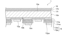
- FIG. 1 is a schematic cross-sectional view of a solar cell according to an embodiment of the present invention.
- FIG. 2 is a schematic cross-sectional view for explaining a manufacturing process of the solar cell in one embodiment of the present invention.
- the solar cell 1 has a substrate 10n made of a semiconductor material.
- the substrate 10n has n-type or p-type conductivity.
- the conductivity type of the substrate 10n is n-type.
- the substrate 10n can be made of, for example, an n-type crystalline semiconductor material.
- the substrate 10n can be composed of, for example, n-type crystalline silicon.
- the crystalline semiconductor material includes a single crystal semiconductor material and a polycrystalline semiconductor material. Crystalline silicon includes single crystal silicon and polycrystalline silicon.
- the substrate 10n has a first main surface 10a and a second main surface 10b that mainly receive light.
- the first main surface 10a is located on the light receiving surface side.
- the “light receiving surface” means a main surface on the side of mainly receiving light, out of the two main surfaces.
- a semiconductor layer 17i, a semiconductor layer 17n, and a protective layer 18 are provided in this order on the first main surface 10a.
- the semiconductor layer 17i is made of a substantially intrinsic i-type semiconductor material.
- the semiconductor layer 17i can be made of, for example, i-type amorphous silicon.
- the thickness of the semiconductor layer 17i is preferably a thickness that does not substantially contribute to power generation (for example, about 0.1 nm to 25 nm).
- the conductivity type of the semiconductor layer 17n is an n-type which is the same conductivity type as the substrate 10n.
- the semiconductor layer 17n can be made of, for example, n-type amorphous silicon.
- the protective layer 18 can be made of, for example, silicon nitride.
- the protective layer 18 may have a function of suppressing surface reflection of incident light as well as a function of protecting the semiconductor layer 17n.
- a substantially intrinsic i-type semiconductor layer 11ia is disposed on the second main surface 10b of the substrate 10n.
- the i-type semiconductor layer 11ia is disposed on substantially the entire second main surface 10b.
- the i-type amorphous semiconductor layer 11ia has a thickness that does not substantially contribute to power generation (for example, about 0.1 nm to 25 nm).
- the i-type amorphous semiconductor layer 11ia can be made of, for example, i-type amorphous silicon.
- the first amorphous semiconductor layer 11na is disposed on a part of the i-type semiconductor layer 11ia. For this reason, a part of the i-type semiconductor layer 11ia is exposed from the first amorphous semiconductor layer 11na.
- the first amorphous semiconductor layer 11na has the same conductivity type as the substrate 10n. Specifically, the conductivity type of the first amorphous semiconductor layer 11na is n-type. However, the first amorphous semiconductor layer 11na may have a conductivity type different from that of the substrate 10n.
- the first amorphous semiconductor layer 11na can be made of, for example, n-type amorphous silicon.
- the thickness of the first amorphous semiconductor layer 11na can be set to, for example, about 1 nm to 30 nm.
- the microcrystalline semiconductor layer 13 is disposed on the first amorphous semiconductor layer 11na.
- the thickness of the microcrystalline semiconductor layer 13 is preferably about 2 nm to 60 nm, for example, and more preferably 2 nm to 30 nm.
- the microcrystalline semiconductor layer 13 includes a first microcrystalline semiconductor layer 13nc and a second microcrystalline semiconductor layer 13pc.
- the first microcrystalline semiconductor layer 13nc is provided on the first amorphous semiconductor layer 11na.
- the first microcrystalline semiconductor layer 13nc is in contact with the first amorphous semiconductor layer 11na.
- the first microcrystalline semiconductor layer 13nc has the same conductivity type as the first amorphous semiconductor layer 11na.
- the conductivity type of the first microcrystalline semiconductor layer 13nc is n-type.
- the first microcrystalline semiconductor layer 13nc can be made of, for example, n-type microcrystalline silicon.
- the thickness of the first microcrystalline semiconductor layer 13nc is, for example, preferably about 1 nm to 30 nm, and more preferably 1 nm to 15 nm.
- the second microcrystalline semiconductor layer 13pc is disposed on the first microcrystalline semiconductor layer 13nc.
- the second microcrystalline semiconductor layer 13pc is in contact with each of the first microcrystalline semiconductor layer 13nc and a second amorphous semiconductor layer 12pa described later.
- Second microcrystalline semiconductor layer 13pc has a conductivity type different from that of first microcrystalline semiconductor layer 13nc. Specifically, the conductivity type of the second microcrystalline semiconductor layer 13pc is p-type.
- the second microcrystalline semiconductor layer 13pc can be made of, for example, p-type microcrystalline silicon.
- the thickness of the second microcrystalline semiconductor layer 13pc is, for example, preferably about 1 nm to 30 nm, and more preferably 1 nm to 15 nm.
- the microcrystalline semiconductor layer refers to a layer including a plurality of semiconductor crystal grains.
- the microcrystalline semiconductor layer includes a layer that substantially includes only semiconductor crystal grains.
- the microcrystalline semiconductor layer may include an amorphous region of a semiconductor in addition to the semiconductor crystal grains. Therefore, the microcrystalline semiconductor layer is a layer including a plurality of semiconductor crystal grains, and may be a layer including an amorphous region of a semiconductor similarly to the amorphous semiconductor layer.
- the second amorphous semiconductor layer 12pa is disposed on the second microcrystalline semiconductor layer 13pc and the exposed portion of the i-type semiconductor layer 11ia from the second microcrystalline semiconductor layer 13pc.
- the second amorphous semiconductor layer 12pa is arranged over the second microcrystalline semiconductor layer 13pc and the exposed portion of the i-type semiconductor layer 11ia from the second microcrystalline semiconductor layer 13pc. Yes.
- An i-type semiconductor layer is not provided between the second amorphous semiconductor layer 12pa and the second microcrystalline semiconductor layer 13pc.
- the second amorphous semiconductor layer 12pa is in direct contact with the second microcrystalline semiconductor layer 13pc.
- the second amorphous semiconductor layer 12pa has a conductivity type different from that of the substrate 10n.
- the conductivity type of the second amorphous semiconductor layer 12pa is p-type.
- the second amorphous semiconductor layer 12pa can be made of, for example, p-type amorphous silicon.
- the thickness of the second amorphous semiconductor layer 12pa can be, for example, about 1 nm to 30 nm.
- the second amorphous semiconductor layer 12pa may be composed of a plurality of amorphous semiconductor layers.
- the second amorphous semiconductor layer 12pa may be configured by, for example, a stacked body of an amorphous semiconductor layer having a relatively low p-type dopant concentration and an amorphous semiconductor layer having a relatively high p-type dopant concentration.
- An n-side electrode 16n is provided on a portion of the second amorphous semiconductor layer 12pa located on the microcrystalline semiconductor layer 13.
- a p-side electrode 15p is provided on a portion of the second amorphous semiconductor layer 12pa located in a region where the microcrystalline semiconductor layer 13 is not provided.
- the electrodes 15p and 16n can be made of at least one of metals such as Ag and Cu, for example.
- the microcrystalline semiconductor layer 13 is provided between the first amorphous semiconductor layer 11na and the second amorphous semiconductor layer 12pa.
- the microcrystalline semiconductor layer 13 is a layer that lowers the resistance between the first amorphous semiconductor layer 11na and the n-side electrode 16n.
- the microcrystalline semiconductor layer 13 has a defect level that can be a recombination center. For this reason, recombination of electrons and holes is likely to occur in the microcrystalline semiconductor layer 13. Therefore, current flows through the microcrystalline semiconductor layer 13.
- the i-type semiconductor layer 21ia is formed on the second main surface 10b of the substrate 10n made of a semiconductor material.
- This i-type semiconductor layer 21ia is for constituting the i-type semiconductor layer 11ia.
- the thickness of the i-type semiconductor layer 21ia is larger than the thickness of the i-type semiconductor layer 11ia.
- the i-type semiconductor layer 21ia can be formed by, for example, a CVD (Chemical Vapor Deposition) method.
- These semiconductor layers 21na, 23nc, and 23pc can also be formed by, for example, a CVD (Chemical Vapor Deposition) method, similarly to the i-type semiconductor layer 21ia.
- the i-type semiconductor layer 11ia is formed from the i-type semiconductor layer 21ia
- the first amorphous semiconductor layer 11na and the first and second microcrystalline semiconductor layers 13nc and 13pc are formed from the first amorphous semiconductor layer 21na and the first and second microcrystalline semiconductor layers 23nc and 23pc.
- the etching of the first amorphous semiconductor layer 21na and the first and second microcrystalline semiconductor layers 23nc and 23pc facilitates dissolution of the first amorphous semiconductor layer 21na and the first and second microcrystalline semiconductor layers 23nc and 23pc.
- an etchant that hardly dissolves the i-type semiconductor layer 21ia. Examples of such an etchant include an etchant containing hydrofluoric acid.
- the second amorphous semiconductor layer 12pa extends over the second microcrystalline semiconductor layer 13pc and the exposed portion of the i-type semiconductor layer 11ia from the second microcrystalline semiconductor layer 13pc.
- the second amorphous semiconductor layer 12pa can also be formed by, for example, a CVD (Chemical Vapor Deposition) method.
- the solar cell 1 can be completed by forming the electrodes 15p and 16n.
- the electrodes 15p and 16n can be formed by, for example, plating or printing of a conductive paste.
- a substantially intrinsic i-type semiconductor layer is disposed between the second semiconductor layer and the recombination layer.
- This i-type semiconductor layer increases the electrical resistivity between the second semiconductor layer and the recombination layer.
- the solar cell 1 no i-type semiconductor layer is provided between the second microcrystalline semiconductor layer 13pc and the second amorphous semiconductor layer 12pa, and the second microcrystalline semiconductor layer 13pc and the second microcrystalline semiconductor layer 13pc In contact with the amorphous semiconductor layer 12pa. For this reason, the electrical resistivity between the second microcrystalline semiconductor layer 13pc and the second amorphous semiconductor layer 12pa can be lowered. Therefore, improved photoelectric conversion efficiency can be realized.
- the manufacturing process of the solar cell 1 can be simplified.
Landscapes
- Photovoltaic Devices (AREA)
Description
本発明は、太陽電池及びその製造方法に関する。
特許文献1には、光電変換効率を向上し得る太陽電池として、p側電極とn側電極との両方が裏面側に設けられた裏面接合型の太陽電池が記載されている。特許文献1に記載の太陽電池は、半導体材料からなる基板の一主面の第1の領域の上に設けられた第1の半導体層と、一主面の第2の領域の上に設けられた第2の半導体層とを有する。第1及び第2の半導体層の一方がp型であり、他方がn型である。第2の半導体層は、第2の領域上から、第1の半導体層の上に跨がって設けられている。第1の領域において、第1の半導体層と第2の半導体層との間には、再結合層が設けられている。この再結合層は、p側電極とp型非晶質半導体層11pとの間を低抵抗化するための層である。第2の半導体層と再結合層との間には、実質的に真性なi型半導体層が配されている。
太陽電池の光電変換効率をさらに改善したいという要望がある。
本発明の主な目的は、改善された光電変換効率を有する太陽電池を提供することにある。
本発明に係る太陽電池は、半導体材料からなる基板と、実質的に真性なi型半導体層と、第1のアモルファス半導体層と、第1の微結晶半導体層と、第2の微結晶半導体層と、第2のアモルファス半導体層とを備える。i型半導体層は、基板の一主面の上に配されている。第1のアモルファス半導体層は、i型半導体層の一部分の上に配されている。第1のアモルファス半導体層は、一の導電型を有する。第1の微結晶半導体層は、第1のアモルファス半導体層の上に配されている。第1の微結晶半導体層は、一の導電型を有する。第2の微結晶半導体層は、第1の微結晶半導体層の上に配されている。第2の微結晶半導体層は、他の導電型を有する。第2のアモルファス半導体層は、第2の微結晶半導体層の上と、i型半導体層の第2の微結晶半導体層からの露出部の上とに跨がって配されている。第2のアモルファス半導体層は、他の導電型を有する。第2のアモルファス半導体層と第2の微結晶半導体層とが接触している。
本発明に係る太陽電池の製造方法では、半導体材料からなる基板の一主面の上に、実質的に真性なi型半導体層を形成する。i型半導体層の上に、一の導電型を有する第1のアモルファス半導体層と、一の導電型を有する第1の微結晶半導体層と、他の導電型を有する第2の微結晶半導体層とをこの順番で形成する。第1のアモルファス半導体層並びに第1及び第2の微結晶半導体層の一部分をエッチングにより除去し、i型半導体層を部分的に露出させる。第2の微結晶半導体層の上と、i型半導体層の露出部の上とに跨がるように、他の導電型を有する第2のアモルファス半導体層を形成する。
本発明によれば、改善された光電変換効率を有する太陽電池を提供することができる。
以下、本発明を実施した好ましい形態の一例について説明する。但し、下記の実施形態は、単なる例示である。本発明は、下記の実施形態に何ら限定されない。
また、実施形態等において参照する各図面において、実質的に同一の機能を有する部材は同一の符号で参照することとする。また、実施形態等において参照する図面は、模式的に記載されたものであり、図面に描画された物体の寸法の比率などは、現実の物体の寸法の比率などとは異なる場合がある。図面相互間においても、物体の寸法比率等が異なる場合がある。具体的な物体の寸法比率等は、以下の説明を参酌して判断されるべきである。
(太陽電池1の構成)
図1に示されるように、太陽電池1は、半導体材料からなる基板10nを有する。基板10nは、n型またはp型の導電型を有する。本実施形態では、具体的には、基板10nの導電型は、n型である。基板10nは、例えば、n型の結晶半導体材料などにより構成することができる。具体的には、基板10nは、例えば、n型の結晶シリコンにより構成することができる。なお、結晶半導体材料には、単結晶半導体材料と多結晶半導体材料とが含まれるものとする。結晶シリコンには、単結晶シリコンと多結晶シリコンとが含まれるものとする。
図1に示されるように、太陽電池1は、半導体材料からなる基板10nを有する。基板10nは、n型またはp型の導電型を有する。本実施形態では、具体的には、基板10nの導電型は、n型である。基板10nは、例えば、n型の結晶半導体材料などにより構成することができる。具体的には、基板10nは、例えば、n型の結晶シリコンにより構成することができる。なお、結晶半導体材料には、単結晶半導体材料と多結晶半導体材料とが含まれるものとする。結晶シリコンには、単結晶シリコンと多結晶シリコンとが含まれるものとする。
基板10nは、主として受光する第1の主面10aと第2の主面10bとを有する。第1の主面10aは、受光面側に位置する。ここで、「受光面」とは、2つの主面のうち、主として受光する側の主面をいう。
第1の主面10aの上には、半導体層17i、半導体層17n及び保護層18がこの順番で設けられている。半導体層17iは、実質的に真性なi型半導体材料からなる。半導体層17iは、例えば、i型アモルファスシリコンにより構成することができる。半導体層17iの厚みは、実質的に発電に寄与しない程度の厚み(例えば、0.1nm~25nm程度)であることが好ましい。半導体層17nの導電型は、基板10nと同じ導電型であるn型である。半導体層17nは、例えばn型アモルファスシリコンにより構成することができる。保護層18は、例えば、窒化珪素などにより構成することができる。保護層18は、半導体層17nを保護する機能とともに、入射光の表面反射を抑制する機能を有していてもよい。
基板10nの第2の主面10bの上には、実質的に真性なi型半導体層11iaが配されている。i型半導体層11iaは、第2の主面10bの実質的に全体の上に配されている。i型アモルファス半導体層11iaは、発電に実質的に寄与しない程度の厚み(例えば、0.1nm~25nm程度)を有する。i型アモルファス半導体層11iaは、例えばi型アモルファスシリコンにより構成することができる。
i型半導体層11iaの一部分の上には、第1のアモルファス半導体層11naが配されている。このため、i型半導体層11iaの一部分は、第1のアモルファス半導体層11naから露出している。第1のアモルファス半導体層11naは、基板10nと同じ導電型を有する。具体的には、第1のアモルファス半導体層11naの導電型は、n型である。もっとも、第1のアモルファス半導体層11naは、基板10nと異なる導電型を有していてもよい。第1のアモルファス半導体層11naは、例えばn型アモルファスシリコンにより構成することができる。第1のアモルファス半導体層11naの厚みは、例えば、1nm~30nm程度とすることができる。
第1のアモルファス半導体層11naの上には、微結晶半導体層13が配されている。微結晶半導体層13の厚みは、例えば、2nm~60nm程度であることが好ましく、2nm~30nmであることがより好ましい。
微結晶半導体層13は、第1の微結晶半導体層13ncと、第2の微結晶半導体層13pcとを有する。第1の微結晶半導体層13ncは、第1のアモルファス半導体層11naの上に設けられている。第1の微結晶半導体層13ncは、第1のアモルファス半導体層11naと接している。第1の微結晶半導体層13ncは、第1のアモルファス半導体層11naと同じ導電型を有する。具体的には、第1の微結晶半導体層13ncの導電型は、n型である。第1の微結晶半導体層13ncは、例えば、n型微結晶シリコンにより構成することができる。第1の微結晶半導体層13ncの厚みは、例えば、1nm~30nm程度であることが好ましく、1nm~15nmであることがより好ましい。
第2の微結晶半導体層13pcは、第1の微結晶半導体層13ncの上に配されている。第2の微結晶半導体層13pcは、第1の微結晶半導体層13ncと、後述する第2のアモルファス半導体層12paとのそれぞれと接している。第2の微結晶半導体層13pcは、第1の微結晶半導体層13ncとは異なる導電型を有する。具体的には、第2の微結晶半導体層13pcの導電型は、p型である。第2の微結晶半導体層13pcは、例えば、p型微結晶シリコンにより構成することができる。第2の微結晶半導体層13pcの厚みは、例えば、1nm~30nm程度であることが好ましく、1nm~15nmであることがより好ましい。
ここで、微結晶半導体層とは、半導体結晶粒を複数個含む層をいう。微結晶半導体層には、実質的に半導体結晶粒のみからなる層が含まれる。また、微結晶半導体層は、半導体結晶粒に加え、半導体のアモルファス領域を有していてもよい。従って、微結晶半導体層は、半導体結晶粒を複数含む層であって、アモルファス半導体層と同様に半導体のアモルファス領域を含む層であってもよい。
第2の微結晶半導体層13pcと、i型半導体層11iaの第2の微結晶半導体層13pcからの露出部との上には、第2のアモルファス半導体層12paが配されている。第2のアモルファス半導体層12paは、第2の微結晶半導体層13pcの上と、i型半導体層11iaの第2の微結晶半導体層13pcからの露出部の上とに跨がって配されている。第2のアモルファス半導体層12paと第2の微結晶半導体層13pcとの間には、i型半導体層は設けられていない。第2のアモルファス半導体層12paは、第2の微結晶半導体層13pcと直接接触している。第2のアモルファス半導体層12paは、基板10nとは異なる導電型を有する。具体的には、第2のアモルファス半導体層12paの導電型は、p型である。第2のアモルファス半導体層12paは、例えば、p型アモルファスシリコンにより構成することができる。第2のアモルファス半導体層12paの厚みは、例えば、1nm~30nm程度とすることができる。
第2のアモルファス半導体層12paは、複数のアモルファス半導体層により構成されていてもよい。第2のアモルファス半導体層12paは、例えば、p型ドーパント濃度が相対的に低いアモルファス半導体層と、p型ドーパント濃度が相対的に高いアモルファス半導体層との積層体により構成されていてもよい。
第2のアモルファス半導体層12paの微結晶半導体層13の上に位置する部分の上には、n側電極16nが設けられている。一方、第2のアモルファス半導体層12paの微結晶半導体層13が設けられていない領域に位置する部分の上には、p側電極15pが設けられている。電極15p、16nは、例えば、Ag、Cuなどの金属の少なくとも一種により構成することができる。
太陽電池1では、第1のアモルファス半導体層11naと第2のアモルファス半導体層12paとの間に、微結晶半導体層13が設けられている。この微結晶半導体層13は、第1のアモルファス半導体層11naと、n側電極16nとの間を低抵抗化する層である。微結晶半導体層13は、再結合中心となり得る欠陥準位を有する。このため、微結晶半導体層13において、電子と正孔との再結合とが生じやすい。よって、微結晶半導体層13を介して電流が流れる。
(太陽電池1の製造方法)
次に、太陽電池1の製造方法の一例について説明する。
次に、太陽電池1の製造方法の一例について説明する。
まず、半導体材料からなる基板10nの第2の主面10bの上に、i型半導体層21iaを形成する。このi型半導体層21iaは、i型半導体層11iaを構成するためのものである。i型半導体層21iaの厚みは、i型半導体層11iaの厚みよりも大きい。i型半導体層21iaは、例えば、CVD(Chemical Vapor Deposition)法により形成することができる。
次に、i型半導体層21iaの上に、一の導電型(本実施形態ではn型)を有する第1のアモルファス半導体層21naと、一の導電型を有する第2の微結晶半導体層23ncと、他の導電型(本実施形態ではp型)を有する第2の微結晶半導体層23pcとをこの順番で形成する。これらの半導体層21na、23nc、23pcも、i型半導体層21iaと同様に、例えば、CVD(Chemical Vapor Deposition)法により形成することができる。
次に、第1のアモルファス半導体層21na並びに第1及び第2の微結晶半導体層23nc、23pcの一部分をエッチングにより除去することにより、i型半導体層21iaからi型半導体層11iaを形成すると共に、第1のアモルファス半導体層21na並びに第1及び第2の微結晶半導体層23nc、23pcから、第1のアモルファス半導体層11na並びに第1及び第2の微結晶半導体層13nc、13pcを形成する。第1のアモルファス半導体層21na並びに第1及び第2の微結晶半導体層23nc、23pcのエッチングは、第1のアモルファス半導体層21na並びに第1及び第2の微結晶半導体層23nc、23pcを溶解させやすく、i型半導体層21iaを溶解させにくいエッチング液を用いて行うことが好ましい。このようなエッチング液としては、例えば、フッ酸を含むエッチング液などが挙げられる。
次に、第2の微結晶半導体層13pcの上と、i型半導体層11iaの第2の微結晶半導体層13pcからの露出部の上とに跨がるように、第2のアモルファス半導体層12paを形成する。この第2のアモルファス半導体層12paも、例えば、CVD(Chemical Vapor Deposition)法により形成することができる。
その後、電極15p、16nを形成することにより太陽電池1を完成させることができる。電極15p、16nは、例えば、メッキや導電性ペーストの印刷などにより形成することができる。
上述のように、特許文献1に記載の太陽電池では、第2の半導体層と再結合層との間に、実質的に真性なi型半導体層が配されている。このi型半導体層によって、第2の半導体層と再結合層との間の電気抵抗率が高くなっている。
一方、太陽電池1では、第2の微結晶半導体層13pcと第2のアモルファス半導体層12paとの間にはi型半導体層が設けられておらず、第2の微結晶半導体層13pcと第2のアモルファス半導体層12paとが接触している。このため、第2の微結晶半導体層13pcと第2のアモルファス半導体層12paとの間の電気抵抗率を低くすることができる。従って、改善された光電変換効率を実現することができる。
また、i型半導体層11iaを形成した後は、基板10nの第2の主面10bが露出しない。このため、第2の主面10bのパッシベーション性の低下を抑制することができる。また、第2の微結晶半導体層13pcと第2のアモルファス半導体層12paとの間にi型半導体層を設ける必要が必ずしもないため、太陽電池1の製造工程を簡略化することができる。
1…太陽電池
10n…基板
10a…第1の主面
10b…第2の主面
11ia…i型アモルファス半導体層
11na…第1のアモルファス半導体層
12pa…第2のアモルファス半導体層
13…微結晶半導体層
13nc…第1の微結晶半導体層
13pc…第2の微結晶半導体層
15p…p側電極
16n…n側電極
10n…基板
10a…第1の主面
10b…第2の主面
11ia…i型アモルファス半導体層
11na…第1のアモルファス半導体層
12pa…第2のアモルファス半導体層
13…微結晶半導体層
13nc…第1の微結晶半導体層
13pc…第2の微結晶半導体層
15p…p側電極
16n…n側電極
Claims (3)
- 半導体材料からなる基板と、
前記基板の一主面の上に配された実質的に真性なi型半導体層と、
前記i型半導体層の一部分の上に配されており、一の導電型を有する第1のアモルファス半導体層と、
前記第1のアモルファス半導体層の上に配されており、前記一の導電型を有する第1の微結晶半導体層と、
前記第1の微結晶半導体層の上に配されており、他の導電型を有する第2の微結晶半導体層と、
前記第2の微結晶半導体層の上と、前記i型半導体層の前記第2の微結晶半導体層からの露出部の上とに跨がって配されており、前記他の導電型を有する第2のアモルファス半導体層と、
を備え、
前記第2のアモルファス半導体層と前記第2の微結晶半導体層とが接触している、太陽電池。 - 前記一の導電型がn型であり、前記他の導電型がp型である、請求項1に記載の太陽電池。
- 半導体材料からなる基板の一主面の上に、実質的に真性なi型半導体層を形成する工程と、
前記i型半導体層の上に、一の導電型を有する第1のアモルファス半導体層と、前記一の導電型を有する第1の微結晶半導体層と、他の導電型を有する第2の微結晶半導体層とをこの順番で形成する工程と、
前記第1のアモルファス半導体層並びに第1及び第2の微結晶半導体層の一部分をエッチングにより除去し、前記i型半導体層を部分的に露出させる工程と、
前記第2の微結晶半導体層の上と、前記i型半導体層の露出部の上とに跨がるように、前記他の導電型を有する第2のアモルファス半導体層を形成する工程と、
を有する太陽電池の製造方法。
Priority Applications (2)
| Application Number | Priority Date | Filing Date | Title |
|---|---|---|---|
| JP2014526665A JP5971499B2 (ja) | 2012-07-26 | 2012-07-26 | 太陽電池及びその製造方法 |
| PCT/JP2012/068922 WO2014016931A1 (ja) | 2012-07-26 | 2012-07-26 | 太陽電池及びその製造方法 |
Applications Claiming Priority (1)
| Application Number | Priority Date | Filing Date | Title |
|---|---|---|---|
| PCT/JP2012/068922 WO2014016931A1 (ja) | 2012-07-26 | 2012-07-26 | 太陽電池及びその製造方法 |
Publications (1)
| Publication Number | Publication Date |
|---|---|
| WO2014016931A1 true WO2014016931A1 (ja) | 2014-01-30 |
Family
ID=49996766
Family Applications (1)
| Application Number | Title | Priority Date | Filing Date |
|---|---|---|---|
| PCT/JP2012/068922 Ceased WO2014016931A1 (ja) | 2012-07-26 | 2012-07-26 | 太陽電池及びその製造方法 |
Country Status (2)
| Country | Link |
|---|---|
| JP (1) | JP5971499B2 (ja) |
| WO (1) | WO2014016931A1 (ja) |
Cited By (2)
| Publication number | Priority date | Publication date | Assignee | Title |
|---|---|---|---|---|
| JP2018532273A (ja) * | 2015-11-02 | 2018-11-01 | セエスウエム サントル スイス デレクトロニクエ ドゥ ミクロテクニク ソシエテ アノニム−ルシェルシェ エ デブロップマン | 光起電力デバイスおよびその製造方法 |
| CN113964216A (zh) * | 2021-09-22 | 2022-01-21 | 泰州隆基乐叶光伏科技有限公司 | 一种背接触电池及其制作方法 |
Citations (4)
| Publication number | Priority date | Publication date | Assignee | Title |
|---|---|---|---|---|
| JP2005101151A (ja) * | 2003-09-24 | 2005-04-14 | Sanyo Electric Co Ltd | 光起電力素子およびその製造方法 |
| JP2009140941A (ja) * | 2007-12-03 | 2009-06-25 | Mitsubishi Electric Corp | 光起電力装置及びその製造方法 |
| JP2009152222A (ja) * | 2006-10-27 | 2009-07-09 | Kyocera Corp | 太陽電池素子の製造方法 |
| WO2010098445A1 (ja) * | 2009-02-26 | 2010-09-02 | 三洋電機株式会社 | 太陽電池 |
-
2012
- 2012-07-26 WO PCT/JP2012/068922 patent/WO2014016931A1/ja not_active Ceased
- 2012-07-26 JP JP2014526665A patent/JP5971499B2/ja not_active Expired - Fee Related
Patent Citations (4)
| Publication number | Priority date | Publication date | Assignee | Title |
|---|---|---|---|---|
| JP2005101151A (ja) * | 2003-09-24 | 2005-04-14 | Sanyo Electric Co Ltd | 光起電力素子およびその製造方法 |
| JP2009152222A (ja) * | 2006-10-27 | 2009-07-09 | Kyocera Corp | 太陽電池素子の製造方法 |
| JP2009140941A (ja) * | 2007-12-03 | 2009-06-25 | Mitsubishi Electric Corp | 光起電力装置及びその製造方法 |
| WO2010098445A1 (ja) * | 2009-02-26 | 2010-09-02 | 三洋電機株式会社 | 太陽電池 |
Cited By (6)
| Publication number | Priority date | Publication date | Assignee | Title |
|---|---|---|---|---|
| JP2018532273A (ja) * | 2015-11-02 | 2018-11-01 | セエスウエム サントル スイス デレクトロニクエ ドゥ ミクロテクニク ソシエテ アノニム−ルシェルシェ エ デブロップマン | 光起電力デバイスおよびその製造方法 |
| US11251325B2 (en) | 2015-11-02 | 2022-02-15 | CSEM Centre Suisse d'Electronique et de Microtechnique SA—Recherche et Développement | Photovoltaic device and method for manufacturing the same |
| JP7126444B2 (ja) | 2015-11-02 | 2022-08-26 | セエスウエム サントル スイス デレクトロニクエ ドゥ ミクロテクニク ソシエテ アノニム-ルシェルシェ エ デブロップマン | 光起電力デバイスおよびその製造方法 |
| EP3371833B1 (en) * | 2015-11-02 | 2025-01-01 | CSEM Centre Suisse d'Electronique et de Microtechnique SA - Recherche et Développement | Photovoltaic device and method for manufacturing the same |
| CN113964216A (zh) * | 2021-09-22 | 2022-01-21 | 泰州隆基乐叶光伏科技有限公司 | 一种背接触电池及其制作方法 |
| CN113964216B (zh) * | 2021-09-22 | 2023-10-27 | 泰州隆基乐叶光伏科技有限公司 | 一种背接触电池及其制作方法 |
Also Published As
| Publication number | Publication date |
|---|---|
| JPWO2014016931A1 (ja) | 2016-07-07 |
| JP5971499B2 (ja) | 2016-08-17 |
Similar Documents
| Publication | Publication Date | Title |
|---|---|---|
| JP5461028B2 (ja) | 太陽電池 | |
| JP5538360B2 (ja) | 太陽電池の製造方法及び太陽電池 | |
| CN103283033B (zh) | 太阳能电池的制造方法和太阳能电池 | |
| JP5485062B2 (ja) | 太陽電池の製造方法及び太陽電池 | |
| JP5518347B2 (ja) | 太陽電池の製造方法 | |
| JP6452011B2 (ja) | 太陽電池 | |
| JP2013219065A (ja) | 太陽電池及び太陽電池の製造方法 | |
| WO2012132835A1 (ja) | 太陽電池 | |
| JP6136024B2 (ja) | 太陽電池の製造方法 | |
| JP5971499B2 (ja) | 太陽電池及びその製造方法 | |
| JP5645734B2 (ja) | 太陽電池素子 | |
| JPWO2012132834A1 (ja) | 太陽電池及び太陽電池の製造方法 | |
| JPWO2012132595A1 (ja) | 太陽電池 | |
| JP5967555B2 (ja) | 太陽電池 | |
| JP5963024B2 (ja) | 太陽電池の製造方法及び太陽電池 | |
| JP6083539B2 (ja) | 太陽電池 | |
| JP5816800B2 (ja) | 太陽電池の製造方法 | |
| WO2012132932A1 (ja) | 太陽電池及び太陽電池の製造方法 | |
| JP2015053424A (ja) | 太陽電池 |
Legal Events
| Date | Code | Title | Description |
|---|---|---|---|
| 121 | Ep: the epo has been informed by wipo that ep was designated in this application |
Ref document number: 12881691 Country of ref document: EP Kind code of ref document: A1 |
|
| ENP | Entry into the national phase |
Ref document number: 2014526665 Country of ref document: JP Kind code of ref document: A |
|
| NENP | Non-entry into the national phase |
Ref country code: DE |
|
| 122 | Ep: pct application non-entry in european phase |
Ref document number: 12881691 Country of ref document: EP Kind code of ref document: A1 |