WO2014014066A1 - 半導体モジュール用端子の折り曲げ方法 - Google Patents
半導体モジュール用端子の折り曲げ方法 Download PDFInfo
- Publication number
- WO2014014066A1 WO2014014066A1 PCT/JP2013/069546 JP2013069546W WO2014014066A1 WO 2014014066 A1 WO2014014066 A1 WO 2014014066A1 JP 2013069546 W JP2013069546 W JP 2013069546W WO 2014014066 A1 WO2014014066 A1 WO 2014014066A1
- Authority
- WO
- WIPO (PCT)
- Prior art keywords
- terminal
- fulcrum
- housing
- bending
- semiconductor module
- Prior art date
- Legal status (The legal status is an assumption and is not a legal conclusion. Google has not performed a legal analysis and makes no representation as to the accuracy of the status listed.)
- Ceased
Links
Images






Classifications
-
- H—ELECTRICITY
- H10—SEMICONDUCTOR DEVICES; ELECTRIC SOLID-STATE DEVICES NOT OTHERWISE PROVIDED FOR
- H10W—GENERIC PACKAGES, INTERCONNECTIONS, CONNECTORS OR OTHER CONSTRUCTIONAL DETAILS OF DEVICES COVERED BY CLASS H10
- H10W76/00—Containers; Fillings or auxiliary members therefor; Seals
- H10W76/10—Containers or parts thereof
- H10W76/12—Containers or parts thereof characterised by their shape
- H10W76/13—Containers comprising a conductive base serving as an interconnection
- H10W76/136—Containers comprising a conductive base serving as an interconnection having other interconnections perpendicular to the conductive base
-
- H—ELECTRICITY
- H10—SEMICONDUCTOR DEVICES; ELECTRIC SOLID-STATE DEVICES NOT OTHERWISE PROVIDED FOR
- H10W—GENERIC PACKAGES, INTERCONNECTIONS, CONNECTORS OR OTHER CONSTRUCTIONAL DETAILS OF DEVICES COVERED BY CLASS H10
- H10W90/00—Package configurations
-
- H—ELECTRICITY
- H10—SEMICONDUCTOR DEVICES; ELECTRIC SOLID-STATE DEVICES NOT OTHERWISE PROVIDED FOR
- H10W—GENERIC PACKAGES, INTERCONNECTIONS, CONNECTORS OR OTHER CONSTRUCTIONAL DETAILS OF DEVICES COVERED BY CLASS H10
- H10W70/00—Package substrates; Interposers; Redistribution layers [RDL]
- H10W70/01—Manufacture or treatment
- H10W70/05—Manufacture or treatment of insulating or insulated package substrates, or of interposers, or of redistribution layers
- H10W70/093—Connecting or disconnecting other interconnections thereto or therefrom, e.g. connecting bond wires or bumps
Definitions
- the present invention relates to a method for bending a semiconductor module terminal in a semiconductor module such as a diode, a thyristor, or a transistor module.
- FIG. 8 is a diagram showing attachment of the upper housing in the conventional terminal manufacturing method.
- the lower housing 102 of the semiconductor module has an external lead-out terminal (hereinafter simply referred to as “terminal”) that is electrically connected and fixed to a circuit component such as a semiconductor element inside the lower housing 102. 100) and the control terminal 101 are attached.
- terminal an external lead-out terminal
- FIG. 9 is a diagram illustrating a semiconductor module before terminal bending in a conventional terminal manufacturing method.
- FIG. 9A is a top view
- FIG. 9B is a side view.
- FIG. 9 shows a state in which a hexagon nut 105 for fastening a lead to a terminal is inserted into the upper housing 103 after the step shown in FIG. Thereafter, the terminal 100 is bent.
- the terminal 100 is bent after the terminal 100 protruding vertically from the upper housing shown in FIG. 9 is slightly bent using a jig, and then, as shown in FIG.
- the terminal 100 is pressed to the extent that the tip of the terminal jig 100 is in contact with the upper housing 103.
- the terminal 100 can be bent using a roller that presses the terminal. In FIG. 10, the roller advances while pressing the terminal 100 from the left hand to the right hand on the paper surface and presses the terminal.
- various methods are used for jig equipment for performing terminal bending, such as manual operation and automatic operation.
- a method of forming a terminal for external connection by bending a method of manufacturing an electrode as an external connection terminal with a recess for fitting an electrode provided in a housing is also known, as in Patent Document 3. ing.
- Patent Document 4 an external terminal disclosed in Patent Document 4 is known.
- the terminal forming method disclosed in Patent Document 4 is different from the method of bending the terminal after it is assembled to the casing as described above, in which an electrode that has been bent in advance is attached to the casing.
- FIG. 10B and FIG. 11 show the lifting of the terminal tip due to the spring back.
- a tip end of the terminal is likely to be lifted. For this reason, the dimensional variation in the height direction from the surface on which the semiconductor module is mounted to the upper surface of the terminal increases.
- the required accuracy of the height dimension from the mounting surface of the semiconductor module to the terminal is, for example, ⁇ 0.8 mm for the general specification and ⁇ 0.15 mm for the high accuracy specification.
- the reason why the accuracy of the height dimension is required is to ensure the adhesion between each terminal and the bus bar, that is, to reduce the contact resistance and to prevent the internal destruction of the element due to the stress concentration on the specific terminal.
- the problem of the present invention is that even when sprinkback occurs, the height dimensional accuracy from the mounting surface to the upper surface of the terminal can be secured in a state where the power module is mounted on the surface, and the terminal is not inclined with respect to the mounting surface. That is, the parallelism between the mounting surface and each terminal surface can be easily secured, and further, these problems can be easily solved at a low cost, and can be applied to existing products without making a significant structural change.
- the method for bending a semiconductor module terminal of the present invention includes a through hole, a first fulcrum formed in the opening of the through hole, and a second fulcrum formed at a position farther from the through hole than the first fulcrum.
- Prepare a housing with a fulcrum and a terminal Bending the terminal penetrating the through hole with the first fulcrum as a fulcrum; Bending the terminal with the second fulcrum as a fulcrum until it is substantially parallel to the main surface of the housing, Further, with the second fulcrum as a fulcrum, the terminal is bent so that the end of the terminal is displaced at least by a length corresponding to the thickness of the terminal toward the main surface of the housing. .
- the semiconductor module of the present invention is a semiconductor module comprising: a housing to which a circuit constituent member is attached; and a terminal that is electrically connected and fixed to the circuit constituent member and protrudes upward from the housing.
- the housing includes a first fulcrum that first contacts the housing and serves as a fulcrum when the terminal is bent upward from the housing, and finally a second fulcrum that contacts the housing and serves as a fulcrum.
- the bent terminal has a flat structure parallel to the upper surface of the semiconductor module.
- FIG. 1 is an explanatory diagram of a manufacturing method according to the present invention, and shows a state in which terminals are protruding above a housing.
- FIG. 2 is an explanatory view of the manufacturing method according to the present invention and is a view showing a terminal bending step.
- FIG. 3 is an explanatory diagram of the manufacturing method according to the present invention, and is a diagram illustrating the final stage (a) of the terminal bending process and the state of the terminal after the terminal bending process (b).
- FIG. 4 is a diagram showing the shape of the housing between the first fulcrum and the second fulcrum according to the present invention. 4A is a perspective view showing the relationship between the terminal and the fulcrum, FIG. 4B is a planar shape, FIG.
- FIG. 4C is a downward convex shape
- FIG. 4D is an upward convex shape
- FIG. 5 is a view showing a recess of the housing in a range where the terminal according to the present invention is bent.
- FIG. 5A shows an example where the shape of the housing between the first fulcrum and the second fulcrum is a plane
- FIG. 5B shows an example where the shape is also convex upward.
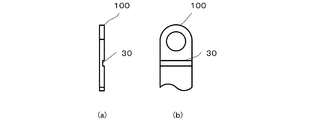
- FIG. 6 is a diagram showing an example of a terminal having a groove according to the present invention.
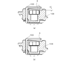
- FIG. 7 is a view showing a state in which a terminal having a groove according to the present invention is bent.
- FIG. 8 is a diagram showing attachment of the upper housing in the conventional terminal manufacturing method.
- FIG. 8 is a diagram showing attachment of the upper housing in the conventional terminal manufacturing method.
- FIG. 9 is a diagram illustrating a semiconductor module before terminal bending in a conventional terminal manufacturing method.
- (A) is the top view
- (b) is the side view.
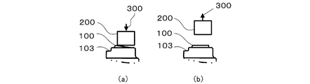
- FIG. 10 is a conceptual diagram illustrating a terminal bending step in a conventional terminal manufacturing method.
- (A) is a figure which shows the state which has bent the terminal
- (b) is a figure which shows the state after bending.
- FIG. 11 is a side view showing terminals of a semiconductor module manufactured by a conventional terminal manufacturing method.
- FIG. 8 A mode for carrying out the invention will be described with reference to the drawings.
- the general flow of the manufacturing process of the present invention is the same as that of the conventional method. That is, it is the same as that shown in FIGS.
- an external lead-out terminal 100 and a control terminal that are electrically connected and fixed to a circuit component such as a semiconductor element in the lower housing 102 are fixed to the lower housing 102 of the semiconductor module. It is the same that 101 is attached.
- the lower housing 102 is covered with the upper housing 103 having a through-hole through which the terminal 100 passes, the structure of the semiconductor module as shown in FIG. In FIG. 9, after the step shown in FIG.
- the circuit component includes an insulating substrate with a conductive pattern on which a semiconductor element is mounted and a heat dissipation base.
- the semiconductor module has a substantially rectangular parallelepiped shape.
- the bottom surface of the heat dissipation base is substantially flat, and forms one main surface S (see FIG. 8) of the semiconductor module.
- the upper housing 103 is attached to the semiconductor module such that its main surface S1 is parallel to one main surface S.
- the main surface S1 of the upper housing 103 is an upper surface.
- FIG. 1 is an explanatory diagram of a manufacturing method according to the present invention, and shows a state in which terminals are protruding above a casing.
- FIG. 2 is an explanatory view of the manufacturing method according to the present invention and is a view showing a terminal bending step. The terminal bending process of the present invention will be described with reference to FIGS.
- a through hole 103h through which the terminal 100 passes, a first fulcrum 1 formed at the opening of the through hole 103h, And a second fulcrum 2 formed at a position farther from the through hole 103h than the one fulcrum 1 is provided.
- the second fulcrum 2 is formed so as to protrude from the upper housing 103 with respect to the first fulcrum 1 and the bottom surface of the recess 3.
- FIG. 1 shows a state of the terminal 100 before starting to bend.
- a force 300 is applied to the terminal 100 by a bending jig (not shown), and the terminal 100 is bent.
- the terminal 100 bends inward, and the terminal 100 starts to bend with the fulcrum 1 serving as a fulcrum at first contacting the upper housing 103.
- FIG. 4A is a perspective view showing the relationship between the terminal 100 and the fulcrum 1.
- the terminal 100 is bent with the terminal 100 being bent by the first contact line 11 in contact with the upper housing 103 at the time of bending. This state is the first fulcrum. It is expressed as being bent with 1 as a fulcrum.
- the terminal 100 is bent, and then the bent portion with the second fulcrum 2 of the upper casing 103 as a fulcrum in contact with the upper casing 103 at the end as shown in FIG. 2B.
- the second fulcrum 2 is on the upper side of the first fulcrum 1 to about half the thickness of the terminal 100 to the same as the thickness of the terminal 100, and the horizontal direction between the first fulcrum 1 and the second fulcrum 2 is The distance is about the same as the thickness of the terminal 100 to about twice the thickness of the terminal 100.
- the terminal 100 is further bent, and is bent so that the tip end of the terminal 100 is displaced until it reaches the lower side at least by a length corresponding to the thickness of the terminal 100.
- the tip portion of the terminal 100 is bent so that the angle between the main surface of the upper housing 103 and the end portion of the terminal 100 is inclined downward at an angle ⁇ from the horizontal direction. It is done. This corresponds to bending of the end of the terminal 100 until the end of the terminal 100 is lowered by a length d from the position of the second fulcrum 2.
- the angle ⁇ is 1.3 ° to 5 °, as shown in FIG.
- the thickness of the terminal 100 used is about 0.6 mm to 2 mm.
- the length L of the part which becomes the external terminal of the bent terminal 100 is 10 mm to 30 mm.
- the length d corresponding to the range where the angle ⁇ is 1.3 ° to 5 ° is approximately 0.2 mm to 0.9 mm. is there.
- the length d corresponding to the range where the angle ⁇ is 1.3 ° to 5 ° is approximately 0.3 mm to 1.3 mm.
- the length d corresponding to the range in which the angle ⁇ is 1.3 ° to 5 ° is approximately 0.5 mm to 1.7 mm.
- the upper housing 103 is configured such that the range in which the bent terminal 100 passes in the bending process is the concave portion 3 so that the terminal 100 can be bent. This configuration is shown in FIG.
- the illustrated recess 3 is inclined with respect to the main surface of the upper housing 103. For the recess 3, if the gap between the tip of the terminal 100 and the upper housing 103 is D1, D1 is equal to or longer than the length d.
- the housing is made of so-called engineering plastic (engineering plastic) such as polyphenylin sulfide (PPS) or polybutylene terephthalate.
- the terminal 100 can be leveled even when there is a springback by bending the tip of the terminal 100 to the bottom of the recess so that it is inclined downward from the horizontal by ⁇ .
- the terminal 100 can be parallel to the main surface S ⁇ b> 1 of the upper housing 103.
- the bent terminal portion can be accommodated in a range of ⁇ 0.15 mm which is a high-precision specification of the height dimension from the mounting surface of the semiconductor module to the terminal.
- An important point in the present invention is that two fulcrum points are provided such as a first fulcrum and a second fulcrum. Compared to the case where bending is performed only at one fulcrum, the springback is dispersed at two fulcrums, the amount of springback is reduced, and it becomes easy to align the target horizontal position.
- the shape of the housing between the first fulcrum and the second fulcrum is a flat shape 20
- the shape may be a downward convex shape 21 as shown in FIG. 4C, or may be an upward convex shape 22 as shown in FIG. 4D.
- various shapes can be taken within the scope of the present invention, such as these shapes being steps.
- the number of terminals may be one in which a plurality of terminals are arranged in a row as described in FIG.
- the terminal may have a groove
- An example of the tip of this terminal is shown in FIG.
- FIG. 6A shows a side view of the tip portion
- FIG. 6B shows a front view of the tip portion.
- the terminal 100 has a groove 30 at the tip portion.
- tip part of FIG. 6 is provided with the hole for screw attachment.
- FIG. 7 shows a state where the terminal having the groove shown in FIG. 6 is bent.
- the casing is described as being separated as an upper casing and a lower casing, but the present invention can be applied regardless of the shape of the casing. According to the present invention, even when a terminal is processed by bending, the bent terminal can be leveled. As a result, the dimensional accuracy after terminal bending is increased and no correction work is required. Further, since the present invention can be applied if the product mold is partially changed, it can be easily applied to existing products.
Landscapes
- Manufacturing Of Electrical Connectors (AREA)
- Connections Arranged To Contact A Plurality Of Conductors (AREA)
Abstract
折り曲げ加工により形成される半導体モジュールの端子が傾いて高さばらつきを生じているものを改善した半導体モジュール用端子の折り曲げ方法である。 貫通孔、前記貫通孔の開口部に形成された第一の支点および前記第一の支点よりも前記貫通孔から離れた位置に形成された第二の支点を備える筐体と、端子とを用意する。前記貫通孔を貫通した前記端子を前記第一の支点を支点として折り曲げる。前記端子を前記第二の支点を支点として前記筐体の主面と略平行になるまで折り曲げる。さらに、前記第二の支点を支点として、前記筐体の主面に向かって前記端子の端部が少なくとも前記端子の厚さに相当する長さで変位するよう前記端子を折り曲げる。
Description
本発明は、ダイオード、サイリスタ、トランジスタモジュールなどの半導体モジュールにおける半導体モジュール用端子の折り曲げ方法に関する。
半導体モジュール製品において、外部接続用の端子を折り曲げて形成する製造方法は一般的には特許文献1の図面や特許文献2の図面に記載されたようなものが知られている。この端子の製造方法は、すなわちあらかじめその先端が外部端子としての形状に切断された導体が、内蔵回路と電気的接続がなされ、樹脂製のケース・ふた等の外装部材が取り付けられ、ナットを装填した後、板状の端子導体の先端部を折り曲げて端子を形成している。この端子の材料としては導電性の良い銅板や黄銅板が用いられる。
この端子の製造方法を、図8から図10を用いて工程ごとに説明する。図8は従来の端子製造方法における上側筐体の取り付けを示す図である。この図において、半導体モジュールの下側筐体102には、下側筐体102内部にある半導体素子などの回路構成部材と電気的接続がなされ固定された外部導出端子(以下、単に「端子」ともいう。)100及び制御端子101が取付けられている。これに端子100が貫通する孔を有する上側筐体103を被せると図9に示すような端子100の先端部が上側筐体103より上方に出ている構造が出来上がる。図9は、従来の端子製造方法における端子折り曲げ前の半導体モジュールを示す図である。図9(a)はその上面図であり、図9(b)は側面図である。図9では、図8に示す工程の後、端子にリードを締め付けるための六角ナット105が上側筐体103に挿入されている状態が示されている。この後、端子100の折り曲げ処理がなされる。
端子100の折り曲げ処理は、たとえば原理的には、図9に示す上側筐体から垂直に出ている端子100を、治具を用いて多少折り曲げた後、図10に示すように押圧治具200を用いて端子100を、端子治具100の先端が上側筐体103に接する程度まで押圧するものである。端子100の折り曲げ処理は、このほか、端子を押圧するローラーを用いることもできる。これは、図10においてローラーが紙面左手から右手に端子100を押圧しながら進行して端子を押圧するものである。これらのほか、端子曲げ加工を行う治具設備には、手動によるもの、自動で行うものなど種々の方法が用いられる。
また、外部接続用の端子を折り曲げて形成する方法には特許文献3のように、外部接続端子である電極を、筐体に設けた電極をはめこむための凹部をもうけて製造する方法も知られている。
また、外部接続用の端子を折り曲げて形成する方法には特許文献3のように、外部接続端子である電極を、筐体に設けた電極をはめこむための凹部をもうけて製造する方法も知られている。
また、特許文献4に開示された外部端子も知られている。この特許文献4に開示された端子の形成方法は、前述のように端子を筐体に組み付けてから折り曲げを行う方法とは異なり、あらかじめ折り曲げておいた電極を筐体に装着するものである。
本来外部導出端子は上側筐体の上面に平行になることを狙っているが、端子部材を曲げた後のそのスプリングバックによりその先端部が浮き上がってしまう。このスプリングバックによる端子先端部の浮き上がりを図10(b)及び図11に示す。特許文献1、2及び3に記載があるような端子の製造方法では、このような端子先端部の浮き上がりが発生しやすい。このため半導体モジュールを取りつけた面から端子上面までの高さ方向の寸法ばらつきが大きくなってしまう。たとえば複数の半導体モジュールを銅製などのブスバーにより並列接続する場合には、半導体モジュールの取り付け面から端子までの高さ寸法の精度が要求されるが、このスプリングバック効果による端子先端部の浮き上がりのために、その要求精度に対応できない場合が生じてしまう。この半導体モジュールの取り付け面から端子までの高さ寸法の要求精度は、例えば一般仕様の場合で±0.8mm、高精度仕様では±0.15mmである。このような高さ寸法の精度が要求される背景には、それぞれの端子とブスバーとの密着性確保、すなわち接触抵抗の低減、特定端子への応力集中による素子の内部破壊防止などがある。
スプリングバック効果による端子先端部の浮き上がりを抑えたり、浮き上がったものを修正するために、端子を強い力で曲げると上側筐体を破損させてしまう恐れがある。
特許文献4にあるように、あらかじめ折り曲げた端子を取り付ける方法もあるが、この方法ではインサート成形が出来ないため端子を強固に固定するに点に問題があるほか、既存品に適用しようとすると既存品の大幅な設計変更をしなくてはならずコスト上の問題も発生してしまう。
特許文献4にあるように、あらかじめ折り曲げた端子を取り付ける方法もあるが、この方法ではインサート成形が出来ないため端子を強固に固定するに点に問題があるほか、既存品に適用しようとすると既存品の大幅な設計変更をしなくてはならずコスト上の問題も発生してしまう。
本発明の課題は、スプリンクバックが起こっても、パワーモジュールを取り付ける面に取り付けた状態において、取り付け面より端子上面までの高さ寸法精度が確保できること、端子が取り付け面に対して傾かず平面となること、取り付け面と各端子面の平行度が容易に確保できること、さらにこれらの課題解決が安価で容易に行え、かつ大幅な構造変更を行うことなく既存品にも適用できることである。
本発明の半導体モジュール用端子の折り曲げ方法は、貫通孔、前記貫通孔の開口部に形成された第一の支点および前記第一の支点よりも前記貫通孔から離れた位置に形成された第二の支点を備える筐体と、端子とを用意し、
前記貫通孔を貫通した前記端子を前記第一の支点を支点として折り曲げ、
前記端子を前記第二の支点を支点として前記筐体の主面と略平行になるまで折り曲げ、
さらに、前記第二の支点を支点として、前記筐体の主面に向かって前記端子の端部が少なくとも前記端子の厚さに相当する長さで変位するよう前記端子を折り曲げることを特徴とする。
前記貫通孔を貫通した前記端子を前記第一の支点を支点として折り曲げ、
前記端子を前記第二の支点を支点として前記筐体の主面と略平行になるまで折り曲げ、
さらに、前記第二の支点を支点として、前記筐体の主面に向かって前記端子の端部が少なくとも前記端子の厚さに相当する長さで変位するよう前記端子を折り曲げることを特徴とする。
本発明の半導体モジュールは、回路構成部材が取り付けられた筐体と、該回路構成部材と電気的に接続して固定され、該筐体から上方に出ている端子と、を備えた半導体モジュールにおいて、
前記筐体は、端子が該筐体から上方で折り曲げられる際に最初に該筐体に接して支点となる第一の支点と、最後に該筐体に接して支点となる第二の支点と、前記端子が折り曲げられる範囲において凹部を有する構造であり、
前記端子は、前記筐体の第一の支点と第二の支点により折り曲げられて該端子の先端が前記筐体の主面と略平行になることを特徴とする。
前記筐体は、端子が該筐体から上方で折り曲げられる際に最初に該筐体に接して支点となる第一の支点と、最後に該筐体に接して支点となる第二の支点と、前記端子が折り曲げられる範囲において凹部を有する構造であり、
前記端子は、前記筐体の第一の支点と第二の支点により折り曲げられて該端子の先端が前記筐体の主面と略平行になることを特徴とする。
本発明によれば、折り曲げ加工された端子が半導体モジュールの上面に平行な平坦な構造となる。その結果、複数の半導体モジュールを並べて各半導体モジュールの端子をブスバーなどで接続する際に、各半導体モジュールの端子の高さが一様になりブスバーと半導体モジュールの端子間にあく隙間が小さく保たれ、ブスバーが各半導体モジュール面に平行に保たれる効果を有する。
発明を実施するための形態を、図を用いて説明する。本発明の製造工程のおおまかな流れは、従来の方法と同じである。すなわち、図8から図10に示すものと同じである。本発明においても図8において、半導体モジュールの下側筐体102には、下側筐体102内部にある半導体素子などの回路構成部材と電気的接続がなされ固定された外部導出端子100及び制御端子101が取付けられていることは同じである。下側筐体102に、端子100が貫通する貫通孔を有する上側筐体103を被せると図9に示すような半導体モジュールの構造が出来上がることも従来と同様である。図9において、図8に示す工程の後、端子100にリードを締め付けるための六角ナット105が挿入されている点も従来と同様である。この後、端子100の折り曲げ処理がなされるが、本発明が従来の方法と異なるのはこの端子折り曲げ処理である。
回路構成部材は、半導体素子が搭載された導電パターン付き絶縁基板と放熱ベースを備える。半導体モジュールは略直方体形状である。放熱ベースの底面は略平坦であり、半導体モジュールの一の主面S(図8参照)をなす。上側筐体103はその主面S1が一の主面Sに平行になるように半導体モジュールに取り付けられている。上側筐体103の主面S1は、上面である。
回路構成部材は、半導体素子が搭載された導電パターン付き絶縁基板と放熱ベースを備える。半導体モジュールは略直方体形状である。放熱ベースの底面は略平坦であり、半導体モジュールの一の主面S(図8参照)をなす。上側筐体103はその主面S1が一の主面Sに平行になるように半導体モジュールに取り付けられている。上側筐体103の主面S1は、上面である。
図1は、本発明に係る製造方法の説明図であって、端子が筐体の上方に出ている状態を示す図である。図2は、本発明に係る製造方法の説明図であって、端子折り曲げ工程を示す図である。これら図1及び図2を用いて本発明の端子折り曲げ工程を説明する。
半導体モジュールの上側筐体103においては、図1及び図2に示すように、端子100が貫通する貫通孔103hと、この貫通孔103hの開口部に形成された第一の支点1と、この第一の支点1よりも貫通孔103hから離れた位置に形成された第二の支点2とを備えている。第二の支点2は、第一の支点1および凹部3の底面に対して上部筐体103から突出するように形成されている。まず、端子を折り曲げる際に端子が上側筐体103と最初に接して支点となる上側筐体103の第一の支点1を支点として端子100が折り曲げられる。図1には端子100の折り曲げ開始前の状態が示されている。図2(a)に示すように折り曲げ治具(図示せず)により力300が端子100に作用して、端子100が曲がる。このとき端子100が内側に折れ曲がり上側筐体103に最初に接して支点となる支点1を支点として端子100は折れ曲がり始める。
ここで、図4(a)は端子100と支点1との関係を示す斜視図である。図4(a)に示すように端子100の折れ曲がりは、折れ曲がりの際に端子100が上側筐体103と接する第一の接触線11を支えとして折れ曲がるものであるが、この状態を第一の支点1を支点として折れ曲がると表現している。
引き続いて端子100が折り曲げられ、続いて図2(b)に示すように上側筐体103と最後に接して支点となる前記上側筐体103の第二の支点2を支点として、折り曲げられた部分がほぼ水平、すなわち、上部筐体103の主面S1と略平行になるまで折り曲げられる。第二の支点2は端子100の板厚の二分の一から端子100の板厚と同じ程度、第一の支点1より上側にあり、第一の支点1と第二の支点2の水平方向の距離は端子100の板厚と同じ程度から端子100の板厚の2倍程度である。
その後さらに端子100が折り曲げられ、端子100の端部先端が少なくとも端子100の厚さに相当する長さだけ下方に達するまで変位するよう折り曲げられる。好ましくは、図2(c)に示すように端子100の先端部分が、上部筐体103の主面と端子100の端部のなす角度として、水平方向からθの角度で下に傾く程度まで折り曲げられる。これは、端子100の端部先端が第二の支点2の位置よりも長さdだけ下がるまで折り曲げられることに対応する。角度θは1.3°から5°とすると図2(d)に示すようにスプリングバック後は、折り曲げられた端子がほぼ水平、すなわち、上部筐体103の主面S1と略平行となる。これらの折り曲げ工程は連続して行ってもよいし、また、各工程ごとに一旦停止してもよい。
用いられる端子100の板厚は0.6mmから2mm程度である。折り曲げられた端子100の外部端子となる部分の長さLは10mmから30mmである。たとえば、端子100の板厚が0.6mm、長さLが10mmの場合、角度θが1.3°から5°となる範囲に対応する長さdは、ほぼ0.2mmから0.9mmである。端子100の板厚が1mm、長さLが15mmの場合、角度θが1.3°から5°となる範囲に対応する長さdは、ほぼ0.3mmから1.3mmである。端子100の板厚が2mm、長さLが20mmの場合、角度θが1.3°から5°となる範囲に対応する長さdは、ほぼ0.5mmから1.7mmである。
用いられる端子100の板厚は0.6mmから2mm程度である。折り曲げられた端子100の外部端子となる部分の長さLは10mmから30mmである。たとえば、端子100の板厚が0.6mm、長さLが10mmの場合、角度θが1.3°から5°となる範囲に対応する長さdは、ほぼ0.2mmから0.9mmである。端子100の板厚が1mm、長さLが15mmの場合、角度θが1.3°から5°となる範囲に対応する長さdは、ほぼ0.3mmから1.3mmである。端子100の板厚が2mm、長さLが20mmの場合、角度θが1.3°から5°となる範囲に対応する長さdは、ほぼ0.5mmから1.7mmである。
このような端子100の折り曲げができるように上側筐体103は、その主面としての上面に、折り曲げられた端子100が折り曲げの過程で通過する範囲が凹部3となるよう構成されている。この構成を図5に示す。図示した凹部3は、上側筐体103の主面に対して傾斜している。この凹部3については、端子100の先端と上側筐体103との隙間をD1とすると、D1は長さd以上となる。なお筐体の材質は、ポリフェニリンサルファイド(PPS)、ポリブチレンテレフタレートなどのいわゆるエンジニアリングプラスチック(エンプラ)である。
このように端子100の先端部分が凹部の底面に向かってθだけ水平から下に傾く程度まで折り曲げられることによりスプリングバックがあっても端子を水平にすることができる。換言すれば端子100を上部筐体103の主面S1と平行にすることができる。
このような半導体モジュール用端子の折り曲げ方法によると折り曲げられた端子部分は、半導体モジュールの取り付け面から端子までの高さ寸法の高精度仕様である±0.15mmの範囲に収めることができる。
このような半導体モジュール用端子の折り曲げ方法によると折り曲げられた端子部分は、半導体モジュールの取り付け面から端子までの高さ寸法の高精度仕様である±0.15mmの範囲に収めることができる。
この発明で重要な点は、第一の支点と第二の支点というように二つの支点を設けた点である。単に一つの支点で折り曲げを行う場合に比べ、二つの支点でスプリングバックが分散され、スプリングバック量を小さく抑えられ、目標とする水平位置に位置合わせしやすくなる。
以上に述べた説明は、図4(a)及び(b)に示すように、第一の支点と第二の支点との間の筐体の形状は平坦形状20である場合であったが、この形状は図4(c)に示すように下に凸の形状21であっても良いし、図4(d)に示すように上に凸の形状22であっても良い。さらにこれらの形状が階段上であるなど本発明の範囲で様々な形状をとることができる。
以上に述べた説明では一つの端子について述べたが、端子の数は従来の技術として図9などで説明したように複数の端子が一列にあるものであっても良い。
また、端子は第一の支点及び第二の支点に対応する部分に端子が筐体に接する方向に平行な溝を有していても良い。この端子の先端部の例を図6に示す。図6(a)に先端部の側面図を、(b)に先端部の正面図を示す端子100は、先端部に溝30を有している。なお、図6の端子先端部分はねじ取付用の孔が設けられているものである。図6に示した溝を有する端子を、折り曲げた状態を図7に示す。
また、端子は第一の支点及び第二の支点に対応する部分に端子が筐体に接する方向に平行な溝を有していても良い。この端子の先端部の例を図6に示す。図6(a)に先端部の側面図を、(b)に先端部の正面図を示す端子100は、先端部に溝30を有している。なお、図6の端子先端部分はねじ取付用の孔が設けられているものである。図6に示した溝を有する端子を、折り曲げた状態を図7に示す。
以上の説明では、筐体は上側筐体と下側筐体というように分離した形で説明したが、本発明はこのような筐体の形状にかかわらず適用することができる。
本発明によれば、折り曲げにより端子を加工した場合でも折り曲げられた端子を水平にすることができる。その結果、端子曲げ後の寸法精度が上がり修正作業が不要となる。
また、製品の型を一部変更すれば本発明を適用できるので既存の製品への適用も容易に行うことができる。
本発明によれば、折り曲げにより端子を加工した場合でも折り曲げられた端子を水平にすることができる。その結果、端子曲げ後の寸法精度が上がり修正作業が不要となる。
また、製品の型を一部変更すれば本発明を適用できるので既存の製品への適用も容易に行うことができる。
1 第一の支点
2 第二の支点
3 筐体に設けられた凹部
11 第一の接触線
12 第二の接触線
20 第一の支点と第二の支点との間の筐体の平面形状
21 第一の支点と第二の支点との間の筐体の下に凸形状
22 第一の支点と第二の支点との間の筐体の上に凸形状
30 溝
100 端子
101 制御端子
102 下側筐体
103 上側筐体
104 止め穴
105 六角ナット
200 押圧治具
300 力
2 第二の支点
3 筐体に設けられた凹部
11 第一の接触線
12 第二の接触線
20 第一の支点と第二の支点との間の筐体の平面形状
21 第一の支点と第二の支点との間の筐体の下に凸形状
22 第一の支点と第二の支点との間の筐体の上に凸形状
30 溝
100 端子
101 制御端子
102 下側筐体
103 上側筐体
104 止め穴
105 六角ナット
200 押圧治具
300 力
Claims (9)
- 半導体モジュール用端子の折り曲げ方法であって、
貫通孔、前記貫通孔の開口部に形成された第一の支点および前記第一の支点よりも前記貫通孔から離れた位置に形成された第二の支点を備える筐体と、端子とを用意し、
前記貫通孔を貫通した前記端子を前記第一の支点を支点として折り曲げ、
前記端子を前記第二の支点を支点として前記筐体の主面と略平行になるまで折り曲げ、
さらに、前記第二の支点を支点として、前記筐体の主面に向かって前記端子の端部が少なくとも前記端子の厚さに相当する長さで変位するよう前記端子を折り曲げることを特徴とする半導体モジュール用端子の折り曲げ方法。 - 前記筐体の主面に前記第二の支点に隣接した凹部が形成されていて、前記端子を、前記第二の支点を支点として折り曲げた位置から、前記凹部の底面に向かって前記端子の端部が少なくとも前記端子の厚さに相当する長さで変位するよう折り曲げる請求項1に記載の半導体モジュール用端子の折り曲げ方法。
- 前記端子を前記第二の支点を支点として、前記端子の端部が前記筐体の主面と略平行になるように折り曲げる請求項2に記載の半導体モジュール用端子の折り曲げ方法。
- 前記端子を前記第二の支点を支点として、前記端子の端部が前記筐体の主面と略平行になるように折り曲げ、さらに前記主面と前記端子の端部のなす角度が1.3°から5°の範囲となるように折り曲げる請求項1に記載の半導体モジュール用端子の折り曲げ方法。
- 前記第一の支点と前記第二の支点との間の前記筐体の形状は平坦形状、上に凸形状乃至下に凸形状のいずれかの形状であることを特徴とする請求項1に記載の半導体モジュール用端子の折り曲げ方法。
- 前記第二の支点が、前記第一の支点および前記凹部の底面に対して前記筐体から突出するように形成されている請求項2に記載の半導体モジュール用端子の折り曲げ方法。
- 前記底面が前記筐体の主面に対して傾斜している請求項6に記載の半導体モジュール用端子の折り曲げ方法。
- 請求項1~7のいずれか1項に記載の半導体モジュール用端子の折り曲げ方法を含むことを特徴とする半導体モジュールの製造方法。
- 回路構成部材が取り付けられた筐体と、該回路構成部材と電気的に接続して固定され、該筐体から上方に出ている端子と、を備えた半導体モジュールにおいて、
前記筐体は、端子が該筐体から上方で折り曲げられる際に最初に該筐体に接して支点となる第一の支点と、最後に該筐体に接して支点となる第二の支点と、前記端子が折り曲げられる範囲において凹部を有する構造であり、
前記端子は、前記筐体の第一の支点と第二の支点により折り曲げられて該端子の先端が前記筐体の主面と略平行になることを特徴とする半導体モジュール。
Priority Applications (1)
| Application Number | Priority Date | Filing Date | Title |
|---|---|---|---|
| CN201390000610.0U CN204680664U (zh) | 2012-07-19 | 2013-07-18 | 半导体模块 |
Applications Claiming Priority (2)
| Application Number | Priority Date | Filing Date | Title |
|---|---|---|---|
| JP2012-160497 | 2012-07-19 | ||
| JP2012160497A JP2015173138A (ja) | 2012-07-19 | 2012-07-19 | 半導体モジュールの端子製造方法 |
Publications (1)
| Publication Number | Publication Date |
|---|---|
| WO2014014066A1 true WO2014014066A1 (ja) | 2014-01-23 |
Family
ID=49948888
Family Applications (1)
| Application Number | Title | Priority Date | Filing Date |
|---|---|---|---|
| PCT/JP2013/069546 Ceased WO2014014066A1 (ja) | 2012-07-19 | 2013-07-18 | 半導体モジュール用端子の折り曲げ方法 |
Country Status (3)
| Country | Link |
|---|---|
| JP (1) | JP2015173138A (ja) |
| CN (1) | CN204680664U (ja) |
| WO (1) | WO2014014066A1 (ja) |
Cited By (2)
| Publication number | Priority date | Publication date | Assignee | Title |
|---|---|---|---|---|
| CN114730742A (zh) * | 2020-06-16 | 2022-07-08 | 富士电机株式会社 | 半导体模块 |
| JP7539613B2 (ja) | 2019-06-28 | 2024-08-26 | オソン ディー アンド イー カンパニー リミテッド | Oledディスプレイ装置、およびそのバックカバーの製作方法 |
Families Citing this family (1)
| Publication number | Priority date | Publication date | Assignee | Title |
|---|---|---|---|---|
| JP6797505B1 (ja) * | 2020-03-23 | 2020-12-09 | 株式会社三社電機製作所 | 半導体装置 |
Citations (3)
| Publication number | Priority date | Publication date | Assignee | Title |
|---|---|---|---|---|
| JPH0472748A (ja) * | 1990-07-13 | 1992-03-06 | Mitsubishi Electric Corp | 半導体装置 |
| JPH0864722A (ja) * | 1994-08-26 | 1996-03-08 | Sanyo Electric Co Ltd | 混成集積回路装置 |
| JPH10256411A (ja) * | 1997-03-12 | 1998-09-25 | Sansha Electric Mfg Co Ltd | 電力用半導体モジュール |
-
2012
- 2012-07-19 JP JP2012160497A patent/JP2015173138A/ja active Pending
-
2013
- 2013-07-18 WO PCT/JP2013/069546 patent/WO2014014066A1/ja not_active Ceased
- 2013-07-18 CN CN201390000610.0U patent/CN204680664U/zh not_active Expired - Lifetime
Patent Citations (3)
| Publication number | Priority date | Publication date | Assignee | Title |
|---|---|---|---|---|
| JPH0472748A (ja) * | 1990-07-13 | 1992-03-06 | Mitsubishi Electric Corp | 半導体装置 |
| JPH0864722A (ja) * | 1994-08-26 | 1996-03-08 | Sanyo Electric Co Ltd | 混成集積回路装置 |
| JPH10256411A (ja) * | 1997-03-12 | 1998-09-25 | Sansha Electric Mfg Co Ltd | 電力用半導体モジュール |
Cited By (3)
| Publication number | Priority date | Publication date | Assignee | Title |
|---|---|---|---|---|
| JP7539613B2 (ja) | 2019-06-28 | 2024-08-26 | オソン ディー アンド イー カンパニー リミテッド | Oledディスプレイ装置、およびそのバックカバーの製作方法 |
| CN114730742A (zh) * | 2020-06-16 | 2022-07-08 | 富士电机株式会社 | 半导体模块 |
| CN114730742B (zh) * | 2020-06-16 | 2025-12-02 | 富士电机株式会社 | 半导体模块 |
Also Published As
| Publication number | Publication date |
|---|---|
| JP2015173138A (ja) | 2015-10-01 |
| CN204680664U (zh) | 2015-09-30 |
Similar Documents
| Publication | Publication Date | Title |
|---|---|---|
| US9390987B2 (en) | Semiconductor module including a terminal embedded in casing wall and bent over thick portion of lid | |
| TWI544705B (zh) | 蝶形彈簧連接器 | |
| US9362687B1 (en) | Electrical connector | |
| JP4943930B2 (ja) | 立体回路部品の取付構造 | |
| CN103053047A (zh) | 电连接装置和电连接元件以及蓄电池装置 | |
| JP2008211189A5 (ja) | ||
| JP2017054627A (ja) | ケーブル圧着端子実装体 | |
| US20100273297A1 (en) | Chip packaging method | |
| US20140246769A1 (en) | Semiconductor device and semiconductor device manufacturing method | |
| WO2014014066A1 (ja) | 半導体モジュール用端子の折り曲げ方法 | |
| US8770991B2 (en) | Fuse connection unit | |
| WO2014141990A1 (ja) | 基板補強構造 | |
| CN102044772B (zh) | 端子组合及其制造方法 | |
| JP6445932B2 (ja) | バスバー及びバスバーの製造方法 | |
| JP5245880B2 (ja) | 電力用半導体モジュールとその製造方法 | |
| US20170208688A1 (en) | Circuit assembly | |
| US10547152B2 (en) | Electrical connector assembly method | |
| US10566146B2 (en) | Electric double-layer capacitor including a terminal having a protruding portion in an exterior body thereof | |
| US9924598B2 (en) | Electronic control device and production method thereof | |
| CN104241914A (zh) | 连接器 | |
| JP5256518B2 (ja) | 半導体装置 | |
| JP6872953B2 (ja) | 発熱部品の固定構造および発熱部品の固定方法 | |
| CN218730927U (zh) | 芯片封装结构 | |
| JP2006059855A (ja) | チップ型電解コンデンサ及びその製造方法 | |
| US9252518B2 (en) | Electric connection structure of electronic component |
Legal Events
| Date | Code | Title | Description |
|---|---|---|---|
| WWE | Wipo information: entry into national phase |
Ref document number: 201390000610.0 Country of ref document: CN |
|
| 121 | Ep: the epo has been informed by wipo that ep was designated in this application |
Ref document number: 13820026 Country of ref document: EP Kind code of ref document: A1 |
|
| NENP | Non-entry into the national phase |
Ref country code: DE |
|
| 122 | Ep: pct application non-entry in european phase |
Ref document number: 13820026 Country of ref document: EP Kind code of ref document: A1 |
|
| NENP | Non-entry into the national phase |
Ref country code: JP |