WO2014007240A1 - 発光装置および発光装置の製造方法 - Google Patents
発光装置および発光装置の製造方法 Download PDFInfo
- Publication number
- WO2014007240A1 WO2014007240A1 PCT/JP2013/068118 JP2013068118W WO2014007240A1 WO 2014007240 A1 WO2014007240 A1 WO 2014007240A1 JP 2013068118 W JP2013068118 W JP 2013068118W WO 2014007240 A1 WO2014007240 A1 WO 2014007240A1
- Authority
- WO
- WIPO (PCT)
- Prior art keywords
- light emitting
- dam
- emitting device
- sealing resin
- light
- Prior art date
- Legal status (The legal status is an assumption and is not a legal conclusion. Google has not performed a legal analysis and makes no representation as to the accuracy of the status listed.)
- Ceased
Links
Images




Classifications
-
- H—ELECTRICITY
- H10—SEMICONDUCTOR DEVICES; ELECTRIC SOLID-STATE DEVICES NOT OTHERWISE PROVIDED FOR
- H10W—GENERIC PACKAGES, INTERCONNECTIONS, CONNECTORS OR OTHER CONSTRUCTIONAL DETAILS OF DEVICES COVERED BY CLASS H10
- H10W90/00—Package configurations
-
- H—ELECTRICITY
- H10—SEMICONDUCTOR DEVICES; ELECTRIC SOLID-STATE DEVICES NOT OTHERWISE PROVIDED FOR
- H10H—INORGANIC LIGHT-EMITTING SEMICONDUCTOR DEVICES HAVING POTENTIAL BARRIERS
- H10H20/00—Individual inorganic light-emitting semiconductor devices having potential barriers, e.g. light-emitting diodes [LED]
- H10H20/80—Constructional details
- H10H20/85—Packages
- H10H20/855—Optical field-shaping means, e.g. lenses
Definitions
- the present invention relates to a COB (Chip On Board) type light emitting device and a manufacturing method thereof.
- COB Chip On Board
- LEDs Light Emitting Diodes
- COB Chip On Board
- an annular dam ring 102 is disposed on a substrate 101, and an LED chip 103 is mounted on the substrate 101 inside the annular ring of the dam ring 102 to encapsulate resin. It is set as the structure sealed with 104.
- FIG. 9 in the COB type light emitting device 100, an annular dam ring 102 is disposed on a substrate 101, and an LED chip 103 is mounted on the substrate 101 inside the annular ring of the dam ring 102 to encapsulate resin. It is set as the structure sealed with 104.
- Patent Document 2 discloses a light emitting device in which an LED chip is mounted in a glass package.
- a convex portion is formed on the mounting surface of the LED chip in the glass package, and the LED chip is disposed in a recess surrounded by the convex portion and sealed with a sealing resin.
- Patent Document 2 discloses a configuration in which an optical component such as a glass lens is bonded with an adhesive on the upper surface of the convex portion, that is, above the LED chip (on the light emitting surface side).
- Patent Document 2 in a light emitting device in which an optical component such as a lens is arranged on the light emitting surface side of an LED chip, in order to obtain a desired optical effect such as a condensing function, the LED chip and the optical It is necessary to align the parts with the required accuracy.
- the optical component is displaced in a direction parallel to the light emitting surface of the light emitting device when the optical component is mounted.
- the present invention has been made in view of the above-described problems, and an object of the present invention is to easily and accurately attach an optical component in a light emitting device including an LED chip and an optical component such as a lens and a manufacturing method thereof. Another object of the present invention is to improve the light extraction efficiency in such a light emitting device.
- a light-emitting device of the present invention includes a substrate, a light-emitting element mounted on the substrate, a dam part formed on the substrate so as to surround a mounting region of the light-emitting element, A mounting region of the light emitting element surrounded by the dam part, a sealing resin for sealing the light emitting element, and an optical component mounted on the sealing resin, the dam part being the sealing It has a protruding portion that protrudes higher than the upper surface of the resin, and the outer peripheral edge of the optical component is aligned with the inner wall surface of the dam portion.
- the dam part has the protrusion part which protruded higher than the upper surface of sealing resin, and the outer periphery of an optical component is a dam ring by mounting an optical component on sealing resin.
- the optical component is positioned in contact with the inner wall surface. That is, the optical component can be positioned and arranged with respect to the light emitting element mounted on the substrate, and the optical component can be accurately attached without being displaced with respect to the light emitting element. Efficiency can be improved.
- the dam portion may be formed by overlapping a plurality of dams.
- the dam portion can have a desired shape, and further effects due to the shape of the dam portion can be obtained.
- the dam portion may be configured such that a taper is formed on the inner wall surface thereof.
- the dam portion can be provided with a function as a reflector that reflects the light emitted from the light emitting element toward the light emitting surface, and the light extraction efficiency of the light emitting device can be further improved.
- the dam portion includes a first dam portion in which the light emitting element is mounted inside a region surrounded by the dam portion, and the inside of the region is sealed with the sealing resin. And a second dam portion disposed outside the first dam portion with respect to the center of the region, and a region surrounded by the inner wall surface being larger than the region sealed with the sealing resin.
- the second dam portion is higher than the first dam portion, and the outer peripheral edge of the optical component is aligned with the inner wall surface of the second dam portion.
- region enclosed by the inner wall face of a 2nd dam part is sealed with sealing resin by forming a dam part into a 1st dam part and a 2nd dam part separately. It can be made larger than the region.
- an optical component size can be enlarged rather than the light emission surface size of sealing resin. As a result, the optical effect of the optical component is greater than when the optical component and the light emitting surface size are the same.
- a method of manufacturing a light emitting device includes a first step of mounting a light emitting element on the substrate, a second step of forming a dam portion disposed on the substrate, A third step of sealing the light emitting element with a sealing resin inside the region of the dam portion; and a fourth step of mounting an optical component on the sealing resin. It has a protruding portion that protrudes higher than the upper surface of the stop resin, and the outer peripheral edge of the optical component is mounted by being aligned with the inner wall surface of the dam portion.
- another method of manufacturing the light emitting device of the present invention includes a substrate, a light emitting element mounted on the substrate, a dam portion formed on the substrate so as to surround a mounting region of the light emitting element, and the dam.
- a second step of mounting an optical component on the resin, and the additional dam portion formed in the first step has a protruding portion protruding higher than the upper surface of the sealing resin, The outer peripheral edge of the optical component is positioned and mounted on the inner wall surface of the additional dam portion formed in the first step.
- the optical component when the additional dam portion is formed on the ready-made light emitting device and the optical component is mounted on the sealing resin, the optical component can be positioned by the additional dam portion.
- the light-emitting device of the present invention can be manufactured using an off-the-shelf light-emitting device, and in this case, the optical component can be attached with high accuracy without shifting from the light-emitting element, and the light extraction efficiency can be improved.
- a light emitting device can be obtained.
- the dam portion (or additional dam portion) can be formed by drawing a resin.
- the dam portion (or additional dam portion) can be formed by etching a resin film.
- the dam portion can be easily formed, and the additional dam portion can be easily formed with respect to the ready-made light emitting device. For this reason, it is possible to form a dam that matches the shape of the optical component to be mounted, such as a lens (circular, polygonal, etc.), and no mold is required, so the optical component is mounted at a specific position at low cost. can do.
- another light emitting device of the present invention is surrounded by a substrate, a light emitting element mounted on the substrate, a dam portion formed on the substrate so as to surround a mounting region of the light emitting element, and the dam portion.
- a mounting region of the light emitting element and a sealing resin for sealing the light emitting element, and the dam portion is formed by overlapping a plurality of dams, and a taper is formed on an inner wall surface thereof. It is characterized by being.
- the dam portion can be provided with a function as a reflector that reflects the light emitted from the light emitting element toward the light emitting surface, and the light extraction efficiency of the light emitting device can be improved.
- the optical component can be positioned and arranged with respect to the light-emitting element mounted on the substrate, and the optical component can be attached with high accuracy without shifting from the light-emitting element. There are effects such as. For this reason, in some cases, the light extraction efficiency from the light emitting device can be improved.
- FIG. 3A is a cross-sectional view showing an example of a method for forming a dam ring when the dam ring is formed of glass in the light emitting device of the first embodiment
- FIG. 4A to 4D are cross-sectional views illustrating an example of a method for forming a dam ring including a plurality of dams when the dam ring is formed of glass in the light emitting device of the first embodiment.
- FIG. 5 is a partial cross-sectional view illustrating an example of a lens bonding method in the light-emitting device of Embodiment 1. It is sectional drawing which shows schematic structure of the light-emitting device which concerns on Embodiment 2 of this invention. It is sectional drawing which shows schematic structure of the light-emitting device which concerns on Embodiment 3 of this invention. (A)-(c) is sectional drawing which shows the manufacturing method of the light-emitting device based on Embodiment 4 of this invention. It is sectional drawing which shows the structure of the conventional COB type light emission.
- FIG. 1 and 2 are cross-sectional views illustrating a schematic configuration of the light emitting device according to the first embodiment.
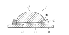
- the light emitting device 1 is a COB type light emitting device, in which an annular dam ring (dam part) 12 is arranged on a substrate 11, and an LED chip (light emitting element) 13 is attached to the substrate 11 inside the annular ring of the dam ring 12. It is mounted and sealed with a sealing resin 14. In addition, a lens (optical component) 15 is disposed on the sealing resin 14 and bonded with an adhesive.
- a connection electrode for mounting the LED chip 13 is formed on one surface of the substrate 11.
- the LED chip 13 is electrically connected to a connection electrode formed on the substrate 11 by, for example, a bonding wire (not shown). After the LED chip 13 is mounted, the dam ring 12 is formed at a predetermined position.
- the dam ring 12 can be formed from an insulating material such as resin or glass.
- an insulating material such as resin or glass.
- a dam resin is filled in a syringe, the syringe is moved (drawn) while discharging the dam resin, and then cured.
- a ring can be formed.
- the dam material is made of glass, there is a method in which an annular dam material is temporarily fixed at the predetermined position on the substrate 11 and then the dam material is fired, softened and melted and fixed on the substrate. .
- a glass paste can be partially potted for temporary fixing of the dam material.
- the sealing resin 14 is injected into the annular ring of the dam ring 12, and the LED chip 13 is sealed.
- the order of forming the dam ring 12 and mounting the LED chip 13 may be reversed depending on the method used to form the dam ring 12.
- the lens 15 When the sealing resin 14 is cured, the lens 15 is adhered thereon with an adhesive, and the light emitting device 1 is completed.
- the lens 15 may be mounted before the sealing resin 14 is cured, and the sealing resin 14 and the lens 15 may be bonded simultaneously by using the sealing resin 14 as an adhesive. In consideration of the positioning of the lens 15 in the vertical direction, it is preferable to adhere the lens 15 with an adhesive after the sealing resin 14 is cured.
- the dam material is a resin, for example, a silicone resin is used as the resin material, but a material having elasticity after curing is used. Therefore, when the dam material is made of resin, when the lens 15 is mounted, the lens 15 can be aligned without the dam ring giving an excessive load to the lens 15 or scratching. The same applies to the case where an optical component other than a lens is mounted, and also in an embodiment described later of a dam ring structure in which a plurality of dams are stacked.
- the upper surface (hereinafter referred to as a light emitting surface) 14a of the sealing resin 14 is formed to be lower than the upper surface of the dam ring 12.
- the dam ring 12 has a protruding portion protruding higher than the light emitting surface 14a.
- the protruding portion of the dam ring 12 is used for positioning when the lens 15 is attached.
- the lens 15 is disposed so as to contact the light emitting surface of the sealing resin 14. Further, the outer peripheral edge of the lens 15 is sized so as to coincide with the boundary between the light emitting surface of the sealing resin 14 and the dam ring 12. Thereby, when the lens 15 is placed on the light emitting surface of the sealing resin 14, the lens 15 can be positioned by the dam ring 12 by the outer peripheral edge of the lens 15 coming into contact with the inner wall surface of the dam ring 12.
- the dam material is a thixotropic resin, and its shape can be controlled before curing, so that a dam ring of any size and shape can be easily formed.
- the shape can be adjusted by changing the nozzle-substrate distance, nozzle diameter, discharge pressure, etc. during dam ring drawing.
- the dam material is cured by baking at 100 to 150 degrees, and is bonded to the substrate.
- FIG. 3 is a cross-sectional view showing an example of a method for forming a dam ring when the dam ring is formed of glass in the light emitting device of the first embodiment, and FIG. FIG. 3B shows the state after firing.
- the shape of the dam ring 12 changes somewhat with the subsequent firing relative to the shape when the dam material is temporarily fixed on the substrate 11.
- the dam ring 12 may be formed in a single stage (see FIG. 2), or may be formed by overlapping a plurality of dams (see FIG. 1).
- FIG. 1 shows an example in which a dam ring 12 is configured by overlapping two dams 12A and 12B.
- FIGS. 4A to 4D are cross-sectional views illustrating an example of a method for forming a dam ring including a plurality of dams when the dam ring is formed of glass in the light emitting device of the first embodiment.
- the dam ring 12 is formed by stacking a plurality of dams
- the dam ring 12 having a desired shape can be formed by repeating the temporary fixing and firing of the dam material by the number of dams to be stacked.
- the dam ring 12 having a desired shape can be formed by repeating the dam formation by drawing for the number of dams to be stacked.
- the light emitting device 1 includes the substrate 11, the LED chip 13 mounted on the substrate 11, and the dam ring formed on the substrate 11 so as to surround the mounting region of the light emitting element. 12, a mounting region of the LED chip 13 surrounded by the dam ring 12, a sealing resin 14 for sealing the LED chip 13, and a lens 15 mounted on the sealing resin 14.
- the dam ring 12 has a protruding portion that protrudes higher than the upper surface of the sealing resin 14, and the outer peripheral edge of the lens 15 is aligned with the inner wall surface of the dam ring 12.
- the inner wall surface of the dam ring 12 is used for positioning the lens 15, and the lens 15 is LED in a direction parallel to the substrate with respect to the light emitted from the sealing resin 14 (before the lens 15 is installed). It can be attached to the chip 13 with high accuracy without shifting, and the light extraction efficiency of the light emitting device 1 can be improved.
- the dam ring 12 can be formed of resin, glass or the like, and the structural design of the dam ring 12 becomes flexible.
- an optical component can be mounted at a desired position at low cost without using a mold or the like.
- the light emitting device 1 includes a first step of mounting the LED chip 13 on the substrate 11, a second step of forming the dam ring 12 disposed on the substrate 11, and the dam ring 12 It can be manufactured by a manufacturing method including a third step of sealing the LED chip 13 with the sealing resin 14 inside the region and a fourth step of mounting the lens 15 on the sealing resin 14.
- the lens 15 can be attached with high accuracy without shifting with respect to the light emitted from the sealing resin 14 (light before the lens 15 is installed), and a light emitting device with improved light extraction efficiency is obtained. Obtainable.
- FIG. 5 is a partial cross-sectional view showing an example of a method for adhering a lens in the light emitting device of the first embodiment.
- the adhesive 16 it is preferable to apply the adhesive 16 to the entire light emitting surface of the sealing resin 14 and the inner wall surface of the dam ring 12 to adhere the lens 15.
- a dedicated adhesive can be used, or the same material as the sealing resin 14 can be used. It is also possible to control the optical characteristics by changing the refractive index of the adhesive 16.
- the sealing resin 14 may contain a phosphor.
- the LED chip 13 is an LED chip that emits blue light, and white light is generated by mixing an appropriate amount of yellow phosphor (phosphor that absorbs blue light and generates yellow light) into the sealing resin 14.
- a light emitting device (white LED device) 1 can be obtained. It is good also as an LED device (for example, blue LED device which irradiates the light from a blue LED chip as it is) which irradiates the light from an LED chip as it is, without mixing a fluorescent substance in the sealing resin 14.
- the phosphor can be mixed not only in the sealing resin 14 but also in the adhesive 16.
- FIG. 6 is a cross-sectional view showing a schematic configuration of the light emitting device according to Embodiment 2 of the present invention.
- the dam ring is doubled. That is, instead of the dam ring 12 shown in FIG. 1, a first dam ring 21 and a second dam ring 22 are formed.
- the second dam ring 22 is disposed outside the first dam ring 21 so as to include the first dam ring 21 in its inner region. Thereby, the area surrounded by the inner wall surface of the second dam ring 22 is larger than the area sealed by the sealing resin 14 in the inner area of the first dam ring 21. Further, the second dam ring 22 is formed higher than the first dam ring 21.
- the first dam ring 21 and the second dam ring 22 are arranged apart from each other, but these dam rings may be arranged adjacent to each other.
- the LED chip 13 is arranged inside the ring of the first dam ring 21 and is sealed with a sealing resin 14. Further, a sealing resin 23 is injected into the annular shape of the second dam ring 22.
- the sealing resin 23 has a role of sealing the inside of the second dam ring 22 and bonding the lens 15.
- the lens 15 may be bonded onto the sealing resin 23 with an adhesive after the sealing resin 23 is cured.
- the second dam ring 22 has a protruding portion that protrudes higher than the sealing resin 23.
- this protruding portion is used for positioning the lens 15. For this reason, the lens 15 can be attached with high accuracy without shifting with respect to the light emitted from the sealing resin 23 (light before the lens 15 is installed), and the light extraction efficiency of the light emitting device 2 can be improved. .
- the light emitting device 2 can be expected to improve the light extraction efficiency by forming a double dam ring. This is because in the light emitting device 2, the lens effect can be increased by increasing the size of the lens 15 rather than the light emitting surface size of the sealing resin 14.
- the dam portion includes the first dam ring 21 in which the LED chip 13 is mounted inside the region and the inside of the region is sealed with the sealing resin 14.
- the second dam ring 22 is disposed outside the first dam ring 21 and the region surrounded by the inner wall surface thereof is larger than the region sealed with the sealing resin 14.
- the second dam ring 22 is formed higher than the first dam ring 21, and the outer peripheral edge of the lens 15 is in contact with the inner wall surface of the second dam ring 22.
- the first dam ring 21 and the second dam ring 22 may be formed at the same time after the LED chip 13 is mounted or before the mounting, but the formation timing is different as in the fourth embodiment to be described later. May be.
- Embodiment 3 For the light emitting device according to Embodiment 3, for convenience of explanation, members having the same functions as those in the drawings described in Embodiment 1 or 2 are denoted by the same reference numerals, and description thereof is omitted.
- FIG. 7 is a cross-sectional view showing a schematic configuration of the light emitting device according to Embodiment 3 of the present invention.
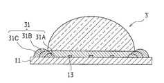
- the light emitting device 3 according to the third embodiment is characterized in that it has a dam ring formed by overlapping a plurality of dams and having a taper formed on the inner wall surface. That is, a dam ring 31 is formed instead of the dam ring 12 shown in FIG.
- the dam ring 31 has a function as a reflector that reflects light emitted from the LED chip 13 to the light emitting surface side by forming a taper on the inner wall surface thereof.
- the tapered dam ring 31 functions as a reflector that reflects the light emitted from the phosphor toward the light emitting surface in addition to the light emitted from the LED chip 13 when the phosphor is sealed. Have. Thereby, the light extraction efficiency of the light emitting device 3 can be further improved.
- the dam ring 31 shows an example in which the dam ring 31 is configured by overlapping three dams 31A to 31C.
- the number of stages of the dam ring 31 is not limited to three, and can be an arbitrary number.
- the dam ring 31 having a desired shape such as a tapered shape can be formed.
- the dam material is temporarily fixed and fired repeatedly for the number of dams to be stacked, so that a plurality of dams are stacked.
- a dam ring 31 can be formed.
- the dam ring 31 having a desired shape (tapered shape having a substantially constant inclination angle) is formed by appropriately setting the shape of the dam material when temporarily fixed, and the firing temperature and firing time during firing. can do.
- the dam ring 31 is desirably formed of a material having a high refractive index or a material having a higher refractive index than that of the sealing resin 14 in order to provide a function as a reflector.
- the light extraction efficiency can be improved only by the function of the dam ring 31 as a reflector. Therefore, such a configuration is also included in the scope of the present invention.
- Embodiment 4 For the light emitting device according to Embodiment 4, for convenience of explanation, members having the same functions as those in the drawings described in Embodiments 1 to 3 are denoted by the same reference numerals, and description thereof is omitted.
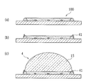
- the light emitting device 4 according to the fourth embodiment is such that a dam ring is additionally formed with respect to the ready-made light emitting device 100, and the lens 15 is positioned and bonded using the added dam ring.
- FIGS. 8 (a) to 8 (c) are cross-sectional views showing a method for manufacturing a light-emitting device according to Embodiment 4 of the present invention. That is, a dam ring (additional dam portion) 41 is additionally formed on the ready-made light emitting device 100 on which no optical component is mounted. Then, the light emitting device 4 according to the present embodiment can be manufactured by positioning and bonding the lens 15 using the added dam ring 41.
- the dam ring 41 is formed of a resin and the dam ring 41 is formed by the above-described resin drawing method.
- the structure including the substrate 11, the first dam ring 21, the LED chip 13, and the sealing resin 14 is a ready-made light emitting device, and the second dam ring 22 is an additional dam portion.
- the light emitting device of the present invention can be manufactured using the ready-made light emitting device 100.
- the first step of forming the additional dam portion on the substrate and the lens 15 on the sealing resin are mounted on the ready-made light emitting device 100. It can be manufactured by a manufacturing method including two steps. Further, the additional dam portion formed in the first step is formed to have a protruding portion that protrudes higher than the upper surface of the sealing resin, and the outer peripheral edge of the lens 15 is formed in the first step. Mounted with alignment on the inner wall of the dam.
- the ready-made light emitting device 100 seals the light emitting element inside the substrate, the dam portion arranged on the substrate, the light emitting element mounted on the substrate within the region of the dam portion, and the region of the dam portion. And a sealing resin.
- the optical component can be positioned by the additional dam part.
- the light emitting device of the present invention can be manufactured using a ready-made light emitting device, and at that time, the lens 15 can be attached with high accuracy without being displaced with respect to the LED chip 13, and the light extraction efficiency is improved. A light emitting device can be obtained.
- the present invention is not limited to the method described above, and the dam ring can also be formed by etching a resin film. That is, a resin film is formed on the entire surface of the substrate 11 to form a resin film, and a mask is formed on the resin film by using a photolithography technique so as to leave a dam ring formation region.
- the dam ring can be formed by removing the resin other than the formation region by etching.
- the inner wall surface of the dam ring can be matched with the outer periphery of the lens with good size. Further, as shown in Embodiment 4, this method can be suitably applied to the case where the lens 15 is mounted on the ready-made light emitting device 100 to manufacture the light emitting device of the present invention.
- the lens 15 as an optical component is mounted on the light emitting device by bonding.
- the present invention is not limited to this, and the lens may be directly formed on the sealing resin by resin casting.
- the lens can be directly formed by casting a highly thixotropic resin in the light emitting device in which the production stage from the formation of the dam ring to the sealing with the sealing resin is completed.
- the light emitting device in which the production stage from the formation of the dam ring to the sealing with the sealing resin has been completed is put in a mold such as a silicone resin (a mold in which the lens forming area is a space), and the inside of the space
- the lens can be directly formed on the sealing resin by pouring resin into the sealing resin.
- a dam ring can be used for positioning a lens formed by casting, and an optical component can be accurately mounted at a desired position.
- the region of the lens 15 and the region of the resin 23 shown in FIG. 6 are integrally formed using the same resin material. Can be molded.
- the optical component mounted on the light emitting device is a hemispherical lens
- the present invention is not limited to this, and any other optical component is mounted. May be.
- the optical component mounted on the light emitting device may be a glass bead, a microarray, a Fresnel lens, a reflector, or the like.
- the shape of the dam ring is an annular shape, but the present invention is not limited to this, and may be any other shape such as a rectangle or an ellipse.
- the dam ring (dam ring 12, 31, 41 or the second dam ring 22) used for positioning of the optical component has an appropriate shape for determining the position of the optical component to be mounted.
- the dam ring may be formed discontinuously.
- the portion related to the positioning of the optical component and not related to the blocking of the sealing resin 14 improves the accuracy of the mounting position of the optical component even if it is not continuously formed. be able to.
- the dam 12B shown in FIG. 1, the dam 31C shown in FIG. 7, the dam ring 41 shown in FIG. 8, etc. may be dam rings formed discontinuously.
- the dam ring for blocking the sealing resin 14 and the dam ring for positioning the optical component may be formed at different positions, and only the dam ring for positioning the optical component may be formed discontinuously. Good. In this case, the dam ring for positioning the optical component may be formed outside the dam ring for blocking the sealing resin 14.
Landscapes
- Led Device Packages (AREA)
Abstract
発光装置(1)は、基板(11)上にLEDチップ(13)を実装し、ダムリング(12)を配置し、封止樹脂(14)で封止している。さらに、封止樹脂(14)上にレンズ(15)を搭載している。ダムリング(12)の一部は封止樹脂(14)の上面よりも高く突出した突出部分を形成しており、レンズ(15)は、その外周縁がダムリングの(12)の内壁面と接触することにより位置決めされている。
Description
本発明は、COB(Chip On Board)タイプの発光装置およびその製造方法に関する。
近年、光源としてLED(Light Emitting Diode)を用いた種々の発光装置が開発されている。また、LEDを用いた発光装置では、LEDチップを基板上に直接実装して回路と接続し、樹脂封止するCOB(Chip On Board)タイプのものが広く知られている(特許文献1)。
図9に示すように、COBタイプの発光装置100では、基板101上に円環状のダムリング102を配置し、ダムリング102の円環内部でLEDチップ103を基板101に実装して封止樹脂104で封止する構成とされる。
また、特許文献2では、ガラスパッケージ内にLEDチップを搭載してなる発光装置が開示されている。特許文献2における発光装置の構成では、ガラスパッケージにおけるLEDチップの搭載面に凸部を形成し、その凸部で囲まれた窪み内にLEDチップを配置して封止樹脂で封止している。さらに、特許文献2では、凸部の上面、すなわちLEDチップの上方(光出射面側)において、ガラスレンズ等の光学部品を接着剤にて接着する構成が開示されている。
特許文献2に開示されているように、LEDチップの光出射面側にレンズ等の光学部品を配置する発光装置では、集光作用等の所望の光学効果を得るためには、LEDチップと光学部品とを要求される精度で位置合わせする必要がある。しかしながら、従来の技術では、光学部品の搭載の際に、発光装置の発光面に対して平行な方向にずれてしまう問題が発生していた。
また、特許文献1に示すようなCOBタイプの発光装置では、光学部品の搭載やダムリングの形状を制御することによって光の取り出し向上が期待できる。しかしながら、従来の発光装置ではそのような効果を十分に達成しているものは無かった。
本発明は、上記課題に鑑みてなされたものであり、LEDチップとレンズ等の光学部品とを備えた発光装置およびその製造方法において、光学部品を容易に精度良く取り付けられることを目的とする。また、そのような発光装置において、光の取り出し効率の向上を図ることをさらなる目的とする。
上記の課題を解決するために、本発明の発光装置は、基板と、前記基板に実装された発光素子と、前記基板上に前記発光素子の実装領域を取り囲むように形成されたダム部と、前記ダム部で取り囲まれた前記発光素子の実装領域および前記発光素子を封止する封止樹脂と、前記封止樹脂上に搭載された光学部品とを備えており、前記ダム部は前記封止樹脂の上面よりも高く突出した突出部分を有しており、前記光学部品外周縁が前記ダム部の内壁面で位置合わせされていることを特徴としている。
上記の構成によれば、ダム部が封止樹脂の上面よりも高く突出した突出部分を有しており、光学部品を封止樹脂上に搭載することによって、光学部品の外周縁がダムリングの内壁面と接触して、光学部品が位置決めされる。すなわち、光学部品を、基板に実装される発光素子に対して位置決めして配置することができ、光学部品を発光素子に対してずれることなく精度良く取り付けることができるため、発光装置からの光取り出し効率を向上させることができる。
また、本発明の発光装置では、前記ダム部は、複数段のダムを重ねて形成した構成とすることができる。
上記の構成によれば、ダム部に所望の形状を持たせることができ、ダム部の形状による更なる効果を得ることができる。
また、本発明の発光装置では、前記ダム部は、その内壁面にテーパが形成されている構成とすることができる。
上記の構成によれば、ダム部に発光素子からの出射光を発光面側に反射するリフレクタとしての機能を持たせることができ、発光装置の光取り出し効率をさらに向上させることができる。
また、本発明の発光装置では、前記ダム部は、前記ダム部で周囲を取り囲まれた領域内部に前記発光素子が実装され、その領域内部を前記封止樹脂で封止される第1ダム部と、前記領域の中心に対して前記第1ダム部よりも外側に配置され、その内壁面で囲まれる領域が前記封止樹脂にて封止される領域よりも大きい第2ダム部とを有しており、前記第2ダム部は、前記第1ダム部よりも高く、前記光学部品の外周縁が前記第2ダム部の内壁面で位置合わせされている構成とすることができる。
上記の構成によれば、ダム部を第1ダム部と第2ダム部とに分離して形成することにより、第2ダム部の内壁面で囲まれる領域が封止樹脂にて封止される領域よりも大きくなるようにすることができる。そして、光学部品の外周縁が第2ダム部の内壁面と接触するため、封止樹脂の発光面サイズよりも光学部品サイズを大きくすることができる。その結果、光学部品と発光面サイズとが同じである場合に比べて、光学部品における光学効果がより大きくなる。
上記の課題を解決するために、本発明の発光装置の製造方法は、発光素子を前記基板に実装する第1工程と、前記基板上に配置されるダム部を形成する第2工程と、前記ダム部の領域内部で前記発光素子を封止樹脂にて封止する第3工程と、前記封止樹脂上に光学部品を搭載する第4工程とを有しており、前記ダム部は前記封止樹脂の上面よりも高く突出した突出部分を有しており、前記光学部品の外周縁が前記ダム部の内壁面で位置合わせされて搭載されることを特徴としている。
上記の構成によれば、光学部品を発光素子に対してずれることなく精度良く取り付けることができ、光取り出し効率を向上させた発光装置を得ることができる。
また、本発明の発光装置の他の製造方法は、基板と、前記基板に実装された発光素子と、前記基板上に前記発光素子の実装領域を取り囲むように形成されたダム部と、前記ダム部で取り囲まれた前記発光素子の実装領域および前記発光素子を封止する封止樹脂とを備えた発光装置に対して、前記基板上に追加ダム部を形成する第1工程と、前記封止樹脂上に光学部品を搭載する第2工程とを有しており、前記第1工程にて形成される追加ダム部は前記封止樹脂の上面よりも高く突出した突出部分を有しており、前記光学部品の外周縁が前記第1工程にて形成される前記追加ダム部分の内壁面で位置合わせされて搭載されることを特徴としている。
上記の構成によれば、既製の発光装置に対して追加ダム部を形成し、封止樹脂上に光学部品を搭載する際には、追加ダム部によって光学部品を位置決めすることができる。これにより、既製の発光装置を用いて本発明の発光装置を製造することができ、その際に、光学部品を発光素子に対してずれることなく精度良く取り付けることができ、光取り出し効率を向上させた発光装置を得ることができる。
また、本発明の発光装置では、前記ダム部(もしくは追加ダム部)は、樹脂を描画することによって形成される構成とすることができる。また、本発明の発光装置では、前記ダム部(もしくは追加ダム部)は、樹脂膜をエッチングすることによって形成される構成とすることができる。
上記の構成によれば、ダム部の形成が容易であり、既製の発光装置に対して容易に追加ダム部を形成することもできる。このため、レンズなど搭載する光学部品の形状(円形、多角形など)に合わせたダムを形成することが可能であり、金型などを必要としないため、低コストで光学部品を特定位置に搭載することができる。
また、本発明の他の発光装置は、基板と、前記基板に実装された発光素子と、前記基板上に前記発光素子の実装領域を取り囲むように形成されたダム部と、前記ダム部で取り囲まれた前記発光素子の実装領域および前記発光素子を封止する封止樹脂とを備えており、前記ダム部は、複数段のダムを重ねて形成したものであり、その内壁面にテーパが形成されていることを特徴としている。
上記の構成によれば、ダム部に発光素子からの出射光を発光面側に反射するリフレクタとしての機能を持たせることができ、発光装置の光取り出し効率を向上させることができる。
本発明の発光装置およびその製造方法では、基板に実装される発光素子に対して光学部品を位置決めして配置することができ、光学部品を発光素子に対してずれることなく精度良く取り付けることができるといった効果を奏する。このため、場合によっては、発光装置からの光取り出し効率を向上させることができる。
以下、本発明の実施の形態について、図面を参照して詳細に説明する。
〔実施の形態1〕
図1,2は、本実施の形態1に係る発光装置の概略構成を示す断面図である。
図1,2は、本実施の形態1に係る発光装置の概略構成を示す断面図である。
発光装置1はCOBタイプの発光装置であって、基板11上に円環状のダムリング(ダム部)12を配置し、ダムリング12の円環内部でLEDチップ(発光素子)13を基板11に実装して封止樹脂14で封止している。また、封止樹脂14上にレンズ(光学部品)15を配置し、接着剤にて接着している。
基板11の一方の面には、LEDチップ13を実装するための接続電極が形成されている。LEDチップ13は、基板11に形成された接続電極と、例えばボンディングワイヤ(図示せず)によって電気接続される。LEDチップ13の実装後、ダムリング12が所定の位置に形成される。
ダムリング12は、樹脂やガラス等の絶縁性材料から形成することができる。ダムリング12の形成方法の一例としては、ダム材を樹脂とする場合には、シリンジなどにダム樹脂を充填し、ダム樹脂を吐出しながらシリンジを移動(描画)した後、硬化させることでダムリングを形成することができる。また、ダム材をガラスとするときには、円環形状のダム材を基板11上の上記所定の位置に仮止めした後、該ダム材を焼成して軟化溶融させて基板上に固着させる方法がある。上記ダム材の仮止めには、ガラスペーストを部分的にポッティングして用いることができる。
ダムリング12が形成されると、ダムリング12の円環内部に封止樹脂14が注入され、LEDチップ13が封止される。尚、ダムリング12の形成と、LEDチップ13の実装とは、ダムリング12の形成に用いる方法によっては、その順序を逆とすることもできる。
封止樹脂14が硬化すると、その上にレンズ15が接着剤にて接着され、発光装置1が完成する。あるいは、封止樹脂14の硬化前にレンズ15を搭載し、封止樹脂14を接着剤として用いることで、封止樹脂14の硬化とレンズ15の接着とを同時に行っても良い。尚、レンズ15の垂直方向の位置決めを考慮すれば、封止樹脂14の硬化後にレンズ15を接着剤にて接着することが好ましい。なお、ダム材を樹脂とした場合、樹脂の材料として、例えば、シリコーン樹脂を使用するが、硬化後に弾性を有するものを使用する。従って、ダム材を樹脂とした場合には、レンズ15を搭載する際に、ダムリングがレンズ15に対して過剰な負荷を与えたり、きずを与えることなくレンズ15の位置合わせができる。これは、レンズ以外の光学部品を搭載する場合、および複数段のダムを重ねてなるダムリング構造の後述する実施例でも同様である。
本実施の形態1に係る発光装置1では、封止樹脂14の上面(以下、発光面と称する)14aは、ダムリング12の上面よりも低くなるように形成される。このため、ダムリング12は、発光面14aよりも高く突出した突出部分を有する。そして、発光装置1では、このダムリング12の突出部分を、レンズ15を取り付ける際の位置決めに利用する。
具体的には、レンズ15は、封止樹脂14の発光面と接触するように配置される。また、レンズ15の外周縁は、封止樹脂14の発光面とダムリング12との境界に一致するようなサイズとされる。これにより、レンズ15を封止樹脂14の発光面に載置したときに、レンズ15の外周縁がダムリング12の内壁面と接触することにより、ダムリング12によってレンズ15を位置決めできる。
ダムリングを樹脂にて形成する場合は、ダム材をチクソ性のある樹脂とし、硬化前においてその形状をコントロールすることができるため、任意のサイズ・形状のダムリングを容易に形成できる。形状調整は、ダムリング描画時のノズル-基板距離やノズル径、吐出圧力などにより可能となる。ダムリングの描画後は、100~150度の焼成によりダム材が硬化し、また、基板と接着する。
図3は、本実施の形態1の発光装置において、ダムリングをガラスにて形成する場合の、ダムリングの形成方法の一例を示す断面図であって、図3(a)はダム材の焼成前、図3(b)は焼成後の状態を示している。ダムリング12は、ダム材を基板11上の仮止めした時の形状に対し、その後の焼成によって幾分形状が変化する。しかしながら、最初に仮止めする際のダム材の形状や、焼成時の焼成温度及び焼成時間を適切に設定することによって、焼成後のダムリング12において所望の形状を得ることが可能である。したがって、ダムリング12をレンズ15の位置決めに用いることは十分に可能となる。
ダムリング12は、1段で形成してもよく(図2参照)、あるいは、複数段のダムを重ねて形成しても良い(図1参照)。図1は、2段のダム12A,12Bを重ねてダムリング12を構成した例を示している。
図4(a)~(d)は、実施の形態1の発光装置において、ダムリングをガラスにて形成する場合の、複数段のダムからなるダムリングの形成方法の一例を示す断面図である。複数段のダムを重ねてダムリング12を形成する場合には、重ねられるダムの段数分だけ、ダム材の仮止めおよび焼成処理を繰り返せば、所望形状のダムリング12を形成することができる。ダムリングを樹脂にて形成する場合は、重ねられるダムの段数分だけ、描画によるダム形成を繰り返せば、所望形状のダムリング12を形成することができる。
このように、本実施の形態1に係る発光装置1は、基板11と、基板11に実装されたLEDチップ13と、基板11上に前記発光素子の実装領域を取り囲むように形成されたダムリング12と、ダムリング12で取り囲まれたLEDチップ13の実装領域およびLEDチップ13を封止する封止樹脂14と、封止樹脂14上に搭載されたレンズ15とを備えている。そして、ダムリング12は封止樹脂14の上面よりも高く突出した突出部分を有しており、レンズ15の外周縁がダムリング12の内壁面で位置合わせされている。
このため、ダムリング12の内壁面をレンズ15の位置決めに利用して、レンズ15を封止樹脂14から放出される光(レンズ15を設置する前の)に対して基板に平行な方向にLEDチップ13に対してずれることなく精度良く取り付けることができ、発光装置1の光取り出し効率を向上させることができる。また、ダムリング12は、樹脂やガラス等によって形成可能であり、ダムリング12の構造設計が柔軟となる。加えて、金型などを用いずに、低コストで所望位置に光学部品を搭載することが可能となる。
また、本実施の形態1に係る発光装置1は、LEDチップ13を基板11に実装する第1工程と、基板11上に配置されるダムリング12を形成する第2工程と、ダムリング12の領域内部でLEDチップ13を封止樹脂14にて封止する第3工程と、封止樹脂14上にレンズ15を搭載する第4工程とを含む製造方法にて製造することができる。
この製造方法によって、レンズ15を封止樹脂14から放出される光(レンズ15を設置する前の光)に対してずれることなく精度良く取り付けることができ、光取り出し効率を向上させた発光装置を得ることができる。
図5は、実施の形態1の発光装置において、レンズの接着方法の一例を示す部分断面図である。レンズ15を取り付ける際には、封止樹脂14の発光面全体およびダムリング12の内壁面に接着剤16を塗布して、レンズ15を接着することが好ましい。接着剤16については、専用の接着剤を用いることもできるし、封止樹脂14と同じ材料を用いることもできる。また、接着剤16の屈折率を変えることで光学特性をコントロールすることも可能である。
また、封止樹脂14には蛍光体が混入されていてもよい。例えば、LEDチップ13を青色光を照射するLEDチップとし、封止樹脂14に黄色蛍光体(青色光を吸収して黄色光を発生させる蛍光体)を適量混入させることで、白色光を発生させる発光装置(白色LED装置)1を得ることができる。封止樹脂14に蛍光体を混入せず、LEDチップからの光をそのまま照射するLED装置(例えば、青色LEDチップからの光をそのまま照射する青色LED装置)としてもよい。また、蛍光体は、封止樹脂14のみならず、接着剤16に混ぜることもできる。
〔実施の形態2〕
実施の形態2に係る発光装置について、説明の便宜上、実施の形態1にて説明した図面と同じ機能を有する部材については、同じ符号を付記し、その説明を省略する。
実施の形態2に係る発光装置について、説明の便宜上、実施の形態1にて説明した図面と同じ機能を有する部材については、同じ符号を付記し、その説明を省略する。
図6は、本発明の実施の形態2に係る発光装置の概略構成を示す断面図である。本実施の形態2に係る発光装置2は、ダムリングが二重に形成されている。すなわち、図1に示すダムリング12に代えて、第1ダムリング21と第2ダムリング22とが形成されている。第2ダムリング22は、その内部領域に第1ダムリング21を含むように第1ダムリング21よりも外側に配置されている。これにより、第2ダムリング22の内壁面で囲まれる領域は、第1ダムリング21の内部領域で封止樹脂14にて封止される領域よりも大きくなる。また、第2ダムリング22は、第1ダムリング21よりも高く形成されている。尚、図6では、第1ダムリング21と第2ダムリング22とは離間して配置されているが、これらのダムリングは隣接して配置されていても良い。
LEDチップ13は、第1ダムリング21の円環内部に配置され、封止樹脂14にて封止されている。また、第2ダムリング22の円環内部には封止樹脂23が注入されている。封止樹脂23は、第2ダムリング22の内部を封止するとともに、レンズ15を接着する役割を有する。あるいは、封止樹脂23を硬化させた後に、レンズ15を接着剤によって封止樹脂23上に接着する構成であっても良い。
本実施の形態2に係る発光装置2では、第2ダムリング22は、封止樹脂23よりも高く突出した突出部分を有する。そして、発光装置2では、この突出部分をレンズ15の位置決めに利用している。このため、レンズ15を封止樹脂23から放出される光(レンズ15を設置する前の光)対してずれることなく精度良く取り付けることができ、発光装置2の光取り出し効率を向上させることができる。
さらに、発光装置2では、ダムリングを二重に形成することで、光取り出し効率の向上が見込める。これは、発光装置2では、封止樹脂14の発光面サイズよりも、レンズ15のサイズを大きくすることで、レンズの効果を大きくすることができるためである。
このように、本実施の形態2に係る発光装置2では、ダム部は、その領域内部にLEDチップ13が実装され、その領域内部を封止樹脂14で封止される第1ダムリング21と、第1ダムリング21よりも外側に配置され、その内壁面で囲まれる領域が封止樹脂14にて封止される領域よりも大きくなるような第2ダムリング22とを有している。そして、第2ダムリング22は第1ダムリング21よりも高く形成されており、レンズ15は、その外周縁が第2ダムリング22の内壁面と接触している。これにより、封止樹脂14の発光面サイズよりもレンズ15のレンズサイズを大きくすることで、レンズ15における光学効果をより大きなものとすることができる。
尚、第1ダムリング21と第2ダムリング22とは、LEDチップ13の実装後もしくは実装前の段階で同時に形成しても良いが、後述する実施の形態4のように形成タイミングを異ならせても良い。
〔実施の形態3〕
実施の形態3に係る発光装置について、説明の便宜上、実施の形態1または2にて説明した図面と同じ機能を有する部材については、同じ符号を付記し、その説明を省略する。
実施の形態3に係る発光装置について、説明の便宜上、実施の形態1または2にて説明した図面と同じ機能を有する部材については、同じ符号を付記し、その説明を省略する。
図7は、本発明の実施の形態3に係る発光装置の概略構成を示す断面図である。本実施の形態3に係る発光装置3は、複数段のダムを重ねて形成され、内壁面にテーパが形成されたダムリングを有していることを特徴としている。すなわち、図1に示すダムリング12に代えて、ダムリング31が形成されている。ダムリング31は、その内壁面にテーパが形成されることによって、LEDチップ13からの出射光を発光面側に反射するリフレクタとしての機能を有している。また、テーパ形状のダムリング31は蛍光体が封止されている場合にはLEDチップ13からの射出光に加えて、蛍光体からの射出光を発光面側へと反射するリフレクタとしての機能を有している。これにより、発光装置3の光取り出し効率をさらに向上させることができる。
ダムリング31は、3段のダム31Aないし31Cを重ねてダムリング31を構成した例を示している。しかしながら、ダムリング31の段数は3段に限定されるものではなく、任意の段数とすることができる。
ダムリングを樹脂にて形成する場合は、ダムの描画条件(描画位置、ダムリング描画時のノズル-基板距離やノズル径、吐出圧力など)を適切に設定することで、ほぼ一定の傾斜角を有するテーパ形状など、所望形状のダムリング31を形成することができる。またダムリングをガラスにて形成する場合は、図4にて説明したように、重ねられるダムの段数分だけ、ダム材の仮止めおよび焼成処理を繰り返すことで、複数段のダムを重ねてなるダムリング31を形成することができる。このとき、最初に仮止めする際のダム材の形状や、焼成時の焼成温度及び焼成時間を適切に設定すれば、所望形状(ほぼ一定の傾斜角を有するテーパ形状)のダムリング31を形成することができる。
また、ダムリング31は、リフレクタとしての機能を持たせるため、高反射率の材料もしくは封止樹脂14よりも屈折率の大きい材料にて形成されることが望ましい。
尚、本実施の形態3に係る発光装置では、封止樹脂14上に光学部品15を配置しない構成であっても、ダムリング31におけるリフレクタとしての機能のみで光取り出し効率を向上させることができるため、そのような構成も本発明の範囲に含まれる。
〔実施の形態4〕
実施の形態4に係る発光装置について、説明の便宜上、実施の形態1~3にて説明した図面と同じ機能を有する部材については、同じ符号を付記し、その説明を省略する。
実施の形態4に係る発光装置について、説明の便宜上、実施の形態1~3にて説明した図面と同じ機能を有する部材については、同じ符号を付記し、その説明を省略する。
本実施の形態4に係る発光装置4は、既製の発光装置100に対して、ダムリングを追加形成し、この追加されたダムリングを利用してレンズ15を位置決めして接着するものである。
図8(a)~(c)は、本発明の実施の形態4に係る発光装置の製造方法を示す断面図である。すなわち、光学部品が搭載されていない既製の発光装置100に対し、ダムリング(追加ダム部)41を追加形成する。そして、追加されたダムリング41を利用してレンズ15を位置決めして接着することで本実施の形態に係る発光装置4を製造できる。
ダムリング41を追加形成する場合には、ダムリングを樹脂にて形成し、上述した樹脂の描画方法によってダムリング41を形成することが好ましい。
また、図6に示す発光装置2においても、基板11、第1ダムリング21、LEDチップ13、および封止樹脂14からなる構成までを既製の発光装置とし、第2ダムリング22を追加ダム部として形成すれば、既製の発光装置100を用いて本発明の発光装置を製造することができる。
このように、本実施の形態4に係る発光装置4は、既製の発光装置100に対して、基板上に追加ダム部を形成する第1工程と、封止樹脂上にレンズ15を搭載する第2工程とを含む製造方法にて製造することができる。また、第1工程にて形成される追加ダム部は封止樹脂の上面よりも高く突出した突出部分を有するように形成され、レンズ15の外周縁が前記第1工程にて形成される前記追加ダム部分の内壁面で位置合わせされて搭載される。ここで、既製の発光装置100は、基板と、基板上に配置されたダム部と、ダム部の領域内部で基板に実装される発光素子と、ダム部の領域内部で発光素子を封止する封止樹脂とを有する。
これにより、既製の発光装置に対して追加ダム部を形成し、封止樹脂上にレンズ15を搭載する際には、この追加ダム部によって光学部品を位置決めすることができる。これにより、既製の発光装置を用いて本発明の発光装置を製造することができ、その際に、レンズ15をLEDチップ13に対してずれることなく精度良く取り付けることができ、光取り出し効率を向上させた発光装置を得ることができる。
〔変形例〕
ダムリングの形成方法として、本発明は上記した方法に限定されるものではなく、ダムリングは樹脂膜をエッチングすることによって形成することもできる。すなわち、基板11の全面に樹脂を塗布して樹脂膜を形成し、この樹脂膜上にフォトリソグラフィ技術を用いてダムリングの形成領域を残したマスクを形成し、このマスクを用いてダムリングの形成領域以外の樹脂をエッチングで除去することによってダムリングを形成することができる。この方法では、ダムリング内壁面をレンズ外周にサイズ良く合わせることができる。また、この方法は、実施の形態4で示したように、既製の発光装置100に対してレンズ15を搭載し、本発明の発光装置を製造する場合にも好適に適用することができる。
ダムリングの形成方法として、本発明は上記した方法に限定されるものではなく、ダムリングは樹脂膜をエッチングすることによって形成することもできる。すなわち、基板11の全面に樹脂を塗布して樹脂膜を形成し、この樹脂膜上にフォトリソグラフィ技術を用いてダムリングの形成領域を残したマスクを形成し、このマスクを用いてダムリングの形成領域以外の樹脂をエッチングで除去することによってダムリングを形成することができる。この方法では、ダムリング内壁面をレンズ外周にサイズ良く合わせることができる。また、この方法は、実施の形態4で示したように、既製の発光装置100に対してレンズ15を搭載し、本発明の発光装置を製造する場合にも好適に適用することができる。
また、上記説明では、光学部品であるレンズ15を接着によって発光装置に搭載していた。しかしながら、本発明はこれに限定されるものではなく、レンズは樹脂注型成形によって封止樹脂上に直接形成しても良い。この場合、ダムリングが形成されて封止樹脂による封止までの製造段階が終了している発光装置にチクソ性の高い樹脂を注型することによりレンズを直接形成することができる。あるいは、ダムリングが形成されて封止樹脂による封止までの製造段階が終了している発光装置を、シリコーン樹脂等の型(レンズ形成領域が空間となっている型)に入れ、その空間内に樹脂を流し込んで封止樹脂上にレンズを直接形成することができる。
この方法によっても、注型成形によって形成されるレンズの位置決めにダムリングを利用することができ、所望位置に精度良く光学部品を搭載することができる。
尚、実施の形態2の構成において、レンズ15の成形に樹脂注型成形を用いる場合には、図6に示すレンズ15の領域と樹脂23の領域とを、同一の樹脂材料を用いて一体的に成形することができる。
また、上記説明では、発光装置に搭載される光学部品が半球レンズである場合を例示したが、本発明はこれに限定されるものではなく、他の任意の光学部品が搭載されるものであっても良い。例えば、発光装置に搭載される光学部品は、ガラスビーズ、マイクロアレイ、フレネルレンズ、リフレクタ等であっても良い。
また、上記説明では、ダムリングの形状を円環状としたが、本発明はこれに限定されるものではなく、矩形や楕円など他の任意の形状であっても良い。但し、光学部品の位置決めに利用されるダムリング(ダムリング12,31,41または第2ダムリング22)は、搭載される光学部品の位置を決めるのに適切な形状とされる。
また、上記説明では、ダムリングは、連続的に形成される例を説明したが、本発明はこれに限定されるものではなく、不連続に形成されるものであっても良い。特に、光学部品の位置決めに関与する部分であって、封止樹脂14の堰き止めに関与しない部分については、連続的に形成されているものでなくても光学部品の取り付け位置の精度を向上させることができる。例えば、図1に示すダム12B,図7に示すダム31C,図8に示すダムリング41等は、不連続に形成されるダムリングであってもよい。
あるいは、封止樹脂14の堰き止め用のダムリングと光学部品の位置決め用のダムリングとを異なる位置に形成し、光学部品の位置決め用のダムリングのみを不連続に形成する構成であってもよい。この場合、光学部品の位置決め用のダムリングは、封止樹脂14の堰き止め用のダムリングの外側に形成されてもよい。
本発明は上述した各実施形態に限定されるものではなく、請求項に示した範囲で種々の変更が可能であり、異なる実施形態にそれぞれ開示された技術的手段を適宜組み合わせて得られる実施形態についても本発明の技術的範囲に含まれる。
1,2,3,4 発光装置
11 基板
12,31 ダムリング(ダム部)
13 LEDチップ(発光素子)
14,23 封止樹脂
15 レンズ(光学部品)
21 第1ダムリング(第1ダム部)
22 第2ダムリング(第2ダム部,追加ダム部)
41 ダムリング(追加ダム部)
11 基板
12,31 ダムリング(ダム部)
13 LEDチップ(発光素子)
14,23 封止樹脂
15 レンズ(光学部品)
21 第1ダムリング(第1ダム部)
22 第2ダムリング(第2ダム部,追加ダム部)
41 ダムリング(追加ダム部)
Claims (11)
- 基板と、
前記基板に実装された発光素子と、
前記基板上に前記発光素子の実装領域を取り囲むように形成されたダム部と、
前記ダム部で取り囲まれた前記発光素子の実装領域および前記発光素子を封止する封止樹脂と、
前記封止樹脂上に搭載された光学部品とを備えており、
前記ダム部は前記封止樹脂の上面よりも高く突出した突出部分を有しており、前記光学部品外周縁が前記ダム部の内壁面で位置合わせされていることを特徴とする発光装置。 - 請求項1に記載の発光装置において、
前記ダム部は、複数段のダムを重ねて形成したものであることを特徴とする発光装置。 - 請求項2に記載の発光装置において、
前記ダム部は、その内壁面にテーパが形成されていることを特徴とする発光装置。 - 請求項1に記載の発光装置において、
前記ダム部は、
前記ダム部で周囲を取り囲まれた領域内部に前記発光素子が実装され、その領域内部を前記封止樹脂で封止される第1ダム部と、
前記領域の中心に対して前記第1ダム部よりも外側に配置され、その内壁面で囲まれる領域が前記封止樹脂にて封止される領域よりも大きい第2ダム部とを有しており、
前記第2ダム部は、前記第1ダム部よりも高く、
前記光学部品の外周縁が前記第2ダム部の内壁面と位置合わせされていることを特徴とする発光装置。 - 発光素子を前記基板に実装する第1工程と、
前記基板上に配置されるダム部を形成する第2工程と、
前記ダム部の領域内部で前記発光素子を封止樹脂にて封止する第3工程と、
前記封止樹脂上に光学部品を搭載する第4工程とを有しており、
前記ダム部は前記封止樹脂の上面よりも高く突出した突出部分を有しており、
前記光学部品の外周縁が前記ダム部の内壁面で位置合わせされて搭載されることを特徴とする発光装置の製造方法。 - 基板と、前記基板に実装された発光素子と、前記基板上に前記発光素子の実装領域を取り囲むように形成されたダム部と、前記ダム部で取り囲まれた前記発光素子の実装領域および前記発光素子を封止する封止樹脂とを備えた発光装置に対して、前記基板上に追加ダム部を形成する第1工程と、
前記封止樹脂上に光学部品を搭載する第2工程とを有しており、
前記第1工程にて形成される追加ダム部は前記封止樹脂の上面よりも高く突出した突出部分を有しており、
前記光学部品の外周縁が前記第1工程にて形成される前記追加ダム部分の内壁面で位置合わせされて搭載されることを特徴とする発光装置の製造方法。 - 請求項5に記載の発光装置の製造方法において、
前記第2工程にて形成される前記ダム部は、樹脂を描画することによって形成されることを特徴とする発光装置の製造方法。 - 請求項6に記載の発光装置の製造方法において、
前記第1工程にて形成される前記追加ダム部は、樹脂を描画することによって形成されることを特徴とする発光装置の製造方法。 - 請求項5に記載の発光装置の製造方法において、
前記第2工程にて形成される前記ダム部は、樹脂膜をエッチングすることによって形成されることを特徴とする発光装置の製造方法。 - 請求項6に記載の発光装置の製造方法において、
前記第1工程にて形成される前記追加ダム部は、樹脂膜をエッチングすることによって形成されることを特徴とする発光装置の製造方法。 - 基板と、
前記基板に実装された発光素子と、
前記基板上に前記発光素子の実装領域を取り囲むように形成されたダム部と、
前記ダム部で取り囲まれた前記発光素子の実装領域および前記発光素子を封止する封止樹脂とを備えており、
前記ダム部は、複数段のダムを重ねて形成したものであり、その内壁面にテーパが形成されていることを特徴とする発光装置。
Applications Claiming Priority (2)
| Application Number | Priority Date | Filing Date | Title |
|---|---|---|---|
| JP2012-152759 | 2012-07-06 | ||
| JP2012152759 | 2012-07-06 |
Publications (1)
| Publication Number | Publication Date |
|---|---|
| WO2014007240A1 true WO2014007240A1 (ja) | 2014-01-09 |
Family
ID=49881995
Family Applications (1)
| Application Number | Title | Priority Date | Filing Date |
|---|---|---|---|
| PCT/JP2013/068118 Ceased WO2014007240A1 (ja) | 2012-07-06 | 2013-07-02 | 発光装置および発光装置の製造方法 |
Country Status (1)
| Country | Link |
|---|---|
| WO (1) | WO2014007240A1 (ja) |
Cited By (5)
| Publication number | Priority date | Publication date | Assignee | Title |
|---|---|---|---|---|
| JP2016115897A (ja) * | 2014-12-18 | 2016-06-23 | シチズン電子株式会社 | 発光装置及びその製造方法 |
| JP2017118088A (ja) * | 2015-12-21 | 2017-06-29 | ルーメンス カンパニー リミテッド | Ledモジュール |
| US10193032B2 (en) | 2016-09-30 | 2019-01-29 | Nichia Corporation | Method for manufacturing light emitting device |
| JP2022104258A (ja) * | 2020-12-28 | 2022-07-08 | 三菱電機株式会社 | 表示ユニット、表示装置、及び表示ユニットの製造方法 |
| WO2025082668A1 (en) * | 2023-10-17 | 2025-04-24 | Ams-Osram International Gmbh | Device and method for producing a device |
Citations (4)
| Publication number | Priority date | Publication date | Assignee | Title |
|---|---|---|---|---|
| JPH0983018A (ja) * | 1995-09-11 | 1997-03-28 | Nippon Denyo Kk | 発光ダイオードユニット |
| JP2002543594A (ja) * | 1999-04-22 | 2002-12-17 | オスラム オプト セミコンダクターズ ゲゼルシャフト ミット ベシュレンクテル ハフツング | レンズ付led光源 |
| JP2008512867A (ja) * | 2004-09-10 | 2008-04-24 | ソウル セミコンダクター カンパニー リミテッド | 多重モールド樹脂を有する発光ダイオードパッケージ |
| JP2012094611A (ja) * | 2010-10-26 | 2012-05-17 | Panasonic Corp | 照明装置 |
-
2013
- 2013-07-02 WO PCT/JP2013/068118 patent/WO2014007240A1/ja not_active Ceased
Patent Citations (4)
| Publication number | Priority date | Publication date | Assignee | Title |
|---|---|---|---|---|
| JPH0983018A (ja) * | 1995-09-11 | 1997-03-28 | Nippon Denyo Kk | 発光ダイオードユニット |
| JP2002543594A (ja) * | 1999-04-22 | 2002-12-17 | オスラム オプト セミコンダクターズ ゲゼルシャフト ミット ベシュレンクテル ハフツング | レンズ付led光源 |
| JP2008512867A (ja) * | 2004-09-10 | 2008-04-24 | ソウル セミコンダクター カンパニー リミテッド | 多重モールド樹脂を有する発光ダイオードパッケージ |
| JP2012094611A (ja) * | 2010-10-26 | 2012-05-17 | Panasonic Corp | 照明装置 |
Cited By (5)
| Publication number | Priority date | Publication date | Assignee | Title |
|---|---|---|---|---|
| JP2016115897A (ja) * | 2014-12-18 | 2016-06-23 | シチズン電子株式会社 | 発光装置及びその製造方法 |
| JP2017118088A (ja) * | 2015-12-21 | 2017-06-29 | ルーメンス カンパニー リミテッド | Ledモジュール |
| US10193032B2 (en) | 2016-09-30 | 2019-01-29 | Nichia Corporation | Method for manufacturing light emitting device |
| JP2022104258A (ja) * | 2020-12-28 | 2022-07-08 | 三菱電機株式会社 | 表示ユニット、表示装置、及び表示ユニットの製造方法 |
| WO2025082668A1 (en) * | 2023-10-17 | 2025-04-24 | Ams-Osram International Gmbh | Device and method for producing a device |
Similar Documents
| Publication | Publication Date | Title |
|---|---|---|
| KR101111256B1 (ko) | Led 리드 프레임 패키지, 이를 이용한 led 패키지 및 상기 led 패키지의 제조 방법 | |
| CN101278410B (zh) | 利用分配的密封剂的半导体发光器件的封装及其封装方法 | |
| US20150380616A1 (en) | Batwing led with remote phosphor configuration | |
| KR101923588B1 (ko) | 발광장치, 그 제조방법 및 조명장치 | |
| CN101937962A (zh) | 一种led封装结构及其封装方法 | |
| US20050212405A1 (en) | Semiconductor light emitting devices including flexible film having therein an optical element, and methods of assembling same | |
| US20120098006A1 (en) | Light emitting diode package with photoresist reflector and method of manufacturing | |
| WO2014007240A1 (ja) | 発光装置および発光装置の製造方法 | |
| CN104465941A (zh) | 发光器件及其制造方法 | |
| KR101575366B1 (ko) | 발광소자 패키지 | |
| US9209338B2 (en) | Optical device with through-hole cavity | |
| JP5334123B2 (ja) | 半導体発光装置、半導体発光装置アセンブリ、および半導体発光装置の製造方法 | |
| JP7044978B2 (ja) | 発光装置及び照明装置、並びに、それらの製造方法 | |
| JP6510256B2 (ja) | Ledモジュールの製造方法 | |
| CN112531089A (zh) | 发光装置、照明装置以及其制造方法 | |
| JP2008187212A (ja) | 面実装型発光素子 | |
| TW201401566A (zh) | 發光二極體的封裝方法 | |
| JP5702481B2 (ja) | 発光装置およびその製造方法 | |
| KR101984897B1 (ko) | 발광 다이오드 패키지 및 그 제조 방법 | |
| TW201829649A (zh) | 製造發光二極體器件的方法及製造的發光二極體器件 | |
| CN103165763B (zh) | 发光二极管的制造方法 | |
| KR101724703B1 (ko) | 렌즈 패턴이 형성된 화이트 발광용 칩 패키지 | |
| KR20160059450A (ko) | 몰드 기판, 패키지 구조체 및 이들의 제조 방법 | |
| CN105845790A (zh) | 一种倒装led芯片的封装方法及封装槽模具 | |
| TW201427096A (zh) | 發光二極體封裝結構之製造方法 |
Legal Events
| Date | Code | Title | Description |
|---|---|---|---|
| 121 | Ep: the epo has been informed by wipo that ep was designated in this application |
Ref document number: 13813601 Country of ref document: EP Kind code of ref document: A1 |
|
| NENP | Non-entry into the national phase |
Ref country code: DE |
|
| 122 | Ep: pct application non-entry in european phase |
Ref document number: 13813601 Country of ref document: EP Kind code of ref document: A1 |
|
| NENP | Non-entry into the national phase |
Ref country code: JP |