WO2014007091A1 - 画像形成装置 - Google Patents
画像形成装置 Download PDFInfo
- Publication number
- WO2014007091A1 WO2014007091A1 PCT/JP2013/067202 JP2013067202W WO2014007091A1 WO 2014007091 A1 WO2014007091 A1 WO 2014007091A1 JP 2013067202 W JP2013067202 W JP 2013067202W WO 2014007091 A1 WO2014007091 A1 WO 2014007091A1
- Authority
- WO
- WIPO (PCT)
- Prior art keywords
- charging roller
- charging
- voltage
- photosensitive member
- potential
- Prior art date
- Legal status (The legal status is an assumption and is not a legal conclusion. Google has not performed a legal analysis and makes no representation as to the accuracy of the status listed.)
- Ceased
Links
Images





Classifications
-
- G—PHYSICS
- G03—PHOTOGRAPHY; CINEMATOGRAPHY; ANALOGOUS TECHNIQUES USING WAVES OTHER THAN OPTICAL WAVES; ELECTROGRAPHY; HOLOGRAPHY
- G03G—ELECTROGRAPHY; ELECTROPHOTOGRAPHY; MAGNETOGRAPHY
- G03G15/00—Apparatus for electrographic processes using a charge pattern
- G03G15/80—Details relating to power supplies, circuits boards, electrical connections
-
- G—PHYSICS
- G03—PHOTOGRAPHY; CINEMATOGRAPHY; ANALOGOUS TECHNIQUES USING WAVES OTHER THAN OPTICAL WAVES; ELECTROGRAPHY; HOLOGRAPHY
- G03G—ELECTROGRAPHY; ELECTROPHOTOGRAPHY; MAGNETOGRAPHY
- G03G15/00—Apparatus for electrographic processes using a charge pattern
- G03G15/02—Apparatus for electrographic processes using a charge pattern for laying down a uniform charge, e.g. for sensitising; Corona discharge devices
- G03G15/0283—Arrangements for supplying power to the sensitising device
Definitions
- Patent Document 1 the method for cleaning the charging roller during non-image formation as described in Patent Document 1 requires that the downtime be provided during the continuous image forming operation to perform the cleaning operation. There is a problem of lowering productivity.
- an object of the present invention is to suppress the accumulation of deposits such as external additives on a charging roller without reducing the productivity of the image forming apparatus in an image forming apparatus having a plurality of charging rollers. To do.
- the present invention A rotatable photoreceptor; A first charging roller for charging the photosensitive member; a second charging roller for charging the photosensitive member downstream of the first charging roller in the rotational direction of the photosensitive member; and a rotational direction of the photosensitive member
- a latent image is formed on the surface of the photosensitive member disposed downstream of the second charging roller and charged by the first charging roller and the second charging roller, and the latent image is developed with toner.
- a toner image forming unit that forms a toner image, a first power source that applies a fluctuating voltage value to the first charging roller, and a DC voltage and an AC voltage applied to the second charging roller.
- the first charging roller When the photosensitive member is charged by the second power source for applying the superimposed voltage and the first charging roller and the second charging roller to form a toner image, the first charging roller is charged.
- the second charging b The first charging from the first power supply so that the magnitude relationship between the potential of the photoconductor that reaches the charging position and the DC voltage value applied to the second charging roller is alternately switched.
- X (s) is the time during which the potential on the surface of the photoreceptor, which is charged by the roller and reaches the position where the second charging roller is charged, is smaller than the DC voltage applied to the second charging roller.
- the time during which the value is large is Y (s)
- the peripheral speed of the photoconductor is PS (mm / s)
- the contact width between the second charging roller and the photoconductor in the rotation direction of the photoconductor is W (mm).
- Y> (W / PS) Satisfy the relationship
- the sum of X and Y is larger than a period of the AC voltage applied to the second charging roller.
- accumulation of deposits such as toner on the charging member can be suppressed without providing a special period during which image formation cannot be performed and cleaning the charging member.
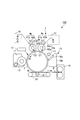
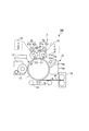
- FIG. 1 is a schematic cross-sectional view of a main part of an image forming apparatus according to an embodiment of the present invention.
- 1 is a block diagram illustrating a schematic control mode of a main part of an image forming apparatus according to an embodiment of the present invention. It is a graph for demonstrating the charging operation of the 1st charging roller in one Example of this invention.
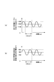
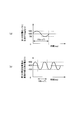
- FIG. 4 is a graph for explaining (a) a voltage applied to a first charging roller and (b) a potential of a photoconductor immediately after passing through a first charging position in an embodiment of the present invention.
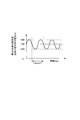
- FIG. 6 is a graph for explaining the potential of the photoconductor immediately before reaching the second charging position in the embodiment of the present invention.
- FIG. 4 is a graph for explaining (a) a voltage applied to a first charging roller and (b) a potential of a photoconductor immediately after passing through a first charging position in an embodiment of the present invention.
- FIG. 6 is a graph for explaining the potential of the photoconduct
- FIG. 6 is a graph for explaining the potential of the photoconductor immediately after passing through a second charging position in an embodiment of the present invention. It is a graph for demonstrating the electric current which flows into the 2nd charging roller in one Example of this invention. It is a schematic diagram for demonstrating the relationship between the charging polarity of the deposit
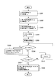
- FIG. 6 is a flowchart of an image forming operation in an embodiment of the present invention.
- FIG. 6 is a timing chart of an image forming operation in an embodiment of the present invention. It is a typical sectional view of the important section of the image forming device concerning other examples of the present invention.
- FIG. 6 is a graph for explaining (a) a voltage applied to a first charging roller and (b) a potential of a photoconductor immediately after passing through a first charging position in another embodiment of the present invention. It is a flowchart figure of the image formation operation
- the first charging roller 3a is a roller-type first charging member serving as a first charging unit.
- a second charging roller 3b which is a roller-shaped second charging member as a second charging unit.
- an exposure device (laser scanner) 13 as an exposure means (image writing means).
- a developing device 11 as a developing unit.
- a transfer belt 20 as a recording material carrier (conveying means).
- a cleaning device 15 as a cleaning means.
- there is a pre-charge exposure lamp 17 which is a light static elimination means as a static elimination means.
- the first and second charging rollers 3 a and 3 b constitute the charging device 2.
- a transfer roller 16 that is a roller-shaped transfer member as transfer means is disposed on the inner peripheral surface side of the transfer belt 20.
- the transfer roller 16 is pressed against the photoconductor 1 through the transfer belt 20 to form a transfer portion N where the photoconductor 1 and the transfer belt 20 are in contact with each other.
- the image forming apparatus 100 includes a feeding mechanism (not shown) for transporting a recording material (recording medium) P such as recording paper to the transfer unit N, and the downstream side of the transfer unit N in the transport direction of the recording material P.
- a fixing device 18 is provided as fixing means disposed in the area.
- the surface of the photoreceptor 1 is charged to a predetermined potential having a predetermined polarity (negative polarity in this embodiment) by the first charging roller 3a and the second charging roller 3b.
- the charging voltage (charging bias) applied to the first and second charging rollers 3a and 3b at this time will be described in detail later.
- the surface of the charged photoreceptor 1 is exposed according to image information by an exposure device 13 constituting a toner image forming unit. As a result, an electrostatic latent image (electrostatic image) is formed on the photoreceptor 1.
- the electrostatic latent image formed on the photosensitive member 1 is developed (visualized) by supplying toner as a developer by a developing device 11 constituting a toner image forming unit.
- the developing device 11 has a developing sleeve 12 as a developer carrying member, and the toner carried on the developing sleeve 12 and conveyed to a portion (developing portion) facing the photosensitive member 1 is electrostatically charged on the photosensitive member 1. It is transferred onto the photoreceptor 1 in accordance with the latent image.
- a predetermined developing voltage (developing bias) is applied to the developing sleeve 12.
- a toner image is formed by a combination of image exposure and reversal development.
- the rotation direction of the first and second charging rollers 3a and 3b is limited to the direction in which the photosensitive member 1 and the first and second charging rollers 3a and 3b face each other in the forward direction. It is not a thing.
- the first and second charging rollers 3a and 3b are not in contact with the photosensitive member 1, and the opposite portions of the photosensitive member 1 and the first and second charging rollers 3a and 3b are opposite to each other. You may rotate in the direction of movement.
- the first and second cleaning rollers 4a and 4b remove deposits such as toner and external additives attached to the surfaces of the first and second charging rollers 3a and 3b, respectively.
- Part of the adhering matter such as toner and external additives removed from the surfaces of the first and second charging rollers 3a and 3b by the first and second cleaning rollers 4a and 4b is removed by the first and second cleaning. It is supplemented by physically adhering to the foamed portions of the rollers 4a and 4b.
- Other deposits are temporarily swept from the contact portions (nip portions) with the first and second charging rollers 3a and 3b after contacting the foamed sponges of the first and second cleaning rollers 4a and 4b.
- the present invention can be implemented even if the first and second cleaning rollers 4a and 4b are not arranged. However, when the first and second cleaning rollers 4a and 4b and the first and second charging rollers 3a and 3b are brought into contact with each other and rotated, the surfaces of the first and second charging rollers 3a and 3b are attached. The effect of scattering the kimono and the effect of reducing the adhesion of the deposit can be obtained.
- the behavior of the deposit that has been recharged and returned to the photoreceptor 1 will be further described.
- the negatively charged deposit returned to the photoreceptor 1 is divided into a non-image portion and an image portion when the developing device 11 forms a toner image.
- Deposits on the non-image area on the photoreceptor 1 are collected by the developing apparatus 11 by the action of a non-image area potential difference (non-image area contrast potential difference) acting between the developing device 11 and the photoreceptor 1.
- the deposit on the image portion on the photosensitive member 1 is combined with the toner image formed by the developing device 11 by the image portion potential difference (development contrast potential difference) acting between the developing device 11 and the photosensitive member 1 and transferred. It is conveyed to the part N and transferred to the recording material P.
- the deposit that has not been transferred to the recording material P is transported to the cleaning device 15 while being adhered to the photoreceptor 1 and cleaned.
- the adhering substance is closer to the photoreceptor 1 than the surfaces of the first and second charging rollers 3a and 3b.
- the movement is different.
- the high-pressure conditions applied to the first and second charging rollers 3a and 3b and the operation for removing deposits will be described in detail later.
- a first high-voltage power source S1 as a first power source is connected to the core 31a of the first charging roller 3a.
- the first high-voltage power supply S1 includes a DC power supply unit S1a, and is configured to be able to apply a DC voltage to the first charging roller 3a and to vary the voltage value.
- the DC voltage range that can be applied to the first charging roller 3a is -200V to -2000V.
- a second high-voltage power source S2 as a second power source is connected to the core 31b of the second charging roller 3b.
- the second high-voltage power supply S2 includes a DC power supply unit S2a and an AC power supply unit S2b, and can apply an oscillating voltage in which a DC voltage and an AC voltage are superimposed on the second charging roller 3b.
- the first and second charging rollers 3a and 3b are brought into contact with the surface of the photosensitive member 1 as a member to be charged, and a voltage (charging voltage) is applied to the first and second charging rollers 3a and 3b. Is applied.
- the photosensitive member 1 is charged by a discharge generated in a minute gap between the first and second charging rollers 3 a and 3 b and the photosensitive member 1.
- the minute gaps are wedge-shaped on the upstream side and the downstream side in the rotation direction of the photoreceptor 1 in each of the first and second charging rollers 3a and 3b (shapes viewed along the rotation axis of the photoreceptor 1). One or both of the spaces.
- the first charging position C1 where the charging process of the photosensitive member 1 is performed by the first charging roller 3a, and the second charging position C2 where the charging process of the photosensitive member 1 is performed by the second charging roller 3b. are represented at the following positions. That is, the first charging position C1 is the most downstream position of the contact portion between the first charging roller 3a and the photosensitive member 1 in the rotation direction of the photosensitive member 1, and the surface of the photosensitive member 1 immediately after passing through the first charging position C1 is the first charging position C1. It is assumed that the charging process is performed by one charging roller 3a.
- the second charging position C2 is the most upstream position of the contact portion between the second charging roller 3b and the photosensitive member 1 in the rotation direction of the photosensitive member 1, and the surface of the photosensitive member 1 reaches the first position by reaching this position. It is assumed that the charging process is performed by the second charging roller 3b. Accordingly, it is assumed that a direct current flowing between the second charging roller 3b and the photosensitive member 1, which will be described later, also flows at the second charging position C2.
- the exact position where the charging process and the current flow is not important.
- a charging process is performed between reaching the upstream minute gap and passing through the downstream minute gap. It is understood that current flows. Most simply, charging processing is performed at the center position of the contact portion between the first and second charging rollers 3a and 3b and the photosensitive member 1 in the rotation direction of the photosensitive member 1, and a current flows. Even if it is imitated, there is no problem in understanding the present invention.
- a CPU 200 as a control unit of a control unit (control circuit) 400 provided in the image forming apparatus 100 comprehensively controls the operation of the image forming apparatus 100.
- a high voltage output control unit 300 Connected to the CPU 200 are a high voltage output control unit 300, a storage unit 500 for storing charging voltage control data, a timer 600 as a time measuring unit, an output number counter 700 as a counting unit for counting the number of output images, and the like. Yes.
- the first high-voltage power source S1 and the second high-voltage power source S2 are connected to the high-voltage output control unit 300.
- the CPU 200 can perform processing based on data stored in the storage unit 500 or information from the timer 600 or the counter 700, and can instruct the high voltage output control unit 300.
- the CPU 200 controls the DC voltage output from the first high-voltage power supply S1 and the DC voltage and AC voltage output from the second high-voltage power supply S2 via the high-voltage output control unit 300.
- the high-voltage output control unit 300 performs ON / OFF of the outputs of the first high-voltage power supply S1 and the second high-voltage power supply S2, detection and control of output values, and the like according to instructions from the CPU 200.
- the charging device 2 includes the first and second charging rollers 3a and 3b, the first and second cleaning rollers 4a and 4b, the first high-voltage power supply S1, the second high-voltage power supply S2, and the like.
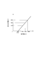
- FIG. 3 shows the relationship between the DC voltage applied to the first charging roller 3a and the potential (surface potential) of the photoreceptor 1 after charging.
- the photoreceptor 1 is charged.
- the photosensitive member 1 is charged to a potential of ⁇ 800V.
- the current flowing between the first charging roller 3a and the photosensitive member 1 is ⁇ 700 ⁇ A.
- the current flowing in the direction from the first and second charging rollers 3a and 3b to the photosensitive member 1 is defined as a “positive direction” current, and the value of the current is “ The value is positive.
- FIG. 4A shows a fluctuating voltage applied to the first charging roller 3a.
- FIG. 4B shows the potential of the photosensitive member 1 immediately after passing through the first charging position C1 (after being charged by the first charging roller 3a).
- the fluctuating voltage applied to the first charging roller 3a is a function of time.
- the fluctuation voltage applied to the first charging roller 3a at the time of image formation is fluctuated in a range of ⁇ 100V with -1200V being the center.
- the waveform of this voltage is a sine wave with a period (T) of 130 ms.
- the first charging roller 3a When the voltage as described above is applied to the first charging roller 3a, the surface of the photoreceptor 1 immediately after passing through the first charging position C1 has a potential as shown in FIG. 4B. Will be formed. That is, as shown in FIG. 4B, the first charging roller 3a causes the surface of the photosensitive member 1 to have a median value of ⁇ 800V, a fluctuation range of ⁇ 100V, and a maximum value on the charging polarity side of the photosensitive member 1. Is -900 V, the minimum value is -700 V, and a potential (fluctuation potential) having a period (T) of 130 ms is formed. As described above, the first charging roller 3 a forms a charging potential that fluctuates in the circumferential direction of the photosensitive member 1.
- FIG. 5 shows the potential of the photosensitive member 1 immediately before reaching the second charging position C2 (before charging with the second charging roller 3b).
- the dark decay of the charging potential of the photosensitive member 1 is about 100 V between the first charging position C1 and the second charging position C2.
- the surface of the photoconductor 1 immediately before reaching the second charging position C2 has a median value of ⁇ 700 V, a fluctuation range of ⁇ 100 V, a maximum value on the charge polarity side of the photoconductor 1 of ⁇ 800 V, and a minimum value of A potential (fluctuation potential) of ⁇ 600 V is formed.
- the change (fluctuation potential) of the potential of the photosensitive member 1 formed by the first charging roller 3a is set in consideration of the following two conditions. It is preferable.
- the direction of the current flowing in the second charging roller 3b (positive direction) within the contact time between the second charging roller 3b and the photoreceptor 1 is determined. (Or negative direction) may be set so as not to switch.
- “X” and “Y” may be set longer than the contact time between the second charging roller 3 b and the photoreceptor 1. Accordingly, when the contact width between the second charging roller 3b and the photosensitive member 1 in the rotation direction of the photosensitive member 1 is W (mm) and the peripheral speed of the photosensitive member 1 is PS (mm / s), the following relational expression It is preferable to set so as to satisfy.
- the reason why the “sum of X and Y” and the rotation period of the second charging roller 3b have a non-integer multiple relationship is the direction of the current flowing through the second charging roller 3b (positive direction or negative direction). This is because the part where the current is switched, that is, the part where no current flows, and the rotation period of the second charging roller 3b are shifted.
- the image forming apparatus 100 can use a plurality of types of recording materials P, a photoconductor on which a toner image corresponding to one recording material P of the minimum size used in the image forming apparatus 100 is formed.
- the sum of X and Y may be set shorter than the time during which the upper region passes through the second charging roller 3b.
- a sine wave is used as the shape of the voltage applied to the first charging roller 3a, but a voltage such as a triangular wave may be used.
- the second charging roller 3b charges the photosensitive member 1 by applying an oscillating voltage in which a DC voltage and an AC voltage are superimposed.
- FIG. 6 shows the potential of the photosensitive member 1 immediately before reaching the second charging position C2, and the potential of the photosensitive member 1 immediately after passing through the second charging position (after being charged by the second charging roller 3b). Shows the relationship.
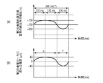
- FIG. 7A shows the potential of the photosensitive member 1 immediately before reaching the second charging position C2.
- FIG. 7B shows the current flowing through the second charging roller 3b.
- FIG. 8 shows the relationship between the direction of the current flowing through the second charging roller 3b and the charging polarity of the adhering matter such as toner or external additive attached to the surface of the second charging roller 3b.
- FIG. 8A shows a case where the current flowing between the second charging roller 3b and the photoreceptor 1 is in the positive direction. That is, FIG. 8A shows the period X in FIG. 7B.
- FIG. 8B shows a case where the current flowing between the second charging roller 3b and the photoreceptor 1 is in the negative direction. That is, FIG. 8B shows the period Y in FIG.
- a current flows from the second charging roller 3b side to the photosensitive member 1 side. That is, since the second charging roller 3b side is relatively high in the positive polarity side between the second charging roller 3b and the photosensitive member 1, a current flows from the second charging roller 3b side to the photosensitive member 1 side. Flows. As a result, the positively charged deposit on the photoreceptor 1 passes through the second charging position C2 without adhering to the second charging roller 3b. On the other hand, the negatively charged deposit on the photoreceptor 1 is collected by the second charging roller 3b.
- a current flows from the photosensitive member 1 side to the second charging roller 3b side. That is, since the photosensitive member 1 side has a relatively high potential on the positive polarity side between the second charging roller 3b and the photosensitive member 1, a current flows from the photosensitive member 1 side to the second charging roller 3b side. As a result, the negatively charged deposit on the second charging roller 3 b is returned to the photoreceptor 1. On the other hand, the positively charged deposit on the photoreceptor 1 adheres to the second charging roller 3b.
- the operation shown in FIGS. 8A and 8B is repeated at a predetermined period (T), so that the toner or external additive charged to the second charging roller 3b is positively or negatively charged. Accumulation of deposits can be reduced. Further, since the charged polarity of the deposit on the second charging roller 3b is not excessively biased to the positive polarity or the negative polarity, long-term continuous image formation is possible without providing a special cleaning mode in which image formation cannot be performed. Is possible. As a result, the downtime of the image forming apparatus 100 (the time during which no image can be output due to the cleaning operation or the adjustment operation) is reduced, and the productivity can be improved.
- T predetermined period
- the deposits moved to the photoreceptor 1 do not hinder image formation.
- most of the deposits moved to the photosensitive member 1 are subsequently collected by the developing device 11, transferred to the recording material P at the transfer portion N, or passed through the transfer portion N. Later, it is removed from the photoreceptor 1 by the cleaning device 15 and collected.
- the first and second cleaning rollers 4a and 4b are brought into contact with the first and second charging rollers 3a and 3b, respectively, so that the first and second cleaning rollers 4a and 4b operate as described above.
- the charging rollers 3a and 3b have a function of scattering the deposits on the surface and a function of reducing the adhesion force.
- a predetermined charging potential (PreVD) is formed on the photosensitive member by the first charging roller on the upstream side, and a charging process is performed by discharging by applying a superimposed voltage of an AC voltage and a DC voltage to the second charging roller on the downstream side.
- Vdc DC voltage potential
- the positive and negative charged particles on the second charging roller can be uniformly removed. That is, the cycle of PreVD formed on the photosensitive member by the first charging roller is shifted from the rotation cycle of the second charging roller so that PreVD having the same potential does not come to the same part of the second charging roller every time.
- the rotation period of the second charging roller is Ts
- the discharge start voltage when a DC voltage is applied to the charging roller is Vth.
- the maximum value on the charging polarity side of the photoconductor, VHI, and the minimum value on the charging polarity side of the photoconductor, of the charging potential of the photoconductor that reaches the second charging roller is VLO.
- the potential of the DC voltage applied to the second charging roller is Vdc.
- the image forming apparatus 100 includes the rotatable photoreceptor 1, the first charging roller 3 a in contact with or close to the photoreceptor 1, and the first charging roller 3 a in the rotation direction of the photoreceptor 1. And a second charging roller 3b in contact with or close to the photoconductor on the downstream side.
- the image forming apparatus 100 also includes a first power supply S1 that applies a fluctuating voltage whose voltage value fluctuates to the first charging roller 3a, and a voltage obtained by superimposing a DC voltage and an AC voltage on the second charging roller 3b.
- a second power source S2 Further, the image forming apparatus 100 includes a control unit 200 that varies the varying voltage applied from the first power source S1 to the first charging roller 3a during image formation.
- the control means 200 varies the varying voltage applied to the first charging roller 3a as follows. That is, the potential of the photoconductor 1 that is charged by the first charging roller 3a and reaches the position where the photoconductor 1 is charged by the second charging roller 3b, and the DC voltage applied to the second charging roller 3b. The magnitude relationship with the potential is switched alternately.
- the control unit 200 applies a fluctuating voltage applied from the first power source S1 to the first charging roller 3a during image formation to a voltage larger than the discharge start voltage on the charging polarity side of the photoconductor 1. Vary in the range of values. In one embodiment, the median value of the fluctuation voltage applied to the first charging roller 3a and the potential of the DC voltage applied to the second charging roller 3b during image formation are substantially equal.
- a cost reduction is realized by using a DC voltage source capable of changing the voltage value as the first power supply S1 for applying the fluctuation voltage to the first charging roller 3a.
- the upper limit of the fluctuation amount of the fluctuation voltage when the DC power supply that outputs a voltage of one side polarity is used as the first power supply S1 as in the present embodiment, the lower limit value of the voltage value that can charge the photosensitive member.
- the discharge start voltage Vth is substantially the lower limit value of the fluctuation voltage.
- the median value of the fluctuation voltage and the lower limit value of the fluctuation voltage described above are used. It is preferable to set the voltage having the same potential difference as Vth as the upper limit of the maximum value.
- which is the amount of change in the charged potential of the photoconductor reaching the second charging roller, satisfies the relationship
- the current that flows when the photosensitive member is charged with the first charging roller 3a so as to have a median value of the fluctuation potential is preferable that 10% or more of the current is the potential of the photosensitive member flowing between the second charging roller 3b and the photosensitive member.
- the photosensitive member is charged to -800V by the first charging roller 3a.
- the resistance values of the first charging roller 3a and the second charging roller 3b are the same, at least 70 ⁇ A or more.
- variable voltage is set so that the potential difference between the potential of the photosensitive member and the DC voltage value of the second charging roller 3b is 80V or more.
- Set the fluctuation amount of It is preferable to set.
- the CPU 200 controls the image forming apparatus 100 according to the following procedure in response to the input of the image forming signal.
- the CPU 200 rotates the photosensitive member 1 and exposes the photosensitive member 1 with the pre-charging exposure lamp 17 (S101).
- the CPU 200 applies a fluctuation voltage (DC voltage) having a predetermined period (T) from the first high-voltage power supply S1 to the first charging roller 3a at a timing when the photoreceptor 1 has reached the steady rotation.
- the photoconductor 1 is charged by the output (S102).
- the CPU 200 controls the exposure device 13 to start image formation (S104). Thereafter, the image forming operation is continued until the CPU 200 issues an image formation end command (S105).
- the first charging roller 3a is used to form a variable potential of the photoreceptor 1 having a predetermined period (T). Further, in the second charging roller 3b, currents in both positive and negative directions are alternately alternated at a predetermined cycle (T) by the potential of the photoreceptor 1 before charging and the potential of the DC voltage applied to the second charging roller 3b. Flowing.
- the second high voltage power source S2 outputs an oscillation voltage in which the DC voltage and the AC voltage are superimposed on the second charging roller 3b, and is output by the second charging roller 3b.
- the photosensitive member 1 is charged.
- image formation is started from time t3 (about 900 ms).
- the high-voltage outputs of the first and second high-voltage power sources S1 and S2 the pre-charge exposure lamp 17 are turned on, and the rotational driving of the photosensitive member 1 is sequentially stopped, and a series of image forming operations is performed. Ends.
- accumulation of deposits such as toner on the charging member can be suppressed without providing a special period during which image formation cannot be performed and cleaning of the charging member is performed. Can be improved.
- the charging voltage applied to the first charging roller 3a an oscillating voltage obtained by superimposing an alternating voltage having a shorter cycle than the varying voltage on the varying voltage similar to that in the first embodiment is applied.
- the stability of the potential of the photoreceptor 1 formed by the first charging roller 3a is improved.
- FIG. 11 is a schematic cross-sectional view showing a configuration of a main part of the image forming apparatus 100 of the present embodiment.
- FIG. 12 is a block diagram showing a control mode of the main part of the image forming apparatus 100 of this embodiment. *
- a first high-voltage power source S3 as a first power source is connected to the core 31a of the first charging roller 3a.
- the first high-voltage power supply S3 includes a variable voltage power supply unit S3a that supplies a variable voltage and an AC power supply unit S3b that supplies an AC voltage, and an oscillation voltage in which the variable voltage and the AC voltage are superimposed on the first charging roller 3a. Can be applied.
- the first high-voltage power source S3 is connected to the high-voltage output control unit 300.
- the first high-voltage power source S3 has a common configuration with the second high-voltage power source S2.
- FIG. 13A shows the change over time of the varying voltage applied to the first charging roller 3a.
- FIG. 13B shows the change over time of the potential of the photoreceptor 1 immediately after passing through the first charging position C1.
- a fluctuation voltage having a median value of ⁇ 800V and a fluctuation width of ⁇ 100V is applied to the first charging roller 3a.
- the waveform of this voltage is a sine wave with a period (T) of 130 ms.
- an alternating voltage having a peak-to-peak voltage Vpp of 1200 V and a frequency of 5.86 KHz is applied to the first charging roller 3a so as to be superimposed on the above fluctuation voltage. That is, a vibration voltage having a median value of ⁇ 800 V is applied to the first charging roller 3a.
- a potential as shown in FIG. 13B is formed on the surface of the photoreceptor 1 immediately after passing through the first charging position C1. That is, a potential (fluctuation potential) having a median value of ⁇ 800 V, a fluctuation range of ⁇ 100 V, a maximum value on the charging polarity side of the photoreceptor 1 of ⁇ 900 V, a minimum value of ⁇ 700 V, and a period (T) of 130 ms is formed. .
- the first charging roller 3 a forms a charging potential that fluctuates in the circumferential direction of the photosensitive member 1.
- steps S201 to S206 in the flowchart in FIG. 14 is the same as the processing in steps S101 to S106 in the flowchart in FIG. 9 described in the first embodiment. However, the difference is that in S202, an alternating voltage is superimposed on the variable voltage and the vibration voltage is output from the second high-voltage power source S3 to the first charging roller 3a.
- the central value of the fluctuation potential of the photosensitive member 1 formed by the first charging roller 3a is set to the positive side or the negative side with respect to the potential of the DC voltage applied to the second charging roller 3b. Set the value shifted in one direction. As a result, the removal efficiency of deposits such as toner and external additives on the photoreceptor 1 that is easily charged to one of positive polarity and negative polarity is improved.
- FIG. 15A shows a change with time of the potential of the photoreceptor 1 immediately before reaching the second charging position C2.
- FIG. 15B shows a change over time of the current flowing through the second charging roller 3b.
- the median of the potential of the photosensitive member 1 immediately before reaching the second charging position C2 is ⁇ 700V
- the maximum value on the charging polarity side of the photosensitive member 1 is ⁇ 800V
- the minimum value is -550V. That is, in this embodiment, the amplitude of the potential of the photosensitive member 1 in the period corresponding to Y is made larger than the period corresponding to X.
- the setting of the voltage applied to the second charging roller 3b is the same as that in the first embodiment, and the DC voltage applied to the second charging roller 3b is -700V.
- the current flowing through the second charging roller 3b is larger in the negative direction than in the positive direction.
- the maximum value in the positive direction of the current flowing through the second charging roller 3b during the period X is 87.5 ⁇ A
- the negative value and the positive value of the difference between the potential of the photosensitive member 1 that alternately switches during image formation and the potential of the DC voltage applied to the second charging member 3b are as follows: The maximum absolute value of the difference is different.
- the current flowing through the second charging roller 3b is larger in the negative direction than in the positive direction. That is, it becomes easy to move the negatively charged deposit to the photosensitive member 1 side. Therefore, the deposits such as toner and external additives on the photoreceptor 1 that pass through the second charging position C2 can be biased toward the negative polarity side. Further, since a positive current also flows through the second charging roller 3b due to the fluctuation potential of the photosensitive member 1, it is possible to suppress the accumulation of positively charged deposits on the second charging roller 3b. And stable image formation is possible.
- the current flowing through the second charging roller 3b is larger in the negative direction than in the positive direction.
- the charging polarity of the toner, the external additive, and the photosensitive member 1 it is possible to appropriately change the positive direction or the negative direction, or the ratio of the positive and negative currents.
- the time X when the difference between the potential of the photoreceptor 1 immediately before reaching the second charging position C2 and the potential of the DC voltage applied to the second charging roller 3b is a negative value.
- the time Y, which is the positive value, is set to a different value (the ratio of X and Y is shifted from 1: 1). This improves the removal efficiency of deposits such as toner and external additives on the photosensitive member 1 that are easily charged to one of the positive polarity and the negative polarity.
- the fluctuation potential of the photosensitive member 1 formed by the first charging roller 3a is set so that the positive current flowing through the second charging roller 3b is longer than the negative current.
- the potential of the photoconductor 1 immediately before reaching the second charging position C2 has a median value of ⁇ 700 V, a fluctuation range of ⁇ 50 V, and a maximum value on the charging polarity side of the photoconductor 1. Is a fluctuation potential of ⁇ 750V, and the minimum value is ⁇ 650V.
- the setting of the voltage applied to the second charging roller 3b is the same as that in the first embodiment, and the DC voltage applied to the second charging roller 3b is -700V.
- the ratio of X and Y was set to 2: 1 with the time Y that is the value of Y being different.
- X is 260 ms and Y is 130 ms.
- the time ratio between the period X in which the positive current flows in the second charging roller 3b and the period Y in which the negative current flows is biased to 2: 1.
- the maximum value of the positive current flowing through the second charging roller 3b during the period X is 43 ⁇ A
- the maximum value of the negative current flowing through the second charging roller 3b during the period Y is ⁇ 43 ⁇ A.
- the time during which the difference between the potential of the photosensitive member 1 alternately switched during image formation and the potential of the DC voltage applied to the second charging member 3b takes a negative value is X (s. ), Where the positive time is Y (s), the ratio of X and Y is biased to X or Y.
- the time during which the positive current flows through the second charging roller 3b is set longer than the time during which the negative current flows.
- the time in which the positive direction or the negative direction flows is increased, or the ratio of the time in which the current in the positive direction and the negative direction flows is appropriately changed. can do.
- the time ratio between the times X and Y in which the current in the positive direction and the negative direction flows may be changed for each predetermined number of output sheets using the output number counter 700 provided in the image forming apparatus 100.
- the time ratio of X and Y is controlled to 2: 1 for a period of up to 1000 sheets of A4 horizontal size, and then the time ratio of x and Y is switched to 3: 1.
- the time ratio of x and Y is switched to 3: 1.
- the setting of the voltage applied to the second charging roller 3b is the same as that in the first embodiment, and the DC voltage applied to the second charging roller 3b is -700V.
- the maximum value of the positive current flowing during the period X is set to be larger than that of the fourth embodiment. Increased to 86 ⁇ A. The maximum value of the current flowing during the period Y remains the same as ⁇ 43 ⁇ A in the fourth embodiment.
- the fluctuation voltage applied to the first charging roller 3a has a median value of ⁇ 1200V and fluctuation ranges of two stages of ⁇ 75V and ⁇ 150V. Then, using this output number counter 700, the fluctuation range is switched every 1000 image output sheets.
- the CPU 200 controls the image forming apparatus 100 according to the following procedure in response to the input of the image forming signal.
- the CPU 200 applies a fluctuation voltage (DC voltage) having a predetermined period (T) from the first high-voltage power supply S1 to the first charging roller 3a at a timing when the photoreceptor 1 has reached the steady rotation.
- the photosensitive member 1 is charged by outputting (S302).
- the fluctuation range of the fluctuation voltage is set to ⁇ 75V.
- the CPU 200 resets the count number P of the output number counter 700 used for switching the dynamic potential to 0 (S304).
- the CPU 200 determines the end of the job (S307).
- the CPU 200 switches the fluctuation range of the fluctuation voltage applied to the first charging roller 3a to ⁇ 150 V and resets the count number P of the counter 700 to 0 (S309). ). Subsequently, the processing proceeds to S307, and the CPU 200 determines the end of the job.
- the control unit 200 determines the maximum absolute value of the difference between the potential of the photosensitive member 1 that reaches the second charging position C2 and the potential of the DC voltage applied to the second charging roller 3b. Switch periodically. Thereby, the removal effect of the deposits on the second charging roller 3b is improved.
Landscapes
- Physics & Mathematics (AREA)
- General Physics & Mathematics (AREA)
- Engineering & Computer Science (AREA)
- Plasma & Fusion (AREA)
- Electrostatic Charge, Transfer And Separation In Electrography (AREA)
Description
本発明は、電子写真方式を用いた複写機、プリンターなどの画像形成装置に関するものである。
従来、電子写真方式の画像形成装置では、帯電手段で電子写真感光体(感光体)を帯電させ、露光手段を用いて露光することで感光体上に静電像を形成し、この静電像を現像手段により現像して感光体上にトナー像を形成する。
帯電手段としては、コロナ帯電方式よりも放電時のオゾンの発生が少ないため、被帯電体に接触又は近接させた帯電部材を用いる接触帯電方式が広く利用されている。中でも、ローラ型の帯電部材である帯電ローラを用いる帯電ローラ方式が広く利用されている。帯電ローラ方式では、一般に、ローラ状の帯電部材である帯電ローラを被帯電体である感光体の表面に接触させて、この帯電ローラに電圧(帯電電圧)を印加することで、帯電ローラと感光体との間の微小な空隙で発生する放電により感光体を帯電させる。
尚、上記帯電ローラなどの帯電部材は、被帯電体である感光体の表面に必ずしも接触している必要はない。帯電ローラと感光体との間に、ギャップ間電圧と補正パッシェンカーブで決まる放電可能領域さえ確実に保証されれば、例えば数10μmの空隙(間隙)を有して非接触に近接配置されていてもよい。ここでは、帯電ローラを被帯電体に接触又は近接させて、微小な空隙で発生する放電により被帯電体を帯電させる方式を接触又は近接帯電方式又は単に接触帯電方式と呼ぶ。
電子写真方式の画像形成装置における帯電方式として接触帯電方式を用いる場合、感光体に付着した転写残トナーや外添剤などの異物が帯電部材に付着し、帯電ムラに起因する画像不良が発生することがある。
そこで、複数の帯電ローラを用いることによって、感光体の回転方向上流側に配置されている帯電ローラに異物が付着することによって発生した帯電ムラを下流側に配置されている帯電ローラでも帯電を行うことによって補完して帯電均一性を保つことができる期間を延ばす構成が知られているが、この場合においても累積画像形成枚数が多くなれば異物が感光体の回転方向下流の帯電ローラにも付着して帯電ムラに起因する画像不良が発生するという問題は依然存在している。
そこで、特許文献1では、複数の帯電ローラを有する場合において、非画像形成時に、感光体の回転方向における上流側の帯電ローラで形成した感光体の帯電電位と下流側の帯電ローラに印加される直流電圧との電位差により、下流側の帯電ローラに付着した付着物を除去するクリーニングモードを有することが記載されている。
しかしながら、特許文献1に記載されているような、非画像形成時に帯電ローラの清掃を行う方法は、連続画像形成動作中にダウンタイムを設けて、清掃動作を実施する必要があり、画像形成装置の生産性を低下させる問題がある。
従って、本発明は、複数の帯電ローラを備えた画像形成装置において、画像形成装置の生産性を低下させることなく、帯電ローラへの外添剤などの付着物の蓄積を抑制することを目的とする。
本発明は、
回転可能な感光体;
前記感光体を帯電する第1の帯電ローラと、前記感光体の回転方向において前記第1の帯電ローラよりも下流側で前記感光体を帯電する第2の帯電ローラと、前記感光体の回転方向において前記第2の帯電ローラよりも下流側に配置され、前記第1の帯電ローラおよび前記第2の帯電ローラによって帯電された感光体の表面に潜像を形成し、潜像をトナーで現像してトナー像を形成するトナー像形成部と、前記第1の帯電ローラに電圧値を変動させた変動電圧を印加する第1の電源と、前記第2の帯電ローラに直流電圧と交流電圧とを重畳させた電圧を印加する第2の電源と、トナー像を形成するために前記第1の帯電ローラおよび前記第2の帯電ローラで前記感光体を帯電させるとき、前記第1の帯電ローラに帯電されて前記第2の帯電ローラが帯電する位置に到達する前記感光体の電位と、前記第2の帯電ローラに印加される直流電圧値との大小関係が、交互に切り替わるように前記第1の電源から前記第1の帯電ローラに印加する前記変動電圧を変動させる制御手段とを備え、トナー像を形成するために前記第1の帯電ローラおよび前記第2の帯電ローラで前記感光体を帯電させるとき、前記第1の帯電ローラに帯電されて前記第2の帯電ローラが帯電する位置に到達する前記感光体表面の電位が前記第2の帯電ローラに印加される直流電圧よりも小さい値となる時間をX(s)、大きい値となる時間をY(s)、前記感光体の周速度をPS(mm/s)、前記感光体の回転方向における前記第2の帯電ローラと前記感光体との接触幅をW(mm)としたとき、
X>(W/PS)、 Y>(W/PS)
の関係を満たし、
XとYの和は前記第2の帯電ローラに印加される交流電圧の周期よりも大きいことを特徴とする画像形成装置である。
回転可能な感光体;
前記感光体を帯電する第1の帯電ローラと、前記感光体の回転方向において前記第1の帯電ローラよりも下流側で前記感光体を帯電する第2の帯電ローラと、前記感光体の回転方向において前記第2の帯電ローラよりも下流側に配置され、前記第1の帯電ローラおよび前記第2の帯電ローラによって帯電された感光体の表面に潜像を形成し、潜像をトナーで現像してトナー像を形成するトナー像形成部と、前記第1の帯電ローラに電圧値を変動させた変動電圧を印加する第1の電源と、前記第2の帯電ローラに直流電圧と交流電圧とを重畳させた電圧を印加する第2の電源と、トナー像を形成するために前記第1の帯電ローラおよび前記第2の帯電ローラで前記感光体を帯電させるとき、前記第1の帯電ローラに帯電されて前記第2の帯電ローラが帯電する位置に到達する前記感光体の電位と、前記第2の帯電ローラに印加される直流電圧値との大小関係が、交互に切り替わるように前記第1の電源から前記第1の帯電ローラに印加する前記変動電圧を変動させる制御手段とを備え、トナー像を形成するために前記第1の帯電ローラおよび前記第2の帯電ローラで前記感光体を帯電させるとき、前記第1の帯電ローラに帯電されて前記第2の帯電ローラが帯電する位置に到達する前記感光体表面の電位が前記第2の帯電ローラに印加される直流電圧よりも小さい値となる時間をX(s)、大きい値となる時間をY(s)、前記感光体の周速度をPS(mm/s)、前記感光体の回転方向における前記第2の帯電ローラと前記感光体との接触幅をW(mm)としたとき、
X>(W/PS)、 Y>(W/PS)
の関係を満たし、
XとYの和は前記第2の帯電ローラに印加される交流電圧の周期よりも大きいことを特徴とする画像形成装置である。
本発明によれば、画像形成を行えない特別な期間を設けて帯電部材の清掃を行わなくても、帯電部材へのトナーなどの付着物の蓄積を抑制することができる。
以下、本発明に係る画像形成装置を図面に則して更に詳しく説明する。
1.画像形成装置の全体的な構成及び動作
図1は、本発明の一実施例に係る画像形成装置100の要部の構成を示す模式的な断面図である。又、図2は、本実施例の画像形成装置100の要部の制御態様を示すブロック図である。本実施例では、画像形成装置100は、電子写真方式を用いたプリンターである。
図1は、本発明の一実施例に係る画像形成装置100の要部の構成を示す模式的な断面図である。又、図2は、本実施例の画像形成装置100の要部の制御態様を示すブロック図である。本実施例では、画像形成装置100は、電子写真方式を用いたプリンターである。
画像形成装置100は、像担持体としての円筒形状の電子写真感光体(感光体)1を有する。感光体1は、回転可能に支持されており、駆動手段としての駆動モータ(図示せず)により図中矢印R1方向(反時計回り)に回転駆動される。
感光体1の周囲には、その回転方向に沿って上流側から、次の各手段が配置されている。先ず、第1の帯電手段としてのローラ形の第1の帯電部材である第1の帯電ローラ3aである。次に、第2の帯電手段としてのローラ形の第2の帯電部材である第2の帯電ローラ3bである。次に、露光手段(画像書き込み手段)としての露光装置(レーザースキャナー)13である。次に、現像手段としての現像装置11である。次に、記録材担持体(搬送手段)としての転写ベルト20である。次に、クリーニング手段としてのクリーニング装置15である。次に、除電手段としての光除電手段である帯電前露光ランプ17である。第1、第2の帯電ローラ3a、3bは、帯電装置2を構成する。
又、転写ベルト20の内周面側には、転写手段としてのローラ形の転写部材である転写ローラ16が配置されている。転写ローラ16は、転写ベルト20を介して感光体1に押圧され、感光体1と転写ベルト20とが接触する転写部Nを形成する。
その他、画像形成装置100には、記録用紙などの記録材(記録媒体)Pを転写部Nへと搬送する給送機構(図示せず)、記録材Pの搬送方向において転写部Nの下流側に配置された定着手段としての定着装置18が設けられている。
画像形成時には、感光体1の表面が第1の帯電ローラ3a及び第2の帯電ローラ3bによって所定の極性(本実施例では負極性)の所定の電位に帯電させられる。このときに第1、第2の帯電ローラ3a、3bに印加される帯電電圧(帯電バイアス)については後述して詳しく説明する。
帯電した感光体1の表面は、トナー像形成部を構成する露光装置13によって画像情報に応じて露光される。これにより、感光体1上に静電潜像(静電像)が形成される。
感光体1上に形成された静電潜像は、トナー像形成部を構成する現像装置11によって現像剤としてのトナーが供給されて現像(顕像化)される。現像装置11は、現像剤担持体としての現像スリーブ12を有し、現像スリーブ12に担持されて感光体1との対向部(現像部)に搬送されたトナーが、感光体1上の静電潜像に応じて感光体1上に転移させられる。現像動作時に、現像スリーブ12には、所定の現像電圧(現像バイアス)が印加される。本実施例では、イメージ露光と反転現像との組み合わせにより、トナー像が形成される。即ち、帯電処理された後に露光されることで電位の絶対値が低下した感光体1上の露光部に、感光体1の帯電極性と同極性(本実施例では負極性)に帯電したトナーを付着させる。本実施例では、感光体1上の静電潜像を現像するトナーの意図された帯電極性(正規の帯電極性)は負極性である。
感光体1上に形成されたトナー像は、転写部Nに搬送される。このタイミングに合わせて転写ベルト20によって転写部Nまで記録材Pが搬送されてくる。そして、転写ローラ16の作用によって、感光体1上から転写ベルト20に担持された記録材P上にトナー像が転写される。このとき、転写ローラ16には、トナーの正規の帯電極性とは逆極性(本実施例では正極性)の直流電圧である転写電圧(転写バイアス)が印加される。
トナー像が転写された記録材Pは、転写ベルト20から分離されて定着装置18まで搬送される。定着装置18は、熱と圧力によってトナー像を記録材Pに定着させる。その後、記録材Pは、画像形成装置100の外部に排出される。
一方、転写工程後に感光体1の表面に残留したトナー(転写残トナー)は、クリーニング装置15によって清掃される。クリーニング装置15は、クリーニング部材としてのクリーニングブレード15aによって、回転する感光体1の表面から転写残トナーを除去し、廃トナー容器15aに回収する。
又、感光体1は、帯電前露光前ランプ17によって光が照射されることで残留電荷が除去された後に、第1、第2の帯電ローラ3a、3bにより帯電処理される。
2.感光体
本実施例では、感光体1は、回転可能なドラム型の電子写真感光体、即ち、感光ドラムである。本実施例では、感光体1は、負帯電性のアモルファスシリコン感光体で、外径84mm、長さ(回転軸線方向)381mmであり、850mm/secの周速度で図中矢印R1方向(反時計回り)に回転駆動される。この感光体1は、アルミニウム製のシリンダ(導電性の基体)の表面に感光層を有する。本実施例では、感光層の膜厚は、約30μmである。尚、感光体1としては、有機感光体(OPC)などを用いてもよい。
本実施例では、感光体1は、回転可能なドラム型の電子写真感光体、即ち、感光ドラムである。本実施例では、感光体1は、負帯電性のアモルファスシリコン感光体で、外径84mm、長さ(回転軸線方向)381mmであり、850mm/secの周速度で図中矢印R1方向(反時計回り)に回転駆動される。この感光体1は、アルミニウム製のシリンダ(導電性の基体)の表面に感光層を有する。本実施例では、感光層の膜厚は、約30μmである。尚、感光体1としては、有機感光体(OPC)などを用いてもよい。
3.帯電装置
本実施例では、感光体1の周面を一様に帯電させるための帯電装置2は、帯電部材として2つのローラ形の帯電部材である第1、第2の帯電ローラ3a、3bを有する。感光体1の回転方向において、上流側に第1の帯電ローラ3a、下流側に第2の帯電ローラ3bが配置されている。第1、第2の帯電ローラ3a、3bは、それぞれ感光体1に接触している。第1、第2の帯電ローラ3a、3bは、その長手方向(回転軸線方向)の両端部において、付勢手段としての加圧バネによって感光体1の表面に押圧されている。第1、第2の帯電ローラ3a、3bは、感光体1の回転に対して従動して回転する。第1、第2の帯電ローラ3a、3bの回転軸線方向は、感光体1の回転軸線方向と略平行である。
本実施例では、感光体1の周面を一様に帯電させるための帯電装置2は、帯電部材として2つのローラ形の帯電部材である第1、第2の帯電ローラ3a、3bを有する。感光体1の回転方向において、上流側に第1の帯電ローラ3a、下流側に第2の帯電ローラ3bが配置されている。第1、第2の帯電ローラ3a、3bは、それぞれ感光体1に接触している。第1、第2の帯電ローラ3a、3bは、その長手方向(回転軸線方向)の両端部において、付勢手段としての加圧バネによって感光体1の表面に押圧されている。第1、第2の帯電ローラ3a、3bは、感光体1の回転に対して従動して回転する。第1、第2の帯電ローラ3a、3bの回転軸線方向は、感光体1の回転軸線方向と略平行である。
尚、第1、第2の帯電ローラ3a、3bの回転方向は、感光体1と第1、第2の帯電ローラ3a、3bとの対向部において両者が順方向に移動する方向に限定されるものではない。例えば、第1、第2の帯電ローラ3a、3bを感光体1に対して非接触にして、感光体1と第1、第2の帯電ローラ3a、3bとの対向部において両者が逆方向に移動する方向に回転させてもよい。
本実施例では、第1、第2の帯電ローラ3a、3bは、実質的に同一の構成を有する。第1、第2の帯電ローラ3a、3bは、それぞれ芯材としての金属製の芯金部31a、31bの表面に、半導電性の弾性ゴムで形成された弾性層32a、32bを有する。第1、第2の帯電ローラ3a、3bの外径はφ14mm、芯金31a、31bの直径はφ8mmである。又、弾性層5a、5bを形成する半導電性の弾性ゴムの体積抵抗率は104~107Ω・cmである。
又、本実施例では、帯電装置2は、第1、第2の帯電ローラ3a、3bをそれぞれ清掃する清掃部材として、第1、第2の清掃ローラ4a、4bを有する。本実施例では、第1、第2の清掃ローラ4a、4bは、実質的に同一の構成を有する。第1、第2の清掃ローラ4a、4bは、それぞれ芯材としての芯金41a、41bの上に発泡スポンジで形成された弾性層42a、42bを有する。第1、第2の清掃ローラ4a、4bは、それぞれ付勢手段としての加圧バネによって第1、第2の帯電ローラ3a、3bの表面に押圧されている。第1、第2の清掃ローラ4a、4aは、それぞれ第1、第2の帯電ローラ3a、3bの回転に対して従動して回転する。第1、第2の清掃ローラ4a、4bにより、それぞれ第1、第2の帯電ローラ3a、3bの表面に付着したトナーや外添剤などの付着物が除去される。第1、第2の清掃ローラ4a、4bによって第1、第2の帯電ローラ3a、3bの表面から除去されたトナーや外添剤などの付着物の一部は、第1、第2の清掃ローラ4a、4bの発泡部に物理的に付着して補足される。その他の付着物は、一時的に第1、第2の清掃ローラ4a、4bの発泡スポンジに接触した後、第1、第2の帯電ローラ3a、3bとの接触部(ニップ部)より掃きだされ、第1、第2の帯電ローラ3a、3bの表面側に戻される。本発明は、第1、第2の清掃ローラ4a、4bが配置されてない構成であっても実施可能である。しかし、第1、第2の清掃ローラ4a、4bと第1、第2の帯電ローラ3a、3bとを接触させて回転させることにより、第1、第2の帯電ローラ3a、3bの表面の付着物を散らす効果と、その付着物の付着力を低減する効果とが得られる。
ここで、第1、第2の帯電ローラ3a、3b上の付着物であって、第1、第2の清掃ローラ4a、4bと接触した後に第1、第2の帯電ローラ3a、3bの表面より除去された付着物が、その後除去される動作の概略について説明する。
第1、第2の帯電ローラ3a、3bの表面に再付着した付着物は、感光体1との接触部に搬送され、第1、第2の帯電ローラ3a、3bが感光体1を帯電して電位を形成する際の放電により再帯電される。この感光体1の帯電動作時に流れる電流の方向に応じて、感光体1側に戻されなかった帯電極性の付着物は、再度、第1、第2の清掃ローラ4a、4bとの接触部に戻される。又、第1、第2の帯電ローラ3a、3b上より感光体1側に移動した付着物は、現像装置11及びクリーニング15に回収される。
再帯電されて感光体1に戻された付着物の挙動について更に説明する。感光体1に戻された負極性に帯電した付着物は、現像装置11がトナー像を形成する際に、非画像部と画像部とに分かれる。感光体1上の非画像部の付着物は、現像装置11と感光体1との間に働く非画像部電位差(非画像部コントラスト電位差)の作用により、現像装置11に回収される。又、感光体1上の画像部の付着物は、現像装置11と感光体1との間に働く画像部電位差(現像コントラスト電位差)により、現像装置11により形成されるトナー像と合成され、転写部Nに搬送され、記録材Pに転写される。ここで、記録材Pに転写されなかった付着物は、感光体1に付着した状態でクリーニング装置15に搬送されてクリーニングされる。
尚、本実施例では、第1、第2の帯電ローラ3a、3bに印加される高圧条件が異なるので、第1、第2の帯電ローラ3a、3bの表面より付着物が感光体1側に移動する際の動作が異なる。第1、第2の帯電ローラ3a、3bに印加される高圧条件及び付着物の除去動作に関しては、後述して更に詳細に説明する。
又、本実施例における、第1、第2の清掃ローラ4a、4bの弾性層42a、42bを形成する発砲スポンジは、絶縁性のウレタン発泡体である。よって、第1、第2の帯電ローラ3a、3bによる感光体1の帯電動作には影響しない。
第1の帯電ローラ3aの芯金31aには、第1の電源としての第1の高圧電源S1が接続されている。第1の高圧電源S1は、直流電源部S1aを備え、第1の帯電ローラ3aに直流電圧を印加することができ、且つ電圧値を変動させることができるように構成されている。
本実施例では、第1の帯電ローラ3aに印加可能な直流電圧の範囲は、-200V~-2000Vである。
第2の帯電ローラ3bの芯金31bには、第2の電源としての第2の高圧電源S2が接続されている。第2の高圧電源S2は、直流電源部S2aと交流電源部S2bとを備え、第2の帯電ローラ3bに直流電圧と交流電圧とを重畳した振動電圧を印加することができる。
本実施例では、第2の帯電ローラ3bに印加可能な直流電圧の範囲は、-500V~-1000Vである。又、本実施例では、第2の帯電ローラ3bに印加される交流電圧は、周波数が5.86KHzであり、ピーク間電圧Vppは0V~2000Vの範囲で変更可能である。
本実施例では、第1、第2の帯電ローラ3a、3bを被帯電体である感光体1の表面に接触させて、この第1、第2の帯電ローラ3a、3bに電圧(帯電電圧)を印加する。これにより、第1、第2の帯電ローラ3a、3bと感光体1との間の微小な空隙で発生する放電により感光体1を帯電させる。上記微小な空隙は、第1、第2の帯電ローラ3a、3bのそれぞれにおける、感光体1の回転方向の上流側、下流側の楔形(感光体1の回転軸線に沿って見た形状)の空間のうち一方又は両方である。感光体1や第1、第2の帯電ローラ3a、3bの寸法、電気的抵抗などの種々の設定により、上記上流側、下流側の空隙のいずれにおいて主に感光体1の帯電処理が行われるかは変わるが、本発明では斯かる設定は任意である。
以下の説明では、便宜上、第1の帯電ローラ3aにより感光体1の帯電処理を行う第1の帯電位置C1、第2の帯電ローラ3bによって感光体1の帯電処理を行う第2の帯電位置C2は、それぞれ次の位置で代表するものとする。即ち、第1の帯電位置C1は、感光体1の回転方向において第1の帯電ローラ3aと感光体1との接触部の最下流位置とし、ここを通過した直後の感光体1の表面が第1の帯電ローラ3aによって帯電処理されているものとする。又、第2の帯電位置C2は、感光体1の回転方向において第2の帯電ローラ3bと感光体1との接触部の最上流位置とし、ここに到達することで感光体1の表面は第2の帯電ローラ3bによって帯電処理されるものとする。従って、後述する第2の帯電ローラ3bと感光体1との間で流れる直流電流も、この第2の帯電位置C2で流れるものと擬制される。
但し、本発明において、帯電処理や電流が流れる厳密な位置は重要ではない。第1、第2の帯電ローラ3a、3bのそれぞれについて、おおよそ上記上流側の微小な間隙に到達してから上記下流側の微小な間隙を通過するまでの間に、帯電処理が行われ、又電流が流れるものと理解される。最も簡易には、感光体1の回転方向における第1、第2の帯電ローラ3a、3bのそれぞれと感光体1との接触部の中央位置で、帯電処理が行われ、又電流が流れるものと擬制しても、本発明の理解においては問題ない。
4.制御態様
図2を参照して、本実施例では、画像形成装置100に設けられたコントロール部(制御回路)400の制御手段としてのCPU200が、画像形成装置100の動作を統括的に制御する。
図2を参照して、本実施例では、画像形成装置100に設けられたコントロール部(制御回路)400の制御手段としてのCPU200が、画像形成装置100の動作を統括的に制御する。
CPU200には、高圧出力制御部300、帯電電圧の制御データなどを格納する記憶部500、時間計測手段としてのタイマー600、画像出力枚数を計数する計数手段としての出力枚数カウンター700などが接続されている。第1の高圧電源S1、第2の高圧電源S2は、高圧出力制御部300に接続されている。
CPU200は、記憶部500に記憶されたデータ、或いはタイマー600やカウンター700からの情報に基づいて処理を行い、高圧出力制御部300に命令することができる。CPU200は、高圧出力制御部300を介して、第1の高圧電源S1が出力する直流電圧、並びに、第2の高圧電源S2が出力する直流電圧及び交流電圧を制御する。高圧出力制御部300は、CPU200の指示により、第1の高圧電源S1、第2の高圧電源S2の出力のON/OFF、出力値の検知及び制御などを実施する。
第1、第2の帯電ローラ3a、3b、第1、第2の清掃ローラ4a、4b、第1の高圧電源S1、第2の高圧電源S2などによって帯電装置2が構成される。
5.帯電動作
5-1.第1の帯電ローラの帯電動作
先ず、第1の帯電ローラ3aによる帯電動作について説明する。第1の帯電ローラ3aは、電圧値が変動する変動電圧が印加されることで、感光体1を帯電させる。
5-1.第1の帯電ローラの帯電動作
先ず、第1の帯電ローラ3aによる帯電動作について説明する。第1の帯電ローラ3aは、電圧値が変動する変動電圧が印加されることで、感光体1を帯電させる。
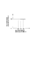
図3は、第1の帯電ローラ3aに印加する直流電圧と帯電後の感光体1の電位(表面電位)との関係を示す。図3に示すように、第1の高圧電源S1から第1の帯電ローラ3aに印加される直流電圧が、放電開始電圧Vthである-400V以上になると、感光体1は帯電させられる。本実施例では、第1の帯電ローラ3aに、-1200Vの直流電圧を印加した場合、感光体1は-800Vの電位に帯電させられる。この時、第1の帯電ローラ3aと感光体1との間に流れる電流は-700μAである。
尚、本明細書に記載の実施例においては、第1、第2の帯電ローラ3a、3b側から感光体1側に流れる方向の電流を「正方向」の電流として、その電流の値を「正」の値とする。
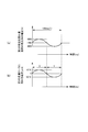
図4(a)は、第1の帯電ローラ3aに印加される変動電圧を示す。又、図4(b)は、第1の帯電位置C1を通過した直後(第1の帯電ローラ3aで帯電させた後)の感光体1の電位を示す。
図4(a)に示すように、第1の帯電ローラ3aに印加される変動電圧は、時間の関数である。本実施例では、画像形成時に第1の帯電ローラ3aに印加される変動電圧は、-1200Vを中心として、±100Vの範囲で変動させられる。又、この電圧の波形は、周期(T)が130msの正弦波である。
そして、上述のような電圧が第1の帯電ローラ3aに印加されることにより、第1の帯電位置C1を通過した直後の感光体1の表面には、図4(b)に示すような電位が形成されることになる。即ち、図4(b)に示すように、第1の帯電ローラ3aにより、感光体1の表面には、中央値が-800V、変動幅が±100V、感光体1の帯電極性側における最大値が-900V、最小値が-700V、周期(T)が130msの電位(変動電位)が形成される。このように、第1の帯電ローラ3aによって、感光体1の周方向に波状に変動する帯電電位が形成される。
図5は、第2の帯電位置C2に到達する直前(第2の帯電ローラ3bで帯電させる前)の感光体1の電位を示す。本実施例では、感光体1の帯電電位の暗減衰は、第1の帯電位置C1と第2の帯電位置C2との間で、約100Vである。従って、第2の帯電位置C2に到達する直前の感光体1の表面には、中央値が-700V、変動幅が±100V、感光体1の帯電極性側における最大値が-800V、最小値が-600Vの電位(変動電位)が形成されている。
本実施例では、画像形成中に、第1の帯電ローラ3aで形成した感光体1の電位を用いて、第2の帯電ローラ3bに放電による正負両方向の電流を交互に流し、第2の帯電ローラ3bの表面に付着したトナーや外添剤などの付着物(汚れ)の付着量を低減する。より詳細に説明すると、主に第2の帯電ローラ3bと感光体との接触部の感光体回転方向上流に存在する放電が発生する微小空間である放電ギャップで上記の放電電流が交互に流れる。
そのために、第2の帯電位置C2に到達する直前の感光体1の電位(PreVD)と、第2の帯電ローラ3bに印加される直流電圧の電位(Vdc)との差分(=PreVD-Vdc)が、負側の値と正側の値とに交互に切り替わるようにする。
尚、第1の帯電ローラ3aで形成された感光体1の電位と第2の帯電ローラ3bに流れる電流との関係については、後述して更に詳しく説明する。
ここで、第2の帯電位置C2に到達する直前の感光体1の電位と、第2の帯電ローラ3bに印加される直流電圧の電位との差分が、負側の値である時間をX(s)、正側の値である時間をY(s)とする。即ち、第1の帯電ローラ3aに帯電されて第2の帯電ローラ3bが帯電する位置に到達する感光体1の表面の電位が第2の帯電ローラ3bに印加される直流電圧よりも小さい値となる時間をX(s)、大きい値となる時間をY(s)とする。本実施例では、XとYは共に65msであり、同じ時間である。
そして、第2の帯電ローラ3b上の付着物を除去するために、第1の帯電ローラ3aで形成する感光体1の電位の変化(変動電位)は、以下の2条件を考慮して設定することが好ましい。
・第1の条件
第2の帯電ローラ3b上の付着物を除去するために、第2の帯電ローラ3bと感光体1との接触部近傍における少なくとも第2の帯電ローラ3bの上流ギャップ内を感光体の表面が通過する時間内で、第2の帯電ローラ3bに流れる電流の方向(正方向又は負方向)が切り替わらないように設定する。ここで、上述のように、感光体1の回転方向における第2の帯電ローラ3bと感光体1との接触部で、帯電処理が行われ、又電流が流れるものと擬制できる。従って、第2の帯電ローラ3b上の付着物を除去するためには、第2の帯電ローラ3bと感光体1との接触時間内で、第2の帯電ローラ3bに流れる電流の方向(正方向又は負方向)が切り替わらないように設定すればよい。そのためには、「X」及び「Y」を、第2の帯電ローラ3bと感光体1との接触時間よりも長くすればよい。従って、感光体1の回転方向における第2の帯電ローラ3bと感光体1との接触幅をW(mm)、感光体1の周速度をPS(mm/s)としたとき、次の関係式満たすように設定することが好ましい。
X>(W/PS)、Y>(W/PS)
例えば、本実施例では、第2の帯電ローラ3bと感光体1との接触幅Wは2(mm)であり、感光体1の周速度PSは850mm/secであるため、W/PS=2.35msecとなる。
第2の帯電ローラ3b上の付着物を除去するために、第2の帯電ローラ3bと感光体1との接触部近傍における少なくとも第2の帯電ローラ3bの上流ギャップ内を感光体の表面が通過する時間内で、第2の帯電ローラ3bに流れる電流の方向(正方向又は負方向)が切り替わらないように設定する。ここで、上述のように、感光体1の回転方向における第2の帯電ローラ3bと感光体1との接触部で、帯電処理が行われ、又電流が流れるものと擬制できる。従って、第2の帯電ローラ3b上の付着物を除去するためには、第2の帯電ローラ3bと感光体1との接触時間内で、第2の帯電ローラ3bに流れる電流の方向(正方向又は負方向)が切り替わらないように設定すればよい。そのためには、「X」及び「Y」を、第2の帯電ローラ3bと感光体1との接触時間よりも長くすればよい。従って、感光体1の回転方向における第2の帯電ローラ3bと感光体1との接触幅をW(mm)、感光体1の周速度をPS(mm/s)としたとき、次の関係式満たすように設定することが好ましい。
X>(W/PS)、Y>(W/PS)
例えば、本実施例では、第2の帯電ローラ3bと感光体1との接触幅Wは2(mm)であり、感光体1の周速度PSは850mm/secであるため、W/PS=2.35msecとなる。
尚、「XとYの和」は、第2の帯電ローラ3bに印加される交流電圧の周期よりも大きく設定する。これにより、詳しくは後述するように、第1の帯電ローラ3aに帯電されて第2の帯電位置C2に到達する感光体1の表面の電位と、第2の帯電ローラ3bに印加される直流電圧との電位差によって、第2の帯電ローラ3b上の付着物を除去することができる。例えば、本実施例では、XとYとの和は130ms(=65ms+65ms)であり、第2の帯電ローラ3bに印加される交流電圧の周期は約0.171ms(=1/5.86KHz)である。
・第2の条件
第1の帯電ローラ3aで形成した感光体1の変動電位が、第2の帯電位置C2に到達する際に、「X」、「Y」及び「XとYの和」のそれぞれと、第2の帯電ローラ3bの回転周期とが、互いに非整数倍の関係になるように設定することが好ましい。「X」及び「Y」のそれぞれと、第2の帯電ローラ3bの回転周期とを互いに非整数倍の関係にする理由は、第2の帯電ローラ3bに印加する直流電圧と第2の帯電位置C2に到達する感光体1の電位の電位差が、第2の帯電ローラ3bの回転毎に異なる電位差となるようにするためである。又、「XとYの和」と第2の帯電ローラ3bの回転周期とを互いに非整数倍の関係にする理由は、第2の帯電ローラ3bに流れる電流の方向(正方向又は負方向)が切り替わる部分、即ち、電流が流れない部分と、第2の帯電ローラ3bの回転周期とをずらすためである。
第1の帯電ローラ3aで形成した感光体1の変動電位が、第2の帯電位置C2に到達する際に、「X」、「Y」及び「XとYの和」のそれぞれと、第2の帯電ローラ3bの回転周期とが、互いに非整数倍の関係になるように設定することが好ましい。「X」及び「Y」のそれぞれと、第2の帯電ローラ3bの回転周期とを互いに非整数倍の関係にする理由は、第2の帯電ローラ3bに印加する直流電圧と第2の帯電位置C2に到達する感光体1の電位の電位差が、第2の帯電ローラ3bの回転毎に異なる電位差となるようにするためである。又、「XとYの和」と第2の帯電ローラ3bの回転周期とを互いに非整数倍の関係にする理由は、第2の帯電ローラ3bに流れる電流の方向(正方向又は負方向)が切り替わる部分、即ち、電流が流れない部分と、第2の帯電ローラ3bの回転周期とをずらすためである。
また、第2の帯電ローラ3b上に付着する正極性および負極性両方の付着物を均一に除去するためには、X≒Yとすることが好ましい。
このように設定にすることで、第2の帯電ローラ3bに、正負両方向の電流を偏ることなく切り替えて流すことができ、第2の帯電ローラ3b上の付着物を均一に除去することできる。
本実施例では、X、Yを共に65msとして、第2の帯電ローラ3bの回転周期の1.25倍に設定した。又、XとYの和は、第2の帯電ローラ3bの回転周期の2.5倍とした。
また、XとYの和は、1枚の記録材に対応するトナー画像が形成される感光体上の領域が第2の帯電ローラ3bを通過する時間よりも短い方が好ましい。1枚の画像形成のみを実行する場合においても、第2の帯電ローラ3b上の付着物を均一に除去することができるからである。たとえば、本実施例で1枚のA4サイズの記録材の長手方向が感光体の回転方向に対応するトナー画像が形成される場合に感光体上の領域が第2の帯電ローラ3bを通過する時間は、PSが850mm/sec、A4サイズの短手方向は210mmであるため、約247msとなる。
また、画像形成装置100では複数種類のサイズの記録材Pを用いることが可能であるため、画像形成装置100で用いる最小サイズの1枚の記録材Pに対応するトナー画像が形成される感光体上の領域が第2の帯電ローラ3bを通過する時間よりもXとYの和を短く設定しても良い。
尚、本実施例では、第1の帯電ローラ3aに印加する電圧の形状として正弦波を用いているが、三角波などの電圧でもよい。
5-2.第2の帯電ローラの帯電動作
次に、第2の帯電ローラ3bによる帯電動作について説明する。第2の帯電ローラ3bは、直流電圧と交流電圧とが重畳された振動電圧が印加されることで、感光体1を帯電させる。
次に、第2の帯電ローラ3bによる帯電動作について説明する。第2の帯電ローラ3bは、直流電圧と交流電圧とが重畳された振動電圧が印加されることで、感光体1を帯電させる。
図6は、第2の帯電位置C2に到達する直前の感光体1の電位と、第2の帯電位置を通過した直後(第2の帯電ローラ3bで帯電させた後)の感光体1の電位との関係を示す。
画像形成時に第2の帯電ローラ3bに印加される交流電圧は、ピーク間電圧Vppが1200V、周波数が5.86KHzである。又、画像形成時に第2の帯電ローラ3bに印加される直流電圧は、-700Vである。この直流電圧は、第2の帯電位置C2に到達する直前の感光体1の電位の中央値と同電位である。
このとき、第2の帯電位置C2に到達する直前の感光体1の電位(PreVD)と、第2の帯電ローラ3bに印加される直流電圧の電位(Vdc)との差分(=PreVD-Vdc)は、交互に負側の値、正側の値となる。そして、第2の帯電位置C2に到達する直前の感光体1の電位と、第2の帯電ローラ3bに印加される直流電圧の電位と差分の負側の最大値、正側の最大値は、次のようになる。
負側の最大値:(-800)-(-700)=-100(V)
正側の最大値:(-600)-(-700)=+100(V)
又、図6に示すように、第2の帯電位置C2に到達する直前の感光体1の電位によらず、第2の帯電位置C2を通過した直後の感光体1の電位(VD)は-700Vとなる。
負側の最大値:(-800)-(-700)=-100(V)
正側の最大値:(-600)-(-700)=+100(V)
又、図6に示すように、第2の帯電位置C2に到達する直前の感光体1の電位によらず、第2の帯電位置C2を通過した直後の感光体1の電位(VD)は-700Vとなる。
5-3.第2の帯電ローラに流れる電流
次に、第2の帯電ローラ3bに流れる電流について説明する。
次に、第2の帯電ローラ3bに流れる電流について説明する。
図7(a)は、第2の帯電位置C2に到達する直前の感光体1の電位を示す。図7(b)は、第2の帯電ローラ3bに流れる電流を示す。又、図7(b)中のX、Yはそれぞれ、上述の通りの時間を示す。即ち、Xは、第2の帯電位置C2に到達する直前の感光体1の電位(PreVD)と、第2の帯電ローラ3bに印加される直流電圧の電位(Vdc)との差分(=PreVD-Vdc)が、負側の値である時間であり、Yは、該差分が正側の値である時間である。
図7(b)より、Xの期間とYの期間とでは、第2の帯電ローラ3bと感光体1との間に流れる電流の方向は逆方向となる。又、第2の帯電ローラ3bに流れる電流の変化の周期(T)は130msである。この周期(T)は、第1の帯電ローラ3aに印加される変動電圧の周期(T)、及び第2の帯電位置C2に到達する直前の感光体1の電位の周期(T)と同じである。
本実施例では、Xの期間で第2の帯電ローラ3bに流れる電流の正方向の最大値は87.5μAであり、Yの期間で流れる電流の負方向の最大値は-87.5μAである。
5-4.第2の帯電ローラ上の付着物の低減作用
次に、第2の帯電ローラ3b上の付着物の低減作用について更に詳しく説明する。
図8は、第2の帯電ローラ3bに流れる電流の方向と、第2の帯電ローラ3bの表面に付着したトナーや外添剤などの付着物の帯電極性との関係を示す。図8(a)は、第2の帯電ローラ3bと感光体1との間に流れる電流が正方向の場合を示す。即ち、図8(a)は、図7(b)におけるXの期間を示す。又、図8(b)は、第2の帯電ローラ3bと感光体1との間に流れる電流が負方向の場合を示す。即ち、図8(b)は、図7(b)におけるYの期間を示す。
次に、第2の帯電ローラ3b上の付着物の低減作用について更に詳しく説明する。
図8は、第2の帯電ローラ3bに流れる電流の方向と、第2の帯電ローラ3bの表面に付着したトナーや外添剤などの付着物の帯電極性との関係を示す。図8(a)は、第2の帯電ローラ3bと感光体1との間に流れる電流が正方向の場合を示す。即ち、図8(a)は、図7(b)におけるXの期間を示す。又、図8(b)は、第2の帯電ローラ3bと感光体1との間に流れる電流が負方向の場合を示す。即ち、図8(b)は、図7(b)におけるYの期間を示す。
本実施例では、第2の帯電ローラ3bに流れる電流を所定の周期(T=130ms)で切り替え、第2の帯電ローラ3b上の正極性に帯電した付着物と負極性に帯電した付着物の両方を、第2の帯電ローラ3aに流れる電流の向きに応じて感光体1側に移動させる。
・Xの期間での付着物の移動
図8(a)では、第2の帯電ローラ3b側から感光体1側に電流が流れる。即ち、第2の帯電ローラ3bと感光体1との間で相対的に第2の帯電ローラ3b側が正極性側に高い電位であるため、第2の帯電ローラ3b側から感光体1側に電流が流れる。これにより、感光体1上の正極性に帯電した付着物は、第2の帯電ローラ3bに付着することなく第2の帯電位置C2を通過する。一方、感光体1上の負極性に帯電した付着物は、第2の帯電ローラ3bに回収される。
図8(a)では、第2の帯電ローラ3b側から感光体1側に電流が流れる。即ち、第2の帯電ローラ3bと感光体1との間で相対的に第2の帯電ローラ3b側が正極性側に高い電位であるため、第2の帯電ローラ3b側から感光体1側に電流が流れる。これにより、感光体1上の正極性に帯電した付着物は、第2の帯電ローラ3bに付着することなく第2の帯電位置C2を通過する。一方、感光体1上の負極性に帯電した付着物は、第2の帯電ローラ3bに回収される。
・Yの期間での付着物の移動
図8(b)では、感光体1側から第2の帯電ローラ3b側に電流が流れる。即ち、第2の帯電ローラ3bと感光体1との間で相対的に感光体1側が正極性側に高い電位であるため、感光体1側から第2の帯電ローラ3b側に電流が流れる。これにより、第2の帯電ローラ3b上の負極性に帯電した付着物は、感光体1に戻される。一方、感光体1上の正極性に帯電した付着物は、第2の帯電ローラ3bに付着する。
図8(b)では、感光体1側から第2の帯電ローラ3b側に電流が流れる。即ち、第2の帯電ローラ3bと感光体1との間で相対的に感光体1側が正極性側に高い電位であるため、感光体1側から第2の帯電ローラ3b側に電流が流れる。これにより、第2の帯電ローラ3b上の負極性に帯電した付着物は、感光体1に戻される。一方、感光体1上の正極性に帯電した付着物は、第2の帯電ローラ3bに付着する。
本実施例では、図8(a)、(b)の動作を所定の周期(T)で繰り返すことで、第2の帯電ローラ3bへの正極性又は負極性に帯電したトナーや外添剤などの付着物の蓄積を低減することができる。又、第2の帯電ローラ3b上の付着物の帯電極性が正極性又は負極性に過剰に偏ることがないため、画像形成を行えない特別の清掃モードを設けなくても、長期の連続画像形成が可能となる。そのため、画像形成装置100のダウンタイム(清掃動作や調整動作のために画像出力ができない時間)が低減されて生産性の向上を図ることができる。
第2の帯電ローラ3bへの付着物の蓄積が低減されるので、一度に第2の帯電ローラ3bから感光体1に移動させられる付着物の量は比較的少ない。従って、感光体1に移動させられた付着物が画像形成を阻害することはない。この感光体1に移動させられた付着物の多くは、前述のように、その後現像装置11で回収されるか、転写部Nにおいて記録材Pに転写されるか、又は転写部Nを通過した後にクリーニング装置15によって感光体1上から除去されて回収される。
尚、上述のような動作中に、第1、第2の清掃ローラ4a、4bは、第1、第2の帯電ローラ3a、3bとの接触回転動作により、前述のように第1、第2の帯電ロ-ラ3a、3bの表面の付着物を散らす作用と、付着力の低減させる作用をなしている。
更に説明すると、従来の複数の帯電ローラを用いる構成では、帯電電位ムラの低減に注目したものが多い。上流側の第1の帯電ローラで感光体に所定の帯電電位(PreVD)を形成し、下流側の第2の帯電ローラに交流電圧と直流電圧との重畳電圧を印加して放電によって帯電処理を行うことで、電位ムラの低減能力は高くなる。特に、この観点からは、第2の帯電ローラに印加する直流電圧の電位(Vdc)と、第1の帯電ローラで感光体に形成したPreVDとを等しくする条件が良い(PreVD=Vdc)。
しかし、このように「PreVD=Vdc」の条件にすると、第2の帯電ローラには直流電流が殆ど流れない(Idc≒0μA)。そのため、交流放電(正負両極性の放電が生じる)により、正極性に帯電された荷電粒子と負極性に帯電された荷電粒子の両方が、第2の帯電ローラに付着することになる。第2の帯電ローラの表面で交流放電により帯電された正負両極性の帯電粒子が付着してくる。又、第2の帯電ローラ上の付着物の極性が正負両方なので、逆バイアスの印加によってクリーニングしようとすると、正負両極性のバイアスの印加が必要となる。そのため、逆バイアスを印加するクリーニングシーケンスを実行しようとすれば、ダウンタイムが長くなり、生産性が低下することが懸念される。
そこで、本実施例では、画像形成中に、第1の帯電ローラに印加する電圧を周期的に変化させ、所定の直流電圧が印加される第2の帯電ローラに対して、感光体の周期的に変動するPreVDを供給する。即ち、第1の帯電ローラによって直流放電による感光体の帯電処理を行い、第1の帯電ローラに印加する直流電圧を直流放電領域で変化させる。これにより、第2の帯電ローラの表面で、放電電流を、正負に周期的に変化させる。その結果、画像形成中に、第2の帯電ローラによって帯電処理した後の感光体の帯電電位ムラを発生させることなく、第2の帯電ローラの表面に付着した正負両極性の荷電粒子を、放電の方向に沿って感光体側に移動させることができる。そのため、第2の帯電ローラの表面のトナーや外添剤などの付着物を低減させることが可能となる。つまり、画像形成中に第2の帯電ローラ上に正負に帯電したトナ-や外添剤が連れまわらずに入れ替わり、付着量を低減することが可能となる。
又、第2の帯電ローラの回転周期と異なる位相で、第1の帯電ローラに印加する電圧を変化させることで、第2の帯電ローラ上の正負両極性の荷電粒子を均等に除去できる。即ち、第1の帯電ローラで感光体に形成するPreVDの周期は、第2の帯電ローラの回転周期とずらし、第2の帯電ローラの同じ部位に対し同電位のPreVDが毎回来ないようにする。例えば、第2の帯電ローラの回転周期をTsとするとき、第1の帯電ローラに印加する変動電圧の可変周期(T)を、T=2Ts/(2n-1)[ただし、nは0以上の整数]とする。
尚、帯電ローラに直流電圧を印加した場合の放電開始電圧をVthとする。又、第2の帯電ローラに到達する感光体の帯電電位の、感光体の帯電極性側における最大値をVHI、感光体の帯電極性側における最小値をVLOとする。又、第2の帯電ローラに印加する直流電圧の電位をVdcとする。このとき、上述のような画像形成時の帯電動作においては、|VHI-VLO|<2Vth、|VHI|>|Vdc|、及び、|VLO|<|Vdc|の関係を満たすようにする。これにより、第2の帯電位置を通過した後の感光体の帯電電位を、第2の帯電ローラに印加される直流電圧の電位に安定して収束させることができる。
このように、画像形成装置100は、回転可能な感光体1と、感光体1に対して接触又は近接する第1の帯電ローラ3aと、感光体1の回転方向において第1の帯電ローラ3aよりも下流側で前記感光体に対して接触又は近接する第2の帯電ローラ3bとを有する。又、画像形成装置100は、第1の帯電ローラ3aに電圧値が変動する変動電圧を印加する第1の電源S1と、第2の帯電ローラ3bに直流電圧と交流電圧とを重畳させた電圧を印加する第2の電源S2と、を有する。更に、画像形成装置100は、画像形成中に、第1の電源S1から第1の帯電ローラ3aに印加する変動電圧を変動させる制御手段200を有する。制御手段200は、次のようにして、第1の帯電ローラ3aに印加する変動電圧を変動させる。即ち、第1の帯電ローラ3aで帯電させられて第2の帯電ローラ3bで感光体1を帯電させる位置に到達する感光体1の電位と、第2の帯電ローラ3bに印加される直流電圧の電位との大小関係が、交互に切り替わるようにする。又、より詳細には、制御手段200は、画像形成中に、第1の電源S1から第1の帯電ローラ3aに印加する変動電圧を、感光体1の帯電極性側において放電開始電圧より大きい電圧値の範囲で変動させる。そして、一実施態様では、画像形成中に、第1の帯電ローラ3aに印加される変動電圧の中央値と第2の帯電ローラ3bに印加される直流電圧の電位とは略等しい。
本実施例では、第1の帯電ローラ3aに変動電圧を印加する第1の電源S1として電圧値を変動させることが可能な直流電圧源を用いることにより、コストの低減を実現している。本実施例のように第1の電源S1として片側の極性の電圧を出力する直流電源を用いた場合の変動電圧の変動量上限について検討すると、感光体を帯電させることができる電圧値の下限値である放電開始電圧Vthが実質的に変動電圧の下限値となり、その場合、第2の帯電ローラ3bの付着物を均等に除去するためには変動電圧の中央値と前述した変動電圧の下限値であるVthとの電位差と同じ電位差となる電圧を最大値の上限とするのが好ましい。その場合、第2の帯電ローラに到達する感光体の帯電電位の変動量である|VHI-VLO|は、|VHI-VLO|<2×|Vdc|の関係を満たす。
また、変動電圧の変動量下限については、付着物を除去する効果を得るためには少なくとも第1の帯電ローラ3aで感光体を変動電位の中央値の電位になるように帯電する際に流れる電流の1割以上の電流が第2の帯電ローラ3bと感光体との間に流れる感光体の電位になるようすることが好ましく、例えば第1の帯電ローラ3aで感光体を-800Vに帯電する場合に第1の帯電ローラと感光体との間に流れる電流が-700μAであった場合、第1の帯電ローラ3aと第2の帯電ローラ3bの抵抗値が同じであるとした場合少なくとも70μA以上の電流が第2の帯電ローラ3bと感光体との間に流れるようにするためには、感光体の電位と第2の帯電ローラ3bの直流電圧値との電位差が80V以上になるように変動電圧の変動量を設定するのが好ましい。
6.制御フロー
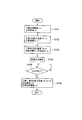
次に、図9を参照して、本実施例における画像形成動作時の制御フローの概略について説明する。CPU200は、画像形成信号の入力に伴い、画像形成装置100を、以下の手順で制御する。
次に、図9を参照して、本実施例における画像形成動作時の制御フローの概略について説明する。CPU200は、画像形成信号の入力に伴い、画像形成装置100を、以下の手順で制御する。
CPU200は、画像形成信号が入力されると、感光体1を回転駆動させると共に、帯電前露光ランプ17によって感光体1を露光させる(S101)。
次に、CPU200は、感光体1が定常回転に到達したことを検知したタイミングで、第1の高圧電源S1から第1の帯電ローラ3aに所定の周期(T)の変動電圧(直流電圧)を出力させて、感光体1を帯電させる(S102)。
次に、CPU200は、第2の高圧電源S2から第2の帯電ローラ3bに、直流電圧と交流電圧とを重畳した振動電圧を出力させて、感光体1を帯電させる(S103)。
次に、CPU200は、露光装置13を制御して画像形成を開始する(S104)。その後、CPU200が画像形成終了命令を出すまで、画像形成動作が継続される(S105)。
CPU200は、所定のジョブ(一の画像形成開始指示による単一又は複数の記録材に対する一連の画像形成動作)が完了すると、画像形成終了命令を出す。その後、CPU200は、第1、第2の高圧電源S1、S2の高圧出力、帯電前露光ランプ17の点灯、感光体1の回転駆動を順次停止させ、一連の画像形成動作を終了する(S106)。
以上の制御フローにより、画像形成動作中に、第1の帯電ローラ3aを用いて所定の周期(T)の感光体1の変動電位が形成される。又、第2の帯電ローラ3bにおいて、帯電前の感光体1の電位と第2の帯電ローラ3bに印加される直流電圧の電位とにより、所定の周期(T)で交互に正負両方向の電流が流れる。
本実施例において、トナー像を形成するために第1の帯電ローラ3aおよび第2の帯電ローラ3bで感光体を帯電させるときとは、少なくとも以上の制御フローにおけるS103~S106が該当する。
7.制御タイミング
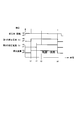
次に、図10を参照して、本実施例における画像形成時動作について説明する。
感光体1の回転動作が安定した後、時点t1(約500ms後)において、第1の高圧電源S1から第1の帯電ローラ3aに所定の周期(T)の変動電圧(直流電圧)が出力されて、第1の帯電ローラ3aによる感光体1の帯電処理が行われる。
次に、図10を参照して、本実施例における画像形成時動作について説明する。
感光体1の回転動作が安定した後、時点t1(約500ms後)において、第1の高圧電源S1から第1の帯電ローラ3aに所定の周期(T)の変動電圧(直流電圧)が出力されて、第1の帯電ローラ3aによる感光体1の帯電処理が行われる。
その後、時点t2(約700ms)において、第2の高圧電源S2から第2の帯電ローラ3bに直流電圧と交流電圧とが重畳された振動電圧が出力されて、第2の帯電ロ-ラ3bによる感光体1の帯電処理が行われる。
その後、時点t3(約900ms)から画像形成が開始される。
その後、時点t4においてジョブが終了した後、第1、第2の高圧電源S1、S2の高圧出力、帯電前露光ランプ17の点灯、感光体1の回転駆動が順次停止され、一連の画像形成動作が終了する。
その後、時点t3(約900ms)から画像形成が開始される。
その後、時点t4においてジョブが終了した後、第1、第2の高圧電源S1、S2の高圧出力、帯電前露光ランプ17の点灯、感光体1の回転駆動が順次停止され、一連の画像形成動作が終了する。
以上のように、画像形成中に第2の帯電ローラ3b上の付着物による電位ムラの発生が抑制されるので、ダウンタイムが低減されて生産性の向上を図ることができる。即ち、本実施例では、画像形成中に、第1の帯電ローラ3aの変動電圧を用いて感光体1の電位を変化させる。そして、第2の帯電ローラ3bの直流電圧の電位との電位差を用いて、第2の帯電ローラ3bに正負両方向の電流を交互に流す。これにより、第2の帯電ローラに付着した汚れ物質を除去することができる。画像形成を中断するなどして特別に清掃モ-ドを設ける必要がない。そのため、ダウンタイムを低減して、画像形成装置の生産性を高めることが可能となる。又、複数の帯電ローラを用いる構成において、最下流側に配置した帯電ローラの表面が汚れることによる帯電不良を防止することで、画像品質の安定性が向上できる。
以上、本実施例によれば、画像形成を行えない特別な期間を設けて帯電部材の清掃を行わなくても、帯電部材へのトナーなどの付着物の蓄積を抑制することができ、生産性の向上を図ることができる。
次に、本発明の他の実施例について説明する。本実施例の画像形成装置の基本的な構成及び動作は実施例1のものと同じである。従って、本実施例の画像形成装置において実施例1の画像形成装置のものと同一又はそれに相当する機能、構成を有する要素には同一符号を付して詳しい説明は省略する。
本実施例では、第1の帯電ローラ3aに印加する帯電電圧として、実施例1と同様の変動電圧に対して、変動電圧よりも周期が短い交流電圧を重畳させた、振動電圧を印加する。この変更により、第1の帯電ローラ3aで形成する感光体1の電位の安定性が向上する。これにより、実施例1と同様の効果を得つつ、より安定した感光体1の帯電電位によって高画質化を図ることが可能となる。
図11は、本実施例の画像形成装置100の要部の構成を示す模式的な断面図である。又、図12は、本実施例の画像形成装置100の要部の制御態様を示すブロックである。
本実施例では、第1の帯電ローラ3aの芯金31aには、第1の電源としての第1の高圧電源S3が接続されている。第1の高圧電源S3は、変動電圧を供給する変動電圧電源部S3aと交流電圧を供給する交流電源部S3bとを備え、第1の帯電ローラ3aに変動電圧と交流電圧とを重畳した振動電圧を印加することができる。第1の高圧電源S3は、高圧出力制御部300に接続されている。
尚、本実施例では、第1の高圧電源S3は、第2の高圧電源S2と共通の構成である。
尚、本実施例では、第1の高圧電源S3は、第2の高圧電源S2と共通の構成である。
次に、第1の帯電ローラ3aによる帯電動作について説明する。
図13(a)は、第1の帯電ローラ3aに印加される変動電圧の時間変化を示す。又、図13(b)は、第1の帯電位置C1を通過した直後の感光体1の電位の時間変化を示す。
図13(a)は、第1の帯電ローラ3aに印加される変動電圧の時間変化を示す。又、図13(b)は、第1の帯電位置C1を通過した直後の感光体1の電位の時間変化を示す。
図13(a)に示すように、第1の帯電ローラ3aには、中央値が-800V、変動幅が±100Vの変動電圧が印加される。又、この電圧の波形は、周期(T)が130msの正弦波である。
又、第1の帯電ローラ3aには、上記変動電圧に対して、ピーク間電圧Vppが1200V、周波数5.86KHzの交流電圧が重畳されて印加される。即ち、第1の帯電ローラ3aには、中央値が-800Vの振動電圧が印加される。
そして、この電圧の印加により、第1の帯電位置C1を通過した直後の感光体1の表面には、図13(b)に示すような電位が形成される。即ち、中央値が-800V、変動幅が±100V、感光体1の帯電極性側における最大値が-900V、最小値が-700V、周期(T)が130msの電位(変動電位)が形成される。このように、第1の帯電ローラ3aによって、感光体1の周方向に波状に変動する帯電電位が形成される。
尚、第2の帯電位置C2に到達する直前の感光体1の電位の時間変化は、実施例1と同様となる。又、第2の帯電ローラ3bに印加する電圧の設定は、実施例1と同じである。
図14は、本実施例における画像形成動作時制御フローの概略を示す。
図14のフローチャートのステップS201~S206の処理は、実施例1にて説明した図9のフローチャートのステップS101~S106の処理と同様である。ただし、S202において、第2の高圧電源S3から第1の帯電ローラ3aに、変動電圧に交流電圧を重畳させ振動電圧を出力する点が異なる。
以上、本実施例によれば、実施例1よりも電位ムラが小さく、安定した感光体1の電位の形成が可能となる。
次に、本発明の他の実施例について説明する。本実施例の画像形成装置の基本的な構成及び動作は実施例1のものと同じである。従って、本実施例の画像形成装置において実施例1の画像形成装置のものと同一又はそれに相当する機能、構成を有する要素には同一符号を付して詳しい説明は省略する。
本実施例では、第1の帯電ローラ3aで形成した感光体1の変動電位の中心値を、第2の帯電ローラ3bに印加する直流電圧の電位に対して、正極性側又は負極性側の一方向にずらした値に設定する。これにより、正極性又は負極性の一方に帯電しやすい感光体1上のトナーや外添剤などの付着物の除去効率が向上する。
本実施例では、第2の帯電位置C2に到達する直前の感光体1の電位(PreVD)と、第2帯電ローラ3bに印加される直流電圧の電位(Vdc)との差分(=PreVD-Vdc)の絶対値の最大値が、負側の値よりも正側の値の方が大きくなるように設定した。
図15(a)は、第2の帯電位置C2に到達する直前の感光体1の電位の時間変化を示す。又、図15(b)は、第2の帯電ローラ3bに流れる電流の時間変化を示す。
図15(a)に示すように、第2の帯電位置C2に到達する直前の感光体1の電位は、中央値が-700Vで、感光体1の帯電極性側における最大値が-800V、最小値が-550Vである。即ち、本実施例では、Xに対応する期間よりも、Yに対応する期間の感光体1の電位の振幅を大きくした。
尚、第2の帯電ローラ3bに印加する電圧の設定は、実施例1と同じであり、第2の帯電ローラ3bに印加される直流電圧は-700Vである。
そして、第2の帯電位置C2に到達する直前の感光体1の電位と、第2の帯電ローラ3bに印加される直流電圧の電位と差分の負側の最大値、正側の最大値、及びそれらの絶対値間の関係は、次のようになる。
負側の最大値:(-800)-(-700)=-100(V)
正側の最大値:(-550)-(-700)=+150(V)
|負側の最大値|<|正側の最大値|=|-100|<|150|
尚、実施例1と同様に、XとYは共に65msとして、第2の帯電ローラ3bの回転周期の1.25倍とした。
負側の最大値:(-800)-(-700)=-100(V)
正側の最大値:(-550)-(-700)=+150(V)
|負側の最大値|<|正側の最大値|=|-100|<|150|
尚、実施例1と同様に、XとYは共に65msとして、第2の帯電ローラ3bの回転周期の1.25倍とした。
これにより、図15(b)に示すように、第2の帯電ローラ3bに流れる電流は、正方向の電流よりも、負方向の電流が大きくなる。本実施例では、Xの期間で第2の帯電ローラ3bに流れる電流の正方向の最大値は87.5μAであり、Yの期間で第2の帯電ローラ3bに流れる電流の負方向の最大値は-130μAである。
即ち、本実施例では、画像形成中に交互に切り替わる感光体1の電位と第2の帯電部材3bに印加される直流電圧の電位との差分の負側の値と正側の値とで、該差分の絶対値の最大値が異なる。
このように設定することで、第2の帯電ローラ3bに流れる電流は、正方向の電流よりも負方向の電流の方が大きくなる。即ち、負極性に帯電した付着物を感光体1側に移動させやすくなる。そのため、第2の帯電位置C2を通過する感光体1上のトナーや外添剤などの付着物は、負極性側に偏らせることが可能となる。又、第2の帯電ローラ3bには、感光体1の変動電位により正方向の電流も流れるため、第2の帯電ローラ3bに、正極性に帯電した付着物が蓄積することも抑制することができ、安定した画像形成が可能である。
尚、本実施例では、第2の帯電ローラ3bに流れる電流は、正方向の電流よりも負方向の電流を大きくした。しかし、トナー、外添剤、感光体1の帯電極性に合わせて、正方向又は負方向のいずれを大きくするかや、正方向と負方向の電流の比は、適宜変更することができる。
次に、本発明の他の実施例について説明する。本実施例の画像形成装置の基本的な構成及び動作は実施例1のものと同じである。従って、本実施例の画像形成装置において実施例1の画像形成装置のものと同一又はそれに相当する機能、構成を有する要素には同一符号を付して詳しい説明は省略する。
本実施例では、第2の帯電位置C2に到達する直前の感光体1の電位と、第2の帯電ローラ3bに印加される直流電圧の電位との差分が負側の値である時間Xと、正側の値である時間Yとを異なる値に設定する(XとYとの比率を1:1からずらす)。これにより、正極性又は負極性の一方に帯電しやすい、感光体1上のトナーや外添剤などの付着物の除去効率が向上する。
本実施例では、第1の帯電ローラ3aで形成する感光体1の変動電位を、第2の帯電ローラ3bに流れる正方向の電流が負方向の電流よりも長い時間になるように設定した。
図16(a)は、第2の帯電位置C2に到達する直前の感光体1の電位の時間変化を示す。又、図16(b)は、第2の帯電ローラ3bに流れる電流の時間変化を示す。
図16(a)に示すように、第2の帯電位置C2に到達する直前の感光体1の電位は、中央値が-700V、変動幅が±50V、感光体1の帯電極性側における最大値が-750V、最小値が-650Vの変動電位である。
尚、第2の帯電ローラ3bに印加する電圧の設定は、実施例1と同じであり、第2の帯電ローラ3bに印加される直流電圧は-700Vである。
そして、第2の帯電位置C2に到達する直前の感光体1の電位と、第2の帯電ローラ3bに印加される直流電圧の電位との差分が負側の値となる時間Xと、正側の値となる時間Yとを異なる値として、XとYとの比率を2:1とした。本実施例では、Xを260ms、Yを130msとした。
これにより、第2の帯電ローラ3bに正方向の電流が流れる期間Xと、負方向の電流が流れる期間Yとの時間比率を2:1に偏らせた。本実施例では、Xの期間で第2の帯電ローラ3bに流れる正方向の電流の最大値は43μAであり、Yの期間で第2の帯電ローラ3bに流れる負方向の電流の最大値は-43μAである。
即ち、本実施例では、画像形成中に交互に切り替わる感光体1の電位と第2の帯電部材3bに印加される直流電圧の電位との差分が、負側の値となる時間をX(s)、正側の値となる時間をY(s)としたとき、XとYとの比率は、X又はYに偏っている。
このように設定にすることで、第2の帯電ローラ3bに正方向の電流が流れる時間を負方向の電流が流れる時間よりも長くできる。即ち、正極性に帯電した付着を感光体1側に移動させやすくなる。そのため、第2の帯電ローラ3bに感光体1上の正極性に帯電したトナーや外添剤などの付着物が蓄積することをより低減しやすくすることが可能となる。又、第2の帯電ローラ3bには、感光体1の変動電位により負方向の電流も流れるため、第2の帯電ローラ3bに、負極性に帯電した付着物が蓄積することも抑制することができ、安定した画像形成が可能である。
尚、本実施例では、第2の帯電ローラ3bに正方向電流が流れる時間を負方向の電流が流れる時間よりも大きくした。しかし、トナー、外添剤、感光体1の帯電極性に合わせて、正方向又は負方向のいずれが流れる時間を大きくするかや、正方向と負方向の電流が流れる時間の比は、適宜変更することができる。
又、正方向と負方向の電流が流れる時間X、Yの時間比率は、画像形成装置100に備えた、出力枚数カウンター700などを用いて、所定の出力枚数毎に変更するなどしてもよい。例えば、印刷開始後、A4横サイズで1000枚までの期間は、XとYの時間比率を2:1のように制御し、その後、xとYの時間比率を3:1のように切り替えるようにする。これにより、1000枚以上の連続出力条件では、第2の帯電ローラ3b上に蓄積する正帯電の付着物を更に低減することが可能となる。従って、正帯電極性の付着物が第2の帯電ローラ3bに蓄積することをより抑制できる効果が得られる。
次に、本発明の他の実施例について説明する。本実施例の画像形成装置の基本的な構成及び動作は実施例1のものと同じである。従って、本実施例の画像形成装置において実施例1の画像形成装置のものと同一又はそれに相当する機能、構成を有する要素には同一符号を付して詳しい説明は省略する。本実施例は、実施例4の変形例である。
本実施例では、実施例4の構成において、感光体1に形成する変動電位の感光体1の帯電極性側における最大値又は最小値を、正極性又は負極性の方向に各独立にずらした値に設定した。
本実施例では、第2の帯電位置C2に到達する直前の感光体1の電位の感光体1の帯電極性側における最大値又は最小値を独立に変更することで、第2の帯電ローラ3bに流れる正方向又は負方向の電流量を調整することができる。これにより、正極性又は負極性の一方に帯電しやすい感光体1上のトナーや外添剤などの付着物がある場合に、その帯電極性が偏る場合や付着量が多い場合でも、その除去効率を調整できる。
本実施例では、第1の帯電ローラ3aで形成する感光体1の変動電位の感光体1の帯電極性側における最大値を、実施例4よりも第2の帯電ローラ3bに印加される直流電圧の電位に対して負極性寄りに設定した。
本実施例では、実施例4にて説明した図16(a)に示す第2の帯電位置C2に到達する直前の感光体1の電位の時間変化において、感光体1の帯電極性側における最大値を、実施例4よりも負極性側に偏らせて-850Vに変更した。感光体1の帯電極性側における最小値は、実施例4と同じ-650Vのままとした。
尚、第2の帯電ローラ3bに印加する電圧の設定は、実施例1と同じであり、第2の帯電ローラ3bに印加される直流電圧は-700Vである。
これにより、実施例4にて説明した図16(b)に示す第2の帯電ローラ3bに流れる電流の時間変化において、Xの期間に流れる正方向の電流の最大値を、実施例4よりも大きくして86μAに変更した。Yの期間に流れる電流の最大値は、実施例4と同じ-43μAのままである。
これにより、実施例4よりも、第2の帯電ローラ3bに付着する正極性に帯電した付着物を低減することができる。
尚、本実施例では、感光体1の変動電位の感光体1の帯電極性側における最大値のみを大きくしたが、感光体1の帯電極性側における最小値のみを変更して第2の帯電ローラ3bに流れる負方向の電流を大きくしてもよい。
又、感光体1の変動電位の感光体1の帯電極性側における最大値又は最小値と、第2の帯電ローラ3bに印加される直流電圧との電位差は、画像形成装置100に用いるトナー、外添剤の極性などに応じて、適宜変更することができる。
次に、本発明の他の実施例について説明する。本実施例の画像形成装置の基本的な構成及び動作は実施例1のものと同じである。従って、本実施例の画像形成装置において実施例1の画像形成装置のものと同一又はそれに相当する機能、構成を有する要素には同一符号を付して詳しい説明は省略する。
本実施例では、感光体1上に形成する変動電位の感光体1の帯電極性側における最大値及び最小値を、所定の出力枚数毎に変更する。即ち、本実施例では、制御手段としてのCPU200が、画像形成枚数に基づいて第1の帯電ローラ3aに印加する変動電圧の最大値及び最小値を切り替える。これにより、感光体1に形成する変動電位の電位差を定期的に変更させて、第2の帯電ローラ3bに流れる正負両方向の電流の大きさを変更し、第2の帯電ローラ3b上の付着物の除去効果を向上させた。即ち、定期的に変動電位の変動幅を交互に切り替えることで、第2の帯電ローラ3bより感光体1に流れる正負方向の電流を定期的に増加させることができる。これにより、小さい変動電位では除去できなかった低帯電の正負に帯電した付着物を、定期的に大きな変動電流を与えることで除去できるようになる。従って、付着物の蓄積をより抑制することができ、付着物の除去効果が向上する。
実施例1では、図4(a)に示すように、第1の帯電ローラ3aに印加する変動電圧の変動幅を±100Vで固定としていた。これに対して、本実施例では、第1の帯電ローラ3aに印加する変動電圧の変動幅を、所定の出力枚数枚毎に切り替える。
本実施例では、第1の帯電ローラ3aに印加する変動電圧は、中央値を-1200Vとして、変動幅を、±75V、±150Vの2段階とした。そして、出力枚数カウンター700を用いて、画像出力枚数1000枚毎にこの変動幅の切り替えを行った。
尚、本実施例では、第1の帯電ローラ3aに印加する変動電圧の変動幅は、正極性側、負極性側を同じ変動幅で変更したが、正極性側と負極性側とで異なる変更幅で変更してもよい。
次に、図17を参照して、本実施例における画像形成動作時の制御フローについて説明する。
CPU200は、画像形成信号の入力に伴い、画像形成装置100を、以下の手順で制御する。
CPU200は、画像形成信号が入力されると、感光体1を回転駆動させると共に、帯電前露光ランプ17によって感光体1を露光させる(S301)。
次に、CPU200は、感光体1が定常回転に到達したことを検知したタイミングで、第1の高圧電源S1から第1の帯電ローラ3aに所定の周期(T)の変動電圧(直流電圧)を出力させて、感光体1を帯電させる(S302)。このとき、変動電圧の変動幅は、±75Vに設定する。
次に、CPU200は、第2の高圧電源S2から第2の帯電ローラ3bに、直流電圧と交流電圧とを重畳した振動電圧を出力させて、感光体1を帯電させる(S303)。
次に、CPU200は、動電位の切り替えに用いる、出力枚数カウンター700のカウント枚数Pを0にリセットする(S304)。
次に、CPU200は、露光装置13を制御して画像形成を開始する(S305)。
その後、CPU200は、カウント枚数Pが1000枚に到達したかを判定する(S306)。
S306で、1000枚未満と判定された場合、CPU200は、ジョブの終了を判定する(S307)。
S307にてジョブ終了と判定された場合は、CPU200は、第1、第2の高圧電源S1、S2の高圧出力、帯電前露光ランプ17の点灯、感光体1の回転駆動を順次停止させ、一連の画像形成動作を終了する(S308)。
又、S307でジョブ継続と判定された場合は、カウント枚数Pをカウントアップした後(S310)、S306に移行する。この動作が、ジョブが終了するまで繰り返される。
一方、S306で、1000枚以上と判定された場合、CPU200は、第1の帯電ローラ3aに印加する変動電圧の変動幅を±150Vに切り替え、カウンター700のカウント枚数Pを0にリセットする(S309)。引き続き、S307に移行して、CPU200は、ジョブの終了を判定する。
その後、ジョブ継続される場合、カウンター700のカウント枚数Pが1000枚に到達する毎に、変動幅は、±75V、±150Vが交互に切り替えられる。
以上の動作により、感光体1の変動電位の変動幅は、所定の出力枚数間隔で切り替えられる。即ち、本実施例では、制御手段200は、第2の帯電位置C2に到達する感光体1の電位と第2の帯電ローラ3bに印加される直流電圧の電位との差分の絶対値の最大値を、定期的に切り替える。これにより、第2の帯電ローラ3b上の付着物の除去効果が向上する。
尚、本実施例では、カウンター700によって計数された画像出力枚数に応じて第1の帯電ローラ3aに印加する変動電圧の変動幅を変更したが、これに限定されるものではない。例えば、タイマー600を用いて、画像形成時間、感光体1、第1、第2の帯電ローラ3a、3bなどの回転部材の回転時間、或いは第1、第2の帯電ローラ3a、3bへの電圧印加時間などを計測することができる。そして、その計測結果に応じて第1の帯電ローラ3aに印加する変動電圧の変動幅を変更してもよい。つまり、第1、第2の帯電部材3a、3bの使用量と相関する情報に応じて変更できればよい。
本発明は上記実施の形態に制限されるものではなく、本発明の精神及び範囲から離脱することなく、様々な変更及び変形が可能である。従って、本発明の範囲を公にするために以下の請求項を添付する。
本願は、2012年07月02日提出の日本国特許出願特願2012-148961及び2013年06月18日提出の日本国特許出願特願2013-127993を基礎として優先権を主張するものであり、その記載内容の全てをここに援用する。
1 感光体
2 帯電装置
3a 第1の帯電ローラ
3b 第2の帯電ローラ
S1 第1の高圧電源
S2 第2の高圧電源
S3 第1の高圧電源
2 帯電装置
3a 第1の帯電ローラ
3b 第2の帯電ローラ
S1 第1の高圧電源
S2 第2の高圧電源
S3 第1の高圧電源
Claims (4)
- 回転可能な感光体と、
前記感光体を帯電する第1の帯電ローラと、
前記感光体の回転方向において前記第1の帯電ローラよりも下流側で前記感光体を帯電する第2の帯電ローラと、
前記感光体の回転方向において前記第2の帯電ローラよりも下流側に配置され、前記第1の帯電ローラおよび前記第2の帯電ローラによって帯電された感光体の表面に潜像を形成し、潜像をトナーで現像してトナー像を形成するトナー像形成部と、
前記第1の帯電ローラに電圧値を変動させた変動電圧を印加する第1の電源と、
前記第2の帯電ローラに直流電圧と交流電圧とを重畳させた電圧を印加する第2の電源と、
トナー像を形成するために前記第1の帯電ローラおよび前記第2の帯電ローラで前記感光体を帯電させるとき、前記第1の帯電ローラに帯電されて前記第2の帯電ローラが帯電する位置に到達する前記感光体の電位と、前記第2の帯電ローラに印加される直流電圧値との大小関係が、交互に切り替わるように前記第1の電源から前記第1の帯電ローラに印加する前記変動電圧を変動させる制御手段とを有し、
トナー像を形成するために前記第1の帯電ローラおよび前記第2の帯電ローラで前記感光体を帯電させるとき、前記第1の帯電ローラに帯電されて前記第2の帯電ローラが帯電する位置に到達する前記感光体表面の電位が前記第2の帯電ローラに印加される直流電圧よりも小さい値となる時間をX(s)、大きい値となる時間をY(s)、前記感光体の周速度をPS(mm/s)、前記感光体の回転方向における前記第2の帯電ローラと前記感光体との接触幅をW(mm)としたとき、
X>(W/PS)、 Y>(W/PS)
の関係を満たし、
XとYの和は前記第2の帯電ローラに印加される交流電圧の周期よりも大きいことを特徴とする画像形成装置。 - トナー像を形成するために前記第1の帯電ローラおよび前記第2の帯電ローラで前記感光体を帯電させるとき、前記Xと前記第2の帯電ローラの回転周期、前記Yと前記第2の帯電ローラの回転周期、前記Xと前記Yの和と前記第2の帯電ローラの回転周期が互いに非整数倍の関係であることを特徴とする請求項1に記載の画像形成装置。
- 前記第1の帯電ローラに帯電されて前記第2の帯電ローラが帯電する位置に到達する前記感光体表面の電位の最大値をVHI、最小値をVLO、前記第2の帯電ローラに印加される直流電圧をVdcとしたとき、
|VHI-VLO|<2|Vdc|
の関係を満たすことを特徴とする請求項1に記載の画像形成装置。 - 前記制御手段は、画像形成枚数に基づいて前記変動電圧の最大値および最小値を切り替えることを特徴とする請求項1に記載の画像形成装置。
Priority Applications (1)
| Application Number | Priority Date | Filing Date | Title |
|---|---|---|---|
| US14/074,563 US8948636B2 (en) | 2012-07-02 | 2013-11-07 | Image forming apparatus comprising a plurality of charging rollers |
Applications Claiming Priority (4)
| Application Number | Priority Date | Filing Date | Title |
|---|---|---|---|
| JP2012-148961 | 2012-07-02 | ||
| JP2012148961 | 2012-07-02 | ||
| JP2013127993A JP2014029497A (ja) | 2012-07-02 | 2013-06-18 | 画像形成装置 |
| JP2013-127993 | 2013-06-18 |
Related Child Applications (1)
| Application Number | Title | Priority Date | Filing Date |
|---|---|---|---|
| US14/074,563 Continuation US8948636B2 (en) | 2012-07-02 | 2013-11-07 | Image forming apparatus comprising a plurality of charging rollers |
Publications (1)
| Publication Number | Publication Date |
|---|---|
| WO2014007091A1 true WO2014007091A1 (ja) | 2014-01-09 |
Family
ID=49881849
Family Applications (1)
| Application Number | Title | Priority Date | Filing Date |
|---|---|---|---|
| PCT/JP2013/067202 Ceased WO2014007091A1 (ja) | 2012-07-02 | 2013-06-24 | 画像形成装置 |
Country Status (3)
| Country | Link |
|---|---|
| US (1) | US8948636B2 (ja) |
| JP (1) | JP2014029497A (ja) |
| WO (1) | WO2014007091A1 (ja) |
Families Citing this family (3)
| Publication number | Priority date | Publication date | Assignee | Title |
|---|---|---|---|---|
| JP2019060905A (ja) * | 2017-09-22 | 2019-04-18 | キヤノン株式会社 | 帯電装置及び画像形成装置 |
| JP7071163B2 (ja) * | 2018-02-28 | 2022-05-18 | キヤノン株式会社 | 画像形成装置 |
| JP7154874B2 (ja) * | 2018-08-20 | 2022-10-18 | キヤノン株式会社 | 画像形成装置 |
Citations (6)
| Publication number | Priority date | Publication date | Assignee | Title |
|---|---|---|---|---|
| JPH0980874A (ja) * | 1995-09-18 | 1997-03-28 | Fuji Xerox Co Ltd | 画像形成装置 |
| JPH09222768A (ja) * | 1996-02-15 | 1997-08-26 | Fuji Xerox Co Ltd | 画像形成装置の帯電装置 |
| JPH09281773A (ja) * | 1996-02-15 | 1997-10-31 | Fuji Xerox Co Ltd | 帯電装置 |
| JPH10177291A (ja) * | 1996-12-19 | 1998-06-30 | Minolta Co Ltd | 画像形成装置 |
| JP2007114418A (ja) * | 2005-10-19 | 2007-05-10 | Kyocera Mita Corp | 画像形成装置 |
| JP2007334148A (ja) * | 2006-06-16 | 2007-12-27 | Fuji Xerox Co Ltd | 帯電装置及び画像形成装置 |
Family Cites Families (1)
| Publication number | Priority date | Publication date | Assignee | Title |
|---|---|---|---|---|
| JP5780772B2 (ja) * | 2011-02-03 | 2015-09-16 | キヤノン株式会社 | 画像形成装置 |
-
2013
- 2013-06-18 JP JP2013127993A patent/JP2014029497A/ja active Pending
- 2013-06-24 WO PCT/JP2013/067202 patent/WO2014007091A1/ja not_active Ceased
- 2013-11-07 US US14/074,563 patent/US8948636B2/en not_active Expired - Fee Related
Patent Citations (6)
| Publication number | Priority date | Publication date | Assignee | Title |
|---|---|---|---|---|
| JPH0980874A (ja) * | 1995-09-18 | 1997-03-28 | Fuji Xerox Co Ltd | 画像形成装置 |
| JPH09222768A (ja) * | 1996-02-15 | 1997-08-26 | Fuji Xerox Co Ltd | 画像形成装置の帯電装置 |
| JPH09281773A (ja) * | 1996-02-15 | 1997-10-31 | Fuji Xerox Co Ltd | 帯電装置 |
| JPH10177291A (ja) * | 1996-12-19 | 1998-06-30 | Minolta Co Ltd | 画像形成装置 |
| JP2007114418A (ja) * | 2005-10-19 | 2007-05-10 | Kyocera Mita Corp | 画像形成装置 |
| JP2007334148A (ja) * | 2006-06-16 | 2007-12-27 | Fuji Xerox Co Ltd | 帯電装置及び画像形成装置 |
Also Published As
| Publication number | Publication date |
|---|---|
| US20140064758A1 (en) | 2014-03-06 |
| US8948636B2 (en) | 2015-02-03 |
| JP2014029497A (ja) | 2014-02-13 |
Similar Documents
| Publication | Publication Date | Title |
|---|---|---|
| JP5264213B2 (ja) | 画像形成装置 | |
| JP5247549B2 (ja) | 画像形成装置 | |
| JP5546269B2 (ja) | 画像形成装置 | |
| JP5855063B2 (ja) | 画像形成装置 | |
| JP5791436B2 (ja) | 画像形成装置 | |
| JP5958274B2 (ja) | 画像形成装置 | |
| WO2014007091A1 (ja) | 画像形成装置 | |
| JP3768931B2 (ja) | 画像形成装置 | |
| JP5121216B2 (ja) | 画像形成装置 | |
| JP5142505B2 (ja) | 画像形成装置 | |
| JP2009151119A (ja) | 画像形成装置 | |
| JP5081769B2 (ja) | 画像形成装置 | |
| JP2008170815A (ja) | 転写装置、画像形成装置 | |
| JP6184466B2 (ja) | 画像形成装置 | |
| JPH10198131A (ja) | 帯電装置および画像形成装置 | |
| JP5634450B2 (ja) | 画像形成装置 | |
| JP4981389B2 (ja) | 画像形成装置 | |
| JP5173390B2 (ja) | 画像形成装置 | |
| JP2013057916A (ja) | 画像形成装置 | |
| JP6632292B2 (ja) | 画像形成装置 | |
| JP4687114B2 (ja) | 画像形成装置 | |
| JP2007065591A (ja) | 画像形成装置 | |
| JP3634840B2 (ja) | 画像形成装置 | |
| JP2007322634A (ja) | 画像形成装置 | |
| JPH10228154A (ja) | 画像形成装置 |
Legal Events
| Date | Code | Title | Description |
|---|---|---|---|
| 121 | Ep: the epo has been informed by wipo that ep was designated in this application |
Ref document number: 13813489 Country of ref document: EP Kind code of ref document: A1 |
|
| NENP | Non-entry into the national phase |
Ref country code: DE |
|
| 122 | Ep: pct application non-entry in european phase |
Ref document number: 13813489 Country of ref document: EP Kind code of ref document: A1 |