WO2014003196A1 - 電子デバイスおよびその製造方法 - Google Patents
電子デバイスおよびその製造方法 Download PDFInfo
- Publication number
- WO2014003196A1 WO2014003196A1 PCT/JP2013/068057 JP2013068057W WO2014003196A1 WO 2014003196 A1 WO2014003196 A1 WO 2014003196A1 JP 2013068057 W JP2013068057 W JP 2013068057W WO 2014003196 A1 WO2014003196 A1 WO 2014003196A1
- Authority
- WO
- WIPO (PCT)
- Prior art keywords
- layer
- metal
- sealant composition
- sealing member
- electronic device
- Prior art date
- Legal status (The legal status is an assumption and is not a legal conclusion. Google has not performed a legal analysis and makes no representation as to the accuracy of the status listed.)
- Ceased
Links
Images


Classifications
-
- H—ELECTRICITY
- H05—ELECTRIC TECHNIQUES NOT OTHERWISE PROVIDED FOR
- H05B—ELECTRIC HEATING; ELECTRIC LIGHT SOURCES NOT OTHERWISE PROVIDED FOR; CIRCUIT ARRANGEMENTS FOR ELECTRIC LIGHT SOURCES, IN GENERAL
- H05B33/00—Electroluminescent light sources
- H05B33/10—Apparatus or processes specially adapted to the manufacture of electroluminescent light sources
-
- H—ELECTRICITY
- H10—SEMICONDUCTOR DEVICES; ELECTRIC SOLID-STATE DEVICES NOT OTHERWISE PROVIDED FOR
- H10F—INORGANIC SEMICONDUCTOR DEVICES SENSITIVE TO INFRARED RADIATION, LIGHT, ELECTROMAGNETIC RADIATION OF SHORTER WAVELENGTH OR CORPUSCULAR RADIATION
- H10F19/00—Integrated devices, or assemblies of multiple devices, comprising at least one photovoltaic cell covered by group H10F10/00, e.g. photovoltaic modules
- H10F19/80—Encapsulations or containers for integrated devices, or assemblies of multiple devices, having photovoltaic cells
-
- H—ELECTRICITY
- H10—SEMICONDUCTOR DEVICES; ELECTRIC SOLID-STATE DEVICES NOT OTHERWISE PROVIDED FOR
- H10K—ORGANIC ELECTRIC SOLID-STATE DEVICES
- H10K50/00—Organic light-emitting devices
- H10K50/80—Constructional details
- H10K50/84—Passivation; Containers; Encapsulations
- H10K50/842—Containers
- H10K50/8423—Metallic sealing arrangements
-
- H—ELECTRICITY
- H10—SEMICONDUCTOR DEVICES; ELECTRIC SOLID-STATE DEVICES NOT OTHERWISE PROVIDED FOR
- H10K—ORGANIC ELECTRIC SOLID-STATE DEVICES
- H10K50/00—Organic light-emitting devices
- H10K50/80—Constructional details
- H10K50/84—Passivation; Containers; Encapsulations
- H10K50/842—Containers
- H10K50/8426—Peripheral sealing arrangements, e.g. adhesives, sealants
-
- Y—GENERAL TAGGING OF NEW TECHNOLOGICAL DEVELOPMENTS; GENERAL TAGGING OF CROSS-SECTIONAL TECHNOLOGIES SPANNING OVER SEVERAL SECTIONS OF THE IPC; TECHNICAL SUBJECTS COVERED BY FORMER USPC CROSS-REFERENCE ART COLLECTIONS [XRACs] AND DIGESTS
- Y02—TECHNOLOGIES OR APPLICATIONS FOR MITIGATION OR ADAPTATION AGAINST CLIMATE CHANGE
- Y02E—REDUCTION OF GREENHOUSE GAS [GHG] EMISSIONS, RELATED TO ENERGY GENERATION, TRANSMISSION OR DISTRIBUTION
- Y02E10/00—Energy generation through renewable energy sources
- Y02E10/50—Photovoltaic [PV] energy
Definitions
- the present invention relates to an electronic device and a manufacturing method thereof.
- organic electroluminescent elements organic solar cells
- organic transistors organic electroluminescent elements
- inorganic solar cells for example, CIGS solar cells
- Patent Documents 4 and 5 disclose a method in which a low melting point metal is melted and sealed, and Patent Document 6 forms a metal film by spraying metal fine particles at a high speed, and sealing is performed using this metal film. A method is disclosed.
- JP 2003-170290 A Japanese Patent Laid-Open No. 2007-200840 JP 2007-73332 A Japanese National Patent Publication No. 11-510647 JP 2005-322580 A JP 2003-272830 A
- Patent Documents 4 to 6 have a problem that the sealing performance deteriorates when the electronic device is bent or when the temperature changes.
- an object of the present invention is to provide an electronic device excellent in resistance to bending and temperature change and excellent in durability, and a manufacturing method thereof.
- the present inventor has conducted intensive research to solve the above problems. As a result, it has been found that the above problems can be solved by an electronic device in which an electronic element body is sealed using a sealing agent composition containing a base material, sealing member metal particles, and a resin, and the present invention has been completed. It was.
- the melting point of the metal is 80 to 200 ° C.
- the metal includes tin and at least one of indium and bismuth. Or 2.
- At least one of the base material and the sealing member assists adhesion between the base material and the sealing member, abuts on the sealant composition assembly, and has an adhesion auxiliary member made of metal. 4.
- the electronic device according to any one of 1 to 3 above.
- a method for manufacturing an electronic device comprising a step of disposing an electronic element body on the base material, and a metal simple substance or an alloy that is a raw material for forming the sealant composition assembly on the sealing member.
- a step of applying a sealant composition containing metal particles and a resin a step of arranging the sealing member to which the sealant composition is applied so as to cover the base material and the electronic element body, Melting the metal particles in the sealant composition to form a metal phase that binds to the base material and the sealing member; curing the resin in the sealant composition;
- a method of manufacturing an electronic device comprising:
- An encapsulant composition that is cured by external energy and is used for encapsulating an electronic device, comprising metal particles containing a single metal or an alloy, and a resin, wherein the metal particles are included in the encapsulant composition.
- the viscosity of the encapsulant composition when removed is 1 Pa ⁇ s or less after standing for 1 minute at the melting point of the metal particles contained in the encapsulant composition, and the viscosity at 25 ° C. before curing.
- An encapsulant composition for an electronic device wherein is 100 to 1000 Pa ⁇ s.
- an electronic device having excellent resistance to bending and temperature change and excellent durability and a method for manufacturing the same are provided.
- FIG. 1 is a schematic cross-sectional view showing an electronic device according to an embodiment of the present invention. It is a cross-sectional schematic diagram showing an electronic device according to another embodiment of the present invention. It is a schematic diagram which shows the mechanism of durability improvement of the electronic device of this invention. It is a schematic diagram which shows the durability improvement mechanism of the electronic device sealed with the base material which has an adhesion auxiliary member, and a sealing member. It is a schematic diagram which shows the structure of the manufacturing apparatus used for formation of the oxygen containing silicon carbide layer of the gas barrier film 2 produced in the Example.
- the present invention relates to a sealant composition joint comprising a base material, a sealing member, an electronic element body located between the base material and the sealing member, and a metal and a metal including a single metal or an alloy.
- the present invention is characterized in that an electronic element body is sealed by bonding a base material and a sealing member through a sealant composition assembly including a metal alone or a metal including an alloy and a resin.
- An electronic device having such a structure has excellent resistance to bending and temperature change, and has excellent durability.
- the electronic device of the present invention is, for example, an organic electroluminescence (EL) element.
- EL organic electroluminescence
- a case where the electronic device of the present invention is an organic EL element will be described as a representative embodiment, but the technical scope of the present invention is not limited to the following embodiment.
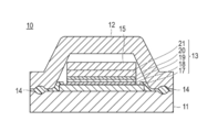
- FIG. 1 is a schematic cross-sectional view of an electronic device 10 according to an embodiment of the present invention. That is, the electronic device 10 shown in FIG. 1 has a base material 11, a sealing member 12, an electronic element body 13 positioned between the base material 11 and the sealing member 12, and a sealing agent composition assembly 14. .
- the protective layer 15 is provided on the top of the electronic element body 13 so as to cover a part of the electronic element body 13.
- the electronic element main body 13 is sealed by joining the base material 11 and the sealing member 12 via the sealant composition assembly 14. That is, the sealing agent composition assembly 14 is disposed at the interface between the base material 11 and the sealing member 12, and the sealing member 12 and the base material 11 are joined by the sealing agent composition assembly 14.
- the base material 11 and the sealing member 12 are firmly joined via the sealing agent composition joined body 14, and can prevent intrusion of oxygen and moisture into the electronic element body.
- the durability of the electronic device can be improved.
- the electronic device 10 has excellent resistance to bending and temperature change.
- FIG. 2 is a schematic cross-sectional view showing the basic configuration of an electronic device according to another embodiment of the present invention.
- the electronic device 10 includes a base material 11, a sealing member 12, an electronic element body 13 positioned between the base material 11 and the sealing member 12, and a sealant composition assembly. 14 and a sealing agent 16 for filling on the electronic element body 13.
- the sealing agent 16 for filling is an arbitrary member provided as necessary.
- the reason why the durability of the electronic device of the present invention is improved is unknown, but as shown in FIGS. 3 and 4, at least one of the metal particles 14 a contained in the applied sealant composition 14 ′. It is considered that when the part melts, the metal particles 14 a aggregate and the metal phase 14 c that binds to the base material 11 and the sealing member 12 is formed, and the sealant composition assembly 14 is formed. It is considered that the base material 11 and the sealing member 12 are firmly joined by the metal phase 14c, and oxygen and moisture can be prevented from entering the electronic element body 13.
- the sealant composition is formed by covering the periphery of the metal phase 14c or the adhesion auxiliary member 30 with the cured resin 14b. It is considered that the object bonded body 14 is formed and the base material 11 and the sealing member 12 are bonded more firmly.
- the present invention is not limited to the above mechanism.
- the electronic element body 13 is an organic EL element body, and includes a first electrode (anode) 17, a hole transport layer 18, a light emitting layer 19, an electron transport layer 20, and a second electrode.
- the electrode (cathode) 21 is formed by being sequentially laminated.
- the electronic device 10 includes an electronic element body 13, a protective layer 15, and a sealing member 12, which are sequentially laminated on a base material 11.
- the electronic device 10 may have a configuration in which the electronic element body 13, the protective layer 15 and the sealing agent 16 for filling, and the base material 11 are sequentially laminated on the sealing member 12. .
- the electronic device 10 is still another It may have a layer.
- the other layer is not particularly limited, and examples thereof include an electrode, a stabilization layer for stabilizing the electronic element body, and a gas absorption layer.
- the base material according to the present invention is not particularly limited. Examples thereof include a glass substrate, metal foil, a gas barrier film having a support and a gas barrier layer.
- the water vapor permeability of the substrate according to the present invention is preferably 5 ⁇ 10 ⁇ 3 g / m 2 ⁇ day or less at 60 ° C. and 90% RH, preferably 5 ⁇ 10 ⁇ 4 g / m 2 ⁇ day or less. More preferably, it is 5 ⁇ 10 ⁇ 5 g / m 2 ⁇ day or less.
- the glass substrate examples include a quartz glass substrate, a borosilicate glass substrate, a soda glass substrate, and a non-alkali glass substrate.
- the metal foil aluminum (Al), gold (Au), silver (Ag), chromium (Cr), iron (Fe), nickel (Ni), cobalt (Co), copper (Cu), indium (In),
- the metal foil include tin (Sn), lead (Pb), titanium (Ti), and alloys thereof.
- gas barrier film suitably used as the substrate will be described below.
- the support is long and can hold a gas barrier layer having a gas barrier property (also simply referred to as “barrier property”) described later, and is formed of the following materials. In particular, it is not limited to these.
- the support examples include, for example, polyacrylate ester, polymethacrylate ester, polyethylene terephthalate (PET), polybutylene terephthalate, polyethylene naphthalate (PEN), polycarbonate (PC), polyarylate, polyvinyl chloride (PVC).
- PET polyethylene terephthalate
- PEN polyethylene naphthalate
- PC polycarbonate
- PVC polyarylate
- PVC polyvinyl chloride
- PE Polyethylene
- PP polypropylene
- COP cycloolefin polymer
- COC cycloolefin copolymer
- TAC triacetate cellulose
- PS nylon
- Ny aromatic polyamide
- Resin films such as polysulfone, polyethersulfone, polyimide, polyetherimide, and heat-resistant transparent film having silsesquioxane having an organic-inorganic hybrid structure as a basic skeleton (for example, Product name Sila-DEC; manufactured by Chisso Corporation, and product name Sylplus (registered trademark); manufactured by Nippon Steel Chemical Co., Ltd.), and resin films formed by laminating two or more layers of the above resin Can do.
- Sila-DEC manufactured by Chisso Corporation
- Sylplus registered trademark
- polyethylene terephthalate (PET), polybutylene terephthalate, polyethylene naphthalate (PEN), polycarbonate (PC), etc. are preferably used, and are cast because of their optical transparency and low birefringence.
- PET polyethylene terephthalate
- PEN polyethylene naphthalate
- PC polycarbonate
- TAC, COC, COP, PC, etc. produced by the above method are preferably used, and silsesquioxane having an organic-inorganic hybrid structure in terms of optical transparency, heat resistance, and adhesion to the gas barrier layer
- a heat-resistant transparent film having a basic skeleton is preferably used.
- the process temperature may exceed 200 ° C. in the array manufacturing process.
- the support temperature will change to the glass transition point.
- the elasticity modulus of a support body will fall rapidly, there exists a concern which a support body may be extended by tension
- a heat-resistant transparent film having polyimide, polyetherimide, or silsesquioxane having an organic / inorganic hybrid structure as a basic skeleton.
- the heat-resistant resin represented by these is non-crystalline, the water absorption rate is larger than that of crystalline PET or PEN, and the dimensional change of the support due to humidity becomes larger, so that the gas barrier layer There is a concern of damaging it.
- these heat-resistant materials are used as a support, by forming a gas barrier layer on both sides, the dimensional change due to moisture absorption / desorption of the support film itself under severe conditions of high temperature and high humidity is suppressed. And damage to the gas barrier layer can be suppressed.
- a heat resistant material is used as a support and a gas barrier layer is formed on both sides.
- the support body containing glass fiber, a cellulose, etc. is also used preferably.
- the thickness of the support is preferably about 5 to 500 ⁇ m, more preferably 25 to 250 ⁇ m.
- the support is preferably transparent.
- transparent support means that the light transmittance of visible light (400 to 700 nm) is 80% or more.
- the support is transparent and the gas barrier layer formed on the support is also transparent, a transparent gas barrier film can be obtained, and thus a transparent substrate such as an organic EL element can be obtained. Because.
- the support using the above-mentioned resins or the like may be an unstretched film or a stretched film.
- the support according to the present invention can be produced by a conventionally known general method.
- an unstretched support that is substantially amorphous and not oriented can be produced by melting a resin as a material with an extruder, extruding it with an annular die or a T-die, and quenching.
- the unstretched support is uniaxially stretched, tenter-type sequential biaxial stretching, tenter-type simultaneous biaxial stretching, tubular simultaneous biaxial stretching, and other known methods, such as the flow (vertical axis) direction of the support, or A stretched support can be produced by stretching in the direction perpendicular to the flow direction of the support (horizontal axis).
- the stretching ratio in this case can be appropriately selected according to the resin as the raw material of the support, but is preferably 2 to 10 times in the vertical axis direction and the horizontal axis direction, respectively. Furthermore, in order to improve the dimensional stability of the substrate in the stretched film, it is preferable to perform relaxation treatment after stretching.
- the surface of the support may be subjected to corona treatment before the gas barrier layer is formed.
- the 10-point average roughness Rz defined by JIS B0601: 2001 is preferably in the range of 1 to 500 nm, more preferably in the range of 5 to 400 nm. Preferably, it is in the range of 300 to 350 nm.
- the center surface average surface roughness (Ra) defined by JIS B0601: 2001 is preferably in the range of 0.5 to 12 nm, and more preferably in the range of 1 to 8 nm.
- the material for the gas barrier layer used in the present invention is not particularly limited, and various inorganic barrier materials can be used.
- inorganic barrier materials include, for example, silicon (Si), aluminum (Al), indium (In), tin (Sn), zinc (Zn), titanium (Ti), copper (Cu), cerium (Ce) and Examples thereof include at least one metal selected from the group consisting of tantalum (Ta) and a metal compound such as an oxide, nitride, carbide, oxynitride, or oxycarbide of the above metal.
- the metal compound include silicon oxide, aluminum oxide, titanium oxide, indium oxide, tin oxide, indium tin oxide (ITO), tantalum oxide, zirconium oxide, niobium oxide, aluminum silicate (SiAlO x ), Boron carbide, tungsten carbide, silicon carbide, oxygen-containing silicon carbide, aluminum nitride, silicon nitride, boron nitride, aluminum oxynitride, silicon oxynitride, boron oxynitride, zirconium boride, titanium boride, and composites thereof
- Inorganic barrier materials such as metal oxides such as metal nitrides, metal carbides, metal oxynitrides, metal oxyborides, diamond-like carbon (DLC), and combinations thereof.
- ITO Indium tin oxide
- silicon oxide aluminum oxide
- silicon nitride silicon oxynitride and combinations thereof are particularly preferred inorganic barrier materials.
- ITO is an example of a special member of ceramic material that can be made conductive by appropriately selecting the respective elemental components.
- the method for forming the gas barrier layer is not particularly limited, and includes, for example, a sputtering method (for example, magnetron cathode sputtering, flat plate magnetron sputtering, two-pole AC flat plate magnetron sputtering, two-pole AC rotary magnetron sputtering), a vapor deposition method (for example, resistance heating).
- a sputtering method for example, magnetron cathode sputtering, flat plate magnetron sputtering, two-pole AC flat plate magnetron sputtering, two-pole AC rotary magnetron sputtering
- a vapor deposition method for example, resistance heating
- Vapor deposition electron beam vapor deposition, ion beam vapor deposition, plasma assisted vapor deposition, etc.
- thermal CVD method catalytic chemical vapor deposition (Cat-CVD), capacitively coupled plasma CVD method (CCP-CVD), photo CVD method, plasma CVD method (PE-CVD), an epitaxial growth method, an atomic layer growth method, a chemical vapor deposition method such as a reactive sputtering method, and the like.
- Cat-CVD catalytic chemical vapor deposition
- CCP-CVD capacitively coupled plasma CVD method
- PE-CVD plasma CVD method
- an epitaxial growth method an atomic layer growth method
- a chemical vapor deposition method such as a reactive sputtering method, and the like.
- the gas barrier layer may include an organic layer containing an organic polymer. That is, the gas barrier layer may be a laminate of an inorganic layer containing the inorganic barrier material and an organic layer.
- the organic layer can be polymerized and required using, for example, an electron beam device, UV light source, discharge device, or other suitable device, for example, by applying an organic monomer or oligomer to the support to form the layer It can be formed by crosslinking according to the above.
- the organic layer can also be formed, for example, by depositing an organic monomer or oligomer capable of flash evaporation and radiation crosslinking and then forming a polymer from the organic monomer or organic oligomer. Coating efficiency can be improved by cooling the support.
- Examples of the method for applying the organic monomer or organic oligomer include roll coating (for example, gravure roll coating), spray coating (for example, electrostatic spray coating), and the like.
- the laminated body of an inorganic layer and an organic layer the laminated body of the international publication 2012/003198, international publication 2011/013341, etc. are mentioned, for example.
- the thickness of each layer may be the same or different.
- the thickness of the inorganic layer is preferably 3 to 1000 nm, more preferably 10 to 300 nm.
- the thickness of the organic layer is preferably 100 nm to 100 ⁇ m, more preferably 1 ⁇ m to 50 ⁇ m.
- a coating liquid containing an inorganic precursor such as polysilazane and tetraethyl orthosilicate (TEOS) is wet-coated on a support and then subjected to a modification treatment by irradiation with vacuum ultraviolet light, etc.
- the gas barrier layer is also formed by metallization techniques such as metal plating on the support and adhesion of the metal foil and the resin support.
- the gas barrier layer is formed by modifying a layer containing polysilazane or is a laminate of an inorganic layer and an organic layer. It is preferable.
- the gas barrier layer may be a single layer or a laminated structure of two or more layers.
- the material of each layer may be the same or different.
- the polysilazane used for forming the gas barrier layer according to the present invention is a polymer having a silicon-nitrogen bond, and SiO 2 , Si 3 N 4 having a bond such as Si—N, Si—H, or N—H, and Ceramic intermediate inorganic polymers such as both intermediate solid solutions SiO x N y .
- the polysilazane according to the present invention preferably has the following structure.
- the polysilazane having the following structure can be ceramicized at a relatively low temperature and modified to silica, and therefore is particularly suitable when a film substrate that is easily damaged under high temperature conditions is used.
- R 1 , R 2 and R 3 each represent a hydrogen atom, an alkyl group, an alkenyl group, a cycloalkyl group, an aryl group, an alkylsilyl group, an alkylamino group or an alkoxy group.
- R 1 , R 2 and R 3 may be the same or different.
- n is an integer
- the polysilazane having the structure represented by the general formula (I) is determined to have a number average molecular weight of 150 to 150,000 g / mol. preferable.
- perhydropolysilazane in which all of R 1 , R 2, and R 3 are hydrogen atoms is particularly preferred from the viewpoint of the denseness of the resulting gas barrier layer.
- Perhydropolysilazane is presumed to have a linear structure and a ring structure centered on 6- and 8-membered rings. Its molecular weight is about 600 to 2000 (polystyrene conversion) in terms of number average molecular weight (Mn), is a liquid or solid substance, and varies depending on the molecular weight.
- Polysilazane is commercially available in the form of a solution dissolved in an organic solvent, and the commercially available product can be used as it is as a coating solution for forming a polysilazane layer.
- Examples of commercially available polysilazane solutions include Aquamica (registered trademark) NN120-10, NN120-20, NAX120-20, NN110, NN310, NN320, NL110A, NL120A, NL120-20, NL150A, and NP110 manufactured by AZ Electronic Materials Co., Ltd. NP140, SP140 and the like.
- the solvent for preparing the coating liquid containing polysilazane (hereinafter also simply referred to as polysilazane-containing coating liquid) is not particularly limited as long as it can dissolve polysilazane, but water and reaction that easily react with polysilazane.
- An organic solvent that does not contain a functional group (for example, a hydroxyl group or an amine group) and is inert to polysilazane is preferable, and an aprotic organic solvent is more preferable.
- an aprotic solvent for example, an aliphatic hydrocarbon such as pentane, hexane, cyclohexane, toluene, xylene, solvesso, and turben, an alicyclic hydrocarbon Hydrocarbon solvents such as aromatic hydrocarbons; Halogen hydrocarbon solvents such as methylene chloride and trichloroethane; Esters such as ethyl acetate and butyl acetate; Ketones such as acetone and methyl ethyl ketone; Aliphatics such as dibutyl ether, dioxane and tetrahydrofuran Examples of ethers such as ether and alicyclic ether include tetrahydrofuran, dibutyl ether, mono- and polyalkylene glycol dialkyl ethers (diglymes), and the like.
- the solvent is selected according to purposes such
- the concentration of polysilazane in the polysilazane-containing coating solution is about 0.2 to 35% by mass, although it varies depending on the film thickness of the target gas barrier layer and the pot life of the coating solution.
- the polysilazane-containing coating solution preferably contains a catalyst together with polysilazane in order to promote modification to silicon oxynitride.
- a basic catalyst is preferable, and in particular, N, N-diethylethanolamine, N, N-dimethylethanolamine, triethanolamine, triethylamine, 3-morpholinopropylamine, N, N, Amine catalysts such as N ′, N′-tetramethyl-1,3-diaminopropane, N, N, N ′, N′-tetramethyl-1,6-diaminohexane, Pt compounds such as Pt acetylacetonate, propion Examples thereof include metal catalysts such as Pd compounds such as acid Pd, Rh compounds such as Rh acetylacetonate, and N-heterocyclic compounds.
- the concentration of the catalyst added at this time is preferably in the range of 0.1 to 10% by mass, more preferably 0.2 to 5% by mass, and still more preferably 0.5 to 2% by mass, based on polysilazane. It is. By setting the addition amount of the catalyst within this range, it is possible to avoid excessive silanol formation due to rapid progress of the reaction, decrease in film density, increase in film defects, and the like.
- the following additives can be used as necessary.
- cellulose ethers, cellulose esters for example, ethyl cellulose, nitrocellulose, cellulose acetate, cellulose acetobutyrate, etc.
- natural resins for example, rubber, rosin resin, etc., synthetic resins
- Aminoplasts especially urea resins, melamine formaldehyde resins, alkyd resins, acrylic resins, polyesters or modified polyesters, epoxides, polyisocyanates or blocked polyisocyanates, polysiloxanes, and the like.
- a conventionally known appropriate wet coating method can be employed as a method of applying the polysilazane-containing coating solution.
- a conventionally known appropriate wet coating method can be employed. Specific examples include spin coating method, die coating method, roll coating method, flow coating method, ink jet method, spray coating method, printing method, dip coating method, casting film forming method, bar coating method, gravure printing method and the like. It is done.
- the coating thickness can be appropriately set according to the purpose.
- the coating thickness is preferably about 10 nm to 10 ⁇ m after drying, more preferably 15 nm to 1 ⁇ m, and even more preferably 20 to 500 nm. If the thickness of the polysilazane layer is 10 nm or more, sufficient barrier properties can be obtained, and if it is 10 ⁇ m or less, stable coating properties can be obtained when forming the polysilazane layer, and high light transmittance can be realized.
- Modification process As a method of the modification treatment, a coating liquid containing polysilazane is applied on a support to form a layer (coating film) containing polysilazane, and then the coating film is irradiated with vacuum ultraviolet rays having a wavelength of 200 nm or less. Is preferred.
- the coating film containing polysilazane is modified in the vacuum ultraviolet irradiation process to have a specific composition of SiO x N y .
- Oxygen concentration during irradiation with vacuum ultraviolet rays (VUV) Oxygen is required for the reaction at the time of ultraviolet irradiation, but since vacuum ultraviolet rays are absorbed by oxygen, the efficiency in the vacuum ultraviolet irradiation process tends to be lowered. Therefore, it is preferable to perform the irradiation with vacuum ultraviolet rays in a state where the oxygen concentration is as low as possible.
- An intermediate layer may be further formed between the support for the gas barrier film and the gas barrier layer.
- the intermediate layer preferably has a function of improving the adhesion between the support surface and the gas barrier layer.
- a commercially available support with an easy-adhesion layer can also be preferably used.
- the intermediate layer may be a smooth layer.
- the smooth layer used in the present invention is provided in order to flatten the rough surface of the support where protrusions and the like are present, or to fill the unevenness and pinholes generated in the gas barrier layer due to the protrusions existing on the support. It is done.
- Such a smooth layer is basically produced by curing a photosensitive material or a thermosetting material.
- the gas barrier film according to the present invention may have a bleed-out preventing layer on the support surface opposite to the surface on which the gas barrier layer is provided.
- a bleed-out prevention layer can be provided.
- the bleed-out prevention layer is used for the purpose of suppressing the phenomenon that, when a film having a smooth layer is heated, unreacted oligomers migrate from the film support to the surface and contaminate the contact surface. It is provided on the opposite surface of the supporting body.
- the bleed-out prevention layer may basically have the same configuration as the smooth layer as long as it has this function.
- An overcoat layer may be provided on the gas barrier layer according to the present invention.
- organic resins such as organic monomers, oligomers, and polymers, and organic-inorganic composite resins using monomers, oligomers, and polymers of siloxane and silsesquioxane having an organic group are preferably used. it can.
- the sealing member 12 has a function of sealing the electronic element body 13 by being bonded to the substrate 11 described above via the sealant composition assembly 14.
- the sealing member 12 is disposed to face the base material 11 with the electronic element body 13 interposed therebetween.
- the sealing member 12 may be the gas barrier film described above. Further, when the sealing member is a gas barrier film, the sealing member 12 and the substrate 11 may have the same configuration or different configurations (materials, layer configurations).
- sealing member 12 in addition to the gas barrier film described above, aluminum (Al), gold (Au), silver (Ag), chromium (Cr), iron (Fe), nickel (Ni), cobalt ( Co foils such as Co), copper (Cu), indium (In), tin (Sn), lead (Pb), titanium (Ti), and alloys thereof may be used.
- the sealing member 12 may be a member composed only of a gas barrier layer having no support in the gas barrier film.
- a gas barrier layer having no support in the gas barrier film.
- Specific examples thereof include metal foil such as aluminum foil and copper foil, and a laminate of an inorganic layer and an organic layer described in the section of the gas barrier film.
- the base material and the sealing member have flexibility.
- “flexibility” refers to a property that is flexible and deforms when a force is applied, but returns to its original shape when the force is removed.
- the prescribed flexural modulus is, for example, 1.0 ⁇ 10 3 to 4.5 ⁇ 10 3 [N / mm 2 ] or less.
- Adhesion auxiliary member At least one of the base material and the sealing member has an adhesion auxiliary member made of metal that assists the adhesion between the base material and the sealing member, abuts on a sealant composition assembly, which will be described later. It is preferable.
- FIG. 4 is a schematic diagram showing the electronic device 10 sealed with the base material 11 having the adhesion assisting member 30 and the sealing member 12.
- the sealant composition 14 ′ forms the metal phase 14c by heating the metal particles 14a, which is one of its components, and melting and aggregating at least a part of the metal particles 14a.
- the sealant composition assembly 14 is formed and exhibits excellent sealing performance.
- the molten metal particles 14a have a very high affinity for metal.
- the base material 11 and / or the sealing member 12 is provided with the adhesion assisting member 30 at a portion to be joined, so that the base material 11 and //
- the sealing member 12 becomes easy to bind to the metal phase 14c formed by melting and aggregating the metal particles 14a in the sealant composition 14 ′, and is formed using the sealant composition 14 ′.
- the material (metal) of the adhesion assisting member 30 preferably has a high affinity with the metal particles 14a included in the sealant composition 14 '.
- metal particles such as Ag—Sn—Cu, Sn—Bi, Sn—In, and Sn—Bi—In are used, Sn, Cu, Ag, Au, Ni, and the like are preferably used.
- Ag Ag, Cu metal nanoparticles, Ag, Cu, Au or the like is preferably used.
- the method for installing the adhesion assisting member 30 on the base material 11 or the sealing member 12 is not particularly limited as long as it is a method capable of placing the metal in close contact with the base material 11 or the sealing member 12. Specifically, for example, physical methods such as vapor deposition, sputtering, etc .; chemical methods such as plating, printing of metal ink containing metal powder, metal nanoparticles, etc., reduction of metal salts, and the like are used.
- the sealant composition assembly according to the present invention includes a metal and a resin including a single metal or an alloy.
- the sealing agent composition which is a raw material for forming the sealing agent composition assembly includes metal particles including a single metal or an alloy and a resin. By melting at least a part of the metal particles contained in the sealant composition, a sealant composition assembly can be formed.
- simple metals or alloys include, for example, indium (In), bismuth (Bi), lead (Pb), tin (Sn), cadmium (Cd), copper (Cu), silver (Ag), and antimony (Sb). , Zinc (Zn), gallium (Ga), germanium (Ge) or the like, or a metal alloy of two or more of the above metals.
- indium, bismuth, tin, silver, or an alloy thereof is preferable. More preferably, it is a metal or metal particle containing tin and at least one of indium and bismuth.
- bismuth is included, it is preferable from the viewpoint of low melting point and low toxicity.
- indium it is preferable from a viewpoint that the ductility and the wettability with respect to the inorganic oxide contained in the said gas barrier layer etc. improve.
- the content of tin is 10 to 60, where the total amount of tin and at least one of indium and bismuth is 100% by mass. Mass% is preferred.
- Particularly preferred alloys include Bi57In26Sn17 (melting point 79 ° C), Bi54In29.7Sn16.3 (melting point 81 ° C), In52.2Sn46Zn1.8 (melting point 108 ° C), Bi67In23Sn10 (melting point 109 ° C), In52Sn48 (melting point 138 ° C). Is mentioned.
- the surface is oxidized and covered with an oxide, which prevents the melting, in the metal particles contained in the sealant composition, It is preferable to use a flux component having a flux characteristic that reduces oxide on the surface and promotes melting.
- the flux component is preferably a carboxylic acid anhydride.
- the carboxylic acid anhydride preferably include at least one compound selected from the compounds represented by the following structural formulas (1) to (5).
- the carboxylic acid anhydrides represented by the structural formulas (1) to (3) have a cyclic structure having an internal strain, and therefore are likely to cause ring opening chemically and thermally.
- the carboxylic acid anhydrides represented by the structural formulas (4) to (5), which are anhydrides, are ester-similar to “— (C ⁇ O) —O— (C ⁇ O) —” which is easily hydrolyzed inside the molecule. Due to the structure, ring opening is likely to occur chemically and thermally. For this reason, these carboxylic acid anhydrides have high reactivity of hydrolysis reaction, and the flux component exhibits an excellent flux action at a low heating temperature.
- the carboxylic acid anhydride is represented by succinic acid anhydride, glutaric acid anhydride, diglycolic acid anhydride, thiodiglycolic acid anhydride, and the following structural formulas (6) to (7). It is also preferable to include at least one compound selected from the group consisting of polymer acid anhydrides.
- succinic anhydride, glutaric anhydride, diglycolic anhydride, and thiodiglycolic anhydride are particularly susceptible to ring opening because the internal strain of the cyclic structure is particularly large, and the structural formula (
- the polymer-type acid anhydrides shown in 6) to (7) also have an ester-like structure of “— (C ⁇ O) —O— (C ⁇ O) —” which is easily hydrolyzed inside the molecule, so that the ring is opened. Is particularly likely to occur. For this reason, these carboxylic acid anhydrides have very high reactivity of hydrolysis reaction, and the flux component exhibits particularly excellent flux action at a low heating temperature.
- the sealant composition may contain a reaction accelerator containing at least one compound selected from the group consisting of a heterocyclic compound having a nitrogen atom, a polyamine compound, and an adduct thereof. preferable.
- the addition amount of the flux component is preferably from 0.1 to 30 parts by weight, more preferably from 1 to 10 parts by weight, based on 100 parts by weight of the whole sealant composition.
- the particle size of the metal particles contained in the sealant composition is not particularly limited, but is preferably 50 ⁇ m or less, and preferably 20 ⁇ m or less from the viewpoint of ease of melting and joining. Moreover, it is preferable that it is 5 micrometers or more at the point which is hard to be influenced by an oxide film, and it is more preferable that it is 10 micrometers or more. From the viewpoint of increasing the packing density of the metal particles in the sealant composition, it is also preferable to mix metal particles having different particle diameters. As the particle size, a value of 50% particle size (median particle size) obtained by a laser diffraction / scattering method is adopted.
- the metal particles may be metal nanoparticles having a particle size of 100 nm or less.
- Metal particles are known to have a lower sintering start temperature (melting point) by reducing the particle size. From the viewpoint that additives such as flux components are not required for silver, gold, etc., which are difficult to oxidize.
- metal nanoparticles can be preferably used.
- the type of metal in the case of metal nanoparticles is not particularly limited, but gold, silver, copper, platinum, and a silver-copper alloy are preferable from the viewpoints of ease of manufacture and stability.
- the amine compound may be deposited on the surface of the metal nanoparticles. Since the amine compound attached to the metal nanoparticles forms a protective film on the surface of the metal nanoparticles, after a certain number of metal atoms gather to form the metal nanoparticles, the amine protective film further increases the It is thought that it becomes difficult for metal atoms to bond. For this reason, it is considered that metal nanoparticles having a uniform particle diameter can be obtained stably.
- Examples of the amine compound include ethylenediamine, N, N-dimethylethylenediamine, N, N′-dimethylethylenediamine, N, N-diethylethylenediamine, N, N′-diethylethylenediamine, 1,3-propanediamine, 2,2 -Dimethyl-1,3-propanediamine, N, N-dimethyl-1,3-diaminopropane, N, N'-dimethyl-1,3-diaminopropane, N, N-diethyl-1,3-diaminopropane, 1,4-diaminobutane, 1,5-diamino-2-methylpentane, 1,6-diaminohexane, N, N′-dimethyl-1,6-diaminohexane, 1,7-diaminoheptane, 1,8- Diaminooctane, 2-ethoxyethylamine, dipropylamine,
- a metal oxalate and an amine compound are reacted to form a complex compound, and then the complex compound is heated in a range of 100 to 200 ° C.
- the method of carrying out low temperature thermal decomposition is mentioned.
- the particle size of the metal nanoparticles is not particularly limited, but is preferably 50 nm or less, and preferably 20 nm or less, from the viewpoint of ease of melting and joining.
- the lower limit is not particularly limited, but is preferably 5 nm or more, and more preferably 10 nm or more. From the viewpoint of increasing the packing density of metal particles, it is also preferable to mix particles having different particle sizes.
- the particle diameter (median particle diameter) observed with the scanning electron microscope shall be employ
- the shape of the metal particles is not particularly limited, and examples thereof include a polyhedron shape, a regular polyhedron shape, a spherical shape, a spheroid shape, a scale shape, a disk shape, a dendritic shape, and a fibrous shape. From the viewpoint of the viscosity of the resin / metal particle mixture and the surface area per volume of the metal particles being small, it is preferably spherical.
- the melting point of the metal particles is not particularly limited, but is preferably from 80 to 200 ° C., more preferably from 100 to 160 ° C., and from 110 to 140 ° C. from the viewpoints of ease of manufacturing an electronic device and thermal stability. More preferably.
- the content of the metal particles in the sealant composition is preferably 50 to 90 parts by weight, more preferably 60 to 85 parts by weight, with the total amount of the sealant composition being 100 parts by weight. preferable.
- the metal particles may be used alone or in combination of two or more.
- the resin contained in the encapsulant composition assembly and the encapsulant composition is not particularly limited, and examples thereof include thermoplastic resins, thermosetting resins, and photocurable resins.
- a curable resin the resin contained in the encapsulant composition is in an uncured state, and the resin contained in the encapsulant composition assembly is in a cured state.
- More specific examples include, for example, epoxy resins, acrylic resins, polyolefin resins, fluororesins, polyvinylidene chloride resins, ionomer resins, urethane resins, ethylene-vinyl acetate copolymer resins, polyimide resins, cyanate ester resins, Examples include benzoxazine resin. Especially, it is more preferable that at least one of an epoxy resin and an acrylic resin is included.
- the sealant composition (mixture of components other than metal particles such as the resin and the flux component) when the metal particles are removed from the sealant composition
- the viscosity after standing for 1 minute at the melting point of the metal particles contained in the substrate is preferably 1 Pa ⁇ s or less, and more preferably 100 mPa ⁇ s or less.
- the melting point known from the composition of the alloy is used here as the melting point of the encapsulated metal particles. When the melting point from the solid phase and the melting point from the liquid phase are different as in an alloy, the average is taken as the melting point.
- the melting point of the metal contained is the weight average value of the melting points of the metal particles.
- the value measured with the E-type viscosity meter shall be employ
- these resins may be used alone or in combination of two or more kinds, and commercially available products or synthetic products may be used.
- the content of the resin in the sealant composition assembly or the sealant composition is 5 to 50 parts by weight based on 100 parts by weight of the total amount of the sealant composition assembly or the sealant composition. It is preferably 10 to 20 parts by weight.
- the sealing agent composition may include a curing agent for the resin.
- a curing agent for the resin There is no restriction
- Monoaldehydes such as formaldehyde, acetaldehyde, propionaldehyde, butyraldehyde; amino-formaldehyde resins such as methylol urea, methylol melamine, alkylated methylol urea, alkylated methylolated melamine, acetoguanamine, condensates of benzoguanamine and formaldehyde;
- salts of divalent to tetravalent metals such as sodium, potassium, magnesium, calcium, aluminum, iron, nickel, zirconium and oxides thereof can be mentioned.
- These curing agents may be used alone or in combination of two or more.
- the content of the curing agent in the sealant composition is preferably 1 to 10 parts by weight, with the total amount of the sealant composition being 100 parts by weight.
- the sealant composition may contain other additives as necessary.
- other additives include, for example, triphenylsulfonium hexafluoroantimonate, triphenylsulfonium phosphate, p- (phenylthio) phenyldiphenylsulfonium hexafluoroantimonate, 4-chlorophenyldiphenylsulfonium hexafluorophosphate, bis [ 4- (diphenylsulfonio) phenyl] sulfide bishexafluorophosphate, bis [4- (diphenylsulfonio) phenyl] sulfide bishexafluoroantimonate, diallyl iodonium hexafluoroantimonate, diethoxyacetophenone, 4- ( 2-hydroxyethoxy) phenyl- (2-hydroxy-2-propyl) ketone, 2-methyl-2-morpholino (4-thiomethylpheny
- the sealant composition which is a raw material for bonding the sealant composition, is cured by external energy to form a sealant composition assembly.
- the curing method is not particularly limited, and examples thereof include heating, ultraviolet irradiation, electron beam irradiation, and laser irradiation.
- the arrangement of the encapsulant composition assembly and the encapsulant composition that is a raw material thereof is not particularly limited, but is preferably arranged outside the electronic element body 13 as shown in FIGS.
- the effects of the present invention can be obtained more efficiently by arranging the sealant composition assembly and the sealant composition that is a raw material thereof.
- a commercially available product or a synthetic product (prepared product) may be used as the sealant composition that is a raw material of the sealant composition assembly.
- the sealant composition for example, there is a method in which the metal particles, resin, and other components as described above are stirred and mixed at ⁇ 20 to 40 ° C. for 1 to 24 hours. Applied.
- the viscosity at 25 ° C. before curing of the sealant composition which is a raw material of the sealant composition assembly according to the present invention, is preferably 100 to 1000 Pa ⁇ s. If it is this range, it can apply
- the value measured with the E-type viscosity meter shall be employ
- the electronic element body is the body of the electronic device. 1 to 4, the electronic element body is an organic EL element body.
- the electronic element body of the present invention is not limited to such a form, and a known electronic device body to which sealing by a gas barrier film can be applied can be used.
- a solar cell (PV), a liquid crystal display element (LCD), electronic paper, a thin film transistor, a touch panel, and the like can be given.
- PV solar cell
- LCD liquid crystal display element
- electronic paper a thin film transistor, a touch panel, and the like
- the electronic element body (organic EL element body) 13 includes a first electrode (anode) 17, a hole transport layer 18, a light emitting layer 19, an electron transport layer 20, and a second electrode (cathode). ) 21 etc.
- a hole injection layer may be provided between the first electrode 17 and the hole transport layer 18, or an electron injection layer may be provided between the electron transport layer 20 and the second electrode 21. May be provided.
- the hole injection layer, the hole transport layer 18, the electron transport layer 20, and the electron injection layer are arbitrary layers provided as necessary.
- an organic EL element will be described as an example of a specific electronic device configuration.
- First electrode anode
- an electrode material made of a metal, an alloy, an electrically conductive compound or a mixture thereof having a high work function (4 eV or more) is preferably used.
- a hole injection layer (anode buffer layer) may be present between the first electrode (anode) and the light emitting layer or the hole transport layer.
- the hole injection layer is a layer provided between the electrode and the organic layer in order to lower the driving voltage and improve the light emission luminance.
- the hole transport layer is made of a hole transport material having a function of transporting holes, and in a broad sense, a hole injection layer and an electron blocking layer are also included in the hole transport layer.
- the hole transport layer can be provided as a single layer or a plurality of layers.
- the light emitting layer refers to a blue light emitting layer, a green light emitting layer, and a red light emitting layer.
- the light emitting layer refers to a blue light emitting layer, a green light emitting layer, and a red light emitting layer.
- the electron transport layer is made of a material having a function of transporting electrons and is included in the electron transport layer in a broad sense.
- An electron injection layer is a layer provided between an electrode and an organic layer in order to reduce drive voltage and improve light emission luminance.
- the electron injection layer (cathode buffer layer) formed in the electron injection layer forming step is made of a material having a function of transporting electrons and is included in the electron transport layer in a broad sense.
- An electron injection layer is a layer provided between an electrode and an organic layer in order to reduce drive voltage and improve light emission luminance.
- the second electrode As the second electrode (cathode), a material having a small work function (4 eV or less) metal (referred to as an electron injecting metal), an alloy, an electrically conductive compound, and a mixture thereof is used.
- an electron injecting metal a material having a small work function (4 eV or less) metal
- an alloy a material having a small work function (4 eV or less) metal
- an alloy a material having a small work function (4 eV or less) metal
- an electrically conductive compound As the second electrode (cathode), a material having a small work function (4 eV or less) metal (referred to as an electron injecting metal), an alloy, an electrically conductive compound, and a mixture thereof is used.
- the electronic device of the present invention may have a protective layer on the electronic element body as necessary.
- the protective layer has a function of preventing deterioration of the electronic device body such as moisture and oxygen from entering the device, a function of insulating the electronic device body disposed on the substrate 11, or the like. It has a function to eliminate the level difference caused by the electronic element body.
- the protective layer may be a single layer or a plurality of layers may be stacked. In this invention, it is preferable that the sealing compound composition and the electronic device are insulated by the protective layer.
- the manufacturing method of the electronic device 10 of the present invention is not particularly limited, and conventionally known knowledge can be referred to as appropriate.
- an electronic element main body is arrange
- the layers constituting the electronic element body for example, the first electrode layer, the hole injection layer, the hole transport layer, the light emitting layer, the electron transport layer, the electron injection layer, the second electrode layer, etc. in order. It is formed by laminating. These forming methods are not particularly limited, and can be produced by appropriately referring to known methods.
- a protective layer is formed as necessary.
- the method for forming the protective layer is not particularly limited, and can be manufactured by appropriately referring to known methods.
- Examples of the method for applying the sealant composition include a micro gravure coating method, a gravure coating method, a bar coating method, a wire bar coating method, a roll coating method, a dip coating method, a flexographic printing method, an offset printing method, and a screen printing method.
- Etc. A liquid crystal dropping method (ODF, One Drop Filling) in which a liquid sealant composition is applied with a dispenser is preferably used because of the ease of controlling the amount of sealant.
- the sealing material for filling is placed inside the sealing agent composition (see reference numeral 14 'in FIGS. 3 and 4), which is a raw material for forming the sealing agent composition connector 14.
- a stop agent 16 is applied. As shown in FIG. 2, it may be applied to the upper surface of the electronic element body 13, or when the protective layer 15 is provided, may be applied to the upper surface of the protective layer 15, or a part of the electronic element body 13 or You may form on the upper surface of all the structure layers.
- sealing agent for fill examples include sealing agents containing epoxy resin, acrylic resin, polyolefin resin, fluororesin, polyvinylidene chloride resin and the like.
- the fill sealant may include a curing agent. These resins may be used alone or in combination of two or more.
- FIG. As shown in (4) to (4), at least a part of the metal particles 14a in the sealant composition 14 ′ is melted and aggregated to form the metal phase 14c bound to the base material 11 and the sealing member 12.
- the method for melting the metal particles is not particularly limited, and examples thereof include heating.
- the heating temperature for melting the metal particles by heating is not particularly limited, but is preferably 100 to 200 ° C.
- the heating time is preferably 1 minute to 30 minutes.
- Step of curing resin in sealant composition step of forming sealant composition assembly
- the resin 14b in the sealant composition 14 ′ is cured.
- a sealant composition assembly 14 is formed, and the base material 11 and the sealing member 12 are joined via the sealant composition assembly 14 to seal the electronic element body 13.
- the electronic device 10 is formed.
- the method for curing the resin 14b in the sealant composition 14 ' is not particularly limited, and examples thereof include heating, ultraviolet irradiation, electron beam irradiation, and laser irradiation.
- this process may serve as the process of said (4). That is, the step (4) and this step may be performed by one heating or laser irradiation.
- thermoplastic resin support a 125 ⁇ m thick polyethylene naphthalate film (Q65FWA, manufactured by Teijin DuPont Films Ltd.) with easy adhesion processing on both sides was used. As shown below, a bleed-out prevention layer was opposite on one side. What formed the smooth layer in the surface was made into the support body (a).
- a UV curable organic / inorganic hybrid hard coat material OPSTAR (registered trademark) Z7535 manufactured by JSR Corporation is applied to one surface side of the thermoplastic resin support under the condition that the film thickness after drying is 4.0 ⁇ m. Then, as a curing condition, a high pressure mercury lamp was used in an air atmosphere with an irradiation energy amount of 1 J / cm 2 , and a curing process was performed at 80 ° C. for 3 minutes to form a bleedout prevention layer.
- the UV curable organic / inorganic hybrid hard coat material OPSTAR (registered trademark) Z7501 manufactured by JSR Corporation is dried on the surface of the thermoplastic resin support opposite to the surface on which the bleed-out prevention layer is formed. After coating under the condition that the film thickness is 4.0 ⁇ m after that, the film is dried at 80 ° C. for 3 minutes, and then irradiated with an irradiation energy of 1 J / cm 2 as a curing condition using a high-pressure mercury lamp in an air atmosphere. And cured to form a smooth layer.
- OPSTAR registered trademark
- Z7501 manufactured by JSR Corporation
- the surface roughness Ra measured in accordance with the method defined in JIS B 0601: 2001 of the obtained smooth layer was 1 nm.
- Rz was 20 nm.
- the coated surface of the smooth layer was the surface of the anchor coat layer.
- the surface roughness was measured using an AFM (Atomic Force Microscope) SPI3800N DFM manufactured by SII.
- the measurement range at one time is 80 ⁇ m ⁇ 80 ⁇ m, the measurement location is changed and the measurement is performed three times, and the Ra value obtained by each measurement and the average of the 10-point average roughness Rz are measured. Value.
- a coating solution containing the following polysilazane (polysilazane-containing coating solution 1) is applied using a spin coater so that the film thickness after drying becomes 150 nm at a coating speed of 30 m / min. It was applied with.
- the drying conditions were 100 ° C. and 2 minutes.
- the polysilazane-containing coating solution 1 is applied in the same manner onto the polysilazane layer 1 obtained above, vacuum ultraviolet irradiation (irradiation amount: 1700 mJ / cm 2 ) is performed, and the dry film thickness is 50 nm on the polysilazane layer 1.
- a gas barrier layer 1 on which a certain polysilazane layer 2 was laminated was formed on a smooth layer.
- the composition of the gas barrier layer 1 is SiON, and the thickness of the gas barrier layer 1 (the total thickness of the polysilazane layer 1 and the polysilazane layer 2). was 200 nm.
- WVTR water vapor permeability
- the conveyance speed was 0.5 m / min.
- the thickness of the thin film layer in the obtained laminated film was 0.3 ⁇ m.
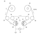
- the manufacturing apparatus 31 shown in FIG. 5 includes a feed roller 32, transport rollers 33, 34, 35, and 36, film forming rollers 39 and 40, a gas supply pipe 41, a plasma generation power source 42, and a generator. Magnetic field generators 43 and 44 installed inside the film rollers 39 and 40 and a winding roller 45 are provided.
- film forming rollers 39 and 40, a gas supply pipe 41, a plasma generation power source 42, and magnetic field generation apparatuses 43 and 44 are disposed in a vacuum chamber (not shown). Further, in the manufacturing apparatus 31, the vacuum chamber is connected to a vacuum pump (not shown), and a vacuum pump that can adjust the pressure in the vacuum chamber is used.
- a vacuum pump not shown
- a film forming gas (raw material gas or the like) is supplied into the vacuum chamber under the film forming conditions of the laminated film 1 described above, while a pair of film forming rollers (film forming rollers). 39 and 40), the film-forming gas (raw material gas or the like) is decomposed by plasma, and a support (on the surface of the substrate 2 on the film-forming roller 39 and on the film-forming roller 40) is generated.
- a laminated film 1 was produced in which an inorganic layer 3 made of oxygen-containing silicon carbide was formed on the surface of 2 by a plasma CVD method.
- the atomic ratio at each distance from the film surface of the laminated film was confirmed by elemental composition analysis in the depth direction using an X-ray photoelectron spectroscopy (XPS) device (Quanta SXM, manufactured by ULVAC-PHI). It has an extreme value, and it was confirmed that the difference between the maximum and minimum carbon concentration was 7 at%.
- XPS X-ray photoelectron spectroscopy
- the polysilazane-containing coating solution 1 is coated on the inorganic layer obtained above in the same manner as the gas barrier film 1 and is irradiated with vacuum ultraviolet rays (irradiation amount: 2000 mJ / cm 2 ), on the layer made of oxygen-containing silicon carbide.
- thermoplastic resin support a 125 ⁇ m-thick polyethylene naphthalate film (Q65FWA, manufactured by Teijin DuPont Films, Ltd.) that was easily bonded on both sides was used as the support (I).
- gas barrier film 4 instead of the gas barrier layer 3, three barrier films (SiO 2 film having a thickness of 30 nm) produced by the same method as described in Example E2 of WO 2011/013341 were bonded together, and the organic layer and A gas barrier film 4 was produced in the same manner as the gas barrier film 3 except that the gas barrier layer 4 on which an inorganic layer was laminated was produced.
- solder particles were produced according to a conventional method.
- the produced solder particles had an average particle size of 15 ⁇ m and a melting point of 138 ° C.
- solder particles were produced according to a conventional method.
- the produced solder particles had an average particle size of 15 ⁇ m and a melting point of 118 ° C.
- ⁇ Sealing agent composition DT-4> 5.35 g (20 mmol) of oleylamine, 2.02 g (20 mmol) of hexylamine and 5 ml of methanol were mixed, 1.519 g (5 mmol) of silver oxalate was added to this mixed solution, and 1 ml of water was further added at room temperature. The mixture was stirred for 2 hours to dissolve the silver oxalate. The product obtained at this time was confirmed to be a complex compound containing silver, oxalate ion, oleylamine and hexylamine by analysis using FT-IR.
- NP-A was composed of spherical monodispersed ultrafine particles having a particle size of 12.5 nm.
- the yield as silver was 87.8%.
- the weight ratio of Ag was 90%.
- NP-A 85 parts by weight of NP-A obtained above, 11 parts by weight of liquid epoxy resin (manufactured by Nippon Steel Chemical Co., Ltd., YD128), and curing agent (manufactured by Ajinomoto Fine Techno Co., Ltd., Amicure (registered trademark) PN-23) 2 parts by weight were uniformly mixed using a disper (mixing temperature 25 ° C., mixing time 1 hour) to obtain a sealant composition DT-4.
- the viscosity of DT-4 measured with an E-type viscometer was 300 Pa (25 ° C.).
- the viscosity of the mixture other than the metal particles after standing at 115 ° C. for 1 minute was 100 mPa ⁇ s.
- ⁇ Fill sealant FT-1 11 parts by weight of a liquid epoxy resin (manufactured by Nippon Steel Chemical Co., Ltd., YD128) and 2 parts by weight of a curing agent (manufactured by Ajinomoto Fine Techno Co., Ltd., Amicure (registered trademark) PN-23) are uniformly mixed using a disper. (Mixing temperature 25 ° C., mixing time 1 hour) to obtain a sealant composition FT-1.
- the viscosity of FT-1 measured with an E-type viscometer was 750 mPa (25 ° C.).
- the organic EL element which is an organic thin film electronic device was produced in the following procedures using 0.7 mm-thick alkali-free glass as a base material.
- ITO indium tin oxide
- the hole transport layer forming coating solution shown below was applied by an extrusion coater so that the thickness after drying was 50 nm, and then dried to form a hole transport layer. Formed.
- the cleaning surface modification treatment of the gas barrier film was performed using a low pressure mercury lamp with a wavelength of 184.9 nm at an irradiation intensity of 15 mW / cm 2 and a distance of 10 mm.
- the charge removal treatment was performed using a static eliminator with weak X-rays.
- ⁇ Application conditions> The coating process was performed in an atmosphere of 25 ° C. and a relative humidity of 50% RH.
- ⁇ Drying and heat treatment conditions> After applying the hole transport layer forming coating solution, the solvent was removed by applying hot air at a height of 100 mm toward the film formation surface, a discharge air speed of 1 m / s, a width of 5% of the wide air speed, and a temperature of 100 ° C. Subsequently, a back surface heat transfer type heat treatment was performed at a temperature of 150 ° C. using a heat treatment apparatus to form a hole transport layer.
- ⁇ White luminescent layer forming coating solution 1.0 g of host material HA, 100 mg of dopant material DA, 0.2 mg of dopant material DB, and 0.2 mg of dopant material DC are dissolved in 100 g of toluene as a coating solution for forming a white light emitting layer. Got ready.
- the chemical structures of the host material HA, the dopant material DA, the dopant material DB, and the dopant material DC are as shown in the following chemical formula.
- the coating process was performed in an atmosphere having a nitrogen gas concentration of 99% or more, a coating temperature of 25 ° C., and a coating speed of 1 m / min.
- the coating process was performed in an atmosphere having a nitrogen gas concentration of 99% or more, the coating temperature of the electron transport layer forming coating solution was 25 ° C., and the coating speed was 1 m / min.
- an electron injection layer was formed on the electron transport layer formed above.
- the substrate was put into a decompression chamber and decompressed to 5 ⁇ 10 ⁇ 4 Pa.
- cesium fluoride prepared in a tantalum vapor deposition boat was heated in a vacuum chamber to form an electron injection layer having a thickness of 3 nm.
- a mask pattern is formed by vapor deposition using aluminum as a second electrode forming material under a vacuum of 5 ⁇ 10 ⁇ 4 Pa and having an extraction electrode.
- a second electrode having a thickness of 100 nm was stacked.
- SiO 2 was laminated with a thickness of 200 nm by a CVD method, except for a portion to be the extraction portion of the first electrode and the second electrode, and a protective layer was formed on the second electrode layer.
- a sealing member As shown in FIG. 4, as a sealing member (reference numeral 12), a polyethylene terephthalate (PET) film (12 ⁇ m thickness) is applied to a 30 ⁇ m-thick aluminum foil (manufactured by Toyo Aluminum Co., Ltd.) and an adhesive (2 What was dry-laminated using a liquid reaction type urethane adhesive) (adhesive layer thickness 1.5 ⁇ m) was prepared. Furthermore, a width of 0.5 mm and a thickness as an adhesion protection member (reference numeral 30) are provided on the base material (reference numeral 11) and on the sealing member (reference numeral 12) in contact with the sealing agent composition (reference numeral 14 '). Copper was deposited by a vacuum deposition method with a thickness of 50 nm.
- the encapsulant composition DT-2 (symbol 14 ′) is applied to the copper (symbol 30) portion of the aluminum foil of the sealing member (symbol 12) by using an ODF method using a dispenser manufactured by Musashi Engineering Co., Ltd. Set up.
- the sealing agent FT-1 for fill (reference numeral 16) was dropped into the sealing agent composition DT-2 (reference numeral 14 ') at 10 ⁇ 10 portions at equal intervals.
- a vacuum bonding apparatus manufactured by Run Technical Service Co., Ltd.
- the electronic element body (reference numeral 13) on which the protective layer (reference numeral 15) is formed is bonded, heated at 160 ° C. for 5 minutes, and solder particles (symbol 14a) of the sealant composition DT-2 (reference numeral 14 ′).
- solder particles (symbol 14a) of the sealant composition DT-2 reference numeral 14 ′.
- a thermosetting liquid epoxy resin reference numeral 14b in the upper diagram of FIG. 4
- an epoxy resin (reference numeral 14b in the lower diagram of FIG. 4). ) was formed to complete the sealing, and an organic EL element 102 as an electronic device (reference numeral 10) was obtained.
- Examples 2 to 11, Comparative Examples 1 to 4 The organic EL elements 101 and 103 to 115 were prepared in the same manner as in Example 1 except that the base material, sealing member, sealant composition, and fill sealant shown in Table 1 below were used. Produced.
- Example 12 After using the gas barrier film 2 and producing the electron injection layer in the same manner as in Example 1, a transparent organic EL lighting element was produced as follows.
- ITO having a thickness of 150 nm was formed by sputtering under a vacuum of 5 ⁇ 10 ⁇ 4 Pa, and a mask pattern was formed so that the light emitting portion was 4 cm ⁇ 4 cm.
- SiO 2 was laminated with a thickness of 200 nm by a CVD method, except for the portions to be taken out of the first electrode layer and the second electrode layer, and a protective layer was formed on the second electrode layer.
- solder particles were produced according to a conventional method.
- the produced solder particles had an average particle size of 15 microns and a melting point of 118 ° C.
- ⁇ Fill sealant FT-2> Disperser 25 parts by weight of liquid epoxy resin (manufactured by Nippon Steel Chemical Co., Ltd., YD128), 25 parts by weight of 1,6-bis (2,3-epoxypropoxy) naphthalene and 50 parts by weight of tetrahydromethylphthalic anhydride Were mixed uniformly to prepare a sealant FT-2 for fill.
- the gas barrier film 2 having excellent ultraviolet transparency is used as the sealing member (reference numeral 12) (because the UV curable sealing agent composition DU-1 is cured by ultraviolet irradiation),
- the sealant composition DU-1 (symbol 14 ′) was applied by an ODF method using a dispenser manufactured by Musashi Engineering Co., Ltd.
- Sealing agent FT-2 for fill (reference numeral 16) was dropped into the sealing agent composition DU-1 (reference numeral 14 ') at 10 ⁇ 10 portions at equal intervals.
- this sealing member (reference numeral 12), a vacuum bonding apparatus manufactured by Run Technical Service Co., Ltd., so that the thickness of the sealing agent layer (the coating film of the sealing agent composition DU-1) is 20 ⁇ m. Then, it was bonded to the electronic element body (reference numeral 13) on which the protective layer (reference numeral 15) was formed.
- continuous wave Nd YAG laser light (wavelength: 1064 nm, frequency: 1000 Hz, output: 17 W) is set to a laser beam convergence angle of 2.5 ° at the focal point of the laser light.
- the diameter of the light beam (beam diameter) was set to 300 ⁇ m, and the encapsulant composition DU-1 (symbol 14 ′) was irradiated with laser while moving at a laser scanning speed of 15 mm / sec. Thereafter, a 395 nm semiconductor laser was irradiated with a spot diameter of 2 mm.
- A The element deterioration resistance rate is 90% or more.
- B The element deterioration resistance ratio is 60% or more and less than 90%.
- ⁇ The element deterioration resistance ratio is 20% or more and less than 60%. The deterioration resistance rate is less than 20%.
- the electronic devices 102 to 104, 107 to 111, 113 to 115, and 201 (Examples 1 to 12) of the present invention are the electronic devices of Comparative Examples 1 to 4.
- the device is excellent in device deterioration resistance after deterioration treatment (durability test is not performed), and is further excellent in device deterioration resistance (durability) when subjected to deterioration treatment after various durability tests.
- the element deterioration resistance (durability) after the bending test, after the thermal cycle (1) and after the thermal cycle (2) is excellent as a durability test.
- the thermal history of the electronic device can be reduced by performing the UV curing treatment of the sealant composition.
- an indium tin oxide (ITO) transparent conductive film deposited as a first electrode (anode) with a thickness of 150 nm (sheet resistance 12 ⁇ / square) is used as a normal photo.
- a first electrode was formed by patterning to a width of 10 mm using a lithography method and wet etching. The patterned first electrode was cleaned in the order of ultrasonic cleaning with a surfactant and ultrapure water, followed by ultrasonic cleaning with ultrapure water, dried by nitrogen blowing, and finally subjected to ultraviolet ozone cleaning.
- PEDOT-PSS (CLEVIOS (registered trademark) PVP AI 4083, manufactured by Helios Co., Ltd., conductivity: 1 ⁇ 10 ⁇ 3 S / cm) made of a conductive polymer and a polyanion is used as a hole transport layer.
- An isopropanol solution containing 0% by mass was prepared, and the substrate was applied and dried using a blade coater whose temperature was adjusted to 65 ° C. so that the dry film thickness was about 30 nm. Then, it heat-processed with the warm air of 120 degreeC for 20 second, and formed the positive hole transport layer on said 1st electrode. From then on, it was brought into the glove box and worked under a nitrogen atmosphere.
- the element formed up to the hole transport layer was heated at 120 ° C. for 3 minutes in a nitrogen atmosphere.
- This solution was applied and dried using a blade coater whose temperature was adjusted to 65 ° C. so that the dry film thickness was about 5 nm. Thereafter, heat treatment was performed for 2 minutes with warm air at 100 ° C. to form an electron transport layer on the photoelectric conversion layer.
- the element on which the electron transport layer was formed was placed in a vacuum deposition apparatus. Then, after setting the element so that the shadow mask with a width of 10 mm is orthogonal to the transparent electrode, the inside of the vacuum deposition apparatus is depressurized to 10 ⁇ 3 Pa or less, and then silver is deposited to 100 nm at a deposition rate of 2 nm / second, A second electrode (cathode) was formed on the electron transport layer.
- a sealing member (reference numeral 12)
- a polyethylene terephthalate (PET) film (12 ⁇ m thickness) is applied to a 30 ⁇ m thick aluminum foil (manufactured by Toyo Aluminum Co., Ltd.) and an adhesive (2 What was dry-laminated using a liquid reaction type urethane adhesive) (adhesive layer thickness 1.5 ⁇ m) was prepared.
- the sealant composition DT-3 (symbol 14 ') was applied by an ODF method using a dispenser manufactured by Musashi Engineering Co., Ltd.
- Sealant FT-1 for fill (reference numeral 16) was dropped into the sealant composition DT-3 (reference numeral 14 ') at 10 ⁇ 10 portions at equal intervals.
- this sealing member reference numeral 12
- a vacuum bonding apparatus manufactured by Run Technical Service Co., Ltd., so that the thickness of the sealing agent layer (the coating film of the sealing agent composition DT-3) is 20 ⁇ m.
- the electronic element body (reference numeral 13) on which the protective layer (reference numeral 15) is formed is bonded, heated at 160 ° C. for 5 minutes, and solder particles (reference numeral 14a) of the sealant composition DT-3 (reference numeral 14 ′).
- Sample A before the durability test Sample B subjected to the bending test in the same manner as the above (Evaluation of black spot: Durability test Bending test) and (Evaluation of the black spot: Durability test Thermal cycle) and Sample subjected to the thermal cycle C was left as an accelerated deterioration treatment in an environment of 60 ° C. and 90% RH for 1000 hr, and the open circuit voltage, the fill factor, and the photoelectric conversion efficiency were evaluated.
- the sample A before the durability test refers to a sample in which neither the accelerated deterioration treatment nor the durability test is performed for the organic photoelectric conversion element 301.
- Sample B subjected to the bending test is 100 times as an durability test (bending test) for the organic photoelectric conversion element 301, which is wound on a cylinder having a diameter of 10 cm, left for 5 minutes, then spread on a plane and left for 5 minutes.
- Sample C subjected to thermal cycling refers to a sample obtained by performing 500 cycles of ⁇ 40 ° C. to 85 ° C. as a durability test (thermal cycle) on the organic photoelectric conversion element 301.
- the organic photoelectric conversion element 301 of Example 13 did not show performance deterioration in durability evaluation, and good sealing performance was obtained. That is, the short-circuit current density before the accelerated deterioration treatment between the sample A before the durability test, the sample B after the durability test (bending test), and the sample C after the durability test (thermal cycle) is opened. There was no significant difference in voltage, fill factor and photoelectric conversion efficiency. Similarly, no significant difference was observed between the sample A and the samples B and C in the short-circuit current density, the open-circuit voltage, the fill factor, and the photoelectric conversion efficiency after the accelerated deterioration treatment.
Landscapes
- Physics & Mathematics (AREA)
- Optics & Photonics (AREA)
- Engineering & Computer Science (AREA)
- Manufacturing & Machinery (AREA)
- Electroluminescent Light Sources (AREA)
Description
本発明は、電子デバイスおよびその製造方法に関する。
有機エレクトロルミネッセンス素子(有機EL素子)、有機太陽電池、有機トランジスタ、無機エレクトロルミネッセンス素子、無機太陽電池(例えばCIGS太陽電池)等の電子デバイスは、使用環境中に存在する酸素および水分に敏感である。このため、電子デバイスを酸素および水分から保護するための、封止方法が数多く提案されており、ガラスまたは金属を用いたバリア性基材を使って封止する方法が実用化されている。
これらの基材の封止方法としては、基材と電子素子本体が搭載された封止基板とを溶接する方法が考えられるが、電子デバイスの耐熱性の問題等から実用化できていない。このため、通常は有機化合物からなる接着剤を用いた封止方法が使われている。しかし、かかる接着剤による封止方法では、接着剤部からの水分、酸素の侵入が課題であった。これに対して、レーザー光等を使って局部的に融着する方法が検討されている(例えば、特許文献1,2参照)。しかしながら、熱膨張係数の異なる異種の材料や、大型の電子デバイスでは接合できない、接合強度が十分でない等の課題がある。
一方、近年、電子デバイスの普及に伴い、軽量化、屈曲性、割れ防止による可搬性の向上、曲面への追従性による設置場所の拡大、ロール・ツー・ロール方式の生産による生産コストの低減が望まれている。このため、基材として、従来のガラスに代えて、厚さ100μm以下の薄膜のガラスや、可撓性の樹脂基材にガスバリア層を設置してなるガスバリア性フィルムを用いた電子デバイスが提案されている(例えば、特許文献3参照)。
このような可撓性の樹脂基材を使用した電子デバイスでは、封止部においても高い可撓性と高い封止性能とが求められているが、これらの課題を満足する手段が見いだせていなかった。
一方、特許文献4および5では、低融点金属を溶融させて封止する方法が開示されており、特許文献6では、金属微粒子を高速で吹き付けて金属膜を形成し、この金属膜により封止する方法が開示されている。
しかしながら、特許文献4~6に記載の技術では、電子デバイスの屈曲時や温度変化時に、封止性能が低下するという問題があった。
そこで本発明は、屈曲や温度変化に対する耐性に優れ、耐久性に優れる電子デバイスおよびその製造方法を提供することを目的とする。
本発明者は、上記の課題を解決すべく、鋭意研究を行った。その結果、基材と封止部材金属粒子および樹脂を含む封止剤組成物を用いて電子素子本体を封止した電子デバイスにより、上記課題が解決することを見出し、本発明を完成させるに至った。
すなわち、上記目的は、以下の構成によって達成される。
1.基材と、封止部材と、前記基材と前記封止部材との間に位置する、電子素子本体と、金属単体または合金を含む金属および樹脂を含む封止剤組成物接合体と、を含み、前記基材と前記封止部材とが、前記封止剤組成物接合体を介して接合されることにより、前記電子素子本体が封止されてなる、電子デバイス。
2.前記金属の融点は、80~200℃である、上記1.に記載の電子デバイス。
3.前記金属は、錫と、インジウムおよびビスマスの少なくとも一方と、を含む、上記1.または2.に記載の電子デバイス。
4.前記基材および前記封止部材の少なくとも一方は、前記基材と前記封止部材との接着を補助し、前記封止剤組成物接合体に当接し、かつ金属からなる接着補助部材を有する、上記1~3のいずれか1つに記載の電子デバイス。
5.基材と、封止部材と、前記基材と前記封止部材との間に位置する電子素子本体と、金属単体または合金を含む金属および樹脂を含む封止剤組成物接合体と、を含む、電子デバイスの製造方法であって、前記基材上に電子素子本体を配置する工程と、前記封止部材上に前記封止剤組成物接合体形成用原料である、金属単体または合金を含む金属粒子および樹脂を含む封止剤組成物を塗布する工程と、前記基材および前記電子素子本体を覆うように、前記封止剤組成物が塗布された前記封止部材を配置する工程と、前記封止剤組成物中の前記金属粒子を溶融し、前記基材および前記封止部材と結着する金属相を形成する工程と、前記封止剤組成物中の樹脂を硬化させ、前記封止剤組成物接合体を形成する工程と、を含む、電子デバイスの製造方法。
6.外部エネルギーにより硬化し、電子デバイスの封止に用いられる封止剤組成物であって、金属単体または合金を含む金属粒子と、樹脂とを含み、前記封止剤組成物のうち前記金属粒子を除いたときの封止剤組成物の、前記封止剤組成物に内包される前記金属粒子の融点で1分間放置した後の粘度が1Pa・s以下であり、かつ硬化前の25℃における粘度が100~1000Pa・sである、電子デバイス用封止剤組成物。
本発明によれば、屈曲や温度変化に対する耐性に優れ、耐久性に優れる電子デバイスおよびその製造方法が提供される。
本発明は、基材と、封止部材と、前記基材と前記封止部材との間に位置する、電子素子本体と、金属単体または合金を含む金属および樹脂を含む封止剤組成物接合体と、を含み、前記基材と前記封止部材とが、前記封止剤組成物接合体を介して接合されることにより、前記電子素子本体が封止されてなる、電子デバイスである。
本発明は、金属単体または合金を含む金属と樹脂とを含む封止剤組成物接合体を介して、基材および封止部材が接合され電子素子本体が封止される点を特徴とする。かかる構造を有する電子デバイスは、屈曲や温度変化に対して、優れた耐性を有し、優れた耐久性を有する。
以下、添付した図面を参照しながら、本発明の実施形態を説明する。なお、本発明は、以下の実施形態のみには制限されない。図面の寸法比率は、説明の都合上誇張されており、実際の比率とは異なる場合がある。
本発明の電子デバイスは、例えば、有機エレクトロルミネッセンス(EL)素子である。以下の説明では、代表的な実施形態として本発明の電子デバイスが有機EL素子である場合を例に挙げて説明するが、本発明の技術的範囲は下記の形態のみに制限されない。
図1は本発明の一実施形態に係る電子デバイス10の模式断面図である。すなわち、図1に示す電子デバイス10は、基材11、封止部材12、基材11と封止部材12との間に位置する電子素子本体13、および封止剤組成物接合体14を有する。本実施形態では、電子素子本体13の上部に電子素子本体13の一部を被覆する形態で保護層15が設けられている。そして、電子素子本体13は基材11と封止部材12とが封止剤組成物接合体14を介して接合されることにより封止されている。すなわち、基材11と封止部材12との界面に封止剤組成物接合体14が配置され、封止部材12と基材11とが封止剤組成物接合体14により接合されている。かかる構成とすることで、基材11と封止部材12とが封止剤組成物接合体14を介して強固に接合され、酸素および水分の電子素子本体への侵入を防止でき、これにより、電子デバイスの耐久性を向上させることができる。また、該電子デバイス10は、屈曲や温度変化に対しても優れた耐性を有する。
図2は本発明の他の実施形態に係る電子デバイスの基本構成を示す模式断面図である。図2に示すように、電子デバイス10は、基材11と、封止部材12と、基材11と封止部材12との間に位置する電子素子本体13と、封止剤組成物接合体14と、電子素子本体13上のフィル用封止剤16を有する。フィル用封止剤16は、必要に応じて設けられる任意の部材である。
本発明の電子デバイスの耐久性が向上する理由について、詳細は不明であるが、図3、図4に示すように、塗布された封止剤組成物14’に含まれる金属粒子14aの少なくとも一部が溶融することにより、金属粒子14aが凝集し、かつ基材11および封止部材12と結着する金属相14cが形成され、封止剤組成物接合体14が形成されると考えられる。この金属相14cにより、基材11と封止部材12とが強固に接合され、かつ酸素および水分の電子素子本体13への侵入を防止できるものと考えられる。さらに塗布された封止剤組成物14’に含まれる樹脂14bを必要に応じて硬化させる場合には、金属相14cまたは接着補助部材30の周囲を硬化樹脂14bが被覆することで封止剤組成物接合体14が形成され、基材11と封止部材12とがより強固に接合されると考えられる。
なお、本発明は、上記メカニズムに何ら限定されるものではない。
上記図1~図3に示す実施形態において、電子素子本体13は有機EL素子本体であり、第1電極(陽極)17、正孔輸送層18、発光層19、電子輸送層20、および第2電極(陰極)21が順に積層されることにより形成される。
図1~図3に示す形態では、電子デバイス10は、基材11上に、電子素子本体13、必要に応じて保護層15、ならびに封止部材12が順に積層されてなる。ただし、電子デバイス10は、封止部材12上に、電子素子本体13、必要に応じて保護層15およびフィル用封止剤16、ならびに基材11が順に積層されてなる構成であってもよい。
以下、本実施形態の電子デバイスを構成する部材について、詳細に説明する。
電子デバイス10は、上記で説明した基材11、封止部材12、電子素子本体13、封止剤組成物接合体14、保護層15、およびフィル用封止剤16に加えて、さらに他の層を有していてもよい。ここで、他の層とは、特に制限されないが、例えば、電極、電子素子本体の安定化のための安定化層、ガス吸収層等が挙げられる。
以下、本発明を実施するための形態について詳細に説明するが、本発明はこれらに限定されるものではない。
[基材]
本発明に係る基材は、特に制限されない。例えば、ガラス基板、金属箔、支持体とガスバリア層とを有するガスバリア性フィルム等が挙げられる。
本発明に係る基材は、特に制限されない。例えば、ガラス基板、金属箔、支持体とガスバリア層とを有するガスバリア性フィルム等が挙げられる。
本発明に係る基材の水蒸気透過度は、60℃、90%RHで5×10⁻³g/m2・day以下であることが好ましく、5×10-4g/m2・day以下であることがより好ましく、5×10-5g/m2・day以下であることがさらに好ましい。
ガラス基板としては、例えば、石英ガラス基板、ホウ珪酸ガラス基板、ソーダガラス基板、無アルカリガラス基板などが挙げられる。金属箔としては、アルミニウム(Al)、金(Au)、銀(Ag)、クロム(Cr)、鉄(Fe)、ニッケル(Ni)、コバルト(Co)、銅(Cu)、インジウム(In)、スズ(Sn)、鉛(Pb)、チタン(Ti)および、これらの合金等の金属箔が挙げられる。
さらに、基材として好適に用いられるガスバリア性フィルムについて、以下で説明する。
<支持体>
支持体は、長尺なものであって、後述のガスバリア性(単に「バリア性」とも称する)を有するガスバリア層を保持することができるものであり、下記のような材料で形成されるが、特にこれらに限定されるものではない。
支持体は、長尺なものであって、後述のガスバリア性(単に「バリア性」とも称する)を有するガスバリア層を保持することができるものであり、下記のような材料で形成されるが、特にこれらに限定されるものではない。
支持体の例としては、例えば、ポリアクリル酸エステル、ポリメタクリル酸エステル、ポリエチレンテレフタレート(PET)、ポリブチレンテレフタレート、ポリエチレンナフタレート(PEN)、ポリカーボネート(PC)、ポリアリレート、ポリ塩化ビニル(PVC)、ポリエチレン(PE)、ポリプロピレン(PP)、シクロオレフィンポリマー(COP)、シクロオレフィンコポリマー(COC)、トリアセテートセルロース(TAC)、スチレン(PS)、ナイロン(Ny)、芳香族ポリアミド、ポリエーテルエーテルケトン、ポリスルホン、ポリエーテルスルホン、ポリイミド、ポリエーテルイミド等の各樹脂のフィルム、有機無機ハイブリッド構造を有するシルセスキオキサンを基本骨格とした耐熱透明フィルム(例えば、製品名Sila-DEC;チッソ株式会社製、および製品名シルプラス(登録商標);新日鐵化学株式会社製等)、さらには前記樹脂を2層以上積層して構成される樹脂フィルム等を挙げることができる。
コストや入手の容易性の点では、ポリエチレンテレフタレート(PET)、ポリブチレンテレフタレート、ポリエチレンナフタレート(PEN)、ポリカーボネート(PC)等が好ましく用いられ、光学的透明性、複屈折の小ささから流延法で製造される、TAC、COC、COP、PCなどが好ましく用いられ、また、光学的透明性、耐熱性、ガスバリア層との密着性の点においては、有機無機ハイブリッド構造を有するシルセスキオキサンを基本骨格とした耐熱透明フィルムが好ましく用いられる。
一方で、例えば、フレキシブルディスプレイの電子デバイス用途でガスバリア性フィルムを用いる場合、アレイ作製工程でプロセス温度が200℃を超える場合がある。ロール・トゥ・ロールによる製造の場合、支持体には常にある程度の張力が印加されているため、支持体が高温下に置かれて支持体温度が上昇した際、支持体温度がガラス転移点を超えると支持体の弾性率は急激に低下して張力により支持体が伸び、ガスバリア層にダメージを与える懸念がある。したがって、このような用途においては、ガラス転移点が150℃以上の耐熱性材料を支持体として用いることが好ましい。すなわち、ポリイミドやポリエーテルイミド、有機無機ハイブリッド構造を有するシルセスキオキサンを基本骨格とした耐熱透明フィルムを用いることが好ましい。ただし、これらに代表される耐熱性樹脂は非結晶性のため、結晶性のPETやPENと比較して吸水率は大きな値となり、湿度による支持体の寸法変化がより大きくなって、ガスバリア層にダメージを与える懸念がある。しかし、これらの耐熱性材料を支持体として用いたときでも、両面にガスバリア層を形成することにより、高温高湿の過酷な条件下での支持体フィルム自身の吸脱湿による寸法変化を抑制することができ、ガスバリア層へのダメージを抑制することができる。したがって、耐熱性材料を支持体として用い、かつ、両面にガスバリア層を形成することがより好ましい態様のひとつである。また、高温時の支持体の伸縮を低減するために、ガラス繊維、セルロースなどを含む支持体も好ましく用いられる。
支持体の厚さは5~500μm程度が好ましく、25~250μmがより好ましい。
また、支持体は透明であることが好ましい。ここでいう支持体が透明とは、可視光(400~700nm)の光透過率が80%以上であることを示す。
支持体が透明であり、支持体上に形成するガスバリア層も透明であることにより、透明なガスバリア性フィルムとすることが可能となるため、有機EL素子等の透明基板とすることも可能となるからである。
また、上記に挙げた樹脂等を用いた支持体は、未延伸フィルムでもよく、延伸フィルムでもよい。
本発明に係る支持体は、従来公知の一般的な方法により製造することが可能である。例えば、材料となる樹脂を押し出し機により溶融し、環状ダイやTダイにより押し出して急冷することにより、実質的に無定形で配向していない未延伸の支持体を製造することができる。
また、未延伸の支持体を一軸延伸、テンター式逐次二軸延伸、テンター式同時二軸延伸、チューブラー式同時二軸延伸等の公知の方法により、支持体の流れ(縦軸)方向、または支持体の流れ方向と直角(横軸)方向に延伸することにより延伸支持体を製造することができる。
この場合の延伸倍率は、支持体の原料となる樹脂に合わせて適宜選択することできるが、縦軸方向および横軸方向にそれぞれ2倍~10倍が好ましい。さらには、延伸フィルムに於いて基板の寸法安定性を向上するために、延伸後の緩和処理をする事が好ましい。
また、本発明に係る支持体においては、ガスバリア層を形成する前に、その表面にコロナ処理を施してもよい。
本発明に用いられる支持体の表面粗さとしては、JIS B0601:2001で規定される10点平均粗さRzが1~500nmの範囲にあることが好ましく、5~400nmの範囲にあることがより好ましく、300~350nmの範囲にあることがさらに好ましい。
また、支持体表面において、JIS B0601:2001で規定される中心線平均表面粗さ(Ra)が0.5~12nmの範囲にあることが好ましく、1~8nmの範囲にあることがより好ましい。
<ガスバリア層>
本発明で用いられるガスバリア層の材料としては、特に制限されず、様々な無機バリア材料を使用することができる。無機バリア材料の例としては、例えば、ケイ素(Si)、アルミニウム(Al)、インジウム(In)、スズ(Sn)、亜鉛(Zn)、チタン(Ti)、銅(Cu)、セリウム(Ce)およびタンタル(Ta)からなる群より選択される少なくとも1種の金属の単体、上記金属の酸化物、窒化物、炭化物、酸窒化物または酸化炭化物等の金属化合物が挙げられる。
本発明で用いられるガスバリア層の材料としては、特に制限されず、様々な無機バリア材料を使用することができる。無機バリア材料の例としては、例えば、ケイ素(Si)、アルミニウム(Al)、インジウム(In)、スズ(Sn)、亜鉛(Zn)、チタン(Ti)、銅(Cu)、セリウム(Ce)およびタンタル(Ta)からなる群より選択される少なくとも1種の金属の単体、上記金属の酸化物、窒化物、炭化物、酸窒化物または酸化炭化物等の金属化合物が挙げられる。
前記金属化合物のさらに具体的な例としては、酸化ケイ素、酸化アルミニウム、酸化チタン、酸化インジウム、酸化スズ、酸化インジウムスズ(ITO)、酸化タンタル、酸化ジルコニウム、酸化ニオビウム、アルミニウムシリケート(SiAlOx)、炭化ホウ素、炭化タングステン、炭化ケイ素、酸素含有炭化ケイ素、窒化アルミニウム、窒化ケイ素、窒化ホウ素、酸窒化アルミニウム、酸窒化ケイ素、酸窒化ホウ素、酸化ホウ化ジルコニウム、酸化ホウ化チタン、およびこれらの複合体等の金属酸化物、金属窒化物、金属炭化物、金属酸窒化物、金属酸化ホウ化物、ダイヤモンドライクカーボン(DLC)、ならびにこれらの組み合わせ等の無機バリア材料が挙げられる。酸化インジウムスズ(ITO)、酸化ケイ素、酸化アルミニウム、アルミニウムシリケート(SiAlOx)、窒化ケイ素、酸窒化ケイ素およびこれらの組み合わせは、特に好ましい無機バリア材料である。ITOは、それぞれの元素成分を適切に選択することによって導電性になり得るセラミック材料の特殊部材の一例である。
ガスバリア層の形成方法は、特に制限されず、例えば、スパッタリング法(例えば、マグネトロンカソードスパッタリング、平板マグネトロンスパッタリング、2極AC平板マグネトロンスパッタリング、2極AC回転マグネトロンスパッタリングなど)、蒸着法(例えば、抵抗加熱蒸着、電子ビーム蒸着、イオンビーム蒸着、プラズマ支援蒸着など)、熱CVD法、触媒化学気相成長法(Cat-CVD)、容量結合プラズマCVD法(CCP-CVD)、光CVD法、プラズマCVD法(PE-CVD)、エピタキシャル成長法、原子層成長法、反応性スパッタ法等の化学蒸着法等が挙げられる。
また、前記ガスバリア層は、有機ポリマーを含む有機層を含んでいてもよい。すなわち、前記ガスバリア層は、上記無機バリア材料を含む無機層と有機層との積層体であってもよい。
有機層は、例えば、有機モノマーまたは有機オリゴマーを支持体に塗布し、層を形成し、続いて例えば、電子ビーム装置、UV光源、放電装置、またはその他の好適な装置を使用して重合および必要に応じて架橋することにより形成することができる。また、例えば、フラッシュ蒸発および放射線架橋可能な有機モノマーまたは有機オリゴマーを蒸着した後、前記有機モノマーまたは前記有機オリゴマーからポリマーを形成することによっても、有機層は形成されうる。コーティング効率は、支持体を冷却することにより改善され得る。有機モノマーまたは有機オリゴマーの塗布方法としては、例えば、ロールコーティング(例えば、グラビアロールコーティング)、スプレーコーティング(例えば、静電スプレーコーティング)等が挙げられる。また、無機層と有機層との積層体の例としては、例えば、国際公開第2012/003198号、国際公開第2011/013341号に記載の積層体などが挙げられる。
無機層と有機層との積層体である場合、各層の厚さは同じでもよいし異なっていてもよい。無機層の厚さは、好ましくは3~1000nm、より好ましくは10~300nmである。有機層の厚さは、好ましくは100nm~100μm、より好ましくは1μm~50μmである。
さらに、ポリシラザン、オルトケイ酸テトラエチル(TEOS)などの無機前駆体を含む塗布液を支持体上にウェットコーティングした後真空紫外光の照射などにより改質処理を行い、ガスバリア層を形成する方法や、樹脂支持体への金属めっき、金属箔と樹脂支持体とを接着させる等のフィルム金属化技術などによっても、ガスバリア層は形成される。
高いガスバリア性と本発明の効果をより効果的に得るという観点から、前記ガスバリア層は、ポリシラザンを含む層を改質処理して形成されるか、または無機層と有機層との積層体であることが好ましい。
前記ガスバリア層は、単層でもよいし2層以上の積層構造であってもよい。2層以上の積層構造である場合、各層の材料は同じものであってもよいし、異なるものであってもよい。
以下、ポリシラザンを含む層を改質処理して形成されるガスバリア層について、詳細に説明する。
(ポリシラザン)
本発明に係るガスバリア層の形成に用いられるポリシラザンとは、珪素-窒素結合を有するポリマーであり、Si-N、Si-H、N-H等の結合を有するSiO2、Si3N4、および両方の中間固溶体SiOxNy等のセラミック前駆体無機ポリマーである。
本発明に係るガスバリア層の形成に用いられるポリシラザンとは、珪素-窒素結合を有するポリマーであり、Si-N、Si-H、N-H等の結合を有するSiO2、Si3N4、および両方の中間固溶体SiOxNy等のセラミック前駆体無機ポリマーである。
具体的には、本発明に係るポリシラザンは、好ましくは下記の構造を有する。下記の構造を有するポリシラザンは、比較的低温でセラミック化してシリカに変性させることができるため、特に、高温条件で損傷しやすいフィルム基材を用いる場合に好適である。

前記一般式(I)中、R1、R2、R3は、各々水素原子、アルキル基、アルケニル基、シクロアルキル基、アリール基、アルキルシリル基、アルキルアミノ基、アルコキシ基を表す。この際、R1、R2およびR3は、それぞれ、同じであってもあるいは異なるものであってもよい。
また、上記一般式(I)において、nは、整数であり、一般式(I)で表される構造を有するポリシラザンが150~150,000g/モルの数平均分子量を有するように定められることが好ましい。
本発明では、得られるガスバリア層の膜としての緻密性の観点からは、R1、R2およびR3のすべてが水素原子であるパーヒドロポリシラザンが特に好ましい。
パーヒドロポリシラザンは、直鎖構造と6および8員環を中心とする環構造が存在した構造と推定されている。その分子量は数平均分子量(Mn)で約600~2000程度(ポリスチレン換算)であり、液体または固体の物質であり、分子量により異なる。
ポリシラザンは有機溶媒に溶解した溶液状態で市販されており、市販品をそのままポリシラザン層形成用塗布液として使用することができる。ポリシラザン溶液の市販品としては、AZエレクトロニックマテリアルズ株式会社製のアクアミカ(登録商標) NN120-10、NN120-20、NAX120-20、NN110、NN310、NN320、NL110A、NL120A、NL120-20、NL150A、NP110、NP140、SP140等が挙げられる。
ポリシラザンを含有する塗布液(以下、単にポリシラザン含有塗布液とも称する)を調製するための溶剤としては、ポリシラザンを溶解できるものであれば特に制限されないが、ポリシラザンと容易に反応してしまう水および反応性基(例えば、ヒドロキシル基、あるいはアミン基等)を含まず、ポリシラザンに対して不活性の有機溶剤が好ましく、非プロトン性の有機溶剤がより好ましい。具体的には、ポリシラザン含有塗布液を調製するための溶剤としては、非プロトン性溶剤;例えば、ペンタン、ヘキサン、シクロヘキサン、トルエン、キシレン、ソルベッソ、ターベン等の脂肪族炭化水素、脂環式炭化水素、芳香族炭化水素等の炭化水素溶媒;塩化メチレン、トリクロロエタン等のハロゲン炭化水素溶媒;酢酸エチル、酢酸ブチル等のエステル類;アセトン、メチルエチルケトン等のケトン類;ジブチルエーテル、ジオキサン、テトラヒドロフラン等の脂肪族エーテル、脂環式エーテル等のエーテル類:例えば、テトラヒドロフラン、ジブチルエーテル、モノ-およびポリアルキレングリコールジアルキルエーテル(ジグライム類)などを挙げることができる。上記溶剤は、ポリシラザンの溶解度や溶剤の蒸発速度等の目的にあわせて選択され、単独で使用されてもあるいは2種以上の混合物の形態で使用されてもよい。
ポリシラザン含有塗布液におけるポリシラザンの濃度は、目的とするガスバリア層の膜厚や塗布液のポットライフによっても異なるが、0.2~35質量%程度である。
ポリシラザン含有塗布液は、酸窒化ケイ素への変性を促進するために、ポリシラザンとともに触媒を含有することが好ましい。本発明に適用可能な触媒としては、塩基性触媒が好ましく、特に、N,N-ジエチルエタノールアミン、N,N-ジメチルエタノールアミン、トリエタノールアミン、トリエチルアミン、3-モルホリノプロピルアミン、N,N,N’,N’-テトラメチル-1,3-ジアミノプロパン、N,N,N’,N’-テトラメチル-1,6-ジアミノヘキサン等のアミン触媒、Ptアセチルアセトナート等のPt化合物、プロピオン酸Pd等のPd化合物、Rhアセチルアセトナート等のRh化合物等の金属触媒、N-複素環式化合物が挙げられる。これらのうち、アミン触媒を用いることが好ましい。この際添加する触媒の濃度としては、ポリシラザンを基準としたとき、好ましくは0.1~10質量%、より好ましくは0.2~5質量%、さらに好ましくは0.5~2質量%の範囲である。触媒添加量をこの範囲とすることで、反応の急激な進行よる過剰なシラノール形成、および膜密度の低下、膜欠陥の増大などを避けることができる。
本発明に係るポリシラザン含有塗布液には、必要に応じて下記に挙げる添加剤を用いることができる。例えば、セルロースエーテル類、セルロースエステル類;例えば、エチルセルロース、ニトロセルロース、セルロースアセテート、セルロースアセトブチレート等、天然樹脂;例えば、ゴム、ロジン樹脂等、合成樹脂;例えば、重合樹脂等、縮合樹脂;例えば、アミノプラスト、特に尿素樹脂、メラミンホルムアルデヒド樹脂、アルキド樹脂、アクリル樹脂、ポリエステルもしくは変性ポリエステル、エポキシド、ポリイソシアネートもしくはブロック化ポリイソシアネート、ポリシロキサン等である。
ポリシラザン含有塗布液を塗布する方法としては、従来公知の適切な湿式塗布方法が採用され得る。具体例としては、スピンコート法、ダイコート法、ロールコート法、フローコート法、インクジェット法、スプレーコート法、プリント法、ディップコート法、流延成膜法、バーコート法、グラビア印刷法等が挙げられる。
塗布厚さは、目的に応じて適切に設定され得る。例えば、塗布厚さは、乾燥後の厚さが10nm~10μm程度であることが好ましく、15nm~1μmであることがより好ましく、20~500nmであることがさらに好ましい。ポリシラザン層の膜厚が10nm以上であれば十分なバリア性を得ることができ、10μm以下であれば、ポリシラザン層形成時に安定した塗布性を得ることができ、かつ高い光線透過性を実現できる。
(改質処理)
改質処理の方法としては、支持体上にポリシラザンを含有する塗布液を塗布してポリシラザンを含む層(塗膜)を形成した後、該塗膜に200nm以下の波長の真空紫外線を照射する方法が好ましい。
改質処理の方法としては、支持体上にポリシラザンを含有する塗布液を塗布してポリシラザンを含む層(塗膜)を形成した後、該塗膜に200nm以下の波長の真空紫外線を照射する方法が好ましい。
真空紫外線照射工程でポリシラザンを含む塗膜が改質され、SiOxNyの特定組成となる。
(真空紫外線(VUV)照射時の酸素濃度)
紫外線照射時の反応には、酸素が必要であるが、真空紫外線は、酸素による吸収があるため真空紫外線照射工程での効率を低下しやすい。よって、真空紫外線の照射はできるだけ酸素濃度の低い状態で行うことが好ましい。
紫外線照射時の反応には、酸素が必要であるが、真空紫外線は、酸素による吸収があるため真空紫外線照射工程での効率を低下しやすい。よって、真空紫外線の照射はできるだけ酸素濃度の低い状態で行うことが好ましい。
(中間層)
ガスバリア性フィルムの支持体とガスバリア層との間には、さらに中間層を形成してもよい。中間層は、支持体表面とガスバリア層との接着性を向上させる機能を有することが好ましい。市販の易接着層付き支持体も好ましく用いることができる。
ガスバリア性フィルムの支持体とガスバリア層との間には、さらに中間層を形成してもよい。中間層は、支持体表面とガスバリア層との接着性を向上させる機能を有することが好ましい。市販の易接着層付き支持体も好ましく用いることができる。
(平滑層)
本発明に係るガスバリア性フィルムにおいては、上記中間層は、平滑層であってもよい。本発明に用いられる平滑層は、突起等が存在する支持体の粗面を平坦化し、あるいは、支持体に存在する突起によりガスバリア層に生じた凹凸やピンホールを埋めて平坦化するために設けられる。このような平滑層は、基本的には感光性材料または熱硬化性材料を硬化させて作製される。
本発明に係るガスバリア性フィルムにおいては、上記中間層は、平滑層であってもよい。本発明に用いられる平滑層は、突起等が存在する支持体の粗面を平坦化し、あるいは、支持体に存在する突起によりガスバリア層に生じた凹凸やピンホールを埋めて平坦化するために設けられる。このような平滑層は、基本的には感光性材料または熱硬化性材料を硬化させて作製される。
(ブリードアウト防止層)
本発明に係るガスバリア性フィルムは、ガスバリア層を設ける面とは反対側の支持体面にブリードアウト防止層を有してもよい。ブリードアウト防止層を設けることができる。ブリードアウト防止層は、平滑層を有するフィルムを加熱した際に、フィルム支持体中から未反応のオリゴマー等が表面へ移行して、接触する面を汚染する現象を抑制する目的で、平滑層を有する支持体の反対面に設けられる。ブリードアウト防止層は、この機能を有していれば、基本的に平滑層と同じ構成をとっても構わない。
本発明に係るガスバリア性フィルムは、ガスバリア層を設ける面とは反対側の支持体面にブリードアウト防止層を有してもよい。ブリードアウト防止層を設けることができる。ブリードアウト防止層は、平滑層を有するフィルムを加熱した際に、フィルム支持体中から未反応のオリゴマー等が表面へ移行して、接触する面を汚染する現象を抑制する目的で、平滑層を有する支持体の反対面に設けられる。ブリードアウト防止層は、この機能を有していれば、基本的に平滑層と同じ構成をとっても構わない。
(オーバーコート層)
本発明に係るガスバリア層上には、オーバーコート層を設けてもよい。
本発明に係るガスバリア層上には、オーバーコート層を設けてもよい。
オーバーコート層に用いられる材料としては、有機モノマー、オリゴマー、ポリマー等の有機樹脂、有機基を有するシロキサンやシルセスキオキサンのモノマー、オリゴマー、ポリマー等を用いた有機無機複合樹脂を好ましく用いることができる。
[封止部材]
封止部材12は、封止剤組成物接合体14を介して、上述した基材11と接合されることにより電子素子本体13を封止する機能を有する。封止部材12は、電子素子本体13を介して、基材11と対向して配置される。
封止部材12は、封止剤組成物接合体14を介して、上述した基材11と接合されることにより電子素子本体13を封止する機能を有する。封止部材12は、電子素子本体13を介して、基材11と対向して配置される。
封止部材12は上述したガスバリア性フィルムでありうる。また、封止部材がガスバリア性フィルムである場合、封止部材12と基材11とは同一の構成であってもよいし、異なる構成(材質、層構成)であってもよい。
また、封止部材12としては、上述したガスバリア性フィルムに加えて、アルミニウム(Al)、金(Au)、銀(Ag)、クロム(Cr)、鉄(Fe)、ニッケル(Ni)、コバルト(Co)、銅(Cu)、インジウム(In)、スズ(Sn)、鉛(Pb)、チタン(Ti)、およびこれらの合金等の金属箔等を使用してもよい。
また、該封止部材12は、上記ガスバリア性フィルムのうち支持体を有さないガスバリア層のみからなる部材であってもよい。その具体例としては、例えば、アルミニウム箔、銅箔等の金属箔、上記ガスバリア性フィルムの項で説明した無機層と有機層との積層体などが挙げられる。
その他、封止部材の構成の詳細は、上記基材の項で説明した内容と同様であるので、ここでは説明を省略する。
前記基材および前記封止部材は、可撓性を有することが好ましい。なお、本明細書において「可撓性」とは柔軟性があり、力を加えるとたわんで変形するが、力を取り除くと元の形状にもどる性質をいい、具体的にはJIS K7171:2008に規定される曲げ弾性率が、例えば、1.0×10³~4.5×10³[N/mm2]以下であることをいう。
[接着補助部材]
前記基材および前記封止部材の少なくとも一方は、前記基材と前記封止部材との接着を補助し、後述する封止剤組成物接合体に当接し、かつ金属からなる接着補助部材を有することが好ましい。
前記基材および前記封止部材の少なくとも一方は、前記基材と前記封止部材との接着を補助し、後述する封止剤組成物接合体に当接し、かつ金属からなる接着補助部材を有することが好ましい。
図4は、接着補助部材30を有する基材11および封止部材12により封止された電子デバイス10を示す模式図である。
本発明にかかる封止剤組成物14’は、その成分の一つである金属粒子14aが加熱され、前記金属粒子14aの少なくとも一部が融解し凝集することにより金属相14cを形成することで、封止剤組成物接合体14を形成し、優れた封止性能を発揮する。融解した金属粒子14aは、金属に対して非常に高い親和性を有する。しかしながら、基材11または封止部材12に対して親和性が低い場合に、基材11および/または封止部材12の接合させたい部分に接着補助部材30を設置することで、基材11および/または封止部材12は、封止剤組成物14’中の金属粒子14aが融解、凝集して形成する金属相14cと結着しやすくなり、封止剤組成物14’を用いて形成される封止剤組成物接合体14において、より高い封止性能を発揮することができる。接着補助部材30の材料(金属)は、封止剤組成物14’に含まれる金属粒子14aと親和性が高いものが好ましい。例えば、Ag-Sn-Cu、Sn-Bi、Sn-In、Sn-Bi-Inなどの金属粒子(はんだ粒子)を用いる場合は、Sn、Cu、Ag、Au、Niなどが好ましく用いられる。Ag、Cuの金属ナノ粒子を用いる場合は、Ag、Cu、Auなどが好ましく用いられる。基材11または封止部材12に接着補助部材30を設置する方法は、基材11または封止部材12に密着して金属を設置できる方法であれば、特に制限されない。具体的には、例えば、蒸着、スパッタリング等による物理的な方法;めっき、金属粉、金属ナノ粒子などを含む金属インキの印刷、金属塩の還元等の化学的な方法等が用いられる。
[封止剤組成物接合体および該封止剤組成物接合体形成用原料の封止剤組成物]
本発明に係る封止剤組成物接合体は、金属単体または合金を含む金属および樹脂を含む。また、封止剤組成物接合体の形成用原料である封止剤組成物は、金属単体または合金を含む金属粒子および樹脂を含む。この封止剤組成物に含まれる金属粒子の少なくとも一部を溶融することで、封止剤組成物接合体を形成することができる。
本発明に係る封止剤組成物接合体は、金属単体または合金を含む金属および樹脂を含む。また、封止剤組成物接合体の形成用原料である封止剤組成物は、金属単体または合金を含む金属粒子および樹脂を含む。この封止剤組成物に含まれる金属粒子の少なくとも一部を溶融することで、封止剤組成物接合体を形成することができる。
(金属および金属粒子)
本発明に係る封止剤組成物接合体に含まれる金属および封止剤組成物に含まれる金属粒子は、ともに金属単体または合金を含む。金属単体または合金の例としては、例えば、インジウム(In)、ビスマス(Bi)、鉛(Pb)、錫(Sn)、カドミウム(Cd)、銅(Cu)、銀(Ag)、アンチモン(Sb)、亜鉛(Zn)、ガリウム(Ga)、ゲルマニウム(Ge)などの金属単体または前記の金属の2種以上の合金が挙げられる。
本発明に係る封止剤組成物接合体に含まれる金属および封止剤組成物に含まれる金属粒子は、ともに金属単体または合金を含む。金属単体または合金の例としては、例えば、インジウム(In)、ビスマス(Bi)、鉛(Pb)、錫(Sn)、カドミウム(Cd)、銅(Cu)、銀(Ag)、アンチモン(Sb)、亜鉛(Zn)、ガリウム(Ga)、ゲルマニウム(Ge)などの金属単体または前記の金属の2種以上の合金が挙げられる。
これらの中でも、インジウム、ビスマス、錫、銀、またはこれらの合金が好ましい。より好ましくは、錫と、インジウムおよびビスマスの少なくとも一方とを含む金属ないし金属粒子である。ビスマスを含む場合は、低融点および低毒性といった観点から好ましい。また、インジウムを含む場合は、延性や、上記ガスバリア層等に含まれる無機酸化物に対する濡れ性が向上するという観点から好ましい。
より好ましい形態である錫と、インジウムおよびビスマスの少なくとも一方とを含む金属ないし金属粒子において、錫の含有量は、錫とインジウムおよびビスマスの少なくとも一方との合計量を100質量%として、10~60質量%が好ましい。
特に好ましい組成の合金としては、Bi57In26Sn17(融点79℃)、Bi54In29.7Sn16.3(融点81℃)、In52.2Sn46Zn1.8(融点108℃)、Bi67In23Sn10(融点109℃)、In52Sn48(融点138℃)が挙げられる。
一般に、上記封止剤組成物に用いられる金属単体および合金は、表面が酸化され酸化物でおおわれており、溶融の妨げになることから、前記封止剤組成物に含まれる金属粒子においては、その表面の酸化物を還元し溶融を促進するフラックス特性を有するフラックス成分を用いることが好ましい。
本発明においては、前記フラックス成分は、カルボン酸無水物であることが好ましい。カルボン酸無水物の例としては、下記構造式(1)~(5)で示される化合物から選択される少なくとも一種の化合物を含むことが好ましい。
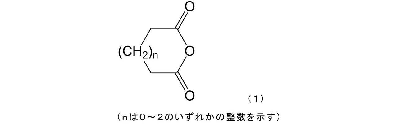


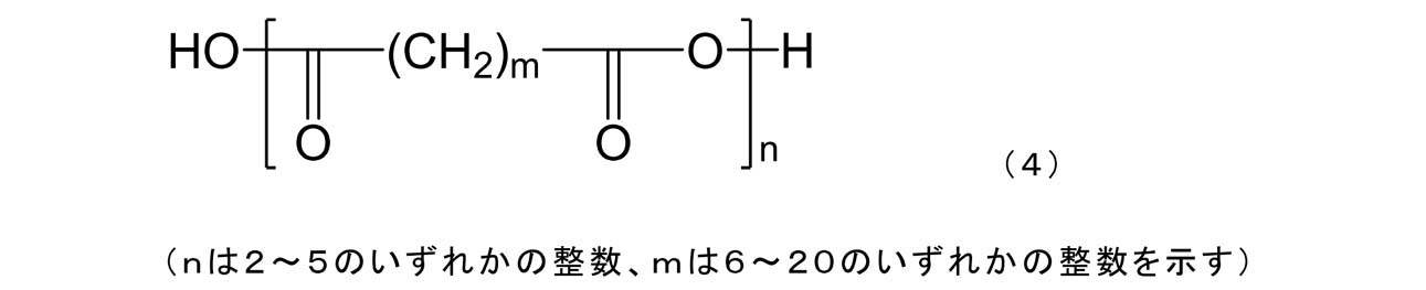
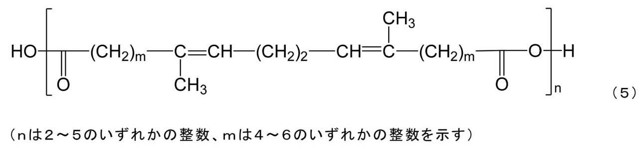
この場合、前記構造式(1)~(3)で表されるカルボン酸無水物は、内部歪のある環状構造を有することから化学的および熱的に開環を生じやすく、また高分子型酸無水物である前記構造式(4)~(5)で表されるカルボン酸無水物は分子内部に加水分解し易い“-(C=O)-O-(C=O)-”というエステル類似構造を有することから化学的および熱的に開環が生じやすい。このため、これらのカルボン酸無水物は加水分解反応の反応性が高く、フラックス成分が低温の加熱温度下で優れたフラックス作用を発揮する。
本発明においては、上記カルボン酸無水物が、コハク酸無水物、グルタル酸無水物、ジグリコール酸無水物、チオジグリコール酸無水物、および下記構造式(6)~(7)で表される高分子型酸無水物からなる群より選択される少なくとも1種の化合物を含むことも好ましい。

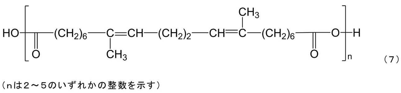
この場合、コハク酸無水物、グルタル酸無水物、ジグリコール酸無水物、チオジグリコール酸無水物は、環状構造の内部歪が特に大きいことから開環が特に生じやすく、また、前記構造式(6)~(7)で示される高分子型酸無水物も分子内部に加水分解し易い“-(C=O)-O-(C=O)-”というエステル類似構造を有することから開環が特に生じやすい。このためこれらのカルボン酸無水物は加水分解反応の反応性が非常に高く、フラックス成分が低温の加熱温度下で特に優れたフラックス作用を発揮する。
また、本発明においては、封止剤組成物が、窒素原子を有する複素環化合物、ポリアミン化合物、およびそのアダクトからなる群より選択される少なくとも1種の化合物を含む反応促進剤を含有することも好ましい。
フラックス成分の添加量は、封止剤組成物全体を100重量部として、0.1~30重量部であることが好ましく、1~10重量部であることがより好ましい。
前記封止剤組成物に含まれる金属粒子の粒径は、特に限定されないが、融解、接合のし易さという観点から、50μm以下であることが好ましく、20μm以下であることが好ましい。また、酸化被膜の影響がでにくい点で、5μm以上であることが好ましく、10μm以上であることがより好ましい。前記封止剤組成物中の金属粒子の充填密度を上げる観点から、異なる粒径の金属粒子を混ぜることも好ましい。なお、粒径は、レーザー回折・散乱法で求めた50%粒径(メディアン粒径)の値を採用する。
また、前記金属粒子は粒径が100nm以下の金属ナノ粒子であってもよい。金属粒子は、粒子サイズを小さくすることで、焼結開始温度(融点)が下がることが知られており、酸化しにくい銀、金などでは、フラックス成分等の添加剤が不要になるという観点から、本発明においては、金属ナノ粒子を好ましく用いることができる。金属ナノ粒子の場合の金属の種類は、特に制限されないが、製造のし易さ、安定性などの観点から、金、銀、銅、白金、銀-銅合金が好ましい。
前記金属ナノ粒子の表面には、アミン化合物が被着していてもよい。金属ナノ粒子に被着したアミン化合物が金属ナノ粒子の表面に保護膜を形成するため、一定数の金属原子が集合して金属ナノ粒子を形成した後は、当該アミンによる保護膜によってそれ以上の金属原子が結合することが困難になると考えられる。このため、粒径の揃った金属ナノ粒子が安定して得られるものと考えられる。
前記アミン化合物としては、例えば、エチレンジアミン、N,N-ジメチルエチレンジアミン、N,N’-ジメチルエチレンジアミン、N,N-ジエチルエチレンジアミン、N,N’-ジエチルエチレンジアミン、1,3-プロパンジアミン、2,2-ジメチル-1,3-プロパンジアミン、N,N-ジメチル-1,3-ジアミノプロパン、N,N’-ジメチル-1,3-ジアミノプロパン、N,N-ジエチル-1,3-ジアミノプロパン、1,4-ジアミノブタン、1,5-ジアミノ-2-メチルペンタン、1,6-ジアミノヘキサン、N,N’-ジメチル-1,6-ジアミノヘキサン、1,7-ジアミノヘプタン、1,8-ジアミノオクタン、2-エトキシエチルアミン、ジプロピルアミン、ジブチルアミン、ヘキシルアミン、シクロヘキシルアミン、ヘプチルアミン、3-ブトキシプロピルアミン、オクチルアミン、ノニルアミン、デシルアミン、3-アミノプロピルトリエトキシシラン、ドデシルアミン、オレイルアミン等が挙げられるが、これらに限定されるものではない。
アミン化合物が被着した金属ナノ粒子の製造方法としては、例えば、金属のシュウ酸塩とアミン化合物とを反応させてその錯化合物を生成させた後、この錯化合物を100~200℃の範囲で低温熱分解させる方法が挙げられる。
前記金属ナノ粒子の粒径は、特に限定されないが、融解、接合のし易さという観点から、50nm以下であることが好ましく、20nm以下であることが好ましい。また、下限値は特に制限されないが、5nm以上であることが好ましく、10nm以上であることがより好ましい。金属粒子の充填密度を上げる観点から、異なる粒径の粒子を混ぜることも好ましい。なお、金属ナノ粒子の粒径は、走査電子顕微鏡で観察した粒径(メディアン粒径)を採用するものとする。
金属粒子の形状は、特に制限されず、例えば、多面体状、正多面体状、球状、回転楕円体状、鱗片状、円盤状、樹枝状、繊維状などが挙げられる。樹脂・金属粒子の混合物の粘度、金属粒子の体積当たりの表面積が小さいといった観点から、球状であることがこのましい。
金属粒子の融点は、特に制限されないが、電子デバイスの製造容易性および熱安定性の観点から、80~200℃であることが好ましく、100~160℃であることがより好ましく、110~140℃であることがさらに好ましい。
封止剤組成物中の前記金属粒子の含有量は、封止剤組成物の全体量を100重量部として、50~90重量部であることが好ましく、60~85重量部であることがより好ましい。
なお、上記金属粒子は、単独でもまたは2種以上組み合わせて用いてもよい。
(封止剤組成物接合体および封止剤組成物に含まれる樹脂)
封止剤組成物接合体および封止剤組成物に含まれる樹脂としては、特に制限されず、熱可塑性樹脂、熱硬化性樹脂、光硬化性樹脂等が挙げられる。硬化性樹脂の場合、封止剤組成物の含まれる樹脂は、未硬化の状態であり、封止剤組成物接合体に含まれる樹脂は、硬化した状態である。
封止剤組成物接合体および封止剤組成物に含まれる樹脂としては、特に制限されず、熱可塑性樹脂、熱硬化性樹脂、光硬化性樹脂等が挙げられる。硬化性樹脂の場合、封止剤組成物の含まれる樹脂は、未硬化の状態であり、封止剤組成物接合体に含まれる樹脂は、硬化した状態である。
より具体的な例としては、例えば、エポキシ樹脂、アクリル樹脂、ポリオレフィン樹脂、フッ素樹脂、ポリ塩化ビニリデン樹脂、アイオノマー樹脂、ウレタン樹脂、エチレン-酢酸ビニル共重合体樹脂、ポリイミド樹脂、シアン酸エステル樹脂、ベンゾオキサジン樹脂等が挙げられる。中でも、エポキシ樹脂およびアクリル樹脂の少なくとも一方を含むことがより好ましい。
(金属粒子を含まない場合の封止剤組成物の粘度)
本発明では、前記封止剤組成物のうち前記金属粒子を除いたときの封止剤組成物(前記樹脂や前記フラックス成分などの金属粒子以外の成分の混合物)において、前記封止剤組成物に内包される前記金属粒子の融点で1分間放置した後の粘度は1Pa・s以下であることが好ましく、100mPa・s以下であることがより好ましい。ここでいう、内包され金属粒子の融点とは、合金の組成から知られている融点を用いる。合金のように、固相からの融点と液相からの融点とが異なる場合は、その平均を融点とする。また、組成の異なる2種以上の金属粒子が混合した場合は、各金属粒子の前記融点の重量平均値を内包する金属の融点とする。なお、前記樹脂の粘度は、E型粘度計により測定した値を採用するものとする。
本発明では、前記封止剤組成物のうち前記金属粒子を除いたときの封止剤組成物(前記樹脂や前記フラックス成分などの金属粒子以外の成分の混合物)において、前記封止剤組成物に内包される前記金属粒子の融点で1分間放置した後の粘度は1Pa・s以下であることが好ましく、100mPa・s以下であることがより好ましい。ここでいう、内包され金属粒子の融点とは、合金の組成から知られている融点を用いる。合金のように、固相からの融点と液相からの融点とが異なる場合は、その平均を融点とする。また、組成の異なる2種以上の金属粒子が混合した場合は、各金属粒子の前記融点の重量平均値を内包する金属の融点とする。なお、前記樹脂の粘度は、E型粘度計により測定した値を採用するものとする。
なお、これらの樹脂は、単独でもまたは2種以上組み合わせて使用してもよく、また、市販品を用いてもよいし合成品を用いてもよい。
前記封止剤組成物接合体ないし封止剤組成物中の前記樹脂の含有量は、封止剤組成物接合体ないし封止剤組成物の全体量を100重量部として、5~50重量部であることが好ましく、10~20重量部であることがより好ましい。
前記封止剤組成物は、前記樹脂の硬化剤を含んでもよい。硬化剤としては、特に制限はなく、上記樹脂に対して反応性を有する官能基を有する化合物であればよい。具体的には、例えば、トリフェニルメタントリイソシアネート、メチレンビス(4-フェニルメタントリイソシアネート)、トリアリルイソシアネート、ダイマー酸ジイソシアネート、2,4-トリレンジイソシアネート(2,4-TDI)、2,6-トリレンジイソシアネート(2,6-TDI)、4,4’-ジフェニルメタンジイソシアネート(4,4’-MDI)、2,4’-ジフェニルメタンジイソシアネート(2,4’-MDI)、1,4-フェニレンジイソシアネート、キシリレンジイソシアネート(XDI)、テトラメチルキシリデンジイソシアネート(TMXDI)、トリジンジイソシアネート(TODI)、1,5-ナフタレンジイソシアネート(NDI)、ヘキサメチレンジイソシアネート(HDI)、トリメチルヘキサメチレンジイソシアネート(TMHDI)、リジンジイソシアネート、ノルボルナンジイソシアナートメチル(NBDI)、トランスシクロヘキサン-1,4-ジイソシアネート、イソホロンジイソシアネート(IPDI)、H6-XDI(水添XDI)、H12-MDI(水添MDI)、上記ジイソシアネートのカルボジイミド変性ジイソシアネート類、またはこれらのイソシアヌレート変性ジイソシアネート類、トリメチロールプロパン/トリレンジイソシアネート3量体付加物などの上記イソシアネート類とトリメチロールプロパン等のポリオール化合物とのアダクト体、これらイソシアネート類のビウレット体やイソシアヌレート体等のイソシアネート系硬化剤;フェノールノボラック樹脂、クレゾールノボラック樹脂、フェノールアラルキル(フェニレン、ビフェニレン骨格を含む)樹脂、ナフトールアラルキル樹脂、トリフェノールメタン樹脂、ジシクロペンタジエン型フェノール樹脂等のフェノール系硬化剤;エチレンジアミン、トリエチレンジアミン、ヘキサメチレンジアミン、2,4-ジアミノ-6-〔2’―メチルイミダゾリル-(1’)〕エチル-s-トリアジン等のトリアジン化合物、1,8-ジアザビシクロ[5,4,0]ウンデセン-7(DBU)、トリエチレンジアミン、ベンジルジメチルアミン、トリエタノールアミン等のアミン系硬化剤;無水フタル酸、無水マレイン酸、ドデセニル無水コハク酸、無水トリメリット酸、ベンゾフェノンテトラカルバン酸二無水物、テトラヒドロ無水フタル酸、ヘキサヒドロ無水フタル酸等の酸無水物系硬化剤;ホルムアルデヒド、アセトアルデヒド、プロピオンアルデヒド、ブチルアルデヒド等のモノアルデヒド類;メチロール尿素、メチロールメラミン、アルキル化メチロール尿素、アルキル化メチロール化メラミン、アセトグアナミン、ベンゾグアナミンとホルムアルデヒドとの縮合物等のアミノ-ホルムアルデヒド樹脂;さらにナトリウム、カリウム、マグネシウム、カルシウム、アルミニウム、鉄、ニッケル、ジルコニウム等の二価金属から四価金属の塩およびその酸化物等が挙げられる。これら硬化剤は、単独でもまたは2種以上組み合わせて用いてもよい。
封止剤組成物中の前記硬化剤の含有量は、封止剤組成物の全体量を100重量部として、1~10重量部であることが好ましい。
前記封止剤組成物は、必要に応じて他の添加剤を含んでもよい。他の添加剤の具体例としては、例えば、トリフェニルスルホニウムヘキサフルオロアンチモネート、トリフェニルスルホニウムホスフェート、p-(フェニルチオ)フェニルジフェニルスルホニウムヘキサフルオロアンチモネート、4-クロルフェニルジフェニルスルホニウムヘキサフルオロホスフェート、ビス[4-(ジフェニルスルフォニオ)フェニル]スルフィドビスヘキサフルオロフォスフェート、ビス[4-(ジフェニルスルフォニオ)フェニル]スルフィドビスヘキサフルオロアンチモネート、ジアリルヨードニウムヘキサフルオロアンチモネート、ジエトキシアセトフェノン、4-(2-ヒドロキシエトキシ)フェニル-(2-ヒドロキシ-2-プロピル)ケトン、2-メチル-2-モルホリノ(4-チオメチルフェニル)プロパン-1-オン、2-ベンジル-2-ジメチルアミノ-1-(4-モルホリノフェニル)-ブタノン、2-ヒドロキシ-2-メチル-1-フェニルプロパン-1-オン、ベンジルジメチルケタール、4-(2-アクリロイル-オキシエトキシ)フェニル-2-ヒドロキシ-2-プロピルケトン、2,4,6-トリメチルベンゾイルジフェニルホスフィンオキサイド等の硬化触媒、レブリン酸等の融剤、シランカップリング剤、硬化促進剤、イオン液体、リチウム塩、無機フィラー、軟化剤、酸化防止剤、老化防止剤、安定剤、粘着付与樹脂、レベリング剤、消泡剤、可塑剤、染料、顔料(着色顔料、体質顔料等)、処理剤、紫外線遮断剤、蛍光増白剤、分散剤、熱安定剤、光安定剤、紫外線吸収剤、帯電防止剤、滑剤等が挙げられる。
前記封止剤組成物接合の原料である前記封止剤組成物は、外部エネルギーにより硬化することにより封止剤組成物接合体を形成するのが好ましい。硬化方法は、特に制限されず、例えば、加熱、紫外線照射、電子線照射、レーザー照射等が挙げられる。
前記封止剤組成物接合体及びその原料である封止剤組成物の配置については、特に制限されないが、図1~4のように、電子素子本体13の外側に配置することが好ましい。このような封止剤組成物接合体及びその原料である封止剤組成物の配置により、本発明の効果をより効率的に得ることができる。
前記封止剤組成物接合体の原料である封止剤組成物は、市販品を用いてもよいし合成品(調製品)を用いてもよい。封止剤組成物を調製する場合は、例えば、上記に示す金属粒子、樹脂、および必要に応じて他の成分を、-20~40℃で、1~24時間の間、攪拌混合する方法が適用される。
本発明に係る封止剤組成物接合体の原料である封止剤組成物の硬化前の25℃における粘度は、100~1000Pa・sであることが好ましい。この範囲であれば、後述する液晶滴下工法(ODF法)におけるダム用封止剤として、塗布することができ、フィル用封止剤を封入することができる。なお、前記封止剤組成物の粘度は、E型粘度計により測定した値を採用するものとする。
[電子素子本体]
電子素子本体は電子デバイスの本体である。図1~図4に示す形態において、電子素子本体は有機EL素子本体である。ただし、本発明の電子素子本体はかような形態に制限されず、ガスバリア性フィルムによる封止が適用されうる公知の電子デバイスの本体が使用できる。例えば、太陽電池(PV)、液晶表示素子(LCD)、電子ペーパー、薄膜トランジスタ、タッチパネル等が挙げられる。これらの電子デバイスの本体の構成についても、特に制限はなく、公知の構成を有しうる。
電子素子本体は電子デバイスの本体である。図1~図4に示す形態において、電子素子本体は有機EL素子本体である。ただし、本発明の電子素子本体はかような形態に制限されず、ガスバリア性フィルムによる封止が適用されうる公知の電子デバイスの本体が使用できる。例えば、太陽電池(PV)、液晶表示素子(LCD)、電子ペーパー、薄膜トランジスタ、タッチパネル等が挙げられる。これらの電子デバイスの本体の構成についても、特に制限はなく、公知の構成を有しうる。
図1~図4に示す形態において、電子素子本体(有機EL素子本体)13は、第1電極(陽極)17、正孔輸送層18、発光層19、電子輸送層20、第2電極(陰極)21等を有する。また、必要に応じて、第1電極17と正孔輸送層18との間に正孔注入層を設けてもよいし、または、電子輸送層20と第2電極21との間に電子注入層を設けてもよい。有機EL素子において、正孔注入層、正孔輸送層18、電子輸送層20、電子注入層は必要に応じて設けられる任意の層である。
以下、具体的な電子デバイスの構成の一例として、有機EL素子を説明する。
(第1電極:陽極)
第1電極(陽極)としては、仕事関数の大きい(4eV以上)金属、合金、電気伝導性化合物およびこれらの混合物を電極物質とするものが好ましく用いられる。
第1電極(陽極)としては、仕事関数の大きい(4eV以上)金属、合金、電気伝導性化合物およびこれらの混合物を電極物質とするものが好ましく用いられる。
(正孔注入層:陽極バッファ層)
第1電極(陽極)と発光層または正孔輸送層の間に、正孔注入層(陽極バッファ層)を存在させてもよい。正孔注入層とは、駆動電圧低下や発光輝度向上のために電極と有機層間に設けられる層である。
第1電極(陽極)と発光層または正孔輸送層の間に、正孔注入層(陽極バッファ層)を存在させてもよい。正孔注入層とは、駆動電圧低下や発光輝度向上のために電極と有機層間に設けられる層である。
(正孔輸送層)
正孔輸送層とは、正孔を輸送する機能を有する正孔輸送材料からなり、広い意味で正孔注入層、電子阻止層も正孔輸送層に含まれる。正孔輸送層は単層または複数層設けることが出来る。
正孔輸送層とは、正孔を輸送する機能を有する正孔輸送材料からなり、広い意味で正孔注入層、電子阻止層も正孔輸送層に含まれる。正孔輸送層は単層または複数層設けることが出来る。
(発光層)
発光層とは、青色発光層、緑色発光層、赤色発光層を指す。発光層を積層する場合の積層順としては、特に制限はなく、また各発光層間に非発光性の中間層を有していてもよい。
発光層とは、青色発光層、緑色発光層、赤色発光層を指す。発光層を積層する場合の積層順としては、特に制限はなく、また各発光層間に非発光性の中間層を有していてもよい。
(電子輸送層)
電子輸送層とは、電子を輸送する機能を有する材料からなり広い意味で電子輸送層に含まれる。電子注入層とは、駆動電圧低下や発光輝度向上のために電極と有機層間に設けられる層である。
電子輸送層とは、電子を輸送する機能を有する材料からなり広い意味で電子輸送層に含まれる。電子注入層とは、駆動電圧低下や発光輝度向上のために電極と有機層間に設けられる層である。
(電子注入層:陰極バッファ層)
電子注入層形成工程で形成される電子注入層(陰極バッファ層)とは、電子を輸送する機能を有する材料からなり広い意味で電子輸送層に含まれる。電子注入層とは、駆動電圧低下や発光輝度向上のために電極と有機層間に設けられる層である。
電子注入層形成工程で形成される電子注入層(陰極バッファ層)とは、電子を輸送する機能を有する材料からなり広い意味で電子輸送層に含まれる。電子注入層とは、駆動電圧低下や発光輝度向上のために電極と有機層間に設けられる層である。
(第2電極:陰極)
第2電極(陰極)としては、仕事関数の小さい(4eV以下)金属(電子注入性金属と称する)、合金、電気伝導性化合物およびこれらの混合物を電極物質とするものが用いられる。
第2電極(陰極)としては、仕事関数の小さい(4eV以下)金属(電子注入性金属と称する)、合金、電気伝導性化合物およびこれらの混合物を電極物質とするものが用いられる。
(保護層)
図2に示すように、本発明の電子デバイスは、必要に応じて、電子素子本体上に保護層を有してもよい。保護層は、水分や酸素等の電子素子本体の劣化を促進するものが素子内に侵入することを防止する機能、基材11上に配置された電子素子本体等を絶縁性とする機能、または電子素子本体による段差を解消する機能を有する。保護層は、1層でもよいし、複数の層を積層してもよい。本発明では、保護層によって、封止剤組成物と電子デバイスとが絶縁されていることが好ましい。
図2に示すように、本発明の電子デバイスは、必要に応じて、電子素子本体上に保護層を有してもよい。保護層は、水分や酸素等の電子素子本体の劣化を促進するものが素子内に侵入することを防止する機能、基材11上に配置された電子素子本体等を絶縁性とする機能、または電子素子本体による段差を解消する機能を有する。保護層は、1層でもよいし、複数の層を積層してもよい。本発明では、保護層によって、封止剤組成物と電子デバイスとが絶縁されていることが好ましい。
(電子デバイスの製造方法)
本発明の電子デバイス10の製造方法は特に制限されず、従来公知の知見が適宜参照されうる。
本発明の電子デバイス10の製造方法は特に制限されず、従来公知の知見が適宜参照されうる。
本発明の一実施形態によれば、(1)基材上に電子素子本体を配置する工程と、(2)封止部材上に前記封止剤組成物接合体形成用原料の前記封止剤組成物を塗布する工程と、(3)基材および電子素子本体上に封止部材を配置する工程と、(4)前記封止剤組成物中の金属粒子を溶融し金属相を形成する工程と、(5)前記封止剤組成物中の樹脂を硬化させる工程と、を含む電子デバイスの製造方法が提供される。
以下、上記本発明の一実施形態による電子デバイスの製造方法を説明するが、本発明はこれに何ら限定されるものではない。
(1)基材上に電子素子本体を配置する工程
まず、基材上に電子素子本体を配置する。通常、基材上に、電子素子本体を構成する層、例えば、第1電極層、正孔注入層、正孔輸送層、発光層、電子輸送層、電子注入層、第2電極層等を順に積層させることにより形成される。これらの形成方法は特に制限されず、公知の手法を適宜参照して製造されうる。
まず、基材上に電子素子本体を配置する。通常、基材上に、電子素子本体を構成する層、例えば、第1電極層、正孔注入層、正孔輸送層、発光層、電子輸送層、電子注入層、第2電極層等を順に積層させることにより形成される。これらの形成方法は特に制限されず、公知の手法を適宜参照して製造されうる。
次いで、必要に応じて、保護層を形成させる。保護層の形成方法も特に制限されず、公知の手法を適宜参照して製造されうる。
(2)封止部材上に前記封止剤組成物接合体の形成用原料である前記封止剤組成物を塗布する工程
次いで、前記封止部材上に前記封止剤組成物を塗布し、塗膜を形成する。例えば、図1~図4に示す形態の電子デバイス10を製造する場合には、基材11の中心部上に配置した電子素子本体13の周囲を取り囲むように封止部材12の周囲部(外周部)上に帯状に封止剤組成物14’を塗布すればよい。
次いで、前記封止部材上に前記封止剤組成物を塗布し、塗膜を形成する。例えば、図1~図4に示す形態の電子デバイス10を製造する場合には、基材11の中心部上に配置した電子素子本体13の周囲を取り囲むように封止部材12の周囲部(外周部)上に帯状に封止剤組成物14’を塗布すればよい。
封止剤組成物の塗布方法としては、例えば、マイクログラビアコート法、グラビアコート法、バーコート法、ワイヤーバーコート法、ロールコート法、ディップコート法、フレキソ印刷法、オフセット印刷法、スクリーン印刷法等が挙げられる。封止剤量のコントロールのしやすさから、好ましくは、ディスペンサーにより液状の封止剤組成物を塗布する液晶滴下工法(ODF、One Drop Filling)が用いられる。
必要に応じて、図2に示すように、封止剤組成物接続体14の形成用原料である前記封止剤組成物(図3、4の符号14’参照)よりも内側にフィル用封止剤16を塗布する。図2に示す形態のように電子素子本体13の上面に塗布されてもよいし、保護層15を有する場合は保護層15の上面に塗布されてもよいし、電子素子本体13の一部または全部の構成層の上面に形成してもよい。
フィル用封止剤の例としては、例えば、エポキシ樹脂、アクリル樹脂、ポリオレフィン樹脂、フッ素樹脂、ポリ塩化ビニリデン樹脂等を含む封止剤が挙げられる。該フィル用封止剤は、硬化剤を含んでもよい。また、これらの樹脂は、単独でもまたは2種以上組み合わせて使用してもよい。
(3)基材および電子素子本体上に封止部材を配置する工程
続いて、図1~4に示すように、前記基材11および前記電子素子本体13の上部を覆うように、封止部材12を配置する。
続いて、図1~4に示すように、前記基材11および前記電子素子本体13の上部を覆うように、封止部材12を配置する。
(4)封止剤組成物接続体の形成用原料である封止剤組成物中の金属粒子を溶融し、基材および封止部材と結着する金属相を形成する工程
次に、図3~4に示すように、封止剤組成物14’中の少なくとも一部の金属粒子14aを溶融し凝集させ、前記基材11および前記封止部材12と結着する金属相14cを形成する。
次に、図3~4に示すように、封止剤組成物14’中の少なくとも一部の金属粒子14aを溶融し凝集させ、前記基材11および前記封止部材12と結着する金属相14cを形成する。
金属粒子の溶融方法は、特に制限されず、例えば、加熱等が挙げられる。
加熱により金属粒子を溶融する際の加熱温度は、特に制限されないが、100~200℃であることが好ましい。また、加熱時間は、1分~30分であることが好ましい。
(5)封止剤組成物中の樹脂を硬化する工程(封止剤組成物接合体形成工程)
最後に、図3~4に示すように、封止剤組成物14’中の樹脂14bを硬化する。これにより、封止剤組成物接合体14が形成され、前記基材11と前記封止部材12とが、前記封止剤組成物接合体14を介して接合され前記電子素子本体13が封止され、電子デバイス10が形成される。
最後に、図3~4に示すように、封止剤組成物14’中の樹脂14bを硬化する。これにより、封止剤組成物接合体14が形成され、前記基材11と前記封止部材12とが、前記封止剤組成物接合体14を介して接合され前記電子素子本体13が封止され、電子デバイス10が形成される。
前記封止剤組成物14’中の樹脂14bの硬化方法は、特に制限されず、例えば、加熱、紫外線照射、電子線照射、レーザー照射等が挙げられる。なお、加熱やレーザー照射により硬化を行う場合、本工程は上記(4)の工程を兼ねるものであってもよい。すなわち、一度の加熱またはレーザー照射により上記(4)の工程と、本工程とが行われてもよい。
上記の製造方法の他、図1~4に示すように、(1)封止部材12上に電子素子本体13を配置する工程と、(2)基材11上に封止剤組成物14’を塗布する工程と、(3)封止部材12および電子素子本体13上に基材11を配置する工程と、(4)封止剤組成物14’中の金属粒子14aを溶融し金属相14cを形成する工程と、(5)封止剤組成物14’中の樹脂14bを硬化させる(封止剤組成物接合体14を形成する)工程と、を含む電子デバイス10の製造方法が挙げられる。
本発明の効果を、以下の実施例および比較例を用いて説明する。ただし、本発明の技術的範囲が以下の実施例のみに制限されるわけではない。また、実施例において「部」あるいは「%」の表示を用いるが、特に断りがない限り「質量部」あるいは「質量%」を表す。
〔ガスバリア性フィルム1の作製〕
《支持体の作製》
〈支持体(ア)の作製〉
熱可塑性樹脂支持体として、両面に易接着加工された厚さ125μmのポリエチレンナフタレートフィルム(帝人デュポンフィルム株式会社製、Q65FWA)を用い、下記に示すように、片面にブリードアウト防止層を、反対面に平滑層を形成したものを支持体(ア)とした。
《支持体の作製》
〈支持体(ア)の作製〉
熱可塑性樹脂支持体として、両面に易接着加工された厚さ125μmのポリエチレンナフタレートフィルム(帝人デュポンフィルム株式会社製、Q65FWA)を用い、下記に示すように、片面にブリードアウト防止層を、反対面に平滑層を形成したものを支持体(ア)とした。
〈ブリードアウト防止層の形成〉
上記熱可塑性樹脂支持体の一方の面側に、JSR株式会社製のUV硬化型有機/無機ハイブリッドハードコート材 OPSTAR(登録商標)Z7535を、乾燥後の膜厚が4.0μmになる条件で塗布した後、硬化条件として、照射エネルギー量1J/cm2で、空気雰囲気下、高圧水銀ランプを使用し、乾燥条件80℃で、3分間の硬化処理を行い、ブリードアウト防止層を形成した。
上記熱可塑性樹脂支持体の一方の面側に、JSR株式会社製のUV硬化型有機/無機ハイブリッドハードコート材 OPSTAR(登録商標)Z7535を、乾燥後の膜厚が4.0μmになる条件で塗布した後、硬化条件として、照射エネルギー量1J/cm2で、空気雰囲気下、高圧水銀ランプを使用し、乾燥条件80℃で、3分間の硬化処理を行い、ブリードアウト防止層を形成した。
〈平滑層の形成〉
次いで、上記熱可塑性樹脂支持体のブリードアウト防止層を形成した面とは反対側の面側に、JSR株式会社製のUV硬化型有機/無機ハイブリッドハードコート材 OPSTAR(登録商標)Z7501を、乾燥後の膜厚が4.0μmになる条件で塗布した後、80℃で、3分間乾燥した後、空気雰囲気下、高圧水銀ランプを使用し、硬化条件として、照射エネルギー量1J/cm2で照射、硬化して、平滑層を形成した。
次いで、上記熱可塑性樹脂支持体のブリードアウト防止層を形成した面とは反対側の面側に、JSR株式会社製のUV硬化型有機/無機ハイブリッドハードコート材 OPSTAR(登録商標)Z7501を、乾燥後の膜厚が4.0μmになる条件で塗布した後、80℃で、3分間乾燥した後、空気雰囲気下、高圧水銀ランプを使用し、硬化条件として、照射エネルギー量1J/cm2で照射、硬化して、平滑層を形成した。
得られた平滑層のJIS B 0601:2001で規定される方法に準拠して測定した表面粗さRaは1nmであった。また、Rzは20nmであった。平滑層の塗布面はアンカーコート層の面とした。
表面粗さは、SII社製のAFM(原子間力顕微鏡)SPI3800N DFMを用いて測定した。一回の測定範囲は80μm×80μmとし、測定箇所を変えて三回の測定を行って、それぞれの測定で得られたRaの値、および、10点平均粗さRzをそれぞれ平均したものを測定値とした。
《ガスバリア層の形成》
〈ポリシラザン層1の形成〉
支持体(ア)の平滑層の上に、下記ポリシラザンを含有する塗布液(ポリシラザン含有塗布液1)を、スピンコーターを用いて、塗布スピード30m/minで乾燥後の膜厚が150nmとなる条件で塗布した。乾燥条件は、100℃で2分とした。
〈ポリシラザン層1の形成〉
支持体(ア)の平滑層の上に、下記ポリシラザンを含有する塗布液(ポリシラザン含有塗布液1)を、スピンコーターを用いて、塗布スピード30m/minで乾燥後の膜厚が150nmとなる条件で塗布した。乾燥条件は、100℃で2分とした。
〈ポリシラザン含有塗布液1の調製〉
無触媒のパーヒドロポリシラザンを20質量%含むジブチルエーテル溶液(AZエレクトロニックマテリアルズ株式会社製、NN120-20)と、アミン触媒として1質量%のN,N,N’,N’-テトラメチル-1,6-ジアミノヘキサンおよび19質量%のパーヒドロポリシラザンを含むジブチルエーテル溶液(AZエレクトロニックマテリアルズ株式会社製、NAX120-20)とを、4:1の比率で混合し、アミン触媒の含有量を塗布液の固形分に対して1質量%に調整した。
無触媒のパーヒドロポリシラザンを20質量%含むジブチルエーテル溶液(AZエレクトロニックマテリアルズ株式会社製、NN120-20)と、アミン触媒として1質量%のN,N,N’,N’-テトラメチル-1,6-ジアミノヘキサンおよび19質量%のパーヒドロポリシラザンを含むジブチルエーテル溶液(AZエレクトロニックマテリアルズ株式会社製、NAX120-20)とを、4:1の比率で混合し、アミン触媒の含有量を塗布液の固形分に対して1質量%に調整した。
〈真空紫外線照射処理〉
上記の様にしてポリシラザン層1を形成した後、窒素雰囲気下(酸素濃度:1000ppm)で172nmの真空紫外線を、照射エネルギー量が3000mJ/cm2になるように照射処理を行い、改質を行った。
上記の様にしてポリシラザン層1を形成した後、窒素雰囲気下(酸素濃度:1000ppm)で172nmの真空紫外線を、照射エネルギー量が3000mJ/cm2になるように照射処理を行い、改質を行った。
〈ポリシラザン層2の形成〉
さらに前記ポリシラザン含有塗布液1を、上記で得られたポリシラザン層1上に同様に塗布し、真空紫外線照射(照射量:1700mJ/cm2)を行い、ポリシラザン層1上に乾燥膜厚が50nmであるポリシラザン層2が積層されたガスバリア層1を平滑層上に形成した。
さらに前記ポリシラザン含有塗布液1を、上記で得られたポリシラザン層1上に同様に塗布し、真空紫外線照射(照射量:1700mJ/cm2)を行い、ポリシラザン層1上に乾燥膜厚が50nmであるポリシラザン層2が積層されたガスバリア層1を平滑層上に形成した。
X線光電子分光(XPS)装置(アルバック・ファイ社製、QuanteraSXM)による分析の結果、ガスバリア層1の組成は、SiONであり、ガスバリア層1の厚さ(ポリシラザン層1およびポリシラザン層2の合計厚さ)は200nmであった。
得られたガスバリア性フィルム1について、特開2012-000546号公報に記載のCa法により、水蒸気透過度(WVTR)(60℃、相対湿度90%RH)を測定したところ、WVTR(60℃、90%RH)は、4×10⁻⁵g/m2・24hであった。
〔ガスバリア性フィルム2の作製〕
〈酸素含有炭化ケイ素層の形成〉
支持体(ア)の平滑層の上に、図5に示す製造装置を用いて、プラズマCVD法を用いて、酸素含有炭化ケイ素からなる無機層を形成した。積層フィルムの成膜条件は、ヘキサメチルジシロキサンの供給量が、支持体(ア)の面積速度1m2あたり、0℃、1気圧換算で285sccm、酸素ガスの供給量が、支持体(ア)の面積速度1m2あたり、0℃、1気圧換算で2860sccm、真空チャンバ内の真空度が3Pa、プラズマ発生用電源からの印加電力が0.8kW、プラズマ発生用電源の周波数が70kHz、支持体(ア)の搬送速度が0.5m/minで実施した。得られた積層フィルムにおける薄膜層の厚みは0.3μmであった。
〈酸素含有炭化ケイ素層の形成〉
支持体(ア)の平滑層の上に、図5に示す製造装置を用いて、プラズマCVD法を用いて、酸素含有炭化ケイ素からなる無機層を形成した。積層フィルムの成膜条件は、ヘキサメチルジシロキサンの供給量が、支持体(ア)の面積速度1m2あたり、0℃、1気圧換算で285sccm、酸素ガスの供給量が、支持体(ア)の面積速度1m2あたり、0℃、1気圧換算で2860sccm、真空チャンバ内の真空度が3Pa、プラズマ発生用電源からの印加電力が0.8kW、プラズマ発生用電源の周波数が70kHz、支持体(ア)の搬送速度が0.5m/minで実施した。得られた積層フィルムにおける薄膜層の厚みは0.3μmであった。
ここで、図5に示す製造装置31は、送り出しローラー32と、搬送ローラー33、34、35、36と、成膜ローラー39、40と、ガス供給管41と、プラズマ発生用電源42と、成膜ローラー39および40の内部に設置された磁場発生装置43、44と、巻取りローラー45とを備えている。また、製造装置31においては、成膜ローラー39、40と、ガス供給管41と、プラズマ発生用電源42と、磁場発生装置43、44とが図示を省略した真空チャンバ内に配置されている。さらに製造装置31において前記真空チャンバは図示を省略した真空ポンプに接続されており、かかる真空ポンプにより真空チャンバ内の圧力を調整できるものを使用した。かかる図5に示す製造装置31を用いて、上記した積層フィルム1の成膜条件下で、成膜ガス(原料ガス等)を真空チャンバ内に供給しつつ、一対の成膜ローラー(成膜ローラー39および40)間に放電を発生させることにより、前記成膜ガス(原料ガス等)がプラズマによって分解され、成膜ローラー39上の基材2の表面上および成膜ローラー40上の支持体(ア)2の表面上に、酸素含有炭化ケイ素からなる無機層3がプラズマCVD法により形成されてなる積層フィルム1を作製した。
積層フィルムの膜表面からの各距離における原子比を、X線光電子分光(XPS)装置(アルバック・ファイ社製、QuanteraSXM)を用いた深さ方向の元素組成分析によって確認したところ、炭素分布曲線に極値を有し、炭素濃度の極大と極小との差が7at%であることを確認した。
〈ポリシラザン層の形成〉
さらに前記ポリシラザン含有塗布液1を、上記で得られた無機層上にガスバリアフィルム1と同様に塗布し、真空紫外線照射(照射量:2000mJ/cm2)を行い、酸素含有炭化ケイ素からなる層上に乾燥膜厚が50nmであるポリシラザン層が積層されたガスバリア層2を、支持体(ア)の平滑層上に形成し、ガスバリア性フィルム2を得た。
さらに前記ポリシラザン含有塗布液1を、上記で得られた無機層上にガスバリアフィルム1と同様に塗布し、真空紫外線照射(照射量:2000mJ/cm2)を行い、酸素含有炭化ケイ素からなる層上に乾燥膜厚が50nmであるポリシラザン層が積層されたガスバリア層2を、支持体(ア)の平滑層上に形成し、ガスバリア性フィルム2を得た。
得られたガスバリア性フィルム2について、特開2012-000546号公報に記載のCa法により、水蒸気透過度(WVTR)(60℃、90%RH)を測定したところ、7×10⁻⁶g/m2・24hであった。
〔ガスバリア性フィルム3の作製〕
《支持体の作製》
〈支持体(イ)の作製〉
熱可塑性樹脂支持体として、両面に易接着加工された厚さ125μmのポリエチレンナフタレートフィルム(帝人デュポンフィルム株式会社製、Q65FWA)を用い、支持体(イ)とした。
《支持体の作製》
〈支持体(イ)の作製〉
熱可塑性樹脂支持体として、両面に易接着加工された厚さ125μmのポリエチレンナフタレートフィルム(帝人デュポンフィルム株式会社製、Q65FWA)を用い、支持体(イ)とした。
《ガスバリア層の形成》
上記支持体(イ)上に、国際公開第2012/003198号の実施例1に記載の方法と同様の方法で無機層(厚さ30nmのSiAlOx膜)と有機層とを、それぞれ3層ずつ積層したガスバリア層3を設け、ガスバリア性フィルム3を作製した。
上記支持体(イ)上に、国際公開第2012/003198号の実施例1に記載の方法と同様の方法で無機層(厚さ30nmのSiAlOx膜)と有機層とを、それぞれ3層ずつ積層したガスバリア層3を設け、ガスバリア性フィルム3を作製した。
得られたガスバリア性フィルム3について、特開2012-000546号公報に記載のCa法により、水蒸気透過度(WVTR)(60℃、90%RH)を測定したところ、4×10⁻⁵g/m2・24hであった。
〔ガスバリア性フィルム4の作製〕
ガスバリア層3の代わりに、国際公開第2011/013341号の実施例E2に記載の方法と同様の方法で作製したバリア膜(厚さ30nmのSiO2膜)を3枚貼りあわせて、有機層および無機層が積層されたガスバリア層4を作製したこと以外は、ガスバリア性フィルム3と同様にして、ガスバリア性フィルム4を作製した。
ガスバリア層3の代わりに、国際公開第2011/013341号の実施例E2に記載の方法と同様の方法で作製したバリア膜(厚さ30nmのSiO2膜)を3枚貼りあわせて、有機層および無機層が積層されたガスバリア層4を作製したこと以外は、ガスバリア性フィルム3と同様にして、ガスバリア性フィルム4を作製した。
得られたガスバリア性フィルム4について、特開2012-000546号公報に記載のCa法により、水蒸気透過度(WVTR)(60℃、90%RH)を測定したところ、5×10⁻⁵g/m2・24hであった。
〔封止剤組成物の作製〕
〈比較封止剤組成物 DT-1〉
無機フィラーとして平均粒径6μmのシリカ粒子 30重量部、液状エポキシ樹脂(新日鐵化学株式会社製、YD128)11重量部、および硬化剤(味の素ファインテクノ株式会社製、アミキュア(登録商標)PN-23)2重量部を、ディスパーを用いて均一に混合し(混合温度25℃、混合時間1時間)、封止剤組成物DT-1を得た。E型粘度計で測定したDT-1の粘度は、150Pa(25℃)であった。
〈比較封止剤組成物 DT-1〉
無機フィラーとして平均粒径6μmのシリカ粒子 30重量部、液状エポキシ樹脂(新日鐵化学株式会社製、YD128)11重量部、および硬化剤(味の素ファインテクノ株式会社製、アミキュア(登録商標)PN-23)2重量部を、ディスパーを用いて均一に混合し(混合温度25℃、混合時間1時間)、封止剤組成物DT-1を得た。E型粘度計で測定したDT-1の粘度は、150Pa(25℃)であった。
〈封止剤組成物 DT-2〉
はんだ粒子として、Sn42Bi58を用い、常法に従い、はんだ粒子を作製した。作製したはんだ粒子の平均粒径は15μm、融点は138℃であった。このはんだ粒子 85重量部、液状エポキシ樹脂(新日鐵化学株式会社製、YD128、)11重量部、硬化剤(味の素ファインテクノ株式会社製、アミキュア(登録商標)PN-23)2重量部、および融剤としてレブリン酸2重量部を、ディスパーを用いて均一に混合し(混合温度25℃、混合時間1時間)、封止剤組成物DT-2を得た。E型粘度計で測定したDT-2の粘度は、200Pa(25℃)であった。金属粒子以外の混合物の138℃で1分間放置した後の粘度は30mPa・sであった。
はんだ粒子として、Sn42Bi58を用い、常法に従い、はんだ粒子を作製した。作製したはんだ粒子の平均粒径は15μm、融点は138℃であった。このはんだ粒子 85重量部、液状エポキシ樹脂(新日鐵化学株式会社製、YD128、)11重量部、硬化剤(味の素ファインテクノ株式会社製、アミキュア(登録商標)PN-23)2重量部、および融剤としてレブリン酸2重量部を、ディスパーを用いて均一に混合し(混合温度25℃、混合時間1時間)、封止剤組成物DT-2を得た。E型粘度計で測定したDT-2の粘度は、200Pa(25℃)であった。金属粒子以外の混合物の138℃で1分間放置した後の粘度は30mPa・sであった。
〈封止剤組成物 DT-3〉
はんだ粒子として、In58Sn42を用い、常法に従い、はんだ粒子を作製した。作製したはんだ粒子の平均粒径は15μm、融点は118℃であった。このはんだ粒子 85重量部、液状エポキシ樹脂(新日鐵化学株式会社製、YD128)11重量部、硬化剤(味の素ファインテクノ株式会社製、アミキュア(登録商標)PN-23)2重量部、および融剤としてレブリン酸2重量部を、ディスパーを用いて均一に混合し(混合温度25℃、混合時間1時間)、封止剤組成物DT-3を得た。E型粘度計で測定したDT-3の粘度は、250Pa(25℃)であった。金属粒子以外の混合物の118℃で1分間放置した後の粘度は80mPa・sであった。
はんだ粒子として、In58Sn42を用い、常法に従い、はんだ粒子を作製した。作製したはんだ粒子の平均粒径は15μm、融点は118℃であった。このはんだ粒子 85重量部、液状エポキシ樹脂(新日鐵化学株式会社製、YD128)11重量部、硬化剤(味の素ファインテクノ株式会社製、アミキュア(登録商標)PN-23)2重量部、および融剤としてレブリン酸2重量部を、ディスパーを用いて均一に混合し(混合温度25℃、混合時間1時間)、封止剤組成物DT-3を得た。E型粘度計で測定したDT-3の粘度は、250Pa(25℃)であった。金属粒子以外の混合物の118℃で1分間放置した後の粘度は80mPa・sであった。
〈封止剤組成物 DT-4〉
オレイルアミン 5.35g(20mmol)、ヘキシルアミン 2.02g(20mmol)およびメタノール5mlを混合し、この混合溶液にシュウ酸銀 1.519g(5mmol)を添加し、さらに水1mlを添加して、室温で2時間攪拌してシュウ酸銀を溶解させた。このとき得られた生成物は、FT-IRを用いた解析により、銀、シュウ酸イオン、オレイルアミンおよびヘキシルアミンを含む錯化合物であることを確認した。
オレイルアミン 5.35g(20mmol)、ヘキシルアミン 2.02g(20mmol)およびメタノール5mlを混合し、この混合溶液にシュウ酸銀 1.519g(5mmol)を添加し、さらに水1mlを添加して、室温で2時間攪拌してシュウ酸銀を溶解させた。このとき得られた生成物は、FT-IRを用いた解析により、銀、シュウ酸イオン、オレイルアミンおよびヘキシルアミンを含む錯化合物であることを確認した。
その後、エバポレータを使用して40℃でメタノールを除去し、次いで、150℃に加熱して1時間攪拌させることにより、褐色の液体を得た。これにヘキサン30mlを加えて約30分間攪拌し、遠心分離機で分離させ上澄みを濾過した。この操作を3回繰り返した。さらに、エバポレータを使用して45℃でヘキサンを除去した後、メタノール20mlを加えて遠心分離機で分離させ上澄みを除去した。この操作も3回繰り返し、その後、減圧乾燥により生成物として金属銀および金属銀に吸着した有機物からなる、粉末の金属ナノ粒子NP-Aを得た(融点(焼結開始温度):115℃)。得られた粉末について以下のような解析および評価を行った。
得られた粉末について、X線回折装置(株式会社リガク製、ミニフレックス)により解析を行ったところ、X線回折パターンから金属銀が生成されていることを確認した。
また、走査透過電子顕微鏡による観察を行い、NP-Aが、粒径12.5nmの粒度の揃った球状の単分散超微粒子からなるものであったことを確認した。銀としての収率は87.8%であった。また、IR分析によりオレイルアミンとヘキシルアミンとが被着していることを確認した。Agの重量比は90%であった。
上記で得られたNP-A 85重量部、液状エポキシ樹脂(新日鐵化学株式会社製、YD128)11重量部、および硬化剤(味の素ファインテクノ株式会社製、アミキュア(登録商標)PN-23)2重量部を、ディスパーを用いて均一に混合し(混合温度25℃、混合時間1時間)、封止剤組成物DT-4を得た。E型粘度計で測定したDT-4の粘度は、300Pa(25℃)であった。金属粒子以外の混合物の115℃で1分間放置した後の粘度:100mPa・sであった。
〈フィル用封止剤 FT-1〉
液状エポキシ樹脂(新日鐵化学株式会社製、YD128)11重量部、および硬化剤(味の素ファインテクノ株式会社製、アミキュア(登録商標)PN-23)2重量部を、ディスパーを用いて均一に混合し(混合温度25℃、混合時間1時間)、封止剤組成物FT-1を得た。E型粘度計で測定したFT-1の粘度は、750mPa(25℃)であった。
液状エポキシ樹脂(新日鐵化学株式会社製、YD128)11重量部、および硬化剤(味の素ファインテクノ株式会社製、アミキュア(登録商標)PN-23)2重量部を、ディスパーを用いて均一に混合し(混合温度25℃、混合時間1時間)、封止剤組成物FT-1を得た。E型粘度計で測定したFT-1の粘度は、750mPa(25℃)であった。
(実施例1)
《電子デバイスの作製》
0.7mm厚の無アルカリガラスを基材として用いて、以下の手順で、有機薄膜電子デバイスである有機EL素子を作製した。
《電子デバイスの作製》
0.7mm厚の無アルカリガラスを基材として用いて、以下の手順で、有機薄膜電子デバイスである有機EL素子を作製した。
〔有機EL素子の作製〕
(第1電極層の形成)
ガスバリア性フィルム1のガスバリア層上に、厚さ150nmのITO(酸化インジウムスズ)をスパッタ法により成膜し、フォトリソグラフィー法によりパターニングを行い、第1電極層を形成した。
(第1電極層の形成)
ガスバリア性フィルム1のガスバリア層上に、厚さ150nmのITO(酸化インジウムスズ)をスパッタ法により成膜し、フォトリソグラフィー法によりパターニングを行い、第1電極層を形成した。
(正孔輸送層の形成)
上記で形成した第1電極層の上に、以下に示す正孔輸送層形成用塗布液を、乾燥後の厚みが50nmとなるように押出し塗布機で塗布した後乾燥し、正孔輸送層を形成した。
上記で形成した第1電極層の上に、以下に示す正孔輸送層形成用塗布液を、乾燥後の厚みが50nmとなるように押出し塗布機で塗布した後乾燥し、正孔輸送層を形成した。
正孔輸送層形成用塗布液を塗布する前に、ガスバリア性フィルムの洗浄表面改質処理を、波長184.9nmの低圧水銀ランプを使用し、照射強度15mW/cm2、距離10mmで実施した。帯電除去処理は、微弱X線による除電器を使用し行った。
〈塗布条件〉
塗布工程は大気中、25℃、相対湿度50%RHの環境で行った。
塗布工程は大気中、25℃、相対湿度50%RHの環境で行った。
〈正孔輸送層形成用塗布液の準備〉
ポリエチレンジオキシチオフェン・ポリスチレンスルホネート(PEDOT/PSS、Bayer社製 Baytron(登録商標)P AI 4083)を純水で65%、およびメタノール5%で希釈した溶液を正孔輸送層形成用塗布液として準備した。
ポリエチレンジオキシチオフェン・ポリスチレンスルホネート(PEDOT/PSS、Bayer社製 Baytron(登録商標)P AI 4083)を純水で65%、およびメタノール5%で希釈した溶液を正孔輸送層形成用塗布液として準備した。
〈乾燥および加熱処理条件〉
正孔輸送層形成用塗布液を塗布した後、成膜面に向け高さ100mm、吐出風速1m/s、幅手の風速分布5%、温度100℃で温風を当て溶媒を除去した後、引き続き、加熱処理装置を用い、温度150℃で裏面伝熱方式の熱処理を行い、正孔輸送層を形成した。
正孔輸送層形成用塗布液を塗布した後、成膜面に向け高さ100mm、吐出風速1m/s、幅手の風速分布5%、温度100℃で温風を当て溶媒を除去した後、引き続き、加熱処理装置を用い、温度150℃で裏面伝熱方式の熱処理を行い、正孔輸送層を形成した。
(発光層の形成)
引き続き、上記で形成した正孔輸送層の上に、以下に示す白色発光層形成用塗布液を乾燥後の厚みが40nmになるように押出し塗布機で塗布した後乾燥し、発光層を形成した。
引き続き、上記で形成した正孔輸送層の上に、以下に示す白色発光層形成用塗布液を乾燥後の厚みが40nmになるように押出し塗布機で塗布した後乾燥し、発光層を形成した。
〈白色発光層形成用塗布液〉
ホスト材H-A 1.0g、ドーパント材D-A 100mg、ドーパント材D-B 0.2mg、およびドーパント材D-C 0.2mgを、100gのトルエンに溶解し白色発光層形成用塗布液として準備した。ホスト材H-A、ドーパント材D-A、ドーパント材D-B、およびドーパント材D-Cの化学構造は、下記化学式に示す通りである。
ホスト材H-A 1.0g、ドーパント材D-A 100mg、ドーパント材D-B 0.2mg、およびドーパント材D-C 0.2mgを、100gのトルエンに溶解し白色発光層形成用塗布液として準備した。ホスト材H-A、ドーパント材D-A、ドーパント材D-B、およびドーパント材D-Cの化学構造は、下記化学式に示す通りである。

〈塗布条件〉
塗布工程を、窒素ガス濃度99%以上の雰囲気で、塗布温度を25℃とし、塗布速度1m/minで行った。
塗布工程を、窒素ガス濃度99%以上の雰囲気で、塗布温度を25℃とし、塗布速度1m/minで行った。
〈乾燥および加熱処理条件〉
白色発光層形成用塗布液を塗布した後、成膜面に向け高さ100mm、吐出風速1m/s、幅手の風速分布5%、温度60℃で温風を当て溶媒を除去した後、引き続き、温度130℃で加熱処理を行い、発光層を形成した。
白色発光層形成用塗布液を塗布した後、成膜面に向け高さ100mm、吐出風速1m/s、幅手の風速分布5%、温度60℃で温風を当て溶媒を除去した後、引き続き、温度130℃で加熱処理を行い、発光層を形成した。
(電子輸送層の形成)
引き続き、上記で形成した発光層の上に、以下に示す電子輸送層形成用塗布液を、乾燥後の厚みが30nmになるように押出し塗布機で塗布した後、乾燥し電子輸送層を形成した。
引き続き、上記で形成した発光層の上に、以下に示す電子輸送層形成用塗布液を、乾燥後の厚みが30nmになるように押出し塗布機で塗布した後、乾燥し電子輸送層を形成した。
〈塗布条件〉
塗布工程は窒素ガス濃度99%以上の雰囲気で、電子輸送層形成用塗布液の塗布温度を25℃とし、塗布速度1m/minで行った。
塗布工程は窒素ガス濃度99%以上の雰囲気で、電子輸送層形成用塗布液の塗布温度を25℃とし、塗布速度1m/minで行った。
〈電子輸送層形成用塗布液〉
電子輸送層は、E-A(下記化学式参照)を2,2,3,3-テトラフルオロ-1-プロパノール中に溶解し0.5質量%溶液とし、電子輸送層形成用塗布液とした。
電子輸送層は、E-A(下記化学式参照)を2,2,3,3-テトラフルオロ-1-プロパノール中に溶解し0.5質量%溶液とし、電子輸送層形成用塗布液とした。

〈乾燥および加熱処理条件〉
電子輸送層形成用塗布液を塗布した後、成膜面に向け高さ100mm、吐出風速1m/s、幅手の風速分布5%、温度60℃で温風を当て、溶媒を除去した後、引き続き加熱処理部で、温度200℃で加熱処理を行い、電子輸送層を形成した。
電子輸送層形成用塗布液を塗布した後、成膜面に向け高さ100mm、吐出風速1m/s、幅手の風速分布5%、温度60℃で温風を当て、溶媒を除去した後、引き続き加熱処理部で、温度200℃で加熱処理を行い、電子輸送層を形成した。
(電子注入層の形成)
引き続き、上記で形成した電子輸送層の上に電子注入層を形成した。まず、基板を減圧チャンバに投入し、5×10⁻⁴Paまで減圧した。あらかじめ、真空チャンバにタンタル製蒸着ボートに用意しておいたフッ化セシウムを加熱し、厚さ3nmの電子注入層を形成した。
引き続き、上記で形成した電子輸送層の上に電子注入層を形成した。まず、基板を減圧チャンバに投入し、5×10⁻⁴Paまで減圧した。あらかじめ、真空チャンバにタンタル製蒸着ボートに用意しておいたフッ化セシウムを加熱し、厚さ3nmの電子注入層を形成した。
(第2電極の形成)
引き続き、上記で形成した電子注入層の上に5×10⁻⁴Paの真空下にて第2電極形成材料としてアルミニウムを使用し、取り出し電極を有するように蒸着法にて、マスクパターン成膜し、厚さ100nmの第2電極を積層した。
引き続き、上記で形成した電子注入層の上に5×10⁻⁴Paの真空下にて第2電極形成材料としてアルミニウムを使用し、取り出し電極を有するように蒸着法にて、マスクパターン成膜し、厚さ100nmの第2電極を積層した。
(保護層の形成)
続いて、第1電極および第2電極の取り出し部になる部分を除き、CVD法にてSiO2を200nmの厚さで積層し、第2電極層上に保護層を形成した。
続いて、第1電極および第2電極の取り出し部になる部分を除き、CVD法にてSiO2を200nmの厚さで積層し、第2電極層上に保護層を形成した。
このようにして、電子素子本体を作製した。
〔封止〕
図4に示すように、封止部材(符号12)として、30μm厚のアルミニウム箔(東洋アルミニウム株式会社製)に、ポリエチレンテレフタレート(PET)フィルム(12μm厚)を、ドライラミネーション用の接着剤(2液反応型のウレタン系接着剤)を用いドライラミネートしたもの(接着剤層の厚み1.5μm)を準備した。さらに、基材(符号11)上および封止部材(符号12)上の封止剤組成物(符号14’)と当接する箇所に、接着保護部材(符号30)として、巾0.5mm、厚さ50nmの大きさで銅を真空蒸着法で蒸着させた。
図4に示すように、封止部材(符号12)として、30μm厚のアルミニウム箔(東洋アルミニウム株式会社製)に、ポリエチレンテレフタレート(PET)フィルム(12μm厚)を、ドライラミネーション用の接着剤(2液反応型のウレタン系接着剤)を用いドライラミネートしたもの(接着剤層の厚み1.5μm)を準備した。さらに、基材(符号11)上および封止部材(符号12)上の封止剤組成物(符号14’)と当接する箇所に、接着保護部材(符号30)として、巾0.5mm、厚さ50nmの大きさで銅を真空蒸着法で蒸着させた。
この封止部材(符号12)のアルミニウム箔上の銅(符号30)部分に、封止剤組成物DT-2(符号14’)を、武蔵エンジニアリング株式会社製ディスペンサーを使用し、ODF法により塗設した。塗設した大きさは45mm×45mm、直角部のR=1mmであった。フィル用封止剤FT-1(符号16)を、封止剤組成物DT-2(符号14’)の内側に等間隔で10×10か所に分けて滴下した。この封止部材(符号12)を、ランテクニカルサービス株式会社製真空貼り合わせ装置を使用し、封止剤層(封止剤組成物DT-2の塗膜)の厚さが20μmになるように、上記の保護層(符号15)を形成した電子素子本体(符号13)と貼り合わせ、160℃で5分間加熱し、封止剤組成物DT-2(符号14’)のはんだ粒子(符号14a)を溶融、凝集してはんだ相(符号14c)を形成すると共に、熱硬化型の液状エポキシ樹脂(図4の上図の符号14b)を熱硬化させてエポキシ樹脂(図4の下図の符号14b)を形成することで、封止剤組成物接合体DT-2(符号14)を形成し、封止を完了させ、電子デバイス(符号10)である有機EL素子102を得た。
(実施例2~11、比較例1~4)
下記表1に示すような基材、封止部材、封止剤組成物、およびフィル用封止剤を用いたこと以外は、実施例1と同様にして、有機EL素子101、103~115を作製した。
下記表1に示すような基材、封止部材、封止剤組成物、およびフィル用封止剤を用いたこと以外は、実施例1と同様にして、有機EL素子101、103~115を作製した。
また、有機EL素子105(比較例2)、112(比較例4)においては、上記のように封止した後、特開2005-322580号公報の実施例に記載の方法(低融点金属を溶融させて封止する方法)にしたがい、さらに上記封止処理により形成された封止剤組成物接合体の外側をインジウム(In)で金属封止した。
(実施例12)
ガスバリア性フィルム2を用い、電子注入層まで実施例1と同様の方法で作製した後、以下のようにして透明有機EL照明素子を作製した。
ガスバリア性フィルム2を用い、電子注入層まで実施例1と同様の方法で作製した後、以下のようにして透明有機EL照明素子を作製した。
〈第2電極層の形成〉
形成された電子注入層の上に、5×10⁻⁴Paの真空下にて、厚さ150nmのITOをスパッタ法により成膜し、発光部が4cm×4cmになるようにマスクパターン成膜し、厚さ100nmの第2電極層を積層した。
形成された電子注入層の上に、5×10⁻⁴Paの真空下にて、厚さ150nmのITOをスパッタ法により成膜し、発光部が4cm×4cmになるようにマスクパターン成膜し、厚さ100nmの第2電極層を積層した。
〈保護層の形成〉
続いて、第1電極層および第2電極層の取り出し部になる部分を除き、CVD法にてSiO2を200nmの厚さで積層し、第2電極層上に保護層を形成した。
続いて、第1電極層および第2電極層の取り出し部になる部分を除き、CVD法にてSiO2を200nmの厚さで積層し、第2電極層上に保護層を形成した。
〈封止剤組成物DU-1の作製〉
はんだ粒子として、In58Sn42を用い、常法に従い、はんだ粒子を作製した。作製したはんだ粒子の平均粒径は15ミクロン、融点は118℃であった。このはんだ粒子85重量部、液状エポキシ樹脂(新日鐵化学株式会社製、YD128)40重量部、1,6-ビス(2,3-エポキシプロポキシ)ナフタレン40重量部、ビス4-ドデシルフェニルヨードニウム ヘキサフルオロアンチモネート 2重量部、および無機フィラーとして、平均粒径6μmのシリカ粒子20重量部を混合し、ディスパーを用いて均一に混合し、UV硬化型の封止剤組成物DU-1を作製した。E型粘度計で測定したDU-1の粘度は、120Pa(25℃)であった。
はんだ粒子として、In58Sn42を用い、常法に従い、はんだ粒子を作製した。作製したはんだ粒子の平均粒径は15ミクロン、融点は118℃であった。このはんだ粒子85重量部、液状エポキシ樹脂(新日鐵化学株式会社製、YD128)40重量部、1,6-ビス(2,3-エポキシプロポキシ)ナフタレン40重量部、ビス4-ドデシルフェニルヨードニウム ヘキサフルオロアンチモネート 2重量部、および無機フィラーとして、平均粒径6μmのシリカ粒子20重量部を混合し、ディスパーを用いて均一に混合し、UV硬化型の封止剤組成物DU-1を作製した。E型粘度計で測定したDU-1の粘度は、120Pa(25℃)であった。
〈フィル用封止剤 FT-2〉
液状エポキシ樹脂(新日鐵化学株式会社製、YD128)25重量部、1,6-ビス(2,3-エポキシプロポキシ)ナフタレン 25重量部、およびテトラヒドロメチル無水フタル酸 50重量部を、ディスパーを用いて均一に混合し、フィル用封止剤FT-2を作製した。E型粘度計で測定したFT-2の粘度は、550mPa(25℃)であった。
液状エポキシ樹脂(新日鐵化学株式会社製、YD128)25重量部、1,6-ビス(2,3-エポキシプロポキシ)ナフタレン 25重量部、およびテトラヒドロメチル無水フタル酸 50重量部を、ディスパーを用いて均一に混合し、フィル用封止剤FT-2を作製した。E型粘度計で測定したFT-2の粘度は、550mPa(25℃)であった。
〈封止〉
図3に示すように、封止部材(符号12)として紫外線透過性に優れるガスバリア性フィルム2を用い(UV硬化型の封止剤組成物DU-1を紫外線照射により硬化させるためである)、ガスバリア層2の上に、封止剤組成物DU-1(符号14’)を、武蔵エンジニアリング株式会社製ディスペンサーを使用し、ODF法により塗設した。塗設した大きさは45mm×45mm、直角部のR=1mmであった。フィル用封止剤FT-2(符号16)を、封止剤組成物DU-1(符号14’)の内側に等間隔で10×10か所に分けて滴下した。この封止部材(符号12)を、ランテクニカルサービス株式会社製真空貼り合わせ装置を使用し、封止剤層(封止剤組成物DU-1の塗膜)の厚さが20μmになるように、上記の保護層(符号15)を形成した電子素子本体(符号13)と貼り合わせた。
図3に示すように、封止部材(符号12)として紫外線透過性に優れるガスバリア性フィルム2を用い(UV硬化型の封止剤組成物DU-1を紫外線照射により硬化させるためである)、ガスバリア層2の上に、封止剤組成物DU-1(符号14’)を、武蔵エンジニアリング株式会社製ディスペンサーを使用し、ODF法により塗設した。塗設した大きさは45mm×45mm、直角部のR=1mmであった。フィル用封止剤FT-2(符号16)を、封止剤組成物DU-1(符号14’)の内側に等間隔で10×10か所に分けて滴下した。この封止部材(符号12)を、ランテクニカルサービス株式会社製真空貼り合わせ装置を使用し、封止剤層(封止剤組成物DU-1の塗膜)の厚さが20μmになるように、上記の保護層(符号15)を形成した電子素子本体(符号13)と貼り合わせた。
面圧0.05MPaで加圧した状態で、連続発振Nd:YAGレーザー光(波長:1064nm、周波数:1000Hz、出力:17W)をレーザー光の収束角度を2.5°とし、レーザー光の焦点における光径(ビーム径)を300μmとし、レーザー走査速度15mm/secで移動させながら封止剤組成物DU-1(符号14’)に対してレーザー照射し、その後395nmの半導体レーザーを、スポット径2mm、照射エネルギー量3000mJ/cm2で照射し、85℃のオーブンで30分間加熱し、封止剤組成物DU-1(符号14’)のはんだ粒子(符号14a)を溶融、凝集してはんだ相(符号14c)を形成すると共に、UV硬化型の液状エポキシ樹脂(図3の上図の符号14b)をUV硬化させてエポキシ樹脂(図3の下図の符号14b)を形成することで、封止剤組成物接合体DU-1(符号14)を形成し、封止を完了させた。これにより、電子デバイス(符号10)である有機EL素子201を得た。
《有機EL素子の評価》
上記作製した有機EL素子101~115、201について、下記の方法に従って、耐久性の評価を行った。なお、有機EL素子101~115、201は複数枚製造して下記の試験を行った。
上記作製した有機EL素子101~115、201について、下記の方法に従って、耐久性の評価を行った。なお、有機EL素子101~115、201は複数枚製造して下記の試験を行った。
(黒点の評価:耐久性試験未実施)
有機EL素子に対し、それぞれ1mA/cm2の電流を印加し、24時間連続発光させた後、100倍のマイクロスコープ(株式会社モリテックス製MS-804、レンズMP-ZE25-200)でパネルの一部分を拡大し、有機EL素子の中心部および周辺部の2か所で、有機EL素子に向けての写真撮影を行った。撮影画像を5mm四方に切り抜き、黒点の発生面積比率を求め、中心部および周辺部の平均値を「加速劣化処理を施していない素子で発生した黒点の面積」とした。その後、電流を流さない状態で、60℃90%で500hr劣化処理を行い、1mA/cm2の電流を印加し、24時間連続発光させた後、同様に黒点の発生面積比率を求め「加速劣化処理を施した素子で発生した黒点の面積」とし、以下式より素子劣化耐性率を求めた。
有機EL素子に対し、それぞれ1mA/cm2の電流を印加し、24時間連続発光させた後、100倍のマイクロスコープ(株式会社モリテックス製MS-804、レンズMP-ZE25-200)でパネルの一部分を拡大し、有機EL素子の中心部および周辺部の2か所で、有機EL素子に向けての写真撮影を行った。撮影画像を5mm四方に切り抜き、黒点の発生面積比率を求め、中心部および周辺部の平均値を「加速劣化処理を施していない素子で発生した黒点の面積」とした。その後、電流を流さない状態で、60℃90%で500hr劣化処理を行い、1mA/cm2の電流を印加し、24時間連続発光させた後、同様に黒点の発生面積比率を求め「加速劣化処理を施した素子で発生した黒点の面積」とし、以下式より素子劣化耐性率を求めた。

◎:素子劣化耐性率が、90%以上である
○:素子劣化耐性率が、60%以上、90%未満である
△:素子劣化耐性率が、20%以上、60%未満である
×:素子劣化耐性率が、20%未満である。
○:素子劣化耐性率が、60%以上、90%未満である
△:素子劣化耐性率が、20%以上、60%未満である
×:素子劣化耐性率が、20%未満である。
(黒点の評価:耐久性試験 屈曲試験)
上記と同様に「加速劣化処理を施していない素子で発生した黒点の面積」を測定した後、耐久性試験として有機EL素子を直径10cmの円柱に巻きつけて5分放置した後に平面上広げ5分放置する操作を100回行った。なお、ガラス基板を用いた場合は実施しなかった。その後、60℃、90%RHの条件下で500hr劣化処理を行い、上記と同様に、「加速劣化処理を施した素子で発生した黒点の面積」を求め、上記と同様に素子劣化耐性率を求めた。
上記と同様に「加速劣化処理を施していない素子で発生した黒点の面積」を測定した後、耐久性試験として有機EL素子を直径10cmの円柱に巻きつけて5分放置した後に平面上広げ5分放置する操作を100回行った。なお、ガラス基板を用いた場合は実施しなかった。その後、60℃、90%RHの条件下で500hr劣化処理を行い、上記と同様に、「加速劣化処理を施した素子で発生した黒点の面積」を求め、上記と同様に素子劣化耐性率を求めた。
(黒点の評価:耐久性試験 熱サイクル(1))
上記と同様に「加速劣化処理を施していない素子で発生した黒点の面積」を測定した後、耐久性試験として有機EL素子に対して、-40℃~85℃の熱サイクルを500回実施した後、60℃、90%RHの条件下で500hr劣化処理を行い、上記と同様に、「加速劣化処理を施した素子で発生した黒点の面積」を求め、上記と同様に素子劣化耐性率を求めた。
上記と同様に「加速劣化処理を施していない素子で発生した黒点の面積」を測定した後、耐久性試験として有機EL素子に対して、-40℃~85℃の熱サイクルを500回実施した後、60℃、90%RHの条件下で500hr劣化処理を行い、上記と同様に、「加速劣化処理を施した素子で発生した黒点の面積」を求め、上記と同様に素子劣化耐性率を求めた。
(黒点の評価:耐久性試験 熱サイクル(2))
上記と同様に「加速劣化処理を施していない素子で発生した黒点の面積」を測定した後、耐久性試験として有機EL素子に対して、-40℃~85℃の熱サイクルを500回実施した後、85℃、85%RHの条件下で1000hr劣化処理を行い、上記と同様に、「加速劣化処理を施した素子で発生した黒点の面積」を求め、上記と同様に素子劣化耐性率を求めた。
上記と同様に「加速劣化処理を施していない素子で発生した黒点の面積」を測定した後、耐久性試験として有機EL素子に対して、-40℃~85℃の熱サイクルを500回実施した後、85℃、85%RHの条件下で1000hr劣化処理を行い、上記と同様に、「加速劣化処理を施した素子で発生した黒点の面積」を求め、上記と同様に素子劣化耐性率を求めた。
評価結果を下記表1に示す。
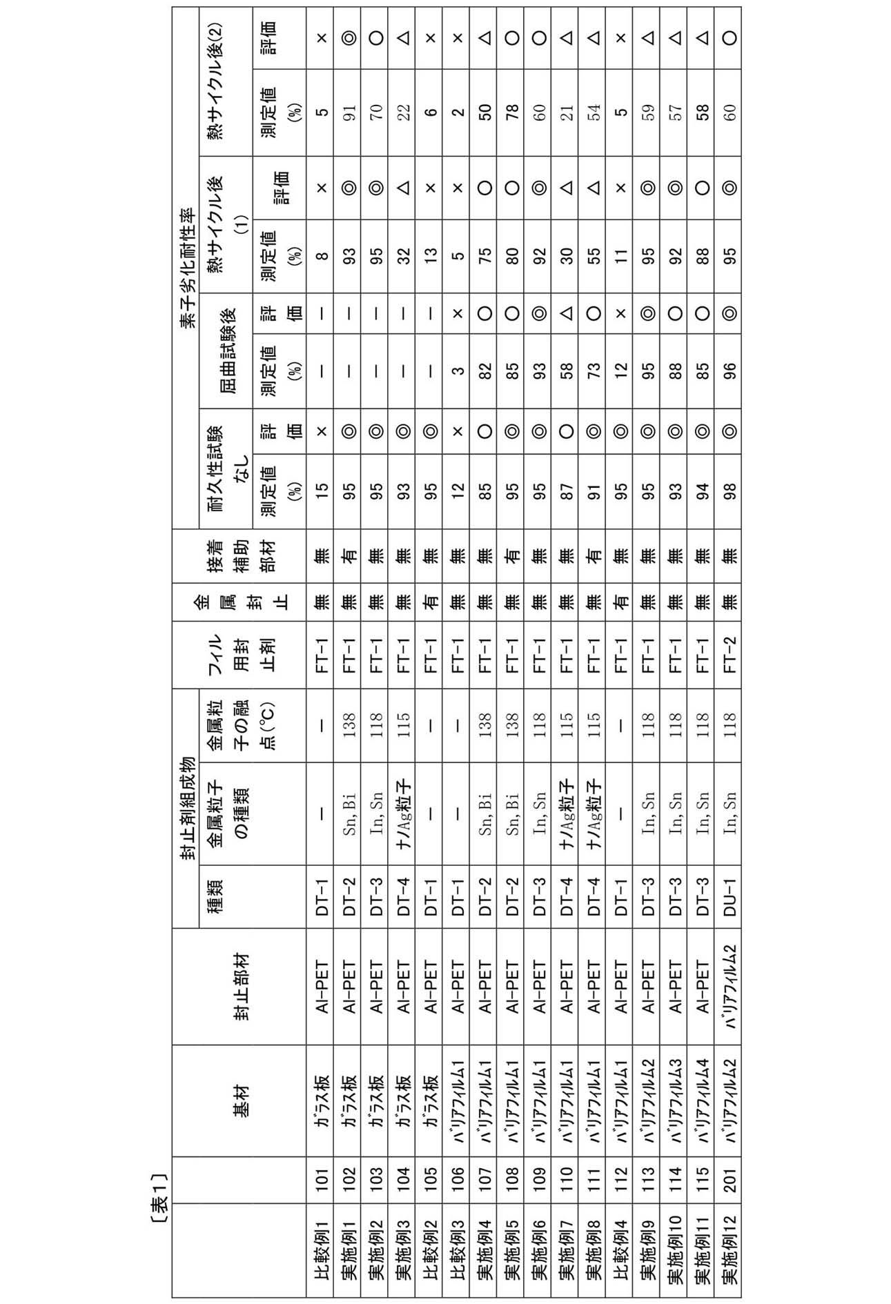
上記表1に記載の結果から明らかなように、本発明の電子デバイス102~104、107~111、113~115、および201(実施例1~12)は、比較例1~4の電子デバイスに比べて劣化処理後(耐久性試験未実施)の素子劣化耐性に優れ、更に各種の耐久性試験後に劣化処理した際の素子劣化耐性(耐久性)に優れることが分かる。詳しくは、耐久性試験として屈曲試験後、熱サイクル(1)後及び熱サイクル(2)後にそれぞれ劣化処理した後の素子劣化耐性(耐久性)においても優れることが分かる。さらに実施例1~12の電子デバイスのなかでも、金属粒子としてナノ金属粒子(ナノ銀粒子)のもの(実施例3、7、8)よりもマイクロサイズの各種はんだ粒子(SnとIn又はBi)を用いた方(実施例1、2、4~6、9~12)が、熱サイクル(1)後及び熱サイクル(2)後の素子劣化耐性(耐久性)に優れることがわかった。また、接着補助部材を用いていないもの(実施例4、7)よりも接着補助部材を用いた方(実施例5、8)が、劣化処理後(耐久性試験未実施)の素子劣化耐性率、屈曲試験後に劣化処理した後の素子劣化耐性率、および熱サイクル(1)後に劣化処理した後の素子劣化耐性率のいずれもが、3~15%程度改善されていることがわかった。また、接着補助部材を用いた方(実施例5、8)では、熱サイクル(1)後と熱サイクル(2)後の素子劣化耐性率の差が1~2%と非常に小さく、長期間にわたり熱サイクル劣化が大幅に抑制されていることがわかった。
また、実施例12の方法によれば、封止剤組成物のUV硬化処理を行うことにより、電子デバイスの熱履歴を少なくすることができる。
(実施例13)
ガスバリア性フィルム2のガスバリア層2の上に、第一の電極(陽極)としてインジウムスズ酸化物(ITO)透明導電膜を厚さ150nmで堆積したもの(シート抵抗12Ω/square)を、通常のフォトリソグラフィー法と湿式エッチングとを用いて10mm幅にパターニングし、第一の電極を形成した。パターン形成した第一の電極を、界面活性剤と超純水とによる超音波洗浄、超純水による超音波洗浄の順で洗浄後、窒素ブローで乾燥させ、最後に紫外線オゾン洗浄を行った。次いで、正孔輸送層として、導電性高分子およびポリアニオンからなるPEDOT-PSS(CLEVIOS(登録商標) P VP AI 4083、ヘレオス株式会社製、導電率:1×10⁻³S/cm)を2.0質量%で含むイソプロパノール溶液を調製し、乾燥膜厚が約30nmになるように、基板を65℃に調温したブレードコーターを用いて塗布乾燥した。その後、120℃の温風で20秒間加熱処理して、正孔輸送層を上記第一の電極上に製膜した。これ以降は、グローブボックス中に持ち込み、窒素雰囲気下で作業した。
ガスバリア性フィルム2のガスバリア層2の上に、第一の電極(陽極)としてインジウムスズ酸化物(ITO)透明導電膜を厚さ150nmで堆積したもの(シート抵抗12Ω/square)を、通常のフォトリソグラフィー法と湿式エッチングとを用いて10mm幅にパターニングし、第一の電極を形成した。パターン形成した第一の電極を、界面活性剤と超純水とによる超音波洗浄、超純水による超音波洗浄の順で洗浄後、窒素ブローで乾燥させ、最後に紫外線オゾン洗浄を行った。次いで、正孔輸送層として、導電性高分子およびポリアニオンからなるPEDOT-PSS(CLEVIOS(登録商標) P VP AI 4083、ヘレオス株式会社製、導電率:1×10⁻³S/cm)を2.0質量%で含むイソプロパノール溶液を調製し、乾燥膜厚が約30nmになるように、基板を65℃に調温したブレードコーターを用いて塗布乾燥した。その後、120℃の温風で20秒間加熱処理して、正孔輸送層を上記第一の電極上に製膜した。これ以降は、グローブボックス中に持ち込み、窒素雰囲気下で作業した。
まず、窒素雰囲気下で、上記正孔輸送層まで形成した素子を120℃で3分間加熱処理した。
次いで、o-ジクロロベンゼンに、p型有機半導体材料として下記化合物Aを0.8質量%、およびn型有機半導体材料であるPC60BM(フロンティアカーボン株式会社製、nanom(登録商標)spectra E100H)を1.6質量%混合した有機光電変換材料組成物溶液を調製した(p型有機半導体材料:n型有機半導体材料=33:67(質量比))。ホットプレートで100℃に加熱しながら攪拌(60分間)して完全に溶解した後、乾燥膜厚が約170nmになるように、基板を40℃に調温したブレードコーターを用いて塗布し、120℃で2分間乾燥して、光電変換層を上記正孔輸送層上に製膜した。
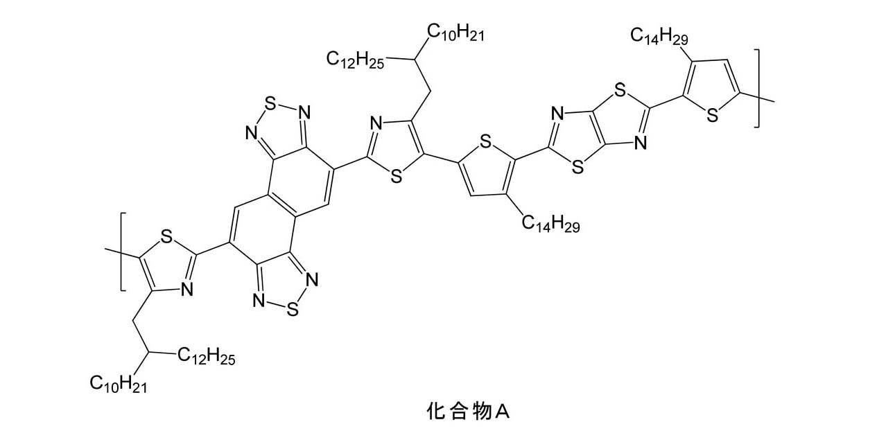

続いて、上記化合物Bを、0.02質量%の濃度になるように、1-ブタノール:ヘキサフルオロイソプロパノール=1:1の混合溶媒に溶解して溶液を調製した。この溶液を、乾燥膜厚が約5nmになるように、基板を65℃に調温したブレードコーターを用いて塗布乾燥した。その後、100℃の温風で2分間加熱処理して、電子輸送層を上記光電変換層上に製膜した。
次に、上記電子輸送層を製膜した素子を、真空蒸着装置内に設置した。そして、10mm幅のシャドウマスクが透明電極と直交するように素子をセットし、10-3Pa以下にまでに真空蒸着装置内を減圧した後、蒸着速度2nm/秒で銀を100nm蒸着して、第二の電極(陰極)を上記電子輸送層上に形成した。
図3に示すように、封止部材(符号12)として、30μm厚のアルミニウム箔(東洋アルミニウム株式会社製)に、ポリエチレンテレフタレート(PET)フィルム(12μm厚)を、ドライラミネーション用の接着剤(2液反応型のウレタン系接着剤)を用いドライラミネートしたもの(接着剤層の厚み1.5μm)を準備した。この封止部材(符号12)のアルミニウム箔上に、封止剤組成物DT-3(符号14’)を、武蔵エンジニアリング株式会社製ディスペンサーを使用し、ODF法により塗設した。塗設した大きさは45mm×45mm、直角部のR=1mmであった。フィル用封止剤FT-1(符号16)を、封止剤組成物DT-3(符号14’)の内側に等間隔で10×10か所に分けて滴下した。この封止部材(符号12)を、ランテクニカルサービス株式会社製真空貼り合わせ装置を使用し、封止剤層(封止剤組成物DT-3の塗膜)の厚さが20μmになるように、上記の保護層(符号15)を形成した電子素子本体(符号13)と貼り合わせ、160℃で5分間加熱し、封止剤組成物DT-3(符号14’)のはんだ粒子(符号14a)を溶融、凝集してはんだ相(符号14c)を形成すると共に、熱硬化型の液状エポキシ樹脂(図4の上図の符号14b)を熱硬化させてエポキシ樹脂(図4の下図の符号14b)を形成することで、封止剤組成物接合体DT-3(符号14)を形成し、封止を完了させ、電子デバイス(符号10)である有機光電変換素子301を得た。
<有機光電変換素子の評価>
耐久性試験前の試料A、上記の(黒点の評価:耐久性試験 屈曲試験)および(黒点の評価:耐久性試験 熱サイクル)と同様に屈曲試験を行った試料Bおよび熱サイクルを行った試料Cを、加速劣化処理として60℃、90%RHの環境で1000hr放置し、開放電圧、曲線因子、および光電変換効率を評価した。ここで、耐久性試験前の試料Aとは、有機光電変換素子301につき、加速劣化処理も耐久性試験も未実施の試料をいう。屈曲試験を行った試料Bとは、有機光電変換素子301につき、耐久性試験(屈曲試験)として、直径10cmの円柱に巻きつけて5分放置した後に平面上広げ5分放置する操作を100回行った試料をいう。熱サイクルを行った試料Cとは、有機光電変換素子301に対して、耐久性試験(熱サイクル)として、-40℃~85℃の熱サイクルを500回実施した試料をいう。
耐久性試験前の試料A、上記の(黒点の評価:耐久性試験 屈曲試験)および(黒点の評価:耐久性試験 熱サイクル)と同様に屈曲試験を行った試料Bおよび熱サイクルを行った試料Cを、加速劣化処理として60℃、90%RHの環境で1000hr放置し、開放電圧、曲線因子、および光電変換効率を評価した。ここで、耐久性試験前の試料Aとは、有機光電変換素子301につき、加速劣化処理も耐久性試験も未実施の試料をいう。屈曲試験を行った試料Bとは、有機光電変換素子301につき、耐久性試験(屈曲試験)として、直径10cmの円柱に巻きつけて5分放置した後に平面上広げ5分放置する操作を100回行った試料をいう。熱サイクルを行った試料Cとは、有機光電変換素子301に対して、耐久性試験(熱サイクル)として、-40℃~85℃の熱サイクルを500回実施した試料をいう。
〈短絡電流密度、開放電圧、曲線因子、および光電変換効率の測定〉
作製した有機光電変換素子を、ソーラーシミュレーター(AM1.5Gフィルタ)を用いて100mW/cm2の強度の光を照射し、有効面積を1cm2にしたマスクを受光部に重ね、IV特性を評価することで、短絡電流密度Jsc(mA/cm2)、開放電圧Voc(V)、および曲線因子FFを測定し、さらに光電変換効率を下記式により算出した。評価結果を下記表2に示す。
作製した有機光電変換素子を、ソーラーシミュレーター(AM1.5Gフィルタ)を用いて100mW/cm2の強度の光を照射し、有効面積を1cm2にしたマスクを受光部に重ね、IV特性を評価することで、短絡電流密度Jsc(mA/cm2)、開放電圧Voc(V)、および曲線因子FFを測定し、さらに光電変換効率を下記式により算出した。評価結果を下記表2に示す。


上記表2から明らかなように、実施例13の有機光電変換素子301は、耐久性評価での性能劣化は見られず、良好な封止性能が得られることが確認できた。即ち、耐久性試験前の試料Aと、耐久性試験(屈曲試験)後の試料B及び耐久性試験(熱サイクル)後の試料Cとの間で、加速劣化処理する前の短絡電流密度、開放電圧、曲線因子および光電変換効率に優位差は認められなかった。同様に、試料Aと、試料B及びCとの間で、加速劣化処理後の短絡電流密度、開放電圧、曲線因子および光電変換効率にも優位差は認められなかった。さらに各試料ごとの加速劣化処理前と加速劣化処理後での短絡電流密度、開放電圧、曲線因子および光電変換効率にも優位差は認められず、加速劣化処理による性能劣化も認められなかった。以上のことから、良好な封止性能が得られることが確認できた。
1 支持体(ア)上に無機層を形成した積層フィルム、
2 支持体(ア)、
3 酸素含有炭化ケイ素からなる無機層、
10 電子デバイス、
11 基材、
12 封止部材、
13 電子素子本体、
14 封止剤組成物、
14a 金属粒子、
14b 樹脂、
14c 金属相、
15 保護層、
16 フィル用封止剤、
17 第1電極(陽極)、
18 正孔輸送層、
19 発光層、
20 電子輸送層、
21 第2電極(陰極)、
30 接着補助部材、
31 製造装置、
32 送り出しローラー、
33、34、35、36 搬送ローラー、
39、40 成膜ローラー、
41 ガス供給管、
42 プラズマ発生用電源、
43、44 磁場発生装置、
45 巻取りローラー。
2 支持体(ア)、
3 酸素含有炭化ケイ素からなる無機層、
10 電子デバイス、
11 基材、
12 封止部材、
13 電子素子本体、
14 封止剤組成物、
14a 金属粒子、
14b 樹脂、
14c 金属相、
15 保護層、
16 フィル用封止剤、
17 第1電極(陽極)、
18 正孔輸送層、
19 発光層、
20 電子輸送層、
21 第2電極(陰極)、
30 接着補助部材、
31 製造装置、
32 送り出しローラー、
33、34、35、36 搬送ローラー、
39、40 成膜ローラー、
41 ガス供給管、
42 プラズマ発生用電源、
43、44 磁場発生装置、
45 巻取りローラー。
Claims (6)
- 基材と、
封止部材と、
前記基材と前記封止部材との間に位置する、電子素子本体と、
金属単体または合金を含む金属および樹脂を含む封止剤組成物接合体と、
を含み、
前記基材と前記封止部材とが、前記封止剤組成物接合体を介して接合されることにより、前記電子素子本体が封止されてなる、電子デバイス。 - 前記金属の融点は、80~200℃である、請求項1に記載の電子デバイス。
- 前記金属は、錫と、インジウムおよびビスマスの少なくとも一方と、を含む、請求項1または2に記載の電子デバイス。
- 前記基材および前記封止部材の少なくとも一方は、前記基材と前記封止部材との接着を補助し、前記封止剤組成物接合体に当接し、かつ金属からなる接着補助部材を有する、請求項1~3のいずれか1項に記載の電子デバイス。
- 基材と、
封止部材と、
前記基材と前記封止部材との間に位置する電子素子本体と、
金属単体または合金を含む金属および樹脂を含む封止剤組成物接合体と、
を含む、電子デバイスの製造方法であって、
前記基材上に電子素子本体を配置する工程と、
前記封止部材上に前記封止剤組成物接合体形成用原料である、金属単体または合金を含む金属粒子および樹脂を含む封止剤組成物を塗布する工程と、
前記基材および前記電子素子本体を覆うように、前記封止剤組成物が塗布された前記封止部材を配置する工程と、
前記封止剤組成物中の前記金属粒子を溶融し、前記基材および前記封止部材と結着する金属相を形成する工程と、
前記封止剤組成物中の樹脂を硬化させ、前記封止剤組成物接合体を形成する工程と、
を含む、電子デバイスの製造方法。 - 外部エネルギーにより硬化し、電子デバイスの封止に用いられる封止剤組成物であって、
金属単体または合金を含む金属粒子と、樹脂とを含み、
前記封止剤組成物のうち前記金属粒子を除いたときの封止剤組成物の、前記封止剤組成物に内包される前記金属粒子の融点で1分間放置した後の粘度が1Pa・s以下であり、かつ硬化前の25℃における粘度が100~1000Pa・sである、電子デバイス用封止剤組成物。
Priority Applications (1)
| Application Number | Priority Date | Filing Date | Title |
|---|---|---|---|
| JP2014522718A JPWO2014003196A1 (ja) | 2012-06-29 | 2013-07-01 | 電子デバイスおよびその製造方法 |
Applications Claiming Priority (2)
| Application Number | Priority Date | Filing Date | Title |
|---|---|---|---|
| JP2012147575 | 2012-06-29 | ||
| JP2012-147575 | 2012-06-29 |
Publications (1)
| Publication Number | Publication Date |
|---|---|
| WO2014003196A1 true WO2014003196A1 (ja) | 2014-01-03 |
Family
ID=49783329
Family Applications (1)
| Application Number | Title | Priority Date | Filing Date |
|---|---|---|---|
| PCT/JP2013/068057 Ceased WO2014003196A1 (ja) | 2012-06-29 | 2013-07-01 | 電子デバイスおよびその製造方法 |
Country Status (2)
| Country | Link |
|---|---|
| JP (1) | JPWO2014003196A1 (ja) |
| WO (1) | WO2014003196A1 (ja) |
Cited By (5)
| Publication number | Priority date | Publication date | Assignee | Title |
|---|---|---|---|---|
| CN107104201A (zh) * | 2017-05-25 | 2017-08-29 | 京东方科技集团股份有限公司 | 一种有机发光二极管显示面板封装结构及其制作方法、显示装置 |
| WO2018235596A1 (ja) * | 2017-06-19 | 2018-12-27 | 株式会社ブイ・テクノロジー | 表示装置 |
| WO2020205917A1 (en) * | 2019-04-01 | 2020-10-08 | First Solar, Inc. | Photovoltaic devices with encapsulation layers and systems and methods for forming the same |
| FR3131082A1 (fr) * | 2021-12-21 | 2023-06-23 | Commissariat A L'energie Atomique Et Aux Energies Alternatives | Module photovoltaïque doté d’une couche barrière à la perméation d’H2O gazeux |
| EP4318697A4 (en) * | 2021-12-06 | 2025-06-04 | Lg Energy Solution, Ltd. | Electrode arrangement, manufacturing method therefor and battery cell therewith |
Citations (6)
| Publication number | Priority date | Publication date | Assignee | Title |
|---|---|---|---|---|
| JP2004265837A (ja) * | 2003-03-04 | 2004-09-24 | Seiko Epson Corp | 表示パネル及びその表示パネルを備えた電子機器並びに表示パネル及びその表示パネルを備えた電子機器の製造方法 |
| JP2005285732A (ja) * | 2003-12-16 | 2005-10-13 | Dainippon Printing Co Ltd | 有機機能素子およびその製造方法 |
| JP2007048674A (ja) * | 2005-08-11 | 2007-02-22 | Ngk Spark Plug Co Ltd | 色素増感型太陽電池及びその封止方法 |
| JP2008251242A (ja) * | 2007-03-29 | 2008-10-16 | Fujifilm Corp | 電子デバイスおよびその製造方法 |
| JP2008249839A (ja) * | 2007-03-29 | 2008-10-16 | Fujifilm Corp | 有機elパネルおよびその製造方法 |
| JP2009545113A (ja) * | 2006-07-28 | 2009-12-17 | サン−ゴバン グラス フランス | 封入発光素子 |
-
2013
- 2013-07-01 WO PCT/JP2013/068057 patent/WO2014003196A1/ja not_active Ceased
- 2013-07-01 JP JP2014522718A patent/JPWO2014003196A1/ja not_active Withdrawn
Patent Citations (6)
| Publication number | Priority date | Publication date | Assignee | Title |
|---|---|---|---|---|
| JP2004265837A (ja) * | 2003-03-04 | 2004-09-24 | Seiko Epson Corp | 表示パネル及びその表示パネルを備えた電子機器並びに表示パネル及びその表示パネルを備えた電子機器の製造方法 |
| JP2005285732A (ja) * | 2003-12-16 | 2005-10-13 | Dainippon Printing Co Ltd | 有機機能素子およびその製造方法 |
| JP2007048674A (ja) * | 2005-08-11 | 2007-02-22 | Ngk Spark Plug Co Ltd | 色素増感型太陽電池及びその封止方法 |
| JP2009545113A (ja) * | 2006-07-28 | 2009-12-17 | サン−ゴバン グラス フランス | 封入発光素子 |
| JP2008251242A (ja) * | 2007-03-29 | 2008-10-16 | Fujifilm Corp | 電子デバイスおよびその製造方法 |
| JP2008249839A (ja) * | 2007-03-29 | 2008-10-16 | Fujifilm Corp | 有機elパネルおよびその製造方法 |
Cited By (7)
| Publication number | Priority date | Publication date | Assignee | Title |
|---|---|---|---|---|
| CN107104201A (zh) * | 2017-05-25 | 2017-08-29 | 京东方科技集团股份有限公司 | 一种有机发光二极管显示面板封装结构及其制作方法、显示装置 |
| US10923676B2 (en) | 2017-05-25 | 2021-02-16 | Hefei Boe Optoelectronics Technology Co., Ltd. | Encapsulating structure of organic light emitting diode display panel having concave-convex structure in encapsulating portion |
| WO2018235596A1 (ja) * | 2017-06-19 | 2018-12-27 | 株式会社ブイ・テクノロジー | 表示装置 |
| WO2020205917A1 (en) * | 2019-04-01 | 2020-10-08 | First Solar, Inc. | Photovoltaic devices with encapsulation layers and systems and methods for forming the same |
| EP4318697A4 (en) * | 2021-12-06 | 2025-06-04 | Lg Energy Solution, Ltd. | Electrode arrangement, manufacturing method therefor and battery cell therewith |
| FR3131082A1 (fr) * | 2021-12-21 | 2023-06-23 | Commissariat A L'energie Atomique Et Aux Energies Alternatives | Module photovoltaïque doté d’une couche barrière à la perméation d’H2O gazeux |
| EP4203074A1 (fr) * | 2021-12-21 | 2023-06-28 | Commissariat à l'Energie Atomique et aux Energies Alternatives | Module photovoltaïque doté d'une couche barrière à la perméation d h2o gazeux |
Also Published As
| Publication number | Publication date |
|---|---|
| JPWO2014003196A1 (ja) | 2016-06-02 |
Similar Documents
| Publication | Publication Date | Title |
|---|---|---|
| JP5716752B2 (ja) | ガスバリアフィルムの製造方法、ガスバリアフィルムおよび電子デバイス | |
| JP5888329B2 (ja) | ガスバリア性フィルム、ガスバリア性フィルムの製造方法、および電子デバイス | |
| JP5821637B2 (ja) | ガスバリアフィルム、ガスバリアフィルムの製造方法及び有機光電変換素子 | |
| JP5691175B2 (ja) | ガスバリアフィルムの製造方法、ガスバリアフィルム及び有機光電変換素子 | |
| JP5835344B2 (ja) | ガスバリアーフィルム及び電子機器 | |
| JP5712509B2 (ja) | バリアフィルムの製造方法 | |
| JP5540803B2 (ja) | ガスバリア性フィルムの製造方法 | |
| WO2014003196A1 (ja) | 電子デバイスおよびその製造方法 | |
| JP5935263B2 (ja) | ガスバリア性フィルム、ガスバリア性フィルムの製造方法、及びガスバリア性フィルムを有する有機電子デバイス | |
| JP2012076385A (ja) | ガスバリア性フィルム、ガスバリア性フィルムの製造方法、及び該ガスバリア性フィルムを有する有機電子デバイス | |
| WO2016133130A1 (ja) | 封止構造体 | |
| JP2012000599A (ja) | バリアフィルム及びその製造方法、有機電子デバイス及びその製造方法 | |
| JP5692230B2 (ja) | ガスバリアフィルムの製造方法 | |
| JP2016187021A (ja) | 光電変換素子 | |
| JP5640976B2 (ja) | ガスバリアフィルムとその製造方法、これを用いた光電変換素子 | |
| JP2014056884A (ja) | 電子デバイスおよびその製造方法 | |
| JP2012116960A (ja) | ガスバリア性フィルム、その製造方法及び有機電子デバイス | |
| JP5600981B2 (ja) | ガスバリア性フィルム、有機デバイスの製造方法、および有機デバイス | |
| JP2011073417A (ja) | バリアフィルム、バリアフィルムの製造方法及び有機光電変換素子 | |
| JP5594099B2 (ja) | ガスバリア性フィルムの製造方法 | |
| EP4494431A1 (en) | Photoelectric conversion element, photoelectric conversion module, electronic device, and solar cell module | |
| JP6303835B2 (ja) | 電子デバイス | |
| JP2010027764A (ja) | 有機薄膜太陽電池 |
Legal Events
| Date | Code | Title | Description |
|---|---|---|---|
| 121 | Ep: the epo has been informed by wipo that ep was designated in this application |
Ref document number: 13809233 Country of ref document: EP Kind code of ref document: A1 |
|
| ENP | Entry into the national phase |
Ref document number: 2014522718 Country of ref document: JP Kind code of ref document: A |
|
| NENP | Non-entry into the national phase |
Ref country code: DE |
|
| 122 | Ep: pct application non-entry in european phase |
Ref document number: 13809233 Country of ref document: EP Kind code of ref document: A1 |