WO2014002855A1 - 表示装置及びテレビジョン受信機 - Google Patents
表示装置及びテレビジョン受信機 Download PDFInfo
- Publication number
- WO2014002855A1 WO2014002855A1 PCT/JP2013/066903 JP2013066903W WO2014002855A1 WO 2014002855 A1 WO2014002855 A1 WO 2014002855A1 JP 2013066903 W JP2013066903 W JP 2013066903W WO 2014002855 A1 WO2014002855 A1 WO 2014002855A1
- Authority
- WO
- WIPO (PCT)
- Prior art keywords
- display device
- backlight chassis
- display
- light
- display panel
- Prior art date
- Legal status (The legal status is an assumption and is not a legal conclusion. Google has not performed a legal analysis and makes no representation as to the accuracy of the status listed.)
- Ceased
Links
Images

Classifications
-
- H—ELECTRICITY
- H04—ELECTRIC COMMUNICATION TECHNIQUE
- H04N—PICTORIAL COMMUNICATION, e.g. TELEVISION
- H04N5/00—Details of television systems
- H04N5/64—Constructional details of receivers, e.g. cabinets or dust covers
-
- G—PHYSICS
- G02—OPTICS
- G02B—OPTICAL ELEMENTS, SYSTEMS OR APPARATUS
- G02B6/00—Light guides; Structural details of arrangements comprising light guides and other optical elements, e.g. couplings
- G02B6/0001—Light guides; Structural details of arrangements comprising light guides and other optical elements, e.g. couplings specially adapted for lighting devices or systems
- G02B6/0011—Light guides; Structural details of arrangements comprising light guides and other optical elements, e.g. couplings specially adapted for lighting devices or systems the light guides being planar or of plate-like form
- G02B6/0081—Mechanical or electrical aspects of the light guide and light source in the lighting device peculiar to the adaptation to planar light guides, e.g. concerning packaging
- G02B6/0083—Details of electrical connections of light sources to drivers, circuit boards, or the like
-
- G—PHYSICS
- G02—OPTICS
- G02B—OPTICAL ELEMENTS, SYSTEMS OR APPARATUS
- G02B6/00—Light guides; Structural details of arrangements comprising light guides and other optical elements, e.g. couplings
- G02B6/0001—Light guides; Structural details of arrangements comprising light guides and other optical elements, e.g. couplings specially adapted for lighting devices or systems
- G02B6/0011—Light guides; Structural details of arrangements comprising light guides and other optical elements, e.g. couplings specially adapted for lighting devices or systems the light guides being planar or of plate-like form
- G02B6/0081—Mechanical or electrical aspects of the light guide and light source in the lighting device peculiar to the adaptation to planar light guides, e.g. concerning packaging
- G02B6/0086—Positioning aspects
- G02B6/009—Positioning aspects of the light source in the package
-
- G—PHYSICS
- G02—OPTICS
- G02F—OPTICAL DEVICES OR ARRANGEMENTS FOR THE CONTROL OF LIGHT BY MODIFICATION OF THE OPTICAL PROPERTIES OF THE MEDIA OF THE ELEMENTS INVOLVED THEREIN; NON-LINEAR OPTICS; FREQUENCY-CHANGING OF LIGHT; OPTICAL LOGIC ELEMENTS; OPTICAL ANALOGUE/DIGITAL CONVERTERS
- G02F1/00—Devices or arrangements for the control of the intensity, colour, phase, polarisation or direction of light arriving from an independent light source, e.g. switching, gating or modulating; Non-linear optics
- G02F1/01—Devices or arrangements for the control of the intensity, colour, phase, polarisation or direction of light arriving from an independent light source, e.g. switching, gating or modulating; Non-linear optics for the control of the intensity, phase, polarisation or colour
- G02F1/13—Devices or arrangements for the control of the intensity, colour, phase, polarisation or direction of light arriving from an independent light source, e.g. switching, gating or modulating; Non-linear optics for the control of the intensity, phase, polarisation or colour based on liquid crystals, e.g. single liquid crystal display cells
- G02F1/133—Constructional arrangements; Operation of liquid crystal cells; Circuit arrangements
- G02F1/13306—Circuit arrangements or driving methods for the control of single liquid crystal cells
-
- G—PHYSICS
- G02—OPTICS
- G02F—OPTICAL DEVICES OR ARRANGEMENTS FOR THE CONTROL OF LIGHT BY MODIFICATION OF THE OPTICAL PROPERTIES OF THE MEDIA OF THE ELEMENTS INVOLVED THEREIN; NON-LINEAR OPTICS; FREQUENCY-CHANGING OF LIGHT; OPTICAL LOGIC ELEMENTS; OPTICAL ANALOGUE/DIGITAL CONVERTERS
- G02F1/00—Devices or arrangements for the control of the intensity, colour, phase, polarisation or direction of light arriving from an independent light source, e.g. switching, gating or modulating; Non-linear optics
- G02F1/01—Devices or arrangements for the control of the intensity, colour, phase, polarisation or direction of light arriving from an independent light source, e.g. switching, gating or modulating; Non-linear optics for the control of the intensity, phase, polarisation or colour
- G02F1/13—Devices or arrangements for the control of the intensity, colour, phase, polarisation or direction of light arriving from an independent light source, e.g. switching, gating or modulating; Non-linear optics for the control of the intensity, phase, polarisation or colour based on liquid crystals, e.g. single liquid crystal display cells
- G02F1/133—Constructional arrangements; Operation of liquid crystal cells; Circuit arrangements
- G02F1/1333—Constructional arrangements; Manufacturing methods
- G02F1/133308—Support structures for LCD panels, e.g. frames or bezels
-
- H—ELECTRICITY
- H04—ELECTRIC COMMUNICATION TECHNIQUE
- H04N—PICTORIAL COMMUNICATION, e.g. TELEVISION
- H04N5/00—Details of television systems
- H04N5/44—Receiver circuitry for the reception of television signals according to analogue transmission standards
-
- H—ELECTRICITY
- H04—ELECTRIC COMMUNICATION TECHNIQUE
- H04N—PICTORIAL COMMUNICATION, e.g. TELEVISION
- H04N5/00—Details of television systems
- H04N5/64—Constructional details of receivers, e.g. cabinets or dust covers
- H04N5/655—Construction or mounting of chassis, e.g. for varying the elevation of the tube
-
- G—PHYSICS
- G02—OPTICS
- G02B—OPTICAL ELEMENTS, SYSTEMS OR APPARATUS
- G02B6/00—Light guides; Structural details of arrangements comprising light guides and other optical elements, e.g. couplings
- G02B6/0001—Light guides; Structural details of arrangements comprising light guides and other optical elements, e.g. couplings specially adapted for lighting devices or systems
- G02B6/0011—Light guides; Structural details of arrangements comprising light guides and other optical elements, e.g. couplings specially adapted for lighting devices or systems the light guides being planar or of plate-like form
- G02B6/0081—Mechanical or electrical aspects of the light guide and light source in the lighting device peculiar to the adaptation to planar light guides, e.g. concerning packaging
-
- G—PHYSICS
- G02—OPTICS
- G02F—OPTICAL DEVICES OR ARRANGEMENTS FOR THE CONTROL OF LIGHT BY MODIFICATION OF THE OPTICAL PROPERTIES OF THE MEDIA OF THE ELEMENTS INVOLVED THEREIN; NON-LINEAR OPTICS; FREQUENCY-CHANGING OF LIGHT; OPTICAL LOGIC ELEMENTS; OPTICAL ANALOGUE/DIGITAL CONVERTERS
- G02F1/00—Devices or arrangements for the control of the intensity, colour, phase, polarisation or direction of light arriving from an independent light source, e.g. switching, gating or modulating; Non-linear optics
- G02F1/01—Devices or arrangements for the control of the intensity, colour, phase, polarisation or direction of light arriving from an independent light source, e.g. switching, gating or modulating; Non-linear optics for the control of the intensity, phase, polarisation or colour
- G02F1/13—Devices or arrangements for the control of the intensity, colour, phase, polarisation or direction of light arriving from an independent light source, e.g. switching, gating or modulating; Non-linear optics for the control of the intensity, phase, polarisation or colour based on liquid crystals, e.g. single liquid crystal display cells
- G02F1/133—Constructional arrangements; Operation of liquid crystal cells; Circuit arrangements
- G02F1/1333—Constructional arrangements; Manufacturing methods
- G02F1/133308—Support structures for LCD panels, e.g. frames or bezels
- G02F1/133314—Back frames
Definitions
- the present invention relates to a display device for displaying an image and a television receiver.
- a television receiver including a liquid crystal display device that displays an image on a liquid crystal panel is widely used as a display device (see Patent Document 1).
- the display device included in the television receiver described in Patent Document 1 has a backlight (light source unit) that emits light toward one surface of a liquid crystal panel (display panel), and the light source unit has a box shape. It is supported on the bottom wall of the backlight chassis. The entire outside of the backlight chassis is covered with a back cover.
- a display device in which a backlight chassis constitutes a part of an outline can be considered. This display device is thin and light because the back cover does not cover the backlight chassis.
- the rigidity of the display device is low. Therefore, it is necessary to increase the rigidity of the backlight chassis so that the display device has sufficient rigidity so that the display device does not deform due to an impact assumed during use.
- the backlight chassis constitutes a part of the outline of the display device, it is necessary to increase the rigidity of the backlight chassis without impairing the appearance. For this reason, it is not preferable to increase the rigidity of the backlight chassis by attaching metal fittings or attaching a diaphragm to the bottom wall of the backlight chassis, because the appearance of the display device is impaired.
- the present invention has been made in view of such circumstances, and an object of the present invention is to provide a thin and light display device and a television receiver capable of improving the appearance of the backlight chassis with high rigidity. There is to do.
- the display device is a display device in which a backlight chassis that supports a light source unit that emits light for displaying an image forms a part of an outer shell, and the backlight chassis includes the light source It has a peripheral wall that surrounds the unit and is connected continuously.
- the backlight chassis that supports the light source unit that emits light for displaying an image and forms a part of the outer shell has a peripheral wall that is integrally connected, and the peripheral wall Surrounds the light source unit.
- the backlight chassis Since the integrally connected peripheral walls function as ribs to the bottom wall of the backlight chassis, the backlight chassis has high rigidity, particularly with respect to twisting force. Accordingly, it is not necessary to attach a metal fitting or a diaphragm to a portion constituting a part of the outer wall such as the bottom wall and the peripheral wall of the backlight chassis, so that the appearance can be improved. Further, since there is no member covering the entire backlight chassis, the thickness is thin and the weight is light.
- the display device according to the present invention is characterized in that a cutout is provided in the peripheral wall.
- the backlight chassis is provided with a notch in the peripheral wall. Therefore, for example, an FPC (Flexible Printed Circuit) that connects a display panel that displays an image and a control circuit that controls display of the image on the display panel can be arranged in a notch, and wiring of the FPC can be easily performed.
- FPC Flexible Printed Circuit
- the display device is characterized in that the backlight chassis further supports a display panel for displaying the image, overlapping the light source unit.
- the thickness is thinner.
- a television receiver includes the above-described display device and a receiving unit that receives a television broadcast, and displays an image on the display device based on the television broadcast received by the receiving unit. It is characterized by that.
- the backlight chassis of the display device since the image is displayed on the aforementioned display device based on the television broadcast received by the receiver, the backlight chassis of the display device has high rigidity. Accordingly, it is not necessary to attach a metal fitting or a diaphragm to a portion constituting a part of the outer wall such as the bottom wall and the peripheral wall of the backlight chassis, so that the appearance can be improved. Further, since there is no member covering the entire backlight chassis, the thickness is thin and the weight is light.
- the backlight chassis surrounds the light source unit and has a peripheral wall that is integrally connected, the backlight chassis has high rigidity and a thin and light display device and television that can have a good appearance. John receiver can be realized.
- FIG. 3 is a schematic cross-sectional view of the display device taken along line BB in FIG. 2. It is a schematic sectional drawing of the display apparatus cut
- FIG. 1 is a schematic diagram showing the appearance of a television receiver according to the present invention.
- the television receiver 1 includes a display device 10, a receiving unit 11, a signal processing unit 12, and a stand 13.
- the display device 10 includes a rectangular plate-like display panel 22 for displaying an image, and the peripheral edge of the display panel 22 is covered with a rectangular frame-like cover 23 having an opening 23a at the center.
- a rectangular frame-like cover 23 having an opening 23a at the center.
- an effective display area located at the center of the display surface for displaying an image is exposed from the opening 23a.
- the vertical and horizontal dimensions of the opening 23 a are slightly smaller than the vertical and horizontal dimensions of the display panel 22 so that the cover 23 can cover the periphery of the display panel 22.
- the backlight chassis 21 supports a later-described light source unit that emits light to the opposite surface, and constitutes a part of the outline of the display device 10.
- the receiving unit 11 is connected to an antenna (not shown) and receives a television broadcast via the antenna.
- the signal processing unit 12 demodulates data related to television broadcasting received by the receiving unit 11, separates image data from the demodulated data, and outputs the separated image data.
- the display panel 22 displays an image based on the image data output from the signal processing unit 12 on the display surface exposed from the opening 23 a of the cover 23.
- the stand 13 is provided outside the backlight chassis 21 and supports the display device 10 in a vertical posture.
- the side on which the display panel 22 is disposed is the front side, and the opposite side is the back side.
- the side on which the stand 13 is arranged in the television receiver 1 is the lower side of the display device 10, and the opposite side is the upper side of the display device 10.
- the right and left sides of the display panel 22 viewed from the outside of the display panel 22 exposed from the opening 23 a of the cover 23 are the right side and the left side of the display device 10, respectively.
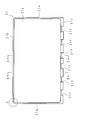
- FIG. 2 is a front view of the backlight chassis 21.
- the backlight chassis 21 has a box shape with one open surface, and a plurality of side walls 21b, 21c, 21d, and 21e are erected from each side of a rectangular plate-shaped bottom wall 21a.
- the side walls 21b, 21c, 21d, and 21e have substantially the same height and thickness.
- the backlight chassis 21 is disposed such that the side walls 21 b, 21 c, 21 d, and 21 e are on the upper side, the lower side, the left side, and the right side of the display device 10.
- the backlight chassis 21 is manufactured by, for example, press working of an aluminum plate, and the side walls 21b, 21c, 21d, and 21e are integrally connected peripheral walls. A portion shown in FIG. 2 indicates a connecting portion of the side walls 21b and 21d.
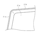
- FIG. 3 is a perspective view of the backlight chassis 21 in which the portion A of FIG. 2 is enlarged.
- the side walls 21b and 21d are continuous, and the connecting portion of the side walls 21b and 21d is curved in an arc shape.
- the connecting portions of the side walls 21b and 21d are curved in an arc shape.
- rectangular cutouts 21f, 21f,..., 21f formed by cutting out the edge of the side wall 21c at an appropriate length are provided on the side wall 21c at appropriate intervals.
- FPCs 29, 29,..., 29 described later are provided at the lower side of the display panel 22 with similar intervals. Arranged.
- each of the bottom wall 21a and the side walls 21b, 21c, 21d, and 21e is appropriately set within a range of, for example, 1 to 1.2 mm, and the depth from the open surface of the backlight chassis 21 to the bottom wall 21a is For example, it is appropriately set in the range of 5 to 6 mm.
- the backlight chassis 21 configured as described above has a peripheral wall in which the side walls 21b, 21c, 21d, and 21e are integrally connected. Since the peripheral wall functions as a rib with respect to the bottom wall 21 a, the rigidity of the backlight chassis 21, particularly the rigidity against a twisting force is high. Accordingly, the backlight chassis 21 is provided with a metal fitting or a diaphragm attached to a part of the outline of the display device 10, that is, the back surface of the bottom wall 21a and the outer surfaces of the side walls 21b, 21c, 21d, and 21e. It is not necessary to increase the rigidity of the backlight chassis 21 and the appearance of the display device 10 can be improved.
- the display device 10 and the television receiver 1 including the display device 10 are thin and light. It is possible to meet the demand for narrowing the cover 23 that covers from the outside of the backlight chassis 21.
- the backlight chassis 21 is easily manufactured when it is a pressed product of an aluminum plate. Further, since the connecting portion of the side walls 21b and 21e, the connecting portion of the side walls 21c and 21e, the connecting portion of the side walls 21c and 21d, and the connecting portion of the side walls 21c and 21d are curved in an arc shape, the backlight chassis 21 Is more easily manufactured.
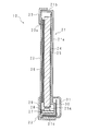
- FIG. 4 is a schematic cross-sectional view of the display device 10 cut along the line BB in FIG. 2
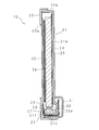
- FIG. 5 is a schematic cross-sectional view of the display device 10 cut along the line CC in FIG.
- the backlight chassis 21 supports the display panel 22, the reflection sheet 24, the light guide plate 25, and the optical sheet group 26 in a stacked manner.
- the peripheral portion of the display surface of the display panel 22 and the peripheral surface of the display panel 22 are covered from the outside of the backlight chassis 21 by the cover 23.
- a rectangular plate-shaped LED (Light Emitting Diode) substrate 27 is disposed so that the longitudinal direction thereof coincides with the left-right direction of the display device 10.
- LEDs 28, 28,..., 28 are disposed at appropriate intervals along the longitudinal direction of the LED board 27.
- the LEDs 28, 28,..., 28 each emit light toward the lower end surface 25 a of the light guide plate 25 in the directions indicated by the arrows in FIGS.
- a peripheral wall composed of the side walls 21b, 21c, 21d, and 21e surrounds the display panel 22, the reflection sheet 24, the light guide plate 25, the optical sheet group 26, the LED substrate 27, and the LEDs 28, 28,.
- the light guide plate 25 is made of, for example, acrylic resin.
- the light emitted from each of the LEDs 28, 28,..., 28 enters the light guide plate 25 from the lower end surface 25a, and is repeatedly reflected on the front and back surfaces of the light guide plate 25.
- part of the light is emitted toward the optical sheet group 26.
- the back surface of the light guide plate 25 is in close contact with the reflection sheet 24, all light propagating through the light guide plate 25 is reflected on the back surface. Thereby, the light guide plate 25 emits uniform light from the front toward the optical sheet group 26.
- the vertical and horizontal dimensions of the reflection sheet 24 are larger than the vertical and horizontal dimensions of the back surface of the light guide plate 25, and the reflection sheet 24 completely covers the back surface of the light guide plate 25. Will not leak.
- the light emitted from the front surface of the light guide plate 25 passes through the optical sheet group 26 and is irradiated on the back surface of the display panel 22.
- the optical sheet group 26 is disposed in close contact with the back surface of the display panel 22 and the front surface of the light guide plate 25, and has an optical sheet having a diffusion function for diffusing light, and a light collecting function for condensing light.
- a plurality of optical sheets, such as an optical sheet, are laminated.
- the optical sheet group 26 collects and diffuses light transmitted through the optical sheet group 26.
- the display panel 22 has a glass plate on the display surface side and a glass plate on the back side. Liquid crystal is disposed between the two glass plates, and the transmittance of light transmitted through the display panel 22 changes according to the voltage applied to the liquid crystal. Thereby, the display panel 22 transmits or blocks light incident from the back surface. As a result, an image is displayed on the display surface of the display panel 22.
- the reflection sheet 24, the light guide plate 25, the LED substrate 27, and the LEDs 28, 28,..., 28 function as a light source unit that emits light for displaying an image. Furthermore, since the display panel 22 overlaps with the light guide plate 25 and the optical sheet group 26, the display device 10 is thinner.
- FPCs 29, 29,..., 29 are notches 21f, 21f, in the lower side of the display panel 22, rectangular FPCs 29, 29,..., 29 (only one is shown in FIGS. 4 and 5) are notches 21f, 21f,.
- the FPCs 29, 29,... 29 are connected to the display panel 22 at one end.
- Each of the FPCs 29, 29,..., 29 hangs down from the lower side of the display panel 22 and is bent to the rear side while being passed through the notches 21f, 21f,. ,..., 29 are connected at the other end to a control circuit 30 disposed below the rear surface of the backlight chassis 21.
- the cutouts 21f, 21f,..., 21f are provided in the side wall 21c, so that the wiring of the FPCs 29, 29,. .
- Each of the FPCs 29, 29,..., 29 is provided with a drive circuit (not shown) that drives the display panel 22 by applying a voltage to the liquid crystal, and each drive circuit displays according to instructions from the control circuit 30. A voltage is applied to the liquid crystal of the panel 22.
- the control circuit 30 instructs the voltage applied to the liquid crystal by each drive circuit based on the image data output from the signal processing unit 12. Thereby, the transmittance of light transmitted through the display panel 22 changes based on the image data output from the signal processing unit 12, and an image based on the image data is displayed on the display surface of the display panel 22.
- a part of each of the FPCs 29, 29,..., 29 on the lower side of the backlight chassis 21 and the control circuit 30 are covered with a circuit cover 31 having a box shape with one side opened.
- control circuit 30 does not have to be disposed in the lower portion outside the backlight chassis 21, and may be disposed in a space provided in the stand 13, for example.
- the circuit cover 31 that covers the control circuit 30 since the circuit cover 31 that covers the control circuit 30 is not necessary, the thickness of the display device 10 where the circuit cover 31 is provided can be further reduced, and the display device 10 can be further lightened. it can.
- the light source unit that emits light for displaying an image is not limited to the edge light type light source unit described in the present embodiment.
- the light source unit may be a direct light source unit in which the LEDs 28, 28,..., 28 are juxtaposed on the bottom wall 21a and directly emitted from the LEDs 28, 28,.
- a cold cathode tube such as a fluorescent tube may be used instead of the LEDs 28, 28,..., 28 .
- the shape of the notch 21f is not limited to a rectangular shape, and may be a shape through which the FPC 29 passes, for example. Furthermore, what passes through the notch 21f is not limited to the FPC 29.
- the shape of the bottom wall 21a of the backlight chassis 21 is not limited to a rectangular plate shape, and may be a triangular plate shape or a polygonal plate shape of a pentagon or more, a circular plate shape or an elliptical shape. It may be plate-shaped.
- the image displayed by the display device 10 is not limited to an image based on television broadcasting.
- the display device 10 may display an image related to image data acquired from a communication network such as the Internet.
Landscapes
- Physics & Mathematics (AREA)
- Nonlinear Science (AREA)
- General Physics & Mathematics (AREA)
- Optics & Photonics (AREA)
- Engineering & Computer Science (AREA)
- Multimedia (AREA)
- Signal Processing (AREA)
- Crystallography & Structural Chemistry (AREA)
- Chemical & Material Sciences (AREA)
- Mathematical Physics (AREA)
- Devices For Indicating Variable Information By Combining Individual Elements (AREA)
- Microelectronics & Electronic Packaging (AREA)
- Liquid Crystal (AREA)
Abstract
テレビジョン受信機は、テレビジョン放送を受信する受信部と、受信部が受信したテレビジョン放送に基づく画像を表示する表示装置とを備える。表示装置が有するバックライトシャーシ21は、画像を表示するための光を出射する光源ユニットを支持し、表示装置の外郭の一部を構成する。バックライトシャーシ21は、矩形状をなす底壁21aの各辺から立設されている側壁21b,21c,21d,21eが一体的に連なっている周壁を有し、該周壁は光源ユニットを囲繞している。
Description
本発明は、画像を表示する表示装置及びテレビジョン受信機に関する。
現在、表示装置として、液晶パネルに画像を表示する液晶表示装置を備えるテレビジョン受信機が普及している(特許文献1を参照)。
特許文献1に記載のテレビジョン受信機が備える表示装置は、液晶パネル(表示パネル)の一面に向けて光を出射するバックライト(光源ユニット)を有し、光源ユニットは、箱体状をなすバックライトシャーシの底壁上に支持されている。バックライトシャーシの外側全体はバックカバーによって覆われている。
特許文献1に記載のテレビジョン受信機が備える表示装置は、液晶パネル(表示パネル)の一面に向けて光を出射するバックライト(光源ユニット)を有し、光源ユニットは、箱体状をなすバックライトシャーシの底壁上に支持されている。バックライトシャーシの外側全体はバックカバーによって覆われている。
現在、表示パネルによって画像を表示する表示装置は薄型化及び軽量化が求められている。薄くて軽い表示装置として、バックライトシャーシが外郭の一部を構成している表示装置が考えられる。この表示装置は、バックカバーがバックライトシャーシを覆わないため、薄くて軽い。
その一方で、バックカバーがバックライトシャーシを覆わないため、表示装置の剛性が低い。従って、使用中に想定される衝撃によって表示装置が変形しないように、バックライトシャーシの剛性を高くして表示装置に十分な剛性を持たせる必要がある。
ここで、バックライトシャーシは表示装置の外郭の一部を構成しているため、外観を損なうことなく、バックライトシャーシの剛性を高くする必要がある。このため、バックライトシャーシの底壁に金具の取付又は絞りの付設等を行うことによってバックライトシャーシの剛性を高くすることは、表示装置の外観を損なうため、好ましくない。
本発明は斯かる事情に鑑みてなされたものであり、その目的とするところは、バックライトシャーシの剛性が高く、外観を良好にすることができる薄くて軽い表示装置及びテレビジョン受信機を提供することにある。
本発明に係る表示装置は、画像を表示するための光を出射する光源ユニットを支持するバックライトシャーシが外郭の一部を構成している表示装置であって、前記バックライトシャーシは、前記光源ユニットを囲繞し、一体的に連なっている周壁を有することを特徴とする。
本発明にあっては、画像を表示するための光を出射する光源ユニットを支持し、外郭の一部を構成しているバックライトシャーシは、一体的に連なっている周壁を有し、該周壁は光源ユニットを囲繞している。
一体的に連なっている周壁がバックライトシャーシの底壁に対してリブとして機能するため、バックライトシャーシの剛性、特に捻る力に対する剛性が高い。従って、バックライトシャーシの底壁及び周壁等の外郭の一部を構成する部分に金具の取付又は絞りの付設等を行う必要がないため、外観を良好にすることが可能となる。更に、バックライトシャーシ全体を覆う部材がないため、厚さが薄く、重量が軽い。
本発明に係る表示装置は、前記周壁に切欠が設けられていることを特徴とする。
本発明にあっては、バックライトシャーシにおいて、周壁に切欠が設けられている。従って、例えば、画像を表示する表示パネルと、該表示パネルによる画像の表示を制御する制御回路とを接続するFPC(Flexible Printed Circuit)を切欠に配することが可能となり、FPCの配線が容易になる。
本発明に係る表示装置は、前記バックライトシャーシは、更に、前記画像を表示する表示パネルを、前記光源ユニットに重ねて支持していることを特徴とする。
本発明にあっては、表示パネルは光源ユニットに重ねられた状態でバックライトシャーシに支持されているため、厚さがより薄い。
本発明に係るテレビジョン受信機は、前述の表示装置と、テレビジョン放送を受信する受信部とを備え、該受信部が受信したテレビジョン放送に基づいて、前記表示装置に画像を表示するようにしてあることを特徴とする。
本発明にあっては、受信部が受信したテレビジョン放送に基づいて前述の表示装置に画像が表示されるため、表示装置のバックライトシャーシの剛性は高い。従って、バックライトシャーシの底壁及び周壁等の外郭の一部を構成する部分に金具の取付又は絞りの付設等を行う必要がないため、外観を良好にすることが可能となる。更に、バックライトシャーシ全体を覆う部材がないため、厚さが薄く、重量が軽い。
本発明によれば、バックライトシャーシが光源ユニットを囲繞し、一体的に連なっている周壁を有するため、バックライトシャーシの剛性が高く、外観を良好にすることができる薄くて軽い表示装置及びテレビジョン受信機を実現することができる。
以下、本発明をその実施の形態を示す図面に基づいて詳述する。
図1は、本発明に係るテレビジョン受信機の外観を示す模式図である。テレビジョン受信機1は、表示装置10、受信部11、信号処理部12及びスタンド13を備えている。
図1は、本発明に係るテレビジョン受信機の外観を示す模式図である。テレビジョン受信機1は、表示装置10、受信部11、信号処理部12及びスタンド13を備えている。
表示装置10は、画像を表示する矩形板状の表示パネル22を備え、表示パネル22の周縁部は、中央部に開口23aを有する矩形枠状のカバー23によって覆われている。表示パネル22において、画像を表示する表示面の中央部に位置する有効表示領域は開口23aから露出している。
ここで、開口23aの縦及び横の寸法は、カバー23が表示パネル22の周辺を覆うことができるように、表示パネル22の縦及び横の寸法よりも若干小さい。
また、表示パネル22の表示面の反対面は、バックライトシャーシ21によって覆われている。バックライトシャーシ21は、前記反対面に光を出射する後述の光源ユニットを支持し、表示装置10の外郭の一部を構成している。
受信部11は、図示しないアンテナに接続されており、アンテナを介してテレビジョン放送を受信する。信号処理部12は、受信部11が受信したテレビジョン放送に係るデータを復調し、復調したデータから画像データを分離し、分離した画像データを出力する。表示パネル22は、信号処理部12が出力した画像データに基づく画像をカバー23の開口23aから露出している表示面に表示する。
スタンド13は、バックライトシャーシ21の外側に設けられており、表示装置10を縦姿勢で支持する。
以下では、表示装置10において、表示パネル22が配置されている側を正面側とし、その反対側を背面側とする。更に、テレビジョン受信機1においてスタンド13が配置される側を表示装置10の下側とし、その反対側を表示装置10の上側とする。スタンド13によって設置された表示装置10においてカバー23の開口23aに露出してある表示パネル22を外部から見て右側及び左側夫々を、表示装置10の右側及び左側とする。
以下では、表示装置10において、表示パネル22が配置されている側を正面側とし、その反対側を背面側とする。更に、テレビジョン受信機1においてスタンド13が配置される側を表示装置10の下側とし、その反対側を表示装置10の上側とする。スタンド13によって設置された表示装置10においてカバー23の開口23aに露出してある表示パネル22を外部から見て右側及び左側夫々を、表示装置10の右側及び左側とする。
図2はバックライトシャーシ21の正面図である。バックライトシャーシ21は、一面が開放された箱体状をなし、矩形板状の底壁21aの各辺から複数の側壁21b,21c,21d,21eが立設されている。側壁21b,21c,21d,21e夫々の高さ及び厚みは略同一である。表示装置10では、バックライトシャーシ21は、側壁21b,21c,21d,21e夫々が表示装置10の上側、下側、左側及び右側となるように配置されている。
バックライトシャーシ21は、例えばアルミニウム板のプレス加工によって製造され、側壁21b,21c,21d,21eは一体的に連なる周壁をなしている。図2に示すA部分は、側壁21b,21dの連結部分を示している。
図3は、図2のA部分を拡大したバックライトシャーシ21の斜視図である。図3に示すように、側壁21b,21dは連続しており、側壁21b,21dの連結部分は円弧状に湾曲している。側壁21b,21eの連結部分、側壁21c,21eの連結部分、及び、側壁21c,21dの連結部分夫々も、側壁21b,21dの連結部分と同様に円弧状に湾曲している。
また、側壁21cには、図2に示すように、側壁21cの縁辺を適長に切欠いてなる矩形状の切欠21f,21f,・・・,21fが適当な間隔を隔てて設けられている。切欠21f,21f,・・・,21fには、表示パネル22の下辺部に同様の間隔を隔てて設けられている後述のFPC29,29,・・・,29(図4又は図5参照)が配される。
なお、底壁21a及び側壁21b,21c,21d,21e夫々の厚みは、例えば1~1.2mmの範囲で適宜設定され、バックライトシャーシ21の開放された一面から底壁21aまでの深さは、例えば5~6mmの範囲で適宜設定されている。
以上のように構成されるバックライトシャーシ21は、側壁21b,21c,21d,21eが一体的に連なっている周壁を有する。該周壁は底壁21aに対してリブとして機能するため、バックライトシャーシ21の剛性、特に捻る力に対する該剛性が高い。従って、バックライトシャーシ21において表示装置10の外郭の一部をなす部分、即ち、底壁21aの背面、及び、側壁21b,21c,21d,21e夫々の外面に金具の取付又は絞りの付設等を行ってバックライトシャーシ21の剛性を高くする必要がなく、表示装置10の外観を良好にすることができる。
更に、図1に示すように、バックライトシャーシ21全体を覆う部材がないため、表示装置10、及び、該表示装置10を備えるテレビジョン受信機1は薄くて軽く、表示パネル22の周縁部をバックライトシャーシ21の外側から覆うカバー23の狭額化要求に応えることができる。
バックライトシャーシ21は、アルミニウム板のプレス加工品である場合、容易に製造される。更に、側壁21b,21eの連結部分、側壁21c,21eの連結部分、側壁21c,21dの連結部分、及び、側壁21c,21dの連結部分夫々が円弧状に湾曲しているため、バックライトシャーシ21は、より容易に製造される。
図4は、図2のB-B線で切断した表示装置10の概略断面図であり、図5は、図2のC-C線で切断した表示装置10の概略断面図である。バックライトシャーシ21内では、底壁21aに密着した状態で配された矩形状の反射シート24と、矩形板状の導光板25と、夫々が同様の矩形状をなす光学シート群26と、表示パネル22とが背面側から正面側に向かって順に積層されている。このようにバックライトシャーシ21は、表示パネル22、反射シート24、導光板25及び光学シート群26を重ねて支持している。表示パネル22の表示面の周縁部、及び、表示パネル22の周面は、カバー23によって、バックライトシャーシ21の外側から覆われている。
導光板25の下端面25aの下側には、矩形板状のLED(Light Emitting Diode)基板27が、長手方向が表示装置10の左右方向と一致するように配置されている。LED基板27の上面には、LED28,28,・・・,28(図4及び図5夫々では1つのみを図示)がLED基板27の長手方向に沿って適当な間隔を隔てて設置されており、LED28,28,・・・,28夫々は、導光板25の下端面25aに向けて、図4及び図5夫々では矢印が示す方向に光を出射する。
側壁21b,21c,21d,21eからなる周壁は、表示パネル22、反射シート24、導光板25、光学シート群26、LED基板27及びLED28,28,・・・,28を囲繞している。
導光板25は例えばアクリル樹脂を用いてなる。LED28,28,・・・,28夫々が出射した光は、下端面25aから導光板25の内部に入射され、導光板25の正面及び背面で反射を繰り返す。導光板25を伝播する光が導光板25の正面で反射する場合、該光の一部が光学シート群26に向けて出射される。導光板25の背面は反射シート24に密着しているため、該背面では、導光板25を伝播する全ての光が反射する。これにより、導光板25は正面から光学シート群26に向けて均一な光を出射する。
反射シート24の縦及び横の寸法は、導光板25の背面の縦及び横の寸法よりも大きく、反射シート24は導光板25の背面を完全に覆っているため、導光板25の背面から光が漏れることはない。
導光板25の正面から出射された光は、光学シート群26を透過して、表示パネル22の背面に照射される。光学シート群26は、表示パネル22の背面、及び、導光板25の正面夫々に密着した状態で配置され、光を拡散させる拡散機能を有する光学シート、及び、光を集光する集光機能を有する光学シート等、複数枚の光学シートが積層されてなる。光学シート群26は光学シート群26を透過する光の集光及び拡散等を行う。
表示パネル22は、表示面側のガラス板と、背面側のガラス板とを有する。2枚のガラス板の間には液晶が配されており、液晶に印加された電圧に応じて、表示パネル22を透過する光の透過率が変化する。これにより、表示パネル22は、背面から入射された光の透過又は遮断を行う。この結果、表示パネル22の表示面に画像が表示される。
反射シート24、導光板25、LED基板27及びLED28,28,・・・,28は、画像を表示するための光を出射する光源ユニットとして機能する。更に、表示パネル22は導光板25と光学シート群26を介して重なっているため、表示装置10はより薄い。
表示パネル22の下辺部には、矩形のシート状をなすFPC29,29,・・・,29(図4及び図5夫々では1つのみを図示)が切欠21f,21f,・・・,21fと同様の間隔を隔てて設けられており、FPC29,29,・・・,29夫々の一端は表示パネル22に接続されている。FPC29,29,・・・,29夫々は、表示パネル22の下辺部から垂下し、切欠21f,21f,・・・,21fに各別に通された状態で、後側に折り曲げられ、FPC29,29,・・・,29夫々の他端はバックライトシャーシ21の後面の下側に配置された制御回路30に接続している。
このように、側壁21cに切欠21f,21f,・・・,21fが設けられたことにより、表示パネル22と制御回路30とを接続するFPC29,29,・・・,29の配線が容易になる。
また、FPC29,29,・・・,29夫々には、液晶に電圧を印加して表示パネル22を駆動する図示しない駆動回路が実装されており、各駆動回路は、制御回路30の指示に従って表示パネル22の液晶に電圧を印加する。
制御回路30は、信号処理部12が出力した画像データに基づいて、各駆動回路が液晶に印加する電圧を指示する。これにより、表示パネル22を透過する光の透過率が、信号処理部12が出力した画像データに基づいて変化し、表示パネル22の表示面に画像データに基づく画像が表示される。
バックライトシャーシ21の下側にあるFPC29,29,・・・,29夫々の一部、及び、制御回路30は、一面が開放された箱体状をなす回路カバー31によって覆われている。
なお、制御回路30はバックライトシャーシ21の外側下部に配置しなくてもよく、例えば、スタンド13内に設けられた空間に配置されてもよい。この場合、制御回路30を覆う回路カバー31が不要となるため、表示装置10において回路カバー31が設けられていた場所の厚さを更に薄くすることができ、表示装置10を更に軽くすることができる。
また、画像を表示するための光を出射する光源ユニットは、本実施の形態で説明したエッジライト形の光源ユニットに限定されない。光源ユニットは、LED28,28,・・・,28を底壁21aに並置し、LED28,28,・・・,28から光学シート群26に直接出射する直下形の光源ユニットでもよい。
更に、LED28,28,・・・,28の代わりに冷陰極管、例えば蛍光管を用いてもよい。
切欠21fの形状は矩形状に限定されず、例えば、FPC29が通る形状であればよい。更に、切欠21fに通すものはFPC29に限定されない。
切欠21fの形状は矩形状に限定されず、例えば、FPC29が通る形状であればよい。更に、切欠21fに通すものはFPC29に限定されない。
また、バックライトシャーシ21の底壁21aの形状は、矩形板状に限定されず、3角形の板状、又は、5角形以上の多角形の板状であってもよく、円形板状又は楕円板状であってもよい。
また、表示装置10が表示する画像は、テレビジョン放送に基づく画像に限定されない。表示装置10は、通信ネットワーク、例えばインターネットから取得された画像データに係る画像を表示してもよい。
1 テレビジョン受信機
10 表示装置
11 受信部
21 バックライトシャーシ
21b,21c,21d,21e 側壁
21f 切欠
22 表示パネル
24 反射シート
25 導光板
27 LED基板
28 LED
10 表示装置
11 受信部
21 バックライトシャーシ
21b,21c,21d,21e 側壁
21f 切欠
22 表示パネル
24 反射シート
25 導光板
27 LED基板
28 LED
Claims (4)
- 画像を表示するための光を出射する光源ユニットを支持するバックライトシャーシが外郭の一部を構成している表示装置であって、
前記バックライトシャーシは、
前記光源ユニットを囲繞し、一体的に連なっている周壁
を有すること
を特徴とする表示装置。 - 前記周壁に切欠が設けられていること
を特徴とする請求項1に記載の表示装置。 - 前記バックライトシャーシは、更に、前記画像を表示する表示パネルを、前記光源ユニットに重ねて支持していること
を特徴とする請求項1又は請求項2に記載の表示装置。 - 請求項1から請求項3のいずれか1つに記載の表示装置と、
テレビジョン放送を受信する受信部と
を備え、
該受信部が受信したテレビジョン放送に基づいて、前記表示装置に画像を表示するようにしてあること
を特徴とするテレビジョン受信機。
Priority Applications (2)
| Application Number | Priority Date | Filing Date | Title |
|---|---|---|---|
| US14/405,645 US9319621B2 (en) | 2012-06-25 | 2013-06-20 | Display apparatus and television receiver |
| CN201380033972.4A CN104412576A (zh) | 2012-06-25 | 2013-06-20 | 显示装置及电视接收器 |
Applications Claiming Priority (2)
| Application Number | Priority Date | Filing Date | Title |
|---|---|---|---|
| JP2012142056A JP5546585B2 (ja) | 2012-06-25 | 2012-06-25 | 表示装置及びテレビジョン受信機 |
| JP2012-142056 | 2012-06-25 |
Publications (1)
| Publication Number | Publication Date |
|---|---|
| WO2014002855A1 true WO2014002855A1 (ja) | 2014-01-03 |
Family
ID=49783013
Family Applications (1)
| Application Number | Title | Priority Date | Filing Date |
|---|---|---|---|
| PCT/JP2013/066903 Ceased WO2014002855A1 (ja) | 2012-06-25 | 2013-06-20 | 表示装置及びテレビジョン受信機 |
Country Status (4)
| Country | Link |
|---|---|
| US (1) | US9319621B2 (ja) |
| JP (1) | JP5546585B2 (ja) |
| CN (1) | CN104412576A (ja) |
| WO (1) | WO2014002855A1 (ja) |
Families Citing this family (6)
| Publication number | Priority date | Publication date | Assignee | Title |
|---|---|---|---|---|
| CN103968210B (zh) * | 2014-04-29 | 2016-01-20 | 京东方科技集团股份有限公司 | 平板显示装置的底座及平板显示装置 |
| KR102504803B1 (ko) | 2016-04-06 | 2023-02-28 | 엘지전자 주식회사 | 디스플레이 디바이스 |
| KR102541405B1 (ko) * | 2016-07-01 | 2023-06-09 | 삼성전자주식회사 | 디스플레이 장치 |
| JP2019145366A (ja) * | 2018-02-21 | 2019-08-29 | シャープ株式会社 | 表示装置及びテレビジョン受信機 |
| KR102751451B1 (ko) | 2019-10-22 | 2025-01-10 | 삼성전자주식회사 | 디스플레이 보호 구조를 포함하는 폴더블 전자 장치 |
| WO2021090782A1 (ja) * | 2019-11-06 | 2021-05-14 | 日本碍子株式会社 | 全固体二次電池 |
Citations (3)
| Publication number | Priority date | Publication date | Assignee | Title |
|---|---|---|---|---|
| JP2009093192A (ja) * | 2008-11-21 | 2009-04-30 | Sharp Corp | 液晶表示装置 |
| JP2011191601A (ja) * | 2010-03-16 | 2011-09-29 | Sony Corp | 電気光学装置および電子機器 |
| JP2012058546A (ja) * | 2010-09-09 | 2012-03-22 | Sharp Corp | 表示装置及びテレビ受信装置 |
Family Cites Families (13)
| Publication number | Priority date | Publication date | Assignee | Title |
|---|---|---|---|---|
| JP4855944B2 (ja) * | 2004-11-09 | 2012-01-18 | 富士フイルム株式会社 | 連結導光板、これを用いる面状照明装置および液晶表示装置 |
| JP4482473B2 (ja) | 2005-03-25 | 2010-06-16 | シャープ株式会社 | 液晶表示装置 |
| JP2007171459A (ja) | 2005-12-21 | 2007-07-05 | Citizen Holdings Co Ltd | 表示装置及びその製造方法 |
| JP4973213B2 (ja) | 2007-01-31 | 2012-07-11 | 三菱電機株式会社 | 光源装置、面状光源装置および表示装置 |
| JP4655066B2 (ja) * | 2007-06-21 | 2011-03-23 | ソニー株式会社 | パネル型表示装置 |
| JP4466762B2 (ja) | 2007-06-28 | 2010-05-26 | エプソンイメージングデバイス株式会社 | 電気光学装置、電気光学装置用金枠、電気光学装置の製造方法、電気光学装置用金枠の製造方法、及び電子機器 |
| CN101110896A (zh) * | 2007-08-20 | 2008-01-23 | 阳术国 | p2p电视机 |
| JP2009300582A (ja) | 2008-06-11 | 2009-12-24 | Funai Electric Co Ltd | 液晶表示装置 |
| EP2302443A4 (en) | 2008-07-04 | 2011-11-02 | Sharp Kk | LIQUID CRYSTAL DISPLAY DEVICE AND LIQUID CRYSTAL DISPLAY UNIT |
| CN201222139Y (zh) * | 2008-07-17 | 2009-04-15 | 广达电脑股份有限公司 | 电子装置及其显示组件 |
| JP5182017B2 (ja) | 2008-10-31 | 2013-04-10 | Jfeスチール株式会社 | 液晶テレビ |
| CN101588465B (zh) * | 2009-07-06 | 2012-03-21 | 广州视景显示技术研发有限公司 | 一种一体化液晶电视机 |
| CN102384442A (zh) * | 2011-10-27 | 2012-03-21 | 深圳市华星光电技术有限公司 | 一种背板、背光模组及液晶显示装置 |
-
2012
- 2012-06-25 JP JP2012142056A patent/JP5546585B2/ja not_active Expired - Fee Related
-
2013
- 2013-06-20 WO PCT/JP2013/066903 patent/WO2014002855A1/ja not_active Ceased
- 2013-06-20 CN CN201380033972.4A patent/CN104412576A/zh active Pending
- 2013-06-20 US US14/405,645 patent/US9319621B2/en not_active Expired - Fee Related
Patent Citations (3)
| Publication number | Priority date | Publication date | Assignee | Title |
|---|---|---|---|---|
| JP2009093192A (ja) * | 2008-11-21 | 2009-04-30 | Sharp Corp | 液晶表示装置 |
| JP2011191601A (ja) * | 2010-03-16 | 2011-09-29 | Sony Corp | 電気光学装置および電子機器 |
| JP2012058546A (ja) * | 2010-09-09 | 2012-03-22 | Sharp Corp | 表示装置及びテレビ受信装置 |
Also Published As
| Publication number | Publication date |
|---|---|
| US20150156446A1 (en) | 2015-06-04 |
| US9319621B2 (en) | 2016-04-19 |
| CN104412576A (zh) | 2015-03-11 |
| JP2014007574A (ja) | 2014-01-16 |
| JP5546585B2 (ja) | 2014-07-09 |
Similar Documents
| Publication | Publication Date | Title |
|---|---|---|
| JP5546585B2 (ja) | 表示装置及びテレビジョン受信機 | |
| EP3316029B1 (en) | Optical sheets in the backlight of a display | |
| JP2012208254A (ja) | 表示装置用照明装置および表示装置 | |
| WO2014196228A1 (ja) | 照明装置、表示装置、及びテレビ受信装置 | |
| WO2012039196A1 (ja) | 照明装置、表示装置およびテレビ受信装置 | |
| US10197721B2 (en) | Illumination device, display device, and television reception device | |
| KR20150066312A (ko) | 표시 장치 | |
| JP2014029448A (ja) | 液晶モジュール及び液晶表示装置 | |
| CN104583675A (zh) | 照明装置、显示装置以及电视接收装置 | |
| WO2014017389A1 (ja) | 表示装置、及びテレビ受信装置 | |
| US20120200798A1 (en) | Liquid crystal module and liquid crystal display device | |
| US10581013B2 (en) | Display module and display apparatus having the same | |
| WO2013129244A1 (ja) | 表示装置、及びテレビ受信装置 | |
| US8328404B2 (en) | Display device | |
| WO2015136625A1 (ja) | 光源装置、表示装置、及び光源装置の製造方法 | |
| KR101981073B1 (ko) | 백라이트 유닛 및 이를 포함하는 디스플레이 장치 | |
| JP2006066127A (ja) | 面光源装置および液晶表示装置 | |
| JP2014149551A (ja) | 表示装置及びテレビジョン受信機 | |
| KR102186464B1 (ko) | 디스플레이 모듈 및 이를 갖는 디스플레이 장치 | |
| US9167715B2 (en) | Display device | |
| JP2013196931A (ja) | 照明装置、表示装置、及びテレビ受信装置 | |
| JP6409913B2 (ja) | 表示装置 | |
| WO2013069592A1 (ja) | 照明装置、表示装置及びテレビ受信装置 | |
| CN114740563B (zh) | 快递柜 | |
| JP2015232651A (ja) | 画像表示装置 |
Legal Events
| Date | Code | Title | Description |
|---|---|---|---|
| 121 | Ep: the epo has been informed by wipo that ep was designated in this application |
Ref document number: 13810280 Country of ref document: EP Kind code of ref document: A1 |
|
| WWE | Wipo information: entry into national phase |
Ref document number: 14405645 Country of ref document: US |
|
| NENP | Non-entry into the national phase |
Ref country code: DE |
|
| 122 | Ep: pct application non-entry in european phase |
Ref document number: 13810280 Country of ref document: EP Kind code of ref document: A1 |