WO2013190898A1 - カルコパイライト型光電変換素子、裏面電極、およびその製造方法 - Google Patents
カルコパイライト型光電変換素子、裏面電極、およびその製造方法 Download PDFInfo
- Publication number
- WO2013190898A1 WO2013190898A1 PCT/JP2013/061778 JP2013061778W WO2013190898A1 WO 2013190898 A1 WO2013190898 A1 WO 2013190898A1 JP 2013061778 W JP2013061778 W JP 2013061778W WO 2013190898 A1 WO2013190898 A1 WO 2013190898A1
- Authority
- WO
- WIPO (PCT)
- Prior art keywords
- metal layer
- layer
- substrate
- photoelectric conversion
- back electrode
- Prior art date
Links
- 238000006243 chemical reaction Methods 0.000 title claims abstract description 83
- DVRDHUBQLOKMHZ-UHFFFAOYSA-N chalcopyrite Chemical compound [S-2].[S-2].[Fe+2].[Cu+2] DVRDHUBQLOKMHZ-UHFFFAOYSA-N 0.000 title claims abstract description 43
- 229910052951 chalcopyrite Inorganic materials 0.000 title claims abstract description 43
- 238000004519 manufacturing process Methods 0.000 title claims description 19
- 229910052751 metal Inorganic materials 0.000 claims abstract description 272
- 239000002184 metal Substances 0.000 claims abstract description 272
- 239000000758 substrate Substances 0.000 claims abstract description 112
- 239000004065 semiconductor Substances 0.000 claims abstract description 52
- 238000004544 sputter deposition Methods 0.000 claims abstract description 30
- 229910052750 molybdenum Inorganic materials 0.000 claims abstract description 13
- ZOKXTWBITQBERF-UHFFFAOYSA-N Molybdenum Chemical compound [Mo] ZOKXTWBITQBERF-UHFFFAOYSA-N 0.000 claims abstract description 11
- 239000011733 molybdenum Substances 0.000 claims abstract description 11
- 239000011669 selenium Substances 0.000 claims description 32
- 239000000463 material Substances 0.000 claims description 23
- 230000001747 exhibiting effect Effects 0.000 claims description 11
- 229910052711 selenium Inorganic materials 0.000 claims description 8
- 230000000149 penetrating effect Effects 0.000 claims description 6
- BUGBHKTXTAQXES-UHFFFAOYSA-N Selenium Chemical compound [Se] BUGBHKTXTAQXES-UHFFFAOYSA-N 0.000 claims description 4
- 238000002310 reflectometry Methods 0.000 claims description 3
- 239000010408 film Substances 0.000 description 58
- 238000000034 method Methods 0.000 description 48
- 230000015572 biosynthetic process Effects 0.000 description 16
- 230000008569 process Effects 0.000 description 16
- 230000006870 function Effects 0.000 description 14
- 230000000052 comparative effect Effects 0.000 description 13
- 238000000059 patterning Methods 0.000 description 13
- 238000000926 separation method Methods 0.000 description 9
- 239000010409 thin film Substances 0.000 description 8
- 238000011156 evaluation Methods 0.000 description 7
- KFZMGEQAYNKOFK-UHFFFAOYSA-N Isopropanol Chemical compound CC(C)O KFZMGEQAYNKOFK-UHFFFAOYSA-N 0.000 description 6
- 238000013459 approach Methods 0.000 description 6
- 229910052733 gallium Inorganic materials 0.000 description 6
- 150000002739 metals Chemical class 0.000 description 6
- 229910052782 aluminium Inorganic materials 0.000 description 5
- 229910052802 copper Inorganic materials 0.000 description 5
- PXHVJJICTQNCMI-UHFFFAOYSA-N nickel Substances [Ni] PXHVJJICTQNCMI-UHFFFAOYSA-N 0.000 description 5
- 238000012545 processing Methods 0.000 description 5
- 230000009993 protective function Effects 0.000 description 5
- 239000005361 soda-lime glass Substances 0.000 description 5
- 229910045601 alloy Inorganic materials 0.000 description 4
- 239000000956 alloy Substances 0.000 description 4
- 238000000151 deposition Methods 0.000 description 4
- 230000000694 effects Effects 0.000 description 4
- 239000003292 glue Substances 0.000 description 4
- 229910052738 indium Inorganic materials 0.000 description 4
- 239000000203 mixture Substances 0.000 description 4
- 238000012986 modification Methods 0.000 description 4
- 230000004048 modification Effects 0.000 description 4
- 229910052709 silver Inorganic materials 0.000 description 4
- 101000651021 Homo sapiens Splicing factor, arginine/serine-rich 19 Proteins 0.000 description 3
- 102100027779 Splicing factor, arginine/serine-rich 19 Human genes 0.000 description 3
- 230000007797 corrosion Effects 0.000 description 3
- 238000005260 corrosion Methods 0.000 description 3
- 230000008021 deposition Effects 0.000 description 3
- 238000001755 magnetron sputter deposition Methods 0.000 description 3
- 229910052759 nickel Inorganic materials 0.000 description 3
- 239000002243 precursor Substances 0.000 description 3
- 238000007740 vapor deposition Methods 0.000 description 3
- 238000000224 chemical solution deposition Methods 0.000 description 2
- 150000001875 compounds Chemical class 0.000 description 2
- 239000004020 conductor Substances 0.000 description 2
- 238000007872 degassing Methods 0.000 description 2
- 238000013461 design Methods 0.000 description 2
- 238000010586 diagram Methods 0.000 description 2
- 238000001704 evaporation Methods 0.000 description 2
- 229910052737 gold Inorganic materials 0.000 description 2
- 230000006872 improvement Effects 0.000 description 2
- 229910052763 palladium Inorganic materials 0.000 description 2
- 229910052697 platinum Inorganic materials 0.000 description 2
- 238000003825 pressing Methods 0.000 description 2
- 238000004080 punching Methods 0.000 description 2
- 229910016001 MoSe Inorganic materials 0.000 description 1
- 238000005411 Van der Waals force Methods 0.000 description 1
- 230000009471 action Effects 0.000 description 1
- XAGFODPZIPBFFR-UHFFFAOYSA-N aluminium Chemical compound [Al] XAGFODPZIPBFFR-UHFFFAOYSA-N 0.000 description 1
- 230000008901 benefit Effects 0.000 description 1
- 229910052804 chromium Inorganic materials 0.000 description 1
- 238000010549 co-Evaporation Methods 0.000 description 1
- 238000000576 coating method Methods 0.000 description 1
- 238000004049 embossing Methods 0.000 description 1
- 238000005516 engineering process Methods 0.000 description 1
- 238000005530 etching Methods 0.000 description 1
- 230000002349 favourable effect Effects 0.000 description 1
- 239000011521 glass Substances 0.000 description 1
- 238000010438 heat treatment Methods 0.000 description 1
- 239000012212 insulator Substances 0.000 description 1
- 238000005259 measurement Methods 0.000 description 1
- 239000012528 membrane Substances 0.000 description 1
- 239000007769 metal material Substances 0.000 description 1
- 238000002488 metal-organic chemical vapour deposition Methods 0.000 description 1
- 229920001721 polyimide Polymers 0.000 description 1
- 238000010248 power generation Methods 0.000 description 1
- 238000007639 printing Methods 0.000 description 1
- 238000001552 radio frequency sputter deposition Methods 0.000 description 1
- 239000003566 sealing material Substances 0.000 description 1
- 238000004904 shortening Methods 0.000 description 1
- 239000004332 silver Substances 0.000 description 1
- 238000005728 strengthening Methods 0.000 description 1
- 239000013077 target material Substances 0.000 description 1
- XLYOFNOQVPJJNP-UHFFFAOYSA-N water Substances O XLYOFNOQVPJJNP-UHFFFAOYSA-N 0.000 description 1
- 238000004804 winding Methods 0.000 description 1
Images


Classifications
-
- H—ELECTRICITY
- H01—ELECTRIC ELEMENTS
- H01L—SEMICONDUCTOR DEVICES NOT COVERED BY CLASS H10
- H01L31/00—Semiconductor devices sensitive to infrared radiation, light, electromagnetic radiation of shorter wavelength or corpuscular radiation and specially adapted either for the conversion of the energy of such radiation into electrical energy or for the control of electrical energy by such radiation; Processes or apparatus specially adapted for the manufacture or treatment thereof or of parts thereof; Details thereof
- H01L31/02—Details
- H01L31/0224—Electrodes
- H01L31/022408—Electrodes for devices characterised by at least one potential jump barrier or surface barrier
- H01L31/022425—Electrodes for devices characterised by at least one potential jump barrier or surface barrier for solar cells
-
- H—ELECTRICITY
- H01—ELECTRIC ELEMENTS
- H01L—SEMICONDUCTOR DEVICES NOT COVERED BY CLASS H10
- H01L31/00—Semiconductor devices sensitive to infrared radiation, light, electromagnetic radiation of shorter wavelength or corpuscular radiation and specially adapted either for the conversion of the energy of such radiation into electrical energy or for the control of electrical energy by such radiation; Processes or apparatus specially adapted for the manufacture or treatment thereof or of parts thereof; Details thereof
- H01L31/0248—Semiconductor devices sensitive to infrared radiation, light, electromagnetic radiation of shorter wavelength or corpuscular radiation and specially adapted either for the conversion of the energy of such radiation into electrical energy or for the control of electrical energy by such radiation; Processes or apparatus specially adapted for the manufacture or treatment thereof or of parts thereof; Details thereof characterised by their semiconductor bodies
- H01L31/0256—Semiconductor devices sensitive to infrared radiation, light, electromagnetic radiation of shorter wavelength or corpuscular radiation and specially adapted either for the conversion of the energy of such radiation into electrical energy or for the control of electrical energy by such radiation; Processes or apparatus specially adapted for the manufacture or treatment thereof or of parts thereof; Details thereof characterised by their semiconductor bodies characterised by the material
- H01L31/0264—Inorganic materials
- H01L31/032—Inorganic materials including, apart from doping materials or other impurities, only compounds not provided for in groups H01L31/0272 - H01L31/0312
- H01L31/0322—Inorganic materials including, apart from doping materials or other impurities, only compounds not provided for in groups H01L31/0272 - H01L31/0312 comprising only AIBIIICVI chalcopyrite compounds, e.g. Cu In Se2, Cu Ga Se2, Cu In Ga Se2
-
- H—ELECTRICITY
- H01—ELECTRIC ELEMENTS
- H01L—SEMICONDUCTOR DEVICES NOT COVERED BY CLASS H10
- H01L31/00—Semiconductor devices sensitive to infrared radiation, light, electromagnetic radiation of shorter wavelength or corpuscular radiation and specially adapted either for the conversion of the energy of such radiation into electrical energy or for the control of electrical energy by such radiation; Processes or apparatus specially adapted for the manufacture or treatment thereof or of parts thereof; Details thereof
- H01L31/04—Semiconductor devices sensitive to infrared radiation, light, electromagnetic radiation of shorter wavelength or corpuscular radiation and specially adapted either for the conversion of the energy of such radiation into electrical energy or for the control of electrical energy by such radiation; Processes or apparatus specially adapted for the manufacture or treatment thereof or of parts thereof; Details thereof adapted as photovoltaic [PV] conversion devices
- H01L31/042—PV modules or arrays of single PV cells
- H01L31/0445—PV modules or arrays of single PV cells including thin film solar cells, e.g. single thin film a-Si, CIS or CdTe solar cells
- H01L31/046—PV modules composed of a plurality of thin film solar cells deposited on the same substrate
- H01L31/0465—PV modules composed of a plurality of thin film solar cells deposited on the same substrate comprising particular structures for the electrical interconnection of adjacent PV cells in the module
-
- Y—GENERAL TAGGING OF NEW TECHNOLOGICAL DEVELOPMENTS; GENERAL TAGGING OF CROSS-SECTIONAL TECHNOLOGIES SPANNING OVER SEVERAL SECTIONS OF THE IPC; TECHNICAL SUBJECTS COVERED BY FORMER USPC CROSS-REFERENCE ART COLLECTIONS [XRACs] AND DIGESTS
- Y02—TECHNOLOGIES OR APPLICATIONS FOR MITIGATION OR ADAPTATION AGAINST CLIMATE CHANGE
- Y02E—REDUCTION OF GREENHOUSE GAS [GHG] EMISSIONS, RELATED TO ENERGY GENERATION, TRANSMISSION OR DISTRIBUTION
- Y02E10/00—Energy generation through renewable energy sources
- Y02E10/50—Photovoltaic [PV] energy
- Y02E10/541—CuInSe2 material PV cells
-
- Y—GENERAL TAGGING OF NEW TECHNOLOGICAL DEVELOPMENTS; GENERAL TAGGING OF CROSS-SECTIONAL TECHNOLOGIES SPANNING OVER SEVERAL SECTIONS OF THE IPC; TECHNICAL SUBJECTS COVERED BY FORMER USPC CROSS-REFERENCE ART COLLECTIONS [XRACs] AND DIGESTS
- Y02—TECHNOLOGIES OR APPLICATIONS FOR MITIGATION OR ADAPTATION AGAINST CLIMATE CHANGE
- Y02P—CLIMATE CHANGE MITIGATION TECHNOLOGIES IN THE PRODUCTION OR PROCESSING OF GOODS
- Y02P70/00—Climate change mitigation technologies in the production process for final industrial or consumer products
- Y02P70/50—Manufacturing or production processes characterised by the final manufactured product
Definitions
- the present invention relates to a chalcopyrite photoelectric conversion element, a back electrode, and a method of manufacturing the same. More specifically, the present invention relates to a chalcopyrite-type photoelectric conversion element with improved production efficiency, a back electrode, and a method for producing the same.
- the chalcopyrite type photoelectric conversion element contains a compound semiconductor using an I-III-VI group element in the photoelectric conversion layer, and the typical semiconductor composition is CIS (CuInS 2 ), CIGS (Cu (In, 2 ) It is a composition also called Ga) Se 2 ) and CIGSS (Cu (In, Ga) (Se, S) 2 ).
- a single film of Mo is used as an electrode (back electrode) opposite to the light incident side of the photoelectric conversion layer from the viewpoint of formation of ohmic junction, corrosion resistance to Se, improvement of processability, etc. It is used.
- the characteristic is improved by Na
- the Na from the SLG substrate through the back electrode of Mo is Na. It is also done to supply
- Patent Document 1 As a structure of a thin film solar cell, a solar cell having a through hole connecting both surfaces of a substrate or the like has been proposed (for example, Patent Document 1). Furthermore, a method of forming a series connection of unit cells through a through hole formed in a film substrate, represented by a SCAF structure (Series Connection through Apertures Formed on Film, Patent Document 1, FIG. 1) has also been put to practical use.
- SCAF structure Series Connection through Apertures Formed on Film, Patent Document 1, FIG. 1
- Mo as a material of the back surface electrode employed in the chalcopyrite photoelectric conversion element has the following problems which may be an obstacle to the production of a high-performance photoelectric conversion element.
- Mo has a high resistivity and increases the series resistance component of the solar cell module.
- the electric resistivities of Al (aluminum) and Ag (silver) are 2.8 ⁇ 10 -8 ⁇ ⁇ m and 1.5 ⁇ 10 -8 ⁇ ⁇ m, respectively, Mo is 5.3 ⁇ 10 -8 ⁇ ⁇ m.
- Mo has a low sputtering rate and a low deposition rate.
- the number of atoms sputtered and scattered by the incidence of one sputtering gas atom is approximately 1.05 and 2.3 to 3.12 for Al and Ag, but 0.64 or 0 for Mo. 80, for example (Non-patent Document 1, pages 198 to 201).
- the combination of the above problems also means that it is difficult to adopt a solution in which Mo is thickly deposited to reduce resistance loss due to the back electrode.
- the present invention has been made to solve at least one of the above-mentioned problems.
- the present invention contributes to the realization of a high-performance, high-productivity photoelectric conversion device by enabling the efficient production of a back electrode having sufficient performance for use in a chalcopyrite-based photoelectric conversion device. It is.
- the inventor of the present application has a method of avoiding the above problems of Mo while disposing an electrode of Mo at a position in contact with a CIS semiconductor layer in a chalcopyrite photoelectric conversion device such as CIS. Created.
- a metal film of a type different from Mo is used.
- a substrate and a back electrode disposed on one surface of the substrate are provided, and a chalcopyrite semiconductor layer, a buffer layer, and a high resistance transparent electrode layer are provided.
- a photoelectric conversion layer including a transparent electrode layer is further formed in this order on the surface of the back electrode, and the back electrode is disposed on the one surface of the substrate and higher than molybdenum (Mo).
- a first metal layer which is a metal film showing conductivity and high sputtering rate, and a second metal layer which is in contact with the first metal layer and which is a Mo film, and the other of the substrates described above
- a metal layer is provided on the surface, and when a chalcopyrite semiconductor layer is formed on the one surface of all or part of the metal layer on the other surface.
- the material of the layer located on the outermost surface on the side of the other surface is M Chalcopyrite photoelectric conversion device is provided at.
- a substrate and a back electrode disposed on one surface of the substrate are provided, and a chalcopyrite semiconductor layer, a buffer layer, and a high resistance transparent electrode layer are provided.
- a photoelectric conversion layer including a transparent electrode layer is further formed in this order on the surface of the back electrode, the back electrode is disposed on the one surface of the substrate, and is made of molybdenum (Mo)
- Mo molybdenum
- a first metal layer which is a metal film exhibiting high conductivity and high sputtering rate, and a second metal layer which is in contact with the first metal layer and is a Mo film, and the substrate is a film
- It is a substrate, and further comprises a connection wiring layer in which a third metal layer, a fourth metal layer, and a fifth metal layer are laminated in this order from the substrate on the other surface of the substrate,
- the conversion layers are separated into a plurality of photoelectric conversion regions.
- connection wiring layer is divided into a plurality of connection wiring regions, and each connection wiring region is formed in two photoelectric conversion regions adjacent to each other on the side of the one surface of the substrate.
- the back electrode of one photoelectric conversion region is disposed on the side of the other surface so as to sandwich and face each other, through an extension of the back electrode extending to the inner wall of the first through hole penetrating the substrate.
- the present invention is also implemented by the aspect of the back surface electrode for a chalcopyrite type photoelectric conversion element. That is, in the present invention, a first metal layer, which is a metal film disposed on one surface of the substrate and exhibiting higher conductivity and higher sputtering rate than molybdenum (Mo), is in contact with the first metal layer. And a second metal layer which is a film of Mo, and the surface of the second metal layer is a concavo-convex reflecting surface having concavities and convexities and exhibiting diffuse reflectivity to light, and the first metal The interface between the layer and the second metal layer has irregularities, and the uneven reflective surface of the second metal layer reflects the irregularities at the interface of the interface. A back electrode for the same is also provided.
- the present invention also provides a method of manufacturing a back electrode.
- the chalcopyrite-type semiconductor material employed in each aspect of the present invention may be CIS (CuInS 2 ) or CIGSS (Cu (In, Ga) (Se, 2 ) other than CIGS (Cu (In, Ga) Se 2 ). It can be made into the compound semiconductor using I-III-VI group elements, such as S).
- the state of the formed on or over a surface or the process thereof is on the side of the surface through the state or the process formed in contact with the surface and some other layer. It includes both the state to be formed and the process.
- any of the embodiments of the present invention it is possible to manufacture a back surface electrode in which the film forming processing speed is increased while reducing the electrical resistance, and a chalcopyrite-based photoelectric conversion element using the same.
- FIG. 3 (a) shows the configuration of the CIGS solar cell in one embodiment of this invention. It is a flowchart which shows the manufacturing method of the CIGS solar cell in one embodiment of this invention. It is a schematic sectional drawing which shows the structure of the back surface electrode in one Embodiment of this invention.
- the basic configuration (FIG. 3 (a)), the configuration to which the texture structure is applied (FIG. 3 (b)), and the configuration in which the first metal layer is covered with the second metal layer (FIG. 3 (c)) are shown.
- FIG. 3 (a) shows the configuration to which the texture structure is applied
- FIG. 3 (c) shows the configuration in which the first metal layer is covered with the second metal layer.
- FIG. 5 is a schematic cross-sectional view of a back electrode configured to employ a metal layer that improves adhesion between a substrate, referred to as the Glue layer, and the electrode layer in an embodiment of the present invention. It is a schematic sectional drawing which shows the structure of the CIGS solar cell in one embodiment of this invention.
- FIG. 1 is a plan view showing the structure of a SCAF-CIGS solar cell according to an embodiment of the present invention.
- FIG. 1 is a schematic cross-sectional view showing the structure of a SCAF-CIGS solar cell according to an embodiment of the present invention.
- FIG. 5 is a flow chart illustrating a process of manufacturing a SCAF-CIGS solar cell in an embodiment of the present invention.
- the sheet resistance of Mo and Al single film for every film thickness formed on the same conditions as the example of one embodiment of the present invention is shown. It is a graph which shows the characteristic evaluation result (open circuit voltage (Vcc)) of the comparative example of a certain embodiment of the present invention, and an example. It is a graph which shows the characteristic evaluation result (short circuit current density (Jsc)) of the comparative example of a certain embodiment of the present invention, and an example. It is a graph which shows the characteristic evaluation result (curve factor (FF)) of the comparative example of an embodiment of the present invention, and an example. It is a graph which shows the characteristic evaluation result (conversion efficiency) of the comparative example of a certain embodiment of the present invention, and an example.
- a chalcopyrite-based photoelectric conversion element In the present embodiment, an embodiment of a chalcopyrite-based photoelectric conversion element, a back electrode, and a method of manufacturing the same will be described. Further, in the present embodiment, a CIGS solar cell will be described by representing a chalcopyrite type photoelectric conversion element.
- FIG. 1 is a schematic cross-sectional view showing the structure of a CIGS solar cell 1000 of the present embodiment.
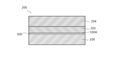
- the CIGS solar cell 1000 of the present embodiment includes a substrate 100, a back electrode 200 disposed on one surface 100 A of the substrate 100, and a photoelectric conversion layer 300.
- the photoelectric conversion layer 300 includes a chalcopyrite semiconductor layer 320 (hereinafter referred to as “semiconductor layer 320”), a buffer layer 330, a high resistance transparent electrode layer 342, and a low resistance transparent electrode layer 344.
- the layers of the photoelectric conversion layer 300 are formed in this order on the surface of the back electrode 200.
- the back electrode 200 includes a first metal layer 202 and a second metal layer 204.
- the first metal layer 202 is disposed on one surface 100A of the substrate 100, and a metal exhibiting higher conductivity and higher sputter rate than molybdenum (Mo) is formed on the film.
- the second metal layer 204 is formed of a film of Mo in contact with the first metal layer 202.
- Each of the first metal layer 202 and the second metal layer 204 is, for example, a film having an average film thickness of 100 nm or more.
- Sunlight h ⁇ for power generation is incident on the semiconductor layer 320 from the side of the buffer layer 330 located on the upper side of the drawing through the transparent electrode layer 340.
- FIG. 2 is a flowchart showing a method of manufacturing a CIGS solar cell 1000 including a step of forming a back surface electrode.
- the back electrode 200 is formed on the substrate 100.
- the first metal layer 202 which is a metal film exhibiting a higher conductivity and a higher sputtering rate than molybdenum (Mo)
- Mo molybdenum
- the semiconductor layer 320 is formed as the first layer of the photoelectric conversion layer 300 in contact with the back electrode 200 (step of forming a chalcopyrite semiconductor layer, S118).
- a selenization method or a co-evaporation method can be employed.
- an In / (Cu, Ga) laminated film to be a precursor is formed, and heating is performed in an atmosphere containing selenium (Se).
- a semiconductor layer having a target composition ratio is formed while separately controlling deposition sources of In, Cu, Ga, and Se.
- the buffer layer 330 in contact with the semiconductor layer 320 is formed (buffer layer forming step, S120).
- a Cd-based or Zn-based thin film for example, a CdS thin film is formed.
- the buffer layer 330 is formed by a CBD (Chemical Bath Deposition) method, a sputtering method, or an evaporation method.
- the high resistance transparent electrode layer 342 and the transparent electrode layer 344 are formed on the surface of the buffer layer 330 (high resistance transparent electrode layer forming step S122 and low resistance transparent electrode layer forming step S124).
- the high-resistance transparent electrode layer and the subsequent layers can be formed by sputtering or MOCVD.
- the photoelectric conversion layer 300 including the back electrode 200, the semiconductor layer 320, the buffer layer 330, the high-resistance transparent electrode layer 342, and the transparent electrode layer 344 is formed on the surface of one surface 100A.
- a grid electrode of metal such as Al may be formed on the surface of the transparent electrode layer 344 as necessary.
- FIG. 3 is a schematic cross-sectional view showing several configurations of the back electrode, the basic configuration (FIG. 3 (a)), the configuration to which the texture structure is added (FIG. 3 (b)), and the second metal layer It is a schematic sectional drawing shown as a structure (FIG.3 (c)) which coat
- the back electrode 200 includes a first metal layer 202, which is a metal film disposed on one surface 100A of the substrate 100, and a second metal layer 204, which is a Mo film in contact with the first metal layer 202. Is equipped.
- the material of the second metal layer 204 is Mo.
- the material of the first metal layer 202 is a metal that exhibits higher conductivity and higher sputter rate than molybdenum (Mo).
- the sputtering rate is the number of incident atoms of the target material per the number of atoms of the sputtering gas (Ar) incident on the target surface.
- the sputtering rate is Ar, and the sputtering rate is determined by the value in the state of ion energy 500 eV, for example, determined by the values listed in Table 8.1 (pages 200 to 201) of Non-Patent Document 1. be able to.
- Non-Patent Document 1 As the sputtering rate of Mo as a reference, although the values of 0.64 and 0.8 are described in Non-Patent Document 1, the value of 0.64 is adopted in the present application.
- Typical examples of metals selected as the first metal layer 202 under this criterion are Au, Ag, Cu, Pt, Pd, Ni and Al.
- Mo is 0.64 pieces
- Al is 1.05 pieces
- Ag is 2.3 to 3.12 pieces
- Cu is 1.0 to 2.35 pieces
- Pt is 1.40 pieces
- the Pd content is 2.08, and the Ni content is 1.33 or 1.45.
- These metals can be adopted as single metals or as alloys containing any of them, as long as the above criteria are satisfied.
- the conductivity can be compared as the electrical conductivity in the bulk state (reciprocal of the electrical resistivity), or in the actual thin film, as the sheet resistance at the same film thickness.
- the first function of the second metal layer 204 has a role of protecting the first metal layer 202 from Se during deposition of the semiconductor layer 320 (protection function).
- the protective function is useful when the semiconductor layer 320 contains Se or Se is present in the process of forming the semiconductor layer 320.
- the second metal layer 204 is too thin, the effect can not be expected.
- the thickness of the second metal layer 204 is made such that it can be made into a film.
- the second metal layer 204 is formed to have an average film thickness of 100 nm or more.
- the second function of the second metal layer 204 is a function that facilitates mechanical scribing (scribing function).
- the scribe function is obtained by the fact that the c-plane of MoSe 2 formed by the reaction with Se grows perpendicularly to the Mo surface, and the Van der Waals force weakly bonds between planes parallel to the c-plane. The reason is that patterning becomes easy.
- Mo () which is as hard as about 5.5 in Mohs hardness is useful for preventing damage to the back electrode at the time of scribing.
- the actual thicknesses of the first metal layer 202 and the second metal layer 204 are determined in accordance with the specific photoelectric conversion element design.
- the material of the first metal layer 202 is higher in conductivity and sputter rate than Mo of the second metal layer 204, so the thicker the first metal layer 202, the better from the electrical characteristics.
- the second metal layer 204 has a thickness that can sufficiently exhibit the protective function.
- membrane it is so preferable that it is thin from a viewpoint of productivity.
- the electrical requirement is determined, for example, by the value of the sheet resistance of the entire back electrode 200.
- the thickness of the second metal layer 204 is determined from the viewpoint of the protective function.
- the thickness of the first metal layer 202 is determined from the viewpoint of compensating the conductivity by which the thickness of the second metal layer 204 is insufficient due to the electrical requirements by the first metal layer 202.
- the reason why the first metal layer 202 is formed to a thickness of, for example, 100 nm or more is that a film having a certain thickness is required to be responsible for the electrical conduction.
- the back surface electrode 210 is advantageous in that the light trapping effect can be expected as a back surface electrode for a photoelectric conversion element if it has a texture structure, that is, a structure in which fine asperities are provided. Such irregularities should finally form irregularities on the surface of Mo of the second metal layer 204, and various methods may be adopted such that the surface becomes an uneven reflective surface exhibiting diffuse reflectivity to light. it can.
- One of the typical examples of the method is a method in which the surface is made an uneven reflection surface only in the second metal layer 204 without forming the unevenness in the substrate 100 or the first metal layer 202.
- Another typical example is a method of forming asperities on the base on which the second metal layer 204 is to be formed although the asperities are not particularly formed in the second metal layer 204.
- FIG. 3B as a configuration of an example of the first metal layer 212 and the second metal layer 214 in the case of forming the unevenness, the unevenness formed in the first metal layer 212 is reflected in the second metal layer 214. Shows the configuration.
- FIG. 4 is a configuration diagram illustrating the configuration of the imprint apparatus 600 in an example method for forming asperities on the surface of the second metal 214 in the present embodiment.
- An imprint method which is a technology for realizing microfabrication, is applied to the mold roller 630 by pressing the surface of the second metal layer 214 against the substrate.
- a laminated electrode in a state without particularly unevenness is formed on one surface 100 A of the substrate 100 in the layer to be the first metal layer 212 and the layer to be the second metal layer 214. Then, the surface (Mo surface) of the second metal layer 214 formed on the surface side of the laminated electrode is brought into contact with the surface of the mold roller 630. On the surface of the mold roller 630, a fine concavo-convex shape to be an original texture is formed in advance. Then, the substrate 100 is fed toward the mold roller 630 by the pressure roller 640 while pressing the surface of the substrate 100 on the second metal layer 214 side. The substrate 100 is, for example, in a long state, and sent from the unwinding roll 610 to the winding roll 620. Such a process can form a desired texture structure with high efficiency.
- asperities are formed on the interface between the first metal layer 212 and the second metal layer 214, that is, on the surface of the first metal layer 212
- a method of reflecting the unevenness to at least a certain extent to the surface of the second metal layer 214 will be described.
- the unevenness may be formed on the surface of the first metal layer 212 by any method.
- the second metal layer 214 is formed of Mo, for example, by sputtering, it is possible to form unevenness on the surface of the second metal layer 214 to the extent that light is diffused and reflected. As shown in FIG.
- the second metal layer 214 may be slightly flattened by the formation. However, if the unevenness is formed on the surface of the first metal layer 212 to be the base, the unevenness is reflected on the surface of the second metal layer 214 at least to some extent, so the unevenness of the surface of the second metal layer 214 is reflected It becomes a surface and contributes to the diffuse reflection of light.
- one preferable method of forming asperities on the surface of the first metal layer 212 which is a base for the second metal layer 214 is to control the substrate temperature to form the first metal layer 212.
- a texture due to asperities may be formed on the surface of the first metal layer 212 by forming the substrate 100 by sputtering while maintaining the substrate 100 at 100 ° C. or higher. It is possible.
- the substrate temperature is in the range of 100 ° C. to 250 ° C.
- the substrate temperature is a temperature adjusted from the viewpoint of adhesion (substrate / electrode) and surface morphology.
- corrugation in the surface of the 1st metal layer 212 is not limited to temperature control.
- the first metal layer 212 is formed on one surface 100A of the substrate 100 in advance so as to have irregularities formed in advance by the material of the substrate 100 or by a material different from the substrate 100.
- the unevenness can be further reflected to the outermost surface of the back electrode through the second metal layer 214.
- the first metal layer 222 is covered with the second metal layer 224 as shown in FIG.
- the back electrode 220 can also be employed.
- that the second metal layer 224 covers the first metal layer 222 means that the second metal layer 224 is in contact with all the surfaces of the first metal layer 222 on the opposite side to the substrate, and further the first metal This means that the second metal layer 224 extends to at least a part of one surface 100A of the substrate 100 where the layer 222 is not formed.
- the first metal layer 222 By covering the first metal layer 222 with the second metal layer 224 as described above, it is possible to prevent Se from chemically reacting with the second metal layer 214 in the chalcopyrite semiconductor layer forming step S118. That is, the first metal layer 222 is protected from Se by the second metal layer 224.
- the film formation area In order to make the film formation area smaller than that of the second metal layer 224 that follows the first metal layer 222, the film formation area is limited using a mask at the time of film formation, or after the film formation of the first metal layer 222. It is useful to perform processing such as removing the periphery by etching.
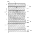
- FIG. 5 is a schematic cross-sectional view of a back electrode configured to employ a metal layer called Glue layer 500 that improves the adhesion between the substrate and the electrode layer.
- Glue layer 500 On one surface 100A of the substrate 100, for example, a metal layer such as Cr or Ti is formed, and then a first metal layer 202 is formed.
- the role of the glue layer 500 is to increase the adhesion of the first metal layer 202 to the one surface 100A.
- FIG. 6 is a schematic cross-sectional view showing the structure of the CIGS solar cell 1100 in the present embodiment.
- the difference between the CIGS solar cell 1100 and the CIGS solar cell 1000 shown in FIG. 1 is that the back electrode 400 is formed in the CIGS solar cell 1100.
- the layer of the back electrode 400 is formed at the time of forming the semiconductor layer 320 (chalcopyrite type semiconductor layer forming step S118, FIG. 2) It is the case.
- the outermost layer at this time is a metal other than Mo and the layer is formed on the other surface 100B
- the material of the layer is influenced by Se in the atmosphere in the chalcopyrite semiconductor layer forming step S118. You will receive So, in the CIGS solar cell 1100 of this embodiment, the influence is prevented by two approaches.
- the first approach is to form the fourth metal layer 414 made of Mo on the third metal layer 412 while making the third metal layer 412 a metal that exhibits higher conductivity and higher sputter rate than Mo. is there.
- the fourth metal layer 414 made of Mo is not used, and by the device of the film forming apparatus, the influence of Se in the atmosphere is prevented from being applied to the other surface 100B.
- the back electrode 400 may be provided for other purposes.
- the third metal layer 412 is protected from Se by the fourth metal layer 414, the third metal layer 412 can be adopted, and the high-performance back electrode 400 has a high production efficiency. It is possible to form in If this approach is adopted, it should be noted that the back electrode 400 does not necessarily need the third metal layer 412 depending on the specific design of the CIGS solar cell 1100, and may be only the fourth metal layer 414. is there. In such a case, the configuration of the back electrode 400 that can utilize the Se corrosion resistance of Mo is a chalcopyrite semiconductor layer on one side 100A of all or part of the metal layer of the back electrode 400. When 320 is formed, the material of the layer positioned on the outermost surface on the side of the other surface 100B is Mo.
- the advantage of balancing on both sides of the substrate 100 can also be expected in the fourth metal layer 414 of the back electrode 400. That is, in the case where the chalcopyrite-based photoelectric conversion does not contain selenium (Se), such as CIS, the action of Mo for avoiding the influence of Se is irrelevant. In addition, on the other surface 100 B side of the substrate 100, there is no request for ohmic contact. However, that does not mean that the necessity of using Mo for the back is completely eliminated. It is because manufacture of the CIGS solar cell 1100 becomes easy by setting it as the structure with a favorable balance on both surfaces of the board
- the second approach is to use a shield-like mask such that the distance between the mask covering the outside of the film forming area and the substrate is made smaller in the film forming apparatus, or the flexible substrate end is completely covered. It is effective to limit the Se irradiation range and reduce the backflow of Se. Thus, the Se gas is prevented from coming around the second surface 100B. Even if the chalcopyrite-based photoelectric conversion contains selenium (Se) by adopting the device on the film forming apparatus, the back electrode 400 does not necessarily require the fourth metal layer 414, and Only the metal layer 412 can be used.
- SCAF-CIGS solar cell 1200 an integrated chalcopyrite-type photoelectric conversion element 1200 (hereinafter, referred to as “SCAF-CIGS solar cell 1200”) will be described.
- the SCAF-CIGS solar cell 1200 applies a series connection structure utilizing the both sides of a substrate called an SCAF structure to a chalcopyrite photoelectric conversion element.
- FIG. 7 and 8 are a plan view and a schematic cross-sectional view showing the structure of the SCAF-CIGS solar cell 1200.
- FIG. FIG. 9 is a flowchart showing a process of manufacturing the SCAF-CIGS solar cell 1200.
- the SCAF-CIGS solar cell 1200 is described in relation to the CIGS solar cell 1100 (FIG. 6) in addition to the substrate 100, the back electrode 200, the photoelectric conversion layer 300 described in relation to the CIGS solar cell 1000 (FIG. 1)
- a connection wiring layer 420 similar to the back electrode 400 is provided.
- a film substrate is employed as the substrate 100.
- connection wiring layer 420 for establishing a series connection using the photoelectric conversion layer 300.
- the connection wiring layer 420 further has a fifth metal layer 426 and the substrate 100 laminated on the fourth metal layer 424.
- the photoelectric conversion layer 300 is a plurality of photoelectric conversion regions 300 1 and 300 2 which are separated from each other by a separation line SL 1 .
- the connection wiring layer 420 is also a plurality of connection wiring regions 420 1 and 420 2 which are separated from each other by the separation line SL 2 .
- connection wiring region (for example, the connection wiring region 420 2 ) is opposed to the two photoelectric conversion regions 300 1 and 300 2 adjacent to each other on the side of one surface 100 A of the substrate 100 with the substrate 100 interposed therebetween. It is arrange
- Another aspect of the back electrode 200 of the photoelectric conversion region 300 2 one extending to the inner wall of the first through hole 102 through the extension of the back electrode 200 extending on the inner wall of the first through hole 102 penetrating the substrate 100 It is connected to the connection wiring region 420 2.
- Another photoelectric conversion region 300 1 of the transparent electrode layer 340 extending to the inner wall of the second through hole 104 through the extension of the transparent electrode layer 340 extending to the inner wall of the second through hole 104 penetrating the substrate 100 It is connected to the one connection wiring area 3001.
- a series connection of the plurality of photoelectric conversion regions 300 1 and 300 2 is established by the plurality of connection wiring regions 420 1 and 420 2 .
- the solar cell 1200 functions as a substrate type integrated thin film solar cell in which serial connection is established, and becomes a flexible chalcopyrite solar cell formed on the substrate 100 which is an insulator film.
- the substrate 100 is first formed with an opening for the first through hole 102 (series connection hole). For this purpose, an opening is provided at a predetermined position of the substrate 100 by a punching die (punch) (first through hole forming step S102).
- the substrate 100 is heated under reduced pressure to perform degassing processing S104 for removing the gas released from the polyimide film of the material of the substrate 100.
- the degassing process S104 may be performed either before or after the first through hole forming process S102.
- the first metal layer 202 is formed on one surface 100A of the substrate 100 (first metal layer forming step S106), and the second metal layer 204 is further formed (second metal layer forming step S108).
- a layer to be the third metal layer 422 is formed on the other surface 100B of the substrate 100 (third metal layer forming step S110), and a layer to be the fourth metal layer 424 is further formed (fourth metal layer forming step S112).
- the first metal layer 202 is formed by sputtering, for example, Al to a film thickness of 300 nm.
- the second metal layer 204 is formed by sputtering Mo to a film thickness of 200 nm.
- the material of the third metal layer 422 is, for example, Al as in the layer to be the first metal layer 202, and as the material of the fourth metal layer 424, for example, the same Mo is used as the layer to be the second metal layer 204. Do. Note that as the material of the layer to be the first metal layer 202 and the material of the third metal layer 422, metals other than Al, such as metals having higher conductivity and higher sputtering rate than Mo and alloys thereof can be used.
- the third metal layer 422 and the layer of the fourth metal layer 424 formed in the above also extend to the inside of the first through hole 102 (series connection hole). Therefore, the metal layers on both sides of the substrate 100 directly overlap each other at or near the inner wall surface of the first through hole 102, and these layers are electrically connected to each other (FIG. 8).
- the first surface patterning step S114 is performed, and the third metal layer 422 formed on one surface 100A (first surface) of the substrate 100 at that time and The fourth metal layer 424 is separated at a separation line SL1.
- an opening for a second through hole 104 (current collecting hole) is formed in the substrate 100 using a punching die different from the case of the first through hole 102 (second through hole forming step S116).
- the second through hole 104 penetrates not only the substrate 100 but also the first metal layer 202, the second metal layer 204, the third metal layer 422, and the fourth metal layer formed on the substrate 100. It is 424.
- the first metal layer 202, the second metal layer 204, the third metal layer 422, and the fourth metal layer 424 are cut at the cross section of the second through hole 104, and the second through hole 104 is formed. There are no electrodes inside.
- the second through hole 104 (current collecting hole) is finally used for current collection, and the third metal layer 422, the fourth metal layer 424 or the fifth metal layer 426 (fifth).
- the transparent electrode layer 340 (formed in the low resistance transparent electrode layer forming step S124) is connected to the metal layer forming step S126). If a sufficient number of second through holes 104 are formed, it is difficult to increase the power loss of the entire substrate 100 even if the transparent electrode layer 340 is a transparent conductive material having a high sheet resistance.
- a photoelectric conversion layer 300 including a CIGS semiconductor layer and the like is formed on the side of one surface 100A of the substrate 100.
- the photoelectric conversion layer 300 first, the CIGS semiconductor layer 320 in contact with the back electrode 200 is formed in the CIGS layer forming step S118. Then, in the buffer layer formation step S120, the buffer layer 330 is formed on the CIGS semiconductor layer 320 on one side 100A.
- the film forming method at the time of forming the CIGS semiconductor layer 320 and the buffer layer 330 is not particularly limited.
- the buffer layer 330 is formed on one surface 100A, so the transparent electrode layer 340 is formed in the high resistance transparent electrode layer forming step S122 and the low resistance transparent electrode layer forming step S124.
- the high resistance transparent electrode layer 342 and the low resistance transparent electrode layer 344 are formed by sputtering using targets of respective materials.
- a mask is applied to the both end portions (FIG. 7) of the photoelectric conversion layer 300, that is, the portions where the first through holes 102 are provided, so that the transparent conductive material is not deposited.
- the photoelectric conversion layer 300 is exposed in this portion, and the transparent electrode layer 340 is not formed in the region of the first through hole 102.
- the fifth metal layer 426 is formed on the surface of the fourth metal layer 424.
- RF sputtering, DC sputtering, a printing method, a coating method, etc. are also employable as a film-forming method of high resistance transparent electrode layer formation process S122 and low resistance transparent electrode layer formation process S124.
- a layer of a fifth metal layer 426 forming the connection wiring layer 420 together with the third metal layer 422 and the fourth metal layer 424 is formed on the entire surface on the other surface 100B side of the substrate 100 (a fifth metal layer forming step S126).
- a low resistance conductive layer such as a metal material such as nickel is formed.
- the layer to be the transparent electrode layer 340 formed on one surface 100A of the substrate 100 and the layer to be the fifth metal layer 426 formed on the other surface 100B of the substrate 100 are They are overlapped directly on or near the inner wall surface of the second through hole 104 and are electrically connected to each other (FIG. 8).
- the fifth metal layer 426 is formed to be in contact with the fourth metal layer 424 on the other surface 100 B of the substrate 100. Therefore, the third metal layer 422, the fourth metal layer 424, and the fifth metal layer 426 on the other surface 100B are electrically connected to each other to form a laminated film for the connection wiring layer 420.
- the CIGS semiconductor layer 320 and the buffer layer 330 have the same shape as the back electrode 400.
- the transparent electrode layer 340 is not formed in the vicinity of the first through hole 102, but the vicinity of the separation line SL1 is divided at the same position as the back electrode 200.
- a unit cell is formed in which the back electrode 200, the CIGS semiconductor layer 320, the buffer layer 330, and the transparent electrode layer 340 are stacked in this order except for the vicinity of the end in the shape surrounded by the separation line SL1.
- the first surface patterning step S128 shown here it is preferable to perform a preliminary patterning process (for example, the first surface patterning step S114) in order to more reliably perform the step of forming a unit cell.
- This preliminary patterning process is performed, for example, at any stage after the second metal layer forming step S108 and before the CIGS layer forming step S118. Also in this preliminary patterning process, it is the position of the separation line SL1 that the back electrode 200 is patterned so as to separate.
- the SCAF-CIGS solar cell 1200 can be manufactured. Then, in order to ensure durability, it seals with a sealing material and a protection sheet (all are not illustrated).
- the SLG substrate used as pretreatment of the substrate was washed with pure water and IPA (isopropyl alcohol).
- a back electrode was formed.
- Al is adopted as the first metal layer 202 from among metals (Au, Ag, Cu, Pt, Pd, Ni, Al and alloys containing these elements) having high sputtering rate and conductivity.
- the DC magnetron sputtering method was adopted as a means of film formation.
- the substrate temperature was 50.degree.
- the first metal layer 202 was not formed.
- the second metal layer 204 was formed on the first metal layer 202 so as to completely cover the first metal layer. Sputtering was mainly used as a method of forming the electrode.
- FIG. 10 shows sheet resistances of Mo and Al single films for each film thickness formed under the same conditions as the example, that is, DC magnetron sputtering, input power 300 W, target / substrate distance 10 cm.
- the inventor of the present application has determined that the sheet resistance for a photoelectric conversion element after commercialization is 0.5 ⁇ / ⁇ or less.
- the film thickness 500 nm or more it is necessary to make the film thickness 500 nm or more based on the actual measurement value of FIG.
- the film forming rate is 33.3 nm / min, and the film forming time requires 15 minutes.
- the thickness of Mo used as the second electrode layer 204 is set to 200 nm which is thin as long as the protective function can sufficiently perform.
- the thickness of the first metal layer 202 was determined to be 300 nm from the viewpoint of compensating the conductivity by the first metal layer 202 because the second electrode layer 204 alone does not reach the reference sheet resistance of 0.5 ⁇ / ⁇ . .
- the film forming time could be reduced by about 30% from 15 minutes to about 10 minutes while satisfying the sheet resistance requirements.
- the sputtering apparatus for the first metal layer 202 and the second metal layer 204 uses the same DC magnetron sputtering as that used in the comparative example, and the input power 300 W and the distance between the target and the substrate are 10 cm. did.
- the film formation time required for forming the Al layer of the first metal layer 202 is 3.75 minutes at a film formation rate of 80 nm / min.
- the Mo layer of the second metal layer 204 under the same conditions has a film formation rate of 33. It was 3 nm / min, and the film formation required time was 6 minutes.
- the substantial sheet resistance by this combination was 0.45 ohms / square.
- the structure of the back surface electrode 200 is made into the basic composition shown to Fig.3 (a), and the unevenness
- a CIGS semiconductor layer was formed as a semiconductor layer 320 by a selenization method.
- a selenization method first, an In / (Cu, Ga) laminated film was formed as a precursor on the surface of the second electrode layer 204 by a sputtering method. Then, the precursor was annealed at 550 ° C. in H 2 Se gas to form CIGS as a semiconductor layer 320.
- a thin film of CdS was formed as the buffer layer 330, and the high resistance transparent electrode layer 342 and the transparent electrode layer 344 were formed thereon.
- the high-resistance transparent electrode layer 342 and the transparent electrode layer 344 were formed by sputtering to form a ZnO layer and a ZnO: Al layer (aluminum-doped ZnO layer). Finally, an Al grid electrode was formed by vapor deposition.
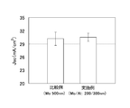
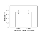
- FIGS. 11 to 14 show the characteristic evaluation results of the comparative example and the example.
- the number of samples was set at 12 pieces, and the characteristics were represented by the bar height of the average value between samples and the error bar showing the range from the minimum value to the maximum value due to the sample-to-sample variation in each condition.
- Vcc open circuit voltage
- Jsc short circuit current density
- FF fill factor
- the configuration showing the characteristics of the photoelectric conversion element in the above embodiment is only the one in which the CIGS semiconductor layer is adopted as the chalcopyrite type semiconductor layer.
- the method of the present embodiment can be similarly applied to a photoelectric conversion element employing another chalcopyrite semiconductor material.
- the back electrode 200 (FIG. 1) formed before the formation of the semiconductor layer 320 has a function of protecting the second metal layer 204 from Se of the first metal layer 202, a scribing function, and a fourth function.
- the type of the semiconductor layer 320 does not greatly affect the function of exerting at least one of the functions of achieving the function of balancing the both sides of the substrate in the metal layer 414 (FIG. 6) and the fourth metal layer 424 (FIG. 8). It is for.
- the second metal layer 204 has a protective function even when the vapor deposition method is employed instead of the selenization method. Demonstrate. Further, the second metal layer 204 can also be expected to have an effect of reducing or avoiding the influence of Se in the semiconductor layer 320 on the first metal layer 202 in the use stage after manufacture, not in the film formation stage.
- the photoelectric conversion element and back surface electrode of the present invention can be used for any device that generates electric power by light such as sunlight.
- chalcopyrite type photoelectric conversion element CIGS solar cell
- SCAF-CIGS solar cell 100 substrate 100A one surface 100B other surface 102 first through hole 104 second through hole 200, 210, 220 back surface electrode 202, 212, 222 first metal layer 204, 214, 224 second metal layer 300 photoelectric conversion layer 320 Chalcopyrite semiconductor layer 330 buffer layer 340 transparent electrode layer 342 high resistance transparent electrode layer 344 transparent electrode layer 400 back surface electrode 420 connection wiring layer 412, 422 third metal layer 414, 424 fourth metal layer 426 fifth metal layer SL1, SL2 separation line
Abstract
カルコパイライト系光電変換素子に適する裏面電極を効率良く製造する。本発明のある実施形態の裏面電極200は、第1金属層202と第2金属層204とを備えている。第1金属層202は、基板100の一方の面100Aの上に配置され、モリブデン(Mo)より高い導電率および高いスパッタ率を示す金属により形成されている。第2金属層204は、第1金属層202に接しているMoの膜である。本発明の実施形態では、さらに光電変換層300を備えるカルコパイライト系光電変換素子1000も提供される。光電変換層300は、カルコパイライト型半導体層320と、バッファー層330と、高抵抗透明電極層342と、低抵抗の透明電極層344とを含み、各層が裏面電極200の面の上にこの順に形成されている。
Description
本発明は、カルコパイライト型光電変換素子、裏面電極、およびその製造方法に関する。さらに詳細には本発明は、製造効率を高めたカルコパイライト型光電変換素子、裏面電極、およびその製造方法に関する。
近年、カルコパイライト(chalcopyrite)型光電変換素子がその高い光電変換効率により注目を集めている。カルコパイライト型光電変換素子は、I-III-VI族元素を利用した化合物半導体を光電変換層に含むものであり、代表的な半導体の組成は、CIS(CuInS2)、CIGS(Cu(In,Ga)Se2)、CIGSS(Cu(In,Ga)(Se,S)2)とも呼ばれる組成である。カルコパイライト型光電変換素子では、オーミック接合の形成、Seに対する腐食耐性、加工性向上等の観点から、光電変換層の光が入射する側とは逆の電極(裏面電極)としてMoの単膜が使用されている。また、カルコパイライト型光電変換素子では、Naにより特性が向上することが知られており、SLG(ソーダライムガラス)基板を使用するカルコパイライト型光電変換素子では、SLG基板からMoの裏面電極を通してNaを供給することも行なわれる。
一方、薄膜系太陽電池の構造として、基板などの両面を繋ぐ貫通孔を有する太陽電池が提案されている(例えば特許文献1)。さらに、SCAF構造(Series Connection through Apertures Formed on Film、特許文献1、図1)に代表される、フィルム基板に空けた貫通孔を通じ各ユニットセルの直列接続を形成する手法も実用化されている。
麻薪立男、「薄膜作成の基礎」第3版、日刊工業新聞社、1996年
カルコパイライト型光電変換素子にて採用される裏面電極の材料としてのMoには、高性能な光電変換素子の生産の障害となりかねない以下の課題がある。第1に、Moは抵抗率が高く太陽電池モジュールの直列抵抗成分が増大してしまう。例えばAl(アルミニウム)およびAg(銀)の電気抵抗率がそれぞれ2.8×10⁻⁸Ω・mおよび1.5×10⁻⁸Ω・mであるのに対し、Moは5.3×10⁻⁸Ω・mである。第2に、Moはスパッタ率が低く成膜速度が遅い。例えば1個のスパッタガス原子の入射によりスパッタリングされて飛散する原子の数は、AlおよびAgが1.05および2.3~3.12個程度であるのに対し、Moは0.64または0.80である(例えば、非特許文献1、第198~201頁)。しかも、上記課題の組合せは、裏面電極による抵抗ロスを低減するためにMoを厚く成膜するという解決策を採用しがたいことも意味している。
本発明は上記問題点の少なくともいずれかを解決するためになされたものである。本発明は、カルコパイライト系光電変換素子に用いるために十分な性能の裏面電極を高い効率で生産することを可能にすることにより、高性能で生産性の高い光電変換素子の実現に貢献するものである。
上記課題を吟味した結果、本願の発明者は、CIS系などのカルコパイライト型光電変換素子において、CIS系半導体層に接する位置にMoの電極を配置しつつ、Moの上記課題を回避する手法を創出した。本発明においては、Moの膜とともに、Moとは異なる種類の金属膜を利用する。
すなわち本発明のある態様においては、基板と、該基板の一方の面の上に配置された裏面電極とを備えており、カルコパイライト型半導体層と、バッファー層と、高抵抗透明電極層と、透明電極層とを含む光電変換層が前記裏面電極の面の上にこの順にさらに形成されており、該裏面電極は、前記基板の前記一方の面の上に配置され、モリブデン(Mo)より高い導電率および高いスパッタ率を示す金属の膜である第1金属層と、該第1金属層に接しており、Moの膜である第2金属層とを有しており、前記基板の他方の面の上に金属層を備えており、前記他方の面の上の前記金属層の全体またはその一部の層のうち、前記一方の面の上にカルコパイライト型半導体層が形成される際に前記他方の面の側にて最表面に位置する層の材質がMoであるカルコパイライト型光電変換素子が提供される。
また、本発明のある態様においては、基板と、該基板の一方の面の上に配置された裏面電極とを備えており、カルコパイライト型半導体層と、バッファー層と、高抵抗透明電極層と、透明電極層とを含む光電変換層が前記裏面電極の面の上にこの順にさらに形成されており、該裏面電極は、前記基板の前記一方の面の上に配置され、モリブデン(Mo)より高い導電率および高いスパッタ率を示す金属の膜である第1金属層と、該第1金属層に接しており、Moの膜である第2金属層とを有しており、前記基板がフィルム基板であり、前記基板の他方の面の上に、第3金属層、第4金属層、および第5金属層が該基板からこの順に積層されている接続配線層をさらに備えており、前記光電変換層が互いに区切られた複数の光電変換領域となっており、前記接続配線層が互いに区切られた複数の接続配線領域となっており、各接続配線領域は、前記基板の前記一方の面の側において互いに隣接する二つの光電変換領域に前記基板を挟んで対向するようにして前記他方の面の側に配置されており、一の光電変換領域の裏面電極が、前記基板を貫通する第1貫通孔の内壁に延びた当該裏面電極の延長部を通じて該第1貫通孔の内壁に延びた一の接続配線領域に接続しており、別の光電変換領域の透明電極層が、前記基板を貫通する第2貫通孔の内壁に延びた当該透明電極層の延長部を通じて該第2貫通孔の内壁に延びた前記一の接続配線領域に接続しており、これにより、前記複数の光電変換領域の直列接続が前記複数の接続配線領域により確立されているカルコパイライト型光電変換素子も提供される。
さらに本発明は、カルコパイライト型光電変換素子のための裏面電極の態様によっても実施される。すなわち、本発明においては、基板の一方の面の上に配置され、モリブデン(Mo)より高い導電率および高いスパッタ率を示す金属の膜である第1金属層と、該第1金属層に接しており、Moの膜である第2金属層とを備えてなり、前記第2金属層の表面が凹凸を有し光に対し拡散反射性を示す凹凸反射面となっており、前記第1金属層と前記第2金属層との間の界面が凹凸を有しており、該第2金属層の前記凹凸反射面が該界面の界面が凹凸を反映したものであるカルコパイライト型光電変換素子のための裏面電極も提供される。
さらに、本発明においては、裏面電極の製造方法も提供される。
ここで、本発明の各態様において採用するカルコパイライト型半導体材料は、CIGS(Cu(In,Ga)Se2)以外にも、CIS(CuInS2)やCIGSS(Cu(In,Ga)(Se,S)等のI-III-VI族元素を利用した化合物半導体とすることができる。
また、何らかの面の上に形成されている(formed on or over a surface)状態やその処理は、面に接して形成される状態や処理と、他の何らかの層を介して、当該面の側に形成される状態や処理との双方を含んでいる。
本発明のいずれかの態様においては、電気抵抗を低下させつつ成膜処理速度を高めた裏面電極およびそれを利用するカルコパイライト系光電変換素子を製造することが可能となる。
以下、本発明に係る光電変換素子の実施形態を、裏面電極の実施形態とともに図面を参照して説明する。当該説明に際し特に言及がない限り、全図にわたり共通する部分または要素には共通する参照符号が付されている。また、図中、各実施形態の要素のそれぞれは、必ずしも互いの縮尺比を保って示してはいない。
[1 実施形態]
本実施形態においては、カルコパイライト系光電変換素子、裏面電極、およびその製造方法の実施形態を説明する。また、本実施形態では、カルコパイライト型光電変換素子を代表させCIGS太陽電池を説明する。
本実施形態においては、カルコパイライト系光電変換素子、裏面電極、およびその製造方法の実施形態を説明する。また、本実施形態では、カルコパイライト型光電変換素子を代表させCIGS太陽電池を説明する。
[1-1 光電変換素子の概略構成]
図1は、本実施形態のCIGS太陽電池1000の構造を示す概略断面図である。
図1は、本実施形態のCIGS太陽電池1000の構造を示す概略断面図である。
本実施形態のCIGS太陽電池1000は、基板100と、基板100の一方の面100Aの上に配置された裏面電極200と光電変換層300とを備えている。光電変換層300は、カルコパイライト型半導体層320(以下、「半導体層320」と記す)と、バッファー層330と、高抵抗透明電極層342と、低抵抗の透明電極層344とを含んでおり、光電変換層300のこれらの層は裏面電極200の面の上にこの順に形成されている。
裏面電極200は、第1金属層202と第2金属層204とを備えている。第1金属層202は、基板100の一方の面100Aの上に配置され、モリブデン(Mo)より高い導電率および高いスパッタ率を示す金属が膜に形成されている。これに対し第2金属層204は、第1金属層202に接するMoの膜により形成されている。第1金属層202および第2金属層204は、それぞれ、例えば平均膜厚が100nm以上の膜である。半導体層320には、透明電極層340を通して紙面上の上方に位置するバッファー層330の側から、発電のための太陽光hνが入射する。
次に、図2を参照し、本実施形態のCIGS太陽電池1000の製造方法について説明する。図2は、裏面電極を形成する工程を含むCIGS太陽電池1000の製造方法を示すフローチャートである。まず基板100には裏面電極200が形成される。具体的には、基板100の一方の面100Aの上に、モリブデン(Mo)より高い導電率および高いスパッタ率を示す金属の膜である第1金属層202を形成する(第1金属層形成工程、S106)。そして、第1金属層202に接してMoの膜である第2金属層を形成する(第2金属層形成工程、S108)。
その後、裏面電極200に接する光電変換層300の最初の層として半導体層320を形成する(カルコパイライト型半導体層形成工程、S118)。半導体層320として例えばCIGS層を形成する場合、セレン化法や同時蒸着法(または多源蒸着法)を採用することができる。セレン化法では、プリカーサとなるIn/(Cu,Ga)積層膜を形成し、セレン(Se)を含む雰囲気中で加熱する。蒸着法では、In、Cu、Ga、Seの蒸着源を別々に制御しながら目的の組成比の半導体層を形成する。半導体層320を形成した後、半導体層320に接するバッファー層330を形成する(バッファー層形成工程、S120)。バッファー層330としては、Cd系またはZn系の薄膜、例えばCdS薄膜を形成する。また、バッファー層330はCBD(Chemical Bath Deposition)法やスパッタリング法、蒸着法により形成する。最後にバッファー層330の面の上に高抵抗透明電極層342および透明電極層344を形成する(高抵抗透明電極層形成工程S122および低抵抗透明電極層形成工程S124)。高抵抗透明電極層以降はスパッタリング法やMOCVD法で形成することができる。こうして、裏面電極200、半導体層320、バッファー層330、高抵抗透明電極層342および透明電極層344を有する光電変換層300を一方の面100Aの面の上に形成する。なお、透明電極層344の表面には、必要に応じてAl等の金属によるグリッド電極を形成する場合もある。
[1-2 裏面電極の詳細]
裏面電極200の詳細についてさらに説明する。図3は、裏面電極のいくつかの構成を示す概略断面図であり、基本構成(図3(a))、テクスチャ構造を付与した構成(図3(b))、そして第2金属層により第1金属層を被覆する構成(図3(c))として示す概略断面図である。裏面電極200は、基板100の一方の面100Aの上に配置された金属の膜である第1金属層202と、第1金属層202に接しているMoの膜である第2金属層204とを備えている。
裏面電極200の詳細についてさらに説明する。図3は、裏面電極のいくつかの構成を示す概略断面図であり、基本構成(図3(a))、テクスチャ構造を付与した構成(図3(b))、そして第2金属層により第1金属層を被覆する構成(図3(c))として示す概略断面図である。裏面電極200は、基板100の一方の面100Aの上に配置された金属の膜である第1金属層202と、第1金属層202に接しているMoの膜である第2金属層204とを備えている。
[1-2-1 裏面電極の材質]
第2金属層204の材質はMoである。これに対し、第1金属層202の材質は、モリブデン(Mo)より高い導電率および高いスパッタ率を示す金属である。ここで、スパッタ率は、また、スパッタ率は、スパッタリングガス(Ar)のターゲット表面への入射原子数あたりのターゲット材料の入射原子数である。本出願においては、スパッタリングガスをAr、イオンエネルギー500eVの状態における値によりスパッタ率を決定し、例えば非特許文献1の表8.1(第200~201頁)に掲載されている値により決定することができる。また、基準とするMoのスパッタ率は、0.64と0.8との値が非特許文献1には記載されているが、本出願では0.64の値を採用する。この基準の下で第1金属層202として選択される金属の典型例は、Au、Ag、Cu、Pt、Pd、Ni、およびAlである。ちなみに、Moが0.64個であるのに対し、Alは1.05個、Agが2.3~3.12個、Cuが1.0~2.35個、Ptが1.40個、Pdが2.08個、そしてNiが1.33または1.45個である。これらの金属は単体としても、また、いずれかを含む合金としても、上記基準を満たす限り採用することもできる。なお、導電率は、端的にはバルク状態での電気伝導率(電気抵抗率の逆数)として、または、実際の薄膜においては、同一膜厚でのシート抵抗として比較することができる。
第2金属層204の材質はMoである。これに対し、第1金属層202の材質は、モリブデン(Mo)より高い導電率および高いスパッタ率を示す金属である。ここで、スパッタ率は、また、スパッタ率は、スパッタリングガス(Ar)のターゲット表面への入射原子数あたりのターゲット材料の入射原子数である。本出願においては、スパッタリングガスをAr、イオンエネルギー500eVの状態における値によりスパッタ率を決定し、例えば非特許文献1の表8.1(第200~201頁)に掲載されている値により決定することができる。また、基準とするMoのスパッタ率は、0.64と0.8との値が非特許文献1には記載されているが、本出願では0.64の値を採用する。この基準の下で第1金属層202として選択される金属の典型例は、Au、Ag、Cu、Pt、Pd、Ni、およびAlである。ちなみに、Moが0.64個であるのに対し、Alは1.05個、Agが2.3~3.12個、Cuが1.0~2.35個、Ptが1.40個、Pdが2.08個、そしてNiが1.33または1.45個である。これらの金属は単体としても、また、いずれかを含む合金としても、上記基準を満たす限り採用することもできる。なお、導電率は、端的にはバルク状態での電気伝導率(電気抵抗率の逆数)として、または、実際の薄膜においては、同一膜厚でのシート抵抗として比較することができる。
[1-2-1-1 Moである第2金属層204の機能]
第2金属層204の第1の機能は、第1金属層202を半導体層320の成膜中のSeから保護する役割がある(保護機能)。保護機能が役に立つのは、半導体層320にSeが含まれるか、または、半導体層320の形成工程においてSeが存在する場合である。ただし、第2金属層204があまりに薄いとその効果は期待できない。このため第2金属層204の厚みは、膜に作製できる厚みに作製される。例えば、第2金属層204は平均膜厚が100nm以上に形成される。
第2金属層204の第1の機能は、第1金属層202を半導体層320の成膜中のSeから保護する役割がある(保護機能)。保護機能が役に立つのは、半導体層320にSeが含まれるか、または、半導体層320の形成工程においてSeが存在する場合である。ただし、第2金属層204があまりに薄いとその効果は期待できない。このため第2金属層204の厚みは、膜に作製できる厚みに作製される。例えば、第2金属層204は平均膜厚が100nm以上に形成される。
また、第2金属層204の第2の機能は、メカニカルスクライビングが容易となる機能である(スクライブ機能)。スクライブ機能得られるのは、Seとの反応で生成したMoSe2のc面がMo表面に垂直に成長しており、c面に平行な面間はファン・デル・ワールス力で弱く結合していることに起因しパターニングが簡単になるためである。一方、半導体層320がSeを含まないCIS半導体である場合であっても、モース硬度で5.5程度と硬いMo()はスクライブ時の裏面電極の損傷を防止するため有用である。
[1-2-1-2 厚みの決定法]
第1金属層202と第2金属層204の実際の厚みは、具体的な光電変換素子の設計に適合させて決定される。典型的には、第1金属層202の材質が、第2金属層204のMoより導電率もスパッタ率も高いため、電気的特性からは第1金属層202は厚いほど好ましい。これに対し、第2金属層204は、上記保護機能が十分に発揮できる程度の厚みとする。また、いずれの膜も、生産性の観点からは薄いほど好ましい。そこでこれらを満たす厚みの決定法としては、まず、CIGS太陽電池1000の具体的構成基づいて、電気的要件を、例えば裏面電極200全体のシート抵抗の値を以て決定する。次に第2金属層204の厚みを、保護機能の観点から決定する。そして、第2金属層204のその厚みで電気的要件のために不十分となる導電性を第1金属層202により補う観点から、第1金属層202の厚みを決定する。なお、第1金属層202が例えば100nm以上の厚みに作製される理由はこの電気伝導を担うためにある程度の厚みの膜であることが要請されるためである。
第1金属層202と第2金属層204の実際の厚みは、具体的な光電変換素子の設計に適合させて決定される。典型的には、第1金属層202の材質が、第2金属層204のMoより導電率もスパッタ率も高いため、電気的特性からは第1金属層202は厚いほど好ましい。これに対し、第2金属層204は、上記保護機能が十分に発揮できる程度の厚みとする。また、いずれの膜も、生産性の観点からは薄いほど好ましい。そこでこれらを満たす厚みの決定法としては、まず、CIGS太陽電池1000の具体的構成基づいて、電気的要件を、例えば裏面電極200全体のシート抵抗の値を以て決定する。次に第2金属層204の厚みを、保護機能の観点から決定する。そして、第2金属層204のその厚みで電気的要件のために不十分となる導電性を第1金属層202により補う観点から、第1金属層202の厚みを決定する。なお、第1金属層202が例えば100nm以上の厚みに作製される理由はこの電気伝導を担うためにある程度の厚みの膜であることが要請されるためである。
[1-2-2 裏面電極による拡散反射]
裏面電極210は、テクスチャ構造すなわち微細な凹凸を付与する構造とすると、光電変換素子のための裏面電極として光閉じ込め効果が期待できる点において有利である。このような凹凸は、最終的に第2金属層204のMoの表面に凹凸を形成し、その表面が光に対し拡散反射性を示す凹凸反射面となるような各種の手法を採用することができる。その手法の典型例の一つが、基板100や第1金属層202には凹凸を形成せず、第2金属層204のみにおいて表面を凹凸反射面とする手法である。また別の典型例が、第2金属層204においては特段凹凸を形成しないものの、第2金属層204を形成する下地に凹凸を形成する手法である。図3(b)には、凹凸を形成する場合の第1金属層212と第2金属層214の一例の構成として、第1金属層212に形成された凹凸が第2金属層214に反映されている構成を示している。
裏面電極210は、テクスチャ構造すなわち微細な凹凸を付与する構造とすると、光電変換素子のための裏面電極として光閉じ込め効果が期待できる点において有利である。このような凹凸は、最終的に第2金属層204のMoの表面に凹凸を形成し、その表面が光に対し拡散反射性を示す凹凸反射面となるような各種の手法を採用することができる。その手法の典型例の一つが、基板100や第1金属層202には凹凸を形成せず、第2金属層204のみにおいて表面を凹凸反射面とする手法である。また別の典型例が、第2金属層204においては特段凹凸を形成しないものの、第2金属層204を形成する下地に凹凸を形成する手法である。図3(b)には、凹凸を形成する場合の第1金属層212と第2金属層214の一例の構成として、第1金属層212に形成された凹凸が第2金属層214に反映されている構成を示している。
また、これらとは異なる典型例として、第1金属層212と第2金属層214を成膜した後に、第2金属層214の表面に型押しによりテクスチャを形成させることも有用である。その具体的手法を図4に基づいて説明する。図4は、本実施形態において第2金属214の表面に凹凸を形成するための一例の手法におけるインプリント装置600の構成を説明する構成図である。型ローラ630に対して、第2金属層214の表面を向けて基板に押し当てることで微細加工を実現する技術であるインプリント法を適用する。具体的には、まず、第1金属層212となる層および第2金属層214となる層の、特に凹凸のない状態での積層電極を、基板100の一方の面100Aに形成しておく。そしてその積層電極の表面側に成膜された第2金属層214の表面(Mo表面)を、型ローラ630の表面に接触させる。型ローラ630の当該表面には、原版テクスチャとなる微細な凹凸形状が予め形成されている。そして、加圧ローラ640により型ローラ630に向けて基板100の第2金属層214側の面を加圧しながら基板100を送る。基板100は、例えば長尺の状態にしておき、巻出しロール610から巻き取りロール620へと送る。このような工程により、所望のテクスチャ構造を高い効率で形成することができる。
次に、図3(b)に示したもう一つの典型例である、第1金属層212と第2金属層214との間の界面、つまり第1金属層212の表面に凹凸を形成し、第2金属層214の表面にまでその凹凸を少なくともある程度反映させる手法について説明する。第2金属層214の表面には凹凸を反映させるためには、任意の手法により、第1金属層212の表面に凹凸を形成しさえすればよい。例えば、第2金属層214をMoにより例えばスパッタリングにより形成すれば、光に拡散反射させる程度の凹凸を第2金属層214表面に形成することができる。図3(b)に示したように、第2金属層214を形成することによりわずかに平坦化される場合がある。ただし、下地となる第1金属層212の表面に凹凸を形成すれば、その凹凸は第2金属層214の表面に少なくともある程度の凹凸として反映されるため、第2金属層214の表面が凹凸反射面となって光の拡散反射に寄与することとなる。
そして、第2金属層214にとって下地となる第1金属層212の表面に凹凸を形成する一つの好適な手法が、基板温度を制御して第1金属層212を形成するものである。具体的には、第1金属層212としてAlを採用する場合、基板100を100℃以上に保ってスパッタリングにより形成することにより、第1金属層212の表面には凹凸によるテクスチャを形成することが可能である。例えば基板温度は100℃~250℃の範囲において基板温度については付着力(基板/電極間)と表面モフォロジーの観点から調整した温度とされる。
なお、第1金属層212の表面に凹凸を形成する手法は温度制御には限定されない。例えば基板100の一方の面100Aに、基板100の材質によりまたは基板100とは別の材質により予め凹凸を形成しておいて、それを少なくともある程度表面に反映させるように第1金属層212を形成すれば、さらに第2金属層214を通じてその凹凸を裏面電極の最表面にまで反映させることができる。
[1-2-3 Moによる第1金属層の保護の強化]
本実施形態のCIGS太陽電池1000においては、第2金属層による第1金属層の保護を強化するため、図3(c)に示すように第2金属層224により第1金属層222を覆う構成の裏面電極220を採用することもできる。ここで、第2金属層224が第1金属層222を覆うとは、第2金属層224が第1金属層222の基板とは反対側の面のすべてに接しているとともに、さらに第1金属層222が形成されていない基板100の一方の面100Aの少なくとも一部まで第2金属層224が広がっていることをいう。このように第2金属層224により第1金属層222を覆うことにより、カルコパイライト型半導体層形成工程S118においてSeが第2金属層214と化学反応することを防止できる。つまり、第2金属層224によりSeから第1金属層222が保護される。第1金属層222を続く第2金属層224よりも成膜面積を小さくするためには、成膜時にマスクを使用して成膜面積を制限すること、または成膜後に第1金属層222の周辺部をエッチングで除去するといった加工を行うことが有用である。
本実施形態のCIGS太陽電池1000においては、第2金属層による第1金属層の保護を強化するため、図3(c)に示すように第2金属層224により第1金属層222を覆う構成の裏面電極220を採用することもできる。ここで、第2金属層224が第1金属層222を覆うとは、第2金属層224が第1金属層222の基板とは反対側の面のすべてに接しているとともに、さらに第1金属層222が形成されていない基板100の一方の面100Aの少なくとも一部まで第2金属層224が広がっていることをいう。このように第2金属層224により第1金属層222を覆うことにより、カルコパイライト型半導体層形成工程S118においてSeが第2金属層214と化学反応することを防止できる。つまり、第2金属層224によりSeから第1金属層222が保護される。第1金属層222を続く第2金属層224よりも成膜面積を小さくするためには、成膜時にマスクを使用して成膜面積を制限すること、または成膜後に第1金属層222の周辺部をエッチングで除去するといった加工を行うことが有用である。
[1-2-4 Glue層]
本実施形態のCIGS太陽電池1000にはさらに種々の工夫を施すことが可能である。図5はGlue層500と呼ぶ基板と電極層の間の接着性を向上する金属層を採用する構成の裏面電極の概略断面図である。基板100の一方の面100Aには、例えばCr、Tiなどの金属層を形成し、その後に、第1金属層202を形成する。Glue層500の役割は、一方の面100Aに対して第1金属層202の付着力を高める作用である。
本実施形態のCIGS太陽電池1000にはさらに種々の工夫を施すことが可能である。図5はGlue層500と呼ぶ基板と電極層の間の接着性を向上する金属層を採用する構成の裏面電極の概略断面図である。基板100の一方の面100Aには、例えばCr、Tiなどの金属層を形成し、その後に、第1金属層202を形成する。Glue層500の役割は、一方の面100Aに対して第1金属層202の付着力を高める作用である。
[1-3 基板の両面を利用する光電変換素子]
次に、本実施形態のCIGS太陽電池1000の変形として、基板100の他方の面100Bに金属電極を形成するCIGS太陽電池1100の構成について説明する。図6は、本実施形態におけるCIGS太陽電池1100の構造を示す概略断面図である。CIGS太陽電池1100と図1に示したCIGS太陽電池1000との相違点は、CIGS太陽電池1100では背面電極400が形成されていることである。このCIGS太陽電池1100を作製するために問題となるのは、半導体層320を形成する時点(カルコパイライト型半導体層形成工程S118、図2)において背面電極400の少なくとも一部の層が形成されている場合である。この時点の最表面なっている層がMo以外の金属でありその層が他方の面100Bに形成されている場合、その層の材質がカルコパイライト型半導体層形成工程S118における雰囲気中のSeによる影響を受けることとなる。そこで、本実施形態のCIGS太陽電池1100においては、二つのアプローチによりその影響を防止する。第1のアプローチは、第3金属層412をMoより高い導電率および高いスパッタ率を示す金属としつつ、Moを材質とする第4金属層414を第3金属層412に重ねて形成するものである。これに対し、第2のアプローチにおいては、Moを材質とする第4金属層414を用いず、成膜装置の工夫によって、雰囲気中のSeによる影響が他方の面100Bに及ばないようにする。なお、CIGS太陽電池1100において背面電極400を設ける理由は、典型的には、後述する直列接続などのためであるが、背面電極400は他の目的で設けられるものとすることもできる。
次に、本実施形態のCIGS太陽電池1000の変形として、基板100の他方の面100Bに金属電極を形成するCIGS太陽電池1100の構成について説明する。図6は、本実施形態におけるCIGS太陽電池1100の構造を示す概略断面図である。CIGS太陽電池1100と図1に示したCIGS太陽電池1000との相違点は、CIGS太陽電池1100では背面電極400が形成されていることである。このCIGS太陽電池1100を作製するために問題となるのは、半導体層320を形成する時点(カルコパイライト型半導体層形成工程S118、図2)において背面電極400の少なくとも一部の層が形成されている場合である。この時点の最表面なっている層がMo以外の金属でありその層が他方の面100Bに形成されている場合、その層の材質がカルコパイライト型半導体層形成工程S118における雰囲気中のSeによる影響を受けることとなる。そこで、本実施形態のCIGS太陽電池1100においては、二つのアプローチによりその影響を防止する。第1のアプローチは、第3金属層412をMoより高い導電率および高いスパッタ率を示す金属としつつ、Moを材質とする第4金属層414を第3金属層412に重ねて形成するものである。これに対し、第2のアプローチにおいては、Moを材質とする第4金属層414を用いず、成膜装置の工夫によって、雰囲気中のSeによる影響が他方の面100Bに及ばないようにする。なお、CIGS太陽電池1100において背面電極400を設ける理由は、典型的には、後述する直列接続などのためであるが、背面電極400は他の目的で設けられるものとすることもできる。
第1のアプローチの下では、第4金属層414により第3金属層412がSeから保護されるため、第3金属層412を採用することが可能となり、高性能な背面電極400を高い生産効率で形成することが可能となるのである。このアプローチを採用する場合、背面電極400は、CIGS太陽電池1100の具体的設計によっては、必ずしも第3金属層412を必要とせず、第4金属層414のみでも構わないことには留意すべきである。そのような場合も含めてMoのSe腐食耐性を活用しうる背面電極400の構成は、背面電極400の金属層の全体またはその一部の層のうち、一方の面100Aにおいてカルコパイライト型半導体層320が形成される際に、他方の面100Bの側にて最表面に位置する層の材質がMoである構成となる。さらに、背面電極400では、MoのSe腐食耐性以外にも、基板100の両面側でバランスをとるという利点も背面電極400の第4金属層414には期待できる点にも留意すべきである。つまり、カルコパイライト系光電変換がセレン(Se)を含まないもの、例えばCISである場合、Seの影響を避けるMoの作用は関係がなくなる。また、基板100の他方の面100B側では、オーミックコンタクトの要請もない。しかし、だからといって、背面にMoを利用する必然性が皆無となるわけでない。基板100の両面でのバランスが良好な構成とすることにより、CIGS太陽電池1100の製造が容易となるためである。
第2のアプローチについては、成膜装置において成膜領域外を覆うマスクと基板間の距離を接近させる、または可撓性基板端部を完全に覆うようなシールド状のマスクを使用することで、Se照射量域を限定しSeの背面側への回りこみを低減することが有効である。こうしてSeガスが第2面100Bの側に回り込むことを防止するのである。この成膜装置上の工夫を採用することにより、カルコパイライト系光電変換がセレン(Se)を含むものであったとしても、背面電極400は、必ずしも第4金属層414を必要とせず、第3金属層412のみとすることができる。
[1-4 SCAF構造の光電変換素子]
次に、本実施形態のさらなる変形として、集積型のカルコパイライト型光電変換素子1200(以下、「SCAF-CIGS太陽電池1200」という)について説明する。SCAF-CIGS太陽電池1200は、SCAF構造と呼ぶ基板両面を利用する直列接続構造をカルコパイライト型光電変換素子に適用するものである。
次に、本実施形態のさらなる変形として、集積型のカルコパイライト型光電変換素子1200(以下、「SCAF-CIGS太陽電池1200」という)について説明する。SCAF-CIGS太陽電池1200は、SCAF構造と呼ぶ基板両面を利用する直列接続構造をカルコパイライト型光電変換素子に適用するものである。
図7および図8は、SCAF-CIGS太陽電池1200の構造を示す平面図および概略断面図である。また、図9はSCAF-CIGS太陽電池1200を製造する処理を示すフローチャートである。SCAF-CIGS太陽電池1200は、CIGS太陽電池1000(図1)に関連して説明した基板100、裏面電極200、光電変換層300に加え、CIGS太陽電池1100(図6)に関連して説明した背面電極400と類似の接続配線層420を有している。具体的には、SCAF-CIGS太陽電池1200において、基板100としてフィルム基板が採用される。また、基板100の他方の面100Bには、光電変換層300を利用した直列接続を確立するための接続配線層420を備えている。接続配線層420は、第3金属層422および第4金属層424に加え、SCAF-CIGS太陽電池1200ではさらに第5金属層426が、基板100が第4金属層424に積層されている。
光電変換層300は、分離線SL1により互いに区切られた複数の光電変換領域3001、3002となっている。また、接続配線層420も、分離線SL2により互いに区切られた複数の接続配線領域4201、4202となっている。
各接続配線領域(例えば接続配線領域4202)は、基板100の一方の面100Aの側において互いに隣接する二つの光電変換領域3001、3002に基板100を挟んで対向するようにして他方の面100Bの側に配置されている。また、一の光電変換領域3002の裏面電極200が、基板100を貫通する第1貫通孔102の内壁に延びた当該裏面電極200の延長部を通じて第1貫通孔102の内壁に延びた一の接続配線領域4202に接続している。また、別の光電変換領域3001の透明電極層340が、基板100を貫通する第2貫通孔104の内壁に延びた当該透明電極層340の延長部を通じて第2貫通孔104の内壁に延びた上記一の接続配線領域3001に接続している。こうして、複数の光電変換領域3001、3002の直列接続が、複数の接続配線領域4201、4202により確立されている。太陽電池1200は全体として、直列接続が確立されたサブストレート型の集積型薄膜太陽電池として機能し、絶縁体フィルムであるである基板100に形成されたフレキシブルなカルコパイライト型太陽電池となる。
SCAF-CIGS太陽電池1200の作製方法では、基板100にはまず、第1貫通孔102(直列接続孔)のための開口を形成する。このために打ち抜き金型(パンチ)により基板100の所定の位置に開口を設ける(第1貫通孔形成工程S102)。次いで、基板100を減圧下にて加熱することにより、基板100の材質のポリイミドフィルムから放出されるガスを除去する脱ガス処理S104を行なう。なお、この脱ガス処理S104は第1貫通孔形成工程S102の前後いずれかもしくは両方において実施してもかまわない。
その後、基板100の一方の面100Aに第1金属層202を形成し(第1金属層形成工程S106)、さらに第2金属層204を形成する(第2金属層形成工程S108)。次いで、基板100の他方の面100Bに第3金属層422となる層を形成し(第3金属層形成工程S110)、さらに第4金属層424となる層を形成する(第4金属層形成工程S112)。第1金属層202は、例えばAlを膜厚300nmとなるようにスパッタリング法により形成する。第2金属層204は、Moを膜厚200nmとなるようにスパッタリング法により形成する。また、第3金属層422の材質は第1金属層202となる層と同じく例えばAlを採用し、第4金属層424の材質としても、例えば第2金属層204となる層と同じMoを採用する。なお、第1金属層202となる層および第3金属層422の材料は、Al以外の、Moに比べて高い導電率と高いスパッタ率の金属およびその合金等の金属を用いることができる。
第1金属層形成工程S106~第4金属層形成工程S112を終えた状態では、基板100の一方の面100Aに形成した第1金属層202および第2金属層204となる層と他方の面100Bに形成した第3金属層422および第4金属層424の層とが第1貫通孔102(直列接続孔)の内側にも回り込む。このため、これらの層は、第1貫通孔102の内壁面またはその付近において基板100の両側の金属層が直接重なり、互いに電気的に接続される(図8)。
第4金属層形成工程S112を終えると、任意選択として、第1面パターニング工程S114を行い、その時点において基板100の一方の面100A(第1面)に形成されている第3金属層422および第4金属層424を分離線SL1にて分離する。その後、第1貫通孔102の場合とは別の打ち抜き金型を用い基板100に第2貫通孔104(集電孔)のための開口を形成する(第2貫通孔形成工程S116)。この際に第2貫通孔104が貫通するのは、基板100のみならず、基板100に形成されている第1金属層202、第2金属層204、第3金属層422、そして第4金属層424である。第2貫通孔形成工程S116においては、第1金属層202、第2金属層204、第3金属層422、第4金属層424は第2貫通孔104断面で切断され、第2貫通孔104の内部には電極が存在しない。なお、この第2貫通孔104(集電孔)は最終的には集電用として用いられ、その内部にて、第3金属層422、第4金属層424または第5金属層426(第5金属層形成工程S126にて形成)と透明電極層340(低抵抗透明電極層形成工程S124にて形成)とが接続される。第2貫通孔104は十分な数だけ形成されていれば、仮に透明電極層340がシート抵抗の高い透明導電性材料であったとしても、基板100全体の電力損失を増大しにくくなる。
さらに、基板100の一方の面100A側にはCIGS半導体層などを含む光電変換層300を形成する。具体的には、光電変換層300として、まず、CIGS層形成工程S118により裏面電極200に接するCIGS半導体層320を形成する。そして、バッファー層形成工程S120において、一方の面100AのCIGS半導体層320にバッファー層330が形成される。なお本実施形態においてCIGS半導体層320やバッファー層330を形成する際の成膜手法は特段限定されない。
この時点で一方の面100Aにはバッファー層330が形成されているため、高抵抗透明電極層形成工程S122および低抵抗透明電極層形成工程S124にて、透明電極層340が形成される。高抵抗透明電極層342と低抵抗の透明電極層344は、それぞれの材料のターゲットを利用したスパッタリング法により形成される。この際、光電変換層300の両側最端部(図7)、すなわち、第1貫通孔102が設けられる部分には、マスクを掛けて透明導電性材料を堆積させないようにする。こうして、この部分において光電変換層300を露出させ、透明電極層340を第1貫通孔102の領域に形成させないようにする。また、他方の面100Bは、第4金属層424の表面に第5金属層426が形成される。高抵抗透明電極層形成工程S122および低抵抗透明電極層形成工程S124の成膜方法としてはRFスパッタリング、DCスパッタリング、印刷法、塗布法なども採用することができる。
次いで、基板100の他方の面100B側の全面に、第3金属層422、第4金属層424とともに接続配線層420をなす第5金属層426の層が形成される(第5金属層形成工程S126)。この第5金属層426の層としては、例えばニッケルなどの金属材料などの低抵抗の導電層が形成される。第5金属層形成工程S126を終えると、基板100の一方の面100Aに形成した透明電極層340となる層と基板100の他方の面100Bに形成した第5金属層426のとなる層とが第2貫通孔104の内壁面またはその付近にて直接重なり、互いに電気的に接続される(図8)。なお、第5金属層426は基板100の他方の面100Bにおいて第4金属層424にも接するように形成される。このため、他方の面100Bにおける第3金属層422、第4金属層424、第5金属層426は互いに電気的に接続され、接続配線層420のための積層膜をなしている。
第5金属層形成工程S126の後、基板100の一方の面100A(第1面)側に、再び分離線SL1によるパターニングを行なう(第1面パターニング工程S128)。このパターニングの結果、CIGS半導体層320およびバッファー層330が背面電極400と同一の形状を有することとなる。透明電極層340は、第1貫通孔102の付近には形成されてはいないが、分離線SL1の付近は裏面電極200と同じ位置において区切られる。こうして、分離線SL1に囲まれる形状のうち、端部付近を除き、裏面電極200、CIGS半導体層320、バッファー層330、透明電極層340がこの順に積層された単位セルが形成される。
また、単位セルを形成する工程をより確実に行うため、ここに示した第1面パターニング工程S128に加えて予備的なパターニング処理(例えば第1面パターニング工程S114)を行なうことも好ましい。この予備的なパターニング処理は、例えば、第2金属層形成工程S108よりも後であって、CIGS層形成工程S118よりも前となるいずれかの段階にて実施する。この予備的なパターニング処理の際にも、裏面電極200が区切るようにパターニングされるのは分離線SL1の位置である。
最後に、基板100の他方の面100B(第2面)の側に対しても分離線SL2の位置にレーザー加工を施す(第2面パターニング工程S130)。この第2面パターニング工程S130においては、第5金属層426と第3金属層422とを同時に分離する。これらのパターニングは典型的にはレーザーを利用したスクライブ処理(レーザースクライブ)により行なわれる。以上の処理により、SCAF-CIGS太陽電池1200を作製することができる。その後、耐久性を確保するために、封止材や保護シート(いずれも図示しない)により封止される。
[2 実施例]
本実施形態の効果を確認するため、本実施形態の裏面電極を実際に作製した実施例を比較例と比較した。以下の実施例に示す材料、使用量、割合、処理内容、処理手順、要素または部材の向きや具体的配置等は本発明の趣旨を逸脱しない限り適宜変更することかできる。したがって、本発明の範囲は以下の具体例に限定されるものではない。
本実施形態の効果を確認するため、本実施形態の裏面電極を実際に作製した実施例を比較例と比較した。以下の実施例に示す材料、使用量、割合、処理内容、処理手順、要素または部材の向きや具体的配置等は本発明の趣旨を逸脱しない限り適宜変更することかできる。したがって、本発明の範囲は以下の具体例に限定されるものではない。
実施例および比較例は、裏面電極のみの構成が異なるガラス基板(SLG基板)を用いた評価用セル(小面積セル:面積0.45cm2)とした。以下明示しない処理は実施例および比較例に共通する処理である。
まず、基板の前処理として使用するSLG基板を純水およびIPA(イソプロピルアルコール)にて洗浄した。
次に裏面電極を形成した。実施例については第1金属層202としてスパッタ率および導電率が高い金属(Au、Ag、Cu、Pt、Pd、Ni、Alおよびそれら元素を含む合金)のうちからAlを採用した。成膜の手段としてDCマグネトロンスパッタ法を採用した。基板温度は50℃とした。比較例では、第1金属層202を形成しなかった。
次いで第2金属層204として第1金属層202に積層してMoの薄膜を形成した。第1金属層202の上に第1金属層を完全に覆おうようにして、第2金属層204を形成した。電極形成方法としては主にスパッタ法を使用した。
図10に、実施例と同条件、つまりDCマグネトロンスパッタ、入力電力300W、ターゲット/基板間距離10cmの装置条件で形成した膜厚ごとのMoおよびAl単膜のシート抵抗を示す。ここで本願の発明者は、製品化後の光電変換素子のためのシート抵抗の基準として0.5Ω/□以下であることを求めることとした。比較例のMo単膜でそれを満たすためには、図10の実測値に基づき膜厚を500nm以上とする必要がある。上記装置条件でMo単膜を成膜した場合、成膜速度としては33.3nm/minとなり、成膜時間は15分を要する。
そこで実施例においては、第2電極層204とするMoの厚みを保護機能が十分に果たせる範囲で薄い厚みの200nmとする。その際、第2電極層204のみではシート抵抗の基準の0.5Ω/□に到達しないことから、第1金属層202により伝導性を補う観点から第1金属層202の厚みを300nmに決定した。その結果、シート抵抗の要件を満たしつつ、成膜時間を15分から約10分まで、約30%削減することができた。具体的には、第1金属層202および第2金属層204のためのスパッタリング装置は比較例を作製したものと同一のDCマグネトロンスパッタリングを使用し、入力電力300W、ターゲット/基板間距離を10cmとした。その際、第1金属層202のAl層が成膜速度80nm/minで成膜所要時間は3.75分であり、同条件での第2金属層204のMo層は成膜速度が33.3nm/minであり、成膜所要時間は6分であった。なお、この組合せによる実質的なシート抵抗は0.45Ω/□であった。なお、比較例および実施例の比較を容易にするため、裏面電極200の構成は、図3(a)に示す基本構成とし、図3(b)のテクスチャのための凹凸は形成していない。
その後、半導体層320としてCIGS半導体層をセレン化法により形成した。セレン化法として、まず、第2電極層204の表面にスパッタリング法でプリカーサとしてIn/(Cu,Ga)積層膜を形成した。次いで、そのプリカーサをH2Seガス中にて550℃でアニールすることにより、半導体層320としてCIGSを形成した。半導体層320の形成後にCdSの薄膜をバッファー層330として成膜し、その上に高抵抗透明電極層342および透明電極層344を形成した。高抵抗透明電極層342および透明電極層344はスパッタリング法により、ZnO層と、ZnO:Al層(アルミニウムドープZnO層)を形成した。最後に、Alグリッド電極を蒸着法で形成した。
図11~図14に比較例と実施例の特性評価結果を示す。サンプル数は12片ずつ準備し、特性は、サンプル間の平均値を棒グラフ高さにより、また、各条件内でのサンプルごとのばらつきによる最小値から最大値までの範囲をエラーバーにより示した。図11~図14に示すように、比較例と実施例において、開放電圧(Vcc)、短絡電流密度(Jsc)、曲線因子(FF)、そして変換効率のいずれの特性にも実質的な相違点は見出されなかった。
上記評価結果より、本実施形態により、裏面電極200の処理時間を短くしながら、従来と同等の特性を有するCIGS太陽電池の形成が可能であることが確認できた。
[3 変形例]
上記実施例において光電変換素子の特性を示した構成は、カルコパイライト型半導体層としてCIGS半導体層を採用したもののみである。しかし、本実施形態の手法は、カルコパイライト型の他の半導体材料を採用する光電変換素子においても同様に適用することができる。その理由は、半導体層320の形成前に形成された裏面電極200(図1)は、第2金属層204が第1金属層202のSeからの保護機能、また、スクライブ機能、そして、第4金属層414(図6)や第4金属層424(図8)において基板両面のバランスを取る機能を発揮する機能のうちの少なくともいずれかを発揮する点において、半導体層320の種類は大きく影響しないためである。
上記実施例において光電変換素子の特性を示した構成は、カルコパイライト型半導体層としてCIGS半導体層を採用したもののみである。しかし、本実施形態の手法は、カルコパイライト型の他の半導体材料を採用する光電変換素子においても同様に適用することができる。その理由は、半導体層320の形成前に形成された裏面電極200(図1)は、第2金属層204が第1金属層202のSeからの保護機能、また、スクライブ機能、そして、第4金属層414(図6)や第4金属層424(図8)において基板両面のバランスを取る機能を発揮する機能のうちの少なくともいずれかを発揮する点において、半導体層320の種類は大きく影響しないためである。
また、上記実施例において半導体層320としてのCIGS半導体層を形成する手法は、セレン化法としたが、セレン化法ではなく蒸着法を採用した場合においても、第2金属層204はその保護機能を発揮する。また、第2金属層204には、成膜段階ではなく、製造後の使用段階において半導体層320中のSeが第1金属層202に及ぼす影響を軽減または回避する作用も期待することができる。
以上、本発明の実施形態を具体的に説明した。上述の各実施形態および実施例は、発明を説明するために記載されたものであり、本出願の発明の範囲は、請求の範囲の記載に基づいて定められるべきものである。また、各実施形態の他の組合せを含む本発明の範囲内に存在する変形例もまた、請求の範囲に含まれるものである。
本発明の光電変換素子および裏面電極は、太陽光などの光により発電を行なう任意の装置に利用可能である。
1000、1100 カルコパイライト型光電変換素子(CIGS太陽電池)
1200 カルコパイライト型光電変換素子(SCAF-CIGS太陽電池)
100 基板
100A 一方の面
100B 他方の面
102 第1貫通孔
104 第2貫通孔
200、210、220 裏面電極
202、212、222 第1金属層
204、214、224 第2金属層
300 光電変換層
320 カルコパイライト型半導体層
330 バッファー層
340 透明電極層
342 高抵抗透明電極層
344 透明電極層
400 背面電極
420 接続配線層
412、422 第3金属層
414、424 第4金属層
426 第5金属層
SL1、SL2 分離線
1200 カルコパイライト型光電変換素子(SCAF-CIGS太陽電池)
100 基板
100A 一方の面
100B 他方の面
102 第1貫通孔
104 第2貫通孔
200、210、220 裏面電極
202、212、222 第1金属層
204、214、224 第2金属層
300 光電変換層
320 カルコパイライト型半導体層
330 バッファー層
340 透明電極層
342 高抵抗透明電極層
344 透明電極層
400 背面電極
420 接続配線層
412、422 第3金属層
414、424 第4金属層
426 第5金属層
SL1、SL2 分離線
Claims (5)
- 基板と、
該基板の一方の面の上に配置された裏面電極と
を備えており、
カルコパイライト型半導体層と、バッファー層と、高抵抗透明電極層と、透明電極層とを含む光電変換層が前記裏面電極の面の上にこの順にさらに形成されており、
該裏面電極は、
前記基板の前記一方の面の上に配置され、モリブデン(Mo)より高い導電率および高いスパッタ率を示す金属の膜である第1金属層と、
該第1金属層に接しており、Moの膜である第2金属層と
を有しており、
前記基板の他方の面の上に金属層を備えており、
前記他方の面の上の前記金属層の全体またはその一部の層のうち、前記一方の面の上にカルコパイライト型半導体層が形成される際に前記他方の面の側にて最表面に位置する層の材質がMoである
カルコパイライト型光電変換素子。 - 基板と、
該基板の一方の面の上に配置された裏面電極と
を備えており、
カルコパイライト型半導体層と、バッファー層と、高抵抗透明電極層と、透明電極層とを含む光電変換層が前記裏面電極の面の上にこの順にさらに形成されており、
該裏面電極は、
前記基板の前記一方の面の上に配置され、モリブデン(Mo)より高い導電率および高いスパッタ率を示す金属の膜である第1金属層と、
該第1金属層に接しており、Moの膜である第2金属層と
を有しており、
前記基板がフィルム基板であり、
前記基板の他方の面の上に、第3金属層、第4金属層、および第5金属層が該基板からこの順に積層されている接続配線層
をさらに備えており、
前記光電変換層が互いに区切られた複数の光電変換領域となっており、
前記接続配線層が互いに区切られた複数の接続配線領域となっており、
各接続配線領域は、前記基板の前記一方の面の側において互いに隣接する二つの光電変換領域に前記基板を挟んで対向するようにして前記他方の面の側に配置されており、
一の光電変換領域の裏面電極が、前記基板を貫通する第1貫通孔の内壁に延びた当該裏面電極の延長部を通じて該第1貫通孔の内壁に延びた一の接続配線領域に接続しており、
別の光電変換領域の透明電極層が、前記基板を貫通する第2貫通孔の内壁に延びた当該透明電極層の延長部を通じて該第2貫通孔の内壁に延びた前記一の接続配線領域に接続しており、
これにより、前記複数の光電変換領域の直列接続が前記複数の接続配線領域により確立されている
カルコパイライト型光電変換素子。 - 前記第3電極の材質がMoより高い導電率および高いスパッタ率を示す金属であり、
前記第4電極の材質がMoである
請求項2に記載のカルコパイライト型光電変換素子。 - カルコパイライト型光電変換素子のための裏面電極を製造する製造方法であって、
基板の一方の面の上に、モリブデン(Mo)より高い導電率および高いスパッタ率を示す金属の膜である第1金属層を形成する第1金属層形成工程と、
前記第1金属層に接してMoの膜である第2金属層を形成する第2金属層形成工程と
を含み、
前記基板の他方の面の上に金属層を形成する工程
をさらに含み、
該他方の面の上の該金属層の全体またはその一部の層のうち、前記一方の面の上にてセレン(Se)を含むカルコパイライト型半導体層が形成される際に前記他方の面の側にて最表面に位置する層の材質がMoである
裏面電極の製造方法。 - 基板の一方の面の上に配置され、モリブデン(Mo)より高い導電率および高いスパッタ率を示す金属の膜である第1金属層と、
該第1金属層に接しており、Moの膜である第2金属層と
を備えてなり、
前記第2金属層の表面が凹凸を有し光に対し拡散反射性を示す凹凸反射面となっており、
前記第1金属層と前記第2金属層との間の界面が凹凸を有しており、
該第2金属層の前記凹凸反射面が該界面の界面が凹凸を反映したものである
カルコパイライト型光電変換素子のための裏面電極。
Applications Claiming Priority (2)
| Application Number | Priority Date | Filing Date | Title |
|---|---|---|---|
| JP2012-137419 | 2012-06-19 | ||
| JP2012137419 | 2012-06-19 |
Publications (1)
| Publication Number | Publication Date |
|---|---|
| WO2013190898A1 true WO2013190898A1 (ja) | 2013-12-27 |
Family
ID=49768505
Family Applications (1)
| Application Number | Title | Priority Date | Filing Date |
|---|---|---|---|
| PCT/JP2013/061778 WO2013190898A1 (ja) | 2012-06-19 | 2013-04-22 | カルコパイライト型光電変換素子、裏面電極、およびその製造方法 |
Country Status (1)
| Country | Link |
|---|---|
| WO (1) | WO2013190898A1 (ja) |
Citations (6)
| Publication number | Priority date | Publication date | Assignee | Title |
|---|---|---|---|---|
| JPH07321355A (ja) * | 1994-05-25 | 1995-12-08 | Fuji Electric Co Ltd | 薄膜太陽電池およびその製造方法 |
| JPH10135501A (ja) * | 1996-09-05 | 1998-05-22 | Yazaki Corp | 半導体装置及びその製造方法並びに太陽電池 |
| JP2004103663A (ja) * | 2002-09-05 | 2004-04-02 | Matsushita Electric Ind Co Ltd | 太陽電池 |
| JP2004532501A (ja) * | 2001-01-31 | 2004-10-21 | サン−ゴバン グラス フランス | 電極を備えた透明基材 |
| JP2011046099A (ja) * | 2009-08-27 | 2011-03-10 | Ube Industries Ltd | 樹脂/金属積層体およびcis系太陽電池 |
| JP2011155146A (ja) * | 2010-01-27 | 2011-08-11 | Fujifilm Corp | 太陽電池およびその製造方法 |
-
2013
- 2013-04-22 WO PCT/JP2013/061778 patent/WO2013190898A1/ja active Application Filing
Patent Citations (6)
| Publication number | Priority date | Publication date | Assignee | Title |
|---|---|---|---|---|
| JPH07321355A (ja) * | 1994-05-25 | 1995-12-08 | Fuji Electric Co Ltd | 薄膜太陽電池およびその製造方法 |
| JPH10135501A (ja) * | 1996-09-05 | 1998-05-22 | Yazaki Corp | 半導体装置及びその製造方法並びに太陽電池 |
| JP2004532501A (ja) * | 2001-01-31 | 2004-10-21 | サン−ゴバン グラス フランス | 電極を備えた透明基材 |
| JP2004103663A (ja) * | 2002-09-05 | 2004-04-02 | Matsushita Electric Ind Co Ltd | 太陽電池 |
| JP2011046099A (ja) * | 2009-08-27 | 2011-03-10 | Ube Industries Ltd | 樹脂/金属積層体およびcis系太陽電池 |
| JP2011155146A (ja) * | 2010-01-27 | 2011-08-11 | Fujifilm Corp | 太陽電池およびその製造方法 |
Similar Documents
| Publication | Publication Date | Title |
|---|---|---|
| US9246025B2 (en) | Back contact for photovoltaic devices such as copper-indium-diselenide solar cells | |
| US7824947B2 (en) | Method to improve flexible foil substrate for thin film solar cell applications | |
| US20160284882A1 (en) | Solar Cell | |
| WO2010047309A1 (ja) | 光起電力素子、および、その製造方法 | |
| US9553213B2 (en) | Solar cell apparatus and method of fabricating the same | |
| KR20140147831A (ko) | 박막 태양광 모듈의 제조 방법 및 상기 제조 방법에 따라서 획득될 수 있는 박막 태양광 모듈 | |
| CN102576758A (zh) | 太阳能电池设备及其制造方法 | |
| JP2013510426A (ja) | 太陽電池及びその製造方法 | |
| JP2008270562A (ja) | 多接合型太陽電池 | |
| KR101081075B1 (ko) | 태양전지 및 이의 제조방법 | |
| GB2405030A (en) | Bifacial thin film solar cell | |
| JP2012244065A (ja) | 薄膜光電変換装置およびその製造方法、薄膜光電変換モジュール | |
| CN103140938A (zh) | 光伏发电装置及其制造方法 | |
| CN111769165A (zh) | 一种柔性cigs太阳能电池的电极及制作方法 | |
| CN110828587A (zh) | 制造光伏器件的方法 | |
| KR101474487B1 (ko) | 박막형 태양전지 및 그 제조방법 | |
| WO2013190898A1 (ja) | カルコパイライト型光電変換素子、裏面電極、およびその製造方法 | |
| US9373729B2 (en) | Solar cell and method of manufacturing the same | |
| US9331218B2 (en) | Solar cell module and method of manufacturing the same | |
| KR101134730B1 (ko) | 태양전지 및 이의 제조방법 | |
| EP2600420B1 (en) | Apparatus for generating electricity using solar power | |
| US8273597B2 (en) | Process for making solar panel and the solar panel made thereof | |
| KR101034146B1 (ko) | 태양전지 및 이의 제조방법 | |
| KR20100136585A (ko) | 태양전지 및 이의 제조방법 | |
| JP5468217B2 (ja) | 薄膜太陽電池 |
Legal Events
| Date | Code | Title | Description |
|---|---|---|---|
| 121 | Ep: the epo has been informed by wipo that ep was designated in this application |
Ref document number: 13806681 Country of ref document: EP Kind code of ref document: A1 |
|
| NENP | Non-entry into the national phase |
Ref country code: DE |
|
| 122 | Ep: pct application non-entry in european phase |
Ref document number: 13806681 Country of ref document: EP Kind code of ref document: A1 |
|
| NENP | Non-entry into the national phase |
Ref country code: JP |