WO2013190656A1 - 有機エレクトロルミネッセンス素子 - Google Patents
有機エレクトロルミネッセンス素子 Download PDFInfo
- Publication number
- WO2013190656A1 WO2013190656A1 PCT/JP2012/065739 JP2012065739W WO2013190656A1 WO 2013190656 A1 WO2013190656 A1 WO 2013190656A1 JP 2012065739 W JP2012065739 W JP 2012065739W WO 2013190656 A1 WO2013190656 A1 WO 2013190656A1
- Authority
- WO
- WIPO (PCT)
- Prior art keywords
- layer
- organic
- film
- thin film
- light emitting
- Prior art date
Links
Images

Classifications
-
- H—ELECTRICITY
- H05—ELECTRIC TECHNIQUES NOT OTHERWISE PROVIDED FOR
- H05B—ELECTRIC HEATING; ELECTRIC LIGHT SOURCES NOT OTHERWISE PROVIDED FOR; CIRCUIT ARRANGEMENTS FOR ELECTRIC LIGHT SOURCES, IN GENERAL
- H05B33/00—Electroluminescent light sources
- H05B33/12—Light sources with substantially two-dimensional radiating surfaces
- H05B33/26—Light sources with substantially two-dimensional radiating surfaces characterised by the composition or arrangement of the conductive material used as an electrode
-
- H—ELECTRICITY
- H05—ELECTRIC TECHNIQUES NOT OTHERWISE PROVIDED FOR
- H05B—ELECTRIC HEATING; ELECTRIC LIGHT SOURCES NOT OTHERWISE PROVIDED FOR; CIRCUIT ARRANGEMENTS FOR ELECTRIC LIGHT SOURCES, IN GENERAL
- H05B33/00—Electroluminescent light sources
- H05B33/10—Apparatus or processes specially adapted to the manufacture of electroluminescent light sources
-
- H—ELECTRICITY
- H10—SEMICONDUCTOR DEVICES; ELECTRIC SOLID-STATE DEVICES NOT OTHERWISE PROVIDED FOR
- H10K—ORGANIC ELECTRIC SOLID-STATE DEVICES
- H10K50/00—Organic light-emitting devices
- H10K50/80—Constructional details
- H10K50/805—Electrodes
- H10K50/82—Cathodes
- H10K50/828—Transparent cathodes, e.g. comprising thin metal layers
-
- H—ELECTRICITY
- H10—SEMICONDUCTOR DEVICES; ELECTRIC SOLID-STATE DEVICES NOT OTHERWISE PROVIDED FOR
- H10K—ORGANIC ELECTRIC SOLID-STATE DEVICES
- H10K50/00—Organic light-emitting devices
- H10K50/80—Constructional details
- H10K50/85—Arrangements for extracting light from the devices
- H10K50/856—Arrangements for extracting light from the devices comprising reflective means
Definitions
- the present invention relates to an organic electroluminescence element.
- Patent Documents 1 to 3 An organic electroluminescence element (hereinafter referred to as an organic EL element) in which an organic layer including a light emitting layer is sandwiched between an anode electrode layer and a cathode electrode layer on a transparent glass substrate is known (for example, Patent Documents 1 to 3). ,reference).
- Patent Document 1 proposes a cathode Al film thickness of 100 to 200 nm as a countermeasure against cathode pinholes.
- Patent Document 2 proposes that the cathode thickness of Ag alloy or the like be changed from 0.2 microns to 10 microns in order to improve heat dissipation characteristics.
- Patent Document 3 proposes that the cathode of Al or MgAg alloy be 70 to 90 nm in order to prevent short circuit repair.
- the light emitting layer emits light when a voltage is applied between the anode and the cathode.
- the emitted light is extracted through the anode and the glass substrate by making the anode transparent.
- the present invention has been made in view of the above points, and an object of the present invention is to provide an organic electroluminescence device capable of preventing loss due to plasmon resonance.
- the organic electroluminescent element of the present invention is an organic electroluminescent element including an organic layer sandwiched between a light-transmitting electrode layer and a reflective metal electrode layer and including a light emitting layer,
- the reflective metal electrode layer includes a metal thin film in contact with the organic layer, and a plasmon loss preventing dielectric film that sandwiches the metal thin film together with the organic layer.
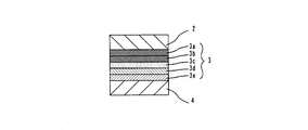
- FIG. 1 is a schematic cross-sectional view schematically showing a configuration of an organic EL element which is an embodiment of the present invention.
- FIG. 2 is a schematic cross-sectional view schematically showing a laminated structure of the organic EL element shown in FIG.
- FIG. 3 is a partial cross-sectional view of an organic EL device according to another embodiment of the present invention.
- FIG. 4 is a partial cross-sectional view of an organic EL device which is still another embodiment of the present invention.
- the organic EL device has a light-transmitting electrode layer 2, an organic layer 3, and a reflective metal electrode layer 4 on a light-transmitting substrate 1. They are stacked in order.
- the metal thin film CF in contact with the organic layer 3 and the plasmon loss preventing dielectric film TF constitute a reflective metal electrode layer 4 as a composite electrode.
- the metal thin film CF functions as a reflective cathode, and the plasmon loss prevention dielectric film TF functions as a plasmon loss prevention unit.
- the translucent material constituting the plasmon loss preventing dielectric film TF laminated on the metal thin film CF is an organic material such as a resin whose refractive index is equal to or higher than the refractive index of the organic layer 3, particularly the organic layer in contact with the metal thin film CF. Selected from materials.
- the plasmon loss preventing dielectric film TF is made of a hole transporting compound.
- “equivalent refractive index” means that the difference between one refractive index and the other refractive index is less than 0.3, preferably 0.2 or less, particularly preferably 0.1 or less. That means. Further, the refractive index “low” or “high” may be “low” or “high” to such an extent that a difference in measurement occurs, but in practice, it exceeds 0.1, preferably exceeds 0.2. More preferably 0.3 or more, still more preferably 0.4 or more, particularly preferably 0.5 or more, indicating a low or high difference.
- a sealing film 5 is formed on the plasmon loss preventing dielectric film TF to cover the organic film 3.
- the sealing film 5 seals the organic layer 3 and protects it from moisture and oxygen in the atmosphere.
- the sealing film 5 is formed of a single layer film such as an inorganic material such as silicon nitride, silicon oxide or silicon nitride carbide, or an organic material such as parylene, or a multilayer film in which an organic material layer and an organic material layer are alternately stacked. Can be done.
- the thickness of the organic layer 3 is set to, for example, 100 nm or more and 5 ⁇ m or less.
- the organic layer 3 sandwiched between the translucent electrode layer 2 and the reflective metal electrode layer is composed of a hole injection layer 3a, a hole transport layer 3b, a light emitting layer 3c, an electron stacked in order. It consists of a transport layer 3d and an electron injection layer 3e.
- the organic layer 3 is a light-emitting laminated body, and is not limited to these laminated structures, and may have a laminated structure including at least a light-emitting layer or a charge transport layer that can also be used.
- the organic layer 3 may be configured by omitting the hole transport layer 3b, the hole injection layer 3a, or the hole injection layer 3a and the electron transport layer 3d from the stacked structure. May be.
- Known methods for forming the organic layer 3 include dry coating methods such as sputtering and vacuum deposition, and wet coating methods such as screen printing, spraying, ink jetting, spin coating, gravure printing, and roll coater. ing.
- dry coating methods such as sputtering and vacuum deposition
- wet coating methods such as screen printing, spraying, ink jetting, spin coating, gravure printing, and roll coater.
- the hole injection layer, the hole transport layer, and the light emitting layer are uniformly formed as a solid film by a wet coating method
- the electron transport layer and the electron injection layer are uniformly formed sequentially as a solid film by a dry coating method.
- a film may be formed.
- all the functional layers may be uniformly and sequentially formed as a solid film by a wet coating method.
- the anode translucent electrode layer 2 for supplying holes to the functional layers up to the light emitting layer 3c is made of ITO (Indium-tin-oxide), ZnO, ZnO—Al 2 O 3 (so-called AZO), In 2 O 3. It can be composed of —ZnO (so-called IZO), SnO 2 —Sb 2 O 3 (so-called ATO), RuO 2 or the like. Furthermore, for the translucent electrode layer 2, it is preferable to select a material having a transmittance of at least 10% at the emission wavelength obtained from the organic EL material.
- the translucent electrode layer 2 usually has a single-layer structure, but it can also have a laminated structure made of a plurality of materials if desired.
- the cathode metal thin film CF that supplies electrons to the functional layers up to the light emitting layer 3c is not limited, but, for example, metals such as aluminum, silver, copper, nickel, chromium, gold, and platinum are used. In addition, these materials may be used only by 1 type and may use 2 or more types together by arbitrary combinations and a ratio.
- the material of the metal thin film CF preferably includes a metal having a low work function in order to perform electron injection efficiently.
- a metal having a low work function for example, an appropriate metal such as tin, magnesium, indium, calcium, aluminum, silver, or an alloy thereof may be used. Used. Specific examples include low work function alloy electrodes such as magnesium-silver alloy, magnesium-indium alloy, and aluminum-lithium alloy.
- the silver thin film with a thickness of 20 nm of the metal thin film CF has a transmittance of 50%.
- An Al film having a thickness of 10 nm as the metal thin film has a transmittance of 50%.
- the 20 nm-thick MgAg alloy film as the metal thin film has a transmittance of 50%.
- the metal thin film CF can be formed as a single layer film or a multilayer film on the organic layer 3 by a sputtering method, a vacuum deposition method or the like.
- the organic layer 3 is sandwiched between and in contact with the translucent electrode layer 2 and the metal thin film CF, the organic layer 3 is interposed between the translucent electrode layer 2 and the metal thin film CF.
- the light generated in the light emitting layer 3c in the organic layer 3 passes through the translucent electrode layer 2, and further passes through the translucent electrode layer 2 after being reflected by the metal thin film CF. Then, it is taken out from the surface of the translucent substrate 1.
- the hole injection layer 3a is preferably a layer containing an electron accepting compound (so-called hole transporting compound).
- the composition for forming a hole injection layer usually contains a hole transporting compound and a solvent as a constituent material of the hole injection layer.
- the solvent include, but are not limited to, ether solvents, ester solvents, aromatic hydrocarbon solvents, amide solvents, and the like.
- ether solvents include aliphatic ethers such as ethylene glycol dimethyl ether, ethylene glycol diethyl ether, propylene glycol monomethyl ether acetate (so-called PGMEA), 1,2-dimethoxybenzene, 1,3-dimethoxybenzene, anisole, and phenetole.
- Aromatic ethers such as 2-methoxytoluene, 3-methoxytoluene, 4-methoxytoluene, 2,3-dimethylanisole, and 2,4-dimethylanisole.
- ester solvent examples include aromatic esters such as phenyl acetate, phenyl propionate, methyl benzoate, ethyl benzoate, propyl benzoate, and n-butyl benzoate.
- aromatic hydrocarbon solvent examples include toluene, xylene, cyclohexylbenzene, 3- isopropylpropylphenyl, 1,2,3,4-tetramethylbenzene, 1,4-diisopropylbenzene, cyclohexylbenzene, methylnaphthalene and the like. Can be mentioned.
- amide solvent examples include N, N-dimethylformamide and N, N-dimethylacetamide.
- dimethyl sulfoxide and the like can also be used. These solvent may use only 1 type and may use 2 or more types by arbitrary combinations and a ratio.
- the hole transporting compound may be a polymer compound such as a polymer or a low molecular compound such as a monomer, but is preferably a low molecular compound.
- the hole transporting compound is preferably a compound having an ionization potential of 4.5 eV to 6.0 eV from the viewpoint of a charge injection barrier from the anode to the hole injection layer.
- hole transporting compounds include aromatic amine derivatives, phthalocyanine derivatives represented by phthalocyanine copper (so-called CuPc), porphyrin derivatives, oligothiophene derivatives, polythiophene derivatives, benzylphenyl derivatives, tertiary amines with fluorene groups.
- Examples include linked compounds, hydrazone derivatives, silazane derivatives, silanamine derivatives, phosphamine derivatives, quinacridone derivatives, polyaniline derivatives, polypyrrole derivatives, polyphenylene vinylene derivatives, polythienylene vinylene derivatives, polyquinoline derivatives, polyquinoxaline derivatives, and carbon.
- the derivative includes, for example, an aromatic amine derivative, and includes an aromatic amine itself and a compound having an aromatic amine as a main skeleton. There may be.
- a conductive polymer obtained by polymerizing 3,4-ethylenedioxythiophene, which is a polythiophene derivative, in high molecular weight polystyrene sulfonic acid is also preferable.
- the end of the polymer of PEDOT / PSS may be capped with methacrylate or the like.
- the hole transporting compound used as the material for the hole injection layer may contain any one of these compounds alone, or may contain two or more.
- the combination is arbitrary, but one or more kinds of aromatic tertiary amine polymer compounds and one or two kinds of other hole transporting compounds.
- an aromatic amine compound is preferable for the hole injection layer, and an aromatic tertiary amine compound is particularly preferable.
- the aromatic tertiary amine compound is a compound having an aromatic tertiary amine structure, and includes a compound having a group derived from an aromatic tertiary amine.
- the concentration of the hole transporting compound in the composition for forming a hole injection layer is usually 0.01% by weight or more, preferably 0.1% by weight or more, and more preferably 0.00% by weight in terms of film thickness uniformity. 5% by weight or more, usually 70% by weight or less, preferably 60% by weight or less, more preferably 50% by weight or less. If this concentration is too high, film thickness unevenness may occur, and if it is too low, defects may occur in the formed hole injection layer.
- the composition for forming a hole injection layer may further contain other components.
- other components include various organic EL materials, binder resins, coatability improvers, and the like.
- only 1 type may be used for another component and it may use 2 or more types together by arbitrary combinations and ratios.
- a material for forming the hole injection layer is mixed with an appropriate solvent to prepare a film-forming composition, and this hole injection layer forming composition
- the hole injection layer is formed by applying the material onto the anode by an appropriate technique, forming a film, and drying.
- the film thickness of the hole injection layer is usually 5 nm or more, preferably 10 nm or more, and usually 1000 nm or less, preferably 500 nm or less.
- the material of the hole transport layer 3b may be any material that has been conventionally used as a constituent material of the hole transport layer.
- it is exemplified as the hole transport compound used in the above-described hole injection layer. Things.
- polyvinylcarbazole derivatives polyarylamine derivatives, polyvinyltriphenylamine derivatives, polyfluorene derivatives, polyarylene derivatives, polyarylene ether sulfone derivatives containing tetraphenylbenzidine, polyarylene vinylene derivatives, polysiloxane derivatives, polythiophenes Derivatives, poly (p-phenylene vinylene) derivatives, and the like.
- These may be any of an alternating copolymer, a random polymer, a block polymer, or a graft copolymer. Further, it may be a polymer having a branched main chain and three or more terminal portions, or a so-called dendrimer.
- a composition for forming a hole transport layer is prepared in the same manner as the formation of the hole injection layer, and then dried after wet film formation.
- the hole transporting layer forming composition contains a solvent.
- the solvent used is the same as that used for the composition for forming the hole injection layer.
- the film forming conditions, the drying conditions, and the like are the same as in the case of forming the hole injection layer.
- the hole transport layer may contain various organic EL materials, a binder resin, a coating property improving agent and the like in addition to the hole transporting compound.
- the film thickness of the hole transport layer is usually 5 nm or more, preferably 10 nm or more, and usually 300 nm or less, preferably 100 nm or less.
- the film thickness of the hole injection layer 3a and / or the hole transport layer 3b from the anode 2 to the light emitting layer 3c is preferably at least 100 nm.
- the light emitting layer 3c may be a red, green and blue light emitting independent light emitting layer or a mixed light emitting layer thereof, a compound having a property of transporting holes (hole transporting compound), or A compound having an electron transporting property (electron transporting compound) can also be contained.
- An organic EL material may be used as a dopant material, and a hole transporting compound, an electron transporting compound, or the like may be appropriately used as a host material. There is no particular limitation on the organic EL material, and a substance that emits light at a desired emission wavelength and has good emission efficiency may be used.
- the organic EL material may be a fluorescent material or a phosphorescent material, but it is preferable to use a phosphorescent material from the viewpoint of internal quantum efficiency.
- the light emitting layer may have a single layer structure or a multilayer structure made of a plurality of materials as desired.
- a fluorescent material may be used for the blue light emitting layer
- a phosphorescent material may be used for the green and red light emitting layers.
- a diffusion preventing layer can be provided between the light emitting layers.
- fluorescent materials blue fluorescent dyes
- examples of fluorescent materials that emit blue light include naphthalene, perylene, pyrene, chrysene, anthracene, coumarin, p-bis (2-phenylethenyl) benzene, and derivatives thereof.
- fluorescent material green fluorescent dye
- examples of the fluorescent material (green fluorescent dye) that emits green light include aluminum complexes such as quinacridone derivatives, coumarin derivatives, and Alq3 (tris (8-hydroxy-quinoline) aluminum).
- Examples of fluorescent materials that give yellow light emission include rubrene and perimidone derivatives.
- red fluorescent dyes examples include DCM (4- (dicyanomethylene) -2-methyl-6- (p-dimethylaminostyryl) -4H-pyran) compounds, benzopyran derivatives, rhodamine derivatives, benzoates. Examples thereof include thioxanthene derivatives and azabenzothioxanthene.
- the phosphorescent material is selected from, for example, the long-period periodic table (hereinafter referred to as the long-period periodic table when referring to “periodic table” unless otherwise specified).
- An organometallic complex containing a metal can be given.
- Preferred examples of the metal selected from Groups 7 to 11 of the periodic table include ruthenium, rhodium, palladium, silver, rhenium, osmium, iridium, platinum, and gold.
- a ligand in which a (hetero) aryl group such as a (hetero) arylpyridine ligand or a (hetero) arylpyrazole ligand and a pyridine, pyrazole, phenanthroline, or the like is connected is preferable.
- a pyridine ligand and a phenylpyrazole ligand are preferable.
- (hetero) aryl represents an aryl group or a heteroaryl group.
- phosphorescent materials include tris (2-phenylpyridine) iridium (so-called Ir (ppy) 3), tris (2-phenylpyridine) ruthenium, tris (2-phenylpyridine) palladium, and bis (2-phenyl).
- Pyridine) platinum tris (2-phenylpyridine) osmium, tris (2-phenylpyridine) rhenium, octaethylplatinum porphyrin, octaphenylplatinum porphyrin, octaethyl palladium porphyrin, octaphenyl palladium porphyrin, and the like.
- the molecular weight of the compound used as the organic EL material is usually 10,000 or less, preferably 5000 or less, more preferably 4000 or less, still more preferably 3000 or less, and usually 100 or more, preferably 200 or more, more preferably 300 or more, still more preferably. Is in the range of 400 or more. If the molecular weight of the organic EL material is too small, the heat resistance will be significantly reduced, gas generation will be caused, the film quality will be deteriorated when the film is formed, or the morphology of the functional layer will be changed due to migration, etc. There is a case. On the other hand, if the molecular weight of the organic EL material is too large, it tends to be difficult to purify the organic compound, or it may take time to dissolve the organic EL material in a solvent when formed by a wet coating method.
- the proportion of the organic EL material in the light emitting layer is usually 0.05% by weight or more and usually 35% by weight or less. If the amount of the organic EL material is too small, uneven light emission may occur, and if the amount is too large, the light emission efficiency may be reduced. In addition, when using together 2 or more types of organic EL material, it is made for the total content of these to be contained in the said range.
- the component having the highest content in the light emitting layer is called a host material, and the component having a smaller content is called a guest material.
- the light emitting layer may contain a hole transporting compound as a constituent material.
- a hole transporting compound examples include various compounds exemplified as the hole transporting compound in the hole injection layer 3a described above, for example, Two or more condensed aromatic rings containing two or more tertiary amines represented by 4′-bis [N- (1-naphthyl) -N-phenylamino] biphenyl (so-called NPB) are attached to the nitrogen atom.
- Aromastituted aromatic diamines aromatic amine compounds having a starburst structure such as 4,4 ′, 4 ′′ -tris (1-naphthylphenylamino) triphenylamine, and aromatics composed of tetramers of triphenylamine And spiro compounds such as 2,2 ′, 7,7′-tetrakis- (diphenylamino) -9,9′-spirobifluorene.
- a hole transportable compound in a light emitting layer, only 1 type may be used for a hole transportable compound, and it may use 2 or more types together by arbitrary combinations and a ratio.
- the proportion of the hole transporting compound in the light emitting layer is usually 0.1% by weight or more and usually 65% by weight or less. If the amount of the hole transporting compound is too small, it may be easily affected by a short circuit, and if it is too large, the film thickness may be uneven. In addition, when using together 2 or more types of hole transportable compounds, it is made for the total content of these to be contained in the said range.
- the light emitting layer may contain an electron transporting compound as a constituent material.
- examples of low molecular weight electron transporting compounds include 2,5-bis (1-naphthyl) -1,3,4-oxadiazole (so-called BND), 2 , 5-bis (6 ′-(2 ′, 2 ′′ -bipyridyl))-1,1-dimethyl-3,4-diphenylsilole (so-called PyPySPyPy), bathophenanthroline (so-called BPhen), 2,9 -Dimethyl-4,7-diphenyl-1,10-phenanthroline (so-called BCP, bathocuproin), 2- (4-biphenylyl) -5- (p-tertiarybutylphenyl) -1,3,4-oxadiazole (So-called tBu-PBD), 4,4′-bis (9H-carbazol-9-yl) biphenyl (so-called BND),
- the proportion of the electron transporting compound in the light emitting layer is usually 0.1% by weight or more and usually 65% by weight or less. If the amount of the electron transporting compound is too small, it may be easily affected by a short circuit, and if it is too large, the film thickness may be uneven. In addition, when using together 2 or more types of electron transport compounds, it is made for the total content of these to be contained in the said range.
- the light emitting layer is prepared by dissolving the above light emitting layer material in an appropriate solvent to prepare a composition for forming a light emitting layer. Is formed. Therefore, in the case of forming by a wet coating method, the light emitting layer coating solution is prepared by dispersing or dissolving at least two kinds of solid contents (host material and guest material) to be the light emitting layer as a solute in a solvent.
- the solvent to be used can be selected from the solvents that can be used for the composition for forming a hole injection layer.
- the ratio of the light emitting layer solvent to the light emitting layer forming composition for forming the light emitting layer is usually 0.01% by weight or more and usually 70% by weight or less.
- the film thickness of the light emitting layer is usually 3 nm or more, preferably 5 nm or more, and usually 200 nm or less, preferably 100 nm or less. If the light emitting layer is too thin, defects may occur in the film, and if it is too thick, the driving voltage may increase.
- the electron transport layer 3d is provided for the purpose of further improving the light emission efficiency of the organic EL element, and efficiently transports electrons injected from the cathode between the electrodes to which an electric field is applied in the direction of the light emitting layer. It is formed from an electron transporting compound capable of forming
- the electron transporting compound used for the electron transporting layer usually, the electron injection efficiency from the cathode conductive film CF or the electron injection layer 3e is high, and the injected electrons with high electron mobility are efficiently used.
- a compound that can be transported is used. Examples of compounds that satisfy such conditions include metal complexes of Alq3 and 10-hydroxybenzo [h] quinoline, oxadiazole derivatives, distyrylbiphenyl derivatives, silole derivatives, 3-hydroxyflavone metal complexes, and 5-hydroxyflavones.
- Metal complex benzoxazole metal complex, benzothiazole metal complex, trisbenzimidazolylbenzene, quinoxaline compound, phenanthroline derivative, 2-t-butyl-9,10-N, N′-dicyanoanthraquinonediimine, n-type hydrogenated amorphous Quality silicon carbide, n-type zinc sulfide, n-type zinc selenide and the like.
- the formation method of the electron transport layer is not limited, and can be formed by a wet coating method or a dry coating method.
- the electron transport layer is prepared by dissolving the electron transport layer material in an appropriate solvent to prepare a composition for forming an electron transport layer. It is formed by removing.
- the solvent to be used can be selected from the solvents that can be used for the composition for forming a hole injection layer.
- the film thickness of the electron transport layer is usually 1 nm or more, preferably 5 nm or more, and usually 300 nm or less, preferably 100 nm or less.
- the electron injection layer 3e plays a role of efficiently injecting electrons injected from the cathode into the electron transport layer and the light emitting layer.
- the electron injection layer 3e includes organic electron transport compounds represented by metal complexes such as nitrogen-containing heterocyclic compounds such as bathophenanthroline and aluminum complexes of 8-hydroxyquinoline. Further, the electron injection efficiency can be increased by doping the electron injection layer 3e of the organic electron transport compound with an electron donating material.
- the electron donating material examples include alkali metals such as sodium and cesium, alkaline earth metals such as barium and calcium, compounds thereof (CsF, Cs 2 CO 3 , Li 2 O, LiF), sodium, Alkali metals such as potassium, cesium, lithium and rubidium are used.
- the thickness of the electron injection layer 3e is usually 5 nm or more, preferably 10 nm or more, and is usually 200 nm or less, preferably 100 nm or less.
- the formation method of the electron injection layer is not limited, and can be formed by a wet coating method or a dry coating method.
- the electron injection layer is prepared by dissolving the electron injection layer material in a suitable solvent to prepare a composition for forming an electron injection layer. It is formed by removing.
- the solvent to be used can be selected from the solvents that can be used for the composition for forming a hole injection layer.
- the distance between the light emitting point and the metal thin film CF functioning as the cathode is optically set to 3 times (odd times) of ⁇ / 4. That is, the light emitting layer 3c is designed so as to have a light emitting surface whose optical distance from the metal thin film CF is an odd multiple of three times or more of 1/4 of the light emission peak wavelength of the light emitting layer 3c.
- ⁇ / 4 140 and the refractive index is 1.8
- ⁇ 3 233
- the distance from the metal thin film CF to the emission center is 233 nm.
- the metal thin film CF is preferably disposed at a position separated from the light emitting surface by a half wavelength or more of the emission peak wavelength of the light emitting layer 3c.
- the refractive index between the light emitting layer side of the metal thin film CF and the outer plasmon loss prevention dielectric film side is equal to or higher, total reflection conditions are not satisfied at all angles within the circle indicated by the broken line, and evanescent light is not generated. There is no plasmon resonance.
- the evanescent light oozes from the high refractive index side to the low refractive index side at the time of total reflection, and the evanescent light oozed from the low refractive index layer with a thin film (thickness below wavelength) has a high refractive index on the outside. It has the property of returning to the original light. Further, the surface plasmon generated by the evanescent light and the light incident from a predetermined angle resonates (plasmon resonance), resulting in a plasmon loss, and the level of the reflected light rapidly decreases. However, no evanescent light is generated in this embodiment.
- light L3 within an obliquely upward critical angle passes through the hole transport layer 3b, the hole injection layer 3a, and the translucent electrode layer 2 as it is.
- Light L4 having a critical angle or more at the interface between the translucent electrode layer 2 and the glass substrate proceeds while repeatedly attenuated total reflection.
- light L5 obliquely below proceeds as it is from the time of light emission and reaches the metal thin film CF. Plasmon resonance is prevented because the plasmon loss preventing dielectric film TF is used. Also in this case, evanescent light is not generated and plasmon resonance does not occur.
- the downward light L6 does not generate evanescent light, and is reflected by the metal thin film CF so that the optical path length is ⁇ / 4. Furthermore, because of the metal reflection at the metal thin film CF, the phase is further shifted by ⁇ , and eventually the light has the same phase as the emitted light. Therefore, because the phase is the same as that of the upward light, they are output in an intensified manner.
- the metal thin film CF is disposed at a position far from the light emitting layer 3c, that is, 3 ⁇ ⁇ / 4, and the plasmon loss preventing dielectric film TF having a refractive index equal to or higher than that of the organic layer on the opposite side of the metal thin film CF. Therefore, it is possible to obtain an effect of reducing loss during light emission and suppressing plasmon loss.
- the cathode when the cathode is composed only of a thin film metal and the outside is made into the atmosphere or inert gas, the cathode emits light in all directions from the light emitting layer having a refractive index of 1.8.
- the light directed toward is totally reflected by the cathode at a critical angle or more in relation to the refractive index of 1.0 outside the cathode, and evanescent light is generated.
- the evanescent light oozes with an amplitude that decreases exponentially in a direction perpendicular to the cathode plane. Then, surface plasmons are excited by evanescent light on the side opposite to the light extraction of the metal cathode.
- the metal thin film CF is Ag
- resonance occurs at a predetermined angle when the film thickness is 20 nm to 80 nm.
- the degree of absorption differs depending on the film thickness, and the absorption is greatest when the film thickness is about 50 nm.
- the film thickness is 20 nm or less, polarization is not sufficient and incident light is transmitted.
- a dielectric plasmon loss prevention dielectric film TF is laminated on an Ag metal thin film CF having a thickness of 50 nm to prevent generation of surface plasmon by Ag absorption and resonance with evanescent light. .
- the refractive index of the plasmon loss preventing dielectric film TF equal to or higher than the refractive index of the light emitting layer, total reflection by the metal-dielectric material does not occur and evanescent light does not occur.
- the light from the metal thin film CF is reflected and can be extracted without plasmon loss.
- FIG. 4 shows a partial cross-sectional view of the organic EL element according to the second embodiment.
- symbol as the said Example is the same as that of the organic EL element of the said Example, those description is abbreviate
- the plasmon loss prevention dielectric film TF is laminated on the metal thin film CF on the side opposite to the light extraction to prevent plasmon resonance.
- the metal thin film CF can be configured as a multilayer.
- the cathode in contact with the organic layer 3 is composed of two layers, for example, a thin Ag metal thin film main body CF1 and an Al protective metal film CF2 laminated thereon, and further a protective metal film CF2 A plasmon loss preventing dielectric film TF is laminated thereon.
- the protective metal film CF2 is set to a thickness at which evanescent light attenuates.
- the Ag metal thin film main body CF1 has a film thickness of 20 nm to 80 nm, the influence of plasmon resonance starts to appear at the film thickness of 20 nm, and the maximum is the metal thin film main body CF1 per 50 nm of film thickness. Since the thickness at which the plasmon resonance is considerably reduced is 80 nm, the minimum value of the total thickness of the metal thin film main body CF1 is 80 nm.
- the range in which the evanescent light on the dielectric TF side of the surface plasmon reaches is also about 300 nm, and it is preferable that the total film thickness of the metal thin film body CF1 and the protective metal film CF2 in which the influence change is reduced is, for example, up to 200 nm. .
- the amplitude of the surface plasmon attenuates exponentially, but the attenuation distance (distance that becomes 1 / e of the amplitude) attenuates more rapidly on the metal side than on the dielectric side.
- the film thickness of the metal thin film body CF1 can be made thinner than the film thickness of the protective metal film CF2.
- the resin solvent may adversely affect the organic material of the organic layer 3, but according to the second embodiment, the protective metal film CF2 is formed. Since it is installed between the metal thin film body CF1 and the plasmon loss preventing dielectric film TF, the influence can be mitigated.
- the protective metal film CF2 in contact with the cathode for example, the Ag metal thin film body CF1 can be made of low-cost Al, Mg, Cr, or the like. Therefore, since the metal thin film main body can be made thin, an organic EL element that does not cause plasmon loss while maintaining performance at low cost can be provided. In addition, since no current flows through the protective metal film CF2, there is no fear of contact with different metals and corrosion in a corrosive environment. In the case of this configuration, the protective metal film CF2 may be grounded.
- a quartz or glass plate, a metal plate or metal foil, a bent resin substrate, a plastic film, a sheet, or the like is used as the translucent substrate 1.
- a glass plate or a transparent plate made of a synthetic resin such as polyester, polymethacrylate, polycarbonate, or polysulfone is preferable.
- a synthetic resin substrate it is necessary to pay attention to gas barrier properties. If the gas barrier property of the substrate is too small, the organic EL element may be deteriorated by the outside air that has passed through the substrate. Therefore, a method of securing a gas barrier property by providing a dense silicon oxide film or the like on at least one surface of the synthetic resin substrate is also a preferable method.
- the organic layer is a light emitting laminate, but the light emitting laminate can also be configured by lamination of inorganic material films.
Abstract
有機エレクトロルミネッセンス素子は、光取り出し側の透光性電極層及び反射金属電極層の間に挟持され発光層を含む有機層を含む。反射金属電極層は、有機層に接する金属薄膜と、金属薄膜の光取り出し側とは逆側にて金属薄膜に接するプラズモン損失防止誘電体膜と、を有する。
Description
本発明は、有機エレクトロルミネッセンス素子に関する。
透明なガラス基板上の陽極と陰極の電極層の間に発光層を含む有機層が挟持された有機エレクトロルミネッセンス素子(以下、有機EL素子と称する)が知られている(例えば特許文献1~3、参照)。特許文献1には、陰極のピンホール対策のため陰極Al膜厚を100~200nmにするという提案が出されている。特許文献2には、放熱特性改善のためAg合金などの陰極厚みを0.2ミクロンから10ミクロンにするという提案が出されている。特許文献3には、短絡リペア対策のためAlやMgAg合金の陰極を70~90nmにするという提案が出されている。
NATURE|Vol459|14|May 2009
有機EL素子においては、陽極と陰極の間に電圧を印加すると発光層が発光する。発光光は陽極を透明とすることにより陽極とガラス基板を介して取り出される。
ところが、発光層から発せられた光は陽極-ガラス界面間及びガラス-空気界面間での全反射により閉じ込められて消衰する故に、発光層で生成された光のうち約20%程度の光しか外部に取り出すことができない光損失問題がある。これに対して、例えば、Ag陰極と発光層との間の電子輸送層の厚みを厚くして、光損失の1つであるプラズモン損失を抑えることとした有機EL素子も発表されている(例えば非特許文献1参照)。
このように、最近は陰極として反射率の高いAgを使用するようになっている。しかし、特許文献1~3や非特許文献1の従来技術では、陰極の膜厚はあまり重要視されず、材料コストを考慮した陰極構造を提案していない。特許文献1~3にはプラズモン損失に関する記載がない。特許文献1~3や非特許文献1の従来技術では、陰極が単一金属による構成であり、発光層や電子輸送層に接する金属の膜厚が100nmあり、陰極金属を多く消費している。例えば、有機EL素子を照明パネルに適用した場合、陰極はパネル全面に構成されるため、Agなど貴金属を陰極に適用すると、資源の大量消費につながる問題となる。
本発明は、上記した点に鑑みてなされたものであり、プラズモン共鳴による損失を起こさないようにすることができる有機エレクトロルミネッセンス素子を提供することを目的とする。
本発明の有機エレクトロルミネッセンス素子は、透光性電極層及び反射金属電極層の間に挟持されて発光層を含む有機層を含む有機エレクトロルミネッセンス素子であって、
前記反射金属電極層は、前記有機層に接する金属薄膜と、前記有機層と共に前記金属薄膜を挟むプラズモン損失防止誘電体膜と、を有することを特徴とする。
前記反射金属電極層は、前記有機層に接する金属薄膜と、前記有機層と共に前記金属薄膜を挟むプラズモン損失防止誘電体膜と、を有することを特徴とする。
以下、本発明の実施例について図面を参照しつつ説明する。
図1に示すように、本発明の第1の実施例である有機EL素子は、透光性基板1上に、透光性電極層2と、有機層3と、反射金属電極層4とが順に積層されて、構成されている。有機層3に接する金属薄膜CFとプラズモン損失防止誘電体膜TFが複合電極として反射金属電極層4を構成している。金属薄膜CFが反射陰極として機能し、プラズモン損失防止誘電体膜TFがプラズモン損失防止部として機能する。
金属薄膜CF上に積層されるプラズモン損失防止誘電体膜TFを構成する透光性材料は、その屈折率が有機層3特に金属薄膜CFに接する有機層の屈折率と同等以上の樹脂などの有機材料から選択される。例えば、プラズモン損失防止誘電体膜TFは正孔輸送性化合物から構成される。
なお、本明細書において、「屈折率が同等」とは、一方の屈折率と他方の屈折率との差が0.3未満、好ましくは0.2以下、とりわけ好ましくは0.1以下であることをいう。また屈折率が「低い」又は「高い」とは、測定上差が生じる程度に「低く」又は「高」ければよいが、実際上は0.1を超えて、好ましくは0.2を超えて、より好ましくは0.3以上、更に好ましくは0.4以上、とりわけ好ましくは0.5以上差があって低い又は高いことを示す。
反射金属電極層4のプラズモン損失防止誘電体膜TF上にはこれと有機層3を覆う封止膜5が形成されている。封止膜5は有機層3を封止しこれを大気の水分や酸素から保護するものである。封止膜5は、例えば窒化シリコン、酸化シリコン又は窒化炭化シリコンなどの無機材料や、パリレンなどの有機材料などの単層膜、又は有機材料層と有機材料層の交互に積層した多層膜から形成され得る。なお、有機層3の厚みは、例えば100nm以上5μm以下に設定されている。
図2に示すように、透光性電極層2と反射金属電極層の間に挟持された有機層3は、順に積層された正孔注入層3a、正孔輸送層3b、発光層3c、電子輸送層3d及び電子注入層3eからなる。有機層3は発光積層体であり、これら積層構成に限定されることなく、少なくとも発光層を含み、或いは兼用できる電荷輸送層を含む積層構成であってもよい。有機層3は、上記積層構造から正孔輸送層3bを省いて構成しても、正孔注入層3aを省いて構成しても、正孔注入層3aと電子輸送層3dを省いて構成してもよい。
有機層3を成膜する手法として、スパッタリング法や真空蒸着法などの乾式塗布法や、スクリーン印刷、スプレー法、インクジェット法、スピンコート法、グラビア印刷、ロールコータ法などの湿式塗布法が知られている。例えば、正孔注入層、正孔輸送層、発光層を湿式塗布法でベタ膜として均一に成膜して、電子輸送層及び電子注入層を、それぞれ乾式塗布法でベタ膜として均一に順次成膜してもよい。また、すべての機能層を湿式塗布法でベタ膜として均一に順次成膜してもよい。
発光層3cまでの機能層に正孔を供給する陽極の透光性電極層2は、ITO(Indium-tin-oxide)やZnO、ZnO-Al2O3(所謂、AZO)、In2O3-ZnO(所謂、IZO)、SnO2-Sb2O3(所謂、ATO)、RuO2などにより構成され得る。さらに、透光性電極層2は、有機EL材料から得られる発光波長において少なくとも10%以上の透過率を持つ材料を選択することが好ましい。
透光性電極層2は通常は単層構造であるが、所望により複数の材料からなる積層構造とすることも可能である。
発光層3cまでの機能層に電子を供給する陰極の金属薄膜CFには、限定されないが、例えば、アルミニウム、銀、銅、ニッケル、クロム、金、白金などの金属が使われる。なお、これらの材料は、1種のみで用いてもよく、2種以上を任意の組み合わせ及び比率で併用してもよい。
金属薄膜CFの材料としては、効率良く電子注入を行う為に仕事関数の低い金属が含まれること好ましく、例えば、スズ、マグネシウム、インジウム、カルシウム、アルミニウム、銀などの適当な金属又はそれらの合金が用いられる。具体例としては、マグネシウム-銀合金、マグネシウム-インジウム合金、アルミニウム-リチウム合金などの低仕事関数合金電極が挙げられる。金属薄膜CFの膜厚20nmの銀薄膜は透過率50%を有する。同金属薄膜としての膜厚10nmのAl膜は透過率50%を有する。同金属薄膜としての膜厚20nmのMgAg合金膜は透過率50%を有する。なお、金属薄膜で金属薄膜CFを構成する場合、その膜厚の下限値は5nmあれば導電性を確保することができる。
金属薄膜CFはスパッタ法や真空蒸着法などにより有機層3上に、単層膜、又は多層膜として形成され得る。
この有機EL素子においては、有機層3は透光性電極層2及び金属薄膜CFの間に接して挟持されている故に、透光性電極層2と金属薄膜CFとを介して有機層3に駆動電圧が印加されることにより、有機層3内の発光層3cにおいて生成された光は透光性電極層2を通過して、さらに金属薄膜CFで反射した後に透光性電極層2を通過して透光性基板1の表面から取り出される。
[有機層3の機能層]
[正孔注入層]
正孔注入層3aは、電子受容性化合物(所謂、正孔輸送性化合物)を含有する層とすることが好ましい。
[正孔注入層]
正孔注入層3aは、電子受容性化合物(所謂、正孔輸送性化合物)を含有する層とすることが好ましい。
湿式塗布法で形成する場合、正孔注入層形成用組成物は通常、正孔注入層の構成材料として正孔輸送性化合物及び溶媒を含有する。溶媒としては、限定されるものではないが、例えば、エーテル系溶媒、エステル系溶媒、芳香族炭化水素系溶媒、アミド系溶媒などが挙げられる。エーテル系溶媒としては、例えば、エチレングリコールジメチルエーテル、エチレングリコールジエチルエーテル、プロピレングリコールモノメチルエーテルアセテート(所謂、PGMEA)などの脂肪族エーテル、1,2-ジメトキシベンゼン、1,3-ジメトキシベンゼン、アニソール、フェネトール、2-メトキシトルエン、3-メトキシトルエン、4-メトキシトルエン、2,3-ジメチルアニソール、2,4-ジメチルアニソールなどの芳香族エーテル、などが挙げられる。
エステル系溶媒としては、例えば、酢酸フェニル、プロピオン酸フェニル、安息香酸メチル、安息香酸エチル、安息香酸プロピル、安息香酸n-ブチルなどの芳香族エステル、などが挙げられる。
芳香族炭化水素系溶媒としては、例えば、トルエン、キシレン、シクロヘキシルベンゼン、3-イロプロピルビフェニル、1,2,3,4-テトラメチルベンゼン、1,4-ジイソプロピルベンゼン、シクロヘキシルベンゼン、メチルナフタレンなどが挙げられる。
アミド系溶媒としては、例えば、N,N-ジメチルホルムアミド、N,N-ジメチルアセトアミド、などが挙げられる。その他、ジメチルスルホキシド、なども用いることができる。これらの溶媒は1種のみを用いてもよく、2種以上を任意の組み合わせ及び比率で用いてもよい。
正孔輸送性化合物は、重合体などの高分子化合物であっても、単量体などの低分子化合物であってもよいが、低分子化合物であることが好ましい。
正孔輸送性化合物としては、陽極から正孔注入層への電荷注入障壁の観点から4.5eV~6.0eVのイオン化ポテンシャルを有する化合物が好ましい。正孔輸送性化合物の例としては、芳香族アミン誘導体、フタロシアニン銅(所謂、CuPc)に代表されるフタロシアニン誘導体、ポルフィリン誘導体、オリゴチオフェン誘導体、ポリチオフェン誘導体、ベンジルフェニル誘導体、フルオレン基で3級アミンを連結した化合物、ヒドラゾン誘導体、シラザン誘導体、シラナミン誘導体、ホスファミン誘導体、キナクリドン誘導体、ポリアニリン誘導体、ポリピロール誘導体、ポリフェニレンビニレン誘導体、ポリチエニレンビニレン誘導体、ポリキノリン誘導体、ポリキノキサリン誘導体、カーボンなどが挙げられる。ここで誘導体とは、例えば、芳香族アミン誘導体を例にするならば、芳香族アミンそのもの及び芳香族アミンを主骨格とする化合物を含むものであり、重合体であっても、単量体であってもよい。
また、正孔輸送性化合物としては、ポリチオフェンの誘導体である3,4-エチレンジオキシチオフェンを高分子量ポリスチレンスルホン酸中で重合してなる導電性ポリマー(所謂、PEDOT/PSS)もまた好ましい。さらに、PEDOT/PSSのポリマーの末端をメタクリレートなどでキャップしたものであってもよい。
正孔注入層の材料として用いられる正孔輸送性化合物は、このような化合物のうち何れか1種を単独で含有していてもよく、2種以上を含有していてもよい。2種以上の正孔輸送性化合物を含有する場合、その組み合わせは任意であるが、芳香族三級アミン高分子化合物1種又は2種以上と、その他の正孔輸送性化合物1種又は2種以上とを併用することもできる。非晶質性、可視光の透過率の点から、正孔注入層には芳香族アミン化合物が好ましく、特に芳香族三級アミン化合物が好ましい。ここで、芳香族三級アミン化合物とは、芳香族三級アミン構造を有する化合物であって、芳香族三級アミン由来の基を有する化合物も含む。
正孔注入層形成用組成物中の、正孔輸送性化合物の濃度は、膜厚の均一性の点で通常0.01重量%以上、好ましくは0.1重量%以上、さらに好ましくは0.5重量%以上、また、通常70重量%以下、好ましくは60重量%以下、さらに好ましくは50重量%以下である。この濃度が高すぎると膜厚ムラが生じる可能性があり、また、低すぎると成膜された正孔注入層に欠陥が生じる可能性がある。
正孔注入層形成用組成物は電子受容性化合物に加えて、さらに、その他の成分を含有させてもよい。その他の成分の例としては、各種の有機EL材料、バインダー樹脂、塗布性改良剤などが挙げられる。なお、その他の成分は、1種のみを用いてもよく、2種以上を任意の組み合わせ及び比率で併用してもよい。
湿式塗布法により正孔注入層を形成する場合、通常は、正孔注入層を構成する材料を適切な溶媒と混合して成膜用の組成物を調製し、この正孔注入層形成用組成物を適切な手法により、陽極上に塗布して成膜し、乾燥することにより正孔注入層を形成する。
正孔注入層の膜厚は、通常5nm以上、好ましくは10nm以上、また、通常1000nm以下、好ましくは500nm以下の範囲である。
[正孔輸送層]
正孔輸送層3bの材料としては、従来、正孔輸送層の構成材料として用いられている材料であればよく、例えば、前述の正孔注入層に使用される正孔輸送性化合物として例示したものが挙げられる。また、アリールアミン誘導体、フルオレン誘導体、スピロ誘導体、カルバゾール誘導体、ピリジン誘導体、ピラジン誘導体、ピリミジン誘導体、トリアジン誘導体、キノリン誘導体、フェナントロリン誘導体、フタロシアニン誘導体、ポルフィリン誘導体、シロール誘導体、オリゴチオフェン誘導体、縮合多環芳香族誘導体、金属錯体などが挙げられる。また、例えば、ポリビニルカルバゾール誘導体、ポリアリールアミン誘導体、ポリビニルトリフェニルアミン誘導体、ポリフルオレン誘導体、ポリアリーレン誘導体、テトラフェニルベンジジンを含有するポリアリーレンエーテルサルホン誘導体、ポリアリーレンビニレン誘導体、ポリシロキサン誘導体、ポリチオフェン誘導体、ポリ(p-フェニレンビニレン)誘導体などが挙げられる。これらは、交互共重合体、ランダム重合体、ブロック重合体又はグラフト共重合体のいずれであってもよい。また、主鎖に枝分かれがあり末端部が3つ以上ある高分子や、所謂デンドリマーであってもよい。
正孔輸送層3bの材料としては、従来、正孔輸送層の構成材料として用いられている材料であればよく、例えば、前述の正孔注入層に使用される正孔輸送性化合物として例示したものが挙げられる。また、アリールアミン誘導体、フルオレン誘導体、スピロ誘導体、カルバゾール誘導体、ピリジン誘導体、ピラジン誘導体、ピリミジン誘導体、トリアジン誘導体、キノリン誘導体、フェナントロリン誘導体、フタロシアニン誘導体、ポルフィリン誘導体、シロール誘導体、オリゴチオフェン誘導体、縮合多環芳香族誘導体、金属錯体などが挙げられる。また、例えば、ポリビニルカルバゾール誘導体、ポリアリールアミン誘導体、ポリビニルトリフェニルアミン誘導体、ポリフルオレン誘導体、ポリアリーレン誘導体、テトラフェニルベンジジンを含有するポリアリーレンエーテルサルホン誘導体、ポリアリーレンビニレン誘導体、ポリシロキサン誘導体、ポリチオフェン誘導体、ポリ(p-フェニレンビニレン)誘導体などが挙げられる。これらは、交互共重合体、ランダム重合体、ブロック重合体又はグラフト共重合体のいずれであってもよい。また、主鎖に枝分かれがあり末端部が3つ以上ある高分子や、所謂デンドリマーであってもよい。
湿式塗布法で正孔輸送層を形成する場合は、正孔注入層の形成と同様にして、正孔輸送層形成用組成物を調製した後、湿式成膜後、乾燥させる。
正孔輸送層形成用組成物に、正孔輸送性化合物の他、溶媒を含有する。用いる溶媒は正孔注入層形成用組成物に用いたものと同様である。また、成膜条件、乾燥条件なども正孔注入層の形成の場合と同様である。
正孔輸送層は、正孔輸送性化合物の他、各種の有機EL材料、バインダー樹脂、塗布性改良剤などを含有していてもよい。
正孔輸送層の膜厚は、通常5nm以上、好ましくは10nm以上であり、また通常300nm以下、好ましくは100nm以下である。
上記したように少なくとも正孔注入層3a又は正孔輸送層3bは厚く塗布されることが好ましいので、陽極2から発光層3cまでの正孔注入層3a及び/又は正孔輸送層3bの膜厚の合計は少なくとも100nmであることが好ましい。
[発光層]
発光層3cは赤、緑及び青発光の独立した発光層であってもそれらの混合発光層であってもよい、また、正孔輸送の性質を有する化合物(正孔輸送性化合物)、或いは、電子輸送の性質を有する化合物(電子輸送性化合物)を含有させることもできる。有機EL材料をドーパント材料として使用し、正孔輸送性化合物や電子輸送性化合物などをホスト材料として適宜使用してもよい。有機EL材料については特に限定はなく、所望の発光波長で発光し、発光効率が良好である物質を用いればよい。
発光層3cは赤、緑及び青発光の独立した発光層であってもそれらの混合発光層であってもよい、また、正孔輸送の性質を有する化合物(正孔輸送性化合物)、或いは、電子輸送の性質を有する化合物(電子輸送性化合物)を含有させることもできる。有機EL材料をドーパント材料として使用し、正孔輸送性化合物や電子輸送性化合物などをホスト材料として適宜使用してもよい。有機EL材料については特に限定はなく、所望の発光波長で発光し、発光効率が良好である物質を用いればよい。
有機EL材料としては、任意の公知の材料を適用可能である。例えば、蛍光材料であってもよく、燐光材料であってもよいが、内部量子効率の観点から燐光材料を用いることが好ましい。発光層は単層構造としても、或いは所望により複数の材料からなる多層構造とすることもできる。例えば、青色発光層は蛍光材料を用い、緑色や赤色の発光層は燐光材料を用いるなど、様々な組み合わせで用いてもよい。また、発光層の間に拡散防止層を設けることもできる。
青色発光を与える蛍光材料(青色蛍光色素)としては、例えば、ナフタレン、ペリレン、ピレン、クリセン、アントラセン、クマリン、p-ビス(2-フェニルエテニル)ベンゼン及びそれらの誘導体などが挙げられる。
緑色発光を与える蛍光材料(緑色蛍光色素)としては、例えば、キナクリドン誘導体、クマリン誘導体、Alq3(tris (8-hydroxy-quinoline) aluminum) などのアルミニウム錯体などが挙げられる。
黄色発光を与える蛍光材料(黄色蛍光色素)としては、例えば、ルブレン、ペリミドン誘導体などが挙げられる。
赤色発光を与える蛍光材料(赤色蛍光色素)としては、例えば、DCM(4-(dicyanomethylene)-2-methyl-6-(p-dimethylaminostyryl)-4H-pyran)系化合物、ベンゾピラン誘導体、ローダミン誘導体、ベンゾチオキサンテン誘導体、アザベンゾチオキサンテンなどが挙げられる。
燐光材料としては、例えば、長周期型周期表(以下、特に断り書きの無い限り「周期表」という場合には、長周期型周期表を指すものとする。)第7~11族から選ばれる金属を含む有機金属錯体が挙げられる。周期表第7~11族から選ばれる金属として、好ましくは、ルテニウム、ロジウム、パラジウム、銀、レニウム、オスミウム、イリジウム、白金、金などが挙げられる。錯体の配位子としては、(ヘテロ)アリールピリジン配位子、(ヘテロ)アリールピラゾール配位子などの(ヘテロ)アリール基とピリジン、ピラゾール、フェナントロリンなどが連結した配位子が好ましく、特にフェニルピリジン配位子、フェニルピラゾール配位子が好ましい。ここで、(ヘテロ)アリールとは、アリール基又はヘテロアリール基を表す。
燐光材料として、具体的には、トリス(2-フェニルピリジン)イリジウム(所謂、Ir(ppy)3)、トリス(2-フェニルピリジン)ルテニウム、トリス(2-フェニルピリジン)パラジウム、ビス(2-フェニルピリジン)白金、トリス(2-フェニルピリジン)オスミウム、トリス(2-フェニルピリジン)レニウム、オクタエチル白金ポルフィリン、オクタフェニル白金ポルフィリン、オクタエチルパラジウムポルフィリン、オクタフェニルパラジウムポルフィリンなどが挙げられる。
有機EL材料として用いる化合物の分子量は、通常10000以下、好ましくは5000以下、より好ましくは4000以下、更に好ましくは3000以下、また、通常100以上、好ましくは200以上、より好ましくは300以上、更に好ましくは400以上の範囲である。有機EL材料の分子量が小さ過ぎると、耐熱性が著しく低下したり、ガス発生の原因となったり、膜を形成した際の膜質の低下を招いたり、或いはマイグレーションなどによる機能層のモルフォロジー変化を招来する場合がある。一方、有機EL材料の分子量が大き過ぎると、有機化合物の精製が困難となってしまったり、湿式塗布法で形成する場合の溶媒に溶解させる際に時間を要したりする傾向がある。
なお、有機EL材料は、いずれか1種のみを用いてもよく、2種以上を任意の組み合わせと比率で併用してもよい。発光層における有機EL材料の割合は、通常0.05重量%以上、通常35重量%以下である。有機EL材料が少なすぎると発光ムラを生じる可能性があり、多すぎると発光効率が低下する可能性がある。なお、2種以上の有機EL材料を併用する場合には、これらの合計の含有量が上記範囲に含まれるようにする。発光層における含有量が最も多い成分をホスト材料とより少ない成分をゲスト材料と呼ぶ。
発光層には、その構成材料として、正孔輸送性化合物を含有させてもよい。ここで、正孔輸送性化合物のうち、低分子量の正孔輸送性化合物の例としては、前述の正孔注入層3aにおける正孔輸送性化合物として例示した各種の化合物のほか、例えば、4,4’-ビス[N-(1-ナフチル)-N-フェニルアミノ]ビフェニル(所謂、NPB)に代表される、2個以上の3級アミンを含み2個以上の縮合芳香族環が窒素原子に置換した芳香族ジアミン類や、4,4’,4”-トリス(1-ナフチルフェニルアミノ)トリフェニルアミンなどのスターバースト構造を有する芳香族アミン化合物や、トリフェニルアミンの四量体から成る芳香族アミン化合物や、2,2’,7,7’-テトラキス-(ジフェニルアミノ)-9,9’-スピロビフルオレンなどのスピロ化合物などが挙げられる。
なお、発光層において、正孔輸送性化合物は、1種のみを用いてもよく、2種以上を任意の組み合わせ及び比率で併用してもよい。
発光層における正孔輸送性化合物の割合は、通常0.1重量%以上、通常65重量%以下である。正孔輸送性化合物が少なすぎると短絡の影響を受けやすくなる可能性があり、多すぎると膜厚ムラを生じる可能性がある。なお、2種以上の正孔輸送性化合物を併用する場合には、これらの合計の含有量が上記範囲に含まれるようにする。
発光層には、その構成材料として、電子輸送性化合物を含有させてもよい。ここで、電子輸送性化合物のうち、低分子量の電子輸送性化合物の例としては、2,5-ビス(1-ナフチル)-1,3,4-オキサジアゾール(所謂、BND)や、2,5-ビス(6’-(2’,2”-ビピリジル))-1,1-ジメチル-3,4-ジフェニルシロール(所謂、PyPySPyPy)や、バソフェナントロリン(所謂、BPhen)や、2,9-ジメチル-4,7-ジフェニル-1,10-フェナントロリン(所謂、BCP、バソクプロイン)、2-(4-ビフェニリル)-5-(p-ターシャルブチルフェニル)-1,3,4-オキサジアゾール(所謂、tBu-PBD)や、4,4’-ビス(9H-カルバゾール-9-イル)ビフェニル(所謂、CBP)などが挙げられる。なお、発光層において、電子輸送性化合物は、1種のみを用いてもよく、2種以上を任意の組み合わせ及び比率で併用してもよい。
発光層における電子輸送性化合物の割合は、通常0.1重量%以上、通常65重量%以下である。電子輸送性化合物が少なすぎると短絡の影響を受けやすくなる可能性があり、多すぎると膜厚ムラを生じる可能性がある。なお、2種以上の電子輸送性化合物を併用する場合には、これらの合計の含有量が上記範囲に含まれるようにする。
湿式塗布法で形成する場合、発光層は、上記発光層材料を適切な溶媒に溶解させて発光層形成用組成物を調製し、それを用いて湿式成膜後、乾燥させ、溶媒を除去することにより、形成される。よって、湿式塗布法で形成する場合、発光層塗布液には、発光層となるべき少なくとも2種類の固形分(ホスト材料とゲスト材料)が溶質として溶媒に分散又は溶解されて、調製される。用いる溶媒は正孔注入層形成用組成物に用い得る上記溶媒から選択され得る。
発光層を形成するための発光層形成用組成物に対する発光層用溶媒の比率は、通常0.01重量%以上、通常70重量%以下、である。なお、発光層用溶媒として2種以上の溶媒を混合して用いる場合には、これらの溶媒の合計がこの範囲を満たすようにする。
発光層の膜厚は通常3nm以上、好ましくは5nm以上、また、通常200nm以下、好ましくは100nm以下の範囲である。発光層の膜厚が、薄すぎると膜に欠陥が生じる可能性があり、厚すぎると駆動電圧が上昇する可能性がある。
[電子輸送層]
電子輸送層3dは、有機EL素子の発光効率を更に向上させることを目的として設けられるもので、電界を与えられた電極間において陰極から注入された電子を効率よく発光層の方向に輸送することができる電子輸送性化合物より形成される。
電子輸送層3dは、有機EL素子の発光効率を更に向上させることを目的として設けられるもので、電界を与えられた電極間において陰極から注入された電子を効率よく発光層の方向に輸送することができる電子輸送性化合物より形成される。
電子輸送層に用いられる電子輸送性化合物としては、通常、陰極の導電性膜CF又は電子注入層3eからの電子注入効率が高く、且つ、高い電子移動度を有し注入された電子を効率よく輸送することができる化合物を用いる。このような条件を満たす化合物としては、例えば、Alq3や10-ヒドロキシベンゾ[h]キノリンの金属錯体、オキサジアゾール誘導体、ジスチリルビフェニル誘導体、シロール誘導体、3-ヒドロキシフラボン金属錯体、5-ヒドロキシフラボン金属錯体、ベンズオキサゾール金属錯体、ベンゾチアゾール金属錯体、トリスベンズイミダゾリルベンゼン、キノキサリン化合物、フェナントロリン誘導体、2-t-ブチル-9,10-N,N’-ジシアノアントラキノンジイミン、n型水素化非晶質炭化シリコン、n型硫化亜鉛、n型セレン化亜鉛などが挙げられる。
なお、電子輸送層の材料は、1種のみを用いてもよく、2種以上を任意の組み合わせ及び比率で併用してもよい。
電子輸送層の形成方法に制限はなく、湿式塗布法または乾式塗布法で形成することができる。湿式塗布法で形成する場合、電子輸送層は、上記電子輸送層材料を適切な溶媒に溶解させて電子輸送層形成用組成物を調製し、それを用いて湿式成膜後、乾燥させ、溶媒を除去することにより、形成される。用いる溶媒は正孔注入層形成用組成物に用い得る上記溶媒から選択され得る。
電子輸送層の膜厚は、通常1nm以上、好ましくは5nm以上、また、通常300nm以下、好ましくは100nm以下の範囲である。
[電子注入層]
電子注入層3eは、陰極から注入された電子を効率良く電子輸送層や発光層へ注入する役割を果たす。例えば、電子注入層3eには、バソフェナントロリンなどの含窒素複素環化合物や8-ヒドロキシキノリンのアルミニウム錯体などの金属錯体に代表される有機電子輸送化合物が挙げられる。また、有機電子輸送化合物の電子注入層3eに電子供与性材料をドープすることにより、電子注入効率を高めることができる。電子供与性材料には、例としては、ナトリウムやセシウムなどのアルカリ金属、バリウムやカルシウムなどのアルカリ土類金属、それらの化合物(CsF、Cs2CO3、Li2O、LiF)や、ナトリウム、カリウム、セシウム、リチウム、ルビジウムなどのアルカリ金属などなどが用いられる。電子注入層3eの膜厚は、通常、5nm以上、中でも10nm以上が好ましく、また、通常200nm以下、中でも100nm以下が好ましい。
電子注入層3eは、陰極から注入された電子を効率良く電子輸送層や発光層へ注入する役割を果たす。例えば、電子注入層3eには、バソフェナントロリンなどの含窒素複素環化合物や8-ヒドロキシキノリンのアルミニウム錯体などの金属錯体に代表される有機電子輸送化合物が挙げられる。また、有機電子輸送化合物の電子注入層3eに電子供与性材料をドープすることにより、電子注入効率を高めることができる。電子供与性材料には、例としては、ナトリウムやセシウムなどのアルカリ金属、バリウムやカルシウムなどのアルカリ土類金属、それらの化合物(CsF、Cs2CO3、Li2O、LiF)や、ナトリウム、カリウム、セシウム、リチウム、ルビジウムなどのアルカリ金属などなどが用いられる。電子注入層3eの膜厚は、通常、5nm以上、中でも10nm以上が好ましく、また、通常200nm以下、中でも100nm以下が好ましい。
電子注入層の形成方法に制限はなく、湿式塗布法または乾式塗布法で形成することができる。湿式塗布法で形成する場合、電子注入層は、上記電子注入層材料を適切な溶媒に溶解させて電子注入層形成用組成物を調製し、それを用いて湿式成膜後、乾燥させ、溶媒を除去することにより、形成される。用いる溶媒は正孔注入層形成用組成物に用い得る上記溶媒から選択され得る。
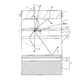
図3を参照しつつ有機EL素子の動作を、発光層3cに560nmを中心ピーク波長(以下λという)とする発光スペクトルの発光材料を用いた場合で説明する。
本実施例において、発光点と陰極とし機能する金属薄膜CFと間の距離は光学的にλ/4の3倍(奇数倍)に設定してある。すなわち、発光層3cは、金属薄膜CFからの光学的距離が発光層3cの発光ピーク波長の1/4の3倍以上の奇数倍である発光面を有するように、設計されている。ここでは、560nmの場合、λ/4=140で屈折率1.8なので、(140/1.8)×3=233となり、金属薄膜CFから発光中心までの距離は233nmである。光の最小ビーム径はλであるので、発光点での光のエネルギー分布の最小径は560nmということができる。発光層を含む有機層の平均屈折率を1.8とすれば、エネルギー分布は物理的には560/1.8=311nm(半径155.5nm)の距離範囲内である。
図3において発光点から半径155.5nmの破線で示す円を重ねてみるとエネルギーの端が、電子注入層3eの中間程に位置し、金属薄膜CFに達していない。すなわち、金属薄膜CFは、発光面から発光層3cの発光ピーク波長の1/2波長分以上離れた位置に配置されていることが好ましい。
金属薄膜CFの発光層側と外側のプラズモン損失防止誘電体膜側との屈折率は同等以上なので、破線で示す円内すべての角度において全反射条件が成立せず、エバネッセント光は発生せず、プラズモン共鳴も起きない。
エバネッセント光は全反射の時の高屈折率側から低屈折率側に染み出し、低屈折率層が薄膜(波長以下膜厚)で染み出したエバネッセント光がその外側の屈折率が高いものがあればもとの光に戻る性質がある。また、エバネッセント光と所定の角度から入射した光により生じる表面プラズモンとが共鳴を起こし(プラズモン共鳴)、プラズモン損失となり、反射光のレベルが急激に減少する。しかし、本実施例ではエバネッセント光は発生しない。
図3において上向きの光L1は金属薄膜CFで反射した光と同じ位相なので、強め合って、ガラス基板1から出力される。
図3において横向きの光L2は発光した時点で、エネルギー分布内に存在するが、全反射条件を満足しないので、そのまま横向きに光は減衰しながら進む。
図3において斜め上向きの臨界角以内の光L3はそのまま正孔輸送層3b、正孔注入層3a及び透光性電極層2を通過する。透光性電極層2及びガラス基板界面で臨界角以上の光L4は全反射を繰り返し減衰しながら進む。
図3において斜め下の光L5は発光時点からそのまま進み、金属薄膜CFへ至る。プラズモン損失防止誘電体膜TFを用いた故に、プラズモン共鳴を防いでいる。この場合もエバネッセント光は発生せず、プラズモン共鳴も生じない。
図3において下向きの光L6もエバネッセント光は生じず、金属薄膜CFで反射され光路長がλ/4なので位相は往復でλ/2ずれる。さらに金属薄膜CFでの金属反射のため、位相がさらにπずれており、結局発光した光と同じ位相の光となっている。よって、上へ向かった光と同位相のため、強め合って出力される。
以上のように、金属薄膜CFを発光層3cから遠い位置すなわち3×λ/4に配置し、金属薄膜CFの反対側に、有機層と同等以上の屈折率を有するプラズモン損失防止誘電体膜TFを設けて構成したので、発光時の損失を減少し、プラズモン損失を抑える効果を得ることができる。
かかるプラズモン損失抑制効果の説明をする。
一般的な有機EL構造の場合、薄膜金属だけで陰極を構成し、その外側が大気や不活性ガスにしたとき、屈折率1.8の発光層で全方向に発光した光のなかで、陰極に向かった光は、陰極の外の屈折率1.0との関係で、臨界角以上で、陰極で全反射し、エバネッセント光が発生する。エバネッセント光は陰極平面に垂直の方向に指数関数的に振幅が減少してにじみ出る。そして、エバネッセント光により、金属陰極の光取り出しとは反対側に表面プラズモンを励起する。
金属陰極の界面への入射光の角度とその膜厚の関係により、エバネッセント光と、表面プラズモンが共鳴を起こすことが知られており、共鳴時、反射はほとんど無くなり、発光素子としては損失となる。
金属薄膜CFがAgの時、膜厚20nm~80nmのときに所定の角度で共鳴がおきる。膜厚によって吸収の度合いが異なり、膜厚50nm程度の時がもっとも吸収が大きい。膜厚20nm以下の時は分極が十分でなく、入射光は透過する。
本実施例では膜厚50nmのAgの金属薄膜CFに誘電体のプラズモン損失防止誘電体膜TFを積層することで、Agの吸収により表面プラズモンの生成を防ぎエバネッセント光との共鳴を防止している。
さらに、プラズモン損失防止誘電体膜TFの屈折率を発光層の屈折率と同等以上にするとことにより、金属-誘電体での全反射も起こらず、エバネッセント光も発生しない。
いずれも、プラズモン共鳴が起こらないので、金属薄膜CFでの光は反射し、プラズモン損失無く取り出すことができる。
図4に第2の実施例である有機EL素子の一部断面図を示す。なお、上記実施例と同一符号で示した構成部分は、上記実施例の有機EL素子と同様であるので、それらの説明は省略する。上記実施例ではAgの金属薄膜CFの単層を設けても、光取り出しの反対側の金属薄膜CF上にプラズモン損失防止誘電体膜TFを積層してプラズモン共鳴を防いでいるが、第2の実施例では金属薄膜CFを多層としても構成できる。
図4に示す第2の実施例では、有機層3に接する陰極を、例えば薄いAgの金属薄膜本体CF1とその上に積層したAlの保護金属膜CF2との2層とし、さらに保護金属膜CF2上にプラズモン損失防止誘電体膜TFを積層している。
保護金属膜CF2はエバネッセント光が減衰する厚みに設定される。例えばAgの金属薄膜本体CF1が膜厚20nm~80nmの場合、プラズモン共鳴の影響が出始めるのが膜厚20nmであり、最大で膜厚50nmあたりの金属薄膜本体CF1である。プラズモン共鳴がかなり少なくなる厚さが80nmなので、金属薄膜本体CF1のトータルの厚みの最小値が80nmである。
一般的に、誘電体-金属-真空のクレッチマン配置の場合、エバネッセント光が届く範囲にて1波長未満で指数関数的に振幅が減少するので表面プラズモンの真空中側の減衰距離が300nm程度である(「表面プラズモンの基礎と応用」J. Plasma Fusion Res. Vol. 84, No. 1 (2008) 10-18)の第15~16頁の式(53)~(55)参照)。よって、表面プラズモンの誘電体TF側のエバネッセント光が届く範囲も300nm程度であり、影響の変化が少なくなる金属薄膜本体CF1と保護金属膜CF2のトータル膜厚を例えば200nmを上限とすることが好ましい。金属-誘電体界面からの距離が離れるにつれて表面プラズモンの振幅は指数関数的に減衰するが、減衰距離(振幅の1/eになる距離)は金属側のほうが誘電体側より急激に減衰する故に、金属薄膜本体CF1の膜厚を保護金属膜CF2の膜厚より薄くすることができる。
また、プラズモン損失防止誘電体膜TFに樹脂を用いた場合、樹脂の溶剤が有機層3の有機材に悪影響を及ぼす可能性があるが、第2の実施例によれば、保護金属膜CF2を金属薄膜本体CF1とプラズモン損失防止誘電体膜TFの間に設置してあるので、当該影響を緩和できる。
第2の実施例によれば、陰極を例えばAgの金属薄膜本体CF1としてもこれに接している保護金属膜CF2をローコストのAl,Mg,Crなどで構成できる。よって、金属薄膜本体を薄くすることができる故に低コストで性能を保ったまま、プラズモン損失を起こさない有機EL素子が提供できる。また、保護金属膜CF2には電流が流れないので、異種金属の接触かつ腐食環境における腐食などの心配がない。この構成の場合、保護金属膜CF2を接地しても良い。
なお、上記の何れの実施例では、透光性基板1として、石英やガラスの板、金属板や金属箔、曲げられる樹脂基板、プラスチックフィルムやシートなどが用いられる。特にガラス板や、ポリエステル、ポリメタクリレート、ポリカーボネート、ポリスルホンなどの合成樹脂の透明板が好ましい。合成樹脂基板を使用する場合にはガスバリア性に留意する必要がある。基板のガスバリア性が小さすぎると、基板を通過した外気により有機EL素子が劣化することがあるので好ましくない。よって、合成樹脂基板の少なくとも片面に緻密なシリコン酸化膜などを設けてガスバリア性を確保する方法も好ましい方法の一つである。
なお、上記の何れの実施例では有機層を発光積層体としているが、無機材料膜の積層によっても発光積層体を構成できる。
1 透光性基板
2 透光性電極層
3 有機層
3a 正孔注入層
3b 正孔輸送層
3c 発光層
3d 電子輸送層
3e 電子注入層
5 封止膜
TF プラズモン損失防止誘電体膜
CF 金属薄膜
2 透光性電極層
3 有機層
3a 正孔注入層
3b 正孔輸送層
3c 発光層
3d 電子輸送層
3e 電子注入層
5 封止膜
TF プラズモン損失防止誘電体膜
CF 金属薄膜
Claims (6)
- 透光性電極層及び反射金属電極層の間に挟持されて発光層を含む有機層を含む有機エレクトロルミネッセンス素子であって、
前記反射金属電極層は、前記有機層に接する金属薄膜と、前記有機層と共に前記金属薄膜を挟むプラズモン損失防止誘電体膜と、を有することを特徴とする有機エレクトロルミネッセンス素子。 - 前記プラズモン損失防止誘電体膜は前記有機層の屈折率と同等以上の屈折率を有することを特徴とする請求項1に記載の有機エレクトロルミネッセンス素子。
- 前記金属薄膜は20nm~80nmの膜厚を有するAg膜を含むことを特徴とする請求項2に記載の有機エレクトロルミネッセンス素子。
- 前記金属薄膜は前記有機層に接するAg膜の金属薄膜本体と前記有機層反対側に上に積層された保護金属膜とを含み、前記保護金属膜は金属薄膜本体と異なる金属であり、前記金属薄膜の合計厚さが80nm~200nmの範囲にあることを特徴とする請求項2に記載の有機エレクトロルミネッセンス素子。
- 前記発光層は、前記金属薄膜からの光学的距離が前記発光層の発光ピーク波長の1/4の3倍以上の奇数倍である発光面を有することを特徴とする請求項2に記載の有機エレクトロルミネッセンス素子。
- 前記封止膜は、前記発光層の発光ピーク波長の1/2波長分以上前記発光面から離れた位置に配置されていることを特徴とする請求項5に記載の有機エレクトロルミネッセンス素子。
Priority Applications (1)
| Application Number | Priority Date | Filing Date | Title |
|---|---|---|---|
| PCT/JP2012/065739 WO2013190656A1 (ja) | 2012-06-20 | 2012-06-20 | 有機エレクトロルミネッセンス素子 |
Applications Claiming Priority (1)
| Application Number | Priority Date | Filing Date | Title |
|---|---|---|---|
| PCT/JP2012/065739 WO2013190656A1 (ja) | 2012-06-20 | 2012-06-20 | 有機エレクトロルミネッセンス素子 |
Publications (1)
| Publication Number | Publication Date |
|---|---|
| WO2013190656A1 true WO2013190656A1 (ja) | 2013-12-27 |
Family
ID=49768285
Family Applications (1)
| Application Number | Title | Priority Date | Filing Date |
|---|---|---|---|
| PCT/JP2012/065739 WO2013190656A1 (ja) | 2012-06-20 | 2012-06-20 | 有機エレクトロルミネッセンス素子 |
Country Status (1)
| Country | Link |
|---|---|
| WO (1) | WO2013190656A1 (ja) |
Cited By (1)
| Publication number | Priority date | Publication date | Assignee | Title |
|---|---|---|---|---|
| JP2016061852A (ja) * | 2014-09-16 | 2016-04-25 | セイコーエプソン株式会社 | 波長変換素子、光源装置、およびプロジェクター |
Citations (8)
| Publication number | Priority date | Publication date | Assignee | Title |
|---|---|---|---|---|
| JPH11220171A (ja) * | 1998-02-02 | 1999-08-10 | Toyoda Gosei Co Ltd | 窒化ガリウム系化合物半導体素子 |
| JP2000243573A (ja) * | 1999-02-18 | 2000-09-08 | Pioneer Electronic Corp | 有機エレクトロルミネッセンス素子とその製造方法 |
| JP2007157514A (ja) * | 2005-12-06 | 2007-06-21 | Sony Corp | 表示装置 |
| JP2008543074A (ja) * | 2005-06-03 | 2008-11-27 | コーニンクレッカ フィリップス エレクトロニクス エヌ ヴィ | 有機エレクトロルミネッセント光源 |
| WO2011043083A1 (ja) * | 2009-10-09 | 2011-04-14 | 出光興産株式会社 | 有機エレクトロルミネッセンス素子 |
| JP2011521423A (ja) * | 2008-05-23 | 2011-07-21 | エルジー・ケム・リミテッド | 有機発光素子およびその製造方法 |
| JP2011198540A (ja) * | 2010-03-18 | 2011-10-06 | Canon Inc | 表示装置 |
| JP2012094812A (ja) * | 2010-09-28 | 2012-05-17 | Toyoda Gosei Co Ltd | Iii族窒化物半導体発光素子の製造方法 |
-
2012
- 2012-06-20 WO PCT/JP2012/065739 patent/WO2013190656A1/ja active Application Filing
Patent Citations (8)
| Publication number | Priority date | Publication date | Assignee | Title |
|---|---|---|---|---|
| JPH11220171A (ja) * | 1998-02-02 | 1999-08-10 | Toyoda Gosei Co Ltd | 窒化ガリウム系化合物半導体素子 |
| JP2000243573A (ja) * | 1999-02-18 | 2000-09-08 | Pioneer Electronic Corp | 有機エレクトロルミネッセンス素子とその製造方法 |
| JP2008543074A (ja) * | 2005-06-03 | 2008-11-27 | コーニンクレッカ フィリップス エレクトロニクス エヌ ヴィ | 有機エレクトロルミネッセント光源 |
| JP2007157514A (ja) * | 2005-12-06 | 2007-06-21 | Sony Corp | 表示装置 |
| JP2011521423A (ja) * | 2008-05-23 | 2011-07-21 | エルジー・ケム・リミテッド | 有機発光素子およびその製造方法 |
| WO2011043083A1 (ja) * | 2009-10-09 | 2011-04-14 | 出光興産株式会社 | 有機エレクトロルミネッセンス素子 |
| JP2011198540A (ja) * | 2010-03-18 | 2011-10-06 | Canon Inc | 表示装置 |
| JP2012094812A (ja) * | 2010-09-28 | 2012-05-17 | Toyoda Gosei Co Ltd | Iii族窒化物半導体発光素子の製造方法 |
Cited By (1)
| Publication number | Priority date | Publication date | Assignee | Title |
|---|---|---|---|---|
| JP2016061852A (ja) * | 2014-09-16 | 2016-04-25 | セイコーエプソン株式会社 | 波長変換素子、光源装置、およびプロジェクター |
Similar Documents
| Publication | Publication Date | Title |
|---|---|---|
| KR102122188B1 (ko) | 유기 전계 발광 소자 및 유기 전계 발광 디바이스 | |
| JP5884213B2 (ja) | 有機電界発光素子の製造方法、有機電界発光素子、有機elディスプレイ及び有機el照明 | |
| JP2015050095A (ja) | 機能層形成用インクの製造方法、有機el素子の製造方法 | |
| JP6046738B2 (ja) | ミラー装置 | |
| JP6062954B2 (ja) | ミラー装置 | |
| JP2009212510A (ja) | 有機電界発光素子、有機elディスプレイおよび有機el照明 | |
| JP2009266814A (ja) | 有機電界発光素子の製造方法、有機電界発光素子、有機elディスプレイ及び有機el照明 | |
| JP5912174B2 (ja) | 有機エレクトロルミネッセンスパネル及びその製造方法 | |
| KR20140112500A (ko) | 유기 전계 발광 소자, 유기 el 조명 및 유기 el 표시 장치 | |
| JP6433963B2 (ja) | ミラー装置 | |
| JP2010209320A (ja) | 有機電界発光素子用組成物、有機電界発光素子の製造方法、有機電界発光素子、有機elディスプレイ及び有機el照明 | |
| WO2012090560A1 (ja) | 有機エレクトロルミネッセンス素子およびその製造方法 | |
| WO2013190656A1 (ja) | 有機エレクトロルミネッセンス素子 | |
| JP5402703B2 (ja) | 有機電界発光素子、有機elディスプレイ、有機el照明及び有機el信号装置 | |
| WO2013150593A1 (ja) | 有機エレクトロルミネッセンスパネル及びその製造方法 | |
| JP6185109B2 (ja) | 有機エレクトロルミネッセンスパネル及びその製造方法 | |
| JP5527105B2 (ja) | 成膜用インク、成膜方法および発光素子の製造方法 | |
| WO2012176276A1 (ja) | 有機電界発光素子 | |
| WO2013190620A1 (ja) | 有機エレクトロルミネッセンス素子 | |
| JP5527104B2 (ja) | 成膜用インク、成膜方法および発光素子の製造方法 | |
| JP6340404B2 (ja) | 発光装置 | |
| JP2010192474A (ja) | 有機電界発光素子、有機elディスプレイ及び有機el照明 | |
| JP2018117035A (ja) | 有機エレクトロルミネッセンス素子 | |
| WO2014073072A1 (ja) | ミラー装置 | |
| JP2010239008A (ja) | 有機電界発光素子、有機elディスプレイ及び有機el照明 |
Legal Events
| Date | Code | Title | Description |
|---|---|---|---|
| 121 | Ep: the epo has been informed by wipo that ep was designated in this application |
Ref document number: 12879413 Country of ref document: EP Kind code of ref document: A1 |
|
| NENP | Non-entry into the national phase |
Ref country code: DE |
|
| 122 | Ep: pct application non-entry in european phase |
Ref document number: 12879413 Country of ref document: EP Kind code of ref document: A1 |
|
| NENP | Non-entry into the national phase |
Ref country code: JP |