WO2013187293A1 - Esd保護装置 - Google Patents
Esd保護装置 Download PDFInfo
- Publication number
- WO2013187293A1 WO2013187293A1 PCT/JP2013/065585 JP2013065585W WO2013187293A1 WO 2013187293 A1 WO2013187293 A1 WO 2013187293A1 JP 2013065585 W JP2013065585 W JP 2013065585W WO 2013187293 A1 WO2013187293 A1 WO 2013187293A1
- Authority
- WO
- WIPO (PCT)
- Prior art keywords
- electrode
- discharge
- esd protection
- input
- sub
- Prior art date
- Legal status (The legal status is an assumption and is not a legal conclusion. Google has not performed a legal analysis and makes no representation as to the accuracy of the status listed.)
- Ceased
Links
Images







Classifications
-
- H—ELECTRICITY
- H02—GENERATION; CONVERSION OR DISTRIBUTION OF ELECTRIC POWER
- H02H—EMERGENCY PROTECTIVE CIRCUIT ARRANGEMENTS
- H02H9/00—Emergency protective circuit arrangements for limiting excess current or voltage without disconnection
- H02H9/04—Emergency protective circuit arrangements for limiting excess current or voltage without disconnection responsive to excess voltage
- H02H9/044—Physical layout, materials not provided for elsewhere
-
- H—ELECTRICITY
- H01—ELECTRIC ELEMENTS
- H01T—SPARK GAPS; OVERVOLTAGE ARRESTERS USING SPARK GAPS; SPARKING PLUGS; CORONA DEVICES; GENERATING IONS TO BE INTRODUCED INTO NON-ENCLOSED GASES
- H01T4/00—Overvoltage arresters using spark gaps
- H01T4/10—Overvoltage arresters using spark gaps having a single gap or a plurality of gaps in parallel
- H01T4/12—Overvoltage arresters using spark gaps having a single gap or a plurality of gaps in parallel hermetically sealed
-
- H—ELECTRICITY
- H01—ELECTRIC ELEMENTS
- H01T—SPARK GAPS; OVERVOLTAGE ARRESTERS USING SPARK GAPS; SPARKING PLUGS; CORONA DEVICES; GENERATING IONS TO BE INTRODUCED INTO NON-ENCLOSED GASES
- H01T4/00—Overvoltage arresters using spark gaps
- H01T4/16—Overvoltage arresters using spark gaps having a plurality of gaps arranged in series
-
- H—ELECTRICITY
- H05—ELECTRIC TECHNIQUES NOT OTHERWISE PROVIDED FOR
- H05K—PRINTED CIRCUITS; CASINGS OR CONSTRUCTIONAL DETAILS OF ELECTRIC APPARATUS; MANUFACTURE OF ASSEMBLAGES OF ELECTRICAL COMPONENTS
- H05K1/00—Printed circuits
- H05K1/02—Details
- H05K1/0213—Electrical arrangements not otherwise provided for
- H05K1/0254—High voltage adaptations; Electrical insulation details; Overvoltage or electrostatic discharge protection ; Arrangements for regulating voltages or for using plural voltages
- H05K1/0257—Overvoltage protection
- H05K1/0259—Electrostatic discharge [ESD] protection
-
- H—ELECTRICITY
- H05—ELECTRIC TECHNIQUES NOT OTHERWISE PROVIDED FOR
- H05K—PRINTED CIRCUITS; CASINGS OR CONSTRUCTIONAL DETAILS OF ELECTRIC APPARATUS; MANUFACTURE OF ASSEMBLAGES OF ELECTRICAL COMPONENTS
- H05K1/00—Printed circuits
- H05K1/02—Details
- H05K1/0213—Electrical arrangements not otherwise provided for
- H05K1/0254—High voltage adaptations; Electrical insulation details; Overvoltage or electrostatic discharge protection ; Arrangements for regulating voltages or for using plural voltages
- H05K1/0257—Overvoltage protection
- H05K1/026—Spark gaps
-
- H—ELECTRICITY
- H05—ELECTRIC TECHNIQUES NOT OTHERWISE PROVIDED FOR
- H05K—PRINTED CIRCUITS; CASINGS OR CONSTRUCTIONAL DETAILS OF ELECTRIC APPARATUS; MANUFACTURE OF ASSEMBLAGES OF ELECTRICAL COMPONENTS
- H05K2201/00—Indexing scheme relating to printed circuits covered by H05K1/00
- H05K2201/02—Fillers; Particles; Fibers; Reinforcement materials
- H05K2201/0203—Fillers and particles
- H05K2201/0206—Materials
- H05K2201/0209—Inorganic, non-metallic particles
-
- H—ELECTRICITY
- H05—ELECTRIC TECHNIQUES NOT OTHERWISE PROVIDED FOR
- H05K—PRINTED CIRCUITS; CASINGS OR CONSTRUCTIONAL DETAILS OF ELECTRIC APPARATUS; MANUFACTURE OF ASSEMBLAGES OF ELECTRICAL COMPONENTS
- H05K2201/00—Indexing scheme relating to printed circuits covered by H05K1/00
- H05K2201/02—Fillers; Particles; Fibers; Reinforcement materials
- H05K2201/0203—Fillers and particles
- H05K2201/0206—Materials
- H05K2201/0224—Conductive particles having an insulating coating
-
- H—ELECTRICITY
- H05—ELECTRIC TECHNIQUES NOT OTHERWISE PROVIDED FOR
- H05K—PRINTED CIRCUITS; CASINGS OR CONSTRUCTIONAL DETAILS OF ELECTRIC APPARATUS; MANUFACTURE OF ASSEMBLAGES OF ELECTRICAL COMPONENTS
- H05K2201/00—Indexing scheme relating to printed circuits covered by H05K1/00
- H05K2201/09—Shape and layout
- H05K2201/09009—Substrate related
- H05K2201/09063—Holes or slots in insulating substrate not used for electrical connections
Definitions
- the discharge start voltage in the sub-discharge portion is higher than the discharge start voltage in the main discharge portion.
- the plurality of input electrodes include a plurality of two input electrodes constituting the sub-discharge section.
- the plurality of sub-discharge units include sub-discharge units arranged at different positions in the other direction.
- a plurality of output electrodes are electrically connected.
- the device body has a cavity. At least one of the main discharge portion and the sub discharge portion is arranged in the cavity.
- the ESD protection device further includes an external electrode.
- the external electrode is arranged on the apparatus main body.
- the external electrode is connected to the input electrode or the output electrode.
- the reliability of an ESD protection device having a plurality of discharge parts can be improved.
- FIG. 1 is a schematic circuit diagram of the ESD protection apparatus according to the first embodiment.
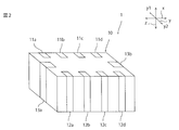
- FIG. 2 is a schematic perspective view of the ESD protection apparatus according to the first embodiment.
- FIG. 3 is a schematic cross-sectional view of the ESD protection apparatus according to the first embodiment.
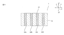
- FIG. 4 is a schematic cross-sectional view of the ESD protection apparatus according to the first embodiment.
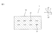
- FIG. 5 is a schematic cross-sectional view of the ESD protection apparatus according to the first embodiment. 6 is a schematic cross-sectional view taken along line VI-VI in FIG.
- FIG. 7 is a schematic cross-sectional view taken along line VII-VII in FIG.
- FIG. 8 is a schematic cross-sectional view of the ESD protection apparatus according to the second embodiment.
- FIG. 9 is a schematic cross-sectional view of the ESD protection apparatus according to the third embodiment.
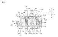
- FIG. 10 is a schematic cross-sectional view of an ESD protection apparatus according to the fourth embodiment.
- FIG. 11 is a schematic cross-sectional view of an ESD protection apparatus according to the fifth embodiment.
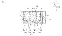
- FIG. 12 is a schematic cross-sectional view of the ESD protection apparatus according to the fifth embodiment.
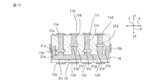
- FIG. 13 is a schematic cross-sectional view of the ESD protection apparatus according to the sixth embodiment.
- FIG. 14 is a schematic cross-sectional view of an ESD protection apparatus according to the sixth embodiment.
- the ESD protection apparatus 1 has a plurality of sets of input terminals and output terminals.
- the ESD protection device 1 has a device body 10.
- the apparatus main body 10 has a substantially rectangular parallelepiped shape.
- the device body 10 is made of an insulating material.
- the apparatus main body 10 can be comprised with suitable ceramics, for example.
- the apparatus main body 10 can be composed of, for example, low temperature co-fired ceramics (LTCC) containing Ba, Al, and Si as main components.
- LTCC low temperature co-fired ceramics
- a first electrode layer 21 and a second electrode layer 22 are provided inside the apparatus body 10.
- the input terminal 11a is electrically connected to the input electrode 21a included in the first electrode layer 21 shown in FIG.
- the input terminal 11 b is electrically connected to the input electrode 21 b included in the first electrode layer 21.
- the input terminal 11 c is electrically connected to the input electrode 21 c included in the first electrode layer 21.
- the input terminal 11 d is electrically connected to the input electrode 21 d included in the first electrode layer 21.
- the input electrodes 21a to 21d are spaced apart from each other along the x-axis direction.
- the electrodes appearing in the present embodiment can be made of an appropriate material such as Cu or Cu alloy.
- main discharge portions 31a to 31d have substantially the same configuration, the specific configuration of the main discharge portions 31a to 31d will be described with reference to FIG. 6 in which the main discharge portion 31a is drawn.
- a discharge auxiliary electrode 41 is disposed between the tip portions of the input electrodes 21a to 21d and the tip portions of the output electrodes 21e to 21h.
- the discharge auxiliary electrode 41 has a function of reducing the discharge start voltage. Specifically, by providing the discharge auxiliary electrode 41, in addition to creeping discharge and air discharge, discharge via the discharge auxiliary electrode 41 also occurs. Usually, the creeping discharge, the air discharge, and the discharge via the discharge auxiliary electrode 41 have the lowest starting voltage of the discharge via the discharge auxiliary electrode 41. Therefore, by providing the discharge auxiliary electrode 41, the discharge start voltage in the main discharge portion can be lowered. Therefore, the dielectric breakdown of the ESD protection device 1 can be suppressed. Moreover, the responsiveness of the ESD protection apparatus 1 can be improved by providing the discharge auxiliary electrode 41.
- the metal particles 41a can be made of, for example, Cu or Ni.
- the diameter of the metal particles 41a can be set to about 2 ⁇ m to 3 ⁇ m, for example.
- the coating film of the metal particles 41a can be made of, for example, aluminum oxide.
- the discharge auxiliary electrode 41 may further include insulating particles made of aluminum oxide in addition to the metal particles 41a and the semiconductor ceramic particles 41b.
- the main discharge portions 31 a to 31 d are surrounded by a protective layer 42.
- a protective layer 42 By providing this protective layer 42, it is possible to suppress the components contained in the device body 10 from diffusing into the discharge auxiliary electrode 14. Therefore, it is possible to suppress a decrease in discharge characteristics due to the deterioration of the discharge auxiliary electrode 14.
- the protective layer 42 is preferably made of a ceramic having a sintering temperature higher than that of the ceramic constituting the apparatus main body 10.
- the apparatus body 10 preferably includes at least one selected from the group consisting of alumina, mullite, zirconia, magnesia, and quartz, for example.
- the plurality of input electrodes 21a to 21d are adjacent to each other in the x-axis direction, and include input electrodes 21a to 21d including a sub-discharge portion.
- the sub-discharge part 51a is provided between the input electrode 21a and the input electrode 21b adjacent in the x-axis direction.
- a sub-discharge portion 51b is provided between the input electrode 21b and the input electrode 21c adjacent in the x-axis direction.
- a sub-discharge portion 51c is provided between the input electrode 21c and the input electrode 21d adjacent in the x-axis direction.
- the sub-discharge portions 51a to 51c have substantially the same configuration as the main discharge portions 31a to 31d. For this reason, the description relating to the main discharge portions 31a to 31d is applied to the sub-discharge portions 51a to 51c.
- the sub-discharge portion 51a includes a protruding portion 21a1 protruding from the input electrode 21a toward the input electrode 21b, and a protruding portion 21b1 protruding from the input electrode 21b toward the input electrode 21a.
- a discharge auxiliary electrode 41 is provided between the protruding portion 21a1 and the protruding portion 21b1, and the discharge start voltage is lowered.
- the sub-discharge portion 51b includes a protruding portion 21b2 protruding from the input electrode 21b toward the input electrode 21c, and a protruding portion 21c1 protruding from the input electrode 21c toward the input electrode 21b.
- a discharge auxiliary electrode 41 is provided between the protruding portion 21b2 and the protruding portion 21c1, and the discharge start voltage is lowered.
- the sub-discharge portion 51c includes a 21c2 projecting from the input electrode 21c toward the input electrode 21d, and a projecting portion 21d1 projecting from the input electrode 21d toward the input electrode 21c.
- a discharge auxiliary electrode 41 is provided between the protruding portion 21c2 and the protruding portion 21d1, and the discharge start voltage is lowered.
- the discharge part is a part where discharge is preferentially generated when a high voltage is applied.
- the main discharge part is a part where discharge is preferentially generated when a high voltage is applied over the sub-discharge part.
- the discharge start voltage in the sub-discharge portions 51a to 51c is preferably equal to or higher than the discharge start voltage in the main discharge portions 31a to 31d, and more preferably 1, 1 or more times the discharge start voltage in the main discharge portions 31a to 31d. Preferably, it is 1,2 times or more.
- the ESD protection apparatus 1 includes the sub-discharge portions 51a to 51c in addition to the main discharge portions 31a to 31d. For this reason, for example, the discharge start voltage of the main discharge portion 31a becomes too high because the tip of the input electrode or the output electrode is melted due to heat generation at the time of discharge or a crack is generated in the vicinity of the discharge auxiliary electrode. Even in this case, when a high voltage is applied to the input electrode 21a, the sub-discharge portion 51a, the input electrode 21b, the main discharge portion 31b, the output electrode 21f, the electrode 21i, and the ground terminals 13a and 13b are discharged. Therefore, as long as at least one discharge start voltage of the main discharge portions 31a to 31d is kept below a predetermined discharge start voltage, the discharge is suitably performed. Therefore, the ESD protection apparatus 1 has excellent reliability.
- the subdischarge part may be provided between some adjacent input electrodes.
- the sub-discharge part it is not always necessary for the sub-discharge part to have a discharge auxiliary electrode. It is not always necessary that the sub-discharge portion is constituted by the protruding portion provided on the input electrode.
- the protruding portion may not be provided on the input electrode, and the auxiliary discharge portion may be configured by providing a discharge auxiliary electrode between adjacent input electrodes.
- the ESD protection device may be, for example, a two-terminal product, a three-terminal product, or may have five or more terminals.
- FIG. 8 is a schematic cross-sectional view of the ESD protection apparatus according to the second embodiment.
- the distance between the main discharge portions 31a to 31d and the sub discharge portions 51a to 51c is long. Therefore, for example, heat generated in the main discharge portions 31a to 31d is not easily transmitted to the sub discharge portions 51a to 51c. Therefore, the sub-discharge portions 51a to 51c are unlikely to deteriorate due to heat generated by the discharge in the main discharge portions 31a to 31d.
- FIG. 9 is a schematic cross-sectional view of the ESD protection apparatus according to the third embodiment.
- the plurality of output electrodes 21e to 21h may not be electrically connected.
- the output electrode 21e is connected to the ground terminal 13a.
- the output electrode 21f is connected to the ground terminal 13b.
- the output electrode 21g is connected to the ground terminal 13c.
- the output electrode 21h is connected to the ground terminal 13d.
- FIG. 10 is a schematic cross-sectional view of an ESD protection apparatus according to the fourth embodiment.
- the main discharge portions 31a to 31d include main discharge portions arranged at different positions in the y-axis direction. Specifically, the main discharge portions 31a to 31d adjacent in the x-axis direction are arranged at different positions in the y-axis direction. Therefore, heat generated by the discharge in the main discharge portions 31a to 31d is not easily transmitted to the main discharge portion adjacent to the main discharge portion. Therefore, it is possible to suppress the thermal deterioration of the main discharge portions 31a to 31d. Therefore, more excellent reliability can be realized.
- the sub-discharge portions 51a to 51c are arranged linearly along the x-axis direction. However, from the viewpoint of realizing further excellent reliability, the sub-discharge portions adjacent in the x-axis direction are arranged.
- the parts 51a to 51c are preferably arranged at different positions in the y-axis direction.
- FIG. 11 is a schematic cross-sectional view of an ESD protection apparatus according to the fifth embodiment.
- FIG. 12 is a schematic cross-sectional view of the ESD protection apparatus according to the fifth embodiment.
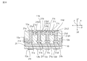
- the main discharge portions 31a to 31d and the sub discharge portions 51a to 51c are provided in different electrode layers. Specifically, the main discharge portions 31 a to 31 d are provided in the first electrode layer 21, and the sub-discharge portions 51 a to 51 c are provided in the second electrode layer 22. This makes it difficult for heat generated when discharge occurs in the main discharge portions 31a to 31d to be transmitted to the sub discharge portions 51a to 51c. Therefore, more excellent reliability can be realized.
- main discharge portions 31a to 31d are arranged so as not to overlap the sub discharge portions 51a to 51c in the height direction of the electrode layer, the heat generated when the discharge occurs in the main discharge portions 31a to 31d is sub discharge.
- the portions 51a to 51c are difficult to be transmitted.
- the cavity 10a is disposed in the same electrode layer by disposing the cavity 10a in different electrode layers. As compared with the case where the insulating layer is formed, peeling of the insulating layer on which the electrode layer is formed can be suppressed. Further, the cavity 10a provided in the main discharge portions 31a to 31d is arranged so as not to overlap the cavity 10a provided in the sub-discharge portions 51a to 51c in the height direction of the electrode layer, thereby providing the cavity 10a. The deformation of the apparatus main body 10 can be suppressed.
- FIG. 13 is a schematic cross-sectional view of an ESD protection apparatus according to the sixth embodiment.
- FIG. 14 is a schematic cross-sectional view of an ESD protection apparatus according to the sixth embodiment.
- the main discharge portions 31a to 31d and the sub discharge portions 51a to 51c are provided in different electrode layers. Specifically, main discharge portions 31 a to 31 d are provided on the first electrode layer 21, and sub-discharge portions 51 a to 51 c are provided on the second electrode layer 22. Further, in the present embodiment, the main discharge portions 31a to 31d adjacent in the x-axis direction are provided at different positions in the y-axis direction.
- sub-discharge portions 51a to 51c adjacent in the x-axis direction are provided at different positions in the y-axis direction. For this reason, the heat generated by the discharge in each discharge part is not easily transmitted by other discharge parts. Therefore, further excellent reliability can be realized.
- the cavity 10a provided in the main discharge portions 31a to 31d and the sub-discharge portions 51a to 51c is in the y-axis direction. Provided at different positions. Also, the cavities 10a provided in the sub-discharge portions 51a to 51c adjacent in the x-axis direction are provided at different positions in the y-axis direction. For this reason, peeling of the insulating layer in which the electrode layer is formed can be suppressed as compared with the case where the cavity 10a is disposed at the same position in the y-axis direction.
Landscapes
- Thermistors And Varistors (AREA)
- Semiconductor Integrated Circuits (AREA)
- Electrostatic Separation (AREA)
Description
図1は、第1の実施形態に係るESD保護装置の略図的回路図である。図2は、第1の実施形態に係るESD保護装置の略図的斜視図である。図3は、第1の実施形態に係るESD保護装置の略図的断面図である。図4は、第1の実施形態に係るESD保護装置の略図的断面図である。図5は、第1の実施形態に係るESD保護装置の略図的断面図である。図6は、図3の線VI-VIにおける略図的断面図である。図7は、図3の線VII-VIIにおける略図的断面図である。
図8は、第2の実施形態に係るESD保護装置の略図的断面図である。図8に示されるESD保護装置では、主放電部31a~31dと、副放電部51a~51cとの間の距離が長い。よって、例えば、主放電部31a~31dにおける発熱が副放電部51a~51cに伝わり難い。よって、主放電部31a~31dにおける放電による発熱により副放電部51a~51cが劣化し難い。
図9は、第3の実施形態に係るESD保護装置の略図的断面図である。図9に示されるESD保護装置のように、複数の出力電極21e~21hは、電気的に接続されていなくてもよい。本実施形態では、出力電極21eがグラウンド端子13aに接続されている。出力電極21fがグラウンド端子13bに接続されている。出力電極21gがグラウンド端子13cに接続されている。出力電極21hがグラウンド端子13dに接続されている。
図10は、第4の実施形態に係るESD保護装置の略図的断面図である。図10に示されるように、本実施形態のESD保護装置では、主放電部31a~31dが、y軸方向において異なる位置に配された主放電部を含む。具体的には、x軸方向において隣り合う主放電部31a~31dが、y軸方向において異なる位置に配されている。よって、主放電部31a~31dにおける放電による発熱が、当該主放電部に隣接する主放電部に伝わり難い。よって、主放電部31a~31dの熱劣化を抑制することができる。従って、より優れた信頼性を実現することができる。なお、本実施形態では、副放電部51a~51cは、x軸方向に沿って直線状に配されているが、さらに優れた信頼性を実現する観点からは、x軸方向において隣り合う副放電部51a~51cが、y軸方向において異なる位置に配されていることが好ましい。
図11は、第5の実施形態に係るESD保護装置の略図的断面図である。図12は、第5の実施形態に係るESD保護装置の略図的断面図である。本実施形態に係るESD保護装置では、主放電部31a~31dと副放電部51a~51cとが異なる電極層に設けられている。具体的には、主放電部31a~31dが第1の電極層21に設けられており、副放電部51a~51cが第2の電極層22に設けられている。このようにすることにより、主放電部31a~31dにおいて放電が生じた際の発熱が副放電部51a~51cに伝わり難くなる。従って、より優れた信頼性を実現することができる。さらに、主放電部31a~31dは副放電部51a~51cと電極層の高さ方向において重ならないように配置されているため、主放電部31a~31dにおいて放電が生じた際の発熱が副放電部51a~51cにより伝わり難くなる。
図13は、第6の実施形態に係るESD保護装置の略図的断面図である。図14は、第6の実施形態に係るESD保護装置の略図的断面図である。本実施形態に係るESD保護装置においても、主放電部31a~31dと副放電部51a~51cとが異なる電極層に設けられている。具体的には、主放電部31a~31dが第1の電極層21に設けられており、副放電部51a~51cが第2の電極層22に設けられている。さらに本実施形態では、x軸方向において隣り合う主放電部31a~31dがy軸方向において異なる位置に設けられている。また、x軸方向において隣り合う副放電部51a~51cがy軸方向において異なる位置に設けられている。このため、各放電部における放電による発熱が他の放電部により伝わり難い。従って、さらに優れた信頼性を実現することができる。
10…装置本体
10a…空洞
11a~11d…入力端子
12a~12d…出力端子
13a~13d…グラウンド端子
21…第1の電極層
21a~21d…入力電極
21a1,21b1,21b2,21c1,21c2,21d1…突出部
21e~21h…出力電極
21i、22a~22d…電極
22…第2の電極層
31a~31d…主放電部
41…放電補助電極
41a…金属粒子
41b…半導体セラミック粒子
42…保護層
51a~51c…副放電部
Claims (11)
- 一の方向に沿って配された複数の入力電極と、
前記一の方向に沿って配されており、前記一の方向に対して傾斜した他の方向において前記入力電極と対向する複数の出力電極と、
を備え、
前記入力電極の前記他の方向における前記出力電極側の端部と、前記出力電極の前記他の方向における前記入力電極側の端部とにより主放電部が構成されており、
前記複数の入力電極は、前記一の方向において隣り合っており、副放電部を構成している2つの入力電極を含む、ESD保護装置。 - 前記2つの入力電極の少なくとも一方の入力電極は、他方の入力電極に向かって突出しており、前記副放電部を構成している突出部を有する、請求項1に記載のESD保護装置。
- 前記2つの入力電極間に配されており、2つの入力電極間の放電開始電圧を低下させる電極であって、前記副放電部を構成している放電補助電極をさらに備える、請求項1または2に記載のESD保護装置。
- 前記副放電部における放電開始電圧が前記主放電部における放電開始電圧よりも高い、請求項1~3のいずれか一項に記載のESD保護装置。
- 前記複数の入力電極は、前記副放電部を構成している2つの入力電極を複数有し、
前記複数の副放電部は、前記他の方向において異なる位置に配された副放電部を含む、請求項1~4のいずれか一項に記載のESD保護装置。 - 前記複数の主放電部は、前記他の方向において異なる位置に配された主放電部を含む、請求項1~5のいずれか一項に記載のESD保護装置。
- 前記入力電極は、前記出力電極と対向している第1の電極層を含む複数の電極層を有し、
前記副放電部は、前記第1の電極層以外の電極層により構成されている、請求項1~6のいずれか一項に記載のESD保護装置。 - 前記複数の出力電極が電気的に接続されている、請求項1~7のいずれか一項に記載のESD保護装置。
- 前記複数の入力電極及び前記複数の出力電極が内部に設けられており、絶縁材料からなる装置本体をさらに備える、請求項1~8のいずれか一項に記載のESD保護装置。
- 前記装置本体は、空洞を有し、
前記主放電部と前記副放電部とのうちの少なくとも一方が前記空洞内に配されている、請求項9に記載のESD保護装置。 - 前記装置本体の上に配されており、前記入力電極または前記出力電極に接続された外部電極をさらに備える、請求項1~10のいずれか一項に記載のESD保護装置。
Priority Applications (3)
| Application Number | Priority Date | Filing Date | Title |
|---|---|---|---|
| JP2014521282A JP5704282B2 (ja) | 2012-06-15 | 2013-06-05 | Esd保護装置 |
| CN201390000549.XU CN204517160U (zh) | 2012-06-15 | 2013-06-05 | Esd保护装置 |
| US14/546,212 US9413168B2 (en) | 2012-06-15 | 2014-11-18 | ESD protection device |
Applications Claiming Priority (2)
| Application Number | Priority Date | Filing Date | Title |
|---|---|---|---|
| JP2012136136 | 2012-06-15 | ||
| JP2012-136136 | 2012-06-15 |
Related Child Applications (1)
| Application Number | Title | Priority Date | Filing Date |
|---|---|---|---|
| US14/546,212 Continuation US9413168B2 (en) | 2012-06-15 | 2014-11-18 | ESD protection device |
Publications (1)
| Publication Number | Publication Date |
|---|---|
| WO2013187293A1 true WO2013187293A1 (ja) | 2013-12-19 |
Family
ID=49758119
Family Applications (1)
| Application Number | Title | Priority Date | Filing Date |
|---|---|---|---|
| PCT/JP2013/065585 Ceased WO2013187293A1 (ja) | 2012-06-15 | 2013-06-05 | Esd保護装置 |
Country Status (4)
| Country | Link |
|---|---|
| US (1) | US9413168B2 (ja) |
| JP (1) | JP5704282B2 (ja) |
| CN (1) | CN204517160U (ja) |
| WO (1) | WO2013187293A1 (ja) |
Families Citing this family (1)
| Publication number | Priority date | Publication date | Assignee | Title |
|---|---|---|---|---|
| WO2021250099A1 (de) * | 2020-06-10 | 2021-12-16 | Tdk Electronics Ag | Überspannungsschutzelement |
Citations (4)
| Publication number | Priority date | Publication date | Assignee | Title |
|---|---|---|---|---|
| JPS61184292U (ja) * | 1985-05-08 | 1986-11-17 | ||
| JPH03276536A (ja) * | 1990-03-27 | 1991-12-06 | Nec Corp | 放電管 |
| JP2005276513A (ja) * | 2004-03-23 | 2005-10-06 | Murata Mfg Co Ltd | サージアブソーバの製造方法 |
| JP2010092779A (ja) * | 2008-10-09 | 2010-04-22 | Mitsubishi Materials Corp | サージアブソーバ及びその製造方法 |
Family Cites Families (2)
| Publication number | Priority date | Publication date | Assignee | Title |
|---|---|---|---|---|
| JP2001143846A (ja) | 1999-11-16 | 2001-05-25 | Tokin Corp | 表面実装型サージアブソーバおよびその製造方法 |
| JP5093345B2 (ja) * | 2008-05-08 | 2012-12-12 | 株式会社村田製作所 | Esd保護機能内蔵基板 |
-
2013
- 2013-06-05 WO PCT/JP2013/065585 patent/WO2013187293A1/ja not_active Ceased
- 2013-06-05 CN CN201390000549.XU patent/CN204517160U/zh not_active Expired - Lifetime
- 2013-06-05 JP JP2014521282A patent/JP5704282B2/ja active Active
-
2014
- 2014-11-18 US US14/546,212 patent/US9413168B2/en active Active
Patent Citations (4)
| Publication number | Priority date | Publication date | Assignee | Title |
|---|---|---|---|---|
| JPS61184292U (ja) * | 1985-05-08 | 1986-11-17 | ||
| JPH03276536A (ja) * | 1990-03-27 | 1991-12-06 | Nec Corp | 放電管 |
| JP2005276513A (ja) * | 2004-03-23 | 2005-10-06 | Murata Mfg Co Ltd | サージアブソーバの製造方法 |
| JP2010092779A (ja) * | 2008-10-09 | 2010-04-22 | Mitsubishi Materials Corp | サージアブソーバ及びその製造方法 |
Also Published As
| Publication number | Publication date |
|---|---|
| JP5704282B2 (ja) | 2015-04-22 |
| JPWO2013187293A1 (ja) | 2016-02-04 |
| US20150070805A1 (en) | 2015-03-12 |
| CN204517160U (zh) | 2015-07-29 |
| US9413168B2 (en) | 2016-08-09 |
Similar Documents
| Publication | Publication Date | Title |
|---|---|---|
| US8711537B2 (en) | ESD protection device and method for producing the same | |
| JP5403370B2 (ja) | Esd保護装置 | |
| US9516728B2 (en) | ESD protection device | |
| JP5954447B2 (ja) | Esd保護装置 | |
| JP2000114005A (ja) | セラミック電子部品 | |
| JP5704282B2 (ja) | Esd保護装置 | |
| JP5874743B2 (ja) | Esd保護装置 | |
| JP5971413B2 (ja) | Esd保護装置 | |
| JP5725262B2 (ja) | Esd保護装置 | |
| JP5757372B2 (ja) | Esd保護デバイス | |
| JP6119371B2 (ja) | Esd保護装置及びその製造方法 | |
| CN117638654A (zh) | 瞬态电压保护器件 | |
| CN106537701B (zh) | Esd保护装置及其制造方法 | |
| JP7792382B2 (ja) | 過渡電圧保護デバイス | |
| JP5760894B2 (ja) | 静電気保護素子 | |
| JP7575352B2 (ja) | 過渡電圧保護デバイス | |
| JP7322925B2 (ja) | 過渡電圧保護デバイス | |
| JP7425976B2 (ja) | 過渡電圧保護デバイス | |
| JP7593888B2 (ja) | 過渡電圧保護デバイス | |
| JP2011071359A (ja) | 配線基板 |
Legal Events
| Date | Code | Title | Description |
|---|---|---|---|
| WWE | Wipo information: entry into national phase |
Ref document number: 201390000549.X Country of ref document: CN |
|
| 121 | Ep: the epo has been informed by wipo that ep was designated in this application |
Ref document number: 13804020 Country of ref document: EP Kind code of ref document: A1 |
|
| ENP | Entry into the national phase |
Ref document number: 2014521282 Country of ref document: JP Kind code of ref document: A |
|
| NENP | Non-entry into the national phase |
Ref country code: DE |
|
| 122 | Ep: pct application non-entry in european phase |
Ref document number: 13804020 Country of ref document: EP Kind code of ref document: A1 |