WO2013175865A1 - 電流センサ - Google Patents
電流センサ Download PDFInfo
- Publication number
- WO2013175865A1 WO2013175865A1 PCT/JP2013/059609 JP2013059609W WO2013175865A1 WO 2013175865 A1 WO2013175865 A1 WO 2013175865A1 JP 2013059609 W JP2013059609 W JP 2013059609W WO 2013175865 A1 WO2013175865 A1 WO 2013175865A1
- Authority
- WO
- WIPO (PCT)
- Prior art keywords
- magnetic
- current sensor
- magnetic core
- core
- hall
- Prior art date
Links
Images


Classifications
-
- G—PHYSICS
- G01—MEASURING; TESTING
- G01R—MEASURING ELECTRIC VARIABLES; MEASURING MAGNETIC VARIABLES
- G01R15/00—Details of measuring arrangements of the types provided for in groups G01R17/00 - G01R29/00, G01R33/00 - G01R33/26 or G01R35/00
- G01R15/14—Adaptations providing voltage or current isolation, e.g. for high-voltage or high-current networks
- G01R15/20—Adaptations providing voltage or current isolation, e.g. for high-voltage or high-current networks using galvano-magnetic devices, e.g. Hall-effect devices, i.e. measuring a magnetic field via the interaction between a current and a magnetic field, e.g. magneto resistive or Hall effect devices
- G01R15/202—Adaptations providing voltage or current isolation, e.g. for high-voltage or high-current networks using galvano-magnetic devices, e.g. Hall-effect devices, i.e. measuring a magnetic field via the interaction between a current and a magnetic field, e.g. magneto resistive or Hall effect devices using Hall-effect devices
-
- G—PHYSICS
- G01—MEASURING; TESTING
- G01R—MEASURING ELECTRIC VARIABLES; MEASURING MAGNETIC VARIABLES
- G01R19/00—Arrangements for measuring currents or voltages or for indicating presence or sign thereof
- G01R19/0092—Arrangements for measuring currents or voltages or for indicating presence or sign thereof measuring current only
-
- G—PHYSICS
- G01—MEASURING; TESTING
- G01R—MEASURING ELECTRIC VARIABLES; MEASURING MAGNETIC VARIABLES
- G01R15/00—Details of measuring arrangements of the types provided for in groups G01R17/00 - G01R29/00, G01R33/00 - G01R33/26 or G01R35/00
- G01R15/14—Adaptations providing voltage or current isolation, e.g. for high-voltage or high-current networks
- G01R15/20—Adaptations providing voltage or current isolation, e.g. for high-voltage or high-current networks using galvano-magnetic devices, e.g. Hall-effect devices, i.e. measuring a magnetic field via the interaction between a current and a magnetic field, e.g. magneto resistive or Hall effect devices
- G01R15/207—Constructional details independent of the type of device used
-
- G—PHYSICS
- G01—MEASURING; TESTING
- G01R—MEASURING ELECTRIC VARIABLES; MEASURING MAGNETIC VARIABLES
- G01R33/00—Arrangements or instruments for measuring magnetic variables
- G01R33/02—Measuring direction or magnitude of magnetic fields or magnetic flux
- G01R33/06—Measuring direction or magnitude of magnetic fields or magnetic flux using galvano-magnetic devices
- G01R33/07—Hall effect devices
- G01R33/072—Constructional adaptation of the sensor to specific applications
Definitions
- the present invention relates to a magnetic proportional type or magnetic balance type current sensor used for current measurement and detection.
- Patent Document 1 is an example of prior art relating to a magnetic proportional current detector.
- the current detector according to the fifth embodiment of Patent Document 1 will be described with reference to FIG.
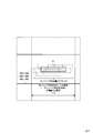
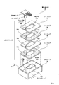
- FIG. 21 is an exploded perspective view showing the current sensor according to the fifth embodiment of Patent Document 1 as components.
- the current detector 90 includes a resin case 92, and a plurality of plate-like sheet cores 94 and 96 are accommodated in the resin case 92 so as to overlap each other. These sheet cores 94 and 96 constitute one magnetic core 98 while being accommodated in the resin case 92. Although two sheet cores 94 and 96 are shown in FIG. 21, the actual number is larger than this, and they are not shown.
- Each of the sheet cores 94 and 96 has a substantially square C shape, and the sheet cores 94 and 96 having such a shape are formed by punching a plate-shaped magnetic material. At that time, each of the sheet cores 94 and 96 is formed with openings 94a and 96a at the center thereof, and gap slits 94b and 96b extending from the openings 94a and 96a toward one side edge.
- the openings 94 a and 96 a are substantially square shapes that match the outer shape of the seat cores 94 and 96.
- the openings 94a and 96a and the gap slits 94b and 96b match each other when viewed in the overlapping direction.
- a continuous through hole is formed at the center position, and a core gap is formed in a part in the circumferential direction. It will be.
- an accommodating portion 92a and a guide sleeve 92b are formed.
- the accommodation portion 92a is open at the top shown in FIG. 21, but a bottom plate 92c is formed below the accommodation portion 92a.
- the guide sleeve 92b extends upward from the bottom plate 92c, and the inside thereof is formed as a hollow current conducting portion 92d.
- the outer shape of the guide sleeve 92b is slightly smaller than the openings 94a and 96a of the seat cores 94 and 96, and the inner dimension of the accommodating portion 92a is larger than the outer shape of the seat cores 94 and 96.
- the openings 94a and 96a are guided along the outer surface of the guide sleeve 92b, so that the seat cores 94 and 96 can be easily positioned relative to each other. It has been done.
- the resin case 92 accommodates the Hall element 10 together with the sheet cores 94 and 96.
- the Hall element 10 is mounted on a circuit board 12, and the circuit board 12 is accommodated so as to be superimposed on the upper surface of the outermost sheet core 96. At this time, the Hall element 10 is positioned in the core gap of the magnetic core 98 by being inserted between the gap slits 94b and 96b of the respective sheet cores 94 and 96.
- the sheet core 96 is a non-oriented silicon steel plate and has a portion (particularly hysteresis width) inferior in magnetic properties as a current detection core, but another sheet core 94 is a permalloy, and is used as a current detection core. Excellent magnetic characteristics (output linearity, hysteresis width, saturation characteristics).
- the magnetic core 98 By forming the magnetic cores 98 by superimposing the sheet cores 94 and 96 made of different magnetic materials on each other, defects inherent to the sheet core 96 can be compensated for by another sheet core 94. As a result, the magnetic core 98 as a whole can exhibit good magnetic characteristics, and can exhibit sufficient characteristics as a product.
- the non-oriented silicon steel plate which is a relatively inexpensive magnetic material
- permalloy which is a relatively expensive magnetic material
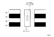
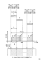
- FIG. 1 is a diagram schematically showing a problem of a current detector using a magnetic core formed by laminating a plurality of conventional materials.
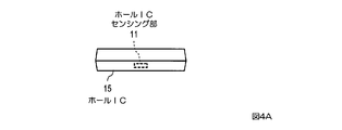
- FIG. 1A is a schematic diagram of the AA cross section in FIG. 21 in a state in which the Hall element 10 is inserted into the core gap of the magnetic core 98.
- FIG. 1B is a schematic diagram for explaining the variation in the total number of magnetic fluxes penetrating through the Hall element sensing unit 11 caused by the position variation of the Hall element sensing unit 11 and the position variation. As shown by a broken line in FIG.
- a Hall element sensing unit 11 that is a region for detecting a magnetic field generated from the magnetic core 98 exists in the Hall element 10.
- the Hall element 10 including the Hall element sensing unit 11 is roughly positioned when the circuit board 12 is accommodated in the accommodating portion 92 a and placed on the uppermost sheet core of the magnetic core 98.
- the inside of the housing portion 92a of the resin case 92 is sealed with a potting resin (not shown).
- the position of the Hall element sensing unit 11 may vary in position as compared with the product as shown by the broken line in FIG. 1B.
- the sheet cores 94 and 96 are made of materials having different magnetic permeability, even if the currents to be measured are equal, the total number of magnetic fluxes penetrating the sensing unit 11 varies between products, and the sensitivity of the current sensor is increased. There was a problem that an error would occur. Further, not only the position variation among products but also the position of the sensing unit 11 may fluctuate due to vibrations applied to the current sensor body during use, thereby changing the sensitivity of the current sensor.
- an object of the present invention is to provide a current sensor that can suppress fluctuations in sensitivity due to variations in the position of a Hall element even when a magnetic core formed by laminating a plurality of materials is used.
- the current sensor of the present invention includes a magnetic core formed in an annular shape with a gap at a part of the circumference, and a magnetic flux that is arranged in the gap and changes according to a current to be measured that passes through a hollow portion of the magnetic core. And a magnetoelectric conversion element for detecting.
- a magnetic core is formed by laminating a plurality of materials in a direction other than the circumferential direction, and is laminated in a region (hereinafter referred to as a sensing unit existence region) predetermined as a region where a sensing unit of a magnetoelectric conversion element can exist. It is characterized in that it is formed so that the magnetic flux density at two points whose direction distances are separated by the length in the stacking direction of the sensing unit is approximate.
- the above-described magnetic core may be formed by irregularly laminating a plurality of materials.
- the above-mentioned magnetic cores may be formed by concentrically laminating.
- the above-described magnetic core may be formed by being laminated in the conduction direction of the current to be measured.
- the above-described magnetic core may be formed by rounding a flat plate in which a plurality of different materials are laminated, and cutting a part of the circumference.
- the magnetic core described above may be formed by alternately laminating directional electromagnetic steel and amorphous magnetic alloy.
- the magnetic core described above may be formed by alternately laminating directional electromagnetic steel and ferrite.
- the perspective view of the magnetic body core with which the current sensor which concerns on the Example of this invention is provided.
- the figure (top view) which shows typically the positional relationship of the magnetic body core with which the current sensor which concerns on the Example of this invention is provided, and a Hall IC sensing part.
- the figure (front view) which shows typically the positional relationship of the magnetic body core with which the current sensor which concerns on the Example of this invention is provided, and a Hall IC sensing part.
- the figure which shows typically the variation in the position of the Hall IC sensing part with which the current sensor which concerns on the Example of this invention is provided.
- FIG. The figure which shows typically the characteristic of magnetic flux density distribution in the gap of the current sensor of Example 2.
- FIG. 3 is a schematic diagram illustrating an application example 1 that can be employed in the current sensor according to the first embodiment.
- FIG. 3 is a schematic diagram illustrating an application example 2 that can be employed in the current sensor according to the first embodiment.
- FIG. 6 is a schematic diagram illustrating an application example 3 that can be employed in the current sensor according to the first embodiment.
- FIG. 6 is a schematic diagram illustrating an application example 4 that can be employed in the current sensor according to the first embodiment.
- FIG. 6 is a schematic diagram illustrating an application example 5 that can be employed in the current sensor according to the first embodiment.
- FIG. 6 is a schematic diagram illustrating an application example 6 that can be employed in the current sensor according to the first embodiment.
- FIG. 6 is a schematic diagram illustrating an application example 7 that can be employed in the current sensor according to the first embodiment.
- FIG. 6 is a schematic diagram showing an application example 8 that can be employed in the current sensor of the first embodiment.
- FIG. 6 is a schematic diagram illustrating an application example 9 that can be employed in the current sensor according to the first embodiment.
- FIG. 10 is a schematic diagram illustrating an application example 10 that can be employed in the current sensor according to the second embodiment.
- FIG. 10 is a schematic diagram illustrating an application example 11 that can be employed in the current sensor according to the second embodiment.
- FIG. 10 is a schematic diagram illustrating an application example 12 that can be employed in the current sensor according to the second embodiment.
- FIG. 10 is a schematic diagram illustrating an application example 13 that can be employed in the current sensor according to the second embodiment.
- FIG. 10 is a schematic diagram showing an application example 14 that can be employed in the current sensor according to the second embodiment.
- FIG. 10 is a schematic diagram illustrating an application example 15 that can be employed in the current sensor according to the second embodiment.
- FIG. 9 is a schematic diagram illustrating an application example 16 that can be employed in the current sensor according to the second embodiment.
- FIG. 9 is a schematic diagram illustrating an application example 17 that can be employed in the current sensor according to the second embodiment.
- FIG. 10 is a schematic diagram illustrating an application example 12 that can be employed in the current sensor according to the second embodiment.
- FIG. 10 is a schematic diagram illustrating an application example 13 that can be employed in the current sensor according to the second embodiment.
- FIG. 10 is a schematic diagram showing an application example 14 that can
- FIG. 10 is a schematic diagram illustrating an application example 18 that can be employed in the current sensor according to the second embodiment.
- FIG. 10 is a schematic diagram illustrating an application example 19 that can be employed in the current sensor according to the third embodiment.
- FIG. 10 is a schematic diagram illustrating an application example 20 that can be employed in the current sensor according to the third embodiment.
- FIG. 10 is a schematic diagram showing an application example 21 that can be employed in the current sensor of the third embodiment.
- FIG. 14 is a schematic diagram showing an application example 22 that can be employed in the current sensor according to the third embodiment.
- FIG. 14 is a schematic diagram showing an application example 23 that can be employed in the current sensor of the third embodiment.
- FIG. 10 is a schematic diagram illustrating an application example 24 that can be employed in the current sensor according to the third embodiment.
- the perspective view shown about the example of the magnetic core which the shape of the magnetic body with which the current sensor of this invention is provided, and the shape which is the variation of the lamination direction were made into the substantially square C shape, and were laminated
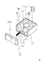
- FIG. 2 is an exploded perspective view of main components of the current sensor according to the embodiment of the present invention.
- FIG. 3 is a perspective view of a magnetic core provided in the current sensor according to the embodiment of the present invention.
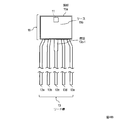
- 4A and 4B are three views of the Hall IC included in the current sensor according to the embodiment of the present invention.
- FIG. 4A is a plan view
- FIG. 4B is a front view
- FIG. 4C is a right side view.
- a current sensor is a device that detects a current flowing in a bus bar or a cable that electrically connects a battery and a device such as a motor in a vehicle such as an electric vehicle or a hybrid vehicle.
- the current sensor according to the embodiment of the present invention includes a magnetic core 100 (101 to 108, 200 to 208, 300 to 305, the reference numeral is properly used for each embodiment described later), a Hall IC 15, A lead wire 13 connected to the Hall IC 15, a case 50, and a lid 60 are provided.
- the magnetic core 100 (101 to 108, 200 to 208, 300 to 305) of the present invention is a soft magnetic material (a material having a small coercive force and a high magnetic permeability, such as iron, silicon steel, permalloy, sendust, permendur, Soft ferrite, amorphous magnetic alloy, nanocrystal magnetic alloy, electromagnetic steel, etc.).
- the electromagnetic steel there are a non-oriented steel plate that is not magnetized by being biased in a specific direction, and a directional steel plate that is easily magnetized only in a specific direction.
- the stacking direction of the plurality of materials may be any direction as long as it is a direction other than the circumferential direction of the core.
- the kind of material may be two kinds, may be three kinds, and may be any kind as long as it is two or more kinds.
- the plurality of materials may be laminated irregularly. Details will be described later.
- the Hall IC 15 provided in the current sensor of the present invention changes according to the current to be measured flowing through the bus bar or cable inserted through the hollow portion 30 of the magnetic core 100 (101 to 108, 200 to 208, 300 to 305).
- the magnetic flux to be detected is detected, and the magnetic flux detection signal is output as an electric signal.
- the Hall IC 15 is connected to an external circuit (not shown) via the lead wire 13.
- the Hall IC 15 may be realized by a combination of a Hall element and an electric circuit.
- the Hall IC 15 and the Hall element are examples of a magnetoelectric conversion element.
- the case 50 has a rectangular parallelepiped box shape, and an upper surface and one side surface are open.
- a cylindrical guide sleeve 52 is provided so as to penetrate the bottom surface 55 of the case 50, and a bus bar or a cable (not shown) can be inserted into the inner cavity (current conducting portion 54) of the guide sleeve 52.
- a stopper 53 that is a plate-like convex portion perpendicular to the outer surface is formed on the outer surface of the guide sleeve 52 adjacent to the opening on the side surface of the case 50.
- a region surrounded by the inner wall of the case 50 and the outer surface of the guide sleeve 52 is referred to as an accommodating portion 51. As shown in FIG.
- the magnetic core 100 (101 to 108, 200 to 208, 300 to 305) has a gap 20 at a part of its circumference and is formed in an annular shape.
- the magnetic core 100 (101 to 108, 200 to 208, 300 to 305) is formed by rounding a plate-like material in an annular shape in the longitudinal direction so as to surround the hollow portion 30, and both ends in the longitudinal direction are interposed via the gap 20. Opposite.
- the outer shape of the guide sleeve 52 is slightly smaller than the hollow part 30 of the magnetic core 100 (101 to 108, 200 to 208, 300 to 305).
- the width of the stopper 53 in the circumferential direction of the guide sleeve 52 is slightly smaller than the width of the gap 20 in the circumferential direction of the core.
- the inner dimension of the accommodating portion 51 is larger than the outer shape of the magnetic core 100 (101 to 108, 200 to 208, 300 to 305). Therefore, when the magnetic core 100 (101 to 108, 200 to 208, 300 to 305) is accommodated in the case 50, the hollow portion 30 and the gap 20 are guided along the outer surfaces of the guide sleeve 52 and the stopper 53.
- the magnetic core 100 (101 to 108, 200 to 208, 300 to 305) is roughly positioned by being placed on the bottom surface 55.
- the Hall IC 15 includes a rectangular parallelepiped case 15b, a magnetoelectric conversion circuit board (not shown) in the case 15b, and a Hall IC sensing unit 11 (the approximate position is indicated by a broken line).
- Five lead wires 13 (13 a, 13 b, 13 c, 13 d, 13 e) are provided at the lower end of the Hall IC 15, and the lead wire 13 is passed through a lead wire hole provided in the oval recess 61 of the lid 60. .
- the central lead wire 13c is provided with a flange portion 13c-1 in which a part of the lead wire 13c is thickened in a hook shape.
- the Hall IC 15 is held with respect to the lid 60 by catching the lead wire hole.
- the lid 60 is attached to the side opening of the case 50. At this time, the end 15a opposite to the end provided with the lead wire 13 of the Hall IC 15 contacts the stopper 53 and is roughly positioned.
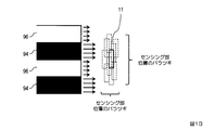
- FIG. 5 is a diagram (plan view) schematically showing a positional relationship between the magnetic core and the Hall IC sensing unit provided in the current sensor according to the embodiment of the present invention.
- FIG. 6 is a diagram (front view) schematically illustrating the positional relationship between the magnetic core and the Hall IC sensing unit included in the current sensor according to the embodiment of the present invention. As shown in FIG.
- the end of the Hall IC sensing unit 11 in the core outer edge direction is referred to as an outer edge direction end 11a
- the end of the Hall IC sensing unit 11 in the core center direction is referred to as a center direction end 11b. I will do it.
- the end of the Hall IC sensing unit 11 in the core upper surface direction is referred to as an upper end 11c
- the end of the Hall IC sensing unit 11 in the core lower surface direction is the lower end 11d. I will call it.
- the positional variation of the Hall IC sensing unit 11 will be described with reference to FIG. As shown in FIG. 7, there is a possibility that the Hall IC sensing unit 11 may vary in position due to the addition of vibrations between products or in use in the core outer edge-center direction and in the core upper surface-lower surface direction. . This is the same as in the case of Patent Document 1.
- a region estimated to be the maximum as the position variation of the Hall IC sensing unit 11 is defined in advance as a sensing unit existence region.
- the sensing unit existence area includes a design value of play generated between the case 50 and the magnetic core 100 (101 to 108, 200 to 208, 300 to 305), a design value of play generated between the lid 60 and the case 50, You may estimate by calculating the largest play which can be theoretically generated from the design value of the play which arises between the lid
- the sensing unit existence region may be set with a margin as a region where the Hall IC sensing unit 11 exists reliably.
- the length in the stacking direction of the sensing portion existence region is represented as S, and is used as a parameter when determining the magnetic flux density distribution of the magnetic core described later.
- the lamination direction of the magnetic core of the present invention may be any direction as long as it is a direction other than the circumferential direction of the core.
- the stacking direction is the core outer edge-center direction. Therefore, in this case, the length S in the stacking direction of the sensing unit existing region is the maximum deviation position in the outer edge direction of the outer edge direction end 11a of the Hall IC sensing unit 11 and the central direction of the center direction end 11b of the Hall IC sensing unit 11 It is determined based on the maximum deviation position.
- the laminating direction is the core upper surface-lower surface direction. Therefore, in this case, the length S in the stacking direction of the sensing unit existence region is the maximum displacement position in the upper direction of the upper end 11c of the Hall IC sensing unit 11 and the lower direction of the lower end 11d of the Hall IC sensing unit 11 It is determined based on the maximum deviation position.
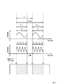
- FIG. 8 is a diagram schematically illustrating the characteristics of the magnetic flux density distribution in the gap of the current sensor according to the first embodiment.
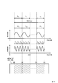
- FIG. 9 is a diagram schematically illustrating the characteristics of the magnetic flux density distribution in the gap of the current sensor according to the second embodiment.
- the coordinates in the stacking direction of the outer edge direction maximum deviation position of the outer edge direction end portion 11a are referred to as EE.
- the coordinate in the stacking direction of the center direction maximum deviation position of the outer edge direction end portion 11a is referred to as EC.
- the coordinates in the stacking direction of the outer edge direction maximum deviation position of the center direction end portion 11b are referred to as CE.
- the coordinate in the stacking direction of the center direction maximum deviation position of the center direction end portion 11b is referred to as CC.
- the coordinate in the stacking direction of the maximum upward shift position of the upper end 11c is referred to as EE.
- the coordinate in the stacking direction of the downward maximum displacement position of the upper end portion 11c is referred to as EC.
- the coordinates in the stacking direction of the upward maximum shift position of the lower end portion 11d are referred to as CE.
- the coordinate in the stacking direction of the downward maximum displacement position of the downward end 11d is referred to as CC.
- the coordinates EE, EC, CE, and CC are used in the same definition in FIG.
- the magnetic flux generated near the right side of the coordinates CE newly penetrates the Hall IC sensing unit 11. Therefore, when the total number of magnetic fluxes penetrating the Hall IC sensing unit 11 is to be kept constant, the magnetic flux density at the coordinates at which the movement of the Hall IC sensing unit 11 does not affect the Hall IC sensing unit 11 and the movement are newly added. It suffices if the magnetic flux density at the coordinates that affect the Hall IC sensing unit 11 is approximate. Specifically, the magnetic flux densities in the vicinity of the coordinates EE and the coordinates CE need only be approximate. Similarly, the magnetic flux densities in the vicinity of the coordinates EC and the coordinates CC need only be approximate. These both corresponding coordinates are spaced a distance L H.
- the section from the left end of the core to the coordinate EE and the section from the coordinate CC to the right end of the core in the figure that do not affect the Hall IC sensing section 11 affects the total number of magnetic fluxes penetrating the Hall IC sensing section 11. No conditions are imposed.
- the magnetic flux generated near the coordinates CE newly penetrates the Hall IC sensing unit 11. Therefore, when the total number of magnetic fluxes penetrating the Hall IC sensing unit 11 is to be kept constant, the magnetic flux density at the coordinates at which the movement of the Hall IC sensing unit 11 does not affect the Hall IC sensing unit 11 and the movement are newly added. It suffices if the magnetic flux density at the coordinates that affect the Hall IC sensing unit 11 is approximate. Specifically, the magnetic flux densities in the vicinity of the coordinates EE and the coordinates CE need only be approximate. These both corresponding coordinates are spaced a distance L H. Up to this point, the process is the same as in FIG. However, in the case of FIG. 9, there is no region where the condition between the coordinates EC and CE existing in FIG. 8 is not imposed.
- section from the left end of the core to the coordinate EE and the section from the coordinate CC to the right end of the core in the figure that do not affect the Hall IC sensing section 11 affects the total number of magnetic fluxes penetrating the Hall IC sensing section 11. No conditions are imposed. This is the same as in FIG.
- the conditions to be satisfied by the magnetic cores 200 to 208 of the current sensor according to the second embodiment described in FIG. 9 are summarized again.
- the magnetic core 200 from 208 of the current sensor of Example 2 with the proviso that the magnetic flux density of the two-point distance in the stacking direction spaced apart by L H in the sensing part presence region is formed so as to approximate.
- the superordinate concept of the present invention described with reference to FIGS. 8 and 9 stipulates that the magnetic flux density at any two points in the region separated by L H is only approximate, and therefore, for example, the coordinate EE in FIG.
- the magnetic flux density distribution in the CC section may be irregular distribution.
- the magnetic flux density distribution from the coordinate EE to the CE section in FIG. 9 may be an irregular distribution.
- FIG. 10 is a schematic diagram schematically showing the regularity of the magnetic flux density distribution of the magnetic core included in the current sensor of the first embodiment.
- FIG. 11 is a diagram schematically illustrating the regularity of the magnetic flux density distribution of the magnetic core included in the current sensor according to the second embodiment.
- the relationship mutually compensating each other by the magnetic flux density of any two points exist in regions spaced L H approximates to suppress the variation in the sensitivity of the current sensor be able to.
- the compensation relationship is established.
- FIG. 12 is a schematic diagram illustrating an application example that can be employed in the current sensor according to the first embodiment.
- 12A is a schematic diagram illustrating the configuration of the magnetic core 100 of Application Example 1
- FIG. 12B is a schematic diagram illustrating the configuration of the magnetic core 101 of Application Example 2
- FIG. 12C illustrates the configuration of the magnetic core 102 of Application Example 3. It is a schematic diagram shown.
- the magnetic core 100 As an application example in which the magnetic core 100 is modified, a material different from the first magnetic body 1 and the second magnetic body 2 (fourth magnetic body) in the section between the coordinates EC and CE, as in the magnetic core 101 of this application example. 4).
- the magnetic core is formed of three kinds of magnetic bodies.
- the section from the left end of the core to the coordinate EE, the section from the coordinate CC to the right end of the core in the figure, and the section from the coordinates EC to CE are formed by laminating a plurality of types of magnetic materials. May be.
- FIG. 13 is a schematic diagram illustrating an application example that can be employed in the current sensor according to the first embodiment.
- 13A is a schematic diagram illustrating the configuration of the magnetic core 103 of Application Example 4
- FIG. 13B is a schematic diagram illustrating the configuration of the magnetic core 104 of Application Example 5
- FIG. 13C illustrates the configuration of the magnetic core 105 of Application Example 6. It is a schematic diagram shown.
- L H spaced magnetic flux density of any two points exist in regions becomes a condition that the approximate not impose any condition from the coordinate EC in magnetic flux density between the CE. Therefore, for example, two kinds of magnetic materials are arranged in an arbitrary pattern between EE and EC, and two kinds of magnetic materials used between EE and EC are arranged between CE and CC. Magnetic materials may be formed by arranging them in the same pattern. As shown in FIG. 13A, in the magnetic core 103 of this application example, the first magnetic body 1 and the third magnetic body 3 are alternately arranged in the sections from the coordinates EE to EC and CE to CC so that the same magnetic flux is obtained. A density distribution is formed.
- this section may have any configuration, such as a magnetic material, a non-magnetic material, and a plurality of types of magnetic materials laminated as in the first to third application examples.
- the first magnetic body 1 and the third magnetic body 3 are alternately arranged in the sections from the coordinates EE to EC and CE to CC, and the same magnetic flux density distribution is formed.
- This is the same as Application Example 4 in that the thicknesses of the first magnetic body 1 and the third magnetic body 3 are different. Specifically, the third magnetic body 3 was formed thinner than the layer of the first magnetic body 1.
- the magnetic core 105 of this application example is formed by alternately arranging two kinds of materials in the section from the coordinates EE to EC and CE to CC, as in the application examples 4 and 5.
- the magnetic core 105 of this application example is formed by alternately laminating magnetic bodies (in the figure, the third magnetic body 3 is shown, but there is no particular limitation on the type of magnetic body) and nonmagnetic bodies 9.
- the magnetic core can also be formed by laminating in an arbitrary pattern using the magnetic material and the non-magnetic material in the sections from the coordinates EE to EC and CE to CC.
- FIG. 14 is a schematic diagram illustrating an application example that can be employed in the current sensor according to the first embodiment.
- 14A is a schematic diagram illustrating the configuration of the magnetic core 106 of Application Example 7
- FIG. 14B is a schematic diagram illustrating the configuration of the magnetic core 107 of Application Example 8
- FIG. 14C illustrates the configuration of the magnetic core 108 of Application Example 9. It is a schematic diagram shown.
- the first magnetic body 1, the second magnetic body 2, and the third magnetic body 3 are arranged in the section from the coordinates EE to EC and CE to CC. , The same magnetic flux density distribution is formed.
- the first magnetic body 1 is formed thicker than the other layers.
- the magnetic core 108 of this application example has four types of magnetic bodies (first magnetic body 1, second magnetic body 2, third magnetic body 3, and fourth magnetic body in the sections from coordinates EE to EC and CE to CC. 4) are arranged to form the same magnetic flux density distribution.
- the application example 7 to the application example 9 show the magnetic core formed by irregularly arranging a plurality of types of magnetic bodies.
- the magnetic core is formed by regularly arranging the magnetic cores. It goes without saying that it is possible. In this case, as described with reference to FIG.
- the fluctuation of the current sensor sensitivity due to the position variation when the Hall IC 15 is disposed in the gap 20 is suppressed. Therefore, it is possible to realize a more accurate current sensor by suppressing variation between products (between operations).
- electromagnetic steel sheets have the disadvantage that high frequency currents of 10 kHz or higher cannot be measured due to iron loss such as eddy current loss, but by forming a magnetic core by combining electromagnetic steel sheets and materials with good frequency characteristics. A current sensor with improved frequency characteristics can be realized.
- ferrite has a demerit that the saturation magnetic flux density is small and the sensor sensitivity is lowered in a large current region, but a magnetic core is formed by laminating ferrite and a directional electrical steel sheet having a high saturation magnetic flux density.
- a current sensor with improved sensitivity in a large current region can be realized.
- Amorphous magnetic alloys have good properties as soft magnetic materials, but have the disadvantage of low mechanical strength, but form a magnetic core by laminating amorphous magnetic alloys and directional electrical steel sheets with high mechanical strength. By doing so, a magnetic core and a current sensor with high mechanical strength can be realized.
- FIG. 15 is a schematic diagram illustrating an application example that can be employed in the current sensor according to the second embodiment.
- 15A is a schematic diagram illustrating the configuration of the magnetic core 200 of Application Example 10
- FIG. 15B is a schematic diagram illustrating the configuration of the magnetic core 201 of Application Example 11
- FIG. 15C illustrates the configuration of the magnetic core 202 of Application Example 12. It is a schematic diagram shown.
- the magnetic flux density of any two points exist in regions spaced L H is that it is the conditions are similar, for example, for inter-CC from the coordinate EE, the magnetic flux density is flat distribution In this way, it is sufficient to configure only one type of magnetic body (first magnetic body 1). Since no condition is imposed on the section of the magnetic core 200 from the left end of the core in the drawing to the coordinate EE, and the section from the coordinate CC to the right end of the core in the drawing, for example, a second magnet different from the first magnetic body 1 is used. A layer of the body 2 may be formed.
- the magnetic core 200 As an application example in which the magnetic core 200 is deformed, a material different from the first magnetic body 1 and the second magnetic body 2 in the section from the coordinate CC to the right end of the core in the figure as in the magnetic core 201 of this application example (The fourth magnetic body 4 may be used.
- the magnetic core is formed of three kinds of magnetic bodies.
- the section from the left end of the core to the coordinate EE and the section from the coordinate CC to the right end of the core in the figure are not magnetic bodies.
- You may comprise a substance (nonmagnetic material 9).
- the section from the core left end in the figure to the coordinate EE and the section from the coordinate CC to the core right end in the figure may be configured by laminating a plurality of types of magnetic materials.
- FIG. 16 is a schematic diagram illustrating an application example that can be employed in the current sensor according to the second embodiment.
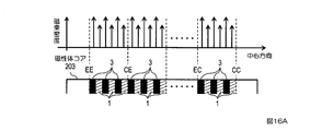
- 16A is a schematic diagram showing the configuration of the magnetic core 203 of the application example 13
- FIG. 16B is a schematic diagram showing the configuration of the magnetic core 204 of the application example 14
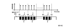
- FIG. 16C shows the configuration of the magnetic core 205 of the application example 15. It is a schematic diagram shown.
- any structure such as a magnetic body, a non-magnetic body, and a stack of a plurality of types of magnetic bodies may be used.
- the thicknesses of the first magnetic body 1 and the third magnetic body 3 are made different from each other.
- the third magnetic body 3 was formed thinner than the layer of the first magnetic body 1.
- the magnetic core 205 of this application example is formed by alternately laminating magnetic bodies (in the figure, the third magnetic body 3 is shown, but there is no particular limitation on the type of magnetic body) and nonmagnetic bodies 9.
- FIG. 17 is a schematic diagram illustrating an application example that can be employed in the current sensor according to the second embodiment.
- 17A is a schematic diagram showing the configuration of the magnetic core 206 of Application Example 16
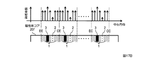
- FIG. 17B is a schematic diagram showing the configuration of the magnetic core 207 of Application Example 17
- FIG. 17C shows the configuration of the magnetic core 208 of Application Example 18. It is a schematic diagram shown.
- the first magnetic body 1 is formed thicker than the other layers.
- the variation in the current sensor products (between operations) is suppressed, and a more accurate current sensor is realized. It is possible to supplement the disadvantages of each material and enjoy the advantages of each material.
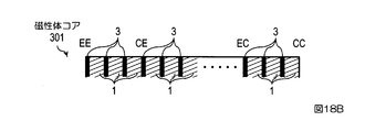
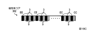
- FIG. 18 is a schematic diagram illustrating an application example that can be employed in the current sensor according to the third embodiment.
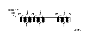
- FIG. 18A to FIG. 18F are schematic views showing the configurations of the magnetic cores 300 to 305 of application examples 19 to 24, respectively.
- the section from the coordinates EE to CC which is the sensing unit existence area set in the second embodiment, to an area including the entire magnetic core.
- the wavelength of the magnetic flux density distribution ⁇ B L H / m (where m is the same) under the condition of S ⁇ 2L H
- the compensation relationship is established as described in FIG. Therefore, in this embodiment, the region from the left end of the core to the right end of the core in the drawing is set as coordinates EE to CC, and the application examples 13 to 18 of the second embodiment are modified to be application examples 19 to 24.
- the magnetic cores 300 to 305 of the current sensor of the present embodiment in addition to the same effects as those of the first and second embodiments, even if the sensing portion existence region is unknown, the condition of S ⁇ 2L H Since the compensation relationship is established, variations in the current sensor between products (operations) can be suppressed.
- Magnetic material> a plurality of types of magnetic bodies are shown as the first magnetic body 1 to the fourth magnetic body 4, but these magnetic bodies are specifically the above-described soft magnetic materials such as iron and silicon steel. , Permalloy, sendust, permendur, soft ferrite (ferrite sheet), amorphous magnetic alloy (amorphous ribbon), nanocrystal magnetic alloy, electromagnetic steel (non-oriented steel sheet, directional steel sheet) and the like.
- a suitable combination in the case of constituting two kinds of magnetic bodies is a magnetic steel plate and a material having good frequency characteristics, a ferrite and a directional magnetic steel plate, an amorphous magnetic alloy and a directional magnetic steel plate, an amorphous magnetic alloy and a ferrite.
- Non-magnetic material Although shown as the nonmagnetic material 9 in Examples 1 to 3, specifically, the nonmagnetic material means a diamagnetic material or a paramagnetic material.
- FIG. 19 is a diagram schematically showing the change in the magnetic flux total number of cases in which the sensing unit stacking direction length L H is not an integer multiple of the wavelength lambda B.
- FIG. 19 shows an example in which two types of magnetic bodies (first magnetic body 1 and third magnetic body 3) are alternately stacked to form a periodic distribution.
- the first thickness of the magnetic substance 1 and L 1, the third thickness of the magnetic body 3 and L 3.
- L 1 > L 3 it is assumed that L 1 > L 3 .
- the aforementioned wavelength ⁇ B L 1 + L 3 .
- the first magnetic permeability of the magnetic substance 1 and mu 1, the third magnetic permeability of the magnetic body 3 and mu 3.
- ⁇ 1 > ⁇ 3 it is assumed that ⁇ 1 > ⁇ 3 .
- ⁇ A ⁇ L ⁇ L 3 >
- ⁇ L is included in the coordinate section where one layer of the first magnetic body 1 exists
- ⁇ L is included in the coordinate section where one layer of the third magnetic body 3 exists.
- the change ⁇ of the total number of magnetic fluxes of the Hall IC sensing unit 11 becomes the largest.
- ⁇ L is included in the coordinate section where one layer of the first magnetic body 1 exists
- ⁇ L is one layer of the third magnetic body 3.
- the change ⁇ in the total number of magnetic fluxes of the Hall IC sensing unit 11 becomes the largest between the case where the Hall IC sensing unit 11 is included in the coordinate section.
- ⁇ C L 3 ⁇ L ⁇ L 1 >
- ⁇ L is included in a coordinate section where one layer of the first magnetic body 1 exists
- ⁇ L is a coordinate section (length L 3) where one layer of the third magnetic body 3 exists.
- the change ⁇ in the total number of magnetic fluxes of the Hall IC sensing unit 11 is the largest.
- ⁇ L is included in the coordinate section where one layer of the first magnetic body 1 exists
- ⁇ L is one layer of the third magnetic body 3.
- the change ⁇ in the total number of magnetic fluxes of the Hall IC sensing unit 11 is the largest between the case where all the coordinate sections (length L 3 ) are included.
- ⁇ E L 1 ⁇ L>
- ⁇ L includes the entire coordinate section (length L 1 ) in which one layer of the first magnetic body 1 exists
- ⁇ L includes the coordinate section in which one layer of the third magnetic body 3 exists (length L 1 ).
- the change ⁇ in the total number of magnetic fluxes of the Hall IC sensing unit 11 is the largest between the case where all the lengths L 3 ) are included.
- L H is precisely not an integral multiple of the wavelength lambda B, even if the excess length ⁇ L occurs, .DELTA..PHI is sufficiently small, the sensitivity deviation of the Hall element by .DELTA..PHI, product As long as it falls within the measurement error range guaranteed by the For example, the total error of an on-vehicle high-precision sensor for an electric vehicle is about 1%. Therefore, if the allowable value of the error caused by the position variation of the Hall element is considered to be about 1/10 of the total error, the ratio of ⁇ to the total number of magnetic fluxes ⁇ may be about 0.1%.
- the allowable value of the error caused by the position variation of the Hall element is considered to be about 1/10 of the total error
- the ratio of ⁇ to the total number of magnetic fluxes ⁇ may be about 0.1%.
- the material is selected so as to satisfy (the setting of ⁇ 1 and ⁇ 3 ), and the layer thicknesses L 1 and L 3 of each material may be determined. From equation (1), The more the L 3 ⁇ L 1, the .DELTA..PHI / [Phi enough mu 1 and mu 3 is if the approximation becomes It can be seen small.
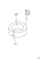
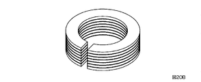
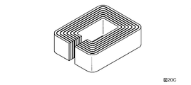
- FIG. 20 is a perspective view showing the shape of the magnetic core provided in the current sensor of the present invention and variations in the stacking direction.
- 20A is an example of a magnetic core laminated in a ring shape and concentric ring
- FIG. 20B is an example of a magnetic core laminated in a ring shape and current conduction direction
- FIG. 20C is a concentric ring having a substantially square C shape. Examples of laminated magnetic cores are shown respectively.
- FIG. 20A is an example of a magnetic core laminated in a ring shape and concentric ring
- FIG. 20B is an example of a magnetic core laminated in a ring shape and current con
- the magnetic core 100 (101 to 108, 200 to 208, 300 to 305) according to the embodiment has been described as having a shape obtained by rounding a plate, but the present invention is not limited to this.
- the shape may be a substantially square C-shape.
- the stacking direction may be any direction other than the circumferential direction. Therefore, as shown in FIG. 20B, the magnetic core may be formed by laminating in the current conduction direction.
- FIG. 20A a flat plate made of a plurality of materials is laminated to form a laminated plate, the laminated plate is formed into a pipe, and then a part of the circumference of the pipe is cut to form a gap. Can be manufactured. This manufacturing process is easy and is one of the preferable manufacturing processes because the gap end surface formed by cutting becomes uniform.
- the magnetic core in FIG. 20A can be manufactured by rounding a laminated plate formed by laminating flat plates made of a plurality of materials into a C shape.
- the magnetic core of FIG. 20C can be manufactured by the same manufacturing method.
- the magnetic core of FIG. 20B In the case of the magnetic core of FIG. 20B, a flat plate made of a plurality of materials is laminated to form a laminated plate, and after punching the laminated plate into a ring shape, a part of the circumference is cut to form a gap. Can be manufactured.
- the magnetic core of FIG. 20B may be formed by alternately laminating a plurality of different ring-shaped sheet materials and then cutting a part of the circumference to form a gap.
Abstract
複数の磁性材料を積層して形成した磁性体コアを用いても、ホール素子の位置バラツキによる感度の変動を抑えることができる電流センサを提供することを目的とする。周の一部にギャップを有し、環状に形成された磁性体コアと、ギャップに配置され、磁性体コアの中空部を通過する被測定電流に応じて変化する磁束を検出する磁電変換素子とを備える。磁性体コアが、複数の磁性材料を周方向以外の方向に積層して形成され、磁電変換素子のセンシング部が存在しうる領域として予め定めた領域(以下、センシング部存在領域という)内における、積層方向の距離がセンシング部の積層方向長さだけ離間した2点の磁束密度が近似するように形成されたことを特徴とする。
Description
本発明は、電流の測定や検出に用いられる磁気比例方式または磁気平衡方式の電流センサに関する。
磁気比例方式の電流検出器に関する先行技術として、例えば特許文献1がある。以下、図21を参照して特許文献1の第5実施形態の電流検出器について説明する。図21は、特許文献1の第5実施形態の電流センサを構成要素に分解して示した斜視図である。
特許文献1の第5実施形態の電流検出器90は樹脂ケース92を備えており、この樹脂ケース92には板状のシートコア94、96が複数枚に重なり合った状態で収容される。これらシートコア94、96は、樹脂ケース92内に収容された状態で1つの磁性体コア98を構成する。図21ではシートコア94、96が2枚ずつ示されているが、実際の枚数はこれよりも多く、それらは図示を省略されている。
シートコア94、96はいずれも略角形のC字形状をなしており、このような形状のシートコア94、96は、板状の磁性材料を打ち抜いて成形されている。その際、各シートコア94、96はその中央位置に開口部94a、96aが形成されるとともに、この開口部94a、96aから一側縁に向けて延びるギャップ用スリット94b、96bが形成される。開口部94a、96aは、シートコア94、96の外形に合わせた略角形である。
樹脂ケース92内にシートコア94、96が重ね合わせた状態で収容されると、それらの開口部94a、96a及びギャップ用スリット94b、96bが重ね合わせ方向でみて相互に合致する。これにより、多数のシートコア94、96から1つの磁性体コア98を構成した状態で、その中央位置に一続きの貫通穴が形成されるとともに、周方向の一部にコアギャップが形成されることになる。
樹脂ケース92内には、収容部92a及びガイドスリーブ92bが形成されている。収容部92aは、図21に示される上方が開放されているが、その下方には底板92cが形成されている。ガイドスリーブ92bは底板92c上から上方に延びており、その内部は中空の電流導通部92dとして形成されている。ガイドスリーブ92bの外形はシートコア94、96の開口部94a、96aより僅かに小さく、また、収容部92aの内側の寸法はシートコア94、96の外形よりも大きい。このためシートコア94、96を樹脂ケース92内に収容する際、各開口部94a、96aがガイドスリーブ92bの外面に沿って案内されることで、シートコア94,96の相互の位置決めが容易に行われるものとなっている。
樹脂ケース92には、シートコア94、96とともにホール素子10もまた収容される。ホール素子10は回路基板12に実装されており、この回路基板12は最外層のシートコア96の上面に重ね合わせられるようにして収容される。このときホール素子10は、各シートコア94、96のギャップ用スリット94b、96b間を通じて挿入されることで、磁性体コア98のコアギャップ内に位置付けられる。
第5実施形態においては、一方のシートコア94が鉄-ニッケル合金(例えばPB=45%パーマロイ、PC=78%パーマロイ)を材料とするものであり、他方のシートコア96が無方向性珪素鋼板を材料とするものである。
この場合、シートコア96は無方向性珪素鋼板であり、電流検出用コアとしての磁気特性に劣る部分(特にヒステリシス巾)があるが、別のシートコア94はパーマロイであり、電流検出用コアとして優れた磁気特性(出力直線性、ヒステリシス巾、飽和特性)を有する。これら異なる磁性材料のシートコア94、96を互いに重ね合わせて磁性体コア98を構成することで、シートコア96に固有の欠点を別のシートコア94により補償することができる。その結果、磁性体コア98全体として良好な磁気特性を発揮することができ、製品として充分な特性を発揮することができる。
また、第5実施形態では、比較的安価な磁性材料である無方向性珪素鋼板と、比較的高価な磁性材料であるパーマロイとを合わせて使用しているため、全体の中に占めるパーマロイの使用量を少なく抑えることができ、それだけ材料費の節減に寄与することができる。
以下、図1を参照して、特許文献1のように複数の材質を積層して形成した磁性体コアを用いる電流検出器の問題点について説明する。図1は、従来技術の複数の材質を積層して形成した磁性体コアを用いる電流検出器の問題点を模式的に示す図である。図1Aは、磁性体コア98のコアギャップにホール素子10が挿入された状態における図21中のA-A断面の模式図である。図1Bは、ホール素子センシング部11の位置バラツキおよび位置バラツキにより生じるホール素子センシング部11を貫く磁束総数のバラツキについて説明する模式図である。図1Aに破線で示すように、ホール素子10内には、磁性体コア98から発生する磁界を検知する領域であるホール素子センシング部11が存在する。ここで、ホール素子センシング部11を含むホール素子10は、回路基板12が収容部92aに収容され、磁性体コア98の最上段のシートコア上に設置されることにより、概略位置決めされる。なお、樹脂ケース92の収容部92a内は図示しないポッティング樹脂により封止される。しかしながら、ホール素子10をこのように概略位置決めしたとしても、図1Bの破線に示すように、ホール素子センシング部11の位置は、製品間で比較して位置バラツキが生じる場合がある。一般に製造工程簡易化のため、磁性体コアとホール素子との高精度な位置決めの構造を有しないことがほとんどである。従って、シートコア94、96が互いに透磁率の異なる材質であれば、被測定電流が等しい場合であっても、センシング部11を貫く磁束の総数が製品間でばらつくこととなり、電流センサの感度に誤差が生じてしまうという問題があった。また、製品間の位置バラツキだけでなく、使用時に電流センサ本体に振動が加わることなどによりセンシング部11の位置が変動して、電流センサの感度が変わってしまう場合もあった。
そこで本発明では、複数の材質を積層して形成した磁性体コアを用いても、ホール素子の位置バラツキによる感度の変動を抑えることができる電流センサを提供することを目的とする。
本発明の電流センサは、周の一部にギャップを有し、環状に形成された磁性体コアと、ギャップに配置され、磁性体コアの中空部を通過する被測定電流に応じて変化する磁束を検出する磁電変換素子とを備える。磁性体コアが、複数の材質を周方向以外の方向に積層して形成され、磁電変換素子のセンシング部が存在しうる領域として予め定めた領域(以下、センシング部存在領域という)内における、積層方向の距離がセンシング部の積層方向長さだけ離間した2点の磁束密度が近似するように形成されたことを特徴とする。
また、上述のセンシング部存在領域の積層方向長さSが、センシング部の積層方向長さLHの2倍よりも小さいものとし、磁性体コアが、センシング部存在領域内の磁束密度の積層方向の分布が長さ(S-LH)/m(ただし、mは1以上の整数)の周期で規則性を有するように形成されていてもよい。
また、上述のセンシング部存在領域の積層方向長さSが、センシング部の積層方向長さLHの2倍以上であるものとし、磁性体コアが、センシング部存在領域内の磁束密度の積層方向の分布が長さLH/m(ただし、mは1以上の整数)の周期で規則性を有するように形成されていてもよい。
また、上述の磁性体コアが、複数の材質を不規則に積層して形成されていてもよい。
また、上述の磁性体コアが、同心環状に積層して形成されていてもよい。
また、上述の磁性体コアが、被測定電流の導通方向に積層して形成されていてもよい。
また、上述の磁性体コアが、複数の異なる材質を積層した平板を環状に丸め、周の一部を切断して形成されていてもよい。
また、上述の磁性体コアが、方向性電磁鋼とアモルファス磁性合金を交互に積層して形成されていてもよい。
また、上述の磁性体コアが、方向性電磁鋼とフェライトを交互に積層して形成されていてもよい。
本発明の電流センサによれば、複数の材質を積層して形成した磁性体コアを用いても、ホール素子の位置バラツキによる感度の変動を抑えることができる。
以下、本発明の実施の形態について、詳細に説明する。なお、同じ機能を有する構成部には同じ番号を付し、重複説明を省略する。
以下、図2、3、4を参照して、本発明の実施例にかかる電流センサの構成について説明する。図2は本発明の実施例に係る電流センサの主要構成要素の分解斜視図である。図3は本発明の実施例に係る電流センサが備える磁性体コアの斜視図である。図4は本発明の実施例に係る電流センサが備えるホールICの三面図であり、図4Aが平面図、図4Bが正面図、図4Cが右側面図である。
本発明の実施例に係る電流センサは、電気自動車又はハイブリッド自動車などの車両において、バッテリとモータなどの機器とを電気的に接続するバスバーまたはケーブル等に流れる電流を検出する装置である。図2に示すように、本発明の実施例に係る電流センサは磁性体コア100(101から108、200から208、300から305、符号は後述する実施例毎に使い分ける)と、ホールIC15と、ホールIC15に接続されたリード線13と、ケース50と、蓋60とを備える。
<磁性体コア>
本発明の磁性体コア100(101から108、200から208、300から305)は、軟磁性材料(保磁力が小さく透磁率が大きい材料、例えば鉄、ケイ素鋼、パーマロイ、センダスト、パーメンジュール、ソフトフェライト、アモルファス磁性合金、ナノクリスタル磁性合金、電磁鋼など)を複数種類積層して形成されている。電磁鋼としては、特定の方向に偏って磁化しないようにした無方向性鋼板、特定の方向のみに磁化しやすくなるようにした方向性鋼板がある。複数の材質の積層方向は、コアの周方向以外の方向であればどんな方向であってもよい。また、材質の種類は2種であってもよいし、3種でもよく、2種以上であれば何種類でもよい。さらに、複数の材質は、不規則に積層されていても構わない。詳細については後述する。
本発明の磁性体コア100(101から108、200から208、300から305)は、軟磁性材料(保磁力が小さく透磁率が大きい材料、例えば鉄、ケイ素鋼、パーマロイ、センダスト、パーメンジュール、ソフトフェライト、アモルファス磁性合金、ナノクリスタル磁性合金、電磁鋼など)を複数種類積層して形成されている。電磁鋼としては、特定の方向に偏って磁化しないようにした無方向性鋼板、特定の方向のみに磁化しやすくなるようにした方向性鋼板がある。複数の材質の積層方向は、コアの周方向以外の方向であればどんな方向であってもよい。また、材質の種類は2種であってもよいし、3種でもよく、2種以上であれば何種類でもよい。さらに、複数の材質は、不規則に積層されていても構わない。詳細については後述する。
<ホールIC(磁電変換素子)>
本発明の電流センサが備えるホールIC15は、磁性体コア100(101から108、200から208、300から305)の中空部30に挿し通されるバスバーまたはケーブル等を流れる被測定電流に応じて変化する磁束を検出して、磁束の検出信号を電気信号として出力する。ホールIC15はリード線13を介して図示しない外部の回路に接続される。本発明ではホールIC15は、ホール素子と電気回路の組み合わせで実現してもよい。ホールIC15、ホール素子は磁電変換素子の一例である。
本発明の電流センサが備えるホールIC15は、磁性体コア100(101から108、200から208、300から305)の中空部30に挿し通されるバスバーまたはケーブル等を流れる被測定電流に応じて変化する磁束を検出して、磁束の検出信号を電気信号として出力する。ホールIC15はリード線13を介して図示しない外部の回路に接続される。本発明ではホールIC15は、ホール素子と電気回路の組み合わせで実現してもよい。ホールIC15、ホール素子は磁電変換素子の一例である。
ケース50は、直方体の箱形状であって上面とひとつの側面が開口している。ケース50の底面55を貫通して円筒状のガイドスリーブ52が設けられており、ガイドスリーブ52の内腔(電流導通部54)には、図示しないバスバーまたはケーブル等を挿し通すことができる。ケース50側面の開口部に近接するガイドスリーブ52の外側面には、外側面に垂直な板状の凸部であるストッパ53が形成されている。ケース50内壁とガイドスリーブ52の外側面に囲まれた領域を収容部51と呼ぶ。図3に示すように、磁性体コア100(101から108、200から208、300から305)は、その周の一部にギャップ20を有し、環状に形成されている。磁性体コア100(101から108、200から208、300から305)は板状の材質を中空部30を囲んで長手方向に環状に丸めて形成され、その長手方向の両端がギャップ20を介して対向している。
ガイドスリーブ52の外形は磁性体コア100(101から108、200から208、300から305)の中空部30より僅かに小さい。またストッパ53のガイドスリーブ52周方向の幅は、ギャップ20のコア周方向の幅より僅かに小さい。また、収容部51の内側の寸法は磁性体コア100(101から108、200から208、300から305)の外形よりも大きい。このため磁性体コア100(101から108、200から208、300から305)をケース50内に収容する際、中空部30、およびギャップ20がガイドスリーブ52、およびストッパ53の外面に沿って案内され、底面55に載せられることで、磁性体コア100(101から108、200から208、300から305)の概略位置決めが行われる。
蓋60の外面の略中心に鉛直下方向に長い長円凹部61が設けられており、長円凹部61内には、鉛直方向一列に図示しないリード線用穴が5つ設けられている。一方、図4に示すように、ホールIC15は、直方体形状のケース15bとケース15b内の図示しない磁電変換用回路基板、ホールICセンシング部11(破線で概略位置を図示)から構成される。ホールIC15の下端にはリード線13(13a、13b、13c、13d、13e)が5本設けられ、リード線13は、蓋60の長円凹部61に設けられたリード線用穴に通される。このとき、5本のリード線13のうち、中心のリード線13cには、リード線13cの一部分を鍔状に太くした鍔部13c-1が設けられており、鍔部13c-1が上述のリード線穴に閊(つか)えることで、ホールIC15を蓋60に対して保持する。蓋60は、ケース50の側面開口部に取り付けられる。このとき、ホールIC15のリード線13を設けた端部と反対側の端部15aは、ストッパ53に接触して概略位置決めされる。
以下、図5、図6を参照して磁性体コア100(101から108、200から208、300から305)と、ホールICセンシング部11の位置関係について説明する。図5は本発明の実施例に係る電流センサが備える磁性体コアとホールICセンシング部の位置関係を模式的に示す図(平面図)である。図6は本発明の実施例に係る電流センサが備える磁性体コアとホールICセンシング部の位置関係を模式的に示す図(正面図)である。図5に示すように、ホールICセンシング部11のコア外縁方向の端部を外縁方向端部11aと呼ぶこととし、ホールICセンシング部11のコア中心方向の端部を中心方向端部11bと呼ぶこととする。また、図6に示すように、ホールICセンシング部11のコア上面方向の端部を上方向端部11cと呼ぶこととし、ホールICセンシング部11のコア下面方向の端部を下方向端部11dと呼ぶこととする。
次に、図7を参照して、ホールICセンシング部11の位置バラツキについて説明する。図7に示すようにホールICセンシング部11はコア外縁-中心方向に対しても、コア上面-下面方向に対しても製品間、または使用時の振動の付加によって位置バラツキが生じる可能性がある。これは特許文献1の場合と同様である。本発明では、ホールICセンシング部11の位置バラツキとして最大に見積もった領域をセンシング部存在領域としてあらかじめ定義しておく。センシング部存在領域は、ケース50と磁性体コア100(101から108、200から208、300から305)の間に生じるガタの設計値、蓋60とケース50との間に生じるガタの設計値、蓋60とホールIC15との間で生じるガタの設計値から、理論的に生じうる最大のガタを計算することにより見積もってもよい。また、実際に組み立てられた製品を抜き取り検査して、組み立てられた状態のホールIC15の位置を実測して、見積もってもよい。センシング部存在領域は、ホールICセンシング部11が確実に存在する領域として、余裕を持って設定しておけばよい。センシング部存在領域の積層方向長さをSと表して、後述する磁性体コアの磁束密度分布決定の際のパラメータとして用いる。ここで、上述したように、本発明の磁性体コアの積層方向はコアの周方向以外の方向であればどんな方向でもよい。例えば、磁性体コアを同心環上に形成した場合には、積層方向はコア外縁-中心方向となる。従って、この場合センシング部存在領域の積層方向長さSとは、ホールICセンシング部11の外縁方向端部11aの外縁方向の最大ずれ位置、ホールICセンシング部11の中心方向端部11bの中心方向の最大ずれ位置に基づいて決められることになる。また、例えば、磁性体コアを被測定電流の導通方向に積層して形成した場合には、積層方向はコア上面-下面方向となる。従って、この場合センシング部存在領域の積層方向長さSとは、ホールICセンシング部11の上方向端部11cの上方向の最大ずれ位置、ホールICセンシング部11の下方向端部11dの下方向の最大ずれ位置に基づいて決められることになる。
センシング部存在領域について、図8、図9を用いてさらに詳細に検討する。ここで、ホールICセンシング部11の積層方向長さをLHと表し、以下、S<2LHの場合を実施例1として説明し、以下、S≧2LHの場合を実施例2として説明を進める。図8は実施例1の電流センサのギャップにおける磁束密度分布の特徴を模式的に示す図である。図9は実施例2の電流センサのギャップにおける磁束密度分布の特徴を模式的に示す図である。
図8に示すとおり、積層方向がコア外縁-中心方向である場合、外縁方向端部11aの外縁方向最大ずれ位置の積層方向の座標をEEと呼ぶ。同様に、外縁方向端部11aの中心方向最大ずれ位置の積層方向の座標をECと呼ぶ。同様に、中心方向端部11bの外縁方向最大ずれ位置の積層方向の座標をCEと呼ぶ。同様に、中心方向端部11bの中心方向最大ずれ位置の積層方向の座標をCCと呼ぶ。
一方、積層方向がコア上面-下面方向である場合、上方向端部11cの上方向最大ずれ位置の積層方向の座標をEEと呼ぶ。同様に、上方向端部11cの下方向最大ずれ位置の積層方向の座標をECと呼ぶ。同様に、下方向端部11dの上方向最大ずれ位置の積層方向の座標をCEと呼ぶ。同様に、下方向端部11dの下方向最大ずれ位置の積層方向の座標をCCと呼ぶ。座標EE、EC、CE、CCは図9においても同じ定義で用いられる。
図8の場合、S<2LHが前提条件となっているため、積層方向がいずれであったとしても、座標の並びは、向かって左からEE、EC、CE、CCの順になる。ここで、ホールICセンシング部11の左端が座標EEにある状態からスタートして、徐々にホールICセンシング部11を図中右方向に移動させ、ホールICセンシング部11の右端を座標CCに到達させることを考える。このとき、ホールICセンシング部11が右に移動するにつれて、座標EE右近傍で発生している磁束が、ホールICセンシング部11を通過しなくなることがわかる。その代わりに、座標CE右近傍で発生している磁束が、ホールICセンシング部11を新たに貫くようになる。従って、ホールICセンシング部11を貫く磁束の総数を一定に保ちたい場合には、ホールICセンシング部11の移動によってホールICセンシング部11に影響を及ぼさなくなる座標における磁束密度と、当該移動によって新たにホールICセンシング部11に影響を与える座標における磁束密度とが近似していればよいことになる。具体的には、座標EE近傍と座標CE近傍の磁束密度が近似していればよい。同様に、座標EC近傍と座標CC近傍の磁束密度が近似していればよい。これらの対応する座標はいずれも距離LH離間している。なお、座標ECと座標CEの間については、磁束密度に何らの条件も課されない。S<2LHの条件では、この領域は、ホールICセンシング部11がセンシング部存在領域内のどんな位置にあったとしても常にホールICセンシング部11を貫通する磁束を発生しているため、ホールICセンシング部11を貫く磁束の総数に影響を与えないからである。
また、ホールICセンシング部11に影響を与えない、図中のコア左端部から座標EEの区間、座標CCから図中のコア右端部の区間についてはホールICセンシング部11を貫く磁束の総数に影響を与えないため、何らの条件も課されない。
図8において説明した実施例1の電流センサの磁性体コア100から108が満たすべき条件を再度まとめておく。実施例1の電流センサの磁性体コア100から108は、センシング部存在領域内における積層方向の距離がLHだけ離間した2点の磁束密度が近似するように形成されることを条件とする。S<2LHの条件では、座標ECから座標CEの区間における各座標において、対応する距離がLH離間する点がセンシング部存在領域の外にしか存在しないため、何らの条件も課されない。
一方、図9の場合、S≧2LHが前提条件となっているため、積層方向がいずれであったとしても、座標の並びは、向かって左からEE、CE、EC、CCの順になる。ここで、ホールICセンシング部11の左端が座標EEにある状態からスタートして、徐々にホールICセンシング部11を図中右方向に移動させ、ホールICセンシング部11の右端を座標CCに到達させることを考える。このとき、ホールICセンシング部11が右に移動するにつれて、座標EE近傍で発生している磁束が、ホールICセンシング部11を通過しなくなることがわかる。その代わりに、座標CE近傍で発生している磁束が、ホールICセンシング部11を新たに貫くようになる。従って、ホールICセンシング部11を貫く磁束の総数を一定に保ちたい場合には、ホールICセンシング部11の移動によってホールICセンシング部11に影響を及ぼさなくなる座標における磁束密度と、当該移動によって新たにホールICセンシング部11に影響を与える座標における磁束密度とが近似していればよいことになる。具体的には、座標EE近傍と座標CE近傍の磁束密度が近似していればよい。これらの対応する座標はいずれも距離LH離間している。ここまでは、図8と同様である。しかしながら、図9の場合は、図8に存在した座標ECからCE間の条件が課されない領域が存在しない。
また、ホールICセンシング部11に影響を与えない、図中のコア左端部から座標EEの区間、座標CCから図中のコア右端部の区間についてはホールICセンシング部11を貫く磁束の総数に影響を与えないため、何らの条件も課されない。これは図8の場合と同じである。
図9において説明した実施例2の電流センサの磁性体コア200から208が満たすべき条件を再度まとめておく。実施例2の電流センサの磁性体コア200から208は、センシング部存在領域内における積層方向の距離がLHだけ離間した2点の磁束密度が近似するように形成されることを条件とする。
図8、図9で説明した本発明の上位概念は、LH離間した領域内の任意の2点の磁束密度が近似していることのみを規定しているので、例えば、図8における座標EEからCC区間における磁束密度分布が不規則な分布であっても構わない。同様に、図9において座標EEからCE区間における磁束密度分布が不規則な分布であっても構わない。
以下、本発明の実施例1、2の磁性体コアから発生する磁束密度分布が満たすべき条件について、図10、図11を参照してさらに詳細に検討する。図10は実施例1の電流センサが備える磁性体コアの磁束密度分布の規則性を模式的に示す模式図である。図11は実施例2の電流センサが備える磁性体コアの磁束密度分布の規則性を模式的に示す図である。
前述したように、本発明の上位概念では、LH離間した存在領域内の任意の2点の磁束密度が近似することにより相互に補償し合う関係にあれば、電流センサの感度の変動を抑えることができる。換言すれば、実施例1のS<2LHの条件では、座標EEと座標ECの積層方向距離がS-LHであるから、少なくとも座標EEからEC間に波長λB=S-LHの周期的分布が存在し、座標CEからCC間にも同様に、波長λB=S-LHの周期的分布が存在すれば補償関係が成立することになる。さらに、磁束密度分布の波長λBについては、図10に示すように、磁束密度分布が(S-LH)/m(ただし、mは1以上の整数)の周期で規則性を有するようにしても補償関係が成立する。図10の中段のグラフにおいてはm=4として図示してある。
一方、実施例2のS≧2LHの条件では、座標EEと座標CEの積層方向距離がLHであるから、少なくとも座標EEからCE間に波長λB=LHの周期的分布が存在し、続く長さLHの各区間においても波長λB=LHの周期的分布が存在し、座標ECからCC間にも同様に、波長λB=LHの周期的分布が存在すれば補償関係が成立することになる。さらに、磁束密度分布の波長λBについては、図11に示すように、磁束密度分布がLH/m(ただし、mは1以上の整数)の周期で規則性を有するようにしても補償関係が成立する。図11の中段のグラフにおいてはm=3として図示してある。
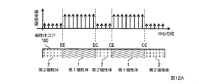
以下、図12を参照して、実施例1の電流センサの磁性体コアに採用可能な応用例1から応用例3について説明する。図12は実施例1の電流センサに採用可能な応用例を示す模式図である。図12Aは応用例1の磁性体コア100の構成を示す模式図、図12Bは応用例2の磁性体コア101の構成を示す模式図、図12Cは応用例3の磁性体コア102の構成を示す模式図である。
[応用例1]
上述したように、LH離間した存在領域内の任意の2点の磁束密度が近似していることが条件となり、座標ECからCE間における磁束密度には何らの条件も課されないのであるから、例えば、座標EEからEC間については、磁束密度がフラットな分布となるように、一種類の磁性体(第1磁性体1とする)のみで構成することとし、座標EEからEC間の各座標点からLH離間した点が存在する座標CEからCC間についても同じ第1磁性体1のみで構成して、座標CEからCC間がフラットな磁束密度分布とすればよい。磁性体コア100の図中のコア左端部から座標EEの区間、座標CCから図中のコア右端部の区間、座標ECからCE間の区間については何らの条件も課されないため、例えば第1磁性体1とは異なる第2磁性体2の層を形成すればよい。
上述したように、LH離間した存在領域内の任意の2点の磁束密度が近似していることが条件となり、座標ECからCE間における磁束密度には何らの条件も課されないのであるから、例えば、座標EEからEC間については、磁束密度がフラットな分布となるように、一種類の磁性体(第1磁性体1とする)のみで構成することとし、座標EEからEC間の各座標点からLH離間した点が存在する座標CEからCC間についても同じ第1磁性体1のみで構成して、座標CEからCC間がフラットな磁束密度分布とすればよい。磁性体コア100の図中のコア左端部から座標EEの区間、座標CCから図中のコア右端部の区間、座標ECからCE間の区間については何らの条件も課されないため、例えば第1磁性体1とは異なる第2磁性体2の層を形成すればよい。
[応用例2]
磁性体コア100を変形した応用例として、本応用例の磁性体コア101のように、座標ECからCE間の区間について第1磁性体1とも第2磁性体2とも異なる材質(第4磁性体4とする)で構成してもよい。この場合3種類の磁性体で磁性体コアが形成されたことになる。
磁性体コア100を変形した応用例として、本応用例の磁性体コア101のように、座標ECからCE間の区間について第1磁性体1とも第2磁性体2とも異なる材質(第4磁性体4とする)で構成してもよい。この場合3種類の磁性体で磁性体コアが形成されたことになる。
[応用例3]
磁性体コア100を変形した応用例として、本応用例の磁性体コア102のように、図中のコア左端部から座標EEの区間、座標CCから図中のコア右端部の区間、座標ECからCE間の区間を磁性体でない物質(非磁性体9とする)で構成してもよい。このように、非磁性体が含まれる場合でも、磁束の補償関係が成り立つ限り、ホールICセンシング部11の位置ずれによる電流センサの感度の変動を抑制することができる。これ以外にも、図中のコア左端部から座標EEの区間、座標CCから図中のコア右端部の区間、座標ECからCE間の区間については、複数種類の磁性体を積層して構成してもよい。
磁性体コア100を変形した応用例として、本応用例の磁性体コア102のように、図中のコア左端部から座標EEの区間、座標CCから図中のコア右端部の区間、座標ECからCE間の区間を磁性体でない物質(非磁性体9とする)で構成してもよい。このように、非磁性体が含まれる場合でも、磁束の補償関係が成り立つ限り、ホールICセンシング部11の位置ずれによる電流センサの感度の変動を抑制することができる。これ以外にも、図中のコア左端部から座標EEの区間、座標CCから図中のコア右端部の区間、座標ECからCE間の区間については、複数種類の磁性体を積層して構成してもよい。
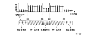
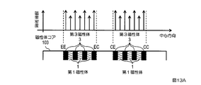
以下、図13を参照して、実施例1の電流センサの磁性体コアに採用可能な応用例4から応用例6について説明する。図13は実施例1の電流センサに採用可能な応用例を示す模式図である。図13Aは応用例4の磁性体コア103の構成を示す模式図、図13Bは応用例5の磁性体コア104の構成を示す模式図、図13Cは応用例6の磁性体コア105の構成を示す模式図である。
[応用例4]
上述したように、LH離間した存在領域内の任意の2点の磁束密度が近似していることが条件となり、座標ECからCE間における磁束密度には何らの条件も課されない。従って、例えば、EEからEC間において二種類の磁性体を任意のパターンに配置し、CEからCC間において、EEからEC間に用いられた二種類の磁性体を、EEからEC間における配置と同じパターンに配置して磁性体を形成しても良い。図13Aに示すように、本応用例の磁性体コア103は、座標EEからEC、CEからCCの区間において、第1磁性体1と第3磁性体3が交互に配置されて、同一の磁束密度分布を形成している。なお、本応用例、および以下の応用例5から9においては、図中のコア左端部から座標EEの区間、座標CCから図中のコア右端部の区間、座標ECからCE間の区間についての言及を省略するが、この区間については、応用例1から3同様、磁性体、非磁性体、複数種類の磁性体を積層して形成するなど任意の構成で構わない。
上述したように、LH離間した存在領域内の任意の2点の磁束密度が近似していることが条件となり、座標ECからCE間における磁束密度には何らの条件も課されない。従って、例えば、EEからEC間において二種類の磁性体を任意のパターンに配置し、CEからCC間において、EEからEC間に用いられた二種類の磁性体を、EEからEC間における配置と同じパターンに配置して磁性体を形成しても良い。図13Aに示すように、本応用例の磁性体コア103は、座標EEからEC、CEからCCの区間において、第1磁性体1と第3磁性体3が交互に配置されて、同一の磁束密度分布を形成している。なお、本応用例、および以下の応用例5から9においては、図中のコア左端部から座標EEの区間、座標CCから図中のコア右端部の区間、座標ECからCE間の区間についての言及を省略するが、この区間については、応用例1から3同様、磁性体、非磁性体、複数種類の磁性体を積層して形成するなど任意の構成で構わない。
[応用例5]
本応用例の磁性体コア104は、座標EEからEC、CEからCCの区間において、第1磁性体1と第3磁性体3が交互に配置されて、同一の磁束密度分布を形成されている点で応用例4と同じであるが、第1磁性体1と第3磁性体3の層の厚みを異ならせてある。具体的には第3磁性体3を第1磁性体1の層よりも薄く形成した。
本応用例の磁性体コア104は、座標EEからEC、CEからCCの区間において、第1磁性体1と第3磁性体3が交互に配置されて、同一の磁束密度分布を形成されている点で応用例4と同じであるが、第1磁性体1と第3磁性体3の層の厚みを異ならせてある。具体的には第3磁性体3を第1磁性体1の層よりも薄く形成した。
[応用例6]
本応用例の磁性体コア105は、応用例4、5と同じように、座標EEからEC、CEからCCの区間において、2種類の材質を交互に配置して形成されている。本応用例の磁性体コア105は、磁性体(図中、第3磁性体3と表記したが、磁性体の種類に特に制限はない)と、非磁性体9とを交互に積層して形成されている。このように、座標EEからEC、CEからCCの区間において、磁性体と非磁性体とを用いて、任意のパターンで積層することによっても磁性体コアを形成することができる。
本応用例の磁性体コア105は、応用例4、5と同じように、座標EEからEC、CEからCCの区間において、2種類の材質を交互に配置して形成されている。本応用例の磁性体コア105は、磁性体(図中、第3磁性体3と表記したが、磁性体の種類に特に制限はない)と、非磁性体9とを交互に積層して形成されている。このように、座標EEからEC、CEからCCの区間において、磁性体と非磁性体とを用いて、任意のパターンで積層することによっても磁性体コアを形成することができる。
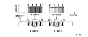
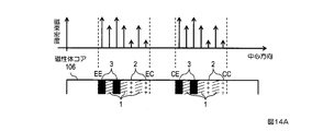
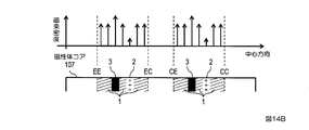
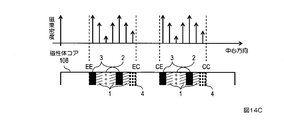
以下、図14を参照して、実施例1の電流センサの磁性体コアに採用可能な応用例7から応用例9について説明する。図14は実施例1の電流センサに採用可能な応用例を示す模式図である。図14Aは応用例7の磁性体コア106の構成を示す模式図、図14Bは応用例8の磁性体コア107の構成を示す模式図、図14Cは応用例9の磁性体コア108の構成を示す模式図である。
[応用例7]
上述したように、LH離間した存在領域内の任意の2点の磁束密度が近似していることが条件となり、座標ECからCE間における磁束密度には何らの条件も課されない。従って、例えば、EEからEC間において三種類の磁性体を任意のパターンに配置し、CEからCC間において、EEからEC間に用いられた三種類の磁性体を、EEからEC間における配置と同じパターンに配置して磁性体を形成しても良い。図14Aに示すように、本応用例の磁性体コア106は、座標EEからEC、CEからCCの区間において、第1磁性体1と第2磁性体2と第3磁性体3とが同一のパターンに配置されて、同一の磁束密度分布を形成している。
上述したように、LH離間した存在領域内の任意の2点の磁束密度が近似していることが条件となり、座標ECからCE間における磁束密度には何らの条件も課されない。従って、例えば、EEからEC間において三種類の磁性体を任意のパターンに配置し、CEからCC間において、EEからEC間に用いられた三種類の磁性体を、EEからEC間における配置と同じパターンに配置して磁性体を形成しても良い。図14Aに示すように、本応用例の磁性体コア106は、座標EEからEC、CEからCCの区間において、第1磁性体1と第2磁性体2と第3磁性体3とが同一のパターンに配置されて、同一の磁束密度分布を形成している。
[応用例8]
応用例7と同様に、本応用例の磁性体コア107は、座標EEからEC、CEからCCの区間において、第1磁性体1と第2磁性体2と第3磁性体3が配置されて、同一の磁束密度分布を形成している。本応用例では、第1磁性体1を他の層よりも厚く形成している。
応用例7と同様に、本応用例の磁性体コア107は、座標EEからEC、CEからCCの区間において、第1磁性体1と第2磁性体2と第3磁性体3が配置されて、同一の磁束密度分布を形成している。本応用例では、第1磁性体1を他の層よりも厚く形成している。
[応用例9]
本応用例の磁性体コア108は、座標EEからEC、CEからCCの区間において、4種の磁性体(第1磁性体1、第2磁性体2、第3磁性体3、第4磁性体4)を配置して形成されて、同一の磁束密度分布を形成している。このように、応用例7から応用例9では、複数種類の磁性体を不規則に配置して形成された磁性体コアを示したが、これらを規則的に配置して磁性体コアを形成することも可能であることはいうまでもない。この場合、図10で説明したようにS<2LHの条件では、磁束密度分布の波長λB=(S-LH)/m(ただし、mは1以上の整数)の周期で規則性を有するようにしても補償関係が成立する。
本応用例の磁性体コア108は、座標EEからEC、CEからCCの区間において、4種の磁性体(第1磁性体1、第2磁性体2、第3磁性体3、第4磁性体4)を配置して形成されて、同一の磁束密度分布を形成している。このように、応用例7から応用例9では、複数種類の磁性体を不規則に配置して形成された磁性体コアを示したが、これらを規則的に配置して磁性体コアを形成することも可能であることはいうまでもない。この場合、図10で説明したようにS<2LHの条件では、磁束密度分布の波長λB=(S-LH)/m(ただし、mは1以上の整数)の周期で規則性を有するようにしても補償関係が成立する。
このように、本発明の実施例1の電流センサの磁性体コア100から108によれば、ギャップ20にホールIC15を配置する場合の位置バラツキによる電流センサ感度の変動が抑制されるため、電流センサの製品間(動作間)バラツキを抑え、より高精度な電流センサを実現することができる。
また、本発明の実施例1の電流センサの磁性体コア100から108のように、複数の材質による積層構造を採用することにより、それぞれの材質がもつデメリットを補い、それぞれの物質がもつメリットを享受することができる。例えば電磁鋼板は、渦電流損等の鉄損により、10kHz以上の高周波電流の測定が出来ないというデメリットを有するが、電磁鋼板と周波数特性の良い材料とを組み合わせて磁性体コアを形成することで周波数特性が改善された電流センサを実現できる。また、例えばフェライトは、飽和磁束密度が小さく大電流領域においてセンサ感度が低下してしまうというデメリットを有するが、フェライトと飽和磁束密度の高い方向性電磁鋼板とを積層して磁性体コアを形成することで大電流領域の感度を改善した電流センサを実現できる。また、アモルファス磁性合金は軟磁性材料としての特性は良好だが、機械的強度が弱いというデメリットを有するが、アモルファス磁性合金と機械的強度の高い方向性電磁鋼板とを積層して磁性体コアを形成することで、機械的強度の高い磁性体コア並びに電流センサを実現できる。
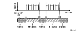
以下、図15を参照して、実施例2の電流センサの磁性体コアに採用可能な応用例10から応用例12について説明する。図15は実施例2の電流センサに採用可能な応用例を示す模式図である。図15Aは応用例10の磁性体コア200の構成を示す模式図、図15Bは応用例11の磁性体コア201の構成を示す模式図、図15Cは応用例12の磁性体コア202の構成を示す模式図である。
[応用例10]
上述したように、LH離間した存在領域内の任意の2点の磁束密度が近似していることが条件となるから、例えば、座標EEからCC間については、磁束密度がフラットな分布となるように、一種類の磁性体(第1磁性体1)のみで構成すればよい。磁性体コア200の図中のコア左端部から座標EEの区間、座標CCから図中のコア右端部の区間については何らの条件も課されないため、例えば第1磁性体1とは異なる第2磁性体2の層を形成すればよい。
上述したように、LH離間した存在領域内の任意の2点の磁束密度が近似していることが条件となるから、例えば、座標EEからCC間については、磁束密度がフラットな分布となるように、一種類の磁性体(第1磁性体1)のみで構成すればよい。磁性体コア200の図中のコア左端部から座標EEの区間、座標CCから図中のコア右端部の区間については何らの条件も課されないため、例えば第1磁性体1とは異なる第2磁性体2の層を形成すればよい。
[応用例11]
磁性体コア200を変形した応用例として、本応用例の磁性体コア201のように、座標CCから図中のコア右端部の区間について第1磁性体1とも第2磁性体2とも異なる材質(第4磁性体4とする)で構成してもよい。この場合3種類の磁性体で磁性体コアが形成されたことになる。
磁性体コア200を変形した応用例として、本応用例の磁性体コア201のように、座標CCから図中のコア右端部の区間について第1磁性体1とも第2磁性体2とも異なる材質(第4磁性体4とする)で構成してもよい。この場合3種類の磁性体で磁性体コアが形成されたことになる。
[応用例12]
磁性体コア200を変形した応用例として、本応用例の磁性体コア202のように、図中のコア左端部から座標EEの区間、座標CCから図中のコア右端部の区間を磁性体でない物質(非磁性体9)で構成してもよい。このように、非磁性体が含まれる場合でも、磁束の補償関係が成り立つ限り、ホールICセンシング部11の位置ずれによる電流センサの感度の変動を抑制することができる。これ以外にも、図中のコア左端部から座標EEの区間、座標CCから図中のコア右端部の区間については、複数種類の磁性体を積層して構成してもよい。
磁性体コア200を変形した応用例として、本応用例の磁性体コア202のように、図中のコア左端部から座標EEの区間、座標CCから図中のコア右端部の区間を磁性体でない物質(非磁性体9)で構成してもよい。このように、非磁性体が含まれる場合でも、磁束の補償関係が成り立つ限り、ホールICセンシング部11の位置ずれによる電流センサの感度の変動を抑制することができる。これ以外にも、図中のコア左端部から座標EEの区間、座標CCから図中のコア右端部の区間については、複数種類の磁性体を積層して構成してもよい。
以下、図16を参照して、実施例2の電流センサの磁性体コアに採用可能な応用例13から応用例15について説明する。図16は実施例2の電流センサに採用可能な応用例を示す模式図である。図16Aは応用例13の磁性体コア203の構成を示す模式図、図16Bは応用例14の磁性体コア204の構成を示す模式図、図16Cは応用例15の磁性体コア205の構成を示す模式図である。
[応用例13]
上述したように、LH離間した存在領域内の任意の2点の磁束密度が近似していることが条件となる。従って、図11で説明したようにS≧2LHの条件では、磁束密度分布の波長λB=LH/m(ただし、mは1以上の整数)の周期で規則性を有するようにしても補償関係が成立する。図16Aに示すように、本応用例の磁性体コア203は、座標EEからCCの区間において、第1磁性体1と第3磁性体3が交互に配置されて、波長λB=LH/3となるように形成されている。なお、本応用例、および以下の応用例14から18においては、図中のコア左端部から座標EEの区間、座標CCから図中のコア右端部の区間についての言及を省略するが、この区間については、応用例1から3や応用例10から12同様、磁性体、非磁性体、複数種類の磁性体を積層して形成するなど任意の構成で構わない。
上述したように、LH離間した存在領域内の任意の2点の磁束密度が近似していることが条件となる。従って、図11で説明したようにS≧2LHの条件では、磁束密度分布の波長λB=LH/m(ただし、mは1以上の整数)の周期で規則性を有するようにしても補償関係が成立する。図16Aに示すように、本応用例の磁性体コア203は、座標EEからCCの区間において、第1磁性体1と第3磁性体3が交互に配置されて、波長λB=LH/3となるように形成されている。なお、本応用例、および以下の応用例14から18においては、図中のコア左端部から座標EEの区間、座標CCから図中のコア右端部の区間についての言及を省略するが、この区間については、応用例1から3や応用例10から12同様、磁性体、非磁性体、複数種類の磁性体を積層して形成するなど任意の構成で構わない。
[応用例14]
本応用例の磁性体コア204は、座標EEからCCの区間において、第1磁性体1と第3磁性体3が交互に配置されて、波長λB=LH/3となるように形成されている点で応用例13と同じであるが、第1磁性体1と第3磁性体3の層の厚みを異ならせてある。具体的には第3磁性体3を第1磁性体1の層よりも薄く形成した。
本応用例の磁性体コア204は、座標EEからCCの区間において、第1磁性体1と第3磁性体3が交互に配置されて、波長λB=LH/3となるように形成されている点で応用例13と同じであるが、第1磁性体1と第3磁性体3の層の厚みを異ならせてある。具体的には第3磁性体3を第1磁性体1の層よりも薄く形成した。
[応用例15]
本応用例の磁性体コア205は、応用例13、14と同じように、座標EEからCCの区間において、2種類の材質が交互に配置されて、波長λB=LH/3となるように形成されている。本応用例の磁性体コア205は、磁性体(図中、第3磁性体3と表記したが、磁性体の種類に特に制限はない)と、非磁性体9とを交互に積層して形成されている。このように、座標EEからCCの区間において、磁性体と非磁性体とを用いて、波長λB=LH/mで積層することによっても磁性体コアを形成することができる。
本応用例の磁性体コア205は、応用例13、14と同じように、座標EEからCCの区間において、2種類の材質が交互に配置されて、波長λB=LH/3となるように形成されている。本応用例の磁性体コア205は、磁性体(図中、第3磁性体3と表記したが、磁性体の種類に特に制限はない)と、非磁性体9とを交互に積層して形成されている。このように、座標EEからCCの区間において、磁性体と非磁性体とを用いて、波長λB=LH/mで積層することによっても磁性体コアを形成することができる。
以下、図17を参照して、実施例2の電流センサの磁性体コアに採用可能な応用例16から応用例18について説明する。図17は実施例2の電流センサに採用可能な応用例を示す模式図である。図17Aは応用例16の磁性体コア206の構成を示す模式図、図17Bは応用例17の磁性体コア207の構成を示す模式図、図17Cは応用例18の磁性体コア208の構成を示す模式図である。
[応用例16]
上述したように、LH離間した存在領域内の任意の2点の磁束密度が近似していることが条件となる。従って、図11で説明したようにS≧2LHの条件では、磁束密度分布の波長λB=LHの周期で規則性を有するようにしても補償関係が成立する。図17Aに示すように、本応用例の磁性体コア206は、座標EEからCCの区間において、第1磁性体1と第2磁性体2と第3磁性体3とを配置して、波長λB=LHとなるようなパターンを形成し、これを繰り返し積層して形成されている。
上述したように、LH離間した存在領域内の任意の2点の磁束密度が近似していることが条件となる。従って、図11で説明したようにS≧2LHの条件では、磁束密度分布の波長λB=LHの周期で規則性を有するようにしても補償関係が成立する。図17Aに示すように、本応用例の磁性体コア206は、座標EEからCCの区間において、第1磁性体1と第2磁性体2と第3磁性体3とを配置して、波長λB=LHとなるようなパターンを形成し、これを繰り返し積層して形成されている。
[応用例17]
応用例16と同様に、本応用例の磁性体コア207は、座標EEからCCの区間において、第1磁性体1と第2磁性体2と第3磁性体3を配置して、波長λB=LHとなるようなパターンを形成し、これを繰り返し積層して形成されている。本応用例では、第1磁性体1を他の層よりも厚く形成している。
応用例16と同様に、本応用例の磁性体コア207は、座標EEからCCの区間において、第1磁性体1と第2磁性体2と第3磁性体3を配置して、波長λB=LHとなるようなパターンを形成し、これを繰り返し積層して形成されている。本応用例では、第1磁性体1を他の層よりも厚く形成している。
[応用例18]
本応用例の磁性体コア208は、座標EEからCCの区間において、4種の磁性体(第1磁性体1、第2磁性体2、第3磁性体3、第4磁性体4)を配置して、波長λB=LHとなるようなパターンを形成し、これを繰り返し積層して形成されている。
本応用例の磁性体コア208は、座標EEからCCの区間において、4種の磁性体(第1磁性体1、第2磁性体2、第3磁性体3、第4磁性体4)を配置して、波長λB=LHとなるようなパターンを形成し、これを繰り返し積層して形成されている。
このように、本実施例の電流センサの磁性体コア200から208によれば、実施例1と同様に、電流センサの製品間(動作間)バラツキを抑え、より高精度な電流センサを実現することができ、それぞれの材質がもつデメリットを補い、それぞれの物質がもつメリットを享受することができる。
以下、図18を参照して、実施例2を変形した実施例3の電流センサの磁性体コアに採用可能な応用例19から応用例24について説明する。図18は実施例3の電流センサに採用可能な応用例を示す模式図である。図18Aから図18Fはそれぞれ応用例19から24の磁性体コア300から305の構成を示す模式図である。
図18に示すように、実施例2で設定していたセンシング部存在領域である座標EEからCCの区間を、磁性体コア全体が含まれる領域に拡張することも可能である。このようにすることで、センシング部存在領域が不明であったとしても、S≧2LHの条件の下、磁性体コア全体を磁束密度分布の波長λB=LH/m(ただし、mは1以上の整数)の周期で規則性を有するように形成すれば、図11で述べたように補償関係が成立する。従って、本実施例では、図中コア左端部からコア右端部の領域を座標EEからCCと設定し、実施例2の応用例13から18を変形して応用例19から応用例24とした。
このように、本実施例の電流センサの磁性体コア300から305によれば、実施例1、2と同じ効果に加え、センシング部存在領域が不明であったとしても、S≧2LHの条件の下、補償関係が成立するため、電流センサの製品間(動作間)バラツキを抑えることができる。
<磁性体>
実施例1から3において第1磁性体1から第4磁性体4として磁性体の種類を複数示したが、これらの磁性体は具体的には、上述した軟磁性材料である例えば鉄、ケイ素鋼、パーマロイ、センダスト、パーメンジュール、ソフトフェライト(フェライトシート)、アモルファス磁性合金(アモルファスリボン)、ナノクリスタル磁性合金、電磁鋼(無方向性鋼板、方向性鋼板)などのいずれであってもよい。磁性体を2種類として構成する場合に好適な組み合わせは、電磁鋼板と周波数特性の良い材料、フェライトと方向性電磁鋼板、アモルファス磁性合金と方向性電磁鋼板、アモルファス磁性合金とフェライトなどである。
実施例1から3において第1磁性体1から第4磁性体4として磁性体の種類を複数示したが、これらの磁性体は具体的には、上述した軟磁性材料である例えば鉄、ケイ素鋼、パーマロイ、センダスト、パーメンジュール、ソフトフェライト(フェライトシート)、アモルファス磁性合金(アモルファスリボン)、ナノクリスタル磁性合金、電磁鋼(無方向性鋼板、方向性鋼板)などのいずれであってもよい。磁性体を2種類として構成する場合に好適な組み合わせは、電磁鋼板と周波数特性の良い材料、フェライトと方向性電磁鋼板、アモルファス磁性合金と方向性電磁鋼板、アモルファス磁性合金とフェライトなどである。
<非磁性体>
実施例1から3において非磁性体9として示したが、非磁性体とは具体的には、反磁性体や常磁性体を意味する。
実施例1から3において非磁性体9として示したが、非磁性体とは具体的には、反磁性体や常磁性体を意味する。
<λB≠LH/m(LH≠λB×m)の場合>
以下、図19を参照して、波長λB=LH/m(LH=λB×m)とならない場合について検討する。図19はセンシング部積層方向長さLHが波長λBの整数倍にならない場合の磁束総数の変化について模式的に示す図である。
以下、図19を参照して、波長λB=LH/m(LH=λB×m)とならない場合について検討する。図19はセンシング部積層方向長さLHが波長λBの整数倍にならない場合の磁束総数の変化について模式的に示す図である。
LH≠λB×mであるケースについて、ホールICセンシング部11の余分長さをΔLとして、LH=λB×m+ΔLを満たすものと仮定する。図19は、2種類の磁性体(第1磁性体1、第3磁性体3)を交互に積層して周期的分布を形成した例である。第1磁性体1の層厚をL1とし、第3磁性体3の層厚をL3とする。この例では、L1>L3であるものとする。前述の波長λB=L1+L3となる。また、第1磁性体1の透磁率をμ1とし、第3磁性体3の透磁率をμ3とする。この例では、μ1>μ3であるものとする。このとき、余分長さΔLが薄いほうの層厚であるL3より薄い場合(A:ΔL<L3)、余分長さΔLが薄いほうの層厚であるL3と等しくなる場合(B:ΔL=L3)、余分長さΔLが薄いほうの層厚であるL3より厚く、厚いほうの層厚であるL1よりも薄くなる場合(C:L3<ΔL<L1)、余分長さΔLが厚いほうの層厚であるL1と等しくなる場合(D:ΔL=L1)、余分長さΔLが厚いほうの層厚であるL1より厚い場合(E:L1<ΔL)に場合分けして考える。
<A:ΔL<L3>
この場合、ΔLが第1磁性体1の層1つ分が存在する座標区間内に内包される場合と、ΔLが第3磁性体3の層1つ分が存在する座標区間内に内包される場合との間で、ホールICセンシング部11の磁束総数の変化ΔΦが最も大きくなる。この場合のΔΦの計算式は、磁場の強さをHとし、ホールICセンシング部11の積層方向と直交しコアの周方向と直交する方向の長さをWHとして、ΔΦ=ΔL×WH×(μ1-μ3)×Hとなる。
この場合、ΔLが第1磁性体1の層1つ分が存在する座標区間内に内包される場合と、ΔLが第3磁性体3の層1つ分が存在する座標区間内に内包される場合との間で、ホールICセンシング部11の磁束総数の変化ΔΦが最も大きくなる。この場合のΔΦの計算式は、磁場の強さをHとし、ホールICセンシング部11の積層方向と直交しコアの周方向と直交する方向の長さをWHとして、ΔΦ=ΔL×WH×(μ1-μ3)×Hとなる。
<B:ΔL=L3>
この場合、Aのパターンと同様に、ΔLが第1磁性体1の層1つ分が存在する座標区間内に内包される場合と、ΔLが第3磁性体3の層1つ分が存在する座標区間内に内包される場合との間で、ホールICセンシング部11の磁束総数の変化ΔΦが最も大きくなる。しかしながらBのパターンでは、ΔL=L3であるため、ΔΦの計算式は、ΔΦ=L3×WH×(μ1-μ3)×Hとなり、AのパターンよりもΔΦが大きくなる。
この場合、Aのパターンと同様に、ΔLが第1磁性体1の層1つ分が存在する座標区間内に内包される場合と、ΔLが第3磁性体3の層1つ分が存在する座標区間内に内包される場合との間で、ホールICセンシング部11の磁束総数の変化ΔΦが最も大きくなる。しかしながらBのパターンでは、ΔL=L3であるため、ΔΦの計算式は、ΔΦ=L3×WH×(μ1-μ3)×Hとなり、AのパターンよりもΔΦが大きくなる。
<C:L3<ΔL<L1>
この場合、ΔLが第1磁性体1の層1つ分が存在する座標区間内に内包される場合と、ΔLが第3磁性体3の層1つ分が存在する座標区間(長さL3)を全て含む場合との間で、ホールICセンシング部11の磁束総数の変化ΔΦが最も大きくなる。ΔΦの計算式はBのパターンと同じで、ΔΦ=L3×WH×(μ1-μ3)×Hとなり、AのパターンよりもΔΦが大きくなる。
この場合、ΔLが第1磁性体1の層1つ分が存在する座標区間内に内包される場合と、ΔLが第3磁性体3の層1つ分が存在する座標区間(長さL3)を全て含む場合との間で、ホールICセンシング部11の磁束総数の変化ΔΦが最も大きくなる。ΔΦの計算式はBのパターンと同じで、ΔΦ=L3×WH×(μ1-μ3)×Hとなり、AのパターンよりもΔΦが大きくなる。
<D:ΔL=L1>
この場合、Cのパターンと同様に、ΔLが第1磁性体1の層1つ分が存在する座標区間内に内包される場合と、ΔLが第3磁性体3の層1つ分が存在する座標区間(長さL3)を全て含む場合との間で、ホールICセンシング部11の磁束総数の変化ΔΦが最も大きくなる。ΔΦの計算式はB、Cのパターンと同じで、ΔΦ=L3×WH×(μ1-μ3)×Hとなり、AのパターンよりもΔΦが大きくなる。
この場合、Cのパターンと同様に、ΔLが第1磁性体1の層1つ分が存在する座標区間内に内包される場合と、ΔLが第3磁性体3の層1つ分が存在する座標区間(長さL3)を全て含む場合との間で、ホールICセンシング部11の磁束総数の変化ΔΦが最も大きくなる。ΔΦの計算式はB、Cのパターンと同じで、ΔΦ=L3×WH×(μ1-μ3)×Hとなり、AのパターンよりもΔΦが大きくなる。
<E:L1<ΔL>
この場合、ΔLが第1磁性体1の層1つ分が存在する座標区間(長さL1)を全て含む場合と、ΔLが第3磁性体3の層1つ分が存在する座標区間(長さL3)を全て含む場合との間で、ホールICセンシング部11の磁束総数の変化ΔΦが最も大きくなる。ΔΦの計算式は、ΔΦ=(L1+L3-ΔL)×WH×(μ1-μ3)×Hとなり、B、C、DのパターンよりもΔΦが小さくなる。
この場合、ΔLが第1磁性体1の層1つ分が存在する座標区間(長さL1)を全て含む場合と、ΔLが第3磁性体3の層1つ分が存在する座標区間(長さL3)を全て含む場合との間で、ホールICセンシング部11の磁束総数の変化ΔΦが最も大きくなる。ΔΦの計算式は、ΔΦ=(L1+L3-ΔL)×WH×(μ1-μ3)×Hとなり、B、C、DのパターンよりもΔΦが小さくなる。
このように考えた場合、LHが正確には波長λBの整数倍とはならず、余分長さΔLが生じた場合でも、ΔΦが十分に小さく、ΔΦによるホール素子の感度ずれが、製品が保証する測定誤差の範囲内に収まる程度であれば問題ない。例えば、電気自動車用の車載用高精度センサの総合誤差は1%程度とされている。従って、ホール素子の位置バラツキによって生じる誤差の許容値を総合誤差の10分の1程度と考えれば、磁束総数Φに対するΔΦの比率が0.1%程度であればよいことになる。ここで、図19の例で考えれば、

を充たすように、材質を選び(μ1、μ3の設定)、各材質の層厚L1、L3を決定すればよい。式(1)から、L3<L1となればなるほど、μ1とμ3が近似すればするほどΔΦ/Φが小さくなることが分かる。
<本発明の磁性体コアの形状および積層方向>
図20を参照して、本発明の磁性体コアの形状および積層方向について説明する。図20は本発明の電流センサが備える磁性体コアの形状および積層方向のバリエーションについて示す斜視図である。図20Aはリング形状、同心環状に積層した磁性体コアの例、図20Bはリング形状、電流導通方向に積層した磁性体コアの例、図20Cは形状を略角形のC字形状とし同心環状に積層した磁性体コアの例をそれぞれ示すものである。図3において、実施例に係る磁性体コア100(101から108、200から208、300から305)の形状が、板を環状に丸めた形状であるものとして説明したが、本発明はこれに限定されない。例えば、図20Cのように、形状を略角形のC字形状としてもよい。また積層方向については上述したように、周方向以外の方向であれば、何れの方向であっても良い。従って、図20Bのように、電流導通方向に積層して磁性体コアを形成してもよい。
図20を参照して、本発明の磁性体コアの形状および積層方向について説明する。図20は本発明の電流センサが備える磁性体コアの形状および積層方向のバリエーションについて示す斜視図である。図20Aはリング形状、同心環状に積層した磁性体コアの例、図20Bはリング形状、電流導通方向に積層した磁性体コアの例、図20Cは形状を略角形のC字形状とし同心環状に積層した磁性体コアの例をそれぞれ示すものである。図3において、実施例に係る磁性体コア100(101から108、200から208、300から305)の形状が、板を環状に丸めた形状であるものとして説明したが、本発明はこれに限定されない。例えば、図20Cのように、形状を略角形のC字形状としてもよい。また積層方向については上述したように、周方向以外の方向であれば、何れの方向であっても良い。従って、図20Bのように、電流導通方向に積層して磁性体コアを形成してもよい。
<磁性体コアの製造方法>
引き続き図20を参照して、本発明の磁性体コアの製造方法について説明を加える。図20Aの磁性体コアの場合、複数の材料からなる平板を積層して積層板を形成し、この積層板をパイプ成形してから、パイプの周の一部を切断してギャップを形成することにより製造することができる。この製造工程は容易であるし、切断により形成されるギャップ端面が均一になることから好適な製造工程の一つである。これ以外にも、図20Aの磁性体コアは、複数の材料からなる平板を積層して形成した積層板をC字状に丸め加工して製造することも可能である。同様の製造方法で、図20Cの磁性体コアも製造可能である。また、図20Bの磁性体コアの場合、複数の材料からなる平板を積層して積層板を形成し、この積層板をリング状に打ち抜いた後、その周の一部を切断してギャップを形成することにより製造することができる。これ以外にも、図20Bの磁性体コアは、複数の異なるリング状シート材料を交互に積層した後、周の一部を切断してギャップを形成してもよい。
引き続き図20を参照して、本発明の磁性体コアの製造方法について説明を加える。図20Aの磁性体コアの場合、複数の材料からなる平板を積層して積層板を形成し、この積層板をパイプ成形してから、パイプの周の一部を切断してギャップを形成することにより製造することができる。この製造工程は容易であるし、切断により形成されるギャップ端面が均一になることから好適な製造工程の一つである。これ以外にも、図20Aの磁性体コアは、複数の材料からなる平板を積層して形成した積層板をC字状に丸め加工して製造することも可能である。同様の製造方法で、図20Cの磁性体コアも製造可能である。また、図20Bの磁性体コアの場合、複数の材料からなる平板を積層して積層板を形成し、この積層板をリング状に打ち抜いた後、その周の一部を切断してギャップを形成することにより製造することができる。これ以外にも、図20Bの磁性体コアは、複数の異なるリング状シート材料を交互に積層した後、周の一部を切断してギャップを形成してもよい。
1 第1磁性体
2 第2磁性体
3 第3磁性体
4 第4磁性体
9 非磁性体
11 ホールIC(素子)センシング部
11a 外縁方向端部
11b 中心方向端部
11c 上方向端部
11d 下方向端部
13 リード線
13c-1 鍔部
15 ホールIC
15a 端部
15b ケース
20 ギャップ
30 中空部
50 ケース
51 収容部
52 ガイドスリーブ
53 ストッパ
54 電流導通部
55 底面
60 蓋
61 長円凹部
100から108、200から208、300から305 磁性体コア
2 第2磁性体
3 第3磁性体
4 第4磁性体
9 非磁性体
11 ホールIC(素子)センシング部
11a 外縁方向端部
11b 中心方向端部
11c 上方向端部
11d 下方向端部
13 リード線
13c-1 鍔部
15 ホールIC
15a 端部
15b ケース
20 ギャップ
30 中空部
50 ケース
51 収容部
52 ガイドスリーブ
53 ストッパ
54 電流導通部
55 底面
60 蓋
61 長円凹部
100から108、200から208、300から305 磁性体コア
Claims (9)
- 周の一部にギャップを有し、環状に形成された磁性体コアと、
前記ギャップに配置され、前記磁性体コアの中空部を通過する被測定電流に応じて変化する磁束を検出する磁電変換素子とを含み、
前記磁性体コアが、
複数の材質を周方向以外の方向に積層して形成され、
前記磁電変換素子のセンシング部が存在しうる領域として予め定めた領域であるセンシング部存在領域内における、積層方向の距離が前記センシング部の積層方向長さだけ離間した2点の磁束密度が近似するように形成された
電流センサ。 - 請求項1に記載の電流センサであって、
前記センシング部存在領域の積層方向長さSが、前記センシング部の積層方向長さLHの2倍よりも小さいものとし、
mを1以上の整数とし、
前記磁性体コアが、前記センシング部存在領域内の磁束密度の積層方向の分布が長さ(S-LH)/mの周期で規則性を有するように形成された
電流センサ。 - 請求項1に記載の電流センサであって、
前記センシング部存在領域の積層方向長さSが、前記センシング部の積層方向長さLHの2倍以上であるものとし、
mを1以上の整数とし、
前記磁性体コアが、前記センシング部存在領域内の磁束密度の積層方向の分布が長さLH/mの周期で規則性を有するように形成された
電流センサ。 - 請求項1に記載の電流センサであって、
前記磁性体コアが、
複数の材質を不規則に積層して形成された
電流センサ。 - 請求項1から4の何れかに記載の電流センサであって、
前記磁性体コアが、同心環状に積層して形成された
電流センサ。 - 請求項1から4の何れかに記載の電流センサであって、
前記磁性体コアが、被測定電流の導通方向に積層して形成された
電流センサ。 - 請求項1から5の何れかに記載の電流センサであって、
前記磁性体コアが、複数の異なる材質を積層した平板を環状に丸め、周の一部を切断して形成された
電流センサ。 - 請求項1から7の何れかに記載の電流センサであって、
前記磁性体コアが、方向性電磁鋼とアモルファス磁性合金を交互に積層して形成された
電流センサ。 - 請求項1から7の何れかに記載の電流センサであって、
前記磁性体コアが、方向性電磁鋼とフェライトを交互に積層して形成された
電流センサ。
Priority Applications (2)
| Application Number | Priority Date | Filing Date | Title |
|---|---|---|---|
| US14/387,423 US9488679B2 (en) | 2012-05-25 | 2013-03-29 | Current sensor having a laminated magnetic core |
| EP13793450.1A EP2824462B1 (en) | 2012-05-25 | 2013-03-29 | Current sensor |
Applications Claiming Priority (2)
| Application Number | Priority Date | Filing Date | Title |
|---|---|---|---|
| JP2012120132A JP5547234B2 (ja) | 2012-05-25 | 2012-05-25 | 電流センサ |
| JP2012-120132 | 2012-05-25 |
Publications (1)
| Publication Number | Publication Date |
|---|---|
| WO2013175865A1 true WO2013175865A1 (ja) | 2013-11-28 |
Family
ID=49623569
Family Applications (1)
| Application Number | Title | Priority Date | Filing Date |
|---|---|---|---|
| PCT/JP2013/059609 WO2013175865A1 (ja) | 2012-05-25 | 2013-03-29 | 電流センサ |
Country Status (4)
| Country | Link |
|---|---|
| US (1) | US9488679B2 (ja) |
| EP (1) | EP2824462B1 (ja) |
| JP (1) | JP5547234B2 (ja) |
| WO (1) | WO2013175865A1 (ja) |
Cited By (3)
| Publication number | Priority date | Publication date | Assignee | Title |
|---|---|---|---|---|
| US20150285841A1 (en) * | 2014-04-04 | 2015-10-08 | Cooper Technologies Company | Magnetic sensor with thin-walled magnetic core and methods of manufacture |
| WO2016080135A1 (ja) * | 2014-11-19 | 2016-05-26 | 株式会社東海理化電機製作所 | 電流センサ |
| CN106501594A (zh) * | 2016-12-25 | 2017-03-15 | 杭州亿为科技有限公司 | 交流电机控制器用电流数字传感器 |
Families Citing this family (4)
| Publication number | Priority date | Publication date | Assignee | Title |
|---|---|---|---|---|
| US20170175512A1 (en) * | 2015-12-17 | 2017-06-22 | Schlumberger Technology Corporation | High amplitude magnetic core |
| JP2018004269A (ja) * | 2016-06-27 | 2018-01-11 | アイシン精機株式会社 | 電流センサ |
| JP6544338B2 (ja) * | 2016-11-01 | 2019-07-17 | トヨタ自動車株式会社 | 電流センサ |
| US20220065902A1 (en) * | 2019-02-18 | 2022-03-03 | Panasonic Intellectual Property Management Co., Ltd. | Three-phase current detection device |
Citations (3)
| Publication number | Priority date | Publication date | Assignee | Title |
|---|---|---|---|---|
| JPH05275255A (ja) * | 1992-03-27 | 1993-10-22 | Nippon Steel Corp | 磁気特性の優れたトランスの製造方法 |
| JPH0618977U (ja) * | 1992-08-18 | 1994-03-11 | 三菱電機株式会社 | 電流検出器 |
| JP2008224488A (ja) | 2007-03-14 | 2008-09-25 | Tamura Seisakusho Co Ltd | 電流検出器 |
Family Cites Families (6)
| Publication number | Priority date | Publication date | Assignee | Title |
|---|---|---|---|---|
| FR970066A (ja) * | 1947-08-16 | 1950-12-29 | ||
| FR2764707B1 (fr) * | 1997-06-12 | 1999-07-30 | Schlumberger Ind Sa | Transformateur de mesure |
| US6348800B1 (en) * | 1999-09-28 | 2002-02-19 | Rockwell Automation Technologies, Inc. | Multi-phase ground fault current sensor system |
| JP4479758B2 (ja) * | 2007-07-05 | 2010-06-09 | 株式会社デンソー | 電流センサ用コア |
| JP4424412B2 (ja) * | 2007-11-21 | 2010-03-03 | 株式会社デンソー | 電流センサ |
| JP2013124875A (ja) | 2011-12-13 | 2013-06-24 | Japan Aviation Electronics Industry Ltd | 電流センサ |
-
2012
- 2012-05-25 JP JP2012120132A patent/JP5547234B2/ja not_active Expired - Fee Related
-
2013
- 2013-03-29 US US14/387,423 patent/US9488679B2/en active Active
- 2013-03-29 EP EP13793450.1A patent/EP2824462B1/en not_active Not-in-force
- 2013-03-29 WO PCT/JP2013/059609 patent/WO2013175865A1/ja active Application Filing
Patent Citations (3)
| Publication number | Priority date | Publication date | Assignee | Title |
|---|---|---|---|---|
| JPH05275255A (ja) * | 1992-03-27 | 1993-10-22 | Nippon Steel Corp | 磁気特性の優れたトランスの製造方法 |
| JPH0618977U (ja) * | 1992-08-18 | 1994-03-11 | 三菱電機株式会社 | 電流検出器 |
| JP2008224488A (ja) | 2007-03-14 | 2008-09-25 | Tamura Seisakusho Co Ltd | 電流検出器 |
Non-Patent Citations (1)
| Title |
|---|
| See also references of EP2824462A4 |
Cited By (4)
| Publication number | Priority date | Publication date | Assignee | Title |
|---|---|---|---|---|
| US20150285841A1 (en) * | 2014-04-04 | 2015-10-08 | Cooper Technologies Company | Magnetic sensor with thin-walled magnetic core and methods of manufacture |
| US10345344B2 (en) * | 2014-04-04 | 2019-07-09 | Eaton Intelligent Power Limited | Magnetic sensor with thin-walled magnetic core and methods of manufacture |
| WO2016080135A1 (ja) * | 2014-11-19 | 2016-05-26 | 株式会社東海理化電機製作所 | 電流センサ |
| CN106501594A (zh) * | 2016-12-25 | 2017-03-15 | 杭州亿为科技有限公司 | 交流电机控制器用电流数字传感器 |
Also Published As
| Publication number | Publication date |
|---|---|
| US9488679B2 (en) | 2016-11-08 |
| JP5547234B2 (ja) | 2014-07-09 |
| EP2824462A1 (en) | 2015-01-14 |
| US20150084621A1 (en) | 2015-03-26 |
| JP2013246056A (ja) | 2013-12-09 |
| EP2824462B1 (en) | 2016-08-17 |
| EP2824462A4 (en) | 2015-11-18 |
Similar Documents
| Publication | Publication Date | Title |
|---|---|---|
| WO2013175865A1 (ja) | 電流センサ | |
| WO2013005458A1 (ja) | 電流センサ | |
| US20130187633A1 (en) | Current sensor | |
| EP2741090B1 (en) | Electrical current transducer with wound magnetic core | |
| EP2124067B1 (en) | Current detector | |
| EP2515125B1 (en) | Current sensor with a magnetic core | |
| CN101995507B (zh) | 电流感测装置以及制造电流感测装置的芯体的方法 | |
| JP6512061B2 (ja) | 電流センサ | |
| WO2013099215A1 (ja) | 電流センサ | |
| US20150123650A1 (en) | Current sensor | |
| KR20120062721A (ko) | 자기장 센서 및 이의 제조 방법 | |
| JP2016148620A (ja) | 電流センサ | |
| JP2013246005A (ja) | 電流センサ | |
| JP2010112936A (ja) | 電流センサ、磁気検出方法 | |
| US8836062B2 (en) | Integrated passive component | |
| JP6251967B2 (ja) | 電流センサ | |
| JP2011122880A (ja) | 電流センサ | |
| JP2014070914A (ja) | 電流センサ | |
| US8754643B2 (en) | Coil design for miniaturized fluxgate sensors | |
| WO2013161496A1 (ja) | 電流センサ | |
| JP4499707B2 (ja) | 電流センサ | |
| WO2011158633A1 (ja) | 電流センサ、及び、電流センサアレイ | |
| JP2009175019A (ja) | 電流センサ | |
| JP4459011B2 (ja) | 電流センサ | |
| JP2014098633A (ja) | 電流センサ |
Legal Events
| Date | Code | Title | Description |
|---|---|---|---|
| 121 | Ep: the epo has been informed by wipo that ep was designated in this application |
Ref document number: 13793450 Country of ref document: EP Kind code of ref document: A1 |
|
| WWE | Wipo information: entry into national phase |
Ref document number: 14387423 Country of ref document: US |
|
| REEP | Request for entry into the european phase |
Ref document number: 2013793450 Country of ref document: EP |
|
| WWE | Wipo information: entry into national phase |
Ref document number: 2013793450 Country of ref document: EP |
|
| NENP | Non-entry into the national phase |
Ref country code: DE |