WO2013175590A1 - 計測装置 - Google Patents
計測装置 Download PDFInfo
- Publication number
- WO2013175590A1 WO2013175590A1 PCT/JP2012/063197 JP2012063197W WO2013175590A1 WO 2013175590 A1 WO2013175590 A1 WO 2013175590A1 JP 2012063197 W JP2012063197 W JP 2012063197W WO 2013175590 A1 WO2013175590 A1 WO 2013175590A1
- Authority
- WO
- WIPO (PCT)
- Prior art keywords
- sample
- light
- transparent member
- unit
- transparent
- Prior art date
Links
Images


Classifications
-
- G—PHYSICS
- G01—MEASURING; TESTING
- G01B—MEASURING LENGTH, THICKNESS OR SIMILAR LINEAR DIMENSIONS; MEASURING ANGLES; MEASURING AREAS; MEASURING IRREGULARITIES OF SURFACES OR CONTOURS
- G01B11/00—Measuring arrangements characterised by the use of optical techniques
- G01B11/24—Measuring arrangements characterised by the use of optical techniques for measuring contours or curvatures
Definitions
- the present invention relates to a measuring device that measures the shape of an electronic component or the like that can be deformed by a temperature change.
- Patent Documents 1 to 3 disclose a configuration in which a sample is placed in a sealed space and the temperature of the atmosphere in the sealed space is controlled.
- Such a conventional configuration requires a chamber for forming a sealed space and a means for sending hot air into the chamber.
- the configuration of the apparatus becomes complicated, and space saving, cost reduction, and improvement in thermal efficiency are hindered.
- the sample is moved by hot air.
- an infrared lamp as a heating means instead of hot air.
- a light source such as an infrared lamp
- the heat source when a light source such as an infrared lamp is used as the heat source, light that is not required for measurement is emitted from the heat source when heat is generated, so the light necessary for shape measurement is affected and accurate measurement may be difficult. is there.
- an object of the technology disclosed in the present application is to provide a measuring apparatus that can accurately measure a sample under temperature control with a simple configuration.
- the measuring device disclosed in the present application is disposed at a position for holding a sample to be measured or at a position facing the sample, and has a conductive transparent member, a light detection unit that detects light from the sample, and the transparent A thermal control unit that controls the temperature of the transparent member by controlling a voltage applied to the member;
- FIGS. 1A and 1B are diagrams illustrating a configuration example of an inspection apparatus according to the first embodiment.
- FIG. 2 is a top view of the transparent member in FIG.
- FIGS. 3A, 3 ⁇ / b> B, and 3 ⁇ / b> C are diagrams illustrating a configuration example of a measurement apparatus according to the second embodiment.
- FIG. 4 is a diagram illustrating a configuration example of a measurement apparatus according to the third embodiment.
- FIGS. 5A and 5B are diagrams illustrating a configuration example of the measurement apparatus according to the fourth embodiment.
- FIGS. 6A, 6 ⁇ / b> B, and 6 ⁇ / b> C are diagrams illustrating a configuration example of the measurement apparatus according to the fifth embodiment.
- FIG. 7 is a diagram illustrating a modification of the measurement apparatus illustrated in FIG.
- FIG. 8 is a diagram showing another modification of the measuring apparatus shown in FIG.
- FIG. 9 is a diagram illustrating a configuration example of an inspection apparatus according to the sixth embodiment.
- FIGS. 10A, 10B, 10C, and 10D are diagrams schematically showing how light patterns are projected and photographed.
- FIG. 11 is a flowchart illustrating an example of processing for performing three-dimensional measurement of a sample.
- FIG. 12 is a graph representing Expression (1).
- the measurement device is arranged at a position for holding a sample to be measured or a position facing the sample, and has a conductive transparent member, a light detection unit for detecting light from the sample, A thermal control unit that controls a temperature of the transparent member by controlling a voltage applied to the transparent member.
- the heating means can be realized with a simple configuration of a conductive transparent member. Furthermore, generation of light that affects measurement can be avoided. Therefore, it is possible to accurately measure the sample under temperature control with a simple configuration.
- the transparent member can be formed of, for example, a conductive transparent substrate. Or the structure which has a transparent conductive film provided in the surface of the transparent substrate and the said transparent substrate may be sufficient as a transparent member.
- the transparent member may also serve as a sample table on which the sample is placed.
- a heat source can be arrange
- the heating means does not have to be provided as a separate member, the apparatus configuration becomes simpler.
- the light detection unit may be disposed below the sample table and detect light from the sample placed on the upper surface of the transparent member from the lower surface of the transparent member. .
- the sample can be held and heated by the transparent member.
- the sample can be photographed through the transparent member. Therefore, the configuration of the apparatus is simplified and temperature control is facilitated. In addition, thermal efficiency is improved and power consumption can be suppressed.
- the measurement apparatus further includes a light irradiation unit that irradiates the sample with light, and the transparent member is disposed between at least one of the light irradiation unit and the light detection unit and an installation position of the sample. It can be. With this configuration, since the transparent member is disposed on the optical path of light used for photographing, the apparatus can be further reduced in size and simplified.
- the light detection unit may detect light from the sample when the thermal control unit reaches a predetermined temperature. Thereby, the sample at a predetermined temperature can be measured.
- the measurement apparatus may further include a calculation unit that determines whether the sample satisfies a predetermined standard based on an image obtained by the light detection unit. This allows inspection of the shape of the sample at a controlled temperature.
- FIG. 1A is a diagram illustrating a configuration example of the measurement apparatus according to the first embodiment.
- the measurement apparatus shown in FIG. 1A includes a transparent member 12 on which the sample A is placed, a light detection unit 22 that detects light from the sample, and a heat control unit 42 that controls the temperature of the transparent member 12.
- the thermal control unit 42 and the light detection unit 22 are connected to the computer 1.
- the transparent member 12 has a transparent substrate 121 and a transparent conductive film 122 provided on the surface of the transparent substrate 121. Electrodes 41 a and 41 b are formed on both ends of the transparent conductive film 122.
- the electrodes 41a and 41b can be formed of, for example, gold (Au) or the like.
- FIG. 2 is a top view of the transparent member 12 in FIG. In the example shown in FIGS. 1A and 2, the transparent member 12 has a rectangular flat plate shape.
- a transparent conductive film 122 is formed on the entire top surface of the transparent substrate 121.
- electrodes 41a and 41b are respectively provided at end portions along two opposing sides of the rectangle.
- the electrodes 41 a and 41 b are electrodes for applying a voltage to the transparent conductive film 122, and are formed at two locations so as to sandwich at least a part of the surface region formed by the transparent conductive film 122.
- a voltage is applied between the electrodes 41a and 41b, heat is generated in the region of the transparent conductive film 122 sandwiched between the electrodes 41a and 41b.
- the transparent conductive film 122 is a transparent heater.
- FIG.1 (b) is a figure which shows the modification of a measuring device.
- the transparent member 12 is formed of a transparent substrate having conductivity. Electrodes 41a and 41b are provided at both ends of the upper surface of the transparent substrate. As in FIG. 1A, when a voltage is applied between the electrodes 41a and 41b, heat is generated in the region of the transparent conductive film 122 sandwiched between the electrodes 41a and 41b.
- the transparent substrate having conductivity can be formed of, for example, conductive glass.
- the conductive transparent substrate can be a glass substrate having conductivity, such as ion conductive glass. By introducing metal ions into the glass by doping or ion implantation, the glass can be made conductive. Thus, by forming the transparent member 12 with a transparent substrate having conductivity, a step of forming a transparent conductive film in the manufacturing process becomes unnecessary. *
- the shape of the transparent member 12 is not limited to the examples shown in FIGS. 1 (a), 1 (b), and 2.
- the shape of the transparent member 12 can be a disk shape or a cylindrical shape.
- the transparent conductive film 122 may be formed not on the entire top surface of the transparent substrate 121 but on a part thereof.
- the transparent conductive film 122 can be patterned into a shape suitable for efficiently heating the sample.
- the electrodes 41a and 41b are not necessarily provided.
- a probe for applying a voltage may be directly attached to the transparent conductive film 122 or a conductive transparent substrate.
- an additional film can be formed on the transparent conductive film 122 or the conductive transparent substrate.
- the user can be prevented from receiving an electric shock.
- the insulating film can prevent current from leaking from the transparent conductive film 122 to the sample when the sample is a conductor.
- the thermal control unit 42 applies a voltage to the transparent conductive film 122 or the conductive transparent substrate through the electrodes 41a and 41b.
- the heat control unit 42 can control the temperature of the transparent member 12 by controlling this voltage. Thereby, the temperature of the sample A can be controlled.
- the heat control unit 42 can be said to be a temperature controller.
- the thermocouple 43 can be attached to the transparent conductive film 122 or a transparent substrate having conductivity.
- the thermal control unit 42 adjusts the voltage applied to the transparent conductive film 122 or the transparent substrate having conductivity based on the temperature measured by the thermocouple 43.
- the thermal control unit 42 can control the magnitude of the voltage to the transparent conductive film 122 or ON / OFF of the voltage so as to maintain the temperature instructed by the computer 1.
- the position where the thermocouple 43 is attached is preferably a position close to the sample A, but the position of the thermocouple 43 is shown in FIGS. 1 (a) and 1 (b). It is not limited to examples.
- the thermocouple 43 can be attached to the lower surface of the transparent member 12 (the surface facing the sample A mounting surface). Thereby, the upper surface of the transparent member 12, which is the surface on which the sample A is placed, can be flattened.
- the material of the transparent conductive film 122 is not limited to a specific material.
- a material mainly composed of indium oxide for example, ITO (Indium Tin Oxide)
- a material mainly composed of zinc oxide for example, AZO (Aluminium Zinc Oxide), GZO (Gallium doped Zinc Oxide), etc.
- a material containing tin oxide as a main component for example, fluorine-doped tin oxide: FTO
- FTO fluorine-doped tin oxide
- the transmittance of the transparent conductive film 122 is preferably 80% or more, for example. By setting the transmittance of the transparent conductive film 122 to 80% or more, it is possible to prevent light used for measurement from being disturbed by the transparent conductive film 122 and affecting the measurement result.
- the resistivity of the transparent conductive film 122 is preferably 10 ⁇ 3 [ ⁇ ⁇ cm] or less. Note that the resistivity of the electrodes 41 a and 41 b is preferably smaller than the resistivity of the transparent conductive film 122.
- the transparent conductive film 122 can be formed on the transparent substrate 121 by, for example, a sputtering method, a PLD (Pulsed Laser Deposition) method, a vacuum deposition method, or the like.
- the surface accuracy is the difference (PV value) between the highest position (Peak) and the lowest position (Valley) in the entire effective anti-surface.
- a transparent conductive film 122 is provided on the surface (sample placement surface) on the side where the sample of the transparent member 12 is placed.
- the transparent conductive film 122 may be provided on a surface facing the sample placement surface.
- the light detection unit 22 is disposed below the transparent member 12.
- the light detection unit 22 images the sample A placed on the upper surface of the transparent member 12 from the lower surface of the transparent member 12.
- the light detection unit 22 converts the light from the sample A into an electrical signal and outputs it, and includes, for example, a photosensor such as a CCD or CMOS.
- the light detection unit 22 images the sample A and transmits an image signal or image data of the sample A to the computer 1.
- the computer 1 includes a calculation unit 50.
- the computing unit 50 includes, for example, a measurement control unit 51, an image processing unit 52, and a determination unit 53.
- the measurement control unit 51 can set the temperature of the transparent member 12 by sending a signal indicating the set temperature to the temperature control unit 42.
- the light from the sample at the set temperature can be detected by sending a control signal to the light detector 22 in conjunction with the temperature setting.
- the measurement control unit 51 can detect light from the sample at an arbitrary temperature by performing a temperature setting instruction to the temperature control unit 42 and a light detection instruction to the light detection unit 22 at appropriate timing. it can.
- the computer 1 can also record in advance a program for controlling temperature setting and light detection as a program for defining the operation of the measurement control unit 51.
- the computer 1 may include a user interface unit (not shown) that receives input of control information including a set temperature, light detection timing, and the like from the user.
- the measurement control unit 51 can control the operations of the heat control unit 42 and the light detection unit 22 based on the control information input from the user.
- the image processing unit 52 processes the image data or the image signal obtained by the light detection of the light detection unit 22.
- the image processing unit 52 receives an image based on the light detected by the light detection unit 22 and generates 2D image data of the sample A or shape data indicating a 3D shape.
- the shape data is represented by a value indicating a height (for example, a distance from the top surface of the transparent member 12) at each position (x, y) on the XY plane. it can.
- the image processing unit 52 stores, for example, two-dimensional image data or three-dimensional shape data of the sample A generated based on the signal or image data sent from the light detection unit 22 in a memory on the computer 1, and determines the determination unit. 53 can be made accessible.
- the determination unit 53 uses the shape data or image data of the sample A calculated by the image processing unit 52 to determine whether the sample satisfies a predetermined standard. For example, the determination unit 53 determines whether the height information of the sample A calculated by the image processing unit 52 satisfies a predetermined standard. Alternatively, the determination unit 53 can determine whether the shape of the sample is within a predetermined range, whether it is not deviated from the reference shape, or the like. Thereby, the shape inspection of the sample becomes possible. Further, the determination result of the sample may be recorded or output in association with the set temperature at the time of acquiring the sample image.
- the determination process and determination criteria are not limited to specific ones.
- the computer 1 includes at least a processor such as a CPU and storage means such as a memory.
- the functions of the functional units (measurement control unit 51, image processing unit 52, and determination unit 53) of the calculation unit 50 can be realized by the processor executing a predetermined program recorded in the memory.
- the function of the image processing unit 103 may be realized by hardware dedicated to image data processing (image processing board) provided separately from the general-purpose processor of the computer 1. . Examples of such hardware include a GPU (Graphics Processing Unit), a VPU (Visual Processing Unit), a geometry engine, and other ASICs (Application Specific Integrated Circuit).
- the thermal control unit 42 may be configured by an electronic circuit or chip on a board provided separately from the computer 1, or may be realized as a function of the calculation unit 1 of the computer 1.
- the heat control unit 42 may be mounted on the transparent substrate 121 by a COG (Chip On On Glass) technique or the like.
- the transparent member 12 having the transparent conductive film 122 is disposed on the optical path connecting the sample A and the light detection unit 22. Also in the example shown in FIG. 1B, the transparent member 12 is disposed on the optical path connecting the sample A and the light detection unit 22. Therefore, a heating element for adjusting the temperature of the sample A can be arranged near the sample A. As a result, thermal efficiency and space utilization efficiency can be improved. Further, in the example shown in FIGS. 1A and 1B, the transparent member 12 serves as both a means for holding the sample A and a means for heating the sample A. Simplification is possible.
- the transparent member 12 is also a heat source having a transparent conductive film 122 as a heating means. That is, the sample is measured with reference to the upper surface of the heat source. Therefore, for example, the deformation of the sample due to heat can be detected more significantly.
- the shape measurement can be performed while the transparent member 12 serving as a heating means is kept transparent.
- the heating unit itself can be configured not to emit light unnecessary for image processing, adverse effects on measurement by the heating unit can be suppressed.
- the infrared lamp emits light including visible light during heat generation, which may adversely affect the measurement.
- the heat source is a transparent member and does not emit visible light, such a countermeasure is unnecessary.
- FIG. 3A is a diagram illustrating a configuration example of the measurement apparatus according to the second embodiment.
- the measurement apparatus shown in FIG. 3A includes two light detection units 22-1 and 22-2 that photograph the sample A placed on the transparent member 12 from different directions.
- the transparent member 12 includes a transparent substrate 121 and a transparent conductive film 122 as in the first embodiment.
- the light detection units 22-1 and 22-2 are disposed below the transparent member 12.
- the light detection units 22-1 and 22-2 photograph the sample A from the lower surface of the transparent member 12 through the transparent member 12.
- FIG. 3B is a diagram illustrating a modification of the measurement apparatus according to the second embodiment.
- a transparent member 12-1 is provided with a table 12-2 on which the sample A is placed at the top and a space for the sample.
- the transparent member 12-1 is disposed so that the surface of the transparent member 12-1 on which the transparent conductive film 122 is formed faces the table 12-2, that is, the sample.
- the light detection units 22-1 and 22-2 are disposed further above the transparent member 12-1. That is, the transparent member 12-1 is disposed between the table 12-2 and the light detection units 22-1 and 22-2.
- the light detection units 22-1 and 22-2 can photograph the sample through the transparent member 12-1.
- the table 12-2 is not necessarily transparent.
- 3B can also arrange the heat source near the sample A, so that the thermal efficiency can be improved and the measuring device can be simplified. Further, in FIG. 3B, since the space of the sample A is sandwiched between the table 12-2 and the transparent member 12-1, heat dissipation can be suppressed.
- FIG. 3C is a diagram illustrating another modification of the measurement apparatus according to the second embodiment.
- the transparent conductive film 122 is formed on the surface of the transparent member 12 that faces the sample placement surface.
- the transparent conductive film 122 is formed on the lower surface of the transparent member 12, it is possible to reduce the degree of risk of electric shock when the user touches the transparent conductive film 122 during voltage application. Further, when the sample touches the transparent conductive film 122, it is possible to prevent a situation in which an electric current flows through the sample placed on the transparent member 12 for measurement.
- the electrodes 41a and 41b provided on both ends of the transparent conductive film 122 and the transparent member 12 are not shown.
- a thermocouple 43 for measuring temperature
- a heat control unit 42 for controlling the voltage between the electrodes 41a and 41b
- a computer 1 for controlling the heat control unit 42 and the light detection units 22-1 and 22-2.
- the transparent member 12 of this embodiment can also be formed with the transparent substrate which has electroconductivity, as shown in FIG.1 (b).
- the image processing unit 52 of the computer 1 can calculate the three-dimensional shape of the sample A from the images of the sample A taken by the plurality of light detection units 22-1 and 22-2 using, for example, the stereo method. .
- the image processing unit 52 specifies corresponding points of the stereo images obtained from the plurality of light detection units 22-1 and 22-2 by matching processing, and analyzes the matched stereo images, thereby analyzing the three-dimensional sample A.
- the shape can be measured.
- the image processing unit 52 associates pixels among the plurality of images acquired by the plurality of light detection units 22-1 and 22-2, and associates the pixel on one image with the other image.
- the principle of triangulation to the positional difference (parallax) with the upper pixel, the distance from the light detection unit 22-1 or the light detection unit 22-2 to the point on the sample corresponding to the pixel is calculated. It can be measured.
- the measurement device of the present embodiment is an example of a passive type shape measurement device using a plurality of cameras (an example of a light detection unit).
- the number of light detection units is not limited to two and may be three or more.
- the method for obtaining the distance (height information) or the three-dimensional shape to the sample using the sample image acquired by the light detection unit is not limited to the stereo method.
- a focus method such as a DFD (Depth from Defocus) method or a lens focus method may be used. Note that when the focus method is used, only one light detection unit may be used.
- FIG. 4 is a diagram illustrating a configuration example of a measurement apparatus according to the third embodiment.
- the measurement apparatus shown in FIG. 4 includes a laser displacement meter 22 a that irradiates a sample A placed on the transparent member 12 with a laser and detects the laser reflected by the sample A.
- the transparent member 12 includes a transparent substrate 121 and a transparent conductive film 122 as in the first embodiment.
- the laser displacement meter 22 a is disposed below the transparent member 12.
- the laser displacement meter 22 a irradiates the sample A with a laser through the transparent member 12 and detects light from the sample A through the transparent member 12. That is, the transparent member 12 is provided on the optical path between the laser displacement meter 22a and the sample A.
- the laser displacement meter 22a has functions of a light irradiation unit and a light detection unit.
- the thickness of the transparent member 12 is preferably constant from the viewpoint of suppressing the influence of laser refraction on the measurement result. That is, the transparent member 12 is preferably a transparent parallel plate in which the laser incident surface and the emission surface of the transparent member 12 are parallel.
- thermocouple 43 for measuring the temperature of the transparent member 12
- a computer 1 for controlling the thermal control unit 42 and the laser displacement meter 22a.
- the transparent member 12 of this embodiment can also be formed with the transparent substrate which has electroconductivity, as shown in FIG.1 (b).
- the shape of the lower surface of the sample A can be accurately measured by irradiating the laser from the lower side of the transparent member 12 holding the sample A. Moreover, since the surface on which the sample A is placed generates heat, the laser displacement meter 22a can detect the displacement of the portion in which the displacement due to heating appears remarkably.
- FIGS. 5A and 5B are diagrams illustrating a configuration example of the measurement apparatus according to the fourth embodiment.
- 5A and 5B includes a transparent member 12 on which the sample A is placed, a light irradiation unit 21 that irradiates the sample A with light, and light that detects light from the sample A. It is provided with a detector 22.
- the light irradiation unit 21 is provided on the surface side of the transparent member 12 facing the sample mounting surface, and irradiates the sample A with light through the transparent member 12.
- the light detection unit 22 is provided on the sample mounting surface side of the transparent member 12 and detects light that has passed through the transparent member 12 and the sample A in order from the light irradiation unit 21.
- the light detection unit 22 can acquire a fluoroscopic image of the sample A.
- the light irradiation unit 21 is provided on the sample mounting surface side of the transparent member 12 and directly irradiates the sample A with light.
- the light detection unit 22 is provided on the surface side of the transparent member 12 that faces the sample placement surface, and detects light that has exited from the light irradiation unit 21 and sequentially transmitted through the sample A and the transparent member 12.
- thermocouple 43 that measures the temperature
- heat control unit 42 that controls the voltage between the electrodes 41 a and 41 b
- computer 1 that controls the heat control unit 42 and the light detection unit 22.
- the transparent member 12 of this embodiment can also be formed with the transparent substrate which has electroconductivity, as shown in FIG.1 (b).
- This embodiment is an example in the case where the light irradiation unit 21 and the light detection unit 22 are arranged to face each other with the transparent member 12 interposed therebetween.
- a transparent member between at least one of the light irradiation unit or the light detection unit and the sample, it is possible to improve heat transfer efficiency and simplify the apparatus. .
- FIG. 6A is a diagram illustrating a configuration example of the measurement apparatus according to the fifth embodiment.
- the measurement apparatus shown in FIG. 6A includes a light irradiation unit 21 that irradiates light to the sample A placed on the transparent member 12, and light that photographs the sample A by detecting light from the sample A. And a detector 22.
- the transparent member 12 includes a transparent substrate 121 and a transparent conductive film 122 as in the first embodiment.
- the light irradiation unit 21 and the light detection unit 22 are disposed on the surface of the transparent member 12 that faces the mounting surface of the sample A. Therefore, the irradiation light of the light irradiation unit 21 reaches the sample A through the transparent member 12. The light scattered by the sample A reaches the light detection unit 22 through the transparent member 12 and is detected. In this way, the configuration of the apparatus is simplified by irradiating light through the transparent member 12 holding the sample A and having the heat generating means, and detecting the light from the sample A through the transparent member 12. The Further, since the heat source can be arranged near the sample A, the conversion efficiency to heat is improved, and the power consumption can be suppressed.
- FIG. 6B is a diagram showing a modification of the present embodiment.
- the transparent member 12-1 is provided with the table 12-2 on which the sample A is installed at the top and the space for the sample interposed therebetween.
- the transparent member 12-1 is disposed so that the surface of the transparent member 12-1 on which the transparent conductive film 122 is formed faces the table 12-2, that is, the sample.
- the light irradiation unit 21 and the light detection unit 22 are disposed further above the transparent member 12-1. That is, the transparent member 12-1 having the transparent conductive film 122 is disposed between the table 12-2 and the light irradiation unit 21 and the light detection unit 22.
- the light irradiation unit 21 can irradiate the sample with light through the transparent member 12-1, and the light detection unit 22 can photograph the sample through the transparent member 12-1.
- the heat source can be brought close to the sample A to improve the heat transfer efficiency, and the measuring device can be simplified.
- FIG. 6B since the space of the sample A is sandwiched between the table 12-2 and the transparent member 12-1, heat dissipation from the periphery of the sample A can be suppressed.
- the table 12-1 on which the sample A is placed need not be transparent.
- 6C is a configuration in which a transparent member 12-1 that covers the space above the sample A is further provided in the configuration shown in FIG.
- a transparent conductive film 122 is formed on the surface of the transparent member 12-1 on the sample side.
- the temperature of the electrodes 41a and 41b and the transparent member 12 provided at both ends on the transparent conductive film 122 is measured as in FIG. 1A.
- a computer 1 for controlling the thermocouple 43, the heat control unit 42 for controlling the voltage between the electrodes 41a and 41b, and the heat control unit 42, the light irradiation unit 21 and the light detection unit 22 may be provided.
- at least one of the transparent member 12 and the transparent member 12-1 of this embodiment can be formed of a conductive transparent substrate as shown in FIG.
- the light irradiating unit 21 has a periodic intensity of light from the lower surface of the transparent member 12 with respect to the sample A placed on the upper surface of the transparent member 12. Can be irradiated with a light pattern that changes with time.
- the light detection unit 22 photographs the sample A irradiated with the light pattern from the lower surface of the transparent member 12.
- the image processing unit 52 of the computer 1 processes the image of the sample A photographed by the light detection unit 22 and generates surface shape data representing the three-dimensional shape of the surface of the sample.
- the light irradiation unit 21 can irradiate the sample A with a light pattern such as a sine curve while shifting the phase, and the light detection unit 22 can take an image of the light pattern with the phase shifted multiple times.
- the image processing unit 52 can calculate the three-dimensional shape of the sample A using the phase shift method based on a plurality of images of the sample irradiated with the light pattern having a shifted phase. A specific example of three-dimensional measurement using the phase shift method will be described later in a sixth embodiment.
- This embodiment can be suitably used for a three-dimensional measuring apparatus using an active method in which a distance is measured by irradiating a sample with a laser or a pattern and observing light from the sample.
- the measuring apparatus shown in FIGS. 6A and 6C arranges a sample on the upper surface of a transparent member provided with a transparent conductive film, irradiates light from the lower surface of the transparent member, and reflects light reflected by the sample on the lower surface. It is a configuration to observe with.
- the distance from the sample placement surface heat generation surface
- the sample temperature can be controlled with a simple configuration.
- the pattern projection method includes, for example, a lattice pattern projection method, a spatial encoding method, a random pattern projection method, a moire method, and an interference method. Any of these can be applied to the present embodiment.
- FIG. 7 is a view showing a modification of the measuring apparatus shown in FIG.
- a transparent conductive film 122 is formed on a part of the upper surface of the transparent substrate 121 instead of the whole.
- the transparent conductive film 122 is formed in a region other than the region where the sample A is placed.
- the configuration shown in FIG. 7 is effective when the sample A is a resin or the like and may be dissolved when the transparent conductive film 122 that generates heat is touched.
- the patterning of the transparent conductive film 122 can be performed, for example, by forming a transparent conductive film on the entire top surface of the transparent substrate 121 and then forming a pattern by etching using a photoresist. Further, the pattern of the transparent electrode film 122 is not limited to the example shown in FIG. For example, in order to heat only the region of the sample A, the transparent conductive film 122 can be formed only in the mounting region of the sample A and its periphery. Thereby, the power consumption used for a heating can be reduced.
- FIG. 8 is a view showing another modification of the measuring apparatus shown in FIG.
- a cover 61 for sealing a space including the sample A is provided.
- thermal efficiency can be improved.
- the temperature of the sample A can be prevented from becoming unstable due to the influence of outside air.
- the modified examples shown in FIGS. 7 and 8 can also be applied to the first to fourth embodiments and the sixth embodiment described below.
- the transparent member 12 shown in FIG. 8 can also be formed of a conductive transparent substrate as shown in FIG.
- FIG. 9 is a diagram illustrating a configuration example of an inspection apparatus according to the sixth embodiment. It is detailed embodiment at the time of applying the measuring apparatus in the said Embodiment 5 to a test
- An inspection apparatus 100 illustrated in FIG. 9 includes a measurement unit 5 that measures the shape of a sample, a control unit 4 that controls the measurement unit 5, and a computer 1 that is connected to the measurement unit 5 and the control unit 4.
- a monitor 2 and an input device 3 are connected to the computer 1.
- An inspection apparatus 100 shown in FIG. 9 is an apparatus that measures the shape of a sample and determines the quality of the shape.
- the measurement unit 5 is controlled by the control unit 4 to measure the surface shape of the sample (inspection object), the computer 1 determines the quality of the sample shape based on the measurement data, and stores or outputs the result (inspection result) To do.
- the computer 1 includes a calculation unit 50 including a measurement control unit 51, an image processing unit 52, and a determination unit 53 (see FIG. 1).
- the inspection apparatus 100 can be used to determine the quality of a completed electronic component in an electronic component production line.
- the inspection apparatus 100 is used for shape determination of an electronic component will be described, the sample of the inspection apparatus 100 is not limited to the electronic component.
- the measurement unit 5 includes a projection projector 21 (an example of a light irradiation unit), a light detection unit 22, a table 12, a drive unit 13 that moves the table 12, and a temperature control unit that controls the temperature of the table 12.
- the table 12 can be configured similarly to the transparent member 12 in the first embodiment. That is, the table 12 includes a transparent substrate 121 that is a transparent glass plate, a transparent conductive film 122 formed on an upper surface thereof, and electrodes 41 a and 41 b formed on both ends of the transparent conductive film 122.
- the table 12 is provided on the upper surface of the housing of the measurement unit 5. A sample A is placed on the upper surface of the table 12.
- a projection projector 21 and a light detection unit 22 are provided under the table 12.
- the projection projector 21 irradiates the sample A with a striped light pattern from the lower surface of the table 12.
- the light detection unit 22 images the light pattern projected on the sample A from the lower surface of the table 12.
- the inspection apparatus 100 shown in FIG. 9 uses a grid projection method classified as triangulation for obtaining a three-dimensional shape.
- the striped light pattern is projected onto the sample A, the striped pattern is deformed in accordance with the shape of the sample A. Therefore, the shape can be measured by measuring the amount of deformation of the striped pattern in the image of the sample A. it can.
- each part of the inspection apparatus 100 will be described in detail.
- the upper surface of the table 12 is a surface on which the sample A is installed (hereinafter referred to as a sample surface 12a).
- the axes orthogonal to each other in the sample surface 12a are defined as the XY axes
- the axis perpendicular to the sample surface 12a is defined as the Z axis.
- the drive unit 13 may include an XY drive unit 13 that moves the table 12 in the X-axis direction and the Y-axis direction, and a Z drive unit 13 that moves the table 12 in the Z-axis direction.
- it can also be set as the structure which moves the projection project 21 and the optical detection part 22 instead of the structure which moves the table 12.
- the temperature of the table 12 is controlled by the temperature control unit 42 so as to be a temperature designated by the computer 1.
- the projection projector 21 is a unit that irradiates a sample A on the other side of the sample surface 12a with a striped light pattern in which the intensity of light periodically changes. Therefore, in the projection projector 21, for example, the light source 6, the condensing lens 7, the grid 8, and the telecentric lenses 9, 10 are arranged in order.
- the light source 6 for example, an LED is preferably used from the viewpoint of cost.
- a halogen lamp, a laser light source, or the like can be used as the light source 6.
- the condensing lens 7 condenses the light from the light source 6 and brings it close to parallel light.
- the grid 8 turns the light close to the parallel light into striped light whose intensity changes periodically.
- the grid 8 includes a film having a sine wave or cosine wave pattern, for example.
- a sine wave pattern lattice film having a wavelength of about 50 ⁇ m to 500 ⁇ m can be used.
- the grid pattern of the grid may be a grid pattern in which two types of intensity of light and dark appear alternately, or has a light intensity corresponding to a cosine wave or a sine wave in the change from light to dark and from dark to light. It may be a pattern. By projecting light having a cosine wave or sine wave intensity change onto the sample A in this way, height analysis can be performed on all the pixels photographed by the light detection unit 22.
- the light pattern may be a multiple ring pattern or a checkered pattern.
- the means for generating the light pattern is not limited to the above film.
- a striped light pattern whose intensity periodically changes can be generated using a liquid crystal panel.
- the position of the stripe of the light pattern can be moved (shifted).
- the driving of the grid 8 by the stepping motor is controlled by a signal from the control unit 4, for example.
- the control unit 4 or the measurement unit 5 can be provided with a microstepping driver that drives a microstepping motor. By using the microstepping driver, it is possible to shift the optical pattern with high resolution.
- the computer 1 can set the driving conditions of the grid 8 for the control unit 4.
- the striped light pattern that has passed through the grid 8 passes through the telecentric lens unit 11 and is irradiated onto the sample A on the sample surface 12a.
- the telecentric lens unit 11 forms a telecentric optical system by the telecentric lenses 9 and 10.
- the telecentric optical system formed by the telecentric lenses 9 and 10 can be an image side telecentric optical system, an object side telecentric optical system, or a both side telecentric optical system.
- the telecentric lenses 9 and 10 are arranged so that the main intersection line is parallel to the lens optical axis K on both the object side and the image side.
- the subject size hardly changes within the depth of field. That is, the stripe interval in the light emitted from the telecentric lens unit 11 hardly changes in the light traveling direction. This eliminates the need for processing for correcting the change in the stripe interval in the subsequent processing of the image of the sample A irradiated with the light pattern.
- the light detection unit 22 includes a CCD camera 15 and a telecentric lens unit 17.
- the telecentric lens unit 17 includes telecentric lenses 16 and 18.
- the CCD camera 15 photographs the sample A irradiated with the striped light pattern.
- the imaging apparatus is not limited to the CCD camera 15, and for example, a CMOS sensor, a line sensor, or the like can be used. Since the CCD camera 15 captures an image by light passing through the telecentric lens unit 17, an image that does not require correction of the fringe interval can be obtained.
- the measurement unit 5 of the present embodiment is configured by combining the projection projector 21 including the light source 6, the grid 8, and the telecentric lens unit 11 with the light detection unit 22 including the CCD camera 15 and the telecentric lens unit 17. It becomes possible to acquire high-resolution three-dimensional information having a horizontal resolution and a height resolution of several microns. For this reason, the measurement unit 5 can obtain, for example, three-dimensional shape data (surface shape data) suitable for evaluation of terminals of electronic components.
- the configuration of the measurement unit 5 is not limited to the configuration shown in FIG.
- it may be configured to include a plurality of projection projectors that irradiate light patterns from different directions.
- the light detection unit 22 does not necessarily need to use a telecentric optical system.
- the light detection unit 22 can take a wide projection surface by irradiating a light pattern whose width increases in the light traveling direction.
- the light detection unit 22 may be configured to perform the tilt projection that projects the light pattern without tilting the grid with respect to the projection plane.
- the table 12 can also be formed with the transparent substrate which has electroconductivity, as shown in FIG.1 (b).
- FIG. 10 is a diagram schematically showing a state of projection and photographing of a striped light pattern onto the sample A in the measurement unit 5.
- the projection projector 21 irradiates the sample A with a striped light pattern whose intensity periodically changes in the arrow D direction.
- FIG. 3B is a diagram illustrating an example of a striped pattern. On the sample surface, a striped pattern whose intensity changes periodically in the Y-axis direction is projected. On the surface of the sample A, the striped pattern is deformed according to the surface shape of the sample A.
- 3C is a diagram illustrating an example of an image captured by the light detection unit 22.
- a state in which the stripe pattern is deformed in accordance with the surface shape of the sample A appears in the image.
- the phase shift method can be applied to the phase analysis in order to perform measurement with higher accuracy.
- the fringe pattern projected by the projection projector 21 is shifted by 1 ⁇ 4 period, four fringe images are taken, and phase analysis is performed.
- FIG. 11 is a flowchart illustrating an example of processing in which the inspection apparatus 100 illustrated in FIG. 9 performs three-dimensional measurement of the sample A using the phase shift method.
- the temperature control unit 42 adjusts the temperature of the table 12 to the temperature set by the computer 1 (S2).
- the temperature control unit 42 sends a signal to that effect to the computer 1.
- the computer 1 receives a notification that the temperature of the table 12 has reached the set temperature, it issues a measurement start instruction to the control unit 4.
- the control unit 4 controls the measurement unit 5 to start measurement.
- a striped pattern (lattice pattern) light is irradiated onto the sample A from under the table 12.
- the lattice pattern is projected onto the sample A.
- An image of the sample A onto which the lattice pattern is projected is taken from the lower surface of the table 12 by the light detection unit 22 (S3).
- the case where the light of the striped pattern which shows the change equivalent to a cosine wave is irradiated is demonstrated.
- a striped pattern deformed according to the surface shape of the sample A is shown.
- the projection projector 21 projects light obtained by shifting the cosine wave stripe pattern by 1 ⁇ 4 period, respectively, and the light detection unit 22 displays an image of the stripe pattern in which four phases are shifted by 1 ⁇ 4 period. Take a picture.
- image data captured by the measurement unit 5 is sent to an image processing unit (described later) of the computer 1.
- the image processing unit 52 of the computer 1 performs phase analysis by processing the image data (S4).
- the phase ⁇ of the light pattern projected at the position (coordinates (x, y)) of each pixel in the image is calculated.
- the brightness at the position (x, y) is represented by the following formula (1).
- FIG. 12 is a graph showing the above formula (1). As shown in FIG. 12, the brightnesses I 0 , I 1 , I 2 , and I 3 at the same position (x, y) on the four images are expressed by the following formula (2).
- phase ⁇ at (x, y) can be calculated by the following equation (3).
- phase ⁇ shown in the above equation (3) does not depend on the coefficients a and b.
- the amplitude a term of the brightness of the stripe and the offset amount b term of the brightness are canceled in the calculation formula, so that it is difficult to be influenced by disturbance light, and high-precision measurement is possible. Therefore, by using the phase shift method, it is possible to perform measurement with accuracy suitable for fine inspection such as shape inspection of terminals of electronic components.
- phase ⁇ of each position is calculated.
- the deformation amount (phase difference) of the phase ⁇ at each position is calculated (S5 in FIG. 11), and this phase difference is converted into a height unit (S6), thereby indicating the height of the sample A at each position.
- a value is obtained. That is, data indicating the three-dimensional shape of the surface of the sample A is obtained.
- reference phase data recorded in advance in the computer 1 is used when calculating a phase difference indicating how much the phase ⁇ of each position changes depending on the sample A. For example, an image when a striped pattern of the same cosine wave is projected on the sample surface 12a on which the sample A is not placed is taken in advance, and data indicating the phase ⁇ of each position on the sample surface 12a is calculated, and the reference phase data Can be recorded as
- the computer 1 calculates the phase difference by calculating the difference between the reference phase data representing the phase ⁇ at each position on the sample surface 12a and the data representing the phase ⁇ at each position when the sample A is placed. be able to. Since the phase difference at each position is a value corresponding to the distance (height) between the surface of the sample A and the sample surface 12a, it can be converted into data indicating the height (S6).
- the floating amount from the upper surface of the table 12 can be obtained as height information. Therefore, for example, assuming that the upper surface of the table 12 is the mounting substrate, it is possible to determine the floating amount when mounting the electronic component. Furthermore, since the table 12 includes the transparent conductive film 122, the temperature of the mounting surface can be arbitrarily set. Therefore, the mounting surface side of the electronic component can be measured in substantially the same state as when it is actually mounted. Thereby, it is possible to perform measurement in consideration of the balance at the time of mounting the electronic component and the temperature assumed at the time of mounting.
- the phase of the intensity change in the light pattern irradiated to the sample A is made different, and data of a plurality of images corresponding to each phase is acquired.
- the phase ⁇ of the light pattern projected at the position (x, y) is obtained, and the principle of triangulation is used based on the phase ⁇ . To calculate the height.
- the method of acquiring height information using the phase shift method is not limited to the above example.
- the number of images to be captured is not limited to four. If three images are taken, the phase ⁇ can be calculated, and four or more images can be taken to improve accuracy.
- the above equations (1) to (3) used for calculating the phase ⁇ are also examples, and the phase ⁇ can be calculated using other equations.
- the computer 1 processes the data indicating the three-dimensional shape of the surface of the sample A obtained by using the phase shift method in this manner, whereby the inspection of the sample A is executed by the determination unit 52 (S7). .
- the image processing unit 52 calculates the position (height information) of the protrusion of the sample A with respect to the sample surface 12a, and the determination unit 53 determines whether or not the position is within a predetermined range. By determining, the quality of the sample having the protrusion can be determined.
- the inspection apparatus 100 can inspect a sample including a plurality of protrusions arranged in at least one direction, such as an IC chip.
- a sample including a plurality of protrusions arranged in at least one direction, such as an IC chip.
- the inspection apparatus 100 measures the position of each protrusion with respect to the sample surface 12a of the table 12 in a state where the IC chip placed on the sample surface 12a of the table 12 is heated to a specific temperature. It can be determined whether or not it is within a predetermined range. Thereby, it is possible to inspect whether or not the IC chip can be mounted on the substrate under a specific temperature.
- the inspection apparatus 100 controls the temperature of the sample A in a state where the sample A is placed on the table 12 formed on the surface of the transparent conductive film 122 or the table 12 formed of a conductive transparent substrate. Light pattern irradiation from the lower surface of the sample A and imaging of the sample A are possible. The shape can be inspected at a specific temperature only by placing the sample A on the table 12. Thus, according to the present embodiment, it is possible to simplify the installation work of the sample A and the configuration of the apparatus, and it is possible to measure the shape of the sample at high speed under temperature control. Further, when measuring an electronic component mounted on a ceramic substrate, a flexible substrate, or the like, it is possible to measure in substantially the same state as the mounting state with the upper surface of the table 12 as the mounting surface. That is, the state of the sample at the time of mounting can be simulated.
- the combination of the table 12 using the transparent member having the transparent conductive film 122 and the three-dimensional shape measuring instrument using the pattern projection method as described above enables three-dimensional measurement suitable for the inspection of the terminals of the electronic component.
- the height information can be processed efficiently and quickly, and a highly accurate analysis result can be obtained.
- a measuring instrument having a structure suitable for inspection in a production line of electronic equipment and a calculation process are provided.
- the scope of application of the present invention is not limited to the above embodiment.
- the sample is not limited to an electronic component.
- the measuring device is, for example, a pattern projection method other than the above (for example, a gray scale pattern). Or a method of projecting a color pattern, etc.), a moire, a focus method, a stereo method, or other methods may be used.
- the measurement device or the inspection device in the above-described embodiments 1 to 6 uses the transparent conductive film as the heating device. Therefore, the apparatus configuration is simplified as compared with the conventional apparatus. Also, temperature control can be easily performed. Furthermore, since the conversion efficiency into heat is good, power consumption can also be suppressed.
Landscapes
- Physics & Mathematics (AREA)
- General Physics & Mathematics (AREA)
- Length Measuring Devices By Optical Means (AREA)
Abstract
計測装置は、試料(A)を保持する位置または試料(A)に対向する位置に配置され、導電性を有する透明部材(12)と、試料(A)を撮影する光検出部(22)と、透明部材(12)に印加する電圧を制御することにより、透明部材(12)の温度を制御する熱制御部(42)とを備える。
Description
本発明は、例えば、電子部品等のような、温度変化により形状が変形しうるものの形状を計測する計測装置に関する。
従来、試料に熱を加えた状態で形状を計測する装置として、種々のものが知られている。例えば、特許文献1~3には、試料を密閉空間に置いて、密閉空間の雰囲気の温度を制御する構成が開示されている。このような従来の構成では、密閉空間を形成するためのチャンバー及び熱風をチャンバーに送り込む手段が必要になる。その結果、装置の構成が複雑になり、省スペース化、低コスト化及び熱効率向上が妨げられることになる。また、小さい試料を計測する場合には、熱風により試料が動く可能性もある。
熱風の代わりに、赤外線ランプを加熱手段に用いることも考えられる。しかし、赤外線ランプ等の光源を熱源に用いた場合、発熱時に計測に必要のない光が熱源から照射されるため、形状計測に必要な光が影響を受け、正確な計測が困難になる場合がある。
そこで、本願開示の技術は、簡単な構成で、試料を温度制御下で正確に計測することが可能な計測装置を提供することを目的とする。
本願に開示の計測装置は、計測対象の試料を保持する位置または前記試料に対向する位置に配置され、導電性を有する透明部材と、前記試料からの光を検出する光検出部と、前記透明部材に印加する電圧を制御することにより、前記透明部材の温度を制御する熱制御部とを備える。
本願開示によれば、簡単な構成で、試料を温度制御下で正確に計測することが可能になる。
本願発明の実施形態における計測装置は、計測対象の試料を保持する位置または前記試料に対向する位置に配置され、導電性を有する透明部材と、前記試料からの光を検出する光検出部と、前記透明部材に印加する電圧を制御することにより、前記透明部材の温度を制御する熱制御部とを備える。
このように、透明部材に電圧を加えて温度を制御することで、加熱手段を、導電性を有する透明部材という簡単な構成で実現することができる。さらに、計測に影響を与える光の発生も避けることができる。そのため、簡単な構成で、試料を温度制御下で正確に計測することが可能となる。
透明部材は、例えば、導電性を有する透明の基板で形成することができる。あるいは、透明部材は、透明基板と当該透明基板の表面に設けられた透明導電膜を有する構成であってもよい。
前記計測装置において、前記透明部材は、前記試料を載せるための試料テーブルも兼ねる態様とすることができる。これにより、試料に近い場所に熱源を配置することができるので、熱効率が高くなる。また、加熱手段を別の部材として設けなくてもよいので、装置構成がより簡単になる。
前記計測装置において、前記光検出部は、前記試料テーブルの下側に配置され、前記透明部材の上面に載せられた前記試料からの光を前記透明部材の下面から検出する態様とすることができる。この構成により、透明部材で、試料を保持し、かつ加熱することができる。また、透明部材を介して試料を撮影することができる。そのため、装置の構成は簡素化され、温度制御が容易になる。また、熱効率もよくなり、消費電力を抑えることができる。
前記計測装置は、前記試料に光を照射する光照射部をさらに備え、前記透明部材は、前記光照射部及び前記光検出部の少なくともいずれかと前記試料の設置位置との間に配置される態様とすることができる。この構成により、撮影に用いる光の光路上に透明部材が配置されるので、装置の小型及び簡素化がさらに容易になる。
前記計測装置において、前記光検出部は、前記熱制御部により前記透明部材が所定の温度になったときに、前記試料からの光を検出する態様とすることができる。これにより、所定の温度における、試料を計測することができる。
前記計測装置は、前記光検出部により得られた画像を基に、当該試料が所定の基準を満たしているかを判定する演算部をさらに備えてもよい。これにより、制御された温度における試料の形状の検査が可能になる。
以下、本発明の実施形態について図面を参照して具体的に説明する。
(実施形態1)
図1(a)は、実施形態1にかかる計測装置の構成例を示す図である。図1(a)に示す計測装置は、試料Aを載せる透明部材12、試料からの光を検出する光検出部22、透明部材12の温度を制御する熱制御部42を備える。熱制御部42及び光検出部22はコンピュータ1に接続されている。
図1(a)は、実施形態1にかかる計測装置の構成例を示す図である。図1(a)に示す計測装置は、試料Aを載せる透明部材12、試料からの光を検出する光検出部22、透明部材12の温度を制御する熱制御部42を備える。熱制御部42及び光検出部22はコンピュータ1に接続されている。
透明部材12は、透明基板121と、透明基板121の表面に設けられた透明導電膜122を有する。透明導電膜122の両端には、電極41a、41bが形成されている。電極41a、41bは、例えば、金(Au)等で形成することができる。図2は、図1(a)における透明部材12の上面図である。図1(a)及び図2に示す例では、透明部材12は、矩形の平板状である。透明基板121の上面全面に透明導電膜122が形成される。透明導電膜122上であって、前記矩形の対向する2辺に沿う端部にそれぞれ電極41a、41bが設けられる。電極41a、41bは、透明導電膜122に電圧を印加するための電極であり、透明導電膜122が形成する面領域の少なくとも一部を挟むよう2箇所に形成される。これにより、電極41a、41b間に電圧を印加すると、電極41a、41bに挟まれた透明導電膜122の領域において熱が発生する。透明導電膜122は、透明ヒータと言える。
図1(b)は、計測装置の変形例を示す図である。図1(b)に示す例では、透明部材12は、導電性を有する透明基板で形成される。透明基板の上面の両端部に電極41a、41bが設けられる。図1(a)と同様に、電極41a、41b間に電圧を印加すると、電極41a、41bに挟まれた透明導電膜122の領域において熱が発生する。導電性を有する透明基板は、例えば、導電性ガラスで形成することができる。導電性を有する透明基板は、例えば、イオン導電性ガラスのように、導電性を有するガラスの基板とすることができる。ガラスに、金属イオンをドーピングまたはイオン注入してキャリアを導入することにより、ガラスに導電性を持たせることができる。このように、導電性を有する透明基板で透明部材12を形成することにより、製造過程において透明導電膜を成膜する工程が不要となる。
なお、透明部材12の形状は、図1(a)、図1(b)及び図2に示す例に限られない。例えば、透明部材12の形状は、円板形状や円筒形状にすることもできる。また、透明導電膜122は、透明基板121の上面の全体ではなく一部に形成してもよい。例えば、透明導電膜122を、効率よく試料を加熱するために適した形状にパターニングすることができる。
また、電極41a、41bは、必ずしも設ける必要はなく、例えば、電圧を印加するためのプローブを直接、透明導電膜122または導電性を有する透明基板に取り付けてもよい。また、透明導電膜122または導電性を有する透明基板の上にさらに追加膜を形成することもできる。例えば、透明導電膜122を覆うように絶縁膜を形成することで、ユーザが感電するのを防ぐことができる。また、絶縁膜により、試料が導電体である場合に、透明導電膜122から試料に電流が漏れるのを防ぐことができる。
熱制御部42は、電極41a、41bを通じて、透明導電膜122または導電性を有する透明基板に電圧を印加する。熱制御部42は、この電圧を制御することにより、透明部材12の温度を制御することができる。これにより試料Aの温度を制御することができる。熱制御部42は、温調器と言うことができる。
透明導電膜122または導電性を有する透明基板に熱電対43を付けることができる。熱制御部42は、熱電対43により測定される温度に基づいて、透明導電膜122または導電性を有する透明基板への印加電圧を調整する。熱制御部42は、例えば、コンピュータ1から指示された温度を保つように、透明導電膜122への電圧の大きさまたは、電圧のON/OFFを制御することができる。
試料Aの温度を正確に制御する観点からは、熱電対43を取り付ける位置は、試料Aに近い位置が好ましいが、熱電対43の位置は、図1(a)及び図1(b)に示す例に限られない。例えば、熱電対43を透明部材12の下面(試料Aの載置面の対向面)に取り付けることもできる。これにより、試料Aを載せる面である、透明部材12の上面を平坦にすることができる。
[透明導電体膜]
透明導電膜122の材料は特定のものに限定されない。例えば、酸化インジウムを主成分とする材料(例えば、ITO(Indium Tin Oxide))、酸化亜鉛を主成分とする材料(例えば、AZO(Aluminium Zinc Oxide)、GZO(Gallium doped Zinc Oxide)等)、または酸化すずを主成分とする材料(例えば、フッ素ドープ酸化すず:FTO)を、透明導電膜122の材料に用いることができる。
透明導電膜122の材料は特定のものに限定されない。例えば、酸化インジウムを主成分とする材料(例えば、ITO(Indium Tin Oxide))、酸化亜鉛を主成分とする材料(例えば、AZO(Aluminium Zinc Oxide)、GZO(Gallium doped Zinc Oxide)等)、または酸化すずを主成分とする材料(例えば、フッ素ドープ酸化すず:FTO)を、透明導電膜122の材料に用いることができる。
透明導電膜122の透過率は、例えば、80%以上であることが好ましい。透明導電膜122の透過率を80%以上にすることにより、計測に用いられる光が透明導電膜122で妨げられて、計測結果に影響を及ぼすことを抑えることができる。また、透明導電膜122の抵抗率は、10-3[Ω・cm]以下であることが好ましい。なお、電極41a、41bの抵抗率は、透明導電膜122の抵抗率より小さいことが好ましい。
また、透明導電膜122は、例えば、スパッタリング法、PLD(Pulsed Laser Deposition)法、または真空蒸着法等により、透明基板121上に成膜することができる。透明基板121の面精度は、例えば、計測装置の分解能または測定精度等に応じて決めることができる。一例として、計測装置が要求される測定精度が±1μm程度である場合、透明基板121の面精度は、λ(検査波長=0.6328μm)以下であることが好ましい。ここで、面精度は、有効反表面全体において、最も高い位置(Peak)と、最も低い位置(Valley)との差(PV値)としている。
また、図1(a)に示す例では、透明部材12の試料を載置する側の表面(試料載置面)に透明導電膜122が設けられている。透明導電膜122は、試料載置面と対向する面に設けられてもよい。
光検出部22は、透明部材12の下側に配置される。光検出部22は、透明部材12の上面に載せられた試料Aを透明部材12の下面から撮像する。光検出部22は、試料Aからの光を電気信号に変換して出力するものであり、例えば、CCD、CMOS等の光センサを有する。図1(a)及び図1(b)に示す例では、光検出部22は、試料Aを撮影し、試料Aの画像信号または画像データをコンピュータ1へ送信する。
コンピュータ1は、演算部50を備える。演算部50は、例えば、計測制御部51、画像処理部52及び判定部53を備える。計測制御部51は、例えば、温度制御部42へ設定温度を示す信号を送ることで、透明部材12の温度を設定することができる。また、温度設定と連動して光検出部22に制御信号を送ることで、設定した温度における試料からの光を検出することができる。例えば、計測制御部51は、温度制御部42へ温度設定指示と、光検出部22への光検出指示を適切なタイミングで行うことにより、任意の温度での試料からの光を検出することができる。
コンピュータ1は、温度設定と光検出を制御するプログラムを、計測制御部51の動作を規定するプログラムとして、予め記録しておくこともできる。また、コンピュータ1は、設定温度や光検出タイミング等を含む制御情報の入力をユーザから受け付けるユーザインタフェース部(図示せず)を備えてもよい。この場合、計測制御部51は、ユーザから入力された制御情報に基づいて、熱制御部42及び光検出部22の動作を制御することができる。
画像処理部52は、光検出部22の光検出により得られた画像データまたは画像信号を処理する。例えば、画像処理部52は、光検出部22で検出された光に基づく画像を受け取り、試料Aの2次元画像データまたは3次元形状を示す形状データを生成する。形状データは、例えば、透明部材12の上面をXY平面とした場合、XY平面における各位置(x、y)における高さ(例えば、透明部材12の上面からの距離)を示す値で表すことができる。画像処理部52は、例えば、光検出部22から送られた信号または画像データを基に生成した試料Aの2次元画像データまたは3次元形状データをコンピュータ1上のメモリに保存して、判定部53がアクセス可能な状態とすることができる。
判定部53は、画像処理部52で算出された試料Aの形状データまたは画像データを用いて、試料が、所定の基準を満たしているかを判定する。例えば、判定部53は、画像処理部52で算出された試料Aの高さ情報が所定の基準を満たしているかを判断する。あるいは、判定部53は、試料の形状が所定の範囲内であるか、基準とする形状から外れていないか等を判定することができる。これにより、試料の形状検査が可能になる。また、試料の判定結果を、試料の画像取得時の設定温度と対応付けて記録または出力してもよい。なお、判定処理及び判定の基準は特定のものに限られない。
コンピュータ1は、CPU等のプロセッサとメモリ等の記憶手段を少なくとも備える。演算部50の各機能部(計測制御部51、画像処理部52、判定部53)の機能は、メモリに記録された所定のプログラムをプロセッサが実行することにより実現することができる。なお、処理を高速に実行する観点から、例えば、画像処理部103の機能は、コンピュータ1の汎用プロセッサとは別に設けられた画像データ処理専用のハードウエア(画像処理ボード)で実現してもよい。このようなハードウエアの例として、GPU(Graphics Processing Unit)、VPU(Visual Processing Unit)、ジオメトリエンジン、その他のASIC(Application Specific Integrated Circuit)等が挙げられる。また、熱制御部42は、コンピュータ1とは別途設けられた基板上の電子回路またはチップで構成されてもよいし、コンピュータ1の演算部1の一機能として実現されてもよい。あるいは、例えば、COG(Chip On Glass)技術等によって透明基板121上に熱制御部42を実装しても良い。
上記のとおり、図1(b)に示した計測装置では、試料Aと光検出部22とを結ぶ光路上に、透明導電膜122を有する透明部材12が配置されている。図1(b)に示す例でも、試料Aと光検出部22とを結ぶ光路上に透明部材12が配置されている。そのため、試料Aの温度を調整するための発熱体を試料Aの近くに配置することができる。その結果、熱効率及び空間利用効率を向上させることができる。また、図1(a)及び図1(b)に示す例では、透明部材12が、試料Aを保持する手段と試料Aを加熱する手段の両方を兼ねているので、さらなる熱効率向上及び装置の簡素化が可能になる。
また、透明部材12の上面に置かれた試料Aからの光を、透明部材12を介して検出する構成なので、透明部材12の上面を基準として試料の形状を計測することができる。ここで、透明部材12は、加熱手段である透明導電膜122を有する熱源でもある。すなわち、熱源の上面を基準として試料を計測することになる。そのため、例えば、熱による試料の変形をより顕著に検出することが可能になる。
また、例えば、従来技術のように、試料の雰囲気を熱することで温度調整をする場合は、試料Aの空間を密閉するチャンバー等追加の部材が必要となる。これに対して、本実施形態では、試料Aを保持するテーブルが熱源となっているため、効率よく試料を熱することができる上、装置構造を簡素にすることができる。
また、本実施形態は、透明導電膜122に電圧を加え発熱させることで、試料Aを加熱する構成であるので、加熱手段である透明部材12は透明を保持したまま、形状計測を行うことが可能である。すなわち、加熱手段それ自身は画像処理に不必要な発光をしない構成にできるので、加熱手段による計測への悪影響を抑えることができる。例えば、加熱手段として、赤外線ランプなどを用いた場合、発熱時に赤外線ランプが可視光を含む光を発光し、計測に悪影響を与え得るので、これに対する対策が必要となる。これに対して、本実施形態では、熱源が透明部材であり、可視光を発光するものではないため、そのような対策は不要である。
(実施形態2)
図3(a)は、実施形態2にかかる計測装置の構成例を示す図である。図3(a)に示す計測装置は、透明部材12上に載置された試料Aを異なる方向から撮影する2つの光検出部22-1、22-2を備える。透明部材12は、実施形態1と同様に、透明基板121及び透明導電膜122を備える。光検出部22-1、22-2は、透明部材12の下側に配置される。光検出部22-1、22-2は、透明部材12の下面から、透明部材12越しに、試料Aを撮影する。
図3(a)は、実施形態2にかかる計測装置の構成例を示す図である。図3(a)に示す計測装置は、透明部材12上に載置された試料Aを異なる方向から撮影する2つの光検出部22-1、22-2を備える。透明部材12は、実施形態1と同様に、透明基板121及び透明導電膜122を備える。光検出部22-1、22-2は、透明部材12の下側に配置される。光検出部22-1、22-2は、透明部材12の下面から、透明部材12越しに、試料Aを撮影する。
図3(b)は、実施形態2にかかる計測装置の変形例を示す図である。図3(b)に示す例では、試料Aを設置するテーブル12-2を上部に、試料のための空間をはさんで透明部材12-1が設けられる。透明部材12-1の透明導電膜122が形成された面が、テーブル12-2すなわち試料に対向するように、透明部材12-1は配置される。光検出部22-1、22-2は、透明部材12-1のさらに上部に配置される。すなわち、テーブル12-2と、光検出部22-1、22-2との間に透明部材12-1が配置される。光検出部22-1、22-2は、透明部材12-1を介して試料を撮影することができる。テーブル12-2は、必ずしも透明である必要はない。
図3(b)に示す構成によっても、熱源を試料A近くに配置できるので、熱効率を向上させるとともに、計測装置を簡素にすることができる。また、図3(b)では、試料Aの空間をテーブル12-2と透明部材12-1で挟む構成であるため、熱の発散が抑えられる。
図3(c)は、実施形態2にかかる計測装置の他の変形例を示す図である。図3(c)に示す例では、透明部材12の試料載置面と対向する面に透明導電膜122が形成されている。この構成では、透明部材12の下面に透明導電膜122が形成されるので、ユーザが電圧印加中の透明導電膜122に触れて感電する危険の度合いを低くすることができる。また、試料が透明導電膜122に触れることにより、測定のために透明部材12に置いた試料に電流が流れるといった事態も防ぐことができる。
なお、図3(a)(b)及び(c)においても、図示しないが、図1(a)と同様に、透明導電膜122上の両端に設けられた電極41a、41b、透明部材12の温度を測定する熱電対43、電極41a、41b間の電圧を制御する熱制御部42、並びに熱制御部42及び光検出部22-1、22-2を制御するコンピュータ1が設けられてもよい。また、本実施形態の透明部材12も、図1(b)に示すように、導電性を有する透明基板で形成することができる。
コンピュータ1の画像処理部52は、複数の光検出部22-1、22-2で撮影された試料Aの画像から、例えば、ステレオ法を用いて試料Aの3次元形状を算出することができる。画像処理部52は、複数の光検出部22-1、22-2から得られたステレオ画像の対応点をマッチング処理により特定し、このマッチングされたステレオ画像を分析することにより試料Aの3次元形状を計測することができる。すなわち、画像処理部52は、複数の光検出部22-1、22-2により取得された複数の画像の間で画素を対応付け、対応付けられた一方の画像上の画素と、他方の画像上の画素との位置の差(視差)に、三角測量の原理を適用することにより、光検出部22-1または光検出部22-2から当該画素に対応する試料上の点までの距離を計測することができる。
本実施形態の計測装置は、複数のカメラ(光検出部の一例)を用いたパッシブ方式の形状測定装置の一例である。なお、光検出部の数は2つに限られず、3以上であってもよい。また、光検出部により取得された試料の画像を用いて試料までの距離(高さ情報)または3次元形状を求める方法は、ステレオ法に限られない。例えば、DFD(Depth from Defocus)法やレンズ焦点法等のような焦点法を用いることもできる。なお、焦点法を用いる場合は、光検出部は1つだけでもよい。
(実施形態3)
図4は、実施形態3にかかる計測装置の構成例を示す図である。図4に示す計測装置は、透明部材12上に載置された試料Aに対して、レーザを照射し、試料Aで反射したレーザを検出するレーザ変位計22aを備える。透明部材12は、実施形態1と同様に、透明基板121及び透明導電膜122を備える。レーザ変位計22aは、透明部材12の下側に配置される。レーザ変位計22aは、透明部材12を介して、試料Aへレーザを照射し、試料Aからの光を、透明部材12を介して検出する。すなわち、透明部材12は、レーザ変位計22aと試料Aとの光路上に設けられる。レーザ変位計22aは、光照射部と光検出部の機能を備えている。
図4は、実施形態3にかかる計測装置の構成例を示す図である。図4に示す計測装置は、透明部材12上に載置された試料Aに対して、レーザを照射し、試料Aで反射したレーザを検出するレーザ変位計22aを備える。透明部材12は、実施形態1と同様に、透明基板121及び透明導電膜122を備える。レーザ変位計22aは、透明部材12の下側に配置される。レーザ変位計22aは、透明部材12を介して、試料Aへレーザを照射し、試料Aからの光を、透明部材12を介して検出する。すなわち、透明部材12は、レーザ変位計22aと試料Aとの光路上に設けられる。レーザ変位計22aは、光照射部と光検出部の機能を備えている。
なお、レーザの屈折が計測結果に及ぼす影響を抑える観点からは、透明部材12の厚みは一定であることが好ましい。すなわち、透明部材12は、透明部材12におけるレーザの入射面と出射面が平行となる透明な平行板であることが好ましい。
また、図4においても、図示しないが、図1(a)と同様に、透明導電膜122上の両端に設けられた電極41a、41b、透明部材12の温度を測定する熱電対43、電極41a、41b間の電圧を制御する熱制御部42、並びに熱制御部42及びレーザ変位計22aを制御するコンピュータ1が設けられてもよい。また、本実施形態の透明部材12も、図1(b)に示すように、導電性を有する透明基板で形成することができる。
図4に示すように、試料Aを保持する透明部材12の下側からレーザを照射することで、試料Aの下面の形状を正確に測定することができる。また、試料Aが載せられる面が発熱する構成なので、加熱による変位が顕著に表れる部分の変位をレーザ変位計22aにより検出することができる。
(実施形態4)
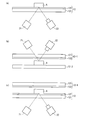
図5(a)(b)は、実施形態4にかかる計測装置の構成例を示す図である。図5(a)及び図5(b)に示す計測装置は、試料Aを載置する透明部材12と、試料Aに光を照射する光照射部21と、試料Aからの光を検出する光検出部22と備える。
図5(a)(b)は、実施形態4にかかる計測装置の構成例を示す図である。図5(a)及び図5(b)に示す計測装置は、試料Aを載置する透明部材12と、試料Aに光を照射する光照射部21と、試料Aからの光を検出する光検出部22と備える。
図5(a)に示す例では、光照射部21は、透明部材12の試料載置面の対向する面側に設けられ、透明部材12を介して、光を試料Aへ照射する。光検出部22は、透明部材12の試料載置面側に設けられ、光照射部21から出て透明部材12及び試料Aを順に透過した光を検出する。光検出部22は、試料Aの透視画像を取得することができる。
図5(b)に示す例では、光照射部21は、透明部材12の試料載置面側に設けられ、試料Aへ向けて直接光を照射する。光検出部22は、透明部材12の試料載置面に対向する面側に設けられ、光照射部21から出て試料A及び透明部材12を順に透過した光を検出する。
なお、図5(a)及び図5(b)においても、図示しないが、図1(a)と同様に、透明導電膜122上の両端に設けられた電極41a、41b、透明部材12の温度を測定する熱電対43、電極41a、41b間の電圧を制御する熱制御部42、並びに熱制御部42及び光検出部22を制御するコンピュータ1が設けられてもよい。また、本実施形態の透明部材12も、図1(b)に示すように、導電性を有する透明基板で形成することができる。
本実施形態は、光照射部21と光検出部22が透明部材12を挟んで対向して配置される場合の例である。本実施形態のように、光照射部または光検出部の少なくともいずれかと試料との間に透明部材を配置することで、熱の伝達効率を向上させ、かつ装置を簡素にすることが可能になる。
(実施形態5)
図6(a)は、実施形態5にかかる計測装置の構成例を示す図である。図6(a)に示す計測装置は、透明部材12の上に載置された試料Aに光を照射する光照射部21と、試料Aから光を検出することにより、試料Aを撮影する光検出部22とを備える。また、透明部材12は、実施形態1と同様に、透明基板121及び透明導電膜122を備える。
図6(a)は、実施形態5にかかる計測装置の構成例を示す図である。図6(a)に示す計測装置は、透明部材12の上に載置された試料Aに光を照射する光照射部21と、試料Aから光を検出することにより、試料Aを撮影する光検出部22とを備える。また、透明部材12は、実施形態1と同様に、透明基板121及び透明導電膜122を備える。
光照射部21及び光検出部22は、透明部材12の試料Aの載置面と対向する面側に配置される。そのため、光照射部21の照射光は、透明部材12を介して試料Aへ到達する。試料Aで散乱した光は、透明部材12を通って光検出部22へ到達し、検出される。このように、試料Aを保持しかつ発熱手段を有する透明部材12越しに、光を照射し、透明部材12越しに試料Aからの光を検出する構成とすることで、装置構成が簡素化される。また、熱源を試料Aの近くに配置することができるので、熱への変換効率もよくなり、消費電力も抑えることができる。
図6(b)は、本実施形態の変形例を示す図である。図6(b)に示す例では、試料Aを設置するテーブル12-2を上部に、試料のための空間をはさんで透明部材12-1が設けられる。透明部材12-1の透明導電膜122が形成された面が、テーブル12-2すなわち試料に対向するように、透明部材12-1が配置される。光照射部21及び光検出部22は、透明部材12-1のさらに上部に配置される。すなわち、テーブル12-2と、光照射部21及び光検出部22との間に透明導電膜122を有する透明部材12-1が配置される。光照射部21は、透明部材12-1を介して試料に光を照射し、光検出部22は、透明部材12-1を介して試料を撮影することができる。図6(b)に示す構成によっても、熱源を試料Aに近づけて熱の伝達効率を向上させるとともに、計測装置を簡素することができる。また、図6(b)では、試料Aの空間をテーブル12-2と透明部材12-1で挟む構成であるため、試料A周辺からの熱の発散が抑えられる。なお、試料Aを載置するテーブル12-1は、透明でなくてもよい。
図6(c)に示す計測装置は、図6(a)に示す構成に、さらに、試料Aの上部の空間を覆う透明部材12-1を設けた構成である。透明部材12-1の試料側の面には、透明導電膜122が形成されている。この構成により、試料Aを保持する面と試料Aの上部の空間を覆う面の双方に熱源を配置することができる。これにより、試料Aを急速に熱することができる。また、試料Aの上下を発熱体で挟む構成なので、試料Aの周りの空間から熱が発散するのを抑えることができる。なお、試料の上に設けられる透明部材12-1は、必ずしも透明でなくてもよい。
図6(a)~図6(c)においても、図示しないが、図1(a)と同様に、透明導電膜122上の両端に設けられた電極41a、41b、透明部材12の温度を測定する熱電対43、電極41a、41b間の電圧を制御する熱制御部42、並びに熱制御部42、光照射部21及び光検出部22を制御するコンピュータ1が設けられてもよい。また、本実施形態の透明部材12及び透明部材12-1の少なくとも1つは、図1(b)に示すように、導電性を有する透明基板で形成することができる。
また、図6(a)~図6(c)の構成において、光照射部21は、透明部材12の上面に載せられた試料Aに対して、透明部材12の下面から、光の強度が周期的に変化する光パターンを照射することができる。この場合、光検出部22は、光パターンが照射された試料Aを、透明部材12の下面から撮影する。コンピュータ1の画像処理部52は、光検出部22で撮影された試料Aの画像を処理して、試料の表面の3次元形状を表す表面形状データを生成する。例えば、光照射部21によりサインカーブ等の光パターンを、位相をずらしながら試料Aに照射し、光検出部22が位相がずれた光パターンの画像を複数回に渡って撮影することができる。画像処理部52は、位相がずれた光パターンを照射された試料の複数の画像を基に、位相シフト法を用いて試料Aの3次元形状を算出することができる。位相シフト法を用いた3次元計測の具体例は、実施形態6で後述する。
本実施形態は、レーザやパターン等を試料に照射し、試料からの光を観測することで距離を計測するアクティブ方式を用いた3次元計測装置に好適に用いることができる。例えば、図6(a)(c)に示す計測装置は、透明導電膜が設けられた透明部材の上面に試料を配置し、透明部材の下面から光を照射し、試料で反射した光を下面で観測する構成である。これにより、試料の配置面(熱発生面)からの距離を高精度で計測することができるとともに、簡単な構成で試料の温度制御が可能になる。
なお、アクティブ方式を用いた計測法の例として、上記パターン投影法の他、レーザによる光切断方式、レーザによるタイムオブフライト(TOF : time of flight)法、共焦点法、照度差ステレオ法等が挙げられる。また、パターン投影法には、上記位相シフト法の他に、例えば、格子パターン投影法、空間コード化法、ランダムパターン投影法、モアレ法、干渉法等が含まれる。これらはいずれも、本実施形態に適用可能である。
(変形例)
図7は、図6(a)に示す計測装置の変形例を示す図である。図7に示す例では、透明部材12において、透明基板121の上面に全体ではなく一部に透明導電膜122が形成されている。具体的には、試料Aが載置される領域以外の領域に透明導電膜122が形成される。このように、試料Aが載置される領域において透明導電膜122を除去することにより、試料Aが直接、発熱体である透明導電膜122に接するのを避けることができる。例えば、試料Aが樹脂等であり、発熱する透明導電膜122に触れると溶解する可能性がある場合等に図7に示す構成は有効である。
図7は、図6(a)に示す計測装置の変形例を示す図である。図7に示す例では、透明部材12において、透明基板121の上面に全体ではなく一部に透明導電膜122が形成されている。具体的には、試料Aが載置される領域以外の領域に透明導電膜122が形成される。このように、試料Aが載置される領域において透明導電膜122を除去することにより、試料Aが直接、発熱体である透明導電膜122に接するのを避けることができる。例えば、試料Aが樹脂等であり、発熱する透明導電膜122に触れると溶解する可能性がある場合等に図7に示す構成は有効である。
透明導電膜122のパターニングは、例えば、透明基板121の上面全体に透明導電膜を成膜した後、フォトレジストを用いたエッチングによりパターン形成することでできる。また、透明電極膜122のパターンは、図7に示す例に限られない。例えば、試料Aの領域のみを加熱するために、試料Aの載置領域及びその周辺のみに透明導電膜122を形成することもできる。これにより、加熱に使う消費電力を低減することができる。
図8は、図6(a)に示す計測装置の他の変形例を示す図である。図8に示す例では、試料Aを含む空間を密閉するためのカバー61が設けられる。これにより、熱効率を向上させることができる。また、外気の影響で試料Aの温度が不安定になるのを防ぐことができる。
なお、図7、図8に示す変形例は、上記実施形態1~4及び下記実施形態6にも適用することができる。例えば、図8に示す透明部材12は、図1(b)のように、導電性を有する透明基板で形成することもできる。
(実施形態6)
図9は、実施形態6にかかる検査装置の構成例を示す図である。上記実施形態5における計測装置を、検査装置に適用した場合の詳細な実施形態である。
図9は、実施形態6にかかる検査装置の構成例を示す図である。上記実施形態5における計測装置を、検査装置に適用した場合の詳細な実施形態である。
[検査システムの構成]
図9示す検査装置100は、試料の形状を測定する測定部5と、測定部5を制御する制御部4と、測定部5及び制御部4へ接続されるコンピュータ1と備える。コンピュータ1には、モニタ2並びに入力デバイス3(マウス3a及びキーボード3b)が接続されている。図9に示す検査装置100は、試料の形状を測定し、形状の良否を判定する装置である。測定部5が制御部4による制御されて試料(検査対象物)の表面形状を測定し、コンピュータ1が測定データに基づいて試料の形状の良否を判定し、結果(検査結果)を保存または出力する。コンピュータ1は、上記実施形態1と同様に、計測制御部51、画像処理部52、判定部53を含む演算部50を備える(図1参照)。例えば、電子部品の生産ラインにおいて、完成した電子部品の形状の良否を判定するのに検査装置100を用いることができる。以下、検査装置100が電子部品の形状判定に用いられる場合について説明するが、検査装置100の試料は電子部品に限られない。
図9示す検査装置100は、試料の形状を測定する測定部5と、測定部5を制御する制御部4と、測定部5及び制御部4へ接続されるコンピュータ1と備える。コンピュータ1には、モニタ2並びに入力デバイス3(マウス3a及びキーボード3b)が接続されている。図9に示す検査装置100は、試料の形状を測定し、形状の良否を判定する装置である。測定部5が制御部4による制御されて試料(検査対象物)の表面形状を測定し、コンピュータ1が測定データに基づいて試料の形状の良否を判定し、結果(検査結果)を保存または出力する。コンピュータ1は、上記実施形態1と同様に、計測制御部51、画像処理部52、判定部53を含む演算部50を備える(図1参照)。例えば、電子部品の生産ラインにおいて、完成した電子部品の形状の良否を判定するのに検査装置100を用いることができる。以下、検査装置100が電子部品の形状判定に用いられる場合について説明するが、検査装置100の試料は電子部品に限られない。
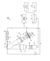
図9に示すように、測定部5は、投影プロジェクタ21(光照射部の一例)、光検出部22、テーブル12、テーブル12を動かす駆動部13、及びテーブル12の温度を制御する温度制御部41を備える。テーブル12は、上記実施形態1における透明部材12と同様に構成することができる。すなわち、テーブル12は、透明なガラス板である透明基板121と、その上面に形成された透明導電膜122と、透明導電膜122上の両端に形成された電極41a、41bを備える。テーブル12は、測定部5の筐体の上面に設けられる。テーブル12に上面に試料Aが載せられる。テーブル12の下には、投影プロジェクタ21及び光検出部22が設けられる。投影プロジェクタ21は、テーブル12の下面から縞模様の光パターンを試料Aへ照射する。光検出部22は、テーブル12の下面から試料Aに投影された光パターンを撮影する。
図9に示す検査装置100は、3次元形状の取得に、三角測量に分類される格子投影法を用いる。縞模様の光パターンを、試料Aに投影した場合、縞模様は試料Aの形状にあわせて変形するので、その試料Aの画像における縞模様の変形量を測定することで形状を測定することができる。以下、検査装置100の各部について、詳細に説明する。
テーブル12の上面は、試料Aを設置する面(以下、試料面12aと称する)である。ここでは、試料面12a内で互いに直行する軸をXY軸とし、試料面12aに垂直な軸をZ軸とする。駆動部13は、X軸方向及びY軸方向にテーブル12を移動させるXY駆動部13と、Z軸方向にテーブル12を移動させるZ駆動部13とを備えてもよい。また、テーブル12を移動させる構成に換えて、投影プロジェクト21及び光検出部22を移動させる構成にすることもできる。また、テーブル12の温度は、温度制御部42によってコンピュータ1から指定された温度になるように制御される。
投影プロジェクタ21は、試料面12aの向こう側の試料Aに、光の強度が周期的に変化する縞状の光パターンを照射するユニットである。そのため、投影プロジェクタ21では、例えば、光源6、集光レンズ7、グリッド8、テレセントリックレンズ9、10が順に並べて配置される。
光源6には、例えば、コストの観点からLEDが好ましく用いられる。光源6には、その他、ハロゲンランプ、レーザ光源等を用いることができる。集光レンズ7は、光源6の光を集光し平行光に近づける。グリッド8は、この平行光に近い光を、強度が周期的に変化する縞状の光にする。
グリッド8は、例えば、正弦波または余弦波のパターンを有するフィルムを備える。フィルムとして、例えば、波長が50μm~500μm程度の正弦波パターンの格子フィルムを用いることができる。
なお、グリッドの格子パターンは、明及び暗の2種類の強度が交互に現れる格子パターンでもよいし、明から暗、暗から明への変化に余弦波または正弦波に相当する光の強弱を持たせるパターンであってもよい。このように余弦波または正弦波の強度変化を有する光を試料Aへ投影することで、光検出部22で撮影する全ての画素で高さ解析を行うことができる。また、光パターンは、多重の輪の模様でもよいし市松模様でもよい。
また、光パターンを生成する手段は、上記のフィルムに限られない。例えば、液晶パネルを用いて、強度が周期的に変化する縞状の光パターンを生成することもできる。
また、グリッド8にステッピングモータを設けることにより、光パターンの縞の位置を移動(シフト)させることができる。ステッピングモータによるグリッド8の駆動は、例えば、制御部4からの信号により制御される。例えば、制御部4または測定部5に、マイクロステッピングモータを駆動するマイクロステッピングドライバを設けることができる。マイクロステッピングドライバを用いることにより、高分解能の光パターンシフトが可能になる。なお、コンピュータ1は、制御部4に対してグリッド8の駆動条件の設定をすることができる。
グリッド8を通った、縞状の光パターンは、テレセントリックレンズユニット11を通って、試料面12a上の試料Aに照射される。テレセントリックレンズユニット11は、テレセントリックレンズ9、10によりテレセントリック光学系を形成している。テレセントリックレンズ9、10により形成されるテレセントリック光学系は、像側テレセントリック光学系、物体側テレセントリック光学系、または両側テレセントリック光学系とすることができる。例えば、両側テレセントリック光学系の場合は、物体側、像側とも主交線がレンズ光軸Kに平行になるように、テレセントリックレンズ9、10が配置される。
テレセントリックレンズユニット11を出た光による像では、被写深度内で、被写体寸法が変化しにくい。すなわち、テレセントリックレンズユニット11から出た光における縞の間隔は、光進行方向においてほとんど変化しない。そのため、後段における、光パターン照射され試料Aの画像の処理において、縞の間隔変化を補正する処理が不要になる。
光検出部22は、CCDカメラ15、テレセントリックレンズユニット17を備える。テレセントリックレンズユニット17は、テレセントリックレンズ16、18を含む。CCDカメラ15は、縞状の光パターンが照射された試料Aを撮影する。なお、撮像装置は、CCDカメラ15に限られず、例えば、CMOSセンサ、ラインセンサ等を用いることもできる。CCDカメラ15は、テレセントリックレンズユニット17を通った光による画像を撮影するので、縞間隔の補正が不要な画像が得ることができる。
このように、本実施形態の測定部5は、光源6、グリッド8、テレセントリックレンズユニット11を含む投影プロジェクタ21と、CCDカメラ15、テレセントリックレンズユニット17を含む光検出部22とを組み合わせ構成なので、水平分解能及び高さ分解能が数ミクロンレベルの高分解能の3次元情報を取得することが可能になる。そのため、上記の測定部5により、例えば、電子部品の端子等の評価に適した3次元形状データ(表面形状データ)を得ることができる。
なお、測定部5の構成は、図9に示す構成に限られない。例えば、異なる方向から光パターンを照射する複数の投影プロジェクタを備える構成であってもよい。また、光検出部22は、必ずしもテレセントリック光学系を用いる必要はない。例えば、光検出部22は、光進行方向において幅が広がっていく光パターンを照射することで、投影面を広くとることもできる。また、光検出部22は、グリッドを投影面に対して傾けることなく光パターンを投影するアオリ投影をする構成であってもよい。また、テーブル12は、図1(b)に示すように導電性を有する透明基板で形成することもできる。
[表面形状データの計算例]
次に、格子投影法を用いて試料Aの表面形状データを計算する方法について説明する。図10は、測定部5における試料Aへの縞状の光パターンの投影及び撮影の様子を模式的に表した図である。図10(a)に示すように、投影プロジェクタ21からは、矢印D方向において強度が周期的に変化する縞状の光パターンが試料Aへ照射される。図3(b)は、縞状パターンの一例を示す図である。試料面においては、Y軸方向において周期的に強度が変化する縞状の模様が投影される。試料Aの表面においては、試料Aの表面形状に応じて縞状の模様は変形する。図3(c)は、光検出部22で撮影される画像の一例を示す図である。試料Aの表面形状に合わせて縞模様が変形している様子が画像に表れる。縞模様の変形量xと試料Aの高さhとの関係は、試料面12aに対する光の投影各をαとすると、h=x/tanαで計算される(図3(d))。
次に、格子投影法を用いて試料Aの表面形状データを計算する方法について説明する。図10は、測定部5における試料Aへの縞状の光パターンの投影及び撮影の様子を模式的に表した図である。図10(a)に示すように、投影プロジェクタ21からは、矢印D方向において強度が周期的に変化する縞状の光パターンが試料Aへ照射される。図3(b)は、縞状パターンの一例を示す図である。試料面においては、Y軸方向において周期的に強度が変化する縞状の模様が投影される。試料Aの表面においては、試料Aの表面形状に応じて縞状の模様は変形する。図3(c)は、光検出部22で撮影される画像の一例を示す図である。試料Aの表面形状に合わせて縞模様が変形している様子が画像に表れる。縞模様の変形量xと試料Aの高さhとの関係は、試料面12aに対する光の投影各をαとすると、h=x/tanαで計算される(図3(d))。
ここで、さらに高精度に測定を行うために位相解析には位相シフト法を適用することができる。位相シフト法による測定では、投影プロジェクタ21が投影する縞模様を1/4周期ずつシフトさせ4枚の縞画像を撮影し、位相解析を行う。
図11は、図9に示す検査装置100が、位相シフト法を用いて試料Aの3次元測定をする処理の一例を示すフローチャートである。図9に示す例では、試料Aを試料面12aにセットすると(S1)、温度制御部42により、テーブル12の温度がコンピュータ1で設定された温度になるよう調整される(S2)。テーブル12の温度が設定温度に達すると、温度制御部42はその旨を通知する信号をコンピュータ1に送る。コンピュータ1は、テーブル12の温度が設定温度に達した旨の通知を受けると、制御部4に対して、測定開始の指示を出す。制御部4は、測定部5を制御して測定を開始する。
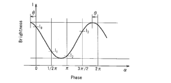
まず、測定部5において、縞模様(格子パターン)の光がテーブル12の下から試料Aへ照射される。これにより、格子パターンが試料Aへ投影される。この格子パターンが投影された試料Aの画像が光検出部22によりテーブル12の下面から撮影される(S3)。ここでは、光の強度が余弦波に相当する変化を示す縞模様の光が照射される場合を説明する。この撮影された画像には、試料Aの表面形状に応じて変形した縞模様が写っている。また、投影プロジェクタ21は、余弦波の縞模様を1/4周期ずつシフトさせた光をそれぞれ投影し、光検出部22は、4枚の位相が1/4周期ずつシフトした縞模様の画像を撮影する。ここで、測定部5で撮影された画像のデータは、コンピュータ1の画像処理部(後述)へ送られる。コンピュータ1の画像処理部52は、前記画像のデータを処理することで、位相解析を行う(S4)。位相解析では、画像中の各画素の位置(座標(x、y))において投影された光パターンの位相θを計算する。位置(x、y)における明るさは、下記式(1)で表される。

aは、その位置での縞の明るさの振幅を示す係数であり、bは、その位置での明るさのオフセット量を示す係数である。図12は上記式(1)を表すグラフである。図12に示すように、4枚の画像上の同じ位置(x、y)での明るさI0、I1、I2、I3は、下記式(2)で表される。

したがって、(x、y)における位相θは、下記式(3)により計算することができる。

上記式(3)に示す位相θは、係数a、bによらない。このように、縞の明るさの振幅a項と明るさのオフセット量b項が計算式上でキャンセルされる為、外乱光の影響を受けにくく、高精度な測定が可能になる。そのため、位相シフト法を用いることにより、電子部品の端子の形状検査のような細かい検査に適した精度の測定が可能になる。
このようにして各位置(x、y)の位相θが計算される。位相θが等しい点を結んで得られる線(等位相線)には、図3(c)に示した縞模様と同様に、試料Aの形状に応じた変計量が現れる。そのため、各位置における位相θの変形量(位相差)を計算し(図11のS5)、この位相差を高さ単位に変換する(S6)ことにより、各位置における試料Aの高さを示す値が得られる。すなわち、試料Aの表面の3次元形状を示すデータが得られる。
なお、処理S5において、各位置の位相θが試料Aによりどの程度変化しているかを示す位相差を計算する際には、予めコンピュータ1に記録された基準位相データを用いる。例えば、試料Aが置かれていない試料面12aに同じ余弦波の縞模様を投影した場合の画像を予め撮影し、試料面12aにおける各位置の位相θを示すデータを算出して、基準位相データとして記録することができる。コンピュータ1は、この試料面12aの各位置の位相θを表す基準位相データと、試料Aを置いた場合の各位置の位相θを表すデータとの差を計算することにより、位相差を計算することができる。各位置の位相差は、試料Aの表面と試料面12aとの距離(高さ)に応じた値であるので、高さを示すデータに変換することができる(S6)。
本実施形態では、試料Aがテーブル12の上面に置かれた状態で光パターンの投影及び撮影がなされるので、テーブル12の上面からの浮き量を、高さ情報として求めることができる。そのため、例えば、テーブル12の上面を実装基板に仮定して、電子部品の実装時の浮き量を判定することが可能になる。さらに、テーブル12は、透明導電膜122を備えるので、実装面の温度を任意に設定することができる。そのため、実際に実装されるときとほぼ同じ状態で電子部品の実装面側を計測することができる。これにより、電子部品の実装時のバランス及び実装時に想定される温度を考慮した計測が可能になる。
以上のとおり、位相シフト法では、試料Aへ照射される光パターンにおける強度変化の位相を異ならせて、それぞれの位相に対応する複数の画像のデータを取得する。この複数の画像の同じ位置(x、y)における明るさを用いて、その位置(x、y)に投射された光パターンの位相θを求め、この位相θを基に三角測量の原理を用いて高さを計算する。
なお、位相シフト法を用いた高さ情報の取得方法は、上記例に限られない。例えば、撮影する画像は4枚に限られない。3枚撮影すれば位相θの計算は可能であるし、4枚以上の画像を撮影して精度を高めることもできる。また、位相θの計算に用いる上記式(1)~(3)も一例であり、その他の式を用いて位相θを計算することができる。
このようにして位相シフト法を用いて得られた、試料Aの表面の3次元形状を示すデータを、コンピュータ1が処理することで、試料Aの検査が判定部52により実行される(S7)。例えば、上記のように画像処理部52が、試料Aの突起部の試料面12aに対する位置(高さ情報)を算出し、判定部53が、その位置が所定の範囲内であるか否かを判定することにより、突起を有する試料の良否を判断することができる。
検査装置100は、例えば、ICチップのような、少なくとも1方向に並ぶ複数の突起部を備える試料を検査することができる。ICチップを基板に実装する場合、ICチップが有する複数の足(突起部)が基板に確実に接続されることが要求される。そのため、検査装置100では、テーブル12の試料面12aにおかれたICチップを特定の温度に加熱した状態で、突起部それぞれのテーブル12の試料面12aに対する位置を測定し、突起部の位置が所定の範囲内であるか否かを判定することができる。これにより、特定の温度下で、ICチップを基板に実装できるか否かを検査することができる。
上記の検査装置100は、透明導電膜122を表面に形成されたテーブル12または導電性を有する透明基板で形成されたテーブル12に試料Aをおいた状態で、試料Aの温度を制御し、さらに試料Aの下面からの光パターンの照射及び試料Aの撮影が可能になる。試料Aをテーブル12に置くという動作だけで、特定温度での形状の検査が可能になる。このように、本実施形態によれば、試料Aの設置作業も、装置の構成も簡素にでき、さらに、温度制御下で高速に試料の形状を測定することが可能になる。また、セラミック基板、フレキシブル基板等に実装される電子部品を計測する場合、テーブル12上面を実装面として、実装時の状態とほぼ同じ状態で計測することが可能になる。すなわち、実装時の試料の状態を模擬することができる。
すなわち、透明導電膜122を有する透明部材を使ったテーブル12と上記のようなパターン投影法を用いた3次元形状測定器の組み合わせにより、電子部品の端子の検査に適した3次元測定が可能になる。例えば、大量の電子部品の耐熱性を素早く検査することが可能になる。さらに、位相シフトを用いることで、高さ情報を効率よく迅速に処理し、高精度の解析結果を得ることができる。以上のとおり、本実施形態によれば、例えば、電子機器の生産ラインにおける検査に適した構造の測定器及び計算処理が提供される。
なお、本発明の適用範囲は、上記実施形態に限られない。例えば、試料は、電子部品に限定されない。また、上記実施形態では、測定器として、格子投影法を用いた3次元形状測定器を用いた場合を説明したが、測定器は、例えば、上記以外のパターン投影法(例えば、グレースケールのパターンやカラーパターン等を投影する方法)や、モアレ、焦点法、ステレオ法、その他の方法を用いた3次元測定器であってもよい。
以上、上記の実施形態1~6における計測装置または検査装置は、加熱装置として透明導電膜を用いる。そのため、従来の装置に比べ装置構成が簡素化される。また、温度コントロールも容易にできる。さらに、熱への変換効率もよいことから消費電力も抑えることができる。
1 コンピュータ
2 モニタ
3 入力デバイス
4 制御部
5 測定部
6 光源
7 集光レンズ
8 グリッド
9 テレセントリックレンズ
10 画像処理部
11 テレセントリックレンズユニット
12 透明部材(テーブル)
12a 試料面
121 透明基板
122 透明導電膜
13 駆動部
15 カメラ
16 テレセントリックレンズ
17 テレセントリックレンズユニット
21 光照射部(投影プロジェクタ)
22 光検出部
30 電子部品
31 本体
32a-32e 端子
50 演算部
51 計測制御部52
52 画像処理部
53 判定部
100 検査装置
2 モニタ
3 入力デバイス
4 制御部
5 測定部
6 光源
7 集光レンズ
8 グリッド
9 テレセントリックレンズ
10 画像処理部
11 テレセントリックレンズユニット
12 透明部材(テーブル)
12a 試料面
121 透明基板
122 透明導電膜
13 駆動部
15 カメラ
16 テレセントリックレンズ
17 テレセントリックレンズユニット
21 光照射部(投影プロジェクタ)
22 光検出部
30 電子部品
31 本体
32a-32e 端子
50 演算部
51 計測制御部52
52 画像処理部
53 判定部
100 検査装置
Claims (6)
- 計測対象の試料を保持する位置または前記試料に対向する位置に配置され、導電性を有する透明部材と、
前記試料からの光を検出する光検出部と、
前記透明部材に印加する電圧を制御することにより、前記透明部材の温度を制御する熱制御部とを備えた、計測装置。 - 前記透明部材は、前記試料を載せるための試料テーブルも兼ねている、請求項1に記載の計測装置。
- 前記光検出部は、前記試料テーブルの下側に配置され、前記透明部材の上面に載せられた前記試料からの光を前記透明部材の下面から検出する、請求項2に記載の計測装置。
- 前記試料に光を照射する光照射部をさらに備え、
前記透明部材は、前記光照射部及び前記光検出部の少なくともいずれかと前記試料の設置位置との間に配置される、請求項1~3のいずれか1項に記載の計測装置。 - 前記光検出部は、前記熱制御部により前記透明部材が所定の温度になったときに、前記試料からの光を検出する、請求項1~4のいずれか1項に記載の計測装置。
- 前記光検出部により得られた画像を基に、当該試料が所定の基準を満たしているかを判定する演算部をさらに備える、請求項1~5のいずれか1項に記載の計測装置。
Priority Applications (1)
| Application Number | Priority Date | Filing Date | Title |
|---|---|---|---|
| PCT/JP2012/063197 WO2013175590A1 (ja) | 2012-05-23 | 2012-05-23 | 計測装置 |
Applications Claiming Priority (1)
| Application Number | Priority Date | Filing Date | Title |
|---|---|---|---|
| PCT/JP2012/063197 WO2013175590A1 (ja) | 2012-05-23 | 2012-05-23 | 計測装置 |
Publications (1)
| Publication Number | Publication Date |
|---|---|
| WO2013175590A1 true WO2013175590A1 (ja) | 2013-11-28 |
Family
ID=49623321
Family Applications (1)
| Application Number | Title | Priority Date | Filing Date |
|---|---|---|---|
| PCT/JP2012/063197 WO2013175590A1 (ja) | 2012-05-23 | 2012-05-23 | 計測装置 |
Country Status (1)
| Country | Link |
|---|---|
| WO (1) | WO2013175590A1 (ja) |
Cited By (2)
| Publication number | Priority date | Publication date | Assignee | Title |
|---|---|---|---|---|
| WO2019207267A1 (fr) * | 2018-04-27 | 2019-10-31 | Insidix | Dispositif de mesure topographique |
| EP4123258A1 (en) * | 2021-07-22 | 2023-01-25 | Siemens Corporation | Planar object segmentation |
Citations (5)
| Publication number | Priority date | Publication date | Assignee | Title |
|---|---|---|---|---|
| JPH10321539A (ja) * | 1997-05-22 | 1998-12-04 | Hitachi Ltd | 半導体製造方法および製造装置 |
| JPH11230903A (ja) * | 1998-02-10 | 1999-08-27 | Fuji Photo Film Co Ltd | 液体の屈折率測定方法および装置 |
| JP2004343003A (ja) * | 2003-05-19 | 2004-12-02 | Fuji Photo Film Co Ltd | 露光装置 |
| WO2007066687A1 (ja) * | 2005-12-06 | 2007-06-14 | Nikon Corporation | 温度計測方法、露光方法、露光装置、及びデバイス製造方法 |
| JP2008261679A (ja) * | 2007-04-11 | 2008-10-30 | Nikke Kikai Seisakusho:Kk | 形状検査装置 |
-
2012
- 2012-05-23 WO PCT/JP2012/063197 patent/WO2013175590A1/ja active Application Filing
Patent Citations (5)
| Publication number | Priority date | Publication date | Assignee | Title |
|---|---|---|---|---|
| JPH10321539A (ja) * | 1997-05-22 | 1998-12-04 | Hitachi Ltd | 半導体製造方法および製造装置 |
| JPH11230903A (ja) * | 1998-02-10 | 1999-08-27 | Fuji Photo Film Co Ltd | 液体の屈折率測定方法および装置 |
| JP2004343003A (ja) * | 2003-05-19 | 2004-12-02 | Fuji Photo Film Co Ltd | 露光装置 |
| WO2007066687A1 (ja) * | 2005-12-06 | 2007-06-14 | Nikon Corporation | 温度計測方法、露光方法、露光装置、及びデバイス製造方法 |
| JP2008261679A (ja) * | 2007-04-11 | 2008-10-30 | Nikke Kikai Seisakusho:Kk | 形状検査装置 |
Cited By (4)
| Publication number | Priority date | Publication date | Assignee | Title |
|---|---|---|---|---|
| WO2019207267A1 (fr) * | 2018-04-27 | 2019-10-31 | Insidix | Dispositif de mesure topographique |
| FR3080677A1 (fr) * | 2018-04-27 | 2019-11-01 | Insidix | Dispositif de mesure topographique |
| US11365965B2 (en) | 2018-04-27 | 2022-06-21 | Insidix | Topographic measurement device |
| EP4123258A1 (en) * | 2021-07-22 | 2023-01-25 | Siemens Corporation | Planar object segmentation |
Similar Documents
| Publication | Publication Date | Title |
|---|---|---|
| JP5709009B2 (ja) | 三次元計測装置 | |
| JP6027220B1 (ja) | 三次元計測装置 | |
| KR101640935B1 (ko) | 3차원 형상 측정장치 | |
| TW201033579A (en) | Three dimensional measuring device | |
| JP5847568B2 (ja) | 三次元計測装置 | |
| JP2013124938A (ja) | 三次元計測装置 | |
| US9594028B2 (en) | Method and apparatus for determining coplanarity in integrated circuit packages | |
| TW201221901A (en) | Method and device for evaluating surface shape | |
| JP5674453B2 (ja) | 計測装置 | |
| WO2018171031A1 (zh) | 三相机组特征点匹配方法、测量方法及三维检测装置 | |
| WO2013175590A1 (ja) | 計測装置 | |
| CN102628678B (zh) | 三维测量装置、三维测量方法 | |
| TW201231914A (en) | Surface shape evaluating method and surface shape evaluating device | |
| KR101528200B1 (ko) | 3차원 열영상 측정 장치 및 방법 | |
| JP6781969B1 (ja) | 測定装置及び測定方法 | |
| KR102122275B1 (ko) | 배광 특성 측정 장치 및 배광 특성 측정 방법 | |
| JP2006064669A (ja) | 仮想接面測定用の干渉計装置 | |
| JP2013250098A (ja) | 配線欠陥検出方法および配線欠陥検出装置、並びに配線基板の製造方法 | |
| JP4947559B2 (ja) | 三次元計測装置 | |
| JP2012242134A (ja) | 形状測定装置およびこれに用いる光学フィルタ | |
| TWI769423B (zh) | 一種光罩姿態監測方法、裝置及光罩顆粒度檢測設備 | |
| JP7030079B2 (ja) | 三次元計測装置及び三次元計測方法 | |
| WO2016203668A1 (ja) | 三次元計測装置 | |
| TWI580927B (zh) | Three - dimensional measuring device and three - dimensional measurement method | |
| JP6062523B1 (ja) | 三次元計測装置 |
Legal Events
| Date | Code | Title | Description |
|---|---|---|---|
| 121 | Ep: the epo has been informed by wipo that ep was designated in this application |
Ref document number: 12877598 Country of ref document: EP Kind code of ref document: A1 |
|
| NENP | Non-entry into the national phase |
Ref country code: DE |
|
| 32PN | Ep: public notification in the ep bulletin as address of the adressee cannot be established |
Free format text: NOTING OF LOSS OF RIGHTS PURSUANT TO RULE 112(1) EPC (EPO FORM 1205A DATED 04.03.2015) |
|
| NENP | Non-entry into the national phase |
Ref country code: JP |
|
| 122 | Ep: pct application non-entry in european phase |
Ref document number: 12877598 Country of ref document: EP Kind code of ref document: A1 |