WO2013161781A1 - Contactless information medium and booklet with included contactless information medium - Google Patents
Contactless information medium and booklet with included contactless information medium Download PDFInfo
- Publication number
- WO2013161781A1 WO2013161781A1 PCT/JP2013/061823 JP2013061823W WO2013161781A1 WO 2013161781 A1 WO2013161781 A1 WO 2013161781A1 JP 2013061823 W JP2013061823 W JP 2013061823W WO 2013161781 A1 WO2013161781 A1 WO 2013161781A1
- Authority
- WO
- WIPO (PCT)
- Prior art keywords
- information medium
- chip
- type information
- contact type
- antenna
- Prior art date
Links
Images


Classifications
-
- G—PHYSICS
- G06—COMPUTING; CALCULATING OR COUNTING
- G06K—GRAPHICAL DATA READING; PRESENTATION OF DATA; RECORD CARRIERS; HANDLING RECORD CARRIERS
- G06K19/00—Record carriers for use with machines and with at least a part designed to carry digital markings
- G06K19/06—Record carriers for use with machines and with at least a part designed to carry digital markings characterised by the kind of the digital marking, e.g. shape, nature, code
- G06K19/067—Record carriers with conductive marks, printed circuits or semiconductor circuit elements, e.g. credit or identity cards also with resonating or responding marks without active components
- G06K19/07—Record carriers with conductive marks, printed circuits or semiconductor circuit elements, e.g. credit or identity cards also with resonating or responding marks without active components with integrated circuit chips
- G06K19/077—Constructional details, e.g. mounting of circuits in the carrier
- G06K19/07749—Constructional details, e.g. mounting of circuits in the carrier the record carrier being capable of non-contact communication, e.g. constructional details of the antenna of a non-contact smart card
-
- G—PHYSICS
- G06—COMPUTING; CALCULATING OR COUNTING
- G06K—GRAPHICAL DATA READING; PRESENTATION OF DATA; RECORD CARRIERS; HANDLING RECORD CARRIERS
- G06K19/00—Record carriers for use with machines and with at least a part designed to carry digital markings
- G06K19/06—Record carriers for use with machines and with at least a part designed to carry digital markings characterised by the kind of the digital marking, e.g. shape, nature, code
- G06K19/067—Record carriers with conductive marks, printed circuits or semiconductor circuit elements, e.g. credit or identity cards also with resonating or responding marks without active components
- G06K19/07—Record carriers with conductive marks, printed circuits or semiconductor circuit elements, e.g. credit or identity cards also with resonating or responding marks without active components with integrated circuit chips
- G06K19/077—Constructional details, e.g. mounting of circuits in the carrier
- G06K19/0772—Physical layout of the record carrier
- G06K19/07722—Physical layout of the record carrier the record carrier being multilayered, e.g. laminated sheets
Definitions
- the present invention relates to a non-contact type information medium that includes an antenna and an IC (integrated circuit) chip and can record information on the IC chip in a non-contact manner, and a booklet including the non-contact type information medium.
- a non-contact type information medium that includes an antenna and an IC (integrated circuit) chip and can record information on the IC chip in a non-contact manner, and a booklet including the non-contact type information medium.
- a booklet attached to a non-contact type information medium in which a non-contact type information medium is added to a booklet-shaped information medium such as a passport or a savings passbook has been developed.
- the non-contact type information medium used for such a non-contact type information medium-attached booklet has a configuration in which an IC inlet including an antenna and a non-contact IC chip connected to the antenna is sandwiched between outer packaging substrates.
- the booklet attached to the non-contact type information medium is bound by sticking the non-contact type information medium to a cover member called a cover cloth or the like, and further attaching a booklet such as an inner sheet or a body sheet.
- Such a booklet attached to a non-contact type information medium has a feature that data can be printed or a VISA stamp can be added like an ordinary booklet, and electronic data can be recorded.
- a booklet having a non-contact type information medium inside the back cover as described above is disclosed in, for example, Document 1 (Japanese Patent Laid-Open No. 2002-04068).
- the non-contact information medium described in Document 1 includes a first base material, a second base material, an antenna coil, an IC chip, and an adhesive layer.
- the second base is provided with an opening having a predetermined width. By bonding the second base material to the first base material, the opening becomes a recess.
- An antenna coil and an IC chip connected to the antenna coil are disposed in the recess.
- An adhesive layer is formed on the first substrate.
- the non-contact type information medium of Document 1 is attached to the inner surface of the back cover of a booklet with an adhesive layer.
- a non-contact type information medium is provided in a distributed credit card or IC card.
- a non-contact type information medium is smoothed by sandwiching an IC and an antenna between thermoplastic substrates such as sheets of PVC or PET-G, applying a strong heat pressure, and flowing the substrate. It is produced by.
- a non-contact type information medium attached booklet is produced by adhering the non-contact type information medium between the front or back cover of the booklet and the inner sheet.
- Such a non-contact type information medium has high durability against moisture or chemicals because the IC chip and the antenna are sealed with a sheet of PVC or PET-G.
- the rigidity may be increased and the cover may be difficult to open, and it may be difficult to bond the base material to the inner sheet.
- a porous sheet having a void in the substrate may be used instead of the sheet such as PVC or PET-G.
- This porous thermoplastic sheet is produced by foaming a resin and generally has a soft material and low rigidity.
- the porous thermoplastic sheet has voids, various adhesives can easily permeate and have high adhesiveness with the inner sheet.
- the porous thermoplastic sheet can absorb irregularities by applying an appropriate pressure.
- the porous thermoplastic sheet itself is bonded by thermal fusion, and after the thermoplastic adhesive is applied to the porous thermoplastic sheet, thermal lamination is performed. It is possible to adhere by a method, or to apply and adhere a commonly used water-based or solvent-based dry-solidified adhesive to a porous thermoplastic sheet.
- the thickness of the antenna is about 20 ⁇ m to 50 ⁇ m. If the thickness is about this, it can be absorbed by the thickness of the base material. However, the thickness of the IC chip may be 300 ⁇ m or more, and at least the substrate needs to be thicker than the IC chip. In order to reduce the thickness of the entire non-contact information medium, an opening having the same size as the IC chip is provided on the base material, and a non-contact information medium in which the IC chip and the antenna are sandwiched may be manufactured. .
- the non-contact type information medium and the non-contact type information medium-attached booklet formed using the porous thermoplastic base material are easy to manufacture, rich in flexibility, and have good adhesion to other materials. However, the durability against moisture or chemicals is poor.
- the present invention has been made in view of the above circumstances, has water resistance or chemical resistance, and has a non-contact type information medium having an IC chip opening and a non-contact type medium having the non-contact type information medium.
- the purpose is to provide an information media booklet.
- the non-contact information medium includes an IC chip, an antenna connected to the IC chip, and a plurality of porous thermoplastic substrates that sandwich the IC chip and the antenna. An opening for exposing the IC chip is formed in each of the plurality of porous thermoplastic substrates.
- the non-contact type information medium further includes a sealing resin layer that closes at least the opening on the lead frame side of the IC chip.
- the sealing resin layer may have a barrier property against the electrolytic solution or various ions.
- the sealing resin layer may be a reactive hot melt adhesive.
- a layer having a barrier property against the electrolytic solution or various ions may be further provided on at least one of the plurality of porous thermoplastic substrates.
- the antenna may be an aluminum antenna formed by an etching method.
- the non-contact information medium attached booklet according to the second aspect includes the non-contact information medium according to the first aspect.
- the non-contact type information medium is provided with a non-contact type information medium in a booklet by adhering the non-contact type information medium to the cover member with an adhesive layer made of the same material as the sealing resin layer.
- a non-contact type information medium having water resistance or chemical resistance and having an IC chip opening, and a non-contact type information medium accessory booklet provided with this non-contact type information medium. Can do.
- FIG. 1 is a cross-sectional view showing an example of a non-contact information medium according to the present embodiment.
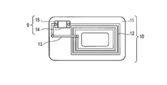
- FIG. 2 is a plan view showing an example of an IC inlet of the non-contact type information medium according to the present embodiment.
- FIG. 3 is a cross-sectional view showing an example of an IC chip of a non-contact information medium according to the present embodiment.
- FIG. 4 is a cross-sectional view showing an example of an exploded state of the porous thermoplastic base material and the IC inlet according to the present embodiment.
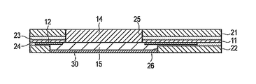
- FIG. 5 is a cross-sectional view showing an example of an assembled state of the porous thermoplastic base material, the IC inlet, and the sealing resin layer according to the present embodiment.
- FIG. 1 is a cross-sectional view showing an example of a non-contact information medium according to the present embodiment.
- FIG. 2 is a plan view showing an example of an IC inlet of the non-contact type information medium according to the present embodiment.
- FIG. 3 is a
- FIG. 6 is a cross-sectional view showing an example of a booklet attached to a non-contact type information medium according to the present embodiment.
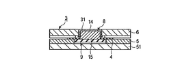
- FIG. 7 is a cross-sectional view showing an example of a conventional non-contact type information medium provided in a cover member.
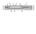
- FIG. 8 is a cross-sectional view showing an example of a non-contact type information medium according to the present embodiment provided in the cover member.
- FIG. 1 is a cross-sectional view showing an example of a non-contact type information medium 1 according to the present embodiment.
- FIG. 2 is a plan view showing an example of the IC inlet 10 of the non-contact information medium 1 according to the present embodiment.
- FIG. 3 is a cross-sectional view showing an example of the IC chip 9 of the non-contact information medium 1 according to the present embodiment.
- the non-contact type information medium 1 includes a plurality of porous thermoplastic base materials 21 and 22 and an IC inlet 10.
- the plurality of porous thermoplastic base materials 21 and 22 are used as exterior base materials.
- the porous thermoplastic base materials 21 and 22 are sheet-like.
- An opening 25 is formed in the porous thermoplastic substrate 21.
- An opening 26 is formed in the porous thermoplastic substrate 22.
- the IC inlet 10 is disposed in the openings 25 and 26 of the porous thermoplastic substrates 21 and 22 and is sandwiched between the porous thermoplastic substrates 21 and 22.
- the IC inlet 10 includes an IC chip 9 and an antenna coil 12 connected to the IC chip 9.
- the IC chip 9 includes a module unit 14 and a lead frame unit 15.
- the antenna type is the antenna coil 12 will be described, but other types of antennas are also applicable.
- the antenna coil 12 is formed on one surface of the antenna sheet base 11. On the other surface of the antenna sheet substrate 11, a wiring shape including the antenna jumper 13 and the like is provided. One end of the antenna coil 12 is connected to one of the lead frame portions 15 of the IC chip 9 via a welded portion 16. The other end of the antenna coil 12 is connected to the other end of the lead frame portion 15 via the antenna jumper 13 via the welded portion 16. Based on the antenna coil 12 and the IC chip 9, the IC inlet 10 is formed.
- the antenna coil 12 is not limited to a sheet structure, and a wound antenna structure may be used.
- the antenna coil 12 As a method of forming the antenna coil 12 on the antenna sheet substrate 11, for example, an etching method or a printed antenna method is used. In the present embodiment, it is assumed that the antenna coil 12 is manufactured using an etching method that can increase durability and reliability.
- a material of the antenna coil 12 and the antenna jumper 13 formed by the etching method for example, aluminum or copper is used.
- Aluminum is advantageous in that it is inexpensive, easy to process, and resistant to oxidation, but corrosion or dissolution may occur due to contact with the electrolyte. Copper is highly resistant to chemicals but is expensive and tends to corrode due to oxidation.
- the antenna coil 12 is manufactured by the printed antenna method, the antenna is formed by printing ink containing silver or carbon.
- a plastic film such as PET or PEN may be used as the antenna sheet substrate 11.
- a metal thin film is formed on the antenna sheet substrate 11 by plating, vapor deposition, bonding, or the like.
- Resin is printed on the antenna sheet base material 11 with metal foil obtained in this way, and an antenna coil pattern is formed.
- the antenna sheet base material 11 on which the antenna coil pattern is formed is immersed in a corrosive solution, an etching process is performed, and portions other than the antenna coil pattern on which the resin is printed are melted and removed to form an etched antenna coil. Is done.
- An antenna jumper 13 is provided on the surface opposite to the surface on which the antenna coil 12 is formed.
- the antenna jumper 13 is formed by, for example, forming a metal foil on both surfaces of the antenna sheet base material 11 in advance and providing a resin pattern on both surfaces, and performing an etching process simultaneously with the antenna coil 12, or on one side. After the antenna coil pattern is formed on the antenna jumper 13, only the antenna jumper 13 is attached.
- the IC inlet 10 may not be applied, and a method in which an antenna is directly formed on the exterior base material by winding or the like may be applied.
- an antenna is formed by heating a coated copper wire or the like while being embedded in one exterior base material, and this antenna is connected to the IC chip 9, and then the one exterior base material and the other exterior base material are connected.
- An exterior base material is bonded together.
- the antenna can be formed more easily than in the etching method, but the stability such as frequency characteristics may be inferior to the etching method, and can be used properly depending on the application.
- thermoplastic resin sheet such as PVC or PET-G
- the porous thermoplastic substrates 21 and 22 are used as the exterior substrate of the non-contact type information medium 1.
- the porous thermoplastic base materials 21 and 22 are generally marketed as resin sheets or synthetic paper imparted with printability for inkjet or offset.
- FIG. 4 is a cross-sectional view showing an example of an exploded state of the porous thermoplastic base materials 21 and 22 and the IC inlet 10 according to the present embodiment.
- thermoplastic adhesive layers 23 and 24 are previously applied to the inner portions of the two porous thermoplastic base materials 21 and 22, respectively.
- the two porous thermoplastic base materials 21 and 22 are laminated with the IC inlet 10 interposed therebetween, and are bonded by applying hot pressure.
- FIG. 5 is a cross-sectional view showing an example of an assembled state of the porous thermoplastic substrates 21 and 22, the IC inlet 10, and the sealing resin layer 30 according to the present embodiment.
- the thickness of the IC chip 9 is generally about 100 ⁇ m or more and 300 ⁇ m or less on the module part 14 side and about 100 ⁇ m or more and 300 ⁇ m or less on the lead frame part 15 side. Accordingly, when an assembled general non-contact type information medium is made to have a shape without unevenness without making a hole in the base material, the entire thickness increases, and it is necessary to mold at a high temperature and high pressure.
- the module part 14 and the lead frame part 15 of the IC chip 9 are exposed through the openings 25 and 26 of the porous thermoplastic substrates 21 and 22.
- the thickness of the antenna sheet substrate 11 is generally about 20 ⁇ m or more and 40 ⁇ m or less, and the thickness of the antenna coil 12 is about 20 ⁇ m or more and 40 ⁇ m or less. Therefore, the antenna sheet 12 is sandwiched between the porous thermoplastic substrates 21 and 22. By applying, irregularities such as antennas can be absorbed.
- thermoplastic adhesive ethylene-vinyl acetate copolymer system, ethylene-methacrylic acid copolymer system, polyester system, acrylic resin, nylon system, polyamide system, polyurethane system, polyolefin system, etc.
- thermoplastic resins can be used.
- the adhesive layers 23 and 24 have barrier performance.
- the antenna coil 12 may be protected by this barrier performance.
- a resin that forms a coating film that is particularly resistant to moisture and suppresses permeation of oxygen or chloride ions is preferably used as the thermoplastic adhesive.
- thermoplastic adhesive a resin that does not deteriorate due to heat and humidity and hardly peels off at the bonded portion is preferable.
- two or more types of resins may be mixed as an adhesive, or two or more layers of resins may be applied.
- a resin that is easy to apply, hardly blocks after drying, and has high durability is suitable.
- a suitable adhesive by applying a gravure coater with a resin obtained by adding an epoxy crosslinking agent to an ethylene-methacrylic acid copolymer aqueous emulsion adhesive, or a polyolefin or acrylic adhesive. Performance can be obtained.
- polyester-based adhesives may cause hydrolysis due to humidity, and ethylene-vinyl acetate copolymer adhesives are likely to deteriorate over time, so care must be taken.
- the module part 14 and the lead frame part 15 of the IC chip 9 are exposed through the openings 25 and 26. ing. In this state, there is a concern that moisture or the like may enter from the gap between the porous thermoplastic base material 22 and the lead frame portion 15.
- the lead frame portion 15 of the IC chip 9 is often made of copper.
- the antenna coil 12 is made of aluminum, the electrolyte penetrates to the junction between the IC chip 9 and the antenna coil 12, and the antenna coil 12 is corroded. It is likely to occur. Specifically, aluminum may be dissolved in the electrolyte due to a potential difference generated between aluminum and copper.
- the electrolyte may pass through the porous thermoplastic base material 22 and contact the antenna coil 12.
- the antenna coil is the same as when the electrolyte enters from the gap between the lead frame portion 15 and the porous thermoplastic substrate 22. 12 may corrode. Therefore, in this embodiment, as shown in FIG. 5, not only is the gap between the lead frame portion 15 and the porous thermoplastic base material 22 filled with the sealing resin layer 30, but also the exposed portion of the lead frame portion 15. The whole is covered with the sealing resin layer 30 to prevent moisture from entering.
- FIG. 6 is a cross-sectional view showing an example of the non-contact information medium attached booklet 2 according to the present embodiment.
- the non-contact type information medium 1 is provided in a booklet by being sandwiched and bonded between a cover member 42 of the booklet and the inner paste paper 41.
- the inner-attached paper 41 is bonded using an adhesive layer 43 having a barrier performance.
- an aqueous emulsion adhesive is frequently used from the viewpoint of workability and environment. The reason for this is that equipment for producing a general booklet often bonds paper and paper or cloth and paper.
- the non-contact type information medium provided in the non-contact type information medium accessory booklet 2 is made using an exterior base material such as PVC or PET-G used for a general IC card, It is difficult to bond the inner sheet 41 with existing equipment and an adhesive, and there arises a problem that the rigidity is increased.
- the porous thermoplastic base materials 21 and 22 are used as exterior base materials.
- the porous thermoplastic substrates 21 and 22 have good adhesion to various types of adhesives and have few irregularities.
- a flexible non-contact information medium-attached booklet 2 can be produced. Furthermore, by mixing a curing agent with the adhesive layer 43 or selecting an appropriate resin system as the adhesive layer 43, moisture, electrolyte, oxygen, and the like are transferred to the non-contact information medium 1 side. Intrusion can be prevented.
- the porous thermoplastic substrate 22 and the cover member 42 are bonded using an adhesive layer 44 having a barrier performance.
- an adhesive layer 44 a water-based emulsion adhesive may be used in the same manner as the adhesion of the inner sheet 41.
- the adhesive layer 44 is formed, for example, together with the sealing resin layer 30 provided on the lead frame portion 15 of the IC chip 9.
- the adhesive layer 44 is formed as an adhesive layer / sealing resin layer
- the adhesive layer 44 and the sealing resin layer 30 are manufactured in one step.
- a dry-curing adhesive such as a water-based emulsion adhesive may not be suitable.
- the amount of the adhesive used is increased.
- the volume of the sheet becomes large, a dent is formed on the outside of the cover member 42, and the appearance is deteriorated.
- an adhesive having a small volume change is used for the adhesive layer 44 and the sealing resin layer 30.
- the adhesive layer 44 for example, a two-component mixed epoxy adhesive, a moisture curable silicone adhesive, a one-component curable urethane adhesive, or the like can be used.
- various hot melt adhesives such as an ethylene-vinyl acetate copolymer system, an ethylene-methacrylic acid copolymer, a polyester system, a polyamide system, a polyurethane system, and a polyolefin system can be used.
- various hot melt adhesives may be used as the adhesive layer 44 with a small volume change.
- a reactive curing type hot-melt adhesive is effective in terms of durability and anti-deformation property, barrier performance against moisture and various ions.
- the non-contact type information medium 1 according to the present embodiment configured as described above can obtain high durability by covering the exposed lead frame portion 15 of the IC chip 9 with the sealing resin layer 30.
- the non-contact information medium 1 according to the present embodiment and the non-contact information medium accessory booklet 2 provided with the non-contact information medium 1 have improved durability and can suppress corrosion of the antenna due to moisture.
- the non-contact type information medium 1 and the non-contact type information medium attached booklet 2 are smooth and thin in appearance, and have excellent durability, such as an ID card, a driver's license, an electronic passport, a savings passbook, an annuity notebook, or Realize a sailor's notebook.
- the IC chip 9 and the antenna coil 12 connected to the IC chip 9 are sandwiched between at least two porous thermoplastic substrates 21 and 22. Openings 25 and 26 through which the IC chip 9 is exposed are formed in the porous thermoplastic base materials 21 and 22, respectively.
- a sealing resin layer 30 that closes the opening 26 is formed on at least the porous thermoplastic substrate 22 on the lead frame 15 side of the IC chip 9. Therefore, in the present embodiment, the sealing resin layer 30 formed in the opening 26 suppresses the intrusion of water or the electrolytic solution and prevents the IC chip 9 or the antenna coil 12 from being corroded.
- the non-contact type information medium 1 having high flexibility and good compatibility with the adhesive is produced. This feature is particularly important when the non-contact information medium accessory booklet 2 is produced.
- the sealing resin layer 30 may have a barrier property against the electrolytic solution or various ions.
- the sealing resin layer 30 may have a barrier property against the electrolytic solution or various ions.
- a layer having a barrier property against the electrolytic solution and various ions may be formed on the porous thermoplastic base materials 22 and 23. Thereby, the antenna coil 12 can be protected.
- the antenna coil 12 may be an aluminum antenna formed by an etching method. Thereby, it is possible to obtain superior radio wave characteristics, frequency stability, and oxidation resistance, for example, compared to a copper wound antenna, and durability against corrosion when the electrolytic solution penetrates due to the action of the sealing resin layer 30. Can be secured.
- the non-contact type information medium 1 may be bonded to the cover member 42 of the non-contact type information medium attached booklet 2 with the same material as the sealing resin layer 30. In this way, by using the adhesive layer 44 for bonding to the cover member 42 also as the sealing resin layer 30, the non-contact information medium accessory booklet 2 having excellent durability can be easily produced. .
- the sealing resin layer 30 may be a reactive hot melt adhesive.
- the sealing resin layer 30 may be formed so as to cover the opening 25 on the module unit 14 side.
- the sealing resin layer 30 formed on the module unit 14 side may be formed integrally with the adhesive layer 43.
- FIG. 7 is a cross-sectional view showing an example of a conventional non-contact information medium described in International Publication Number WO2011 / 024844.
- the conventional non-contact information medium 3 includes an aluminum antenna 4.
- an electrolyte such as salt water
- corrosion may occur due to a battery effect between the copper of the lead frame portion 15 and the aluminum antenna 4. Therefore, in the conventional non-contact type information medium 3, liquid is prevented from entering by providing a barrier layer on the exterior base material 5 in contact with the aluminum antenna 4.
- the IC inlet 8 including the IC chip 7 and the aluminum antenna 4 is exposed.
- the IC inlet 8 and the cover member (cover cloth) 51 are bonded together with an adhesive.
- the adhesive does not form a smooth film, and the liquid easily penetrates into the non-contact type information medium 3.
- a protective film 31 or a protective tape is affixed on the module part 14 in order to protect the IC chip 9 from external impacts.
- the physical loads required for protecting the IC chip 9 are mainly a stamp test and a scratch test using a ballpoint pen. Since the protective film 31 disperses the pressure, the impact resistance performance is improved.
- the flexibility of the IC chip 9 is reduced by attaching the protective film 31 to the IC chip 9. Moreover, the load at the time of bending may concentrate on the IC chip 9, and the non-contact information medium 3 may be damaged.
- the protective film 31 is made substantially the same size as the IC chip 9 and is pasted on the IC chip 9 with high accuracy, thereby maintaining the flexibility and ensuring the protection function. ing.
- FIG. 8 is a cross-sectional view showing an example of the non-contact type information medium 1 according to the present embodiment provided in the cover member 42.
- the lead frame portion 15 of the IC chip 9 that is not covered (ie, exposed) with the porous thermoplastic base material 22 is sealed with the sealing resin. Sealing with layer 30 prevents the antenna coil 12 from corroding.
- the opening resin 26 on the lead frame 15 side is filled with the sealing resin layer 30.
- the sealing resin layer 30 is formed between the lead frame portion 15 and the adhesive layer 44. Thereby, it is possible to prevent the liquid from entering the inside of the non-contact type information medium 1.
- the adhesive layer 44 a hot melt adhesive resistant to moisture may be used. Therefore, the hot melt adhesive can also be used as the sealing resin layer 30.
- the adhesive layer 44 is also used as the sealing resin layer 30, the adhesive layer 44 having an increased film thickness is formed on the lead frame portion 15 side of the non-contact type information medium 1, and the cover layer is used thereon.
- the lead frame 15 is sealed by attaching the member 42 and applying pressure.
- the adhesive used to bond the cloth is an aqueous emulsion adhesive (for example, vinyl acetate).
- a water-based emulsion adhesive has low water resistance and a low function as a sealing resin. Therefore, as in this embodiment, the significance of using a hot melt adhesive is great.
- the sealing resin layer 30 is formed on the lower side (lead frame portion 15 side) of the module portion 14 of the IC chip 9, the cushion effect can be enhanced and the impact resistance can be improved. Can do. As the sealing resin layer 30 and the adhesive layer 44 are softer, cushioning properties can be improved. By selecting a resin having both water resistance and flexibility as the sealing resin layer 30 and the adhesive layer 44, barrier performance and impact resistance performance can be improved.
- the barrier layer of the base material and the protective film 31 can be deleted, the base material coating process can be simplified, and the production cost can be reduced.
- the thickness of the sealing resin layer 30 is set to be a porous heat. It corresponds to a step between the plastic substrate 22 and the lead frame portion 15 and is, for example, approximately 1 ⁇ m or more and 20 ⁇ m or less.
- barrier performance can be obtained if the thickness of the adhesive layer 44 is about 10 ⁇ m or more, while the thickness of the adhesive layer 44 is about 100 ⁇ m. Exceeding this is undesirable because the flexibility of the entire product is reduced.
- the coating amount of the adhesive layer 44 is appropriately determined in accordance with the thickness standard of the entire product.
- the sealing resin layer 30 has physical properties that it can be bonded to, for example, the lead frame portion 15 and the porous thermoplastic base material 22, does not transmit moisture, is resistant to chemicals, and has high shock absorption and flexibility for bending.
- a hot melt adhesive is preferable.
- thermoplastic adhesive a solvent-based adhesive mainly composed of EVA is used.
- the antenna coil 12 and the antenna jumper 13 are joined by laser welding, and both ends of the antenna coil 12 are welded to the lead frame portion 15 of the IC chip 9.
- the outer periphery of the antenna coil 12 is 80 mm ⁇ 48 mm, and the inner periphery is 67 mm ⁇ 37 mm.
- the inside of the antenna coil 12 is removed by punching with a size of 65 mm ⁇ 35 mm.
- an outline 2 mm away from the outer periphery of the antenna coil 12 and the IC chip 9 is secured, and the antenna sheet substrate 11 outside the outline is punched and removed to produce the IC inlet 10.
- the thickness of the module portion 14 of the IC chip 9 is approximately 200 ⁇ m, and the thickness of the lead frame portion 15 is approximately 200 ⁇ m.
- a porous polyolefin sheet having a thickness of approximately 220 ⁇ m is prepared as the porous thermoplastic substrates 21 and 22, and a polyolefin adhesive is applied to approximately 10 ⁇ m on one side of each of the porous thermoplastic substrates 21 and 22. After these sheets are dried, the sheets are cut into approximately 150 mm ⁇ 200 mm sheets, and openings 25 and 26 are formed in portions overlapping the IC chip 9, respectively.
- the IC inlet 10 is overlaid on the adhesive surface side of one porous thermoplastic base material 22 prepared as described above, and the other porous thermoplastic base material 21 also has an adhesive surface on the IC inlet 10. They are stacked by being stacked inside.
- the laminated sheets are bonded by being sandwiched between two SUS plates and heated and pressurized.
- the bonded laminated sheet is appropriately processed between a heating part temperature of 100 ° C. to 200 ° C., a pressure of 10 Kgf / cm 2 to 50 Kgf / cm 2 , and a processing time of 10 seconds to 60 seconds.
- a contact information medium 1 is produced.
- a high quality paper is pasted on the surface of the IC chip 9 of the manufactured non-contact type information medium 1 on the module part 14 side using a vinyl acetate aqueous adhesive mixed with an epoxy curing agent. Further, a cover member 42 is bonded to the surface on the lead frame side of the IC chip 9 of the non-contact type information medium using a reactive urethane hot melt adhesive. Thereby, the non-contact information medium attached booklet 2 is produced.
- the reactive urethane hot melt adhesive is appropriately applied at a coating amount between approximately 10 ⁇ m and 100 ⁇ m. Thereby, the reactive urethane hot melt adhesive completely covers the lead frame portion 15 of the IC chip 9, and the adhesive layer 44 and the sealing resin layer 30 are formed.
- the antenna did not dissolve.
- the sealing resin layer 30 provided in the lead frame portion 15 prevents salt water from entering, and confirms the effectiveness of the contactless information 1 according to the present embodiment and examples.
- the present invention is applicable to a non-contact type information medium that includes an antenna coil and an IC chip and can record information on the IC chip in a non-contact manner, and a booklet including the non-contact type information medium.
Abstract
A contactless information medium according to the present embodiment comprises: an IC chip; an antenna connected to the IC chip; and a plurality of porous thermoplastic substrates which sandwich the IC chip and the antenna. Aperture parts which expose the IC chip are formed in each of the plurality of porous thermoplastic substrates. The contactless information medium further comprises a sealing resin layer which seals the aperture part on at least a lead frame side of the IC chip.
Description
本発明は、アンテナとIC(集積回路)チップとを備え、非接触でICチップに情報を記録させることが可能な非接触型情報媒体及びこの非接触型情報媒体を備えた冊子に関する。
The present invention relates to a non-contact type information medium that includes an antenna and an IC (integrated circuit) chip and can record information on the IC chip in a non-contact manner, and a booklet including the non-contact type information medium.
近年、非接触型情報媒体の普及は著しい。特に、非接触ICカード又は非接触ICタグを用いたシステムは、各方面で利用されている。
In recent years, the spread of non-contact information media is remarkable. In particular, systems using non-contact IC cards or non-contact IC tags are used in various directions.
また、例えばパスポート又は預貯金通帳などの冊子形状の情報媒体に、非接触型情報媒体を付加した非接触型情報媒体付属冊子が開発されている。このような非接触型情報媒体付属冊子に利用されている非接触型情報媒体は、アンテナとこのアンテナに接続される非接触ICチップとを含むICインレットを、外装基材で挟み込んだ構成を持つ。非接触型情報媒体付属冊子は、この非接触型情報媒体を、カバークロスなどと呼ばれる表紙用部材に貼り合わせ、さらに、内貼り用紙又は本文用紙などのような冊子を貼り付け、装丁される。このような非接触型情報媒体付属冊子は、通常の冊子のようにデータの印字又はVISAスタンプの付与が可能であり、電子データの記録も可能であるという特徴を持つ。
Also, for example, a booklet attached to a non-contact type information medium in which a non-contact type information medium is added to a booklet-shaped information medium such as a passport or a savings passbook has been developed. The non-contact type information medium used for such a non-contact type information medium-attached booklet has a configuration in which an IC inlet including an antenna and a non-contact IC chip connected to the antenna is sandwiched between outer packaging substrates. . The booklet attached to the non-contact type information medium is bound by sticking the non-contact type information medium to a cover member called a cover cloth or the like, and further attaching a booklet such as an inner sheet or a body sheet. Such a booklet attached to a non-contact type information medium has a feature that data can be printed or a VISA stamp can be added like an ordinary booklet, and electronic data can be recorded.
このように裏表紙の内部に非接触型情報媒体を備えた冊子は、例えば文献1(特開2002-042068号公報)に開示されている。この文献1に記載されている非接触型情報媒体は、第1の基材、第2の基材、アンテナコイル、ICチップ及び接着剤層を備える。第2の基材には、所定の広さの開口部が設けられている。第2の基材が第1の基材に接着されることにより、開口部が凹部になる。そして、この凹部内にアンテナコイルとこのアンテナコイルに接続されたICチップとが配置される。第1の基材に接着剤層が形成される。文献1の非接触型情報媒体は、接着剤層によって冊子の裏表紙の内面に貼付される。
A booklet having a non-contact type information medium inside the back cover as described above is disclosed in, for example, Document 1 (Japanese Patent Laid-Open No. 2002-04068). The non-contact information medium described in Document 1 includes a first base material, a second base material, an antenna coil, an IC chip, and an adhesive layer. The second base is provided with an opening having a predetermined width. By bonding the second base material to the first base material, the opening becomes a recess. An antenna coil and an IC chip connected to the antenna coil are disposed in the recess. An adhesive layer is formed on the first substrate. The non-contact type information medium of Document 1 is attached to the inner surface of the back cover of a booklet with an adhesive layer.
また、流通しているクレジットカード又はICカードにおいても、非接触型情報媒体が備えられる場合がある。
Also, there are cases where a non-contact type information medium is provided in a distributed credit card or IC card.
非接触型情報媒は、例えばPVC又はPET-Gなどのシートのような熱可塑性の基材の間に、IC及びアンテナ等を挟みこみ、強い熱圧をかけ、基材を流動させて平滑することで作製される。
A non-contact type information medium is smoothed by sandwiching an IC and an antenna between thermoplastic substrates such as sheets of PVC or PET-G, applying a strong heat pressure, and flowing the substrate. It is produced by.
非接触型情報媒体を冊子の表又は裏の表紙と内貼り用紙の間に接着することで、非接触型情報媒体付属冊子が作製される。
• A non-contact type information medium attached booklet is produced by adhering the non-contact type information medium between the front or back cover of the booklet and the inner sheet.
このような非接触型情報媒体は、PVC又はPET-GなどのシートでICチップ及びアンテナが密閉されるため、水分又は薬品に対して耐久性が高い。しかし、この非接触型情報媒体がそのまま冊子に接着され使用される場合、剛度が高くなって表紙が開きにくくなる場合があり、基材と内貼り用紙との接着が困難な場合がある。これらの問題を解決する手法の一つとして、これらPVC又はPET-Gなどのシートの代わりに、熱可塑性で基材中に空隙を有する多孔質のシートを利用してもよい。
Such a non-contact type information medium has high durability against moisture or chemicals because the IC chip and the antenna are sealed with a sheet of PVC or PET-G. However, when this non-contact type information medium is directly adhered to a booklet and used, the rigidity may be increased and the cover may be difficult to open, and it may be difficult to bond the base material to the inner sheet. As one method for solving these problems, a porous sheet having a void in the substrate may be used instead of the sheet such as PVC or PET-G.
この多孔質熱可塑性シートは、樹脂を発泡させることによって作製され、一般に材料が柔らかく剛度が低い。また、多孔質熱可塑性シートは、空隙を持つことにより様々な接着剤が容易に浸透し、内貼り用紙との接着性が高い。さらに、多孔質熱可塑性シートは、適度な圧力をかけることで凹凸を吸収することが可能である。このような多孔質熱可塑性シートが基材として使用される場合、多孔質熱可塑性シート自体を熱融着によって接着すること、熱可塑性の接着剤を多孔質熱可塑性シートに塗布した後で熱ラミネート方式により接着すること、一般に使われるような水系又は溶剤系の乾燥固化型の接着剤を多孔質熱可塑性シートに塗布して接着すること、が可能である。
This porous thermoplastic sheet is produced by foaming a resin and generally has a soft material and low rigidity. In addition, since the porous thermoplastic sheet has voids, various adhesives can easily permeate and have high adhesiveness with the inner sheet. Furthermore, the porous thermoplastic sheet can absorb irregularities by applying an appropriate pressure. When such a porous thermoplastic sheet is used as a base material, the porous thermoplastic sheet itself is bonded by thermal fusion, and after the thermoplastic adhesive is applied to the porous thermoplastic sheet, thermal lamination is performed. It is possible to adhere by a method, or to apply and adhere a commonly used water-based or solvent-based dry-solidified adhesive to a porous thermoplastic sheet.
ただし、このような多孔質熱可塑性シートに接着剤を塗布して貼りあわせる方式を適用した場合、圧力をかけても凹凸が吸収しきれない場合がある。仮に、凹凸を吸収できるぐらいの熱圧がかけられると、樹脂が溶融して流動し、多孔質の利点が低下する場合がある。
However, when a method of applying and bonding an adhesive to such a porous thermoplastic sheet is applied, unevenness may not be absorbed even when pressure is applied. If a hot pressure that can absorb unevenness is applied, the resin may melt and flow, and the advantage of the porousness may be reduced.
一般に、アンテナの厚みは、20μmから50μm程度であり、この程度の厚みであれば基材の厚みによって吸収できる。しかしながら、ICチップの厚みは、300μm以上の場合もあり、少なくとも基材はICチップよりも厚い必要がある。非接触型情報媒体全体の厚みを薄くするため、基材にICチップと同じ大きさの開口部が設けられ、ICチップとアンテナとが挟み込まれた非接触型情報媒体が作製される場合がある。
Generally, the thickness of the antenna is about 20 μm to 50 μm. If the thickness is about this, it can be absorbed by the thickness of the base material. However, the thickness of the IC chip may be 300 μm or more, and at least the substrate needs to be thicker than the IC chip. In order to reduce the thickness of the entire non-contact information medium, an opening having the same size as the IC chip is provided on the base material, and a non-contact information medium in which the IC chip and the antenna are sandwiched may be manufactured. .
上述のように、多孔質熱可塑性基材を用いて形成される非接触型情報媒体及び非接触型情報媒体付属冊子は、製造が容易で柔軟性に富み、他の材料との接着性もよいが、しかしながら、水分又は薬品に対する耐久性が劣る。
As described above, the non-contact type information medium and the non-contact type information medium-attached booklet formed using the porous thermoplastic base material are easy to manufacture, rich in flexibility, and have good adhesion to other materials. However, the durability against moisture or chemicals is poor.
この問題を解決するために、多孔質熱可塑性基材にバリア層を設ける方式、又は、接着層にバリア性能を持たせる方式が提案されている。しかしながら、ICチップに対応する開口部が設けられる場合には、その開口部から水分又は薬品が浸入し、耐久性が不十分になる場合がある。
In order to solve this problem, a method of providing a barrier layer on a porous thermoplastic base material, or a method of giving a barrier performance to an adhesive layer has been proposed. However, when an opening corresponding to the IC chip is provided, moisture or chemical may enter from the opening and durability may be insufficient.
本発明は、上記実情を鑑みてなされたものであり、耐水性又は耐薬品性を有し、ICチップ開口部を備えた非接触型情報媒体及びこの非接触型情報媒体を備えた非接触型情報媒体付属冊子を提供することを目的とする。
The present invention has been made in view of the above circumstances, has water resistance or chemical resistance, and has a non-contact type information medium having an IC chip opening and a non-contact type medium having the non-contact type information medium. The purpose is to provide an information media booklet.
第1の態様に係る非接触型情報媒体は、ICチップと、ICチップに接続されたアンテナと、ICチップとアンテナとを挟装する複数の多孔質熱可塑性基材とを備える。ICチップを露出させる開口部が、複数の多孔質熱可塑性基材のそれぞれに形成されている。非接触型情報媒体は、少なくともICチップのリードフレーム側の開口部を閉塞する封止樹脂層をさらに備える。
The non-contact information medium according to the first aspect includes an IC chip, an antenna connected to the IC chip, and a plurality of porous thermoplastic substrates that sandwich the IC chip and the antenna. An opening for exposing the IC chip is formed in each of the plurality of porous thermoplastic substrates. The non-contact type information medium further includes a sealing resin layer that closes at least the opening on the lead frame side of the IC chip.
第1の態様において、封止樹脂層は、電解液又は各種イオンに対してバリア性を持つとしてもよい。第1の態様において、封止樹脂層は、反応型ホットメルト接着剤としてもよい。第1の態様において、複数の多孔質熱可塑性基材の少なくとも一方の上に、電解液又は各種イオンに対してバリア性を持つ層をさらに備えてもよい。第1の態様において、アンテナは、エッチング方式で形成されたアルミニウムアンテナとしてもよい。
In the first aspect, the sealing resin layer may have a barrier property against the electrolytic solution or various ions. In the first aspect, the sealing resin layer may be a reactive hot melt adhesive. In the first aspect, a layer having a barrier property against the electrolytic solution or various ions may be further provided on at least one of the plurality of porous thermoplastic substrates. In the first aspect, the antenna may be an aluminum antenna formed by an etching method.
第2の態様に係る非接触型情報媒体付属冊子は、第1の態様に係る非接触型情報媒体を備える。非接触型情報媒体は、封止樹脂層と同じ材料の接着剤層により非接触型情報媒体を表紙用部材に接着することにより、非接触型情報媒体を冊子に備える。
The non-contact information medium attached booklet according to the second aspect includes the non-contact information medium according to the first aspect. The non-contact type information medium is provided with a non-contact type information medium in a booklet by adhering the non-contact type information medium to the cover member with an adhesive layer made of the same material as the sealing resin layer.
本発明の態様においては、耐水性又は耐薬品性を有し、ICチップ開口部を備えた非接触型情報媒体及びこの非接触型情報媒体を備えた非接触型情報媒体付属冊子を提供することができる。
In an aspect of the present invention, there is provided a non-contact type information medium having water resistance or chemical resistance and having an IC chip opening, and a non-contact type information medium accessory booklet provided with this non-contact type information medium. Can do.
以下、本実施形態に係る非接触型情報媒体及び非接触型情報媒体付属冊子について、図面を参照して詳細に説明する。
Hereinafter, the non-contact type information medium and the non-contact type information medium attached booklet according to the present embodiment will be described in detail with reference to the drawings.
図1は、本実施形態に係る非接触型情報媒体1の一例を示す断面図である。
FIG. 1 is a cross-sectional view showing an example of a non-contact type information medium 1 according to the present embodiment.
図2は、本実施形態に係る非接触型情報媒体1のICインレット10の一例を示す平面図である。
FIG. 2 is a plan view showing an example of the IC inlet 10 of the non-contact information medium 1 according to the present embodiment.
図3は、本実施形態に係る非接触型情報媒体1のICチップ9の一例を示す断面図である。
FIG. 3 is a cross-sectional view showing an example of the IC chip 9 of the non-contact information medium 1 according to the present embodiment.
非接触型情報媒体1は、複数の多孔質熱可塑性基材21,22とICインレット10とを備える。複数の多孔質熱可塑性基材21,22は、外装基材として用いられる。多孔質熱可塑性基材21,22は、シート状である。多孔質熱可塑性基材21には開口部25が形成されている。多孔質熱可塑性基材22には、開口部26が形成されている。
The non-contact type information medium 1 includes a plurality of porous thermoplastic base materials 21 and 22 and an IC inlet 10. The plurality of porous thermoplastic base materials 21 and 22 are used as exterior base materials. The porous thermoplastic base materials 21 and 22 are sheet-like. An opening 25 is formed in the porous thermoplastic substrate 21. An opening 26 is formed in the porous thermoplastic substrate 22.
ICインレット10は、多孔質熱可塑性基材21,22の開口部25,26に配置され、かつ、多孔質熱可塑性基材21,22で挟装される。
The IC inlet 10 is disposed in the openings 25 and 26 of the porous thermoplastic substrates 21 and 22 and is sandwiched between the porous thermoplastic substrates 21 and 22.
ICインレット10は、ICチップ9とこのICチップ9に接続されるアンテナコイル12とを備える。ICチップ9は、モジュール部14と、リードフレーム部15とを備える。本実施形態においては、アンテナの種類がアンテナコイル12の場合について説明するが、他の種類のアンテナであっても適用可能である。
The IC inlet 10 includes an IC chip 9 and an antenna coil 12 connected to the IC chip 9. The IC chip 9 includes a module unit 14 and a lead frame unit 15. In the present embodiment, the case where the antenna type is the antenna coil 12 will be described, but other types of antennas are also applicable.
アンテナコイル12は、アンテナシート基材11の一方面に形成される。アンテナシート基材11の他方面には、アンテナジャンパー13などを含む配線形状が備えられる。アンテナコイル12の一方端は、ICチップ9のリードフレーム部15の一方に溶接部分16を介して接続される。アンテナコイル12の他方端は、アンテナジャンパー13を介してリードフレーム部15の他方に溶接部分16を介して接続される。このようなアンテナコイル12とICチップ9とに基づいて、ICインレット10が形成される。アンテナコイル12としては、シート構造に限定されず、巻き線アンテナ構造が用いられてもよい。
The antenna coil 12 is formed on one surface of the antenna sheet base 11. On the other surface of the antenna sheet substrate 11, a wiring shape including the antenna jumper 13 and the like is provided. One end of the antenna coil 12 is connected to one of the lead frame portions 15 of the IC chip 9 via a welded portion 16. The other end of the antenna coil 12 is connected to the other end of the lead frame portion 15 via the antenna jumper 13 via the welded portion 16. Based on the antenna coil 12 and the IC chip 9, the IC inlet 10 is formed. The antenna coil 12 is not limited to a sheet structure, and a wound antenna structure may be used.
アンテナコイル12をアンテナシート基材11に形成する手法としては、例えば、エッチング方式又は印刷アンテナ方式などが用いられる。本実施形態においては、耐久性と信頼性を高くすることができるエッチング方式を用いてアンテナコイル12が製造されるとする。エッチング方式によって形成されるアンテナコイル12及びアンテナジャンパー13の素材としては、例えば、アルミニウム、銅が用いられる。アルミニウムは、価格が安く、加工しやすく、酸化に強いという利点があるが、電解質と接触することにより腐食又は溶解が生じる場合がある。銅は薬品に対する耐久性は高いが、価格が高く、酸化することにより腐食が進行しやすい傾向がある。印刷アンテナ方式によってアンテナコイル12が製造される場合には、銀又はカーボンを含有するインキを印刷することによってアンテナが形成される。
As a method of forming the antenna coil 12 on the antenna sheet substrate 11, for example, an etching method or a printed antenna method is used. In the present embodiment, it is assumed that the antenna coil 12 is manufactured using an etching method that can increase durability and reliability. As a material of the antenna coil 12 and the antenna jumper 13 formed by the etching method, for example, aluminum or copper is used. Aluminum is advantageous in that it is inexpensive, easy to process, and resistant to oxidation, but corrosion or dissolution may occur due to contact with the electrolyte. Copper is highly resistant to chemicals but is expensive and tends to corrode due to oxidation. When the antenna coil 12 is manufactured by the printed antenna method, the antenna is formed by printing ink containing silver or carbon.
エッチングアンテナを例として説明すると、アンテナシート基材11としては、PET又はPEN等のようなプラスティックフィルムが用いられてもよい。このアンテナシート基材11の上に、メッキ法、蒸着法、貼りあわせ法などにより、金属の薄膜が形成される。このようにして得られた金属箔付きのアンテナシート基材11の上に樹脂が印刷され、アンテナコイルパターンが形成される。次に、アンテナコイルパターンが形成されたアンテナシート基材11が腐食液に漬けられ、エッチング処理が実行され、樹脂の印刷されたアンテナコイルパターンを除く部分が溶けて除去され、エッチングアンテナコイルが形成される。また、アンテナコイル12の形成された面の反対面には、アンテナジャンパー13が備えられる。このアンテナジャンパー13は、例えば、予めアンテナシート基材11の両面に対して金属箔を形成し、両面に樹脂のパターンを設けることにより、アンテナコイル12と同時にエッチング処理を行うことで、又は、片面にアンテナコイルパターンを形成した後にアンテナジャンパー13のみを貼り付けることで、形成される。
When an etching antenna is described as an example, a plastic film such as PET or PEN may be used as the antenna sheet substrate 11. A metal thin film is formed on the antenna sheet substrate 11 by plating, vapor deposition, bonding, or the like. Resin is printed on the antenna sheet base material 11 with metal foil obtained in this way, and an antenna coil pattern is formed. Next, the antenna sheet base material 11 on which the antenna coil pattern is formed is immersed in a corrosive solution, an etching process is performed, and portions other than the antenna coil pattern on which the resin is printed are melted and removed to form an etched antenna coil. Is done. An antenna jumper 13 is provided on the surface opposite to the surface on which the antenna coil 12 is formed. The antenna jumper 13 is formed by, for example, forming a metal foil on both surfaces of the antenna sheet base material 11 in advance and providing a resin pattern on both surfaces, and performing an etching process simultaneously with the antenna coil 12, or on one side. After the antenna coil pattern is formed on the antenna jumper 13, only the antenna jumper 13 is attached.
ICインレット10が適用されず、巻き線加工などによって外装基材に直接アンテナが形成される方法が適用されてもよい。この方式では、被覆された銅線などを加熱しながら一方の外装基材に埋め込むようにして、アンテナが形成され、このアンテナがICチップ9に接続され、その後、一方の外装基材と他方の外装基材とが貼り合わされる。この方式では、エッチング方式よりも簡易にアンテナを形成することが出来る反面、周波数特性などの安定性ではエッチング方式に劣る場合があり、用途によって使い分けられる。
The IC inlet 10 may not be applied, and a method in which an antenna is directly formed on the exterior base material by winding or the like may be applied. In this method, an antenna is formed by heating a coated copper wire or the like while being embedded in one exterior base material, and this antenna is connected to the IC chip 9, and then the one exterior base material and the other exterior base material are connected. An exterior base material is bonded together. In this method, the antenna can be formed more easily than in the etching method, but the stability such as frequency characteristics may be inferior to the etching method, and can be used properly depending on the application.
一般的な非接触型情報媒体の外装基材としては、例えばPVC又はPET-Gのような熱可塑性樹脂シートが用いられることが一般的である。しかしながら、本実施形態においては、非接触型情報媒体1の外装基材として多孔質熱可塑性基材21,22が使用される。多孔質熱可塑性基材21,22は、一般にインクジェット又はオフセットなどに対する印刷適性を付与した樹脂シート又は合成紙として市販されている。非接触型情報媒体1の外装基材として、このような多孔質熱可塑性基材21,22を使用することで柔軟性のある非接触型情報媒体1を形成することができる。また、多孔質熱可塑性基材21,22を使用することで、非接触型情報媒体1を冊子など別の媒体と貼り合わせる場合に、接着剤と良好な密着性を得ることができ、優れた加工性を得ることができる。
As a general non-contact information medium exterior base material, for example, a thermoplastic resin sheet such as PVC or PET-G is generally used. However, in this embodiment, the porous thermoplastic substrates 21 and 22 are used as the exterior substrate of the non-contact type information medium 1. The porous thermoplastic base materials 21 and 22 are generally marketed as resin sheets or synthetic paper imparted with printability for inkjet or offset. By using such porous thermoplastic base materials 21 and 22 as the exterior base material of the non-contact type information medium 1, the flexible non-contact type information medium 1 can be formed. Further, by using the porous thermoplastic base materials 21 and 22, when the non-contact type information medium 1 is bonded to another medium such as a booklet, it is possible to obtain good adhesiveness with the adhesive, and it is excellent. Workability can be obtained.
図4は、本実施形態に係る多孔質熱可塑性基材21,22とICインレット10との分解状態の一例を示す断面図である。
FIG. 4 is a cross-sectional view showing an example of an exploded state of the porous thermoplastic base materials 21 and 22 and the IC inlet 10 according to the present embodiment.
2枚の多孔質熱可塑性基材21,22のそれぞれの内側部分には、あらかじめ熱可塑性の接着剤層23,24がそれぞれ塗布されている。2枚の多孔質熱可塑性基材21,22は、ICインレット10を挟んで積層され、熱圧をかけることで接着される。
The thermoplastic adhesive layers 23 and 24 are previously applied to the inner portions of the two porous thermoplastic base materials 21 and 22, respectively. The two porous thermoplastic base materials 21 and 22 are laminated with the IC inlet 10 interposed therebetween, and are bonded by applying hot pressure.
図5は、本実施形態に係る多孔質熱可塑性基材21,22とICインレット10と封止樹脂層30との組立状態の一例を示す断面図である。
FIG. 5 is a cross-sectional view showing an example of an assembled state of the porous thermoplastic substrates 21 and 22, the IC inlet 10, and the sealing resin layer 30 according to the present embodiment.
組み立てられた非接触型情報媒体1において、一般的にICチップ9の厚みは、モジュール部14側がおよそ100μm以上、300μm以下、リードフレーム部15側がおよそ100μm以上、300μm以下である。したがって、組み立てられた一般的な非接触型情報媒体について、基材に穴を開けることなく凹凸のない形状にしようとすると、全体の厚みが増し、さらに、高温高圧で成型する必要がある。本実施形態においては、ICチップ9の部分で段差のない平坦性を持ち、かつ、なるべく薄い非接触型情報媒体1を得るために、多孔質熱可塑性基材21,22に、それぞれ貫通する開口部25,26が形成される。この場合、接着された非接触型情報媒体1は、ICチップ9のモジュール部14及びリードフレーム部15が、多孔質熱可塑性基材21,22の開口部25,26を通して露出される。なお、アンテナシート基材11の厚みは一般におよそ20μm以上、40μm以下であり、アンテナコイル12の厚みはおよそ20μm以上、40μm以下であるため、多孔質熱可塑性基材21,22で挟んで熱圧をかけることでアンテナ等の凹凸は吸収することができる。
In the assembled non-contact type information medium 1, the thickness of the IC chip 9 is generally about 100 μm or more and 300 μm or less on the module part 14 side and about 100 μm or more and 300 μm or less on the lead frame part 15 side. Accordingly, when an assembled general non-contact type information medium is made to have a shape without unevenness without making a hole in the base material, the entire thickness increases, and it is necessary to mold at a high temperature and high pressure. In the present embodiment, in order to obtain a non-contact type information medium 1 having flatness with no step at the IC chip 9 portion and as thin as possible, the openings penetrating the porous thermoplastic substrates 21 and 22 respectively. Portions 25 and 26 are formed. In this case, in the bonded non-contact information medium 1, the module part 14 and the lead frame part 15 of the IC chip 9 are exposed through the openings 25 and 26 of the porous thermoplastic substrates 21 and 22. The thickness of the antenna sheet substrate 11 is generally about 20 μm or more and 40 μm or less, and the thickness of the antenna coil 12 is about 20 μm or more and 40 μm or less. Therefore, the antenna sheet 12 is sandwiched between the porous thermoplastic substrates 21 and 22. By applying, irregularities such as antennas can be absorbed.
本実施形態において、熱可塑性の接着剤として、エチレン-酢酸ビニル共重合体系、エチレン-メタクリル酸共重合体系、ポリエステル系、アクリル系樹脂、ナイロン系、ポリアミド系、ポリウレタン系、ポリオレフィン系など、一般的な各種熱可塑性の樹脂が使用可能である。本実施形態においては、多孔質熱可塑性基材21,22を水分、電解質、又は、酸素などが透過し、アンテナコイル12が劣化することを抑制するため、接着剤層23,24にバリア性能を付与し、このバリア性能によりアンテナコイル12を保護してもよい。上記の樹脂のうち、特に水分に強く、酸素又は塩化物イオンの透過を抑制するような塗膜を形成する樹脂が、熱可塑性の接着剤として用いられることが好ましい。また、熱可塑性の接着剤としては、熱及び湿度によって劣化することなく、かつ、接着部分に剥がれを生じにくい樹脂が好ましい。これらの性能を両立させるために、接着剤として、2種類以上の樹脂が混合されてもよく、2層以上の樹脂が塗工されてもよい。
In this embodiment, as the thermoplastic adhesive, ethylene-vinyl acetate copolymer system, ethylene-methacrylic acid copolymer system, polyester system, acrylic resin, nylon system, polyamide system, polyurethane system, polyolefin system, etc. Various thermoplastic resins can be used. In the present embodiment, in order to prevent moisture, electrolyte, oxygen, or the like from passing through the porous thermoplastic base materials 21 and 22 and the antenna coil 12 from deteriorating, the adhesive layers 23 and 24 have barrier performance. The antenna coil 12 may be protected by this barrier performance. Of the above resins, a resin that forms a coating film that is particularly resistant to moisture and suppresses permeation of oxygen or chloride ions is preferably used as the thermoplastic adhesive. Further, as the thermoplastic adhesive, a resin that does not deteriorate due to heat and humidity and hardly peels off at the bonded portion is preferable. In order to make these performances compatible, two or more types of resins may be mixed as an adhesive, or two or more layers of resins may be applied.
また、後工程及び作業性の面から、接着剤として、塗工が容易で、乾燥後のブロッキングが生じにくく、耐久性の高い樹脂が適している。例えば、エチレン-メタクリル酸共重合体系の水系エマルジョン接着剤にエポキシ系架橋剤を添加した樹脂、又は、ポリオレフィン系、アクリル系の接着剤などを、グラビアコーターで塗工するなどで、好適な接着剤の性能を得ることができる。一方、一般的に、ポリエステル系の接着剤は、湿度による加水分解を生じる可能性があり、エチレン-酢酸ビニル共重合体系接着剤は、経時劣化し易いので注意が必要である。
Also, from the standpoints of the post-process and workability, as the adhesive, a resin that is easy to apply, hardly blocks after drying, and has high durability is suitable. For example, a suitable adhesive by applying a gravure coater with a resin obtained by adding an epoxy crosslinking agent to an ethylene-methacrylic acid copolymer aqueous emulsion adhesive, or a polyolefin or acrylic adhesive. Performance can be obtained. On the other hand, in general, polyester-based adhesives may cause hydrolysis due to humidity, and ethylene-vinyl acetate copolymer adhesives are likely to deteriorate over time, so care must be taken.
多孔質熱可塑性基材21,22に形成された開口部25,26にICチップ9が備えられた場合、開口部25,26を通してICチップ9のモジュール部14とリードフレーム部15とが露出されている。この状態では、多孔質熱可塑性基材22とリードフレーム部15との隙間から、水分などが浸入することが懸念される。ICチップ9のリードフレーム部15は、銅が多く用いられるが、仮にアンテナコイル12がアルミニウムである場合、電解質がICチップ9とアンテナコイル12との接合部まで浸入し、アンテナコイル12の腐食が発生しやすくなる可能性がある。具体的には、アルミニウムと銅との間に生じる電位差によりアルミニウムが電解質に溶解してしまう可能性がある。また、仮にリードフレーム部15と多孔質熱可塑性基材22との隙間から電解質が浸入しなくても、電解質が多孔質熱可塑性基材22を透過してアンテナコイル12に接触する場合がある。この場合、露出しているリードフレーム部15とアンテナコイル12との間で通電すると、リードフレーム部15と多孔質熱可塑性基材22との隙間から電解質が浸入した場合と同じように、アンテナコイル12が腐食する可能性がある。このため、本実施形態においては、図5に示すように、リードフレーム部15と多孔質熱可塑性基材22との隙間を封止樹脂層30で埋めるだけでなく、リードフレーム部15の露出部全体を封止樹脂層30で覆い、水分の浸入を防ぐ。
When the IC chip 9 is provided in the openings 25 and 26 formed in the porous thermoplastic base materials 21 and 22, the module part 14 and the lead frame part 15 of the IC chip 9 are exposed through the openings 25 and 26. ing. In this state, there is a concern that moisture or the like may enter from the gap between the porous thermoplastic base material 22 and the lead frame portion 15. The lead frame portion 15 of the IC chip 9 is often made of copper. However, if the antenna coil 12 is made of aluminum, the electrolyte penetrates to the junction between the IC chip 9 and the antenna coil 12, and the antenna coil 12 is corroded. It is likely to occur. Specifically, aluminum may be dissolved in the electrolyte due to a potential difference generated between aluminum and copper. Even if the electrolyte does not enter from the gap between the lead frame portion 15 and the porous thermoplastic base material 22, the electrolyte may pass through the porous thermoplastic base material 22 and contact the antenna coil 12. In this case, when the current is passed between the exposed lead frame portion 15 and the antenna coil 12, the antenna coil is the same as when the electrolyte enters from the gap between the lead frame portion 15 and the porous thermoplastic substrate 22. 12 may corrode. Therefore, in this embodiment, as shown in FIG. 5, not only is the gap between the lead frame portion 15 and the porous thermoplastic base material 22 filled with the sealing resin layer 30, but also the exposed portion of the lead frame portion 15. The whole is covered with the sealing resin layer 30 to prevent moisture from entering.
電解質による腐食の問題は、次のような実験で確認される。アルミニウムのアンテナのみを食塩水に浸漬した場合には1時間程度でも腐食は発生しない。しかしながら、このアルミニウムのアンテナに銅の金属片を溶接し、食塩水に浸けると、数分でアルミニウム部分の溶解が生じる。さらに、この銅の部分を完全に樹脂で覆ってしまった上で食塩水に浸漬すると、樹脂の種類にもよるが溶解するまでの時間は延びる。
The problem of corrosion due to electrolyte is confirmed by the following experiment. When only an aluminum antenna is immersed in a saline solution, corrosion does not occur even for about 1 hour. However, when a copper metal piece is welded to the aluminum antenna and immersed in a saline solution, the aluminum portion dissolves in a few minutes. Furthermore, if this copper part is completely covered with resin and then immersed in a saline solution, the time required for dissolution increases depending on the type of resin.
図6は、本実施形態に係る非接触型情報媒体付属冊子2の一例を示す断面図である。
FIG. 6 is a cross-sectional view showing an example of the non-contact information medium attached booklet 2 according to the present embodiment.
非接触型情報媒体1は、冊子の表紙用部材42と内貼り用紙41との間に挟み込んで接着されることで、冊子に備えられる。多孔質熱可塑性基材21の上には、内貼り用紙41がバリア性能を持つ接着剤層43を用いて接着される。接着剤層43としては、作業性及び環境の側面から、水系のエマルジョン接着剤が頻繁に使用される。この理由としては、一般的な冊子を製造するための設備は、紙と紙、又は、布と紙の貼り合わせを行うことが多いためである。仮に、非接触型情報媒体付属冊子2に備えられる非接触型情報媒体が、一般のICカードに使われるような外装基材、例えばPVC又はPET-Gを使用して作製された場合には、既存の設備及び接着剤で内貼り用紙41を接着することが困難であり、剛度が高くなるという問題が生じる。このような問題を解決するため、本実施形態においては、多孔質熱可塑性基材21,22が外装基材として使用される。多孔質熱可塑性基材21,22は、様々なタイプの接着剤に対して良好な密着性を持ち、かつ、凹凸が少ない。多孔質熱可塑性基材21,22を用いることにより、柔軟な非接触型情報媒体付冊子2を作製することができる。さらに、上記接着剤層43に硬化剤を混合すること、又は、接着剤層43として適切な樹脂系が選択されることによって、水分、電解質、及び、酸素などが非接触型情報媒体1側へ浸入することを防ぐことができる。
The non-contact type information medium 1 is provided in a booklet by being sandwiched and bonded between a cover member 42 of the booklet and the inner paste paper 41. On the porous thermoplastic substrate 21, the inner-attached paper 41 is bonded using an adhesive layer 43 having a barrier performance. As the adhesive layer 43, an aqueous emulsion adhesive is frequently used from the viewpoint of workability and environment. The reason for this is that equipment for producing a general booklet often bonds paper and paper or cloth and paper. If the non-contact type information medium provided in the non-contact type information medium accessory booklet 2 is made using an exterior base material such as PVC or PET-G used for a general IC card, It is difficult to bond the inner sheet 41 with existing equipment and an adhesive, and there arises a problem that the rigidity is increased. In order to solve such a problem, in this embodiment, the porous thermoplastic base materials 21 and 22 are used as exterior base materials. The porous thermoplastic substrates 21 and 22 have good adhesion to various types of adhesives and have few irregularities. By using the porous thermoplastic substrates 21 and 22, a flexible non-contact information medium-attached booklet 2 can be produced. Furthermore, by mixing a curing agent with the adhesive layer 43 or selecting an appropriate resin system as the adhesive layer 43, moisture, electrolyte, oxygen, and the like are transferred to the non-contact information medium 1 side. Intrusion can be prevented.
多孔質熱可塑性基材22と表紙用部材42とは、バリア性能を持つ接着剤層44を用いて接着される。この接着剤層44としては、内貼り用紙41の接着と同様に、水系エマルジョン接着剤が使用されてもよい。
The porous thermoplastic substrate 22 and the cover member 42 are bonded using an adhesive layer 44 having a barrier performance. As the adhesive layer 44, a water-based emulsion adhesive may be used in the same manner as the adhesion of the inner sheet 41.
この図6において、接着剤層44は、例えばICチップ9のリードフレーム部15に設けた封止樹脂層30と兼用して形成される。接着剤層44を、接着剤層兼封止樹脂層として形成することで、接着剤層44と封止樹脂層30とが一回の工程で製造される。しかしながら、このような場合には、水系エマルジョン接着剤のような乾燥硬化型の接着剤が適さない場合がある。例えば、乾燥硬化型の接着剤が使用され、非接触型情報媒体1の一部、例えばリードフレーム部15の上など、に凹部がある場合には、接着剤の使用量が多くなり、乾燥時の体積減少が大きくなり、表紙用部材42の外側に凹みが生じ、外観が悪化する場合がある。このような問題を解決するために、体積変化の少ない接着剤が、接着剤層44及び封止樹脂層30に使用されることが望ましい。接着剤層44として、例えば、2液混合型エポキシ系接着剤、湿気硬化型シリコン系接着剤、1液硬化型ウレタン系接着剤、などが使用できる。また、接着剤層44として、エチレン-酢酸ビニル共重合体系、エチレン-メタクリル酸共重合体、ポリエステル系、ポリアミド系、ポリウレタン系、ポリオレフィン系など、各種のホットメルト接着剤なども使用可能である。
In FIG. 6, the adhesive layer 44 is formed, for example, together with the sealing resin layer 30 provided on the lead frame portion 15 of the IC chip 9. By forming the adhesive layer 44 as an adhesive layer / sealing resin layer, the adhesive layer 44 and the sealing resin layer 30 are manufactured in one step. However, in such a case, a dry-curing adhesive such as a water-based emulsion adhesive may not be suitable. For example, when a dry-curing type adhesive is used and there is a recess in a part of the non-contact type information medium 1, for example, on the lead frame portion 15, the amount of the adhesive used is increased. There is a case where the volume of the sheet becomes large, a dent is formed on the outside of the cover member 42, and the appearance is deteriorated. In order to solve such a problem, it is desirable that an adhesive having a small volume change is used for the adhesive layer 44 and the sealing resin layer 30. As the adhesive layer 44, for example, a two-component mixed epoxy adhesive, a moisture curable silicone adhesive, a one-component curable urethane adhesive, or the like can be used. As the adhesive layer 44, various hot melt adhesives such as an ethylene-vinyl acetate copolymer system, an ethylene-methacrylic acid copolymer, a polyester system, a polyamide system, a polyurethane system, and a polyolefin system can be used.
上記体積変化の少ない接着剤層44として、作業性の観点から、各種ホットメルト接着剤が用いられてもよい。特に、体積変化の少ない接着剤44として、耐久性及び耐変造性、水分及び各種イオンに対するバリア性能という点において、反応硬化型のホットメルト接着剤が有効である。
From the viewpoint of workability, various hot melt adhesives may be used as the adhesive layer 44 with a small volume change. In particular, as the adhesive 44 having a small volume change, a reactive curing type hot-melt adhesive is effective in terms of durability and anti-deformation property, barrier performance against moisture and various ions.
このように構成した本実施形態に係る非接触型情報媒体1は、露出したICチップ9のリードフレーム部15を封止樹脂層30で覆ったことにより、高い耐久性を得ることができる。
The non-contact type information medium 1 according to the present embodiment configured as described above can obtain high durability by covering the exposed lead frame portion 15 of the IC chip 9 with the sealing resin layer 30.
本実施形態に係る非接触型情報媒体1及びこれを備えた非接触型情報媒体付属冊子2は、耐久性が向上し、水分によるアンテナの腐食を抑制することができる。そして、この非接触型情報媒体1及び非接触型情報媒体付属冊子2は、外観が平滑かつ薄型で、耐久性に優れた例えばIDカード、運転免許証、電子パスポート、預貯金通帳、年金手帳、又は、船員手帳などを実現する。
The non-contact information medium 1 according to the present embodiment and the non-contact information medium accessory booklet 2 provided with the non-contact information medium 1 have improved durability and can suppress corrosion of the antenna due to moisture. The non-contact type information medium 1 and the non-contact type information medium attached booklet 2 are smooth and thin in appearance, and have excellent durability, such as an ID card, a driver's license, an electronic passport, a savings passbook, an annuity notebook, or Realize a sailor's notebook.
本実施形態における効果をより具体的に説明する。
The effect in the present embodiment will be described more specifically.
本実施形態においては、ICチップ9とこのICチップ9に接続されたアンテナコイル12とが少なくとも2枚の多孔質熱可塑性基材21,22に挟装される。多孔質熱可塑性基材21,22には、ICチップ9が露出される開口部25,26がそれぞれ形成される。少なくともICチップ9のリードフレーム部15側の多孔質熱可塑性基材22には、開口部26を閉塞する封止樹脂層30が形成される。したがって、本実施形態においては、開口部26に形成された封止樹脂層30により、水又は電解液の浸入が抑制され、ICチップ9又はアンテナコイル12の腐食が防止される。また、本実施形態においては、多孔質熱可塑性の樹脂シートが用いられることにより、柔軟性に富み、接着剤との相性のよい非接触型情報媒体1が作製される。この特徴は、特に、非接触型情報媒体付属冊子2を作製する際に重要である。
In this embodiment, the IC chip 9 and the antenna coil 12 connected to the IC chip 9 are sandwiched between at least two porous thermoplastic substrates 21 and 22. Openings 25 and 26 through which the IC chip 9 is exposed are formed in the porous thermoplastic base materials 21 and 22, respectively. A sealing resin layer 30 that closes the opening 26 is formed on at least the porous thermoplastic substrate 22 on the lead frame 15 side of the IC chip 9. Therefore, in the present embodiment, the sealing resin layer 30 formed in the opening 26 suppresses the intrusion of water or the electrolytic solution and prevents the IC chip 9 or the antenna coil 12 from being corroded. In the present embodiment, by using a porous thermoplastic resin sheet, the non-contact type information medium 1 having high flexibility and good compatibility with the adhesive is produced. This feature is particularly important when the non-contact information medium accessory booklet 2 is produced.
本実施形態においては、封止樹脂層30が電解液又は各種イオンに対してバリア性を持つとしてもよい。これにより、本実施形態においては、水又は薬品に長時間にわたって浸けられる場合に、又は、湿った状態で保管された場合に、ICチップ9又はアンテナコイル12の腐食を防止することができる。
In this embodiment, the sealing resin layer 30 may have a barrier property against the electrolytic solution or various ions. As a result, in this embodiment, when the IC chip 9 or the antenna coil 12 is corroded when immersed in water or chemicals for a long period of time or when stored in a damp state.
本実施形態においては、多孔質熱可塑性基材22,23の上に電解液及び各種イオンに対してバリア性を持つ層が形成されてもよい。これにより、アンテナコイル12を保護することができる。
In the present embodiment, a layer having a barrier property against the electrolytic solution and various ions may be formed on the porous thermoplastic base materials 22 and 23. Thereby, the antenna coil 12 can be protected.
本実施形態においては、アンテナコイル12がエッチング方式で形成されたアルミニウムアンテナとしてもよい。これにより、例えば銅の巻き線アンテナよりも、優れた電波特性、周波数安定性、耐酸化性を得ることができ、封止樹脂層30の作用により電解液が浸透した際の腐食に対する耐久性を確保することができる。
In the present embodiment, the antenna coil 12 may be an aluminum antenna formed by an etching method. Thereby, it is possible to obtain superior radio wave characteristics, frequency stability, and oxidation resistance, for example, compared to a copper wound antenna, and durability against corrosion when the electrolytic solution penetrates due to the action of the sealing resin layer 30. Can be secured.
本実施形態においては、非接触型情報媒体1が、封止樹脂層30と同じ材料で、非接触型情報媒体付属冊子2の表紙用部材42に接着されてもよい。このように、表紙用部材42に接着するための接着剤層44を封止樹脂層30と兼用することにより、耐久性に優れた非接触型情報媒体付属冊子2を簡易に作製することができる。
In the present embodiment, the non-contact type information medium 1 may be bonded to the cover member 42 of the non-contact type information medium attached booklet 2 with the same material as the sealing resin layer 30. In this way, by using the adhesive layer 44 for bonding to the cover member 42 also as the sealing resin layer 30, the non-contact information medium accessory booklet 2 having excellent durability can be easily produced. .
本実施形態においては、封止樹脂層30が反応型ホットメルト接着剤でもよい。これにより、生産安定性及び耐久性に優れた非接触型情報媒体付属冊子2を簡易に作製することができる。
In the present embodiment, the sealing resin layer 30 may be a reactive hot melt adhesive. Thereby, the non-contact information medium attached booklet 2 excellent in production stability and durability can be easily produced.
なお、封止樹脂層30は、モジュール部14側の開口部25を覆うように形成されてもよい。モジュール部14側に形成された封止樹脂層30は、接着剤層43と一体で形成されてもよい。
The sealing resin layer 30 may be formed so as to cover the opening 25 on the module unit 14 side. The sealing resin layer 30 formed on the module unit 14 side may be formed integrally with the adhesive layer 43.
以下に、従来の非接触型情報媒体3と本実施形態に係る非接触型情報媒体1との相違点を詳細に説明する。
Hereinafter, differences between the conventional non-contact information medium 3 and the non-contact information medium 1 according to the present embodiment will be described in detail.
図7は、国際公開番号WO2011/024844で説明される従来の非接触型情報媒体の一例を示す断面図である。
FIG. 7 is a cross-sectional view showing an example of a conventional non-contact information medium described in International Publication Number WO2011 / 024844.
従来の非接触型情報媒体3は、アルミニウムアンテナ4を備える。従来の非接触型情報媒体3が塩水などのような電解質に漬けられた場合、リードフレーム部15の銅とアルミニウムアンテナ4との間の電池効果により、腐食が発生する場合がある。そのため、従来の非接触型情報媒体3においては、アルミニウムアンテナ4と接する外装基材5に、バリア層を設けることで、液体の進入を防いでいる。
The conventional non-contact information medium 3 includes an aluminum antenna 4. When the conventional non-contact type information medium 3 is immersed in an electrolyte such as salt water, corrosion may occur due to a battery effect between the copper of the lead frame portion 15 and the aluminum antenna 4. Therefore, in the conventional non-contact type information medium 3, liquid is prevented from entering by providing a barrier layer on the exterior base material 5 in contact with the aluminum antenna 4.
従来の非接触型情報媒体3は、外装基材5,6に開口部が形成されるため、ICチップ7とアルミニウムアンテナ4とを含むICインレット8が露出している。図7では、ICインレット8と表紙用部材(カバークロス)51とが接着剤によって貼り合わされている。しかしながら、従来の非接触型情報媒体3においては、接着剤が平滑な膜を形成しておらず、液体は非接触型情報媒体3の内部へ透過しやすい。
In the conventional non-contact type information medium 3, since the opening is formed in the exterior base materials 5 and 6, the IC inlet 8 including the IC chip 7 and the aluminum antenna 4 is exposed. In FIG. 7, the IC inlet 8 and the cover member (cover cloth) 51 are bonded together with an adhesive. However, in the conventional non-contact type information medium 3, the adhesive does not form a smooth film, and the liquid easily penetrates into the non-contact type information medium 3.
この従来の非接触型情報媒体3においては、外部からの衝撃からICチップ9を保護するために、保護フィルム31又は保護テープがモジュール部14の上に貼り付けられている。ICチップ9の保護に必要とされる物理的な負荷は、主に、スタンプ試験とボールペンなどによる引っかき試験である。保護フィルム31は、圧力を分散するため、耐衝撃性能が向上する。
In this conventional non-contact type information medium 3, a protective film 31 or a protective tape is affixed on the module part 14 in order to protect the IC chip 9 from external impacts. The physical loads required for protecting the IC chip 9 are mainly a stamp test and a scratch test using a ballpoint pen. Since the protective film 31 disperses the pressure, the impact resistance performance is improved.
しかしながら、保護フィルム31をICチップ9に貼り付けたことにより、ICチップ9の柔軟性が低下する。また、折り曲げた際の負荷がICチップ9に集中して、非接触型情報媒体3が破損する場合がある。
However, the flexibility of the IC chip 9 is reduced by attaching the protective film 31 to the IC chip 9. Moreover, the load at the time of bending may concentrate on the IC chip 9, and the non-contact information medium 3 may be damaged.
従来の非接触型情報媒体3においては、保護フィルム31のサイズをICチップ9とほぼ同じにし、ICチップ9の上に精度よく貼り付けることによって、柔軟性を維持しつつ、保護機能を確保している。
In the conventional non-contact type information medium 3, the protective film 31 is made substantially the same size as the IC chip 9 and is pasted on the IC chip 9 with high accuracy, thereby maintaining the flexibility and ensuring the protection function. ing.
しかしながら、このような保護フィルム31のICチップ9への貼り付け工程は、非接触型情報媒体3の作製工程を複雑にし、作製コストが増加する。
However, the process of attaching the protective film 31 to the IC chip 9 complicates the process of manufacturing the non-contact type information medium 3 and increases the manufacturing cost.
これに対して、図8は、表紙用部材42に備えられた本実施形態に係る非接触型情報媒体1の一例を示す断面図である。
On the other hand, FIG. 8 is a cross-sectional view showing an example of the non-contact type information medium 1 according to the present embodiment provided in the cover member 42.
本実施形態に係る非接触型情報媒体1では、上述のように、多孔質熱可塑性基材22で覆われていない(すなわち、露出している)ICチップ9のリードフレーム部15を封止樹脂層30で封止し、アンテナコイル12の腐食を防止する。
In the non-contact type information medium 1 according to the present embodiment, as described above, the lead frame portion 15 of the IC chip 9 that is not covered (ie, exposed) with the porous thermoplastic base material 22 is sealed with the sealing resin. Sealing with layer 30 prevents the antenna coil 12 from corroding.
リードフレーム部15側の開口部26に、封止樹脂層30が充填される。換言すれば、本実施形態においては、リードフレーム部15と接着剤層44との間に、封止樹脂層30が形成される。これにより、液体が非接触型情報媒体1の内部に侵入することを防止することができる。
The opening resin 26 on the lead frame 15 side is filled with the sealing resin layer 30. In other words, in this embodiment, the sealing resin layer 30 is formed between the lead frame portion 15 and the adhesive layer 44. Thereby, it is possible to prevent the liquid from entering the inside of the non-contact type information medium 1.
接着剤層44として、水分に強いホットメルト接着剤が用いられてもよい。したがって、ホットメルト接着剤を封止樹脂層30として兼用することもできる。接着剤層44を封止樹脂層30に兼用する場合には、非接触型情報媒体1のリードフレーム部15側に、膜厚を増やした接着剤層44を形成し、その上に、表紙用部材42を貼り付け、圧力をかけることで、リードフレーム部15を封止する。
As the adhesive layer 44, a hot melt adhesive resistant to moisture may be used. Therefore, the hot melt adhesive can also be used as the sealing resin layer 30. When the adhesive layer 44 is also used as the sealing resin layer 30, the adhesive layer 44 having an increased film thickness is formed on the lead frame portion 15 side of the non-contact type information medium 1, and the cover layer is used thereon. The lead frame 15 is sealed by attaching the member 42 and applying pressure.
従来のパスポートなどの冊子において、クロスを貼り合わせるために用いられる接着剤は、水系のエマルジョン接着剤(例えば酢酸ビニル系)である。水系のエマルジョン接着剤は、耐水性が低く、封止樹脂としての機能は低い。したがって、本実施形態のように、ホットメルト接着剤を用いる意義は大きい。
In a booklet such as a conventional passport, the adhesive used to bond the cloth is an aqueous emulsion adhesive (for example, vinyl acetate). A water-based emulsion adhesive has low water resistance and a low function as a sealing resin. Therefore, as in this embodiment, the significance of using a hot melt adhesive is great.
本実施形態においては、封止樹脂層30がICチップ9のモジュール部14の下側(リードフレーム部15側)に形成されるため、クッション効果を高めることができ、耐衝撃性を向上させることができる。封止樹脂層30及び接着剤層44は、柔らかいほどクッション性を高めることができる。封止樹脂層30及び接着剤層44として、耐水性と柔軟性とを兼ね備えた樹脂を選定することで、バリア性能と耐衝撃性能とを向上させることができる。
In the present embodiment, since the sealing resin layer 30 is formed on the lower side (lead frame portion 15 side) of the module portion 14 of the IC chip 9, the cushion effect can be enhanced and the impact resistance can be improved. Can do. As the sealing resin layer 30 and the adhesive layer 44 are softer, cushioning properties can be improved. By selecting a resin having both water resistance and flexibility as the sealing resin layer 30 and the adhesive layer 44, barrier performance and impact resistance performance can be improved.
封止樹脂層30によりバリア性能と耐衝撃性能とを向上させた場合には、次の2つの効果が得られる。
When the sealing resin layer 30 improves the barrier performance and impact resistance performance, the following two effects can be obtained.
第1には、基材のバリア層及び保護フィルム31を削除することができ、基材の塗工工程を簡略化することができ、作製コストを削減することができる。
First, the barrier layer of the base material and the protective film 31 can be deleted, the base material coating process can be simplified, and the production cost can be reduced.
第2には、ICチップ9のモジュール部14に保護フィルム31を貼り付ける必要がないため、折り曲げに対する耐久力を向上させることができ、コストを低下させることができる。
Second, since it is not necessary to attach the protective film 31 to the module part 14 of the IC chip 9, the durability against bending can be improved and the cost can be reduced.
封止樹脂層30と接着剤層44との一体構造ではなく、封止樹脂層30と接着剤層44とが分離した構造を適用する場合、封止樹脂層30の厚さは、多孔質熱可塑性基材22とリードフレーム部15との段差に相当し、例えば、およそ1μm以上、20μm以下である。
When a structure in which the sealing resin layer 30 and the adhesive layer 44 are separated instead of the integral structure of the sealing resin layer 30 and the adhesive layer 44 is applied, the thickness of the sealing resin layer 30 is set to be a porous heat. It corresponds to a step between the plastic substrate 22 and the lead frame portion 15 and is, for example, approximately 1 μm or more and 20 μm or less.
接着剤層44が平滑に塗布可能な場合においては、接着剤層44の厚さがおよそ10μm以上であればバリア性能を得ることができ、その反面、接着剤層44の厚さがおよそ100μmを超えると、製品全体としての柔軟性が低下するため望ましくない。
In the case where the adhesive layer 44 can be applied smoothly, barrier performance can be obtained if the thickness of the adhesive layer 44 is about 10 μm or more, while the thickness of the adhesive layer 44 is about 100 μm. Exceeding this is undesirable because the flexibility of the entire product is reduced.
また、接着剤層44は、製品全体の厚さの規格にそって塗布量を適宜決定する。
In addition, the coating amount of the adhesive layer 44 is appropriately determined in accordance with the thickness standard of the entire product.
封止樹脂層30は、例えば、リードフレーム部15及び多孔質熱可塑性基材22と接着可能、水分を透過せず薬品などに強い、衝撃吸収性及び折り曲げに対する柔軟性が高い、という物性を持ち、例えば、ホットメルト接着剤が好ましい。
The sealing resin layer 30 has physical properties that it can be bonded to, for example, the lead frame portion 15 and the porous thermoplastic base material 22, does not transmit moisture, is resistant to chemicals, and has high shock absorption and flexibility for bending. For example, a hot melt adhesive is preferable.
以下、上記の非接触型情報媒体1の実施例及び比較例を説明する。
Hereinafter, examples and comparative examples of the non-contact information medium 1 will be described.
(エッチングアンテナを用いたICインレット10の作成)
本実施例において、アンテナシート基材11として、38μmのポリエチレンテレフタレート(PET)が用いられる。アンテナシート基材11の両面に、熱可塑性の接着剤が塗布され、アルミニウムフィルムが貼り合わせられる。アンテナシート基材11におけるアルミニウムフィルムの貼られた一方の面に、アンテナコイル形状のマスク層が印刷され、他方の面に、アンテナジャンパー形状のマスク層が印刷され、パターンエッチングによって表面にアンテナコイル12が形成され、裏面にアンテナジャンパー13が形成される。上記熱可塑性の接着剤としては、EVAを主成分とする溶剤系の接着剤が用いられる。さらに、レーザー溶接により、アンテナコイル12とアンテナジャンパー13とが接合され、アンテナコイル12の両末端が、ICチップ9のリードフレーム部15に溶接される。アンテナコイル12の外周は、80mm×48mmとし、内周は、67mm×37mmとする。アンテナコイル12の内側は、65mm×35mmの大きさで打ち抜いて除去される。さらに、アンテナコイル12の外周及びICチップ9から2mm離れた輪郭を確保し、この輪郭の外側のアンテナシート基材11を打ち抜いて除去しICインレット10が作製される。このICチップ9のモジュール部14の厚みは、およそ200μm、リードフレーム部15の厚みはおよそ200μmとする。 (Creation ofIC inlet 10 using etching antenna)
In this embodiment, 38 μm polyethylene terephthalate (PET) is used as the antennasheet base material 11. A thermoplastic adhesive is applied to both surfaces of the antenna sheet substrate 11 and an aluminum film is bonded thereto. An antenna coil-shaped mask layer is printed on one surface of the antenna sheet substrate 11 on which the aluminum film is affixed, an antenna jumper-shaped mask layer is printed on the other surface, and the antenna coil 12 is formed on the surface by pattern etching. And the antenna jumper 13 is formed on the back surface. As the thermoplastic adhesive, a solvent-based adhesive mainly composed of EVA is used. Further, the antenna coil 12 and the antenna jumper 13 are joined by laser welding, and both ends of the antenna coil 12 are welded to the lead frame portion 15 of the IC chip 9. The outer periphery of the antenna coil 12 is 80 mm × 48 mm, and the inner periphery is 67 mm × 37 mm. The inside of the antenna coil 12 is removed by punching with a size of 65 mm × 35 mm. Furthermore, an outline 2 mm away from the outer periphery of the antenna coil 12 and the IC chip 9 is secured, and the antenna sheet substrate 11 outside the outline is punched and removed to produce the IC inlet 10. The thickness of the module portion 14 of the IC chip 9 is approximately 200 μm, and the thickness of the lead frame portion 15 is approximately 200 μm.
本実施例において、アンテナシート基材11として、38μmのポリエチレンテレフタレート(PET)が用いられる。アンテナシート基材11の両面に、熱可塑性の接着剤が塗布され、アルミニウムフィルムが貼り合わせられる。アンテナシート基材11におけるアルミニウムフィルムの貼られた一方の面に、アンテナコイル形状のマスク層が印刷され、他方の面に、アンテナジャンパー形状のマスク層が印刷され、パターンエッチングによって表面にアンテナコイル12が形成され、裏面にアンテナジャンパー13が形成される。上記熱可塑性の接着剤としては、EVAを主成分とする溶剤系の接着剤が用いられる。さらに、レーザー溶接により、アンテナコイル12とアンテナジャンパー13とが接合され、アンテナコイル12の両末端が、ICチップ9のリードフレーム部15に溶接される。アンテナコイル12の外周は、80mm×48mmとし、内周は、67mm×37mmとする。アンテナコイル12の内側は、65mm×35mmの大きさで打ち抜いて除去される。さらに、アンテナコイル12の外周及びICチップ9から2mm離れた輪郭を確保し、この輪郭の外側のアンテナシート基材11を打ち抜いて除去しICインレット10が作製される。このICチップ9のモジュール部14の厚みは、およそ200μm、リードフレーム部15の厚みはおよそ200μmとする。 (Creation of
In this embodiment, 38 μm polyethylene terephthalate (PET) is used as the antenna
(非接触型情報媒体1の作製)
多孔質熱可塑性基材21,22として、およそ220μmの多孔質ポリオレフィンシートが準備され、各多孔質熱可塑性基材21,22の片面にポリオレフィン系接着剤がおよそ10μm塗布される。これらのシートは、乾燥された後、およそ150mm×200mmのシートに断裁され、ICチップ9と重なる部分にそれぞれ開口部25,26が形成される。上記で準備された一方の多孔質熱可塑性基材22の接着面側に、上記ICインレット10が重ねられ、ICインレット10の上に他方の多孔質熱可塑性基材21が、同じく接着剤面を内側にして重ねられることにより積層される。この積層されたシートは、2枚のSUS板に挟み込まれ加熱加圧されることで、接着される。接着された積層されたシートは、加熱部温度100℃から200℃、圧力10Kgf/cm2から50Kgf/cm2、処理時間10秒から60秒の条件の間で、適切に処理され、平滑な非接触型情報媒体1が作製される。 (Production of non-contact type information medium 1)
A porous polyolefin sheet having a thickness of approximately 220 μm is prepared as the porous thermoplastic substrates 21 and 22, and a polyolefin adhesive is applied to approximately 10 μm on one side of each of the porous thermoplastic substrates 21 and 22. After these sheets are dried, the sheets are cut into approximately 150 mm × 200 mm sheets, and openings 25 and 26 are formed in portions overlapping the IC chip 9, respectively. The IC inlet 10 is overlaid on the adhesive surface side of one porous thermoplastic base material 22 prepared as described above, and the other porous thermoplastic base material 21 also has an adhesive surface on the IC inlet 10. They are stacked by being stacked inside. The laminated sheets are bonded by being sandwiched between two SUS plates and heated and pressurized. The bonded laminated sheet is appropriately processed between a heating part temperature of 100 ° C. to 200 ° C., a pressure of 10 Kgf / cm 2 to 50 Kgf / cm 2 , and a processing time of 10 seconds to 60 seconds. A contact information medium 1 is produced.
多孔質熱可塑性基材21,22として、およそ220μmの多孔質ポリオレフィンシートが準備され、各多孔質熱可塑性基材21,22の片面にポリオレフィン系接着剤がおよそ10μm塗布される。これらのシートは、乾燥された後、およそ150mm×200mmのシートに断裁され、ICチップ9と重なる部分にそれぞれ開口部25,26が形成される。上記で準備された一方の多孔質熱可塑性基材22の接着面側に、上記ICインレット10が重ねられ、ICインレット10の上に他方の多孔質熱可塑性基材21が、同じく接着剤面を内側にして重ねられることにより積層される。この積層されたシートは、2枚のSUS板に挟み込まれ加熱加圧されることで、接着される。接着された積層されたシートは、加熱部温度100℃から200℃、圧力10Kgf/cm2から50Kgf/cm2、処理時間10秒から60秒の条件の間で、適切に処理され、平滑な非接触型情報媒体1が作製される。 (Production of non-contact type information medium 1)
A porous polyolefin sheet having a thickness of approximately 220 μm is prepared as the porous
(非接触型情報媒体付属冊子2の作製)
作製された非接触型情報媒体1のICチップ9のモジュール部14側の面に、エポキシ系硬化剤を混合した酢酸ビニル水系接着剤を用いて、上質紙が張り合わされる。さらに、非接触型情報媒体のICチップ9のリードフレーム側の面に、反応型ウレタンホットメルト接着剤を用いて、表紙用部材42が貼り合わされる。これにより、非接触型情報媒体付属冊子2が作製される。反応型ウレタンホットメルト接着剤は、およそ10μmから100μmの間の塗布量で適切に塗布される。これにより、反応型ウレタンホットメルト接着剤は、ICチップ9のリードフレーム部15を完全に覆い、接着剤層44兼封止樹脂層30が形成される。 (Preparation of non-contact information medium booklet 2)
A high quality paper is pasted on the surface of theIC chip 9 of the manufactured non-contact type information medium 1 on the module part 14 side using a vinyl acetate aqueous adhesive mixed with an epoxy curing agent. Further, a cover member 42 is bonded to the surface on the lead frame side of the IC chip 9 of the non-contact type information medium using a reactive urethane hot melt adhesive. Thereby, the non-contact information medium attached booklet 2 is produced. The reactive urethane hot melt adhesive is appropriately applied at a coating amount between approximately 10 μm and 100 μm. Thereby, the reactive urethane hot melt adhesive completely covers the lead frame portion 15 of the IC chip 9, and the adhesive layer 44 and the sealing resin layer 30 are formed.
作製された非接触型情報媒体1のICチップ9のモジュール部14側の面に、エポキシ系硬化剤を混合した酢酸ビニル水系接着剤を用いて、上質紙が張り合わされる。さらに、非接触型情報媒体のICチップ9のリードフレーム側の面に、反応型ウレタンホットメルト接着剤を用いて、表紙用部材42が貼り合わされる。これにより、非接触型情報媒体付属冊子2が作製される。反応型ウレタンホットメルト接着剤は、およそ10μmから100μmの間の塗布量で適切に塗布される。これにより、反応型ウレタンホットメルト接着剤は、ICチップ9のリードフレーム部15を完全に覆い、接着剤層44兼封止樹脂層30が形成される。 (Preparation of non-contact information medium booklet 2)
A high quality paper is pasted on the surface of the
また、上記の工程で作製された非接触型情報媒体付属冊子2に対する比較例として、酢酸ビニル水系接着剤を用いて、表紙用部材が貼り合わされた比較用の非接触型情報媒体付属冊子も作製される。
In addition, as a comparative example for the non-contact type information medium attached booklet 2 produced in the above process, a non-contact type information medium attached booklet for comparison in which a cover member is bonded using a vinyl acetate aqueous adhesive is also produced. Is done.
(効果の確認)
作製された2種類の冊子を5%の塩水に72時間浸漬する。 (Confirmation of effect)
The prepared two kinds of booklets are immersed in 5% salt water for 72 hours.
作製された2種類の冊子を5%の塩水に72時間浸漬する。 (Confirmation of effect)
The prepared two kinds of booklets are immersed in 5% salt water for 72 hours.
酢酸ビニル水系接着剤を用いて表紙用部材42を貼り合わせた比較用冊子は、アンテナが溶解して使用不可能になった。
The comparison booklet in which the cover member 42 was bonded using a vinyl acetate aqueous adhesive became unusable because the antenna was dissolved.
これに対して、反応型ウレタンホットメルト接着剤を用いた非接触型情報媒体付属冊子2は、アンテナが溶解しなかった。
On the other hand, in the non-contact information medium attached booklet 2 using the reactive urethane hot melt adhesive, the antenna did not dissolve.
これにより、リードフレーム部15に設けた封止樹脂層30が塩水の浸入を防ぐことが実証され、本実施形態及び実施例に係る非接触型情報1の有効性が確認される。
This proves that the sealing resin layer 30 provided in the lead frame portion 15 prevents salt water from entering, and confirms the effectiveness of the contactless information 1 according to the present embodiment and examples.
本発明は、アンテナコイルとICチップとを備え、非接触でICチップに情報を記録させることが可能な非接触型情報媒体及びこの非接触型情報媒体を備えた冊子に利用可能である。
The present invention is applicable to a non-contact type information medium that includes an antenna coil and an IC chip and can record information on the IC chip in a non-contact manner, and a booklet including the non-contact type information medium.
Claims (6)
- ICチップと、
前記ICチップに接続されたアンテナと、
前記ICチップと前記アンテナとを挟装する複数の多孔質熱可塑性基材と、
を具備し、
前記ICチップを露出させる開口部が、前記複数の多孔質熱可塑性基材のそれぞれに形成されており、
少なくとも前記ICチップのリードフレーム側の前記開口部を閉塞する封止樹脂層をさらに具備する、
ことを特徴とする非接触型情報媒体。 IC chip,
An antenna connected to the IC chip;
A plurality of porous thermoplastic substrates sandwiching the IC chip and the antenna;
Comprising
An opening for exposing the IC chip is formed in each of the plurality of porous thermoplastic base materials,
Further comprising a sealing resin layer that closes at least the opening on the lead frame side of the IC chip;
A non-contact type information medium characterized by the above. - 前記封止樹脂層は、電解液又は各種イオンに対してバリア性を持つ、ことを特徴とする請求項1の非接触型情報媒体。 The non-contact type information medium according to claim 1, wherein the sealing resin layer has a barrier property against an electrolytic solution or various ions.
- 前記封止樹脂層は、反応型ホットメルト接着剤である、ことを特徴とする請求項2の非接触型情報媒体。 The non-contact type information medium according to claim 2, wherein the sealing resin layer is a reactive hot melt adhesive.
- 前記複数の多孔質熱可塑性基材の少なくとも一方の上に、電解液又は各種イオンに対してバリア性を持つ層をさらに備える、ことを特徴とする請求項3の非接触型情報媒体。 The non-contact type information medium according to claim 3, further comprising a layer having a barrier property against an electrolytic solution or various ions on at least one of the plurality of porous thermoplastic substrates.
- 前記アンテナは、エッチング方式で形成されたアルミニウムアンテナである、ことを特徴とする請求項4の非接触型情報媒体。 The non-contact information medium according to claim 4, wherein the antenna is an aluminum antenna formed by an etching method.
- 請求項1乃至請求項5のいずれか1項に記載の非接触型情報媒体を備える非接触型情報媒体付属冊子において、
前記封止樹脂層と同じ材料の接着剤層により前記非接触型情報媒体を表紙用部材に接着することにより、前記非接触型情報媒体を冊子に備える、ことを特徴とする非接触型情報媒体付属冊子。 In the non-contact information medium attached booklet provided with the non-contact information medium according to any one of claims 1 to 5,
A non-contact type information medium comprising the non-contact type information medium in a booklet by adhering the non-contact type information medium to a cover member with an adhesive layer made of the same material as the sealing resin layer. Attached booklet.
Applications Claiming Priority (2)
| Application Number | Priority Date | Filing Date | Title |
|---|---|---|---|
| JP2012099156 | 2012-04-24 | ||
| JP2012-099156 | 2012-04-24 |
Publications (1)
| Publication Number | Publication Date |
|---|---|
| WO2013161781A1 true WO2013161781A1 (en) | 2013-10-31 |
Family
ID=49483094
Family Applications (1)
| Application Number | Title | Priority Date | Filing Date |
|---|---|---|---|
| PCT/JP2013/061823 WO2013161781A1 (en) | 2012-04-24 | 2013-04-23 | Contactless information medium and booklet with included contactless information medium |
Country Status (2)
| Country | Link |
|---|---|
| JP (1) | JPWO2013161781A1 (en) |
| WO (1) | WO2013161781A1 (en) |
Cited By (1)
| Publication number | Priority date | Publication date | Assignee | Title |
|---|---|---|---|---|
| JP2021049245A (en) * | 2019-09-26 | 2021-04-01 | 大王製紙株式会社 | Disposable diaper |
Citations (4)
| Publication number | Priority date | Publication date | Assignee | Title |
|---|---|---|---|---|
| WO2009035094A1 (en) * | 2007-09-14 | 2009-03-19 | Toppan Printing Co., Ltd. | Antenna sheet, transponder and book form |
| JP2009140027A (en) * | 2007-12-03 | 2009-06-25 | Toppan Printing Co Ltd | Non-contact ic inlet, non-contact ic inlet with cover; booklet with non-contact ic inlet and method for manufacturing them |
| WO2009104303A1 (en) * | 2008-02-22 | 2009-08-27 | 凸版印刷株式会社 | Transponder and book form |
| JP2010257416A (en) * | 2009-04-28 | 2010-11-11 | Toppan Printing Co Ltd | Information recording medium, data carrier with non-contact type ic, and method of manufacturing the information recording medium |
-
2013
- 2013-04-23 WO PCT/JP2013/061823 patent/WO2013161781A1/en active Application Filing
- 2013-04-23 JP JP2014512588A patent/JPWO2013161781A1/en active Pending
Patent Citations (4)
| Publication number | Priority date | Publication date | Assignee | Title |
|---|---|---|---|---|
| WO2009035094A1 (en) * | 2007-09-14 | 2009-03-19 | Toppan Printing Co., Ltd. | Antenna sheet, transponder and book form |
| JP2009140027A (en) * | 2007-12-03 | 2009-06-25 | Toppan Printing Co Ltd | Non-contact ic inlet, non-contact ic inlet with cover; booklet with non-contact ic inlet and method for manufacturing them |
| WO2009104303A1 (en) * | 2008-02-22 | 2009-08-27 | 凸版印刷株式会社 | Transponder and book form |
| JP2010257416A (en) * | 2009-04-28 | 2010-11-11 | Toppan Printing Co Ltd | Information recording medium, data carrier with non-contact type ic, and method of manufacturing the information recording medium |
Cited By (1)
| Publication number | Priority date | Publication date | Assignee | Title |
|---|---|---|---|---|
| JP2021049245A (en) * | 2019-09-26 | 2021-04-01 | 大王製紙株式会社 | Disposable diaper |
Also Published As
| Publication number | Publication date |
|---|---|
| JPWO2013161781A1 (en) | 2015-12-24 |
Similar Documents
| Publication | Publication Date | Title |
|---|---|---|
| KR101154170B1 (en) | Transponder and book form | |
| KR101163300B1 (en) | Antenna sheet, transponder and book form | |
| JP5130887B2 (en) | Non-contact IC inlet, non-contact IC inlet with cover, booklet with non-contact IC inlet, and manufacturing method thereof | |
| JP2006285709A (en) | Non-contact ic tag | |
| JP2011237969A (en) | Non-contact information medium and booklet incorporating the same | |
| JP2016071683A (en) | Non-contact type information recording medium and non-contact ic brochure | |
| WO2013161781A1 (en) | Contactless information medium and booklet with included contactless information medium | |
| JP4278039B2 (en) | Non-contact IC card, inlet sheet, and non-contact IC card manufacturing method | |
| JP2007076288A (en) | Metal foil sheet for forming conductive pattern | |
| JP2005037895A (en) | Ic label | |
| JP2010257416A (en) | Information recording medium, data carrier with non-contact type ic, and method of manufacturing the information recording medium | |
| JP2014211789A (en) | Contactless type information medium and booklet supplied with contactless type information medium | |
| JP5369496B2 (en) | Non-contact IC card manufacturing method | |
| JP5708137B2 (en) | Non-contact information media and booklet attached to non-contact information media | |
| JP2012083820A (en) | Non-contact type information medium and book with the non-contact type information medium | |
| JP2012137807A (en) | Booklet with ic and method for manufacturing the same | |
| JP5780080B2 (en) | Non-contact information medium attached booklet and manufacturing method thereof | |
| JP6281226B2 (en) | Non-contact information media and booklet attached to non-contact information media | |
| JP2003030610A (en) | Tag | |
| JP6337460B2 (en) | Non-contact type information medium and booklet attached to non-contact type information medium | |
| JP2013089015A (en) | Non-contact type information medium and booklet attached to non-contact type information medium | |
| JP2018025868A (en) | Non-contact type information recording medium, non-contact ic booklet and manufacturing method of non-contact type information recording medium | |
| JP2008087396A (en) | Booklet with ic chip | |
| JP2011183636A (en) | A non-contact type information medium-added booklet | |
| JP5133608B2 (en) | Label production method and label roll |
Legal Events
| Date | Code | Title | Description |
|---|---|---|---|
| 121 | Ep: the epo has been informed by wipo that ep was designated in this application |
Ref document number: 13780646 Country of ref document: EP Kind code of ref document: A1 |
|
| ENP | Entry into the national phase |
Ref document number: 2014512588 Country of ref document: JP Kind code of ref document: A |
|
| NENP | Non-entry into the national phase |
Ref country code: DE |
|
| 122 | Ep: pct application non-entry in european phase |
Ref document number: 13780646 Country of ref document: EP Kind code of ref document: A1 |